US9478707B2 - Method of manufacturing structures of LEDs or solar cells - Google Patents
Method of manufacturing structures of LEDs or solar cells Download PDFInfo
- Publication number
- US9478707B2 US9478707B2 US14/405,632 US201314405632A US9478707B2 US 9478707 B2 US9478707 B2 US 9478707B2 US 201314405632 A US201314405632 A US 201314405632A US 9478707 B2 US9478707 B2 US 9478707B2
- Authority
- US
- United States
- Prior art keywords
- manufacturing
- metal layer
- structures
- layer
- elemental
- Prior art date
- Legal status (The legal status is an assumption and is not a legal conclusion. Google has not performed a legal analysis and makes no representation as to the accuracy of the status listed.)
- Active
Links
- 238000004519 manufacturing process Methods 0.000 title claims abstract description 38
- 239000000758 substrate Substances 0.000 claims abstract description 89
- 229910052751 metal Inorganic materials 0.000 claims abstract description 57
- 239000002184 metal Substances 0.000 claims abstract description 57
- 230000010070 molecular adhesion Effects 0.000 claims abstract description 14
- 239000000463 material Substances 0.000 claims description 25
- 238000005498 polishing Methods 0.000 claims description 22
- 238000000151 deposition Methods 0.000 claims description 12
- 238000000137 annealing Methods 0.000 claims description 7
- 229910052802 copper Inorganic materials 0.000 claims description 7
- 230000003746 surface roughness Effects 0.000 claims description 7
- 229910052721 tungsten Inorganic materials 0.000 claims description 7
- 229910052782 aluminium Inorganic materials 0.000 claims description 6
- 238000005520 cutting process Methods 0.000 claims description 6
- 239000011810 insulating material Substances 0.000 claims description 5
- 229910052719 titanium Inorganic materials 0.000 claims description 5
- 230000015572 biosynthetic process Effects 0.000 abstract description 12
- 239000010410 layer Substances 0.000 description 111
- 238000000034 method Methods 0.000 description 21
- VYPSYNLAJGMNEJ-UHFFFAOYSA-N Silicium dioxide Chemical compound O=[Si]=O VYPSYNLAJGMNEJ-UHFFFAOYSA-N 0.000 description 13
- 229910052681 coesite Inorganic materials 0.000 description 7
- 229910052906 cristobalite Inorganic materials 0.000 description 7
- 238000005530 etching Methods 0.000 description 7
- 239000000203 mixture Substances 0.000 description 7
- 229910052682 stishovite Inorganic materials 0.000 description 7
- 229910052905 tridymite Inorganic materials 0.000 description 7
- XUIMIQQOPSSXEZ-UHFFFAOYSA-N Silicon Chemical compound [Si] XUIMIQQOPSSXEZ-UHFFFAOYSA-N 0.000 description 6
- 229910052710 silicon Inorganic materials 0.000 description 6
- 239000010703 silicon Substances 0.000 description 6
- 239000000377 silicon dioxide Substances 0.000 description 6
- 239000010949 copper Substances 0.000 description 5
- 230000008021 deposition Effects 0.000 description 5
- 238000003486 chemical etching Methods 0.000 description 4
- 238000004140 cleaning Methods 0.000 description 4
- 238000000623 plasma-assisted chemical vapour deposition Methods 0.000 description 4
- 229910052594 sapphire Inorganic materials 0.000 description 4
- 239000010980 sapphire Substances 0.000 description 4
- RYGMFSIKBFXOCR-UHFFFAOYSA-N Copper Chemical compound [Cu] RYGMFSIKBFXOCR-UHFFFAOYSA-N 0.000 description 3
- ZOKXTWBITQBERF-UHFFFAOYSA-N Molybdenum Chemical compound [Mo] ZOKXTWBITQBERF-UHFFFAOYSA-N 0.000 description 3
- 230000008901 benefit Effects 0.000 description 3
- 230000006835 compression Effects 0.000 description 3
- 238000007906 compression Methods 0.000 description 3
- 239000004020 conductor Substances 0.000 description 3
- 230000002349 favourable effect Effects 0.000 description 3
- GNPVGFCGXDBREM-UHFFFAOYSA-N germanium atom Chemical compound [Ge] GNPVGFCGXDBREM-UHFFFAOYSA-N 0.000 description 3
- 229910052750 molybdenum Inorganic materials 0.000 description 3
- 239000011733 molybdenum Substances 0.000 description 3
- 239000010936 titanium Substances 0.000 description 3
- WFKWXMTUELFFGS-UHFFFAOYSA-N tungsten Chemical compound [W] WFKWXMTUELFFGS-UHFFFAOYSA-N 0.000 description 3
- 239000010937 tungsten Substances 0.000 description 3
- OAICVXFJPJFONN-UHFFFAOYSA-N Phosphorus Chemical compound [P] OAICVXFJPJFONN-UHFFFAOYSA-N 0.000 description 2
- 229910000577 Silicon-germanium Inorganic materials 0.000 description 2
- XAGFODPZIPBFFR-UHFFFAOYSA-N aluminium Chemical compound [Al] XAGFODPZIPBFFR-UHFFFAOYSA-N 0.000 description 2
- 230000004888 barrier function Effects 0.000 description 2
- 239000005380 borophosphosilicate glass Substances 0.000 description 2
- 238000010586 diagram Methods 0.000 description 2
- 230000008030 elimination Effects 0.000 description 2
- 238000003379 elimination reaction Methods 0.000 description 2
- 238000000407 epitaxy Methods 0.000 description 2
- 239000011521 glass Substances 0.000 description 2
- 230000006872 improvement Effects 0.000 description 2
- 238000001465 metallisation Methods 0.000 description 2
- 239000002245 particle Substances 0.000 description 2
- 229910052698 phosphorus Inorganic materials 0.000 description 2
- 239000011574 phosphorus Substances 0.000 description 2
- 230000008569 process Effects 0.000 description 2
- 230000001681 protective effect Effects 0.000 description 2
- 239000011347 resin Substances 0.000 description 2
- 229920005989 resin Polymers 0.000 description 2
- 239000004065 semiconductor Substances 0.000 description 2
- HBMJWWWQQXIZIP-UHFFFAOYSA-N silicon carbide Chemical compound [Si+]#[C-] HBMJWWWQQXIZIP-UHFFFAOYSA-N 0.000 description 2
- 229910010271 silicon carbide Inorganic materials 0.000 description 2
- 239000002356 single layer Substances 0.000 description 2
- 229910001128 Sn alloy Inorganic materials 0.000 description 1
- ATJFFYVFTNAWJD-UHFFFAOYSA-N Tin Chemical compound [Sn] ATJFFYVFTNAWJD-UHFFFAOYSA-N 0.000 description 1
- RTAQQCXQSZGOHL-UHFFFAOYSA-N Titanium Chemical compound [Ti] RTAQQCXQSZGOHL-UHFFFAOYSA-N 0.000 description 1
- 238000005411 Van der Waals force Methods 0.000 description 1
- 230000006978 adaptation Effects 0.000 description 1
- 239000000853 adhesive Substances 0.000 description 1
- 230000001070 adhesive effect Effects 0.000 description 1
- PNEYBMLMFCGWSK-UHFFFAOYSA-N aluminium oxide Inorganic materials [O-2].[O-2].[O-2].[Al+3].[Al+3] PNEYBMLMFCGWSK-UHFFFAOYSA-N 0.000 description 1
- 239000002131 composite material Substances 0.000 description 1
- 238000011109 contamination Methods 0.000 description 1
- 238000009792 diffusion process Methods 0.000 description 1
- 230000010339 dilation Effects 0.000 description 1
- 239000006185 dispersion Substances 0.000 description 1
- 239000002019 doping agent Substances 0.000 description 1
- 238000004070 electrodeposition Methods 0.000 description 1
- 238000000605 extraction Methods 0.000 description 1
- 229910052732 germanium Inorganic materials 0.000 description 1
- PCHJSUWPFVWCPO-UHFFFAOYSA-N gold Chemical compound [Au] PCHJSUWPFVWCPO-UHFFFAOYSA-N 0.000 description 1
- 229910052737 gold Inorganic materials 0.000 description 1
- 239000010931 gold Substances 0.000 description 1
- JVPLOXQKFGYFMN-UHFFFAOYSA-N gold tin Chemical compound [Sn].[Au] JVPLOXQKFGYFMN-UHFFFAOYSA-N 0.000 description 1
- 230000003993 interaction Effects 0.000 description 1
- 239000007788 liquid Substances 0.000 description 1
- 150000002739 metals Chemical class 0.000 description 1
- 229910052759 nickel Inorganic materials 0.000 description 1
- 229910052763 palladium Inorganic materials 0.000 description 1
- 238000001020 plasma etching Methods 0.000 description 1
- 229910052697 platinum Inorganic materials 0.000 description 1
- 239000002243 precursor Substances 0.000 description 1
- 230000000644 propagated effect Effects 0.000 description 1
- 229910000679 solder Inorganic materials 0.000 description 1
- 238000005476 soldering Methods 0.000 description 1
- 239000002904 solvent Substances 0.000 description 1
- 239000000126 substance Substances 0.000 description 1
- 239000002470 thermal conductor Substances 0.000 description 1
- 238000012876 topography Methods 0.000 description 1
- 238000011282 treatment Methods 0.000 description 1
Images


Classifications
-
- H—ELECTRICITY
- H01—ELECTRIC ELEMENTS
- H01L—SEMICONDUCTOR DEVICES NOT COVERED BY CLASS H10
- H01L21/00—Processes or apparatus adapted for the manufacture or treatment of semiconductor or solid state devices or of parts thereof
- H01L21/02—Manufacture or treatment of semiconductor devices or of parts thereof
- H01L21/04—Manufacture or treatment of semiconductor devices or of parts thereof the devices having at least one potential-jump barrier or surface barrier, e.g. PN junction, depletion layer or carrier concentration layer
- H01L21/18—Manufacture or treatment of semiconductor devices or of parts thereof the devices having at least one potential-jump barrier or surface barrier, e.g. PN junction, depletion layer or carrier concentration layer the devices having semiconductor bodies comprising elements of Group IV of the Periodic System or AIIIBV compounds with or without impurities, e.g. doping materials
- H01L21/20—Deposition of semiconductor materials on a substrate, e.g. epitaxial growth solid phase epitaxy
- H01L21/2003—Deposition of semiconductor materials on a substrate, e.g. epitaxial growth solid phase epitaxy characterised by the substrate
- H01L21/2007—Bonding of semiconductor wafers to insulating substrates or to semiconducting substrates using an intermediate insulating layer
-
- H—ELECTRICITY
- H01—ELECTRIC ELEMENTS
- H01L—SEMICONDUCTOR DEVICES NOT COVERED BY CLASS H10
- H01L33/00—Semiconductor devices with at least one potential-jump barrier or surface barrier specially adapted for light emission; Processes or apparatus specially adapted for the manufacture or treatment thereof or of parts thereof; Details thereof
- H01L33/48—Semiconductor devices with at least one potential-jump barrier or surface barrier specially adapted for light emission; Processes or apparatus specially adapted for the manufacture or treatment thereof or of parts thereof; Details thereof characterised by the semiconductor body packages
- H01L33/62—Arrangements for conducting electric current to or from the semiconductor body, e.g. lead-frames, wire-bonds or solder balls
-
- H—ELECTRICITY
- H01—ELECTRIC ELEMENTS
- H01L—SEMICONDUCTOR DEVICES NOT COVERED BY CLASS H10
- H01L21/00—Processes or apparatus adapted for the manufacture or treatment of semiconductor or solid state devices or of parts thereof
- H01L21/02—Manufacture or treatment of semiconductor devices or of parts thereof
- H01L21/04—Manufacture or treatment of semiconductor devices or of parts thereof the devices having at least one potential-jump barrier or surface barrier, e.g. PN junction, depletion layer or carrier concentration layer
- H01L21/18—Manufacture or treatment of semiconductor devices or of parts thereof the devices having at least one potential-jump barrier or surface barrier, e.g. PN junction, depletion layer or carrier concentration layer the devices having semiconductor bodies comprising elements of Group IV of the Periodic System or AIIIBV compounds with or without impurities, e.g. doping materials
- H01L21/185—Joining of semiconductor bodies for junction formation
- H01L21/187—Joining of semiconductor bodies for junction formation by direct bonding
-
- H—ELECTRICITY
- H01—ELECTRIC ELEMENTS
- H01L—SEMICONDUCTOR DEVICES NOT COVERED BY CLASS H10
- H01L25/00—Assemblies consisting of a plurality of individual semiconductor or other solid state devices ; Multistep manufacturing processes thereof
- H01L25/03—Assemblies consisting of a plurality of individual semiconductor or other solid state devices ; Multistep manufacturing processes thereof all the devices being of a type provided for in the same subgroup of groups H01L27/00 - H01L33/00, or in a single subclass of H10K, H10N, e.g. assemblies of rectifier diodes
- H01L25/04—Assemblies consisting of a plurality of individual semiconductor or other solid state devices ; Multistep manufacturing processes thereof all the devices being of a type provided for in the same subgroup of groups H01L27/00 - H01L33/00, or in a single subclass of H10K, H10N, e.g. assemblies of rectifier diodes the devices not having separate containers
- H01L25/041—Assemblies consisting of a plurality of individual semiconductor or other solid state devices ; Multistep manufacturing processes thereof all the devices being of a type provided for in the same subgroup of groups H01L27/00 - H01L33/00, or in a single subclass of H10K, H10N, e.g. assemblies of rectifier diodes the devices not having separate containers the devices being of a type provided for in group H01L31/00
- H01L25/042—Assemblies consisting of a plurality of individual semiconductor or other solid state devices ; Multistep manufacturing processes thereof all the devices being of a type provided for in the same subgroup of groups H01L27/00 - H01L33/00, or in a single subclass of H10K, H10N, e.g. assemblies of rectifier diodes the devices not having separate containers the devices being of a type provided for in group H01L31/00 the devices being arranged next to each other
-
- H—ELECTRICITY
- H01—ELECTRIC ELEMENTS
- H01L—SEMICONDUCTOR DEVICES NOT COVERED BY CLASS H10
- H01L25/00—Assemblies consisting of a plurality of individual semiconductor or other solid state devices ; Multistep manufacturing processes thereof
- H01L25/03—Assemblies consisting of a plurality of individual semiconductor or other solid state devices ; Multistep manufacturing processes thereof all the devices being of a type provided for in the same subgroup of groups H01L27/00 - H01L33/00, or in a single subclass of H10K, H10N, e.g. assemblies of rectifier diodes
- H01L25/04—Assemblies consisting of a plurality of individual semiconductor or other solid state devices ; Multistep manufacturing processes thereof all the devices being of a type provided for in the same subgroup of groups H01L27/00 - H01L33/00, or in a single subclass of H10K, H10N, e.g. assemblies of rectifier diodes the devices not having separate containers
- H01L25/075—Assemblies consisting of a plurality of individual semiconductor or other solid state devices ; Multistep manufacturing processes thereof all the devices being of a type provided for in the same subgroup of groups H01L27/00 - H01L33/00, or in a single subclass of H10K, H10N, e.g. assemblies of rectifier diodes the devices not having separate containers the devices being of a type provided for in group H01L33/00
- H01L25/0753—Assemblies consisting of a plurality of individual semiconductor or other solid state devices ; Multistep manufacturing processes thereof all the devices being of a type provided for in the same subgroup of groups H01L27/00 - H01L33/00, or in a single subclass of H10K, H10N, e.g. assemblies of rectifier diodes the devices not having separate containers the devices being of a type provided for in group H01L33/00 the devices being arranged next to each other
-
- H—ELECTRICITY
- H01—ELECTRIC ELEMENTS
- H01L—SEMICONDUCTOR DEVICES NOT COVERED BY CLASS H10
- H01L27/00—Devices consisting of a plurality of semiconductor or other solid-state components formed in or on a common substrate
- H01L27/14—Devices consisting of a plurality of semiconductor or other solid-state components formed in or on a common substrate including semiconductor components sensitive to infrared radiation, light, electromagnetic radiation of shorter wavelength or corpuscular radiation and specially adapted either for the conversion of the energy of such radiation into electrical energy or for the control of electrical energy by such radiation
- H01L27/142—Energy conversion devices
-
- H—ELECTRICITY
- H01—ELECTRIC ELEMENTS
- H01L—SEMICONDUCTOR DEVICES NOT COVERED BY CLASS H10
- H01L27/00—Devices consisting of a plurality of semiconductor or other solid-state components formed in or on a common substrate
- H01L27/15—Devices consisting of a plurality of semiconductor or other solid-state components formed in or on a common substrate including semiconductor components with at least one potential-jump barrier or surface barrier specially adapted for light emission
- H01L27/153—Devices consisting of a plurality of semiconductor or other solid-state components formed in or on a common substrate including semiconductor components with at least one potential-jump barrier or surface barrier specially adapted for light emission in a repetitive configuration, e.g. LED bars
-
- H—ELECTRICITY
- H01—ELECTRIC ELEMENTS
- H01L—SEMICONDUCTOR DEVICES NOT COVERED BY CLASS H10
- H01L31/00—Semiconductor devices sensitive to infrared radiation, light, electromagnetic radiation of shorter wavelength or corpuscular radiation and specially adapted either for the conversion of the energy of such radiation into electrical energy or for the control of electrical energy by such radiation; Processes or apparatus specially adapted for the manufacture or treatment thereof or of parts thereof; Details thereof
- H01L31/02—Details
- H01L31/02002—Arrangements for conducting electric current to or from the device in operations
- H01L31/02005—Arrangements for conducting electric current to or from the device in operations for device characterised by at least one potential jump barrier or surface barrier
- H01L31/02008—Arrangements for conducting electric current to or from the device in operations for device characterised by at least one potential jump barrier or surface barrier for solar cells or solar cell modules
-
- H—ELECTRICITY
- H01—ELECTRIC ELEMENTS
- H01L—SEMICONDUCTOR DEVICES NOT COVERED BY CLASS H10
- H01L31/00—Semiconductor devices sensitive to infrared radiation, light, electromagnetic radiation of shorter wavelength or corpuscular radiation and specially adapted either for the conversion of the energy of such radiation into electrical energy or for the control of electrical energy by such radiation; Processes or apparatus specially adapted for the manufacture or treatment thereof or of parts thereof; Details thereof
- H01L31/0248—Semiconductor devices sensitive to infrared radiation, light, electromagnetic radiation of shorter wavelength or corpuscular radiation and specially adapted either for the conversion of the energy of such radiation into electrical energy or for the control of electrical energy by such radiation; Processes or apparatus specially adapted for the manufacture or treatment thereof or of parts thereof; Details thereof characterised by their semiconductor bodies
- H01L31/0256—Semiconductor devices sensitive to infrared radiation, light, electromagnetic radiation of shorter wavelength or corpuscular radiation and specially adapted either for the conversion of the energy of such radiation into electrical energy or for the control of electrical energy by such radiation; Processes or apparatus specially adapted for the manufacture or treatment thereof or of parts thereof; Details thereof characterised by their semiconductor bodies characterised by the material
- H01L31/0264—Inorganic materials
- H01L31/0304—Inorganic materials including, apart from doping materials or other impurities, only AIIIBV compounds
- H01L31/03044—Inorganic materials including, apart from doping materials or other impurities, only AIIIBV compounds comprising a nitride compounds, e.g. GaN
-
- H—ELECTRICITY
- H01—ELECTRIC ELEMENTS
- H01L—SEMICONDUCTOR DEVICES NOT COVERED BY CLASS H10
- H01L31/00—Semiconductor devices sensitive to infrared radiation, light, electromagnetic radiation of shorter wavelength or corpuscular radiation and specially adapted either for the conversion of the energy of such radiation into electrical energy or for the control of electrical energy by such radiation; Processes or apparatus specially adapted for the manufacture or treatment thereof or of parts thereof; Details thereof
- H01L31/0248—Semiconductor devices sensitive to infrared radiation, light, electromagnetic radiation of shorter wavelength or corpuscular radiation and specially adapted either for the conversion of the energy of such radiation into electrical energy or for the control of electrical energy by such radiation; Processes or apparatus specially adapted for the manufacture or treatment thereof or of parts thereof; Details thereof characterised by their semiconductor bodies
- H01L31/0256—Semiconductor devices sensitive to infrared radiation, light, electromagnetic radiation of shorter wavelength or corpuscular radiation and specially adapted either for the conversion of the energy of such radiation into electrical energy or for the control of electrical energy by such radiation; Processes or apparatus specially adapted for the manufacture or treatment thereof or of parts thereof; Details thereof characterised by their semiconductor bodies characterised by the material
- H01L31/0264—Inorganic materials
- H01L31/0304—Inorganic materials including, apart from doping materials or other impurities, only AIIIBV compounds
- H01L31/03046—Inorganic materials including, apart from doping materials or other impurities, only AIIIBV compounds including ternary or quaternary compounds, e.g. GaAlAs, InGaAs, InGaAsP
- H01L31/03048—Inorganic materials including, apart from doping materials or other impurities, only AIIIBV compounds including ternary or quaternary compounds, e.g. GaAlAs, InGaAs, InGaAsP comprising a nitride compounds, e.g. InGaN
-
- H—ELECTRICITY
- H01—ELECTRIC ELEMENTS
- H01L—SEMICONDUCTOR DEVICES NOT COVERED BY CLASS H10
- H01L31/00—Semiconductor devices sensitive to infrared radiation, light, electromagnetic radiation of shorter wavelength or corpuscular radiation and specially adapted either for the conversion of the energy of such radiation into electrical energy or for the control of electrical energy by such radiation; Processes or apparatus specially adapted for the manufacture or treatment thereof or of parts thereof; Details thereof
- H01L31/0248—Semiconductor devices sensitive to infrared radiation, light, electromagnetic radiation of shorter wavelength or corpuscular radiation and specially adapted either for the conversion of the energy of such radiation into electrical energy or for the control of electrical energy by such radiation; Processes or apparatus specially adapted for the manufacture or treatment thereof or of parts thereof; Details thereof characterised by their semiconductor bodies
- H01L31/0352—Semiconductor devices sensitive to infrared radiation, light, electromagnetic radiation of shorter wavelength or corpuscular radiation and specially adapted either for the conversion of the energy of such radiation into electrical energy or for the control of electrical energy by such radiation; Processes or apparatus specially adapted for the manufacture or treatment thereof or of parts thereof; Details thereof characterised by their semiconductor bodies characterised by their shape or by the shapes, relative sizes or disposition of the semiconductor regions
- H01L31/035236—Superlattices; Multiple quantum well structures
-
- H—ELECTRICITY
- H01—ELECTRIC ELEMENTS
- H01L—SEMICONDUCTOR DEVICES NOT COVERED BY CLASS H10
- H01L31/00—Semiconductor devices sensitive to infrared radiation, light, electromagnetic radiation of shorter wavelength or corpuscular radiation and specially adapted either for the conversion of the energy of such radiation into electrical energy or for the control of electrical energy by such radiation; Processes or apparatus specially adapted for the manufacture or treatment thereof or of parts thereof; Details thereof
- H01L31/04—Semiconductor devices sensitive to infrared radiation, light, electromagnetic radiation of shorter wavelength or corpuscular radiation and specially adapted either for the conversion of the energy of such radiation into electrical energy or for the control of electrical energy by such radiation; Processes or apparatus specially adapted for the manufacture or treatment thereof or of parts thereof; Details thereof adapted as photovoltaic [PV] conversion devices
- H01L31/054—Optical elements directly associated or integrated with the PV cell, e.g. light-reflecting means or light-concentrating means
- H01L31/0543—Optical elements directly associated or integrated with the PV cell, e.g. light-reflecting means or light-concentrating means comprising light concentrating means of the refractive type, e.g. lenses
-
- H—ELECTRICITY
- H01—ELECTRIC ELEMENTS
- H01L—SEMICONDUCTOR DEVICES NOT COVERED BY CLASS H10
- H01L31/00—Semiconductor devices sensitive to infrared radiation, light, electromagnetic radiation of shorter wavelength or corpuscular radiation and specially adapted either for the conversion of the energy of such radiation into electrical energy or for the control of electrical energy by such radiation; Processes or apparatus specially adapted for the manufacture or treatment thereof or of parts thereof; Details thereof
- H01L31/04—Semiconductor devices sensitive to infrared radiation, light, electromagnetic radiation of shorter wavelength or corpuscular radiation and specially adapted either for the conversion of the energy of such radiation into electrical energy or for the control of electrical energy by such radiation; Processes or apparatus specially adapted for the manufacture or treatment thereof or of parts thereof; Details thereof adapted as photovoltaic [PV] conversion devices
- H01L31/054—Optical elements directly associated or integrated with the PV cell, e.g. light-reflecting means or light-concentrating means
- H01L31/055—Optical elements directly associated or integrated with the PV cell, e.g. light-reflecting means or light-concentrating means where light is absorbed and re-emitted at a different wavelength by the optical element directly associated or integrated with the PV cell, e.g. by using luminescent material, fluorescent concentrators or up-conversion arrangements
-
- H—ELECTRICITY
- H01—ELECTRIC ELEMENTS
- H01L—SEMICONDUCTOR DEVICES NOT COVERED BY CLASS H10
- H01L31/00—Semiconductor devices sensitive to infrared radiation, light, electromagnetic radiation of shorter wavelength or corpuscular radiation and specially adapted either for the conversion of the energy of such radiation into electrical energy or for the control of electrical energy by such radiation; Processes or apparatus specially adapted for the manufacture or treatment thereof or of parts thereof; Details thereof
- H01L31/04—Semiconductor devices sensitive to infrared radiation, light, electromagnetic radiation of shorter wavelength or corpuscular radiation and specially adapted either for the conversion of the energy of such radiation into electrical energy or for the control of electrical energy by such radiation; Processes or apparatus specially adapted for the manufacture or treatment thereof or of parts thereof; Details thereof adapted as photovoltaic [PV] conversion devices
- H01L31/054—Optical elements directly associated or integrated with the PV cell, e.g. light-reflecting means or light-concentrating means
- H01L31/056—Optical elements directly associated or integrated with the PV cell, e.g. light-reflecting means or light-concentrating means the light-reflecting means being of the back surface reflector [BSR] type
-
- H—ELECTRICITY
- H01—ELECTRIC ELEMENTS
- H01L—SEMICONDUCTOR DEVICES NOT COVERED BY CLASS H10
- H01L31/00—Semiconductor devices sensitive to infrared radiation, light, electromagnetic radiation of shorter wavelength or corpuscular radiation and specially adapted either for the conversion of the energy of such radiation into electrical energy or for the control of electrical energy by such radiation; Processes or apparatus specially adapted for the manufacture or treatment thereof or of parts thereof; Details thereof
- H01L31/04—Semiconductor devices sensitive to infrared radiation, light, electromagnetic radiation of shorter wavelength or corpuscular radiation and specially adapted either for the conversion of the energy of such radiation into electrical energy or for the control of electrical energy by such radiation; Processes or apparatus specially adapted for the manufacture or treatment thereof or of parts thereof; Details thereof adapted as photovoltaic [PV] conversion devices
- H01L31/06—Semiconductor devices sensitive to infrared radiation, light, electromagnetic radiation of shorter wavelength or corpuscular radiation and specially adapted either for the conversion of the energy of such radiation into electrical energy or for the control of electrical energy by such radiation; Processes or apparatus specially adapted for the manufacture or treatment thereof or of parts thereof; Details thereof adapted as photovoltaic [PV] conversion devices characterised by at least one potential-jump barrier or surface barrier
- H01L31/075—Semiconductor devices sensitive to infrared radiation, light, electromagnetic radiation of shorter wavelength or corpuscular radiation and specially adapted either for the conversion of the energy of such radiation into electrical energy or for the control of electrical energy by such radiation; Processes or apparatus specially adapted for the manufacture or treatment thereof or of parts thereof; Details thereof adapted as photovoltaic [PV] conversion devices characterised by at least one potential-jump barrier or surface barrier the potential barriers being only of the PIN type
-
- H—ELECTRICITY
- H01—ELECTRIC ELEMENTS
- H01L—SEMICONDUCTOR DEVICES NOT COVERED BY CLASS H10
- H01L31/00—Semiconductor devices sensitive to infrared radiation, light, electromagnetic radiation of shorter wavelength or corpuscular radiation and specially adapted either for the conversion of the energy of such radiation into electrical energy or for the control of electrical energy by such radiation; Processes or apparatus specially adapted for the manufacture or treatment thereof or of parts thereof; Details thereof
- H01L31/18—Processes or apparatus specially adapted for the manufacture or treatment of these devices or of parts thereof
- H01L31/184—Processes or apparatus specially adapted for the manufacture or treatment of these devices or of parts thereof the active layers comprising only AIIIBV compounds, e.g. GaAs, InP
- H01L31/1844—Processes or apparatus specially adapted for the manufacture or treatment of these devices or of parts thereof the active layers comprising only AIIIBV compounds, e.g. GaAs, InP comprising ternary or quaternary compounds, e.g. Ga Al As, In Ga As P
- H01L31/1848—Processes or apparatus specially adapted for the manufacture or treatment of these devices or of parts thereof the active layers comprising only AIIIBV compounds, e.g. GaAs, InP comprising ternary or quaternary compounds, e.g. Ga Al As, In Ga As P comprising nitride compounds, e.g. InGaN, InGaAlN
-
- H—ELECTRICITY
- H01—ELECTRIC ELEMENTS
- H01L—SEMICONDUCTOR DEVICES NOT COVERED BY CLASS H10
- H01L31/00—Semiconductor devices sensitive to infrared radiation, light, electromagnetic radiation of shorter wavelength or corpuscular radiation and specially adapted either for the conversion of the energy of such radiation into electrical energy or for the control of electrical energy by such radiation; Processes or apparatus specially adapted for the manufacture or treatment thereof or of parts thereof; Details thereof
- H01L31/18—Processes or apparatus specially adapted for the manufacture or treatment of these devices or of parts thereof
- H01L31/184—Processes or apparatus specially adapted for the manufacture or treatment of these devices or of parts thereof the active layers comprising only AIIIBV compounds, e.g. GaAs, InP
- H01L31/1852—Processes or apparatus specially adapted for the manufacture or treatment of these devices or of parts thereof the active layers comprising only AIIIBV compounds, e.g. GaAs, InP comprising a growth substrate not being an AIIIBV compound
-
- H—ELECTRICITY
- H01—ELECTRIC ELEMENTS
- H01L—SEMICONDUCTOR DEVICES NOT COVERED BY CLASS H10
- H01L31/00—Semiconductor devices sensitive to infrared radiation, light, electromagnetic radiation of shorter wavelength or corpuscular radiation and specially adapted either for the conversion of the energy of such radiation into electrical energy or for the control of electrical energy by such radiation; Processes or apparatus specially adapted for the manufacture or treatment thereof or of parts thereof; Details thereof
- H01L31/18—Processes or apparatus specially adapted for the manufacture or treatment of these devices or of parts thereof
- H01L31/186—Particular post-treatment for the devices, e.g. annealing, impurity gettering, short-circuit elimination, recrystallisation
- H01L31/1864—Annealing
-
- H—ELECTRICITY
- H01—ELECTRIC ELEMENTS
- H01L—SEMICONDUCTOR DEVICES NOT COVERED BY CLASS H10
- H01L31/00—Semiconductor devices sensitive to infrared radiation, light, electromagnetic radiation of shorter wavelength or corpuscular radiation and specially adapted either for the conversion of the energy of such radiation into electrical energy or for the control of electrical energy by such radiation; Processes or apparatus specially adapted for the manufacture or treatment thereof or of parts thereof; Details thereof
- H01L31/18—Processes or apparatus specially adapted for the manufacture or treatment of these devices or of parts thereof
- H01L31/1892—Processes or apparatus specially adapted for the manufacture or treatment of these devices or of parts thereof methods involving the use of temporary, removable substrates
-
- H—ELECTRICITY
- H01—ELECTRIC ELEMENTS
- H01L—SEMICONDUCTOR DEVICES NOT COVERED BY CLASS H10
- H01L33/00—Semiconductor devices with at least one potential-jump barrier or surface barrier specially adapted for light emission; Processes or apparatus specially adapted for the manufacture or treatment thereof or of parts thereof; Details thereof
- H01L33/005—Processes
- H01L33/0062—Processes for devices with an active region comprising only III-V compounds
- H01L33/0066—Processes for devices with an active region comprising only III-V compounds with a substrate not being a III-V compound
- H01L33/007—Processes for devices with an active region comprising only III-V compounds with a substrate not being a III-V compound comprising nitride compounds
-
- H—ELECTRICITY
- H01—ELECTRIC ELEMENTS
- H01L—SEMICONDUCTOR DEVICES NOT COVERED BY CLASS H10
- H01L33/00—Semiconductor devices with at least one potential-jump barrier or surface barrier specially adapted for light emission; Processes or apparatus specially adapted for the manufacture or treatment thereof or of parts thereof; Details thereof
- H01L33/005—Processes
- H01L33/0062—Processes for devices with an active region comprising only III-V compounds
- H01L33/0075—Processes for devices with an active region comprising only III-V compounds comprising nitride compounds
-
- H01L33/0079—
-
- H—ELECTRICITY
- H01—ELECTRIC ELEMENTS
- H01L—SEMICONDUCTOR DEVICES NOT COVERED BY CLASS H10
- H01L33/00—Semiconductor devices with at least one potential-jump barrier or surface barrier specially adapted for light emission; Processes or apparatus specially adapted for the manufacture or treatment thereof or of parts thereof; Details thereof
- H01L33/005—Processes
- H01L33/0093—Wafer bonding; Removal of the growth substrate
-
- H—ELECTRICITY
- H01—ELECTRIC ELEMENTS
- H01L—SEMICONDUCTOR DEVICES NOT COVERED BY CLASS H10
- H01L33/00—Semiconductor devices with at least one potential-jump barrier or surface barrier specially adapted for light emission; Processes or apparatus specially adapted for the manufacture or treatment thereof or of parts thereof; Details thereof
- H01L33/005—Processes
- H01L33/0095—Post-treatment of devices, e.g. annealing, recrystallisation or short-circuit elimination
-
- H—ELECTRICITY
- H01—ELECTRIC ELEMENTS
- H01L—SEMICONDUCTOR DEVICES NOT COVERED BY CLASS H10
- H01L33/00—Semiconductor devices with at least one potential-jump barrier or surface barrier specially adapted for light emission; Processes or apparatus specially adapted for the manufacture or treatment thereof or of parts thereof; Details thereof
- H01L33/02—Semiconductor devices with at least one potential-jump barrier or surface barrier specially adapted for light emission; Processes or apparatus specially adapted for the manufacture or treatment thereof or of parts thereof; Details thereof characterised by the semiconductor bodies
- H01L33/04—Semiconductor devices with at least one potential-jump barrier or surface barrier specially adapted for light emission; Processes or apparatus specially adapted for the manufacture or treatment thereof or of parts thereof; Details thereof characterised by the semiconductor bodies with a quantum effect structure or superlattice, e.g. tunnel junction
- H01L33/06—Semiconductor devices with at least one potential-jump barrier or surface barrier specially adapted for light emission; Processes or apparatus specially adapted for the manufacture or treatment thereof or of parts thereof; Details thereof characterised by the semiconductor bodies with a quantum effect structure or superlattice, e.g. tunnel junction within the light emitting region, e.g. quantum confinement structure or tunnel barrier
-
- H—ELECTRICITY
- H01—ELECTRIC ELEMENTS
- H01L—SEMICONDUCTOR DEVICES NOT COVERED BY CLASS H10
- H01L33/00—Semiconductor devices with at least one potential-jump barrier or surface barrier specially adapted for light emission; Processes or apparatus specially adapted for the manufacture or treatment thereof or of parts thereof; Details thereof
- H01L33/02—Semiconductor devices with at least one potential-jump barrier or surface barrier specially adapted for light emission; Processes or apparatus specially adapted for the manufacture or treatment thereof or of parts thereof; Details thereof characterised by the semiconductor bodies
- H01L33/12—Semiconductor devices with at least one potential-jump barrier or surface barrier specially adapted for light emission; Processes or apparatus specially adapted for the manufacture or treatment thereof or of parts thereof; Details thereof characterised by the semiconductor bodies with a stress relaxation structure, e.g. buffer layer
-
- H—ELECTRICITY
- H01—ELECTRIC ELEMENTS
- H01L—SEMICONDUCTOR DEVICES NOT COVERED BY CLASS H10
- H01L33/00—Semiconductor devices with at least one potential-jump barrier or surface barrier specially adapted for light emission; Processes or apparatus specially adapted for the manufacture or treatment thereof or of parts thereof; Details thereof
- H01L33/02—Semiconductor devices with at least one potential-jump barrier or surface barrier specially adapted for light emission; Processes or apparatus specially adapted for the manufacture or treatment thereof or of parts thereof; Details thereof characterised by the semiconductor bodies
- H01L33/26—Materials of the light emitting region
- H01L33/30—Materials of the light emitting region containing only elements of group III and group V of the periodic system
- H01L33/32—Materials of the light emitting region containing only elements of group III and group V of the periodic system containing nitrogen
-
- H—ELECTRICITY
- H01—ELECTRIC ELEMENTS
- H01L—SEMICONDUCTOR DEVICES NOT COVERED BY CLASS H10
- H01L33/00—Semiconductor devices with at least one potential-jump barrier or surface barrier specially adapted for light emission; Processes or apparatus specially adapted for the manufacture or treatment thereof or of parts thereof; Details thereof
- H01L33/36—Semiconductor devices with at least one potential-jump barrier or surface barrier specially adapted for light emission; Processes or apparatus specially adapted for the manufacture or treatment thereof or of parts thereof; Details thereof characterised by the electrodes
- H01L33/38—Semiconductor devices with at least one potential-jump barrier or surface barrier specially adapted for light emission; Processes or apparatus specially adapted for the manufacture or treatment thereof or of parts thereof; Details thereof characterised by the electrodes with a particular shape
- H01L33/385—Semiconductor devices with at least one potential-jump barrier or surface barrier specially adapted for light emission; Processes or apparatus specially adapted for the manufacture or treatment thereof or of parts thereof; Details thereof characterised by the electrodes with a particular shape the electrode extending at least partially onto a side surface of the semiconductor body
-
- H—ELECTRICITY
- H01—ELECTRIC ELEMENTS
- H01L—SEMICONDUCTOR DEVICES NOT COVERED BY CLASS H10
- H01L33/00—Semiconductor devices with at least one potential-jump barrier or surface barrier specially adapted for light emission; Processes or apparatus specially adapted for the manufacture or treatment thereof or of parts thereof; Details thereof
- H01L33/44—Semiconductor devices with at least one potential-jump barrier or surface barrier specially adapted for light emission; Processes or apparatus specially adapted for the manufacture or treatment thereof or of parts thereof; Details thereof characterised by the coatings, e.g. passivation layer or anti-reflective coating
- H01L33/46—Reflective coating, e.g. dielectric Bragg reflector
-
- H—ELECTRICITY
- H01—ELECTRIC ELEMENTS
- H01L—SEMICONDUCTOR DEVICES NOT COVERED BY CLASS H10
- H01L33/00—Semiconductor devices with at least one potential-jump barrier or surface barrier specially adapted for light emission; Processes or apparatus specially adapted for the manufacture or treatment thereof or of parts thereof; Details thereof
- H01L33/48—Semiconductor devices with at least one potential-jump barrier or surface barrier specially adapted for light emission; Processes or apparatus specially adapted for the manufacture or treatment thereof or of parts thereof; Details thereof characterised by the semiconductor body packages
- H01L33/50—Wavelength conversion elements
- H01L33/501—Wavelength conversion elements characterised by the materials, e.g. binder
- H01L33/502—Wavelength conversion materials
-
- H—ELECTRICITY
- H01—ELECTRIC ELEMENTS
- H01L—SEMICONDUCTOR DEVICES NOT COVERED BY CLASS H10
- H01L33/00—Semiconductor devices with at least one potential-jump barrier or surface barrier specially adapted for light emission; Processes or apparatus specially adapted for the manufacture or treatment thereof or of parts thereof; Details thereof
- H01L33/48—Semiconductor devices with at least one potential-jump barrier or surface barrier specially adapted for light emission; Processes or apparatus specially adapted for the manufacture or treatment thereof or of parts thereof; Details thereof characterised by the semiconductor body packages
- H01L33/58—Optical field-shaping elements
-
- H—ELECTRICITY
- H01—ELECTRIC ELEMENTS
- H01L—SEMICONDUCTOR DEVICES NOT COVERED BY CLASS H10
- H01L2224/00—Indexing scheme for arrangements for connecting or disconnecting semiconductor or solid-state bodies and methods related thereto as covered by H01L24/00
- H01L2224/01—Means for bonding being attached to, or being formed on, the surface to be connected, e.g. chip-to-package, die-attach, "first-level" interconnects; Manufacturing methods related thereto
- H01L2224/18—High density interconnect [HDI] connectors; Manufacturing methods related thereto
- H01L2224/23—Structure, shape, material or disposition of the high density interconnect connectors after the connecting process
- H01L2224/24—Structure, shape, material or disposition of the high density interconnect connectors after the connecting process of an individual high density interconnect connector
- H01L2224/241—Disposition
- H01L2224/24135—Connecting between different semiconductor or solid-state bodies, i.e. chip-to-chip
- H01L2224/24137—Connecting between different semiconductor or solid-state bodies, i.e. chip-to-chip the bodies being arranged next to each other, e.g. on a common substrate
-
- H—ELECTRICITY
- H01—ELECTRIC ELEMENTS
- H01L—SEMICONDUCTOR DEVICES NOT COVERED BY CLASS H10
- H01L2224/00—Indexing scheme for arrangements for connecting or disconnecting semiconductor or solid-state bodies and methods related thereto as covered by H01L24/00
- H01L2224/01—Means for bonding being attached to, or being formed on, the surface to be connected, e.g. chip-to-package, die-attach, "first-level" interconnects; Manufacturing methods related thereto
- H01L2224/26—Layer connectors, e.g. plate connectors, solder or adhesive layers; Manufacturing methods related thereto
- H01L2224/31—Structure, shape, material or disposition of the layer connectors after the connecting process
- H01L2224/32—Structure, shape, material or disposition of the layer connectors after the connecting process of an individual layer connector
- H01L2224/321—Disposition
- H01L2224/32151—Disposition the layer connector connecting between a semiconductor or solid-state body and an item not being a semiconductor or solid-state body, e.g. chip-to-substrate, chip-to-passive
- H01L2224/32221—Disposition the layer connector connecting between a semiconductor or solid-state body and an item not being a semiconductor or solid-state body, e.g. chip-to-substrate, chip-to-passive the body and the item being stacked
- H01L2224/32225—Disposition the layer connector connecting between a semiconductor or solid-state body and an item not being a semiconductor or solid-state body, e.g. chip-to-substrate, chip-to-passive the body and the item being stacked the item being non-metallic, e.g. insulating substrate with or without metallisation
-
- H—ELECTRICITY
- H01—ELECTRIC ELEMENTS
- H01L—SEMICONDUCTOR DEVICES NOT COVERED BY CLASS H10
- H01L2224/00—Indexing scheme for arrangements for connecting or disconnecting semiconductor or solid-state bodies and methods related thereto as covered by H01L24/00
- H01L2224/73—Means for bonding being of different types provided for in two or more of groups H01L2224/10, H01L2224/18, H01L2224/26, H01L2224/34, H01L2224/42, H01L2224/50, H01L2224/63, H01L2224/71
- H01L2224/732—Location after the connecting process
- H01L2224/73251—Location after the connecting process on different surfaces
- H01L2224/73267—Layer and HDI connectors
-
- H—ELECTRICITY
- H01—ELECTRIC ELEMENTS
- H01L—SEMICONDUCTOR DEVICES NOT COVERED BY CLASS H10
- H01L2224/00—Indexing scheme for arrangements for connecting or disconnecting semiconductor or solid-state bodies and methods related thereto as covered by H01L24/00
- H01L2224/80—Methods for connecting semiconductor or other solid state bodies using means for bonding being attached to, or being formed on, the surface to be connected
- H01L2224/82—Methods for connecting semiconductor or other solid state bodies using means for bonding being attached to, or being formed on, the surface to be connected by forming build-up interconnects at chip-level, e.g. for high density interconnects [HDI]
-
- H—ELECTRICITY
- H01—ELECTRIC ELEMENTS
- H01L—SEMICONDUCTOR DEVICES NOT COVERED BY CLASS H10
- H01L2224/00—Indexing scheme for arrangements for connecting or disconnecting semiconductor or solid-state bodies and methods related thereto as covered by H01L24/00
- H01L2224/91—Methods for connecting semiconductor or solid state bodies including different methods provided for in two or more of groups H01L2224/80 - H01L2224/90
- H01L2224/92—Specific sequence of method steps
- H01L2224/922—Connecting different surfaces of the semiconductor or solid-state body with connectors of different types
- H01L2224/9222—Sequential connecting processes
- H01L2224/92242—Sequential connecting processes the first connecting process involving a layer connector
- H01L2224/92244—Sequential connecting processes the first connecting process involving a layer connector the second connecting process involving a build-up interconnect
-
- H—ELECTRICITY
- H01—ELECTRIC ELEMENTS
- H01L—SEMICONDUCTOR DEVICES NOT COVERED BY CLASS H10
- H01L27/00—Devices consisting of a plurality of semiconductor or other solid-state components formed in or on a common substrate
- H01L27/15—Devices consisting of a plurality of semiconductor or other solid-state components formed in or on a common substrate including semiconductor components with at least one potential-jump barrier or surface barrier specially adapted for light emission
- H01L27/153—Devices consisting of a plurality of semiconductor or other solid-state components formed in or on a common substrate including semiconductor components with at least one potential-jump barrier or surface barrier specially adapted for light emission in a repetitive configuration, e.g. LED bars
- H01L27/156—Devices consisting of a plurality of semiconductor or other solid-state components formed in or on a common substrate including semiconductor components with at least one potential-jump barrier or surface barrier specially adapted for light emission in a repetitive configuration, e.g. LED bars two-dimensional arrays
-
- H—ELECTRICITY
- H01—ELECTRIC ELEMENTS
- H01L—SEMICONDUCTOR DEVICES NOT COVERED BY CLASS H10
- H01L2924/00—Indexing scheme for arrangements or methods for connecting or disconnecting semiconductor or solid-state bodies as covered by H01L24/00
- H01L2924/30—Technical effects
- H01L2924/35—Mechanical effects
- H01L2924/351—Thermal stress
- H01L2924/3512—Cracking
-
- H—ELECTRICITY
- H01—ELECTRIC ELEMENTS
- H01L—SEMICONDUCTOR DEVICES NOT COVERED BY CLASS H10
- H01L2933/00—Details relating to devices covered by the group H01L33/00 but not provided for in its subgroups
- H01L2933/0008—Processes
- H01L2933/0016—Processes relating to electrodes
-
- H—ELECTRICITY
- H01—ELECTRIC ELEMENTS
- H01L—SEMICONDUCTOR DEVICES NOT COVERED BY CLASS H10
- H01L33/00—Semiconductor devices with at least one potential-jump barrier or surface barrier specially adapted for light emission; Processes or apparatus specially adapted for the manufacture or treatment thereof or of parts thereof; Details thereof
- H01L33/02—Semiconductor devices with at least one potential-jump barrier or surface barrier specially adapted for light emission; Processes or apparatus specially adapted for the manufacture or treatment thereof or of parts thereof; Details thereof characterised by the semiconductor bodies
- H01L33/20—Semiconductor devices with at least one potential-jump barrier or surface barrier specially adapted for light emission; Processes or apparatus specially adapted for the manufacture or treatment thereof or of parts thereof; Details thereof characterised by the semiconductor bodies with a particular shape, e.g. curved or truncated substrate
-
- Y—GENERAL TAGGING OF NEW TECHNOLOGICAL DEVELOPMENTS; GENERAL TAGGING OF CROSS-SECTIONAL TECHNOLOGIES SPANNING OVER SEVERAL SECTIONS OF THE IPC; TECHNICAL SUBJECTS COVERED BY FORMER USPC CROSS-REFERENCE ART COLLECTIONS [XRACs] AND DIGESTS
- Y02—TECHNOLOGIES OR APPLICATIONS FOR MITIGATION OR ADAPTATION AGAINST CLIMATE CHANGE
- Y02E—REDUCTION OF GREENHOUSE GAS [GHG] EMISSIONS, RELATED TO ENERGY GENERATION, TRANSMISSION OR DISTRIBUTION
- Y02E10/00—Energy generation through renewable energy sources
- Y02E10/50—Photovoltaic [PV] energy
- Y02E10/52—PV systems with concentrators
-
- Y—GENERAL TAGGING OF NEW TECHNOLOGICAL DEVELOPMENTS; GENERAL TAGGING OF CROSS-SECTIONAL TECHNOLOGIES SPANNING OVER SEVERAL SECTIONS OF THE IPC; TECHNICAL SUBJECTS COVERED BY FORMER USPC CROSS-REFERENCE ART COLLECTIONS [XRACs] AND DIGESTS
- Y02—TECHNOLOGIES OR APPLICATIONS FOR MITIGATION OR ADAPTATION AGAINST CLIMATE CHANGE
- Y02E—REDUCTION OF GREENHOUSE GAS [GHG] EMISSIONS, RELATED TO ENERGY GENERATION, TRANSMISSION OR DISTRIBUTION
- Y02E10/00—Energy generation through renewable energy sources
- Y02E10/50—Photovoltaic [PV] energy
- Y02E10/544—Solar cells from Group III-V materials
-
- Y—GENERAL TAGGING OF NEW TECHNOLOGICAL DEVELOPMENTS; GENERAL TAGGING OF CROSS-SECTIONAL TECHNOLOGIES SPANNING OVER SEVERAL SECTIONS OF THE IPC; TECHNICAL SUBJECTS COVERED BY FORMER USPC CROSS-REFERENCE ART COLLECTIONS [XRACs] AND DIGESTS
- Y02—TECHNOLOGIES OR APPLICATIONS FOR MITIGATION OR ADAPTATION AGAINST CLIMATE CHANGE
- Y02E—REDUCTION OF GREENHOUSE GAS [GHG] EMISSIONS, RELATED TO ENERGY GENERATION, TRANSMISSION OR DISTRIBUTION
- Y02E10/00—Energy generation through renewable energy sources
- Y02E10/50—Photovoltaic [PV] energy
- Y02E10/548—Amorphous silicon PV cells
-
- Y—GENERAL TAGGING OF NEW TECHNOLOGICAL DEVELOPMENTS; GENERAL TAGGING OF CROSS-SECTIONAL TECHNOLOGIES SPANNING OVER SEVERAL SECTIONS OF THE IPC; TECHNICAL SUBJECTS COVERED BY FORMER USPC CROSS-REFERENCE ART COLLECTIONS [XRACs] AND DIGESTS
- Y02—TECHNOLOGIES OR APPLICATIONS FOR MITIGATION OR ADAPTATION AGAINST CLIMATE CHANGE
- Y02P—CLIMATE CHANGE MITIGATION TECHNOLOGIES IN THE PRODUCTION OR PROCESSING OF GOODS
- Y02P70/00—Climate change mitigation technologies in the production process for final industrial or consumer products
- Y02P70/50—Manufacturing or production processes characterised by the final manufactured product
Definitions
- the disclosure relates to the manufacture of light-emitting diodes (LEDs) and those of solar (photovoltaic) cells.
- LEDs are generally manufactured from elemental structures corresponding to a stack of layers comprising at least one n-type layer or region, one p-type layer or region and an active layer disposed between the n-type and p-type layers.
- solar cells they are manufactured from elemental structures comprising at least one p-n junction (junction of a p-type layer and an n-type layer). These elemental structures can include a plurality of p-n junctions. As is well-known to those skilled in the art, a p-n junction contains an active zone corresponding to the space charge region (SCR) located around the junction.
- SCR space charge region
- the elemental structures mentioned above can be formed from the same growth substrate on which a stack of the necessary layers is formed by epitaxial growth, portions of this stack then being cut out of the substrate to insulate the elemental LED or photovoltaic structure.
- LED or solar cell manufacturing operations such as wiring by the formation of n and p contact pads, or disassembly/removal of the growth support notably required to carry out subsequent treatments, are carried out all or in part on the level of each elemental structure individually, meaning that the elemental structures are separate from each other and that one structure is thus treated at a time.
- FIG. 1A schematically represents an elemental LED structure 3 obtained after cutting out a growth substrate (sapphire, for example) comprising a plurality of identical LED structures.
- the elemental LED structure 3 is composed of a stack of an n-type layer 4 , an active layer 5 and a p-type layer 6 .
- This elemental LED structure 3 is formed on a growth substrate 2 and further includes, on the upper surface of the p-type layer 6 , a reflective layer (mirror) 7 , the whole thus forming a multi-layer structure 1 .
- the multi-layer structure 1 is then assembled on the exposed surface of the mirror layer 7 with a wafer bonding substrate 8 ( FIG. 1B ).
- a wafer bonding substrate 8 FIG. 1B
- this bonding requiring the application of a certain pressure and a particularly high temperature (above 300° C.) in order to guarantee the robustness of the assembly.
- this bonding can be carried out using a gold-tin alloy enabling soldering between the two surfaces to be bonded.
- the growth substrate 2 (acting as a temporary substrate) is removed from the rest of the multi-layer structure 1 , the procedure for such a removal being well-known to the person skilled in the art ( FIG. 1C ).
- thermocompression bonding leads to significant thermal expansion of the growth substrate 2 , as well as the final substrate 8 , this dilation being a function of the respective coefficient of thermal expansion (CTE) of the substrates 2 and 8 .
- CTE coefficient of thermal expansion
- the high temperature during bonding further generates deformations of the growth substrate (bowing, warping).
- This deformation phenomenon is particularly amplified when the growth substrate of the structure to be bonded is large (150 or 200 mm, for example). It is then necessary to apply a greater pressure during assembly in order to limit these deformations. Consequently, the current practice tends to bond each LED structure individually on the final substrate in order to minimize mechanical stress during thermocompression bonding.
- the inventive manufacturing method advantageously makes it possible to be freed from the mechanical stresses resulting from the pressure and temperature conditions needed for traditional thermocompression bonding (as indicated above).
- the choice of material to use to form the first substrate (support substrate) and the transfer substrate is thus considerably expanded since strict CTE compatibility with the elemental structure is no longer required.
- any material to form the support substrate it can, for example, be a substrate of silicon (widely available and relatively economical in large volumes) or of metal (molybdenum, etc.).
- the elemental structures on the first substrate are spaced apart from each other by trenches.
- the manufacturing method can further include, between steps a) and b), the deposition of an insulating material in the trenches present between the elemental structures.
- the method thus makes it possible to form electrical contact pads collectively on all of the elemental structures present on the support substrate.
- the collective formation provides a considerable improvement in device manufacturing yields.
- steps b) and c) each comprise a respective sub-step of polishing of the first and second metal layers in order to obtain a surface roughness less than or equal to 1 nm RMS, step d) being carried out by bonding by molecular adhesion at room temperature.
- first and second metal layers can be prepared in a material selected from the group comprising Cu, Al, Ti and W. These two metal layers can be of the same composition or of different compositions.
- the elemental structures formed in step a) are photovoltaic structures each comprising at least one p-n junction.
- the elemental structures formed in step a) are LED structures in which the active zone is a light-emitting layer.
- the method also comprises, after step e), a step of the cutting out of the transfer substrate in order to separate the elemental structures.
- FIGS. 1A to 1C are schematic cross-sectional views showing the principal steps of a known method of manufacturing LED devices
- FIGS. 2A to 2I are schematic cross-sectional views showing the manufacture of LED devices in accordance with a first embodiment of the disclosure
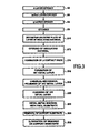
- FIG. 3 is a flow diagram of the principal steps implemented in the first embodiment described in FIGS. 2A to 2I ;
- FIGS. 4A to 4I are schematic perspective and cross-sectional views showing the manufacture of LED devices in accordance with a second embodiment of the disclosure.
- FIG. 5 is a flow diagram of the principal steps implemented in the second embodiment described in FIGS. 4A to 4I .
- the disclosure applies to the manufacture of elemental LED or photovoltaic (i.e., solar cell) structures, each comprising at least one p-type layer, an active zone and an n-type layer.
- FIGS. 2A to 2I and 3 A method of manufacturing LED devices in accordance with a first embodiment of the disclosure is now described in reference to FIGS. 2A to 2I and 3 .
- the method is implemented from a plate or support substrate 10 .
- the support substrate 10 is sapphire in this example, other materials, however, being possible, notably such as silicon, silicon carbide or germanium.
- n-type layer 12 (about 1 or 2 ⁇ m in thickness), an active layer 18 (about 10 nm) and a p-type layer 16 (between about 100 nm and 200 nm in thickness) are first deposited successively by epitaxy on the support substrate ( 10 ) (respectively, S 2 , S 4 and S 6 , FIG. 2A ).
- the manner in which these layers are prepared is known to the person skilled in the art and, thus, will not be described in further detail in this document.
- n- and p-type layers can be formed in the reverse order and can include several sub-layers of different compositions, thicknesses or dopant concentrations, comprising unintentionally doped sub-layers.
- the active layer 18 is a light-emitting (electroluminescent) layer that can be formed of a single thick or thin layer or of a plurality of layers of light-emitting quantum wells separated from each other by barrier layers.
- An etching step (S 8 , FIG. 2B ) is then carried out in order to dispose trenches 19 throughout the thickness of the p-type layer 16 (and, optionally, also in a portion of the thickness of the active layer 18 ) in order to form p-type islands 20 in layer 16 .
- a structure 28 comprising a plurality of elemental LED structures 25 each comprising a p-type insulated island 20 , an active layer 18 and an n-type layer 12 . It will be noted that the active layer 18 and the n-type layer 12 are here common to all of the elemental LED structures 25 .
- each p-type island 20 has here a square shape with sides 1 mm in length.
- the shape and dimensions of the p-type islands 20 which define the shape and at least part of the dimensions of the final LEDs, can obviously be different, with the islands 20 notably being able to have a circular shape.
- a layer of insulating material 30 is then deposited by plasma-enhanced chemical vapor deposition (PECVD) in order to cover the exposed surface of the elemental LED structures 25 and trenches 19 (step S 10 , FIG. 2C ).
- PECVD plasma-enhanced chemical vapor deposition
- this layer of insulating material 30 is planarized by chemical-mechanical polishing (CMP) or by any other suitable polishing technique (chemical etching, etc.) ( FIG. 2C ).
- CMP chemical-mechanical polishing
- the SiO 2 layer 30 can also be formed by the well-known spin-on glass (SOG) technique, which consists of depositing, on the substrate in rotation on a spinner, a viscous SiO 2 precursor composition. With this deposition technique, the SiO 2 layer has a satisfactory surface quality that does not require a post-deposition polishing step.
- SOG spin-on glass
- the insulating layer 30 is then opened, for example, by dry or wet selective chemical etching, on top of each p-type island 20 (step S 12 , FIG. 2D ).
- the openings 32 thus made are delimited by the residual portion 34 of the insulating layer 30 .
- an etching mask comprising a protective resin layer with openings (resin-free zones) delimiting the zones to be etched in the structure.
- the p contact pads 36 are then formed in the openings 32 by deposition in the latter of at least one conductive material (step S 14 , FIG. 2E ). During deposition of the contact pad 36 materials, the mask used is preserved for etching the openings 32 . Once the p contact pads 36 are formed, the protective resin of the etching mask is removed, which makes it possible to remove at the same time the constitutive materials of the p contact pads 36 deposited beyond the openings 32 .
- the method thus makes it possible to form electrical contact pads collectively on the whole of the elemental structures 25 present on the support substrate 10 .
- the collective formation provides a considerable improvement in device manufacturing yields.
- the layer forming the p contact pads 36 can notably include:
- one has a structure 38 in the form of a plate with a plurality of elemental structures 25 , each provided with a p contact pad 36 .
- the metal layer 40 is prepared, for example, by plasma-enhanced chemical vapor deposition (PECVD) or any other technique known to the person skilled in the art adapted to the formation of thin layers (SOG technique, etc.).
- PECVD plasma-enhanced chemical vapor deposition
- the metal deposition can, for example, be carried out completely by PVD (in the case of a metal layer 40 of aluminum, for example) or CVD, optionally followed by an electrodeposition phase.
- the deposition technique used depends on the metals constituting layer 40 .
- the metal layer 40 thus deposited follows to a certain extent the form of the underlying topography, in particular, the contours formed by the insulating portions 34 in relation to the p contact pads 36 .
- the insulating portions 34 form “steps” about 1 ⁇ m in height in relation to the adjacent p islands 20 .
- the thickness of the metal layer 40 is selected in order to then be able to be planarized adequately during step S 18 to follow (see below). In this example, the thickness of the metal layer is about 3 ⁇ m.
- the metal layer 40 can include a plurality of conductive sub-layers or can be composed of a single layer of conductive material.
- the metal layer 40 can include, for example, at least one sub-layer composed of one of the following conductive materials (or a combination of at least two): copper, aluminum, titanium and tungsten.
- the metal layer 40 is composed of a single layer formed, for example, of one of the materials mentioned above.
- the metal layer 40 is then prepared by chemical-mechanical polishing (CMP) so that an upper surface 42 a of the residual metal layer 42 has a sufficient planarity to enable subsequent bonding (step S 18 , FIG. 2G ).
- CMP chemical-mechanical polishing
- This polishing makes it possible, for example, to obtain a surface roughness 42 a less than or equal to 1 nm RMS, and preferably less than or equal to 0.5 nm RMS (it should be noted that the roughness values in RMS given in the disclosure correspond to a surface of 1 ⁇ m ⁇ 1 ⁇ m).
- the required roughness depends, in particular, on the bonding technique to be used during the bonding step S 22 to come (see below).
- polishing S 18 is followed by a step of cleaning of the upper surface 42 a of the metal layer 42 in order to eliminate the particles resulting from the polishing step S 18 (step S 20 , FIG. 2G ).
- Cleaning S 20 must be carried out in such a way as not to alter the roughness of the exposed surface 42 a obtained beforehand at the conclusion of the polishing step S 18 . Furthermore, this cleaning step S 20 must make it possible to remove a maximum of the residues that can result from the polishing S 18 of the exposed surface 42 a.
- a structure 45 is obtained in the form of a plate with a plurality of elemental LED structures 25 , each provided with a p contact pad, these structures 25 being covered with a planar metal layer 42 .
- the roughness required for the metal layer 42 can nevertheless vary somewhat according to the bonding technique to be employed in the bonding step S 22 to come (see below).
- CMP chemical-mechanical polishing
- step S 18 a second chemical-mechanical polishing is carried out as indicated in step S 18 in order to adequately planarize the exposed surface of the metal layer 40 .
- This variant makes it possible to substantially save the quantity of metal to be deposited to form the metal layer 40 (the contours underlying the metal layer 40 being removed during the first polishing step). Such savings are particularly advantageous when the metal used is expensive (the case for gold, for example).
- this variant involves an additional polishing step that also has an impact in terms of cost and productivity.
- a transfer substrate (or receiver substrate) 50 is bonded on the upper surface 42 a of structure 45 , in order to obtain a new structure 52 (step S 22 , FIG. 2H ).
- the transfer substrate 50 can be semiconductor material (silicon, for example) or metal (molybdenum, tungsten, etc.).
- the transfer substrate 50 comprises, on its bonding surface 50 a , a metal layer 46 that is brought into contact with metal layer 42 during the bonding step S 22 .
- Metal layer 42 can be composed of at least one among the following elements: Cu, Al, Ti and W.
- metal layers 42 and 46 can be of the same composition or of different compositions as the case may be.
- the transfer substrate 50 consists of a single metal plate (e.g., a plate of copper, tungsten, etc.). In this case, one surface of the body of the transfer substrate 50 is brought directly into contact with the metal layer 42 during the bonding step S 22 .
- the bonding surface 50 a of the transfer substrate 50 is planar in order to be able to carry out bonding with the structure 45 under favorable conditions.
- the roughness required for the bonding surface 50 a can nevertheless vary somewhat according to the bonding technique employed during the assembly step S 22 .
- assembly of the structure 45 on the transfer substrate 50 is carried out by bonding the metal layers 42 and 46 by molecular adhesion (at room temperature (between 20° C. and 30° C., for example).
- molecular adhesion at room temperature (between 20° C. and 30° C., for example).
- the roughness of the bonding surfaces 42 a and 50 a of the metal layers 42 and 46 is less than 1 nm RMS, and preferably less than or equal to 0.5 nm RMS.
- the step S 18 of polishing of metal layer 42 must thus be configured in such a way as to achieve such a roughness.
- a polishing step can be carried out on the bonding surface 50 a of the transfer substrate 50 before bonding with the structure 45 .
- the required roughness can, however, be achieved without such a polishing of the transfer substrate 50 being necessary: this can be the case, for example, when the metal layer 46 is a very thin layer (5 nm, for example) or the transfer substrate 50 is completely metallic.
- the principle of bonding by molecular adhesion is based on the bringing of two surfaces (here, surfaces 42 a and 50 a ) into direct contact, i.e., without the use of a specific bonding material (adhesive, wax, solder, etc.).
- a specific bonding material adheresive, wax, solder, etc.
- Such an operation requires that the surfaces to be bonded are sufficiently smooth and free of particles or contamination and that they are brought sufficiently close to make it possible to initiate contact, typically at a distance of less than a few nanometers.
- the attractive forces between the two surfaces are great enough to cause molecular adhesion (bonding induced by the sum of the attractive forces (van der Waals forces) of the electron interactions between the atoms or molecules of the two surfaces to be bonded).
- Bonding by molecular adhesion can be initiated by the application of a pressure point on at least one position of the structure 45 and/or the transfer substrate 50 (preferably on the periphery of the plate).
- the bonding wave between these two plates is then propagated from the point where pressure was applied.
- the application of such a pressure is not, however, obligatory to initiate the propagation of the bonding wave.
- annealing can be carried out at a moderate temperature (preferably less than or equal to 100° C.) in order to strengthen the bonding of the structure 45 on the transfer substrate 50 .
- the bonding in step S 22 is carried out by compression at room temperature.
- This technique makes it possible to obtain the bonding of structure 45 on transfer substrate 50 notably when the roughness of surfaces 42 a and/or 50 a are greater (typically between 0.5 and 5 nm RMS) and, in particular, when surfaces 42 a and 50 a are not sufficiently planar to allow bonding by molecular adhesion.
- the bonding in step S 22 is carried out by compression at a temperature less than or equal to 100° C.
- This moderate rise in temperature can be carried out in order to facilitate the bonding of structure 45 on transfer substrate 50 .
- the temperature applied during compression bonding is a function of the materials of substrates 10 and 50 and, more particularly, a function of the CTE of the two substrates 10 and 50 .
- the chosen temperature must indeed be such that the risks of fractures due to a CTE mismatch are minimal.
- the transfer substrate 50 must preferably make it possible to ensure good mechanical support for the final LED devices, as well as access to the p contact pads 36 .
- the transfer substrate 50 comprises from the side of its bonding surface 50 a copper contact pads (not shown) insulated from each other by portions of insulating material, these portions being SiN, for example. Each of these contact pads is formed at a location in alignment with at least part of a p contact pad 36 . Access to the contact pads of transfer substrate 50 located on surface 50 a is, for example, ensured by vertical electronic connections (not shown), also called “vias,” crossing the thickness of transfer substrate 50 to its opposite surface 50 b.
- the transfer substrate 50 can be composed notably of alumina or polycrystalline A1N, good thermal conductors, or of silicon.
- the support substrate 10 is removed, for example, by the well-known technique of laser lift-off, notably in the case of a sapphire substrate, or by chemical etching (step S 24 , FIG. 2I ).
- the support substrate 10 can be reused.
- surface 60 a of LEDs structure 60 can be etched in order to remove any residues remaining from support substrate 10 and can be structured to increase the extraction of light therefrom (step S 26 , FIG. 2I ).
- the etching can be carried out by reactive plasma etching (chlorinated or fluorinated) or by UV-assisted chemical (PEC) etching.
- n contact pads on n-type layer 12 .
- the formation of these n contact pads can be carried out collectively on the whole of the plate before the cutting step (in order to wire all the LED structures at the same time) or, alternatively, these pads can be prepared independently for each LED device once the cutting step is carried out.
- a layer of luminophoric material capable of converting the light emitted by the devices into white light can also be deposited on surface 60 a of LEDs structure 60 , for example, by applying a liquid phosphorus-based composition on surface 60 a followed by annealing to evaporate the dispersion solvent (spin-on glass).
- the LED devices can be provided with microstructures such as Fresnel lenses, for example, by nano- or micro-printing microstructures on the surface 60 a of the structure 60 .
- the inventive manufacturing method advantageously makes it possible to be freed from the mechanical stresses resulting from the pressure and temperature conditions required for bonding by traditional thermocompression (as indicated above).
- the choice of material to use to form the support substrate and the transfer substrate is thus considerably expanded since strict CTE compatibility with the elemental LED structure is no longer required. It thus becomes possible to choose, for example, any material to form the support substrate: it can, for example, be a substrate of silicon (widely available and relatively economical in large volumes) or of metal (molybdenum, etc.).
- FIGS. 4A to 4I and 5 represent the manufacture of LED devices in accordance with a second embodiment of the disclosure.
- This second embodiment is on the whole very similar to the first embodiment described above in reference to FIGS. 2A-2I and 3 .
- This second embodiment differs from the first in that the elemental LED structures (here noted 125 ) are formed on a composite growth substrate 100 , the latter comprising a support substrate 110 , a buried layer 102 and growth islands 104 ( FIGS. 2A and 2B ).
- the support substrate (here 110 ) consists of sapphire.
- Substrate 110 can also be composed of a semiconductor material, notably, such as silicon, silicon carbide or germanium.
- the buried layer 102 is an adaptation layer prepared here in SiO 2 .
- the growth islands 104 are obtained from a growth layer of relaxed material, here a layer of InGaN prepared, for example, by epitaxial growth on a seed layer of GaN and then transferred onto the support substrate 110 via the buried layer 102 .
- Trenches 119 were here prepared in the growth layer so as to delimit the InGaN growth islands 104 .
- the trenches 119 also make it possible to reduce the InGaN surface to be relaxed.
- the relaxation of the InGaN layer is carried out in advance of the inventive manufacturing method by means, for example, of an annealing of a slightly viscous layer (e.g., borophosphosilicate glass (BPSG)) disposed beforehand under the InGaN (not shown).
- a slightly viscous layer e.g., borophosphosilicate glass (BPSG)
- the elemental LED structures 125 are formed by successively depositing by epitaxy on the growth islands 104 an n-type layer 112 , an active layer 118 and a p-type layer 120 (steps S 102 , S 104 and S 106 , respectively) according to the same conditions as during the respective steps S 2 , S 4 and S 6 described above in the first embodiment.
- This second embodiment differs from the first described above in that the trenches 119 are disposed in order to completely separate the elemental structures 125 from each other (i.e., the n-type layer 112 and the active layer 118 of an elemental structure 125 are not common to the other elemental structures 125 ).
- next steps S 110 , S 112 , S 114 , S 116 , S 118 , S 120 , S 122 , S 124 and S 126 are carried out according to the same conditions as steps S 10 , S 12 , S 14 , S 16 , S 18 , S 20 , S 22 , S 24 and S 26 described above and, thus, they will not be described again for reasons of simplicity.
- Elements 130 , 132 , 134 , 136 , 138 , 140 , 142 , 145 , 146 , 150 , 152 and 160 notably correspond to elements 30 , 32 , 34 , 36 , 38 , 40 , 42 , 45 , 46 , 50 , 52 and 60 , respectively, described above and were prepared according to the same conditions.
- the second embodiment also differs from the first embodiment described above in that it comprises, after the removal S 124 of the support substrate 110 , the elimination S 125 of the buried layer 102 and then of the growth islands 104 , for example, by chemical etching ( FIG. 4I ).
- the buried layer 102 of SiO 2 makes it possible here to facilitate the disassembly of the support substrate 110 .
- step S 125 it is possible to remove any residues from the support substrate 110 , the buried layer 102 and the growth islands 104 in the same manner as in the elimination step S 25 of the first embodiment.
Abstract
Description
-
- a metal such as Ni, Pd or Pt with a thickness between 1 Å and 5 nm, in order to obtain a good resistivity and a good ohmic character,
- a reflector, for example, in the form of a layer of Ag with a thickness of about 100 nm, in order to return to the emitting surface the photons leaving toward the opposite surface (i.e., those moving toward the p-type layer when the structure is transferred to the final substrate, the emitting surface thus being found on the side of the n-type layer 12), and
- a diffusion barrier, for example, in the form of a layer of WN or TiN with a thickness between 20 and 50 nm.
Claims (14)
Applications Claiming Priority (7)
| Application Number | Priority Date | Filing Date | Title |
|---|---|---|---|
| FR1255934A FR2992466A1 (en) | 2012-06-22 | 2012-06-22 | Method for manufacturing e.g. LED device, involves forming insulating material portion on sides of p-type layer, active layer and portion of n-type layer, and exposing contact studs over another portion of n-type layer |
| FR1255931 | 2012-06-22 | ||
| FR1255934 | 2012-06-22 | ||
| FR1255931A FR2992465B1 (en) | 2012-06-22 | 2012-06-22 | METHOD FOR THE COLLECTIVE PRODUCTION OF LEDS AND STRUCTURE FOR THE COLLECTIVE MANUFACTURE OF LEDS |
| FR1257617A FR2992473B1 (en) | 2012-06-22 | 2012-08-06 | METHOD FOR MANUFACTURING LED STRUCTURES OR SOLAR CELLS |
| FR1257617 | 2012-08-06 | ||
| PCT/EP2013/062423 WO2013189857A1 (en) | 2012-06-22 | 2013-06-14 | Method of manufacturing structures of leds or solar cells |
Related Parent Applications (1)
| Application Number | Title | Priority Date | Filing Date |
|---|---|---|---|
| PCT/EP2013/062423 A-371-Of-International WO2013189857A1 (en) | 2012-06-22 | 2013-06-14 | Method of manufacturing structures of leds or solar cells |
Related Child Applications (1)
| Application Number | Title | Priority Date | Filing Date |
|---|---|---|---|
| US15/332,412 Continuation US9865786B2 (en) | 2012-06-22 | 2016-10-24 | Method of manufacturing structures of LEDs or solar cells |
Publications (2)
| Publication Number | Publication Date |
|---|---|
| US20150115290A1 US20150115290A1 (en) | 2015-04-30 |
| US9478707B2 true US9478707B2 (en) | 2016-10-25 |
Family
ID=50864365
Family Applications (2)
| Application Number | Title | Priority Date | Filing Date |
|---|---|---|---|
| US14/405,632 Active US9478707B2 (en) | 2012-06-22 | 2013-06-14 | Method of manufacturing structures of LEDs or solar cells |
| US15/332,412 Active US9865786B2 (en) | 2012-06-22 | 2016-10-24 | Method of manufacturing structures of LEDs or solar cells |
Family Applications After (1)
| Application Number | Title | Priority Date | Filing Date |
|---|---|---|---|
| US15/332,412 Active US9865786B2 (en) | 2012-06-22 | 2016-10-24 | Method of manufacturing structures of LEDs or solar cells |
Country Status (8)
| Country | Link |
|---|---|
| US (2) | US9478707B2 (en) |
| EP (1) | EP2865019B1 (en) |
| JP (1) | JP6269664B2 (en) |
| KR (1) | KR102087754B1 (en) |
| CN (1) | CN104396030B (en) |
| FR (2) | FR2992466A1 (en) |
| TW (1) | TWI493761B (en) |
| WO (1) | WO2013189857A1 (en) |
Cited By (6)
| Publication number | Priority date | Publication date | Assignee | Title |
|---|---|---|---|---|
| WO2018167426A2 (en) | 2017-03-17 | 2018-09-20 | Soitec | Growth substrate for forming optoelectronic devices, method for producing such a substrate and use of the substrate, in particular in the field of micro-displays |
| US10084011B1 (en) | 2017-03-17 | 2018-09-25 | Soitec | Growth substrate for forming optoelectronic devices, method for manufacturing such a substrate, and use of the susbstrate, in particular in the field of micro-display screens |
| US20200171544A1 (en) * | 2018-11-29 | 2020-06-04 | Ascent Ventures, Llc | High Frequency Ultrasonic Transducer and Method of Fabrication |
| US11081521B2 (en) | 2018-03-13 | 2021-08-03 | Soitec | Process for manufacturing a plurality of crystalline semiconductor islands having a variety of lattice parameters |
| US11171256B2 (en) | 2018-03-13 | 2021-11-09 | Soitec | Process for manufacturing a plurality of crystalline semiconductor islands having a variety of lattice parameters |
| US11322655B2 (en) * | 2017-08-01 | 2022-05-03 | Osram Oled Gmbh | Method for producing an optoelectronic component, and optoelectronic component |
Families Citing this family (25)
| Publication number | Priority date | Publication date | Assignee | Title |
|---|---|---|---|---|
| FR2992466A1 (en) | 2012-06-22 | 2013-12-27 | Soitec Silicon On Insulator | Method for manufacturing e.g. LED device, involves forming insulating material portion on sides of p-type layer, active layer and portion of n-type layer, and exposing contact studs over another portion of n-type layer |
| DE102013103601A1 (en) * | 2013-04-10 | 2014-10-16 | Osram Opto Semiconductors Gmbh | Optoelectronic component and method for producing an optoelectronic component |
| FR3023065B1 (en) * | 2014-06-27 | 2017-12-15 | Commissariat Energie Atomique | P-N JUNCTION OPTOELECTRONIC DEVICE FOR IONIZATION OF FIELD EFFECT DOPANTS |
| DE102015108056A1 (en) * | 2015-05-21 | 2016-11-24 | Osram Opto Semiconductors Gmbh | Optoelectronic semiconductor component, optoelectronic assembly and method for producing an optoelectronic semiconductor component |
| FR3038127B1 (en) | 2015-06-24 | 2017-06-23 | Commissariat Energie Atomique | METHOD FOR MANUFACTURING A PLURALITY OF ISLET-SHAPED DIPOLES HAVING SELF-ALIGNED ELECTRODES |
| FR3043254B1 (en) * | 2015-11-04 | 2018-03-16 | Commissariat A L'energie Atomique Et Aux Energies Alternatives | METHOD FOR PRODUCING AN ELECTRONIC DEVICE |
| EP3913680A1 (en) * | 2016-05-13 | 2021-11-24 | Commissariat à l'Energie Atomique et aux Energies Alternatives | Method for manufacturing an optoelectronic device comprising a plurality of gallium nitride diodes |
| WO2017200845A1 (en) | 2016-05-20 | 2017-11-23 | Lumileds Llc | Method of forming a p-type layer for a light emitting device |
| KR102419593B1 (en) * | 2017-10-23 | 2022-07-12 | 삼성전자주식회사 | Light emitting diode apparatus and manufacturing method thereof |
| US10804429B2 (en) * | 2017-12-22 | 2020-10-13 | Lumileds Llc | III-nitride multi-wavelength LED for visible light communication |
| FR3076170B1 (en) * | 2017-12-22 | 2020-05-15 | Commissariat A L'energie Atomique Et Aux Energies Alternatives | METHOD FOR DEFERRING ELECTROLUMINESCENT STRUCTURES |
| US11515299B2 (en) | 2018-05-16 | 2022-11-29 | Industrial Technology Research Institute | Method for manufacturing display array |
| TWI688121B (en) | 2018-08-24 | 2020-03-11 | 隆達電子股份有限公司 | Light emitting diode structure |
| US11342479B2 (en) | 2018-09-11 | 2022-05-24 | Facebook Technologies, Llc | Reducing bowing of materials before wafer-to-wafer bonding for LED manufacturing |
| US11056611B2 (en) * | 2018-09-11 | 2021-07-06 | Facebook Technologies, Llc | Mesa formation for wafer-to-wafer bonding |
| US11145786B2 (en) | 2018-09-11 | 2021-10-12 | Facebook Technologies, Llc | Methods for wafer-to-wafer bonding |
| WO2020073306A1 (en) * | 2018-10-12 | 2020-04-16 | Boe Technology Group Co., Ltd. | Micro light emitting diode apparatus and fabricating method thereof |
| US11152540B2 (en) | 2019-07-29 | 2021-10-19 | Lextar Electronics Corporation | Light emitting diode structure and method of manufacturing thereof |
| GB2586862B (en) * | 2019-09-06 | 2021-12-15 | Plessey Semiconductors Ltd | LED precursor incorporating strain relaxing structure |
| US11038088B2 (en) | 2019-10-14 | 2021-06-15 | Lextar Electronics Corporation | Light emitting diode package |
| CN114730813A (en) * | 2019-12-13 | 2022-07-08 | 苏州晶湛半导体有限公司 | Method for manufacturing semiconductor structure |
| US11211527B2 (en) | 2019-12-19 | 2021-12-28 | Lumileds Llc | Light emitting diode (LED) devices with high density textures |
| US11264530B2 (en) | 2019-12-19 | 2022-03-01 | Lumileds Llc | Light emitting diode (LED) devices with nucleation layer |
| JP7424038B2 (en) * | 2019-12-23 | 2024-01-30 | セイコーエプソン株式会社 | Light emitting device and projector |
| TWI740438B (en) * | 2020-03-31 | 2021-09-21 | 聚積科技股份有限公司 | Transfer method of miniature light-emitting diode |
Citations (20)
| Publication number | Priority date | Publication date | Assignee | Title |
|---|---|---|---|---|
| US3921885A (en) * | 1973-06-28 | 1975-11-25 | Rca Corp | Method of bonding two bodies together |
| US6037644A (en) * | 1997-09-12 | 2000-03-14 | The Whitaker Corporation | Semi-transparent monitor detector for surface emitting light emitting devices |
| US6281524B1 (en) | 1997-02-21 | 2001-08-28 | Kabushiki Kaisha Toshiba | Semiconductor light-emitting device |
| US6921741B2 (en) * | 2000-12-06 | 2005-07-26 | The Regents Of The University Of California | Substrate structure for growth of highly oriented and/or epitaxial layers thereon |
| US20050280007A1 (en) | 2004-06-17 | 2005-12-22 | Tzu-Hsuan Hsu | Image sensor with optical guard ring and fabrication method thereof |
| US20060043384A1 (en) | 2004-08-24 | 2006-03-02 | Samsung Electro-Mechanics Co., Ltd. | Vertical nitride semiconductor light emitting diode |
| US20060169994A1 (en) | 2005-02-03 | 2006-08-03 | United Epitaxy Company, Ltd. | Light emitting device and manufacture method thereof |
| US20080179602A1 (en) | 2007-01-22 | 2008-07-31 | Led Lighting Fixtures, Inc. | Fault tolerant light emitters, systems incorporating fault tolerant light emitters and methods of fabricating fault tolerant light emitters |
| US20090032970A1 (en) * | 2007-07-31 | 2009-02-05 | Park Chang-Min | Stacking of integrated circuits using glassy metal bonding |
| US20100006881A1 (en) | 2008-07-08 | 2010-01-14 | Seoul Opto Device Co., Ltd. | Light emitting device and method for fabricating the same |
| US20100022039A1 (en) * | 2008-07-28 | 2010-01-28 | Foxconn Technology Co., Ltd. | Method of making light emitting diodes |
| US20100019222A1 (en) | 2008-07-25 | 2010-01-28 | High Power Opto.Inc. | Low-temperature led chip metal bonding layer |
| US20100308455A1 (en) | 2008-12-09 | 2010-12-09 | Young Hae KIM | Method for Manufacturing Hetero-Bonded Wafer |
| KR20110058122A (en) | 2009-11-25 | 2011-06-01 | 고려대학교 산학협력단 | Vertical structured semiconductor light emitting device and method for producing thereof |
| US20110174376A1 (en) | 2010-01-19 | 2011-07-21 | Amberwave, Inc. | Monocrystalline Thin Cell |
| EP2390933A1 (en) | 2010-05-24 | 2011-11-30 | Kabushiki Kaisha Toshiba | Semiconductor light emitting device |
| US20120074441A1 (en) | 2010-09-24 | 2012-03-29 | Seoul Semiconductor Co., Ltd. | Wafer-level light emitting diode package and method of fabricating the same |
| US20120126259A1 (en) * | 2010-11-24 | 2012-05-24 | Hitachi Cable, Ltd. | Light emitting diode |
| WO2012066033A1 (en) | 2010-11-18 | 2012-05-24 | Soitec | Method for forming a buried metal layer structure |
| US20150171273A1 (en) * | 2010-11-04 | 2015-06-18 | Koninklijke Philips Electronics N.V. | Solid state light emitting devices based on crystallographically relaxed structures |
Family Cites Families (58)
| Publication number | Priority date | Publication date | Assignee | Title |
|---|---|---|---|---|
| US5565266A (en) | 1993-06-14 | 1996-10-15 | Eastman Kodak Company | Multilayer magnetooptic recording media |
| US5563000A (en) | 1994-03-11 | 1996-10-08 | Eastman Kodak Company | Multilayer magnetooptic recording media |
| JP2000020937A (en) | 1998-07-03 | 2000-01-21 | Hitachi Ltd | Magnetic recording medium and magnetic storage device using the same |
| JP4189146B2 (en) | 2001-07-19 | 2008-12-03 | アルプス電気株式会社 | Exchange coupling film and magnetic sensing element using the exchange coupling film |
| JP2003031870A (en) | 2001-07-19 | 2003-01-31 | Alps Electric Co Ltd | Exchange coupling film and magnetic sensor element using the same |
| JP4198900B2 (en) | 2001-07-19 | 2008-12-17 | アルプス電気株式会社 | Exchange coupling film and magnetic sensing element using the exchange coupling film |
| US20030189215A1 (en) | 2002-04-09 | 2003-10-09 | Jong-Lam Lee | Method of fabricating vertical structure leds |
| JP2003332649A (en) | 2002-05-14 | 2003-11-21 | Alps Electric Co Ltd | Magnetic detecting element |
| US6653704B1 (en) | 2002-09-24 | 2003-11-25 | International Business Machines Corporation | Magnetic memory with tunnel junction memory cells and phase transition material for controlling current to the cells |
| US7092220B2 (en) | 2003-07-29 | 2006-08-15 | Hitachi Global Storage Technologies | Apparatus for enhancing thermal stability, improving biasing and reducing damage from electrostatic discharge in self-pinned abutted junction heads having a first self-pinned layer extending under the hard bias layers |
| US7282277B2 (en) | 2004-04-20 | 2007-10-16 | Seagate Technology Llc | Magnetic recording media with Cu-containing magnetic layers |
| US7449345B2 (en) | 2004-06-15 | 2008-11-11 | Headway Technologies, Inc. | Capping structure for enhancing dR/R of the MTJ device |
| JP2006165059A (en) | 2004-12-02 | 2006-06-22 | Sony Corp | Storage element and memory |
| JP2006269664A (en) * | 2005-03-23 | 2006-10-05 | Fuji Xerox Co Ltd | Light emitting device, optical communication system, and method for manufacturing light emitting device |
| JP4767035B2 (en) * | 2005-04-12 | 2011-09-07 | シャープ株式会社 | Nitride-based semiconductor light-emitting device and manufacturing method thereof |
| JP2006334652A (en) * | 2005-06-03 | 2006-12-14 | Ebara Corp | Metal joining method |
| JP4933130B2 (en) | 2006-02-16 | 2012-05-16 | 昭和電工株式会社 | GaN-based semiconductor light-emitting device and manufacturing method thereof |
| JP2007271676A (en) * | 2006-03-30 | 2007-10-18 | Kyocera Corp | Fiber type optical path, fiber type component and optical module |
| JP2008124381A (en) | 2006-11-15 | 2008-05-29 | Sharp Corp | Solar battery |
| US20080170329A1 (en) | 2007-01-11 | 2008-07-17 | Seagate Technology Llc | Granular perpendicular magnetic recording media with improved corrosion resistance by SUL post-deposition heating |
| US20100035085A1 (en) | 2007-02-03 | 2010-02-11 | Wd Media, Inc. | Perpendicular magnetic recording medium with improved magnetic anisotropy field |
| JP2008263126A (en) * | 2007-04-13 | 2008-10-30 | Oki Data Corp | Semiconductor apparatus, method of manufacturing the same, led head, and image formation apparatus |
| JP2009105123A (en) * | 2007-10-22 | 2009-05-14 | Showa Denko Kk | Light-emitting diode, and manufacturing method thereof |
| JP2009116930A (en) | 2007-11-02 | 2009-05-28 | Hitachi Global Storage Technologies Netherlands Bv | Vertical magnetic recording medium and magnetic recording and reproducing device using the same |
| KR20090074396A (en) | 2008-01-02 | 2009-07-07 | 삼성전자주식회사 | Information storage media using ferroelectric material, manufacturing method of the information storage media, and information storage device adopting the same |
| WO2009113659A1 (en) * | 2008-03-13 | 2009-09-17 | 昭和電工株式会社 | Semiconductor light-emitting device and method for manufacturing the same |
| KR20090122728A (en) * | 2008-05-26 | 2009-12-01 | 삼성전자주식회사 | Non-linear solar cell module |
| US9117944B2 (en) * | 2008-09-24 | 2015-08-25 | Koninklijke Philips N.V. | Semiconductor light emitting devices grown on composite substrates |
| FR2936903B1 (en) | 2008-10-07 | 2011-01-14 | Soitec Silicon On Insulator | RELAXING A LAYER OF CONTAMINATED MATERIAL WITH APPLICATION OF A STIFFENER |
| EP2412006A1 (en) | 2009-02-05 | 2012-02-01 | S.O.I.Tec Silicon on Insulator Technologies | Epitaxial methods and structures for forming semiconductor materials |
| CN102449775B (en) * | 2009-06-05 | 2014-07-02 | 独立行政法人产业技术综合研究所 | Semiconductor wafer, photoelectric conversion device, method of producing semiconductor wafer, and method of producing photoelectric conversion device |
| US8580593B2 (en) | 2009-09-10 | 2013-11-12 | Micron Technology, Inc. | Epitaxial formation structures and associated methods of manufacturing solid state lighting devices |
| JP5493624B2 (en) | 2009-09-15 | 2014-05-14 | ソニー株式会社 | Image display device and electronic device |
| US9082534B2 (en) | 2009-09-15 | 2015-07-14 | Samsung Electronics Co., Ltd. | Magnetic element having perpendicular anisotropy with enhanced efficiency |
| JP5534763B2 (en) * | 2009-09-25 | 2014-07-02 | 株式会社東芝 | Semiconductor light emitting device manufacturing method and semiconductor light emitting device |
| JP2011148979A (en) | 2009-12-22 | 2011-08-04 | Panasonic Electric Works Co Ltd | Epoxy resin composition for printed wiring board, resin film, prepreg, resin sheet with metal foil, and flexible printed wiring board |
| JP2011171273A (en) | 2010-01-25 | 2011-09-01 | Hitachi Chem Co Ltd | Electrode paste composition and solar cell |
| JP2011198962A (en) | 2010-03-18 | 2011-10-06 | Toshiba Corp | Method for manufacturing semiconductor light emitting element |
| SG175482A1 (en) | 2010-05-04 | 2011-11-28 | Agency Science Tech & Res | Multi-bit cell magnetic memory with perpendicular magnetization and spin torque switching |
| US8786036B2 (en) | 2011-01-19 | 2014-07-22 | Headway Technologies, Inc. | Magnetic tunnel junction for MRAM applications |
| US8508006B2 (en) | 2011-05-10 | 2013-08-13 | Magic Technologies, Inc. | Co/Ni multilayers with improved out-of-plane anisotropy for magnetic device applications |
| US9245563B2 (en) | 2011-05-17 | 2016-01-26 | Showa Denko K.K. | Magnetic medium with an orientation control layer |
| JP5768498B2 (en) | 2011-05-23 | 2015-08-26 | ソニー株式会社 | Memory element and memory device |
| JP5177256B2 (en) | 2011-06-03 | 2013-04-03 | 富士電機株式会社 | Perpendicular magnetic recording medium and manufacturing method thereof |
| TWI434405B (en) * | 2011-06-07 | 2014-04-11 | Univ Nat Chiao Tung | Heterogeneous integration structure having integration circuit (ic) and light-emitting-diode (led) and method for fabricating the same |
| US8492169B2 (en) | 2011-08-15 | 2013-07-23 | Magic Technologies, Inc. | Magnetic tunnel junction for MRAM applications |
| US9679664B2 (en) | 2012-02-11 | 2017-06-13 | Samsung Electronics Co., Ltd. | Method and system for providing a smart memory architecture |
| US8871365B2 (en) | 2012-02-28 | 2014-10-28 | Headway Technologies, Inc. | High thermal stability reference structure with out-of-plane aniotropy to magnetic device applications |
| US8941950B2 (en) | 2012-05-23 | 2015-01-27 | WD Media, LLC | Underlayers for heat assisted magnetic recording (HAMR) media |
| FR2992466A1 (en) | 2012-06-22 | 2013-12-27 | Soitec Silicon On Insulator | Method for manufacturing e.g. LED device, involves forming insulating material portion on sides of p-type layer, active layer and portion of n-type layer, and exposing contact studs over another portion of n-type layer |
| KR101446338B1 (en) | 2012-07-17 | 2014-10-01 | 삼성전자주식회사 | Magnetic device and method of manufacturing the same |
| JP5961490B2 (en) | 2012-08-29 | 2016-08-02 | 昭和電工株式会社 | Magnetic recording medium and magnetic recording / reproducing apparatus |
| US20140242419A1 (en) | 2013-02-28 | 2014-08-28 | Showa Denko Hd Singapore Pte Ltd. | Perpendicular recording medium for hard disk drives |
| US9499899B2 (en) | 2013-03-13 | 2016-11-22 | Intermolecular, Inc. | Systems, methods, and apparatus for production coatings of low-emissivity glass including a ternary alloy |
| US9206078B2 (en) | 2013-03-13 | 2015-12-08 | Intermolecular, Inc. | Barrier layers for silver reflective coatings and HPC workflows for rapid screening of materials for such barrier layers |
| JP6199618B2 (en) | 2013-04-12 | 2017-09-20 | 昭和電工株式会社 | Magnetic recording medium, magnetic storage device |
| US9341685B2 (en) | 2013-05-13 | 2016-05-17 | HGST Netherlands B.V. | Antiferromagnetic (AFM) grain growth controlled random telegraph noise (RTN) suppressed magnetic head |
| JPWO2014184988A1 (en) | 2013-05-16 | 2017-02-23 | パナソニックIpマネジメント株式会社 | Semiconductor device and manufacturing method thereof |
-
2012
- 2012-06-22 FR FR1255934A patent/FR2992466A1/en active Pending
- 2012-08-06 FR FR1257617A patent/FR2992473B1/en active Active
-
2013
- 2013-06-14 US US14/405,632 patent/US9478707B2/en active Active
- 2013-06-14 CN CN201380032574.0A patent/CN104396030B/en active Active
- 2013-06-14 KR KR1020147036038A patent/KR102087754B1/en active IP Right Grant
- 2013-06-14 EP EP13728426.1A patent/EP2865019B1/en active Active
- 2013-06-14 WO PCT/EP2013/062423 patent/WO2013189857A1/en active Application Filing
- 2013-06-14 JP JP2015517701A patent/JP6269664B2/en active Active
- 2013-06-21 TW TW102122243A patent/TWI493761B/en active
-
2016
- 2016-10-24 US US15/332,412 patent/US9865786B2/en active Active
Patent Citations (22)
| Publication number | Priority date | Publication date | Assignee | Title |
|---|---|---|---|---|
| US3921885A (en) * | 1973-06-28 | 1975-11-25 | Rca Corp | Method of bonding two bodies together |
| US6281524B1 (en) | 1997-02-21 | 2001-08-28 | Kabushiki Kaisha Toshiba | Semiconductor light-emitting device |
| US6037644A (en) * | 1997-09-12 | 2000-03-14 | The Whitaker Corporation | Semi-transparent monitor detector for surface emitting light emitting devices |
| US6921741B2 (en) * | 2000-12-06 | 2005-07-26 | The Regents Of The University Of California | Substrate structure for growth of highly oriented and/or epitaxial layers thereon |
| US20050280007A1 (en) | 2004-06-17 | 2005-12-22 | Tzu-Hsuan Hsu | Image sensor with optical guard ring and fabrication method thereof |
| US20060043384A1 (en) | 2004-08-24 | 2006-03-02 | Samsung Electro-Mechanics Co., Ltd. | Vertical nitride semiconductor light emitting diode |
| US20060169994A1 (en) | 2005-02-03 | 2006-08-03 | United Epitaxy Company, Ltd. | Light emitting device and manufacture method thereof |
| US20080179602A1 (en) | 2007-01-22 | 2008-07-31 | Led Lighting Fixtures, Inc. | Fault tolerant light emitters, systems incorporating fault tolerant light emitters and methods of fabricating fault tolerant light emitters |
| US20090032970A1 (en) * | 2007-07-31 | 2009-02-05 | Park Chang-Min | Stacking of integrated circuits using glassy metal bonding |
| US20100006881A1 (en) | 2008-07-08 | 2010-01-14 | Seoul Opto Device Co., Ltd. | Light emitting device and method for fabricating the same |
| US20100019222A1 (en) | 2008-07-25 | 2010-01-28 | High Power Opto.Inc. | Low-temperature led chip metal bonding layer |
| US20100022039A1 (en) * | 2008-07-28 | 2010-01-28 | Foxconn Technology Co., Ltd. | Method of making light emitting diodes |
| US20100308455A1 (en) | 2008-12-09 | 2010-12-09 | Young Hae KIM | Method for Manufacturing Hetero-Bonded Wafer |
| KR20110058122A (en) | 2009-11-25 | 2011-06-01 | 고려대학교 산학협력단 | Vertical structured semiconductor light emitting device and method for producing thereof |
| TW201138168A (en) | 2009-11-25 | 2011-11-01 | Korea University Ind & Amp Academic Collaboration Foundation | Vertical structured semiconductor light emitting device and its manufacturing method |
| US20120220063A1 (en) | 2009-11-25 | 2012-08-30 | Tae Yeon Seong | Vertical-structure semiconductor light emitting element and a production method therefor |
| US20110174376A1 (en) | 2010-01-19 | 2011-07-21 | Amberwave, Inc. | Monocrystalline Thin Cell |
| EP2390933A1 (en) | 2010-05-24 | 2011-11-30 | Kabushiki Kaisha Toshiba | Semiconductor light emitting device |
| US20120074441A1 (en) | 2010-09-24 | 2012-03-29 | Seoul Semiconductor Co., Ltd. | Wafer-level light emitting diode package and method of fabricating the same |
| US20150171273A1 (en) * | 2010-11-04 | 2015-06-18 | Koninklijke Philips Electronics N.V. | Solid state light emitting devices based on crystallographically relaxed structures |
| WO2012066033A1 (en) | 2010-11-18 | 2012-05-24 | Soitec | Method for forming a buried metal layer structure |
| US20120126259A1 (en) * | 2010-11-24 | 2012-05-24 | Hitachi Cable, Ltd. | Light emitting diode |
Non-Patent Citations (5)
| Title |
|---|
| European Communication pursuant to Article 94(3) EPC for European Application No. EP 13 729 948.3 dated Feb. 2, 2016, 7 pages. |
| International Preliminary Report on Patentability for International Application No. PCT/EP2013/062423 dated Dec. 23, 2014, 5 pages. |
| International Search Report for International Application No. PCT/EP2013/062423 dated Sep. 26, 2013, 4 pages. |
| International Written Opinion for International Application No. PCT/EP2013/062423 dated Sep. 26, 2013, 4 pages. |
| Taiwan Search Report for Taiwan Application No. 102122243 dated Dec. 25, 2014, 1 page. |
Cited By (7)
| Publication number | Priority date | Publication date | Assignee | Title |
|---|---|---|---|---|
| WO2018167426A2 (en) | 2017-03-17 | 2018-09-20 | Soitec | Growth substrate for forming optoelectronic devices, method for producing such a substrate and use of the substrate, in particular in the field of micro-displays |
| US10084011B1 (en) | 2017-03-17 | 2018-09-25 | Soitec | Growth substrate for forming optoelectronic devices, method for manufacturing such a substrate, and use of the susbstrate, in particular in the field of micro-display screens |
| EP4033531A1 (en) | 2017-03-17 | 2022-07-27 | Soitec | Method for manufacturing a plurality of crystalline semiconductor islands |
| US11322655B2 (en) * | 2017-08-01 | 2022-05-03 | Osram Oled Gmbh | Method for producing an optoelectronic component, and optoelectronic component |
| US11081521B2 (en) | 2018-03-13 | 2021-08-03 | Soitec | Process for manufacturing a plurality of crystalline semiconductor islands having a variety of lattice parameters |
| US11171256B2 (en) | 2018-03-13 | 2021-11-09 | Soitec | Process for manufacturing a plurality of crystalline semiconductor islands having a variety of lattice parameters |
| US20200171544A1 (en) * | 2018-11-29 | 2020-06-04 | Ascent Ventures, Llc | High Frequency Ultrasonic Transducer and Method of Fabrication |
Also Published As
| Publication number | Publication date |
|---|---|
| TWI493761B (en) | 2015-07-21 |
| US20170040518A1 (en) | 2017-02-09 |
| WO2013189857A1 (en) | 2013-12-27 |
| TW201405895A (en) | 2014-02-01 |
| KR102087754B1 (en) | 2020-03-11 |
| CN104396030A (en) | 2015-03-04 |
| CN104396030B (en) | 2017-07-14 |
| FR2992466A1 (en) | 2013-12-27 |
| JP6269664B2 (en) | 2018-01-31 |
| US9865786B2 (en) | 2018-01-09 |
| FR2992473B1 (en) | 2015-06-05 |
| KR20150023452A (en) | 2015-03-05 |
| US20150115290A1 (en) | 2015-04-30 |
| EP2865019B1 (en) | 2018-08-01 |
| FR2992473A1 (en) | 2013-12-27 |
| JP2015526889A (en) | 2015-09-10 |
| EP2865019A1 (en) | 2015-04-29 |
Similar Documents
| Publication | Publication Date | Title |
|---|---|---|
| US9865786B2 (en) | Method of manufacturing structures of LEDs or solar cells | |
| US11329034B2 (en) | Direct-bonded LED structure contacts and substrate contacts | |
| JP6177766B2 (en) | Semiconductor wafer bonding incorporating electrical and optical interconnects | |
| EP2865021B1 (en) | Method of collective manufacture of leds and structure for collective manufacture of leds. | |
| JP2019114804A (en) | Light-emitting device bonded to supporting substrate | |
| EP2438625B1 (en) | Method of forming a dielectric layer on a semiconductor light emitting device, and semiconductor light emitting device with a dielectric layer | |
| US9825198B2 (en) | Method of producing a plurality of optoelectronic semiconductor chips, and optoelectronic semiconductor chip | |
| KR20110058122A (en) | Vertical structured semiconductor light emitting device and method for producing thereof | |
| JP2007533133A (en) | Fabrication of reflective layer on semiconductor light emitting diode | |
| TWI536600B (en) | Semiconductor light emitting device and method of manufacturing the same | |
| US20180366618A1 (en) | Optoelectronic Semiconductor Devices with Enhanced Light Output | |
| US9853186B2 (en) | Producing a light-emitting semiconductor component by connecting first and second semiconductor bodies | |
| US11557691B2 (en) | Method of manufacturing a semiconductor device and semiconductor device | |
| KR102328383B1 (en) | Method for manufacturing optoelectronic semiconductor chip, and optoelectronic semiconductor chip | |
| TW201318236A (en) | GaN LEDs with improved area and method for making the same | |
| TW201316504A (en) | Electrically insulating bond for mounting a light emitting device | |
| TW201205865A (en) | Vertical light emitting diode device structure and method of fabricating the same |
Legal Events
| Date | Code | Title | Description |
|---|---|---|---|
| AS | Assignment |
Owner name: SOITEC, FRANCE Free format text: ASSIGNMENT OF ASSIGNORS INTEREST;ASSIGNOR:GUENARD, PASCAL;REEL/FRAME:035143/0268 Effective date: 20150310 |
|
| STCF | Information on status: patent grant |
Free format text: PATENTED CASE |
|
| MAFP | Maintenance fee payment |
Free format text: PAYMENT OF MAINTENANCE FEE, 4TH YEAR, LARGE ENTITY (ORIGINAL EVENT CODE: M1551); ENTITY STATUS OF PATENT OWNER: LARGE ENTITY Year of fee payment: 4 |
|
| MAFP | Maintenance fee payment |
Free format text: PAYMENT OF MAINTENANCE FEE, 8TH YEAR, LARGE ENTITY (ORIGINAL EVENT CODE: M1552); ENTITY STATUS OF PATENT OWNER: LARGE ENTITY Year of fee payment: 8 |