US9472873B1 - Reversible receptacle connector - Google Patents
Reversible receptacle connector Download PDFInfo
- Publication number
- US9472873B1 US9472873B1 US14/824,717 US201514824717A US9472873B1 US 9472873 B1 US9472873 B1 US 9472873B1 US 201514824717 A US201514824717 A US 201514824717A US 9472873 B1 US9472873 B1 US 9472873B1
- Authority
- US
- United States
- Prior art keywords
- contact
- insulating member
- receptacle
- conductive bridge
- plug
- Prior art date
- Legal status (The legal status is an assumption and is not a legal conclusion. Google has not performed a legal analysis and makes no representation as to the accuracy of the status listed.)
- Active
Links
- 230000002441 reversible effect Effects 0.000 title description 17
- YFSLABAYQDPWPF-UHFFFAOYSA-N 1,2,3-trichloro-4-(2,3,5-trichlorophenyl)benzene Chemical compound ClC1=CC(Cl)=C(Cl)C(C=2C(=C(Cl)C(Cl)=CC=2)Cl)=C1 YFSLABAYQDPWPF-UHFFFAOYSA-N 0.000 description 12
- 230000000694 effects Effects 0.000 description 3
- 239000002131 composite material Substances 0.000 description 2
- 239000002184 metal Substances 0.000 description 2
- 238000010276 construction Methods 0.000 description 1
- 238000000034 method Methods 0.000 description 1
Images


Classifications
-
- H—ELECTRICITY
- H01—ELECTRIC ELEMENTS
- H01R—ELECTRICALLY-CONDUCTIVE CONNECTIONS; STRUCTURAL ASSOCIATIONS OF A PLURALITY OF MUTUALLY-INSULATED ELECTRICAL CONNECTING ELEMENTS; COUPLING DEVICES; CURRENT COLLECTORS
- H01R12/00—Structural associations of a plurality of mutually-insulated electrical connecting elements, specially adapted for printed circuits, e.g. printed circuit boards [PCB], flat or ribbon cables, or like generally planar structures, e.g. terminal strips, terminal blocks; Coupling devices specially adapted for printed circuits, flat or ribbon cables, or like generally planar structures; Terminals specially adapted for contact with, or insertion into, printed circuits, flat or ribbon cables, or like generally planar structures
- H01R12/70—Coupling devices
- H01R12/71—Coupling devices for rigid printing circuits or like structures
- H01R12/72—Coupling devices for rigid printing circuits or like structures coupling with the edge of the rigid printed circuits or like structures
- H01R12/722—Coupling devices for rigid printing circuits or like structures coupling with the edge of the rigid printed circuits or like structures coupling devices mounted on the edge of the printed circuits
- H01R12/724—Coupling devices for rigid printing circuits or like structures coupling with the edge of the rigid printed circuits or like structures coupling devices mounted on the edge of the printed circuits containing contact members forming a right angle
-
- H—ELECTRICITY
- H01—ELECTRIC ELEMENTS
- H01R—ELECTRICALLY-CONDUCTIVE CONNECTIONS; STRUCTURAL ASSOCIATIONS OF A PLURALITY OF MUTUALLY-INSULATED ELECTRICAL CONNECTING ELEMENTS; COUPLING DEVICES; CURRENT COLLECTORS
- H01R12/00—Structural associations of a plurality of mutually-insulated electrical connecting elements, specially adapted for printed circuits, e.g. printed circuit boards [PCB], flat or ribbon cables, or like generally planar structures, e.g. terminal strips, terminal blocks; Coupling devices specially adapted for printed circuits, flat or ribbon cables, or like generally planar structures; Terminals specially adapted for contact with, or insertion into, printed circuits, flat or ribbon cables, or like generally planar structures
- H01R12/70—Coupling devices
- H01R12/7076—Coupling devices for connection between PCB and component, e.g. display
-
- H—ELECTRICITY
- H01—ELECTRIC ELEMENTS
- H01R—ELECTRICALLY-CONDUCTIVE CONNECTIONS; STRUCTURAL ASSOCIATIONS OF A PLURALITY OF MUTUALLY-INSULATED ELECTRICAL CONNECTING ELEMENTS; COUPLING DEVICES; CURRENT COLLECTORS
- H01R13/00—Details of coupling devices of the kinds covered by groups H01R12/70 or H01R24/00 - H01R33/00
- H01R13/64—Means for preventing incorrect coupling
- H01R13/642—Means for preventing incorrect coupling by position or shape of contact members
-
- H—ELECTRICITY
- H01—ELECTRIC ELEMENTS
- H01R—ELECTRICALLY-CONDUCTIVE CONNECTIONS; STRUCTURAL ASSOCIATIONS OF A PLURALITY OF MUTUALLY-INSULATED ELECTRICAL CONNECTING ELEMENTS; COUPLING DEVICES; CURRENT COLLECTORS
- H01R24/00—Two-part coupling devices, or either of their cooperating parts, characterised by their overall structure
- H01R24/58—Contacts spaced along longitudinal axis of engagement
-
- H—ELECTRICITY
- H01—ELECTRIC ELEMENTS
- H01R—ELECTRICALLY-CONDUCTIVE CONNECTIONS; STRUCTURAL ASSOCIATIONS OF A PLURALITY OF MUTUALLY-INSULATED ELECTRICAL CONNECTING ELEMENTS; COUPLING DEVICES; CURRENT COLLECTORS
- H01R24/00—Two-part coupling devices, or either of their cooperating parts, characterised by their overall structure
- H01R24/60—Contacts spaced along planar side wall transverse to longitudinal axis of engagement
-
- H—ELECTRICITY
- H01—ELECTRIC ELEMENTS
- H01R—ELECTRICALLY-CONDUCTIVE CONNECTIONS; STRUCTURAL ASSOCIATIONS OF A PLURALITY OF MUTUALLY-INSULATED ELECTRICAL CONNECTING ELEMENTS; COUPLING DEVICES; CURRENT COLLECTORS
- H01R31/00—Coupling parts supported only by co-operation with counterpart
- H01R31/06—Intermediate parts for linking two coupling parts, e.g. adapter
-
- H—ELECTRICITY
- H01—ELECTRIC ELEMENTS
- H01R—ELECTRICALLY-CONDUCTIVE CONNECTIONS; STRUCTURAL ASSOCIATIONS OF A PLURALITY OF MUTUALLY-INSULATED ELECTRICAL CONNECTING ELEMENTS; COUPLING DEVICES; CURRENT COLLECTORS
- H01R2103/00—Two poles
-
- H—ELECTRICITY
- H01—ELECTRIC ELEMENTS
- H01R—ELECTRICALLY-CONDUCTIVE CONNECTIONS; STRUCTURAL ASSOCIATIONS OF A PLURALITY OF MUTUALLY-INSULATED ELECTRICAL CONNECTING ELEMENTS; COUPLING DEVICES; CURRENT COLLECTORS
- H01R2107/00—Four or more poles
Definitions
- This disclosure pertains in general to receptacle connectors, and more specifically to reversible receptacle connectors for connecting electric paths.
- Electronic devices often include data connectors that receive or provide power and communicate data.
- the connectors are traditionally female receptacles designed to receive male connectors.
- the receptacle connects electrical paths of the connector to an electronic device.
- a reversible receptacle can receive a reversible connector in two possible orientations.
- the reversible receptacle ensures a positive connection between the connector and the receptacle regardless of the relative orientation of the connector.
- the receptacle includes a pair of contacts. The contacts are connected together by a conductive bridge, typically at a location close to a printed circuit board (PCB).
- PCB printed circuit board
- Embodiments relate to a receptacle assembly for connecting to a plug of a connector.
- the receptacle includes an insulating member, contacts, and conductive bridges.
- the receptacle includes a first contact on a first side of the insulating member. The first contact electrically connects to a first plug contact of the connector when the connector engages with the receptacle in a first orientation.
- the receptacle further includes a second contact on a second side of the insulating member. The second contact electrically connects to the first plug contact of the connector when the connector engages with the receptacle in a second orientation.
- the second contact extends to a printed circuit board of an electric device and is connected to the first contact via a first conductive bridge at a first location closer to the printed circuit board than the first plug contact.
- the first and second contacts are connected via a second conductive bridge at a second location closer to the first plug contact than the first conductive bridge.
- the second conductive bridge is formed to penetrate the insulating member and the first conductive bridge is separated away from the insulating member.
- a distance between the first and second conductive bridge along the first contact is less than 15 mm/ ⁇ square root over ( ⁇ r ) ⁇ , where ⁇ r is the relative permittivity of the insulating member.
- the second conductive bridge includes a first portion extending from the first contact into the insulating member, a second portion extending from the second contact into the insulating member, and a conductive path extending between the first portion and the second portion.
- the conductive path is parallel to a top or bottom surface of the insulating member when the plug engages with the receptacle in the second orientation.
- the first contact includes a first portion extending on the first side of the insulating member at a first height and is parallel to the first side of the insulating member.
- the first contact further includes a second portion extending to the printed circuit board parallel to the first side of the insulating member at a second height lower than the first height.
- the first contact includes a third portion connecting the first and second portions of the first contact.
- FIG. 1 is a perspective view of a receptacle for connecting to a plug of a connector, according to one embodiment.
- FIG. 2A is a perspective view of the receptacle illustrating the connector in a first orientation where a first plug contact of the connector is connected to a first contact of the receptacle, according to one embodiment.
- FIG. 2B is a perspective view of the receptacle illustrating the connector in a second orientation where a first plug contact of the connector is connected to a second contact of the receptacle, according to one embodiment.
- FIG. 2C is a perspective view of first and second contacts of the receptacle and conductive bridges connecting these contacts, according to one embodiment.
- FIG. 2D is a front view of the receptacle mounted on a printed circuit board (PCB), according to one embodiment.
- PCB printed circuit board
- FIG. 3 is a perspective view of a receptacle for connecting to a first plug and a second plug of a connector, according to one embodiment.
- FIG. 4A is a perspective view of the receptacle illustrating the connector in a first orientation, according to one embodiment.
- FIG. 4B is a perspective view of the receptacle illustrating the connector in a second orientation where a first plug contact and a second plug contact of the connector are connected to a second contact and a fourth contact of the receptacle, respectively, according to one embodiment.
- a receptacle receives one or more plugs from a connector and electrically connects the connector to an electronic device.
- the female receptacle receives one or more male plugs of the connector and electrically connects the connector to the electronic device.
- the receptacle transmits power and data from the connector to the electronic device, and vice versa.
- Some receptacles are reversible.
- a reversible receptacle receives a reversible connector in two possible orientations. In both orientations, the reversible connectors provide the same connectivity to the electronic device so that users can conveniently use either orientation of the connector to connect the electronic device.
- Examples of the reversible receptacle include Universal Serial Bus (USB) Type C receptacles and Super Mobile High-Definition Link (MHL) receptacles.
- USB Universal Serial Bus
- MHL Super Mobile High-Definition Link
- the reversible receptacle includes a pair of contacts.
- the contacts are on either side of an insulating member in the reversible receptacle.
- the contacts extend from the connector to a printed circuit board (PCB) of the electronic device.
- the contacts are connected together by a first conductive bridge at a location close to the PCB.
- the first conductive bridge is not connected to the connector and therefore acts as an open stub in the receptacle.
- the open stub causes undesirable capacitance between the contacts of the reversible connectors which in turn causes crosstalk between a signal transmitted on the contacts.
- Crosstalk occurs when a signal transmitted on one part of a device (e.g., one of the contacts of the reversible receptacle) creates an undesired effect in another part of the device (e.g., the other one of the contacts of the reversible receptacle).
- the crosstalk limits the bandwidth and degrades the signal quality of the signal transmitted via the contacts.
- Embodiments relate to providing a second conductive bridge connecting the contacts in a receptacle at a location closer to the connector than the first conductive bridge to reduce the capacitance introduced by the open stub.
- the first and second conductive bridges are separated by a distance.
- the reducing of the capacitance in turn reduces the crosstalk between the signal transmitted on the contacts.
- the second conductive bridge reduces the effect of the open stub thereby increasing the bandwidth of and improving the signal quality of the signal than receptacles with a single conductive bridge at a location closer to the PCB than the connector.
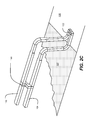
- FIG. 1 is a perspective view of a receptacle 100 for connecting to a plug of a connector 150 , according to one embodiment.
- the receptacle 100 connects electrical paths of the connector 150 to an electronic device including a printed circuit board (PCB) 130 .
- the receptacle 100 includes, among other components, a first contact 102 , a second contact 104 , an insulating member 112 , a first conductive bridge 122 , and a second conductive bridge 124 .
- the receptacle 100 includes additional contacts which are omitted in FIG. 1 to simplify the explanation.
- the first contact 102 and the second contact 104 transmit signals from the connector 150 to the PCB 130 of the electronic device.
- the first contact 102 and the second contact 104 can be implemented using metal traces.
- the first contact 102 is on a first side (i.e., top-side) of the insulating member 112 and the second contact 104 is on a second side (i.e., bottom-side) of the insulating member 112 .
- the first contact 102 and the second contact 104 extend to the PCB 130 of the electronic device.
- the first contact 102 includes a first portion 162 A extending on the first side (i.e., top-side) of the insulating member 112 at a first height 164 from a PCB surface 132 and parallel to the first side of the insulating member 112 .
- the first contact 102 further includes a second portion 162 B extending to the PCB 130 parallel to the first side of the insulating member 112 at a second height 166 from the PCB surface 132 lower than the first height 164 .
- the second height 166 from the PCB surface 132 is zero (i.e., the second portion 162 B is on the PCB surface 132 ).
- the first contact 102 includes a third portion 162 C connecting the first portion 162 A and the second portion 162 B of the first contact 102 .
- the second contact 104 includes a first portion 172 A at a third height 174 from the PCB surface 132 and parallel to the second side (i.e., bottom-side) of the insulating member 112 , a second portion 172 B extending to the PCB 130 parallel to the second side of the insulating member 112 at a fourth height 176 from the PCB surface 132 lower than the third height 174 , and a third portion 172 C connecting the first portion 172 A and the second portion 172 B of the second contact 104 .
- the third height 174 is lower than the first height 164 and higher than the second height 166
- the fourth height 176 and the second height 166 are substantially the same.
- the fourth height 176 from the PCB surface 132 is zero (i.e., the second portion 172 B is on the PCB surface 132 .
- the insulating member 112 separates the first contact 102 and the second contact 102 within the receptacle 100 .
- the insulating member 112 has a sheet-like structure and separates a first side (e.g., top-half) of the receptacle 100 from a second side (e.g., bottom-half) of the receptacle 100 .
- the insulating member 112 prevents signals transmitted via contacts (e.g., first contact 102 ) at one side (e.g., top-side) of the insulating member 112 from affecting signals transmitted via contacts (e.g., second contact 104 ) at another side (e.g., bottom-side) of the insulating member 112 .
- the insulating member 112 is an insulative plastic or any other composite material.
- the connector 150 engages with the receptacle 100 in each of two orientations. That is, the connector 150 may engage with the receptacle 100 in a first orientation while the connector 150 may also engage with the receptacle 100 in a second orientation rotated 180 degrees relative to the first orientation without reconfiguration. Conductive bridges are provided in the receptacle 100 so that plug contacts of the connector 150 may engage with the appropriate contacts of the receptacle 100 in either orientation.
- the first conductive bridge 122 connects the first contact 102 and the second contact 104 at a first location closer to the PCB 130 than the connector 150 . Specifically, the first conductive bridge 122 connects the second portion 162 B of the first contact 102 and the second portion 172 B of the second contact 104 . In one embodiment, the first conductive bridge 122 height (not shown) from the PCB surface 132 is zero (i.e., the first conductive bridge 122 is on the PCB surface 132 ). The first conductive bridge 122 is not connected to the connector 150 and acts as an open stub in the receptacle 100 . The open stub causes undesirable capacitance between the first contact 102 and the second contact 104 which in turn causes crosstalk between a signal transmitted on the first contact 102 and the second contact 104 .
- the receptacle 100 also includes the second conductive bridge 124 to reduce the capacitance introduced by the open stub which in turn reduces the crosstalk between the signal transmitted on the first contact 102 and the second contact 104 .
- the second conductive bridge 124 connects the first contact 102 and the second contact 104 at a second location closer to the connector 150 than the first conductive bridge 122 . Specifically, the second conductive bridge 124 connects the first portion 162 A of the first contact 102 and the first portion 172 A of the second contact 104 .
- the second conductive bridge 124 is formed to penetrate the insulating member 112 and the first conductive bridge 122 is separated away from the insulating member 112 .
- the second conductive bridge 124 includes a first portion 142 A extending from the first portion 162 A of the first contact 102 into the insulating member 112 , a second portion 142 B extending from the first portion 172 A of the second contact 104 into the insulating member 112 , and a first conductive bridge 144 extending between the first portion 142 A and the second portion 142 B.
- the first conductive bridge 144 extends from the first portion 142 A to the second portion 142 B and is parallel to the top or bottom surface of the insulating member 112 .
- the second conductive bridge 124 is not limited to the structure illustrated in FIG. 1 .
- the first conductive bridge 122 and the second conductive bridge 124 are separated by a distance along the path of the signals. As illustrated in FIG. 1 , the distance is the sum of length 134 A, length 134 B, and length 134 C. The distance between the first conductive bridge 122 and the second conductive bridge 124 is less than 15 mm/ ⁇ square root over ( ⁇ r ) ⁇ where ⁇ r represents the relative permittivity of the insulating member 112 . If the distance between the first conductive bridge 122 and the second conductive bridge 124 is greater than 15 mm/ ⁇ square root over ( ⁇ r ) ⁇ , the bandwidth is limited and signal quality degrades.
- the distance between the first conductive bridge 122 and the second conductive bridge 124 is less than 15 mm/ ⁇ square root over ( ⁇ r ) ⁇ . In the embodiment where the insulating member 112 is air, the distance between the first conductive bridge 122 and the second conductive bridge 124 is less than 15 mm.
- FIG. 2A is a perspective view of the receptacle 100 illustrating the connector 150 in the first orientation where a first plug contact 152 of the connector 150 is connected to first contact 102 of the receptacle 100 , according to one embodiment.
- FIG. 2A illustrates the same embodiment of the receptacle 100 illustrated in FIG. 1 with the connector 150 engaging with the receptacle 100 in the first orientation.
- the first contact 102 at the first side (i.e., top side) of the receptacle 100 electrically couples with the first plug contact 152 when the connector 150 engages with the receptacle 100 in the first orientation.
- the receptacle 100 transmits a signal from the first plug contact 152 of the connector 150 to the PCB 130 of the electronic device via the first conductive bridge 122 and the second conductive bridge 124 .
- FIG. 2B is a perspective view of the receptacle 100 illustrating the connector 150 in a second orientation where the first plug contact 152 of the connector 150 is connected to the second contact 104 of the receptacle 100 , according to one embodiment.
- FIG. 2B illustrates the same embodiment of the receptacle 100 illustrated in FIG. 1 with the connector 150 engaging with the receptacle 100 in the second orientation. That is, FIG. 2B illustrates the same embodiment as FIG. 2A but with the orientation of the connector 150 reversed.
- the second contact 104 at the second side (i.e., bottom side) of the receptacle 100 electrically couples with the first plug contact 152 when the connector 150 engages with the receptacle 100 in the second orientation.
- the receptacle 100 transmits a signal from the first plug contact 152 of the connector 150 to the PCB 130 of the electronic device via the first conductive bridge 122 and the second conductive bridge 124 .
- FIG. 2C is a perspective view of first and second contacts 102 , 104 of the receptacle and first and second conductive bridges 122 , 144 connecting these contacts, according to one embodiment.
- the first and second contacts 102 , 104 extend parallel along a PCB surface 132 , extends vertically down towards the PCB 130 .
- the first conductive bridge 122 is located closer to the PCB 130 than the second conductive bridge 144 .
- FIG. 2D is a front view of the receptacle mounted on the PCB 130 , according to one embodiment.
- the first plug contact 152 is shown in FIG. 2D as coming into contact with the first contact 120 .
- FIG. 3 illustrates a perspective view of a receptacle 300 for connecting to a first plug contact 352 and a second plug contact 354 of a connector 350 , according to one embodiment.
- the receptacle 300 of FIG. 3 includes a total of four contacts (e.g., first contact 302 , second contact 304 , third contact 306 and fourth contact 308 ) for connecting the first plug contact 352 and the second plug contact 354 of the connector 350 when the connector 350 engages in the first orientation or the second orientation.
- the receptacle 300 connects multiple electrical paths of the connector 350 to a PCB 330 of an electronic device.
- the receptacle 300 , the connector 350 , and the PCB 330 are similar to the receptacle 100 , the connector 350 , and the PCB 130 of FIG. 1 , respectively.
- the receptacle 300 of FIG. 3 includes a third contact 306 and a fourth contact 308 , a third conductive bridge 326 and a fourth conductive bridge 328 .
- the receptacle 300 includes additional contacts which are omitted in FIG. 3 to simplify the explanation.
- the first contact 302 , the second contact 304 , the third contact 306 , and the fourth contact 308 transmit signals from the connector 350 to the PCB 330 of the electronic device.
- the contacts 302 through 308 can be implemented using metal traces.
- the first contact 302 and the third contact 306 are on the first side (i.e., top-side) of the insulating member 312 and the second contact 304 and the fourth contact 308 are on the second side (i.e., bottom-side) of the insulating member.
- the contacts 302 through 308 extend to the PCB 330 of the electronic device.
- the receptacle 300 is a Universal Serial Bus (USB) Type C receptacle.
- the USB Type C receptacle is a receptacle 300 which conforms to the mechanical and electrical requirements of the USB Type C standard developed and maintained by the Universal Serial Bus Implementers Forum (USB-IF).
- the receptacle 300 complying with the USB Type C standard includes additional contacts which are omitted in FIG. 3 for the sake of convenience.
- the first contact 302 and the third contact 306 carry differential data signals and some single-ended signals when the connector 350 engages with the receptacle 300 in the first orientation.
- the second contact 304 and the fourth contact 308 carry differential data signals and some single-ended signals when the connector 350 engages with the receptacle 300 in the second orientation.
- the first contact 302 and the second contact 304 are similar to the first contact 102 and the second contact 104 illustrated in FIG. 1 .
- the first contact 302 includes a first portion 362 A at a first height 364 from a PCB surface 332 and parallel to the first side (i.e., bottom-side) of the insulating member 312 , a second portion 362 B extending to the PCB 330 parallel to the first side of the insulating member 112 at a second height 366 from the PCB surface 332 lower than the first height 364 , and a third portion 362 C connecting the first portion 362 A and the second portion 362 B of the first contact 302 .
- the second height 366 from the PCB surface 332 is zero (i.e., the second portion 362 B is on the PCB surface 332 ).
- the second contact 304 includes a first portion 372 A at a third height 374 from the PCB surface 332 and parallel to the second side (i.e., bottom-side) of the insulating member 312 , a second portion 372 B extending to the PCB 330 parallel to the second side of the insulating member 312 at a fourth height 376 from the PCB surface 332 lower than the third height 374 , and a third portion 372 C connecting the first portion 372 A and the second portion 372 B of the second contact 304 .
- the fourth height 376 from the PCB surface 332 is zero (i.e., the second portion 372 B is on the PCB surface 332 ).
- the third contact 306 includes a first portion 382 A extending on the first side (i.e., top-side) of the insulating member 312 at a fifth height 384 from the PCB surface 332 and parallel to the first side of the insulating member 312 , a second portion 382 B extending to the PCB 330 parallel to the first side of the insulating member 312 at a sixth height 386 from the PCB surface 332 lower than the fifth height 384 , and a third portion 382 C connecting the first portion 382 A and the second portion 382 B of the third contact 306 .
- the fifth height 384 and the first height 364 are substantially the same
- the sixth height 386 and the second height 376 are substantially the same.
- the sixth height 386 from the PCB surface 332 is zero (i.e., the second portion 382 B is on the PCB surface 332 ).
- the fourth contact 308 includes a first portion 392 A extending on the second side (i.e., bottom-side) of the insulating member 312 at a seventh height 394 from the PCB surface 332 and parallel to the second side of the insulating member 312 , a second portion 392 B extending to the PCB 330 parallel to the second side of the insulating member 312 at an eighth height 396 from the PCB surface 332 lower than the seventh height 394 , and a third portion 392 C connecting the first portion 392 A and the second portion 392 B of the fourth contact 308 .
- the seventh height 394 and the third height 374 are substantially the same
- the eighth height 396 and the fourth height 366 are substantially the same.
- the eighth height 396 from the PCB surface 332 is zero (i.e., the second portion 392 B is no the PCB surface 332 ).
- the insulating member 312 is similar to the insulating member 112 of the receptacle 100 illustrated in FIG. 1 .
- the insulating member 312 separates the first contact 302 and the third contact 306 from the second contact 304 and the fourth contact 308 within the receptacle 300 .
- the insulating member 312 has a similar structure as the insulating member 112 of the receptacle 100 .
- the insulating member 312 is an insulative plastic or any other composite material.
- the connector 350 engages with the receptacle in each of the two orientations.
- Conductive bridges are provided in the receptacle 300 so that plug contacts of the connector 350 may engage with the appropriate contacts of the receptacle 300 in either orientation.
- the first conductive bridge 322 connects the first contact 302 and the second contact 304 at a first location closer to the PCB 330 than the connector 350 .
- the first conductive bridge 322 connects the second portion 362 B of the first contact 302 and the second portion 372 B of the second contact 104 .
- the third conductive bridge 326 connects the third contact 306 and the fourth contact 308 at a third location closer to the PCB 330 than the connector 350 .
- the third conductive bridge 326 connects the second portion 382 B of the third contact 306 and the second portion 392 B of the fourth contact 308 .
- the first conductive bridge 322 and the third conductive bridge 326 are also separated by a distance along the path of the signal.
- the first conductive bridge 322 height (not shown) from the PCB surface 332 is zero (i.e., the first conductive bridge 322 is on the PCB surface 332 ).
- the second conductive bridge 326 height (not shown) form the PCB surface 332 is zero (i.e., the second conductive bridge 326 is on the PCB surface 332 ).
- the third location of the third conductive bridge 326 and the first location of the first conductive bridge 322 are substantially the same.
- the first conductive bridge 322 and the third conductive bridge 326 are not connected to the connector 350 and act as open stubs in the receptacle 300 . The open stubs limit the bandwidth and degrade the signal quality of the signal transmitted via the contacts 302 through 308 .
- the second conductive bridge 324 and the fourth conductive bridge 328 reduce the effect of the open stubs.
- the second conductive bridge 324 connects the first contact 302 and the second contact 304 at a second location closer to the connector 350 than the first conductive bridge 322 .
- the fourth conductive bridge 328 connects the third contact 306 and the fourth contact 308 at a fourth location closer to the connector 350 than the third conductive bridge 326 .
- the second conductive bridge 324 and the fourth conductive bridge 328 are spatially separated from one another by a distance 336 . In one embodiment, the second location of the second conductive bridge 324 and the fourth location of the fourth conductive bridge 328 are substantially the same.
- the second conductive bridge 324 and the fourth conductive bridge 328 are formed to penetrate the insulating member 312 and the first conductive bridge 322 and the third conductive bridge 326 are separated away from the insulating member 312 .
- the fourth conductive bridge 328 includes a first portion 346 A extending from the first portion 382 A of the third contact 306 into the insulating member 312 , a second portion 346 B extending from the first portion 392 A of the fourth contact 308 into the insulating member 312 , and a second conductive bridge 348 extending between the first portion 346 A and the second portion 346 B.
- the second conductive bridge 348 extends from the first portion 346 A to the second portion 346 B and is parallel to the top or bottom surface of the insulating member 312 .
- the second conductive bridge 324 and the fourth conductive bridge 328 are not limited to the structure illustrated in FIG. 3 .
- the third conductive bridge 326 and the fourth conductive bridge 328 are separated by a distance. As illustrated in FIG. 3 , the distance is the sum of lengths 336 A, 336 B, and 336 C. The distance between the third conductive bridge 326 and the fourth conductive bridge 328 is less than 15 mm/ ⁇ square root over ( ⁇ r ) ⁇ where ⁇ r represents the relative permittivity of the insulating member 112 . The distance between the first conductive bridge 322 and the second conductive bridge 324 is less than the distance between the third conductive bridge 326 and the fourth conductive bridge 328 .
- FIG. 4A is a perspective view of the receptacle 300 illustrating the connector 350 in the first orientation where a first plug contact 352 and a second plug contact 354 of the connector 350 are connected to the first contact 302 and third contact 306 of the receptacle 300 , respectively.
- FIG. 4A illustrates the same embodiment of the receptacle illustrated in FIG. 3 with the connector 350 engaging the receptacle 300 in the first orientation.
- the first contact 302 and the third contact 306 at the first side (i.e., top side) of the receptacle 300 electrically couple with the first plug contact 352 and the second plug contact 354 , respectively, when the connector 350 engages with the receptacle 300 in the first orientation.
- the first contact 302 and the third contact 306 transmit signals from the first plug contact 352 and the second plug contact 354 , respectively, to the PCB 330 of the electronic device via the first conductive bridge 322 , the second conductive bridge 324 , the third conductive bridge 326 , and the fourth conductive bridge 328 (hereinafter collectively referred to as “conductive bridges 322 through 328 ”).
- FIG. 4B is a perspective view of the receptacle 300 illustrating the connector 350 in the second orientation where the first plug contact 352 and the second plug contact 354 of the connector 350 are connected to the second contact 304 and fourth contact 308 of the receptacle 300 , respectively.
- FIG. 4B illustrates the same embodiment of the receptacle 300 illustrated in FIG. 3 with the connector 350 engaging with the receptacle 300 in the second orientation. That is FIG. 4B illustrates the same embodiment as FIG. 4A but with the orientation of the connector 350 reversed.
- the second contact 304 and the fourth contact 308 at the second side (i.e., bottom side) of the receptacle 300 electrically couple with the first plug contact 352 and the second plug contact 354 , respectively, when the connector 350 engages with the receptacle 300 in the second orientation.
- the second contact 304 and the fourth contact 308 transmit signals from the first plug contact 352 and the second plug contact 354 , respectively, to the PCB 130 of the electronic device via the conductive bridges 322 through 328 .
Abstract
Description
Claims (20)
Priority Applications (4)
| Application Number | Priority Date | Filing Date | Title |
|---|---|---|---|
| US14/824,717 US9472873B1 (en) | 2015-08-12 | 2015-08-12 | Reversible receptacle connector |
| DE112016003680.9T DE112016003680B4 (en) | 2015-08-12 | 2016-06-16 | Reversible socket connector |
| CN201680045483.4A CN107925202B (en) | 2015-08-12 | 2016-06-16 | Socket connector may be reversed |
| PCT/US2016/037937 WO2017027102A1 (en) | 2015-08-12 | 2016-06-16 | Reversible receptacle connector |
Applications Claiming Priority (1)
| Application Number | Priority Date | Filing Date | Title |
|---|---|---|---|
| US14/824,717 US9472873B1 (en) | 2015-08-12 | 2015-08-12 | Reversible receptacle connector |
Publications (1)
| Publication Number | Publication Date |
|---|---|
| US9472873B1 true US9472873B1 (en) | 2016-10-18 |
Family
ID=57120540
Family Applications (1)
| Application Number | Title | Priority Date | Filing Date |
|---|---|---|---|
| US14/824,717 Active US9472873B1 (en) | 2015-08-12 | 2015-08-12 | Reversible receptacle connector |
Country Status (4)
| Country | Link |
|---|---|
| US (1) | US9472873B1 (en) |
| CN (1) | CN107925202B (en) |
| DE (1) | DE112016003680B4 (en) |
| WO (1) | WO2017027102A1 (en) |
Cited By (2)
| Publication number | Priority date | Publication date | Assignee | Title |
|---|---|---|---|---|
| US10559932B2 (en) * | 2010-07-19 | 2020-02-11 | Chou Hsien Tsai | Bidirectional duplex electrical connector having circuit board |
| US11035882B2 (en) * | 2018-10-26 | 2021-06-15 | Samsung Electronics Co., Ltd. | Signal transfer structure for test equipment and automatic test apparatus for testing semiconductor devices using the same |
Citations (42)
| Publication number | Priority date | Publication date | Assignee | Title |
|---|---|---|---|---|
| US4116525A (en) * | 1977-01-27 | 1978-09-26 | Automatic Equipment Development Corporation | Electrical connector assembly |
| US4367907A (en) * | 1980-08-04 | 1983-01-11 | Magnetic Controls Company | Circuit monitoring jack |
| US4602830A (en) * | 1984-09-20 | 1986-07-29 | Amp Incorporated | Double row electrical connector |
| US5647765A (en) * | 1995-09-12 | 1997-07-15 | Regal Electronics, Inc. | Shielded connector with conductive gasket interface |
| US5915989A (en) * | 1997-05-19 | 1999-06-29 | Lucent Technologies Inc. | Connector with counter-balanced crosswalk compensation scheme |
| US5964610A (en) * | 1997-12-31 | 1999-10-12 | Dekko Engineering, Inc. | Reversible power entry |
| US6238250B1 (en) * | 1999-12-29 | 2001-05-29 | Siecor Operations, Llc | In-jack shunt connections and methods therefor |
| US6558203B2 (en) * | 2001-07-10 | 2003-05-06 | Alan L. Pocrass | Multi-function RJ-type modular connector |
| US6595805B2 (en) * | 2001-07-10 | 2003-07-22 | Alan L. Pocrass | Dual function RJ connector |
| US6866527B2 (en) * | 1999-08-23 | 2005-03-15 | Patrick Potega | Connector assembly for electrical signal transfer among multiple devices |
| US6935879B2 (en) * | 2001-07-10 | 2005-08-30 | Littelfuse, Inc. | Connectors having circuit protection |
| US20060024997A1 (en) * | 2004-08-02 | 2006-02-02 | M-Systems Flash Disk Pioneers Ltd. | Reversible universal serial bus (USB) device and connector |
| US7361059B2 (en) * | 2003-07-28 | 2008-04-22 | Sandisk Secure Content Solutions, Inc | Electrical connector |
| US20080119076A1 (en) * | 2006-11-22 | 2008-05-22 | Sandisk Il Ltd. | Systems of reliably interconnectable reversible usb connectors |
| US20080119291A1 (en) * | 2006-11-17 | 2008-05-22 | Nintendo Co., Ltd. | Secure and/or lockable connecting arrangement for video game system |
| US7416419B2 (en) * | 2006-08-16 | 2008-08-26 | Sandisk Corporation | Methods for ESD protection |
| US20080248662A1 (en) * | 2006-02-10 | 2008-10-09 | Leviton Manufacturing Co., Inc. | Tamper resistant interrupter receptacle having a detachable metal skin |
| US20080311781A1 (en) * | 2007-06-12 | 2008-12-18 | Panduit Corp. | Multi-Position Quick Release Plug Cassette Assembly |
| US7581967B2 (en) * | 2006-08-16 | 2009-09-01 | Sandisk Corporation | Connector with ESD protection |
| US7601034B1 (en) * | 2008-05-07 | 2009-10-13 | Ortronics, Inc. | Modular insert and jack including moveable reactance section |
| US7682169B2 (en) * | 2007-12-17 | 2010-03-23 | Hyundai Motor Company | Bidirectional USB port for vehicle |
| US7708566B2 (en) * | 2007-10-30 | 2010-05-04 | Hon Hai Precision Ind. Co., Ltd. | Electrical connector with integrated circuit bonded thereon |
| US7824222B2 (en) * | 2007-06-29 | 2010-11-02 | Hosiden Corporation | Connector |
| US7963773B2 (en) * | 2007-12-24 | 2011-06-21 | Craig Palli | Magnetic and locking cable connectors |
| US8021183B2 (en) * | 2008-10-31 | 2011-09-20 | Apple Inc. | Cold headed electric plug arm |
| US20110294354A1 (en) * | 2010-05-25 | 2011-12-01 | I/O Interconnect, Ltd. | Usb port, usb plug, and connection structure thereof |
| US20120015561A1 (en) * | 2010-07-19 | 2012-01-19 | Chou Hsien Tsai | Electrical connector |
| US8125748B2 (en) * | 2007-11-20 | 2012-02-28 | Zhejiang Kedu Electric Mfg. Co. Ltd. | Ground fault circuit interrupter |
| US8152558B2 (en) * | 2007-11-13 | 2012-04-10 | Tyco Electronics Belgium Ec Nv | Shielded USB connector system |
| US8198563B2 (en) * | 2009-04-15 | 2012-06-12 | Chou Hsien Tsai | Socket structure with duplex electrical connection |
| US20130005193A1 (en) * | 2011-06-30 | 2013-01-03 | Chou Hsien Tsai | Duplex male electrical connector with socket shell |
| US20130095702A1 (en) * | 2010-06-21 | 2013-04-18 | Apple Inc. | External contact plug connector |
| US8517751B1 (en) * | 2010-05-28 | 2013-08-27 | Apple Inc. | Dual orientation connector with external contacts and conductive frame |
| US8782869B2 (en) * | 2011-05-17 | 2014-07-22 | Apple Inc. | Unlocking tool for male connector |
| US20140206209A1 (en) * | 2013-01-24 | 2014-07-24 | Apple Inc. | Reversible usb connector |
| US8911262B1 (en) * | 2013-12-09 | 2014-12-16 | Google Inc. | Electrical receptacle with lower speed signaling contacts farther from center |
| US8911260B2 (en) * | 2010-06-21 | 2014-12-16 | Apple Inc. | External contact plug connector |
| US8944827B2 (en) * | 2012-03-13 | 2015-02-03 | Dai-Ichi Seiko Co., Ltd. | Coaxial electrical connector and coaxial electrical connector device |
| US9024581B2 (en) * | 2008-05-21 | 2015-05-05 | James W. McGinley | Charger plug with improved package |
| US9033739B2 (en) * | 2011-09-09 | 2015-05-19 | Apple Inc. | Techniques for shielding connectors that allow for conformal coating against corrosion |
| US9231344B1 (en) * | 2014-09-01 | 2016-01-05 | Sheng-Hsin Liao | Double-sided USB connector structure having a spring mechanism supporting an insulating body with plurality of terminals on two surfaces of the insulating body |
| US9231356B1 (en) * | 2014-07-15 | 2016-01-05 | Lotes Co., Ltd. | Electrical connector for transferring high frequency signal |
Family Cites Families (9)
| Publication number | Priority date | Publication date | Assignee | Title |
|---|---|---|---|---|
| JPH052392U (en) * | 1991-06-27 | 1993-01-14 | 日本電気株式会社 | Surface mount connector |
| US6244904B1 (en) * | 1998-01-16 | 2001-06-12 | The Whitaker Corporation | Electrical connector for attaching conductors to speaker leads |
| DE202004018757U1 (en) * | 2004-12-04 | 2006-04-13 | Weidmüller Interface GmbH & Co. KG | Device for the electrical bridging of two busbars |
| US7387539B2 (en) | 2006-04-14 | 2008-06-17 | Rodney J. Trenne | Reversible universal serial bus connection interface for USB connectors and universal serial bus ports |
| SG186504A1 (en) * | 2011-06-10 | 2013-01-30 | Tyco Electronics Singapore Pte Ltd | Cross talk reduction for a high speed electrical connector |
| JP5717567B2 (en) * | 2011-07-14 | 2015-05-13 | 日本モレックス合同会社 | Cable assembly, connector and semiconductor test equipment |
| CN103036085A (en) * | 2011-10-10 | 2013-04-10 | 富泰华工业(深圳)有限公司 | Connector with double plug-in faces |
| JP6166040B2 (en) * | 2012-12-28 | 2017-07-19 | 日本航空電子工業株式会社 | connector |
| CN204103121U (en) * | 2014-09-11 | 2015-01-14 | 增城市兴禾旺塑胶五金电子厂 | A kind of can the USB socket connector of double-side plug-in |
-
2015
- 2015-08-12 US US14/824,717 patent/US9472873B1/en active Active
-
2016
- 2016-06-16 WO PCT/US2016/037937 patent/WO2017027102A1/en active Application Filing
- 2016-06-16 DE DE112016003680.9T patent/DE112016003680B4/en active Active
- 2016-06-16 CN CN201680045483.4A patent/CN107925202B/en active Active
Patent Citations (45)
| Publication number | Priority date | Publication date | Assignee | Title |
|---|---|---|---|---|
| US4116525A (en) * | 1977-01-27 | 1978-09-26 | Automatic Equipment Development Corporation | Electrical connector assembly |
| US4367907A (en) * | 1980-08-04 | 1983-01-11 | Magnetic Controls Company | Circuit monitoring jack |
| US4602830A (en) * | 1984-09-20 | 1986-07-29 | Amp Incorporated | Double row electrical connector |
| US5647765A (en) * | 1995-09-12 | 1997-07-15 | Regal Electronics, Inc. | Shielded connector with conductive gasket interface |
| US5915989A (en) * | 1997-05-19 | 1999-06-29 | Lucent Technologies Inc. | Connector with counter-balanced crosswalk compensation scheme |
| US5964610A (en) * | 1997-12-31 | 1999-10-12 | Dekko Engineering, Inc. | Reversible power entry |
| US6866527B2 (en) * | 1999-08-23 | 2005-03-15 | Patrick Potega | Connector assembly for electrical signal transfer among multiple devices |
| US6238250B1 (en) * | 1999-12-29 | 2001-05-29 | Siecor Operations, Llc | In-jack shunt connections and methods therefor |
| US6558203B2 (en) * | 2001-07-10 | 2003-05-06 | Alan L. Pocrass | Multi-function RJ-type modular connector |
| US6595805B2 (en) * | 2001-07-10 | 2003-07-22 | Alan L. Pocrass | Dual function RJ connector |
| US6935879B2 (en) * | 2001-07-10 | 2005-08-30 | Littelfuse, Inc. | Connectors having circuit protection |
| US7361059B2 (en) * | 2003-07-28 | 2008-04-22 | Sandisk Secure Content Solutions, Inc | Electrical connector |
| US20060024997A1 (en) * | 2004-08-02 | 2006-02-02 | M-Systems Flash Disk Pioneers Ltd. | Reversible universal serial bus (USB) device and connector |
| US20080248662A1 (en) * | 2006-02-10 | 2008-10-09 | Leviton Manufacturing Co., Inc. | Tamper resistant interrupter receptacle having a detachable metal skin |
| US20090286411A1 (en) * | 2006-02-10 | 2009-11-19 | Leviton Manufacturing Co. Inc. | Tamper resistant interrupter receptacle having a detachable metal skin |
| US7416419B2 (en) * | 2006-08-16 | 2008-08-26 | Sandisk Corporation | Methods for ESD protection |
| US7581967B2 (en) * | 2006-08-16 | 2009-09-01 | Sandisk Corporation | Connector with ESD protection |
| US20080119291A1 (en) * | 2006-11-17 | 2008-05-22 | Nintendo Co., Ltd. | Secure and/or lockable connecting arrangement for video game system |
| US7537471B2 (en) * | 2006-11-22 | 2009-05-26 | Sandisk Il, Ltd. | Systems of reliably interconnectable reversible USB connectors |
| US20080119076A1 (en) * | 2006-11-22 | 2008-05-22 | Sandisk Il Ltd. | Systems of reliably interconnectable reversible usb connectors |
| US20080311781A1 (en) * | 2007-06-12 | 2008-12-18 | Panduit Corp. | Multi-Position Quick Release Plug Cassette Assembly |
| US7824222B2 (en) * | 2007-06-29 | 2010-11-02 | Hosiden Corporation | Connector |
| US7708566B2 (en) * | 2007-10-30 | 2010-05-04 | Hon Hai Precision Ind. Co., Ltd. | Electrical connector with integrated circuit bonded thereon |
| US8152558B2 (en) * | 2007-11-13 | 2012-04-10 | Tyco Electronics Belgium Ec Nv | Shielded USB connector system |
| US8125748B2 (en) * | 2007-11-20 | 2012-02-28 | Zhejiang Kedu Electric Mfg. Co. Ltd. | Ground fault circuit interrupter |
| US7682169B2 (en) * | 2007-12-17 | 2010-03-23 | Hyundai Motor Company | Bidirectional USB port for vehicle |
| US7963773B2 (en) * | 2007-12-24 | 2011-06-21 | Craig Palli | Magnetic and locking cable connectors |
| US7601034B1 (en) * | 2008-05-07 | 2009-10-13 | Ortronics, Inc. | Modular insert and jack including moveable reactance section |
| US9024581B2 (en) * | 2008-05-21 | 2015-05-05 | James W. McGinley | Charger plug with improved package |
| US8021183B2 (en) * | 2008-10-31 | 2011-09-20 | Apple Inc. | Cold headed electric plug arm |
| US8198563B2 (en) * | 2009-04-15 | 2012-06-12 | Chou Hsien Tsai | Socket structure with duplex electrical connection |
| US20110294354A1 (en) * | 2010-05-25 | 2011-12-01 | I/O Interconnect, Ltd. | Usb port, usb plug, and connection structure thereof |
| US8517751B1 (en) * | 2010-05-28 | 2013-08-27 | Apple Inc. | Dual orientation connector with external contacts and conductive frame |
| US20130095702A1 (en) * | 2010-06-21 | 2013-04-18 | Apple Inc. | External contact plug connector |
| US8911260B2 (en) * | 2010-06-21 | 2014-12-16 | Apple Inc. | External contact plug connector |
| US20120015561A1 (en) * | 2010-07-19 | 2012-01-19 | Chou Hsien Tsai | Electrical connector |
| US9142926B2 (en) * | 2010-07-19 | 2015-09-22 | Chou Hsien Tsai | Electrical connector for bidirectional plug insertion |
| US8782869B2 (en) * | 2011-05-17 | 2014-07-22 | Apple Inc. | Unlocking tool for male connector |
| US20130005193A1 (en) * | 2011-06-30 | 2013-01-03 | Chou Hsien Tsai | Duplex male electrical connector with socket shell |
| US9033739B2 (en) * | 2011-09-09 | 2015-05-19 | Apple Inc. | Techniques for shielding connectors that allow for conformal coating against corrosion |
| US8944827B2 (en) * | 2012-03-13 | 2015-02-03 | Dai-Ichi Seiko Co., Ltd. | Coaxial electrical connector and coaxial electrical connector device |
| US20140206209A1 (en) * | 2013-01-24 | 2014-07-24 | Apple Inc. | Reversible usb connector |
| US8911262B1 (en) * | 2013-12-09 | 2014-12-16 | Google Inc. | Electrical receptacle with lower speed signaling contacts farther from center |
| US9231356B1 (en) * | 2014-07-15 | 2016-01-05 | Lotes Co., Ltd. | Electrical connector for transferring high frequency signal |
| US9231344B1 (en) * | 2014-09-01 | 2016-01-05 | Sheng-Hsin Liao | Double-sided USB connector structure having a spring mechanism supporting an insulating body with plurality of terminals on two surfaces of the insulating body |
Cited By (2)
| Publication number | Priority date | Publication date | Assignee | Title |
|---|---|---|---|---|
| US10559932B2 (en) * | 2010-07-19 | 2020-02-11 | Chou Hsien Tsai | Bidirectional duplex electrical connector having circuit board |
| US11035882B2 (en) * | 2018-10-26 | 2021-06-15 | Samsung Electronics Co., Ltd. | Signal transfer structure for test equipment and automatic test apparatus for testing semiconductor devices using the same |
Also Published As
| Publication number | Publication date |
|---|---|
| WO2017027102A1 (en) | 2017-02-16 |
| DE112016003680B4 (en) | 2019-10-10 |
| CN107925202A (en) | 2018-04-17 |
| CN107925202B (en) | 2019-06-21 |
| DE112016003680T5 (en) | 2018-04-19 |
Similar Documents
| Publication | Publication Date | Title |
|---|---|---|
| US10135197B2 (en) | Electrical connector having common grounding | |
| US9214768B2 (en) | Communication connector and transmission module thereof | |
| US9306334B2 (en) | High speed plug connector having improved high frequency performance | |
| US9312641B2 (en) | Electrical connector used for transmitting high frequency signals | |
| TWI469446B (en) | Card edge connector | |
| US9093792B2 (en) | Connector and signal transmission method using the same | |
| US9711908B2 (en) | Electrical connector having improved terminals | |
| US8202120B2 (en) | High frequency socket connector | |
| US20160365673A1 (en) | Cable assembly | |
| CN104600454B (en) | Socket electric connector | |
| US9130314B2 (en) | Communication connector and terminal lead frame thereof | |
| KR101762722B1 (en) | Plug adapter | |
| US8083546B2 (en) | Electric connector and electric assembly | |
| TWI388098B (en) | Electrical connector assembly | |
| US9660386B2 (en) | High frequency RJ45 plug with non-continuous ground planes for cross talk control | |
| KR20110031911A (en) | Rf coaxial connector | |
| US8684770B2 (en) | Cable end connector and cable connector assembly having the same | |
| US20120252270A1 (en) | USB Connector | |
| CN102195223A (en) | Electrical connector and its complex | |
| CN105576407A (en) | Buckling fuzz button electric connector | |
| TWM502987U (en) | Electrical connector including fins | |
| US9472873B1 (en) | Reversible receptacle connector | |
| US9350099B2 (en) | Connector having a conductive casing with an inclined plane parallel to a section of a terminal | |
| US8070532B1 (en) | Electrical connector assembly with anti-mismatching mating connectors | |
| US7575483B1 (en) | Electrical connector having substrate having conductive trace to balance electrical couplings among terminals |
Legal Events
| Date | Code | Title | Description |
|---|---|---|---|
| AS | Assignment |
Owner name: LATTICE SEMICONDUCTOR CORPORATION, OREGON Free format text: ASSIGNMENT OF ASSIGNORS INTEREST;ASSIGNORS:JEONG, YOUCHUL;KIM, JAEMIN;SUNG, BAEGIN;AND OTHERS;REEL/FRAME:036311/0660 Effective date: 20150810 |
|
| AS | Assignment |
Owner name: JEFFERIES FINANCE LLC, NEW YORK Free format text: SECURITY INTEREST;ASSIGNOR:LATTICE SEMICONDUCTOR CORPORATION;REEL/FRAME:037925/0023 Effective date: 20151112 |
|
| STCF | Information on status: patent grant |
Free format text: PATENTED CASE |
|
| AS | Assignment |
Owner name: WELLS FARGO BANK, NATIONAL ASSOCIATION, AS ADMINIS Free format text: SECURITY INTEREST;ASSIGNOR:LATTICE SEMICONDUCTOR CORPORATION;REEL/FRAME:049795/0481 Effective date: 20190718 Owner name: WELLS FARGO BANK, NATIONAL ASSOCIATION, AS ADMINISTRATIVE AGENT, COLORADO Free format text: SECURITY INTEREST;ASSIGNOR:LATTICE SEMICONDUCTOR CORPORATION;REEL/FRAME:049795/0481 Effective date: 20190718 |
|
| MAFP | Maintenance fee payment |
Free format text: PAYMENT OF MAINTENANCE FEE, 4TH YEAR, LARGE ENTITY (ORIGINAL EVENT CODE: M1551); ENTITY STATUS OF PATENT OWNER: LARGE ENTITY Year of fee payment: 4 |
|
| AS | Assignment |
Owner name: LATTICE SEMICONDUCTOR CORPORATION, OREGON Free format text: RELEASE BY SECURED PARTY;ASSIGNOR:JEFFERIES FINANCE LLC;REEL/FRAME:058013/0427 Effective date: 20211103 |
|
| AS | Assignment |
Owner name: LATTICE SEMICONDUCTOR CORPORATION, OREGON Free format text: RELEASE BY SECURED PARTY;ASSIGNOR:WELLS FARGO BANK, NATIONAL ASSOCIATION, AS ADMINISTRATIVE AGENT;REEL/FRAME:058067/0896 Effective date: 20211109 |
|
| AS | Assignment |
Owner name: UNIVERSAL CONNECTIVITY TECHNOLOGIES INC., DELAWARE Free format text: ASSIGNMENT OF ASSIGNORS INTEREST;ASSIGNOR:LATTICE SEMICONDUCTOR CORPORATION;REEL/FRAME:058979/0440 Effective date: 20211116 |
|
| MAFP | Maintenance fee payment |
Free format text: PAYMENT OF MAINTENANCE FEE, 8TH YEAR, LARGE ENTITY (ORIGINAL EVENT CODE: M1552); ENTITY STATUS OF PATENT OWNER: LARGE ENTITY Year of fee payment: 8 |