US9460576B2 - Capacitive fingerprint sensing device with demodulation circuitry in sensing element - Google Patents
Capacitive fingerprint sensing device with demodulation circuitry in sensing element Download PDFInfo
- Publication number
- US9460576B2 US9460576B2 US14/812,480 US201514812480A US9460576B2 US 9460576 B2 US9460576 B2 US 9460576B2 US 201514812480 A US201514812480 A US 201514812480A US 9460576 B2 US9460576 B2 US 9460576B2
- Authority
- US
- United States
- Prior art keywords
- sensing
- signal
- potential
- circuitry
- providing
- Prior art date
- Legal status (The legal status is an assumption and is not a legal conclusion. Google has not performed a legal analysis and makes no representation as to the accuracy of the status listed.)
- Active
Links
- 230000005284 excitation Effects 0.000 claims abstract description 105
- 230000008859 change Effects 0.000 claims abstract description 54
- 230000001681 protective effect Effects 0.000 claims abstract description 9
- 238000005259 measurement Methods 0.000 claims description 61
- 239000003990 capacitor Substances 0.000 claims description 24
- 239000000758 substrate Substances 0.000 claims description 24
- 230000007704 transition Effects 0.000 claims description 24
- 230000003071 parasitic effect Effects 0.000 claims description 17
- 239000004065 semiconductor Substances 0.000 claims description 13
- 238000000034 method Methods 0.000 claims description 10
- 230000001747 exhibiting effect Effects 0.000 claims description 2
- 230000004913 activation Effects 0.000 description 20
- 238000005070 sampling Methods 0.000 description 18
- 239000010410 layer Substances 0.000 description 12
- 238000010586 diagram Methods 0.000 description 10
- 239000011253 protective coating Substances 0.000 description 8
- 230000001276 controlling effect Effects 0.000 description 7
- 238000002955 isolation Methods 0.000 description 7
- 230000003111 delayed effect Effects 0.000 description 6
- 238000004891 communication Methods 0.000 description 5
- 230000000875 corresponding effect Effects 0.000 description 4
- 238000013461 design Methods 0.000 description 4
- 238000005265 energy consumption Methods 0.000 description 4
- 230000008878 coupling Effects 0.000 description 3
- 238000010168 coupling process Methods 0.000 description 3
- 238000005859 coupling reaction Methods 0.000 description 3
- 238000001914 filtration Methods 0.000 description 3
- 230000006870 function Effects 0.000 description 3
- 239000002184 metal Substances 0.000 description 3
- 238000012545 processing Methods 0.000 description 3
- 230000002238 attenuated effect Effects 0.000 description 2
- 230000008901 benefit Effects 0.000 description 2
- 230000001419 dependent effect Effects 0.000 description 2
- 230000003287 optical effect Effects 0.000 description 2
- 230000008569 process Effects 0.000 description 2
- 230000009467 reduction Effects 0.000 description 2
- 230000003213 activating effect Effects 0.000 description 1
- 230000003321 amplification Effects 0.000 description 1
- 230000005540 biological transmission Effects 0.000 description 1
- 238000000576 coating method Methods 0.000 description 1
- 238000004590 computer program Methods 0.000 description 1
- 230000002596 correlated effect Effects 0.000 description 1
- 230000000694 effects Effects 0.000 description 1
- 239000011521 glass Substances 0.000 description 1
- 230000006872 improvement Effects 0.000 description 1
- 238000012986 modification Methods 0.000 description 1
- 230000004048 modification Effects 0.000 description 1
- 238000003199 nucleic acid amplification method Methods 0.000 description 1
- 230000002093 peripheral effect Effects 0.000 description 1
- 239000011241 protective layer Substances 0.000 description 1
- 230000000630 rising effect Effects 0.000 description 1
- 238000006748 scratching Methods 0.000 description 1
- 230000002393 scratching effect Effects 0.000 description 1
- 238000007493 shaping process Methods 0.000 description 1
- 230000001360 synchronised effect Effects 0.000 description 1
- 230000002123 temporal effect Effects 0.000 description 1
- 230000009466 transformation Effects 0.000 description 1
- 238000000844 transformation Methods 0.000 description 1
- 238000012795 verification Methods 0.000 description 1
Images


Classifications
-
- G—PHYSICS
- G06—COMPUTING; CALCULATING OR COUNTING
- G06V—IMAGE OR VIDEO RECOGNITION OR UNDERSTANDING
- G06V40/00—Recognition of biometric, human-related or animal-related patterns in image or video data
- G06V40/10—Human or animal bodies, e.g. vehicle occupants or pedestrians; Body parts, e.g. hands
- G06V40/12—Fingerprints or palmprints
- G06V40/13—Sensors therefor
- G06V40/1306—Sensors therefor non-optical, e.g. ultrasonic or capacitive sensing
-
- G07C9/00158—
-
- G—PHYSICS
- G07—CHECKING-DEVICES
- G07C—TIME OR ATTENDANCE REGISTERS; REGISTERING OR INDICATING THE WORKING OF MACHINES; GENERATING RANDOM NUMBERS; VOTING OR LOTTERY APPARATUS; ARRANGEMENTS, SYSTEMS OR APPARATUS FOR CHECKING NOT PROVIDED FOR ELSEWHERE
- G07C9/00—Individual registration on entry or exit
- G07C9/30—Individual registration on entry or exit not involving the use of a pass
- G07C9/32—Individual registration on entry or exit not involving the use of a pass in combination with an identity check
- G07C9/37—Individual registration on entry or exit not involving the use of a pass in combination with an identity check using biometric data, e.g. fingerprints, iris scans or voice recognition
-
- G—PHYSICS
- G01—MEASURING; TESTING
- G01R—MEASURING ELECTRIC VARIABLES; MEASURING MAGNETIC VARIABLES
- G01R27/00—Arrangements for measuring resistance, reactance, impedance, or electric characteristics derived therefrom
- G01R27/02—Measuring real or complex resistance, reactance, impedance, or other two-pole characteristics derived therefrom, e.g. time constant
- G01R27/26—Measuring inductance or capacitance; Measuring quality factor, e.g. by using the resonance method; Measuring loss factor; Measuring dielectric constants ; Measuring impedance or related variables
- G01R27/2605—Measuring capacitance
-
- H—ELECTRICITY
- H03—ELECTRONIC CIRCUITRY
- H03K—PULSE TECHNIQUE
- H03K17/00—Electronic switching or gating, i.e. not by contact-making and –breaking
- H03K17/94—Electronic switching or gating, i.e. not by contact-making and –breaking characterised by the way in which the control signals are generated
- H03K17/96—Touch switches
- H03K17/962—Capacitive touch switches
Definitions
- the present invention relates to a capacitive fingerprint sensing system and to a method of sensing a fingerprint pattern.
- biometric systems are used more and more in order to provide for increased security and/or enhanced user convenience.
- fingerprint sensing systems have been adopted in, for example, consumer electronic devices, thanks to their small form factor, high performance, and user acceptance.
- capacitive sensing is most commonly used, in particular in applications where size and power consumption are important issues.
- All capacitive fingerprint sensors provide a measure indicative of the capacitance between each of several sensing structures and a finger placed on or moved across the surface of the fingerprint sensor.
- Some capacitive fingerprint sensors passively read out the capacitance between the sensing structures and the finger. This, however, requires a relatively large capacitance between sensing structure and finger. Therefore such passive capacitive sensors are typically provided with a very thin protective layer covering the sensing structures, which makes such sensors rather sensitive to scratching and/or ESD (electro-static discharge).
- ESD electro-static discharge
- U.S. Pat. No. 7,864,992 discloses a capacitive fingerprint sensing system in which a driving signal is injected into the finger by pulsing a conductive structure arranged in the vicinity of the sensor array and measuring the resulting change of the charge carried by the sensing structures in the sensor array.
- Such active capacitive fingerprint sensing systems generally enable measurement of the capacitance between the finger and each of the sensing structures with a much higher signal-to-noise ratio than the above-mentioned passive systems. This, in turn, allows for a considerably thicker protective coating and thus for more robust capacitive fingerprint sensors that can be included in items subjected to considerable wear, such as mobile phones.
- a capacitive fingerprint sensing system for sensing a fingerprint pattern of a finger
- the capacitive fingerprint sensing system comprising: excitation signal providing circuitry for providing an excitation signal exhibiting a time-varying excitation potential including recurring changes from a first potential to a second potential and back to the first potential, in relation to a potential of the finger; a plurality of sensing elements, each including: a protective dielectric top layer to be touched by the finger; an electrically conductive sensing structure arranged underneath the top layer, the sensing structure being coupled to the excitation signal providing circuitry to exhibit a time-varying sensing structure potential substantially following the excitation potential, wherein each of the changes of the excitation potential from the first potential to the second potential results in a change in potential difference between the finger and the sensing structure; sensing circuitry connected to the sensing structure for providing a sensing signal indicative of a change of a charge carried by the sensing structure resulting from the change in potential difference between the finger and the sens
- a time-varying potential should, accordingly, be understood to mean an electrical potential with a magnitude that varies over time in relation to a reference potential.
- the time-varying excitation potential may, for instance, be provided as a pulse train having a pulse repetition frequency or a combination of pulse repetition frequencies.
- the pulses in such a pulse train may, for example, be square wave pulses.
- the time-varying excitation potential may be provided as a sine wave or a combination of sine waves.
- the sensing elements may advantageously be arranged in an array comprising rows and columns.
- Each sensing structure may advantageously be provided in the form of a metal plate, so that a kind of parallel plate capacitor is formed by the sensing structure (the sensing plate), the local finger surface, and the protective coating (and any air that may locally exist between the local finger surface and the protective coating depending on location in the fingerprint pattern).
- the change of the charge carried by the sensing structure resulting from the change in potential difference between the finger and the sensing structure is an indication of the capacitance of this parallel plate capacitor, which is in turn an indication of the distance between the sensing structure and the finger surface.
- the protective coating may advantageously be at least 20 ⁇ m thick and have a high dielectric strength to protect the underlying structures of the fingerprint sensing device from wear and tear as well as from ESD. Even more advantageously, the protective coating may be at least 50 ⁇ m thick. In embodiments, the protective coating may be a few hundred ⁇ m thick.
- Each sensing element may be controllable to perform a predetermined measurement sequence involving transitioning between different measurement states in a predetermined sequence.
- a measurement state may be defined by a certain combination of control signals provided to the circuitry comprised in the sensing element.
- the excitation signal providing circuitry may comprise switching circuitry configured to switch between two or more different potentials provided on different lines.
- the excitation signal providing circuitry may comprise at least one signal source configured to provide the time-varying excitation potential.
- the excitation signal providing circuitry may be included in a fingerprint sensor component, and may then provide the excitation signal having the time-varying excitation potential in relation to a reference potential of the fingerprint sensor component, for example a sensor ground potential.
- the excitation signal providing circuitry may be provided externally to the fingerprint sensor component and be connected to the fingerprint sensor component to provide the excitation signal as a time-varying reference potential for the fingerprint sensor component.
- the excitation signal may exhibit its time-varying excitation potential in relation to a device ground potential of the electronic device in which the fingerprint sensing system is included.
- External excitation signal providing circuitry may be controlled using control signals generated by timing circuitry comprised in the fingerprint sensor component.
- the time-varying sensing structure potential substantially follows the excitation potential when a change in the excitation potential results in a corresponding change in the sensing structure potential.
- the change in the sensing structure potential need not be exactly simultaneous with the change in the excitation potential, but there may be some delay depending on the properties of the coupling between the excitation signal providing circuitry and the sensing structure.
- the overall behavior of the excitation potential should reflect on the sensing structure potential.
- That the demodulation signal is timing-related to the excitation signal should be understood to mean that the timing of the above-mentioned changes from the first potential to the second potential and/or from the second potential to the first potential of the excitation signal will determine the timing of changes in potential of the demodulation signal.
- the demodulation signal may be short pulses defining sampling events, and in other embodiments, the excitation signal itself may constitute the demodulation signal.
- the present invention is based upon the realization that faster operation of the sensing elements would allow multiple readouts from each sensing element during one sensing event resulting in a measure indicating the local distance between that sensing element and the finger surface. This would in turn provide for improved sensing performance, for example in terms of signal-to-noise ratio and common mode noise reduction.
- the present inventor has further realized that the desired faster operation of the sensing elements can be achieved without a corresponding increase in power consumption by at least partly demodulating the sensing signal locally in the sensing element in such a way that the desired information content of the sensing signal—the above-mentioned change in charge carried by the sensing structure—is indicated by a DC signal or a near DC signal (constant voltage in relation to a reference potential of the fingerprint sensing system).
- embodiments of the present invention provide for a higher readout frequency without a corresponding increase in energy consumption, which in turn allows improved sensing performance and further enables combination of multiple output signals through per se known filtering techniques, whereby the common mode noise can be reduced and the signal-to-noise ratio increased.
- the readout circuitry may be configured to provide a temporal average or sum of several readings of a particular sensing element or group of sensing elements. In other embodiments, the readout circuitry may be configured to receive—consecutively or substantially simultaneously—the above-mentioned combined signal from a plurality of sensing elements.
- a spatial average can be formed, which may be useful for, for example, noise cancellation and/or gain control.
- the sensing circuitry may advantageously include a charge amplifier comprising a first input connected to the sensing structure; a second input connected to the excitation signal providing circuitry; an output providing the sensing signal; a feedback capacitor connected between the first input and the output; and at least one amplifier stage between the first and second inputs, and the output, the charge amplifier being configured in such a way that a potential at the first input substantially follows a potential at the second input.
- the charge amplifier converts charge at the first input to a voltage at the output.
- the gain of the charge amplifier is determined by the capacitance of the feedback capacitor.
- the charge amplifier is configured in such a way that the potential at the first input (sometimes also referred to as the negative input) substantially follows the potential at the second input (sometimes also referred to as the positive input) should be understood to mean that a change in the potential at the second input results in a substantially corresponding change in the potential at the first input.
- the potential at the first input may be substantially the same as the potential at the second input, or there may be a substantially constant potential difference between the second input and the first input. If, for instance, the charge amplifier is configured as a single stage amplifier, the potential difference will be the gate-source voltage of the sense transistor.
- the output of the charge amplifier need not be directly connected to the feedback capacitor, and that there may be additional circuitry between the output and the feedback capacitor. This circuitry could also be placed outside the array of sensing elements.
- the demodulation circuitry may comprise signal multiplication circuitry for multiplying the sensing signal with the demodulation signal.
- the change of the charge carried by the sensing structure can be mathematically separated as the desired DC signal component, allowing for facilitated signal transport and processing in the fingerprint sensing system.
- the signal multiplying circuitry may be any circuitry capable of multiplying the instantaneous voltage of the two signals (the sensing signal and the demodulation signal) together to produce its output signal from instant to instant.
- Examples of signal multiplying circuitry include different types of mixers, such as multiplier mixers or switching mixers.
- a sampler for correlated double sampling may also be mathematically considered as signal multiplying circuitry, in which a demodulation signal with a negative pulse and a positive pulse is multiplied with the sensing signal.
- the demodulation circuitry may further comprise a low-pass filter for allowing the DC signal component to pass while removing higher frequency components.
- a low-pass filter may be provided outside the sensing element for low-pass filtering the combined signal output by the sensing element.
- the low-pass filter may be included in the readout circuitry.
- readout lines interconnecting the sensing elements and the readout circuitry may act as low pass filters, due to the parasitic capacitances between neighboring readout lines and between a readout line and other structures in the fingerprint sensor component, such as ground and/or supply voltage rails.
- each sensing element may be configured to provide a maximum output current of less than 10 ⁇ A.
- a maximum output current of less than 10 ⁇ A will allow the readout line(s) to function as a (part of) a low-pass filter.
- the amplifier stage comprised in the charge amplifier may comprise a sense transistor having a gate constituting the first input.
- the sense transistor may be formed in a well in a semiconductor substrate, an interface between the well and the substrate being configured in such a way that current can be prevented from flowing between the well and the substrate.
- the excitation signal providing circuitry may be connected to the well for changing a potential of the well from a third potential to a fourth potential, a difference between the third potential and the fourth potential being substantially equal to a difference between the above-mentioned first potential and second potential, to thereby reduce an influence of a parasitic capacitance between the sensing structure and the well.
- the semiconductor substrate may advantageously be a doped semiconductor substrate, and the well may be a portion of the substrate doped to opposite polarity with respect to the semiconductor substrate (if the semiconductor substrate is p-doped, the well may be n-doped, and if the semiconductor substrate is n-doped, the well may be p-doped).
- This is one way of achieving an interface between the well and the substrate that is configured in such a way that a current can be prevented from flowing between the well and the substrate.
- the well and the substrate may be kept at such electrical potentials that no current flows through the diode formed at the interface between the substrate and the well.
- an insulating layer may be provided between the substrate and the well, for instance in the form of a thin layer of glass. Such an insulating layer will also prevent current from flowing between the well and the substrate.
- the present inventor has realized that, in embodiments of the present invention, the influence of the parasitic capacitance between the sensing structure and semiconductor structures in the fingerprint sensing device can be considerably reduced by providing excitation signal providing circuitry configured to change a potential of the well in which the sense transistor of the charge amplifier is formed.
- the potential of the well which is the semiconductor structure adjacent to the connection between the sensing structure and the sense transistor (input stage of the charge amplifier) can be controlled to follow the potential of the sensing structure so that the potential difference between the well and the sensing structure is kept substantially constant, at least at points in time that are relevant to the measurement of the capacitance between the sensing structure and the finger.
- the fingerprint sensing device may further comprise a shielding structure arranged between the sensing structure and the substrate.
- the excitation signal providing circuitry may further be connected to the shielding structure and configured to change a potential of the shielding structure from a fifth potential to a sixth potential, a difference between the fifth potential and the sixth potential being substantially equal to a difference between the above-mentioned first potential and second potential.
- the sensing structure may effectively be shielded from other possibly underlying parts of the sensing element, such as connecting lines in metal layers, and/or connecting lines and/or semiconductor circuitry formed in the semiconductor substrate. This will further reduce the influence of parasitic capacitances in the sensing element.
- the fifth potential may advantageously be equal to the above-mentioned third (and/or first) potential
- the sixth potential may advantageously be equal to the above-mentioned fourth (and/or second) potential
- the shielding structure (plate) may advantageously be directly conductively connected to the well.
- the sense transistor may be an NMOS-transistor or a PMOS-transistor
- the well may be a p-well or an n-well, respectively.
- a p-well and/or an n-well may be formed in the well being connected to the excitation signal providing circuitry.
- the well may sometimes be referred to as an iso-well.
- the well may be common to a plurality of sensing elements.
- the well may be an iso-well surrounding n-wells and p-wells of several sensing elements.
- the excitation signal providing circuitry may be connected to the iso-well and to the well(s) formed inside the iso-well, and configured to change the voltages of the iso-well and the well(s) formed inside the iso-well.
- each of the sensing elements may comprise timing circuitry connected to the excitation signal providing circuitry for: providing a first excitation control signal to the excitation signal providing circuitry for triggering a first change in the potential difference between finger and sensing structure at a first excitation transition time; and providing a second excitation control signal to the excitation signal providing circuitry for triggering a second change in the potential difference between finger and sensing structure at a second excitation transition time.
- each of the sensing elements may further comprise: reset circuitry controllable to discharge the feedback capacitor; and timing circuitry connected to the reset circuitry for controlling the reset circuitry between a reset state in which the feedback capacitor is discharged, and a measurement ready state in which the feedback capacitor can be charged to allow measurement of the change of the charge carried by the sensing structure.
- timing circuitry locally in each sensing element or group of sensing elements, at least some of the timing control of circuitry comprised in the sensing element or group of sensing elements may be locally controlled in each sensing element or group of sensing elements.
- timing circuitry functions as a local state machine, which may be asynchronous or synchronous, or a combination thereof.
- the time available for measurement can be increased (for a given readout frequency) and/or the design of the capacitive fingerprint sensing device facilitated. For instance, careful routing of certain timing control signals to each sensing element will not be necessary, but the timing can be initiated by an external signal selecting a particular sensing element.
- these embodiments of the present invention further facilitate the realization of a higher readout frequency, which in turn allows improved measurement performance and further enables combination of multiple output signals (for example through filtering), whereby common mode noise can be reduced and the signal-to-noise ratio increased.
- the timing circuitry may advantageously comprise at least a first delay element for controlling the sensing element to transition from a first measurement state to a second measurement state at a transition time defined by a first event and a time delay in relation to the first event, the first delay element having an input for receiving a first signal defining the first event and an output for providing a second signal defining the transition from the first measurement state to the second measurement state.
- the first signal may be a time-varying voltage, and the first event may, for instance, be defined by a rising flank or falling flank of the first signal.
- the first signal may be generated internally in the sensing element, or may, according to various embodiments, be provided as a signal, which may, for example, be referred to as an activation signal or selection signal, generated outside the sensing element.
- the second signal may be seen as a delayed version of the first signal, but it should be understood that other transformations than a delay may have been imposed on the first signal to form the second signal.
- the first signal may additionally have been amplified and/or attenuated and/or inverted etc to form the second signal.
- the first delay element may advantageously comprise semiconductor circuitry, such as one or more logic gates.
- the capacitive fingerprint sensing system may advantageously be included in an electronic device, further comprising processing circuitry configured to: acquire the representation of the fingerprint pattern from the fingerprint sensing system; authenticate a user based on the representation; and perform at least one user-requested process only if the user is authenticated based on the representation.
- the electronic device may, for example, be a handheld communication device, such as a mobile phone or a tablet, a computer, or an electronic wearable item such as a watch or similar.
- a method of sensing a fingerprint pattern of a finger using a capacitive fingerprint sensing system comprising excitation signal providing circuitry; and a plurality of sensing elements, each including: a protective dielectric top layer to be touched by the finger; an electrically conductive sensing structure arranged underneath the top layer; and sensing circuitry connected to the sensing structure for providing a sensing signal indicative of a change of a charge carried by the sensing structure resulting from a change in potential difference between the finger and the sensing structure, wherein the method comprises the steps of: providing, using the excitation signal providing circuitry, an excitation signal to at least one of the finger and the sensing structure, to provide a time-varying potential difference between the finger and the sensing structure; providing, by the fingerprint sensing system, a demodulation signal being timing-related to the excitation signal; combining, by the fingerprint sensing system, the demodulation signal and the sensing signal to provide a combined signal including a DC signal component indicating the
- the present invention relates to a capacitive fingerprint sensing system comprising excitation signal providing circuitry and a plurality of sensing elements.
- Each sensing element includes a protective dielectric top layer, an electrically conductive sensing structure coupled to the excitation signal for providing a sensing signal indicative of a change of a charge carried by the sensing structure resulting from a change in potential difference between the finger and the sensing structure, and demodulation circuitry connected to the sensing circuitry for combining the sensing signal and a demodulation signal being timing-related to the excitation signal to provide a combined signal including a DC signal component indicating the change of the charge carried by the sensing structure.
- the fingerprint sensing system further comprises readout circuitry connected to each of the sensing elements for providing a representation of the fingerprint pattern based on the DC signal component from each of the sensing elements.
- FIG. 1 schematically illustrates a mobile phone comprising a fingerprint sensing system
- FIG. 2 schematically shows the fingerprint sensing system in FIG. 1 ;
- FIG. 3 is a schematic cross-section view of a portion of the fingerprint sensing system in FIG. 2 illustrating an example of a fingerprint sensing device according to the prior art using circuit schematics to illustrate the configuration of the sensing elements and the transmission of sensing signals from the sensing elements to the readout circuitry;
- FIG. 4 b is a circuit diagram of exemplary demodulation circuitry for use in the fingerprint sensing device in FIG. 4 a;
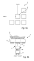
- FIGS. 5 a - b schematically illustrate a sensing element comprised in a sensing system according to a second embodiment of the present invention
- FIG. 6 is a schematic circuit diagram of a part of the sensing element in FIG. 5 b , including the sensing circuitry and the demodulation circuitry;
- FIG. 7 is a timing diagram illustrating an exemplary measurement sequence for the capacitive fingerprint sensing system in FIG. 6 ;
- FIG. 8 schematically illustrates exemplary timing circuitry for controlling the timing of the measurement sequence performed by the sensing element in FIG. 6 ;
- FIG. 9 is a circuit diagram of a delay element comprised in the timing circuitry in FIG. 8 ;
- FIGS. 10 a - b schematically illustrate a third embodiment of the fingerprint sensing system according to the present invention.
- FIG. 11 schematically illustrates embodiments where the excitation signal providing circuitry is arranged and configured to swing a reference potential of the fingerprint sensor component.
- each sensing element comprises excitation signal providing circuitry for providing an excitation or drive signal to the sensing structure.
- the capacitive fingerprint sensing device is illustrated as a touch sensor dimensioned and configured to acquire a fingerprint representation from a stationary finger.
- a capacitive fingerprint sensing system in which the change in potential difference between finger potential and sensing structure potential is instead achieved by controlling the reference potential, such as the local ground level, of the fingerprint sensor component in relation to a reference potential of the electronic system in which the fingerprint sensing system is included.
- Other sensor array configurations such as a so-called swipe sensor (or line sensor) for acquiring a fingerprint representation from a moving finger, are also within the scope of the present invention as defined by the appended claims.
- a touch sensor may also have other dimensions than those illustrated in the appended drawings.
- FIG. 1 schematically illustrates an application for a fingerprint sensing system according to an example embodiment of the present invention, in the form of a mobile phone 1 with an integrated fingerprint sensing system 2 .
- the fingerprint sensing system 2 may, for example, be used for unlocking the mobile phone 1 and/or for authorizing transactions carried out using the mobile phone, etc.
- FIG. 2 schematically shows the fingerprint sensing system 2 comprised in the mobile phone 1 in FIG. 1 .
- the fingerprint sensing system 2 comprises a sensor array 5 , a power supply interface 6 and a communication interface 7 .
- the sensor array 5 comprises a large number of sensing elements 8 (only one of the sensing elements has been indicated with a reference numeral to avoid cluttering the drawing), each being controllable to sense a distance between a sensing structure (top plate) comprised in the sensing element 8 and the surface of a finger contacting the top surface of the sensor array 5 .
- the power supply interface 6 comprises first 10 a and second 10 b contact pads, here shown as bond pads, for connection of a supply voltage V supply to the fingerprint sensor 2 .
- the communication interface 7 comprises a number of bond pads for allowing control of the fingerprint sensor 2 and for acquisition of fingerprint data from the fingerprint sensor 2 .
- FIG. 3 is a schematic cross section of a portion of a fingerprint sensing system according to the prior art, taken along the line A-A′ as indicated in FIG. 2 with a finger 11 placed on top of the sensor array 5 .
- the fingerprint sensing system comprises a plurality of sensing elements 8 , each comprising a protective dielectric top layer 13 , a conductive sensing structure, here in the form of a metal plate 17 underneath the protective dielectric top layer 13 , a charge amplifier 18 , selection circuitry, here functionally illustrated as a simple selection switch 21 for allowing selection/activation of the sensing element 8 , and excitation signal providing circuitry 19 for providing an excitation signal to the finger as is schematically indicated in FIG. 3 .
- the charge amplifier 18 comprises at least one amplifier stage, here schematically illustrated as an operational amplifier (op amp) 24 having a first input (negative input) 25 connected to the sensing structure 17 , a second input (positive input) 26 connected to the excitation signal providing circuitry 19 , and an output 27 .
- the charge amplifier 18 comprises a feedback capacitor 29 connected between the first input 25 and the output 27 , and reset circuitry, here functionally illustrated as a switch 30 , for allowing controllable discharge of the feedback capacitor 29 .
- the charge amplifier 18 may be reset by operating the reset circuitry 30 to discharge the feedback capacitor 29 .
- the voltage at the first input 25 follows the voltage applied to the second input 26 .
- the potential at the first input 25 may be substantially the same as the potential at the second input 26 , or there may be a substantially fixed offset between the potential at the first input 25 and the potential at the second input 26 .
- the provision of the time-varying potential to the finger 11 results in a time-varying potential difference between the sensing structure 17 and the finger 11 .
- the readout line 33 which may be a common readout line for a row or a column of the sensor array 5 in FIG. 2 , is shown in FIG. 3 to be connected to readout circuitry 310 , e.g., a multiplexer 36 . As is schematically indicated in FIG. 3 , additional readout lines providing sensing signals from other rows/columns of the sensor array 5 are also connected to the multiplexer 36 .
- the sensing signals V s from the sensing elements 8 are demodulated by sample-and-hold circuitry 37 arranged outside the array of sensing elements.
- the output of the sample-and-hold circuitry 37 is connected to an analog-to-digital converter 38 for converting the analog DC voltage signals output by the sample-and-hold circuitry to a digital representation of the fingerprint pattern of the finger 11 .
- the readout line 33 there is a parasitic capacitance C p between the readout line 33 and ground.
- a certain current is required for driving the readout line 33 up and down in potential against the parasitic capacitance C p .
- This current is frequency dependent.
- the readout frequency used in known capacitive fingerprint sensing devices such as in the order of 1 MHz
- the power consumption due to the parasitic capacitance of the readout line can be seen as acceptable given that the sensing device is well-designed so that the parasitic capacitance is in the order of, say, 1 pF. If, however, the readout frequency would be considerably increased, to, say, 20 MHz or more, the power consumption due to the parasitic capacitance C p would become substantial.
- Various embodiments of the present invention allow for an increase in readout frequency without the above-described increase in current consumption due to the parasitic capacitance of the readout lines 33 .
- FIGS. 4 a - b A first embodiment of a fingerprint sensing system according to the present invention will now be described with reference to FIGS. 4 a - b.
- the fingerprint sensing system in FIG. 4 a mainly differs from that described above with reference to FIG. 3 in that the excitation signal providing circuitry 19 is coupled to the sensing structure 17 , and in that each sensing element (sensing elements 8 - 1 , 8 - 2 , and 8 - 3 , referred to herein collectively and individually as “sensing element(s) 8 ”) further comprises demodulation circuitry, here in the form of demodulator 31 , and demodulation signal providing circuitry 32 .
- the demodulation circuitry may comprise signal multiplication circuitry 320 for multiplying the sensing signal with the demodulation signal.
- the demodulation circuitry may further comprise a low-pass filter 325 for allowing the DC signal component to pass while removing higher frequency components.
- the finger 11 is schematically indicated as being “grounded” in FIG. 4 a .
- the finger “ground” may be different from the sensor ground.
- the finger may be at the ground potential of the electronic device in which the capacitive fingerprint sensing system is included.
- the body may be considered to have such a large electrical “mass” that the potential of the finger remains substantially constant when the potential of the reference structure 17 varies.
- the demodulation signal providing circuitry 32 is connected to the excitation signal providing circuitry 19 for providing a demodulation signal 322 based on the excitation signal output by the excitation signal providing circuitry.
- the demodulation signal 322 is timing-related to the excitation signal, and is thus also timing-related to the sensing signal Vs output by the charge amplifier 18 .
- the demodulator 31 is connected to the output 27 of the charge amplifier 18 and to the demodulation signal providing circuitry 32 for combining the sensing signal with the demodulation signal 322 to provide a combined signal including a DC signal component indicating the above-mentioned change of charge carried by the sensing structure 17 , resulting from repeated changes in the potential difference between the potential of the finger 11 and the potential of the sensing structure 17 .
- the demodulation signal providing circuitry 32 may generate one or several demodulation signal(s) 322 having a timing relation to the excitation signal.
- An example of demodulation signal providing circuitry 32 in the form of timing circuitry generating sampling control signals for a demodulator in the form of a double sampler will be described further below with reference to FIGS. 5 a - b , FIG. 6 , FIG. 7 and FIG. 8 .
- the demodulator 31 may be implemented in various ways known to the skilled person.
- any suitable mixer or demodulator developed for AM-demodulation may be adapted for use in the sensing element in fingerprint sensing systems according to the present invention.
- FIG. 4 b is a circuit diagram of simple demodulating circuitry (mixer) 31 having a first input 35 for receiving the sensing signal V s , a second input 37 for receiving the excitation signal from the excitation signal providing circuitry 19 , and an output 38 for providing a combined signal including a DC signal component indicating the change of charge carried by the sensing structure 17 , which in turn indicates the (electrical) distance between sensing structure 17 and finger 11 .
- mixer simple demodulating circuitry
- FIGS. 5 a - b schematically illustrate a sensing element 8 comprised in a capacitive fingerprint sensing system 2 according to a second embodiment of the present invention.
- a sensing element 8 from the sensor array 5 in FIG. 2 is shown together with its closest neighbors.
- the sensing element(s) 8 to be sensing the capacitive coupling between its sensing structure 17 and the finger 11 may be selected using activation signals from row selection circuitry and column selection circuitry. Such activation signals are indicated as R-ACT and C-ACT in FIG. 5 a.
- each sensing element 8 in the capacitive fingerprint sensing system 2 comprises sensing circuitry 50 (such as the charge amplifier 18 , excitation signal providing circuitry 19 , and demodulator 31 in FIG. 4 ) and timing circuitry 51 .
- the sensing circuitry 50 is connected to the sensing structure (plate) 17 for measuring the change of the charge carried by the sensing structure 17 resulting from a change in a potential difference between the finger 11 and the sensing structure 17 . This measurement is carried out by performing a measurement sequence comprising transitioning through a sequence of measurement states. An example measurement sequence will be described in detail further below with reference to FIG. 6 and FIG. 7 .
- the sensing circuitry 50 has an output for providing the above-mentioned combined signal provided by the demodulator to the readout line 33 .
- the timing circuitry 51 is connected to the sensing circuitry 50 for controlling a timing of at least one of the measurement states.
- the timing circuitry 51 may receive one or several control signals for triggering a measurement operation of the sensing element 8 .
- the above-mentioned row and column activation signals R-ACT and C-ACT may be received by the timing circuitry 51 , which thereafter may independently provide to the sensing circuitry 50 various timing control signals as is schematically indicated by the arrows in FIG. 5 b.
- the timing of transitions between measurement states can be more precisely and/or uniformly controlled, which allows for shorter times between transitions, which in turn allows for a higher measurement frequency.
- FIG. 6 An example of the sensing circuitry 50 in FIG. 5 b is shown in greater detail in FIG. 6 .
- Control signals provided by the timing circuitry 51 are indicated by arrows in FIG. 6 .
- the sensing circuitry 50 in FIG. 6 comprises a charge amplifier 18 , excitation signal providing circuitry here represented by a controllable voltage source 19 , and a demodulator in the form of sample-and-hold circuitry 74 .
- the charge amplifier in the sensing circuitry 50 of FIG. 6 comprises a negative input 25 , a positive input 26 , an output 27 , a feedback capacitor 29 , and an amplifier 24 .
- the negative input 25 is connected to the sensing structure (plate) 17 and the output 27 is connected to sample-and-hold circuitry 74 comprised in the sensing element 8 .
- the feedback capacitor 29 is connected between the negative input 25 and the output 27 and defines the amplification of the charge amplifier 18 , and the sensing element 8 further comprises a reset switch 30 in parallel with the feedback capacitor 29 .
- the positive input 26 is connected to the controllable voltage source 19 .
- the sample-and-hold circuitry 74 comprises a first sampling capacitor 75 , a first sampling switch 76 and a first output 77 , and a second sampling capacitor 79 , a second sampling switch 80 and a second output 81 .
- a difference amplifier 82 has a positive input connected to the first output 77 and a negative input connected to the second output 81 of the sample-and-hold circuitry 74 .
- the output of the difference amplifier 82 is connected to readout line 33 .
- FIG. 7 illustrates an exemplary measurement sequence for the sensing element 8 in FIG. 6 .
- the measurement sequence illustrated in FIG. 7 can be performed considerably faster, enabling faster readout and/or multiple readings from each sensing elements resulting in improved measurement performance.
- the timing diagram shown therein comprises, from top to bottom, an activation signal ACT, a drive (excitation) control signal DRV, a reset signal RST, a first sampling control signal S 1 , and a second sampling control signal S 2 .
- a row-selection signal and a column selection signal indicating the sensing element 8 may typically be provided.
- selection signals are represented by a single activation signal ACT.
- the sensing element 8 is activated by a transition of the activation signal ACT from low to high. This may, for example, involve activating the amplifier 24 .
- the drive (excitation) control signal DRV provided by the timing circuitry 51 to the excitation signal providing circuitry 19 is controlled to go from low to high.
- a reset signal RST is provided at the time t 2 to close the reset switch 30 to thereby discharge the feedback capacitor and reference the potential at the output 27 of the charge amplifier 18 to the potential of the sensing structure (plate) 17 .
- the reset switch 30 is released (allowed to open again) at the time t 3 , to thereby transition to the third measurement state S 3 (measurement ready state).
- the drive signal DRV goes from high to low to change the potential difference between the finger 11 and the sensing structure 17 .
- This is also the transition to the sixth measurement state S 6 as is schematically indicated in FIG. 7 .
- the ninth measurement state S 9 is identical to the initial “inactive” state S 0 .
- the sensing circuitry 50 can be controlled to perform the measurement sequence described above with reference to FIG. 7 using the above-mentioned control signals (the activation signal ACT, the reset signal RST, the drive control signal DRV, the first sampling control signal S 1 and the second sampling control signal S 2 ).
- the potential difference between the first 77 and second 81 outputs of the sample-and-hold circuit 74 will be indicative of the capacitive coupling between the sensing structure 17 and the finger 11 .
- This potential difference is provided to the output line 33 via difference amplifier 82 .
- the demodulation circuitry is formed by the sample-and-hold circuit 74 , and the DC signal component indicating the change in charge is provided by combining the sensing signal at the output 27 of the charge amplifier 18 with the sampling control signals S 1 and S 2 .
- the sampling control signals are timing-related to the excitation signal, and are generated by demodulation signal providing circuitry in the form of the timing circuit 51 .
- circuit diagram in FIG. 6 has been simplified to facilitate description of embodiments of the present invention. For instance, level shifting at the output of the sensing element 8 has been omitted. Implementation of level shifting is, however, straight-forward to one of ordinary skill in the art. Furthermore, a simple example of a level shifter will be described further below with reference to FIG. 10 a.
- the timing circuit 51 comprises a first AND-gate 83 , a first delay element 84 , a second delay element 85 , a second AND-gate 86 , a first inverter 87 , a third delay element 88 , a fourth delay element 89 , a third AND-gate 90 , a second inverter 91 , a fifth delay element 92 , a sixth delay element 93 , a fourth AND-gate 94 , a third inverter 95 , a seventh delay element 96 , an eighth delay element 97 , a fifth AND-gate 98 , and a fourth inverter 99 .
- the row activation signal R-ACT and the column activation signal C-ACT are input to the first logic AND-gate 83 .
- the output of the first AND-gate 83 is provided to the amplifier 24 of the sensing circuitry 50 as the above-mentioned activation signal ACT, to the input of the first delay element 84 , and to the fourth AND-gate 94 .
- the output of the first delay element 84 is provided to the second AND-gate 86 , and to the input of the second delay element 85 .
- the output of the second delay element 85 is provided to the second AND-gate 86 via the first inverter 87 and to the input of the third delay element 88 .
- the output of the third delay element 88 is provided to the input of the third AND-gate 90 and to the input of the fourth delay element 89 .
- the output of the fourth delay element 89 is provided to the third AND-gate 90 via the second inverter 91 , and to the input of the fifth delay element 92 .
- the output of the fifth delay element 92 is provided to the input of the sixth delay element 93 .
- the output of the sixth delay element 93 is provided to the fourth AND-gate 94 via the third inverter 95 , and to the input of the seventh delay element 96 .
- the output of the seventh delay element 96 is provided to the input of the eighth delay element 97 and the input of the fifth AND-gate 98 .
- the output of the eighth delay element 97 is provided to the input of the fifth AND-gate 98 via the fourth inverter 99 .
- the sensing element 8 comprising the sensing circuitry 50 in FIG. 6 and the timing circuit 51 in FIG. 8 is selected by setting both the row activation signal R-ACT and the column activation signal C-ACT high
- the activation signal ACT for the sensing element 8 goes high (at the time t 1 with reference to FIG. 7 ).
- the output from the first AND-gate 83 passes through the first delay element 84 and is delayed by a first time delay ⁇ T 1 to provide a first delayed version of the activation signal ACT to the second AND-gate 86 .
- the first time delay ⁇ T 1 corresponds to t 2 -t 1 in FIG. 7 and determines the duration of the first measurement state S 1 .
- the output from the first delay element 84 is also provided to the input of the second delay element 85 , and is delayed to provide a second delayed version of the activation signal ACT.
- the second delayed version of the activation signal ACT is provided to the input of the second AND-gate 86 via the first inverter 87 to achieve the reset control signal RST on the output of the second AND-gate 86 .
- the second time delay ⁇ T 2 corresponds to t 3 -t 2 in FIG. 7 and determines the duration of the second measurement state S 2 (where the reset control signal RST is high).
- the remainder of the timing circuit 51 works in the same way, with the delay elements being configured to achieve the control signals shown in the timing diagrams of FIG. 7 .
- the third time delay ⁇ T 3 corresponds to t 4 -t 3 in FIG. 7 and determines the duration of the third measurement state S 3
- the fourth time delay ⁇ T 4 corresponds to t 5 -t 4 in FIG. 7 and determines the duration of the fourth measurement state S 4 etc.
- timing circuit 51 is a simplified example for illustrating the principle of using a combination of delay elements and logic gates for locally controlling the timing of measurement states of the charge measuring circuitry comprised in the sensing element.
- the timing circuitry may comprise additional or other circuitry for, for instance, signal shaping and/or timing. Based on the description provided herein, the skilled person will be able to design a suitable implementation of a timing circuit without undue burden.
- timing control signals may be independently provided from the timing circuitry 51 to the sensing circuitry 50 depending on the particular embodiment.
- FIG. 9 shows an illustrative example of a delay element 100 which may be comprised in the timing circuitry 51 in FIG. 8 .
- the delay element 101 comprises a first CMOS-inverter 101 and a second CMOS-inverter 102 connected in series.
- the time delay of this delay element will depend on the dimensioning of the components comprised in the delay element 100 , and the time delay can thus be set when designing the delay element. If considerably longer delay times are desired, further CMOS-inverters can be coupled in series.
- FIGS. 10 a - b A third embodiment of the fingerprint sensing system 2 in FIG. 2 will now be described with reference to FIGS. 10 a - b .
- the embodiment of FIGS. 10 a - b provides for removal or at least a considerable reduction of the influence of parasitic capacitances in the sensing element 8 , which in turn further facilitates high frequency operation of the sensing element 8 .
- FIG. 10 a is a hybrid of a partly structural and partly circuit schematic illustration of an embodiment of the sensing element 8 in FIG. 2 formed on a doped semiconductor substrate 110 .
- the protective dielectric layer 13 , the sensing plate 17 , a shielding plate 65 and a reference plate 66 are schematically shown in an exploded perspective view, while the charge amplifier 18 is illustrated in the form of a transistor level circuit schematic.
- this example of a simple charge amplifier 18 comprises sense transistor 68 , cascode transistor 69 , reset circuitry in the form of reset transistor 30 and bias current source 71 .
- the sense transistor 68 , the cascode transistor 69 and the reset transistor 30 are all formed in the same well 73 (n-well, p-well or iso-well).
- an interface 115 between the well 73 and the substrate 110 can be configured in such a way that current can be prevented from flowing between the well and the substrate.
- FIG. 10 b the same schematic configuration is also shown in FIG. 10 b , on a more abstract level with the transistor circuitry of FIG. 10 a replaced by a general symbol for a charge amplifier having its negative input 25 connected to the sensing plate 17 , its positive input 26 connected to excitation signal providing circuitry 19 , here in the form of a pulse generator, and its output 27 providing a sensing signal V s indicative of the change in charge carried by the sensing plate 17 resulting from a change in a potential difference between the finger 11 and the sensing plate 17 .
- the change in potential difference between the finger 11 and the sensing plate 17 results from the changing electric potential applied to the sensing plate 17 by the pulse generator 19 via the charge amplifier.
- a feedback capacitor formed by the sensing plate 17 and the reference plate 66 , is connected between the negative input 25 and the output 27 of the charge amplifier. It should be noted that the general functionality of a charge amplifier is well known to one of ordinary skill in the relevant art. FIG. 10 b also schematically indicates that the well 73 is connected to the excitation signal providing circuitry 19 .
- the gate of the sense transistor 68 constitutes the negative input 25 of the charge amplifier and that the source of the sense transistor 68 constitutes the positive input 26 of the charge amplifier.
- the positive input 26 of the charge amplifier is connected to the shielding plate 65 , which is in turn connected to the well 73 in which the sense transistor 68 is formed, and to the pulse generator 19 .
- the sensing element 8 further comprises a drive transistor 75 , a drive control switch 76 and a reset control switch 77 .
- the drive control switch 76 is controllable between a first state in which the gate of the drive transistor 75 is connected to the pulse generator 19 and a second state in which the gate of the drive transistor 75 is connected to sensor ground.
- the drive control switch 76 When the drive control switch 76 is in its first state, the drive transistor 75 will be conducting and thus connect the sensing structure 17 directly to the pulse generator 19 .
- the drive control switch is in its second state, the drive transistor 75 will be non-conducting. In the latter case, there will thus be no direct connection through the drive transistor 75 between the sensing structure 17 and the pulse generator 19 .
- the drive transistor 75 is formed in the well 73 .
- the bias current source 71 can be in the sensing element or outside the sensor array 5 .
- the reset control switch 77 is controllable between a first state in which the reset transistor 30 is non-conducting to allow a potential difference between the sensing plate 17 and the feedback plate 66 , and a second state in which the reset transistor 30 is conducting to equalize the potentials of the sensing plate 17 and the feedback plate 66 .
- the sensing element 8 further comprises a simple level shifter and demodulation circuitry 31 in the form of a sampler like the one described above with reference to FIG. 6 .
- the level shifter comprises a transistor 105 , a first resistor 106 and a second resistor 107 , and works by first converting the sensing signal at the output 27 of the charge amplifier to a current, and then convert the current back to a voltage, which is now referenced to sensor ground.
- the influence of the internal parasitic capacitances C p1 and C p3 is removed or at least considerably reduced. Furthermore, driving neighboring sensing structures will remove or at least considerably reduce the influence of the parasitic capacitance between neighboring sensing plates.
- the excitation signal providing circuitry 19 has been illustrated as being comprised in the fingerprint sensing component.
- the excitation signal providing circuitry 19 comprised in the fingerprint sensing system may alternatively be provided outside the fingerprint sensor component and be arranged and configured to swing a reference potential of the fingerprint sensor component (sensor ground) between the above-mentioned first and second potentials, in relation to the potential of the finger 11 .
- FIG. 11 schematically shows a fingerprint sensing system 2 comprising a fingerprint sensor 4 , processing circuitry 125 , here in the form of a microprocessor, and power supply circuitry 126 .
- the fingerprint sensor 4 comprises, as was also described above with reference to FIG. 2 , a sensor array 5 , a power supply interface 6 and a communication interface 7 .
- the communication interface 7 may, for example, be provided in the form of an SPI-interface (Serial Peripheral Interface).
- the microprocessor 125 acquires fingerprint data from the fingerprint sensor 4 and may process the fingerprint data as required by the application. For instance, the microprocessor 125 may run a fingerprint matching (verification and/or identification) algorithm.
- the power supply circuitry 126 comprises a sensor voltage source 127 configured to output the supply voltage V supply and excitation signal providing circuitry, here a square wave pulse generator 19 , for modulating the low potential side of the sensor voltage source 127 in relation to a reference potential DGND of the electronic device 1 in which the fingerprint sensing system 2 is included.
- a sensor voltage source 127 configured to output the supply voltage V supply and excitation signal providing circuitry, here a square wave pulse generator 19 , for modulating the low potential side of the sensor voltage source 127 in relation to a reference potential DGND of the electronic device 1 in which the fingerprint sensing system 2 is included.
- the pulse generator may generate any other suitable pulse shape, such as a sine wave or a saw tooth signal etc.
- the sensor voltage source 127 may be provided in the form of a constant voltage source, such as a battery, dedicated to supplying power to the fingerprint sensor 4 .
- the sensor voltage source 127 may comprise isolation circuitry for at least partly isolating a voltage source from the fingerprint sensor 4 .
- the fingerprint sensing system 2 may optionally additionally include isolation circuitry 129 for providing galvanic isolation or level shifting between the sensor array 5 and the microprocessor 125 .
- isolation circuitry 129 the microprocessor 125 is allowed to work independently of the varying, in relation to device ground (DGND), reference potential V L of the sensor array 5 .
- the isolation circuitry 129 can be implemented in many different ways known to the skilled person.
- the isolation circuitry 129 may be implemented using components such as opto-couplers, coils and/or capacitors. Although shown here as separate circuitry, it should be understood that the isolation circuitry 129 may be integrated with the fingerprint sensor 4 or the microprocessor 125 .
Abstract
Description
Claims (15)
Applications Claiming Priority (2)
| Application Number | Priority Date | Filing Date | Title |
|---|---|---|---|
| SE1451634-8 | 2014-12-22 | ||
| SE1451634 | 2014-12-22 |
Publications (2)
| Publication Number | Publication Date |
|---|---|
| US20160180619A1 US20160180619A1 (en) | 2016-06-23 |
| US9460576B2 true US9460576B2 (en) | 2016-10-04 |
Family
ID=56130066
Family Applications (1)
| Application Number | Title | Priority Date | Filing Date |
|---|---|---|---|
| US14/812,480 Active US9460576B2 (en) | 2014-12-22 | 2015-07-29 | Capacitive fingerprint sensing device with demodulation circuitry in sensing element |
Country Status (8)
| Country | Link |
|---|---|
| US (1) | US9460576B2 (en) |
| EP (1) | EP3236849A4 (en) |
| JP (1) | JP6651522B2 (en) |
| KR (1) | KR101872368B1 (en) |
| CN (1) | CN106028931B (en) |
| DE (1) | DE112015005726T5 (en) |
| TW (1) | TWI576768B (en) |
| WO (1) | WO2016105263A1 (en) |
Cited By (3)
| Publication number | Priority date | Publication date | Assignee | Title |
|---|---|---|---|---|
| US9864895B1 (en) * | 2016-07-07 | 2018-01-09 | Fingerprint Cards Ab | Fingerprint sensing system with finger detect |
| US10929634B2 (en) | 2016-12-28 | 2021-02-23 | Samsung Display Co., Ltd. | Touch sensor, display device including the same, and operating method of the touch sensor |
| US11783320B2 (en) | 2009-07-02 | 2023-10-10 | Biometric Payment Solutions, Llc | Electronic transaction verification system with biometric authentication |
Families Citing this family (26)
| Publication number | Priority date | Publication date | Assignee | Title |
|---|---|---|---|---|
| US9600705B2 (en) * | 2015-02-11 | 2017-03-21 | Fingerprint Cards Ab | Capacitive fingerprint sensing device with current readout from sensing elements |
| TWM520166U (en) * | 2015-04-27 | 2016-04-11 | 瑞鼎科技股份有限公司 | Capacitive fingerprint sensing apparatus |
| SE539638C2 (en) * | 2016-04-22 | 2017-10-24 | Fingerprint Cards Ab | Fingerprint sensing system with adaptive power control |
| SE1650548A1 (en) * | 2016-04-22 | 2017-10-23 | Fingerprint Cards Ab | Fingerprint sensing system with sensing reference potential providing circuitry |
| JP6975808B2 (en) * | 2016-07-11 | 2021-12-01 | 株式会社ジャパンディスプレイ | Detection device and display device |
| JP6651420B2 (en) | 2016-07-11 | 2020-02-19 | 株式会社ジャパンディスプレイ | Cover member and display device |
| KR20180015025A (en) * | 2016-08-02 | 2018-02-12 | 삼성전자주식회사 | Analog front end for read-out signals from on-display fingerprint sensor and device having the same |
| CN106446780B (en) * | 2016-08-29 | 2018-09-11 | 比亚迪股份有限公司 | Fingerprint sensor and terminal device |
| WO2018041077A1 (en) * | 2016-08-29 | 2018-03-08 | 比亚迪股份有限公司 | Fingerprint sensor and terminal device |
| US10578575B2 (en) * | 2016-09-14 | 2020-03-03 | Sunasic Technologies, Inc. | Noise-reduced capacitive sensing unit |
| CN107918749A (en) * | 2016-10-08 | 2018-04-17 | 深圳指瑞威科技有限公司 | The fingerprint sensor of high-penetration ability based on BCD techniques |
| CN108021843A (en) * | 2016-10-31 | 2018-05-11 | 深圳指瑞威科技有限公司 | High sensitivity fingerprint sensor based on BCD techniques |
| US9922231B1 (en) * | 2016-11-17 | 2018-03-20 | Fingerprint Cards Ab | Fingerprint sensing with voltage pattern configurations |
| US10078776B2 (en) * | 2016-12-16 | 2018-09-18 | Sunasic Technologies Inc. | Noise reduced capacitive fingerprint sensor and capacitive sensing unit included therein |
| CN106709446B (en) * | 2016-12-20 | 2024-03-19 | 深圳芯启航科技有限公司 | Fingerprint identification circuit and device |
| US10002280B1 (en) | 2016-12-21 | 2018-06-19 | Fingerprint Cards Ab | System and method for controlling a signal in a fingerprint sensing device |
| US10346665B2 (en) * | 2017-05-30 | 2019-07-09 | Sunasic Technologies Limited | Noise reduced capacitive image sensor and method operating the same |
| KR101875369B1 (en) * | 2017-07-24 | 2018-07-06 | 주식회사 센소니아 | Fingerprint recognition sensor capable for improving performance with accumulating measuring voltage |
| US10146986B1 (en) * | 2017-07-28 | 2018-12-04 | Sunasic Technologies, Inc. | Capacitive image sensor and method for operating the same |
| CN111433781B (en) * | 2017-12-11 | 2023-11-14 | 指纹卡安娜卡敦知识产权有限公司 | Fingerprint sensing device |
| KR20200090206A (en) * | 2017-12-28 | 2020-07-28 | 커넥텍 재팬 가부시키가이샤 | Image acquisition device and display device provided with it |
| CN108133194B (en) * | 2017-12-30 | 2022-03-15 | 柳州梓博科技有限公司 | Photosensitive circuit, photosensitive device and electronic equipment |
| CN112183246A (en) * | 2017-12-30 | 2021-01-05 | 深圳信炜科技有限公司 | Sensitization drive circuit, sensitization device and electronic equipment |
| CN108073911B (en) * | 2017-12-30 | 2021-10-15 | 柳州梓博科技有限公司 | Photosensitive device, photosensitive module, display module and electronic equipment |
| US11250233B2 (en) * | 2020-06-09 | 2022-02-15 | Wuhan China Star Optoelectronics Technology Co., Ltd | Fingerprint driving circuit and display panel |
| KR20220163758A (en) | 2021-06-03 | 2022-12-12 | 서울대학교산학협력단 | Read-out circuit for a capacitive sensor |
Citations (5)
| Publication number | Priority date | Publication date | Assignee | Title |
|---|---|---|---|---|
| US5565658A (en) * | 1992-07-13 | 1996-10-15 | Cirque Corporation | Capacitance-based proximity with interference rejection apparatus and methods |
| US7864992B2 (en) | 2004-06-18 | 2011-01-04 | Fingerprint Cards Ab | Fingerprint sensor element |
| US20110210939A1 (en) * | 2010-02-26 | 2011-09-01 | Joseph Kurth Reynolds | Varying demodulation to avoid interference |
| US20120268416A1 (en) * | 2011-04-19 | 2012-10-25 | Oleksandr Pirogov | Capacitive sensing with programmable logic for touch sense arrays |
| US9152841B1 (en) * | 2014-03-24 | 2015-10-06 | Fingerprint Cards Ab | Capacitive fingerprint sensor with improved sensing element |
Family Cites Families (12)
| Publication number | Priority date | Publication date | Assignee | Title |
|---|---|---|---|---|
| US5963679A (en) * | 1996-01-26 | 1999-10-05 | Harris Corporation | Electric field fingerprint sensor apparatus and related methods |
| DE10151021A1 (en) * | 2001-10-16 | 2003-04-30 | Infineon Technologies Ag | Sensor arrangement |
| JP4499447B2 (en) * | 2004-03-01 | 2010-07-07 | 日本電信電話株式会社 | Electronic component equipment |
| JP2006071579A (en) * | 2004-09-06 | 2006-03-16 | Alps Electric Co Ltd | Capacitance-detecting circuit and capacitance-detecting method |
| TW200732544A (en) * | 2006-02-21 | 2007-09-01 | Nanogate Optoelectronic Robot Inc | Wireless fingerprint recognition system for electronic lock and method thereof |
| JP2007330420A (en) * | 2006-06-14 | 2007-12-27 | Nippon Telegr & Teleph Corp <Ntt> | Shape detector |
| US7663380B2 (en) * | 2007-12-06 | 2010-02-16 | Himax Technologies Limited | Capacitive fingerprint sensor and the panel thereof |
| CN101727571B (en) * | 2008-10-24 | 2012-09-19 | 宏碁股份有限公司 | Fingerprint sensing device and fingerprint sensing touch device |
| US8421890B2 (en) * | 2010-01-15 | 2013-04-16 | Picofield Technologies, Inc. | Electronic imager using an impedance sensor grid array and method of making |
| US9195877B2 (en) * | 2011-12-23 | 2015-11-24 | Synaptics Incorporated | Methods and devices for capacitive image sensing |
| CN109407862B (en) * | 2012-04-10 | 2022-03-11 | 傲迪司威生物识别公司 | Biometric sensing |
| CN103714330B (en) * | 2014-01-06 | 2017-12-19 | 苏州迈瑞微电子有限公司 | Capacitive fingerprint sensor |
-
2015
- 2015-07-29 US US14/812,480 patent/US9460576B2/en active Active
- 2015-10-22 TW TW104134653A patent/TWI576768B/en active
- 2015-12-15 EP EP15873738.7A patent/EP3236849A4/en active Pending
- 2015-12-15 CN CN201580008847.7A patent/CN106028931B/en active Active
- 2015-12-15 WO PCT/SE2015/051348 patent/WO2016105263A1/en active Application Filing
- 2015-12-15 DE DE112015005726.9T patent/DE112015005726T5/en active Pending
- 2015-12-15 KR KR1020177014919A patent/KR101872368B1/en active IP Right Grant
- 2015-12-15 JP JP2017529641A patent/JP6651522B2/en active Active
Patent Citations (5)
| Publication number | Priority date | Publication date | Assignee | Title |
|---|---|---|---|---|
| US5565658A (en) * | 1992-07-13 | 1996-10-15 | Cirque Corporation | Capacitance-based proximity with interference rejection apparatus and methods |
| US7864992B2 (en) | 2004-06-18 | 2011-01-04 | Fingerprint Cards Ab | Fingerprint sensor element |
| US20110210939A1 (en) * | 2010-02-26 | 2011-09-01 | Joseph Kurth Reynolds | Varying demodulation to avoid interference |
| US20120268416A1 (en) * | 2011-04-19 | 2012-10-25 | Oleksandr Pirogov | Capacitive sensing with programmable logic for touch sense arrays |
| US9152841B1 (en) * | 2014-03-24 | 2015-10-06 | Fingerprint Cards Ab | Capacitive fingerprint sensor with improved sensing element |
Cited By (3)
| Publication number | Priority date | Publication date | Assignee | Title |
|---|---|---|---|---|
| US11783320B2 (en) | 2009-07-02 | 2023-10-10 | Biometric Payment Solutions, Llc | Electronic transaction verification system with biometric authentication |
| US9864895B1 (en) * | 2016-07-07 | 2018-01-09 | Fingerprint Cards Ab | Fingerprint sensing system with finger detect |
| US10929634B2 (en) | 2016-12-28 | 2021-02-23 | Samsung Display Co., Ltd. | Touch sensor, display device including the same, and operating method of the touch sensor |
Also Published As
| Publication number | Publication date |
|---|---|
| WO2016105263A1 (en) | 2016-06-30 |
| DE112015005726T5 (en) | 2017-09-14 |
| TW201624345A (en) | 2016-07-01 |
| TWI576768B (en) | 2017-04-01 |
| KR20170084134A (en) | 2017-07-19 |
| US20160180619A1 (en) | 2016-06-23 |
| CN106028931A (en) | 2016-10-12 |
| KR101872368B1 (en) | 2018-06-28 |
| EP3236849A4 (en) | 2018-12-12 |
| JP2018507455A (en) | 2018-03-15 |
| CN106028931B (en) | 2018-01-02 |
| JP6651522B2 (en) | 2020-02-19 |
| EP3236849A1 (en) | 2017-11-01 |
Similar Documents
| Publication | Publication Date | Title |
|---|---|---|
| US9460576B2 (en) | Capacitive fingerprint sensing device with demodulation circuitry in sensing element | |
| US9600705B2 (en) | Capacitive fingerprint sensing device with current readout from sensing elements | |
| US9449212B2 (en) | Capacitive fingerprint sensor with sensing elements comprising timing circuitry | |
| JP6750059B2 (en) | Capacitive fingerprint sensor with improved sensing element | |
| KR20180088804A (en) | Analog sampling system and noise suppression method in a capacitive fingerprint sensing device | |
| US9710690B1 (en) | Fingerprint sensing system with adaptive power control |
Legal Events
| Date | Code | Title | Description |
|---|---|---|---|
| AS | Assignment |
Owner name: FINGERPRINT CARDS AB, SWEDEN Free format text: ASSIGNMENT OF ASSIGNORS INTEREST;ASSIGNOR:RIEDIJK, FRANK ROBERT;REEL/FRAME:036210/0129 Effective date: 20150702 |
|
| STCF | Information on status: patent grant |
Free format text: PATENTED CASE |
|
| CC | Certificate of correction | ||
| MAFP | Maintenance fee payment |
Free format text: PAYMENT OF MAINTENANCE FEE, 4TH YR, SMALL ENTITY (ORIGINAL EVENT CODE: M2551); ENTITY STATUS OF PATENT OWNER: SMALL ENTITY Year of fee payment: 4 |
|
| AS | Assignment |
Owner name: FINGERPRINT CARDS ANACATUM IP AB, SWEDEN Free format text: ASSIGNMENT OF ASSIGNORS INTEREST;ASSIGNOR:FINGERPRINT CARDS AB;REEL/FRAME:058218/0181 Effective date: 20210907 |
|
| AS | Assignment |
Owner name: FINGERPRINT CARDS ANACATUM IP AB, SWEDEN Free format text: CORRECTIVE ASSIGNMENT TO CORRECT THE PATENT NUMBER 10945920 WHICH SHOULD HAVE BEEN ENTERED AS 10845920 PREVIOUSLY RECORDED ON REEL 058218 FRAME 0181. ASSIGNOR(S) HEREBY CONFIRMS THE ASSIGNMENT;ASSIGNOR:FINGERPRINT CARDS AB;REEL/FRAME:064053/0400 Effective date: 20210907 |
|
| MAFP | Maintenance fee payment |
Free format text: PAYMENT OF MAINTENANCE FEE, 8TH YR, SMALL ENTITY (ORIGINAL EVENT CODE: M2552); ENTITY STATUS OF PATENT OWNER: SMALL ENTITY Year of fee payment: 8 |