US9455152B2 - Hydrogenation method and hydrogenation apparatus - Google Patents
Hydrogenation method and hydrogenation apparatus Download PDFInfo
- Publication number
- US9455152B2 US9455152B2 US14/235,055 US201214235055A US9455152B2 US 9455152 B2 US9455152 B2 US 9455152B2 US 201214235055 A US201214235055 A US 201214235055A US 9455152 B2 US9455152 B2 US 9455152B2
- Authority
- US
- United States
- Prior art keywords
- electrode
- silicon film
- amorphous silicon
- hydrogenation method
- dielectric
- Prior art date
- Legal status (The legal status is an assumption and is not a legal conclusion. Google has not performed a legal analysis and makes no representation as to the accuracy of the status listed.)
- Active, expires
Links
- 238000005984 hydrogenation reaction Methods 0.000 title claims abstract description 192
- 238000000034 method Methods 0.000 title claims abstract description 67
- 229910021417 amorphous silicon Inorganic materials 0.000 claims abstract description 182
- 239000007789 gas Substances 0.000 claims abstract description 172
- UFHFLCQGNIYNRP-UHFFFAOYSA-N Hydrogen Chemical compound [H][H] UFHFLCQGNIYNRP-UHFFFAOYSA-N 0.000 claims abstract description 74
- -1 silane compound Chemical class 0.000 claims abstract description 42
- 238000009832 plasma treatment Methods 0.000 claims abstract description 31
- 229910000077 silane Inorganic materials 0.000 claims abstract description 12
- 229910052751 metal Inorganic materials 0.000 claims description 59
- 239000002184 metal Substances 0.000 claims description 59
- 239000003989 dielectric material Substances 0.000 claims description 21
- PNEYBMLMFCGWSK-UHFFFAOYSA-N aluminium oxide Inorganic materials [O-2].[O-2].[O-2].[Al+3].[Al+3] PNEYBMLMFCGWSK-UHFFFAOYSA-N 0.000 claims description 14
- 239000012535 impurity Substances 0.000 claims description 12
- 239000011368 organic material Substances 0.000 claims description 11
- 239000011261 inert gas Substances 0.000 claims description 9
- 229910010272 inorganic material Inorganic materials 0.000 claims description 9
- 239000011147 inorganic material Substances 0.000 claims description 9
- 125000006850 spacer group Chemical group 0.000 claims description 9
- XYFCBTPGUUZFHI-UHFFFAOYSA-N Phosphine Chemical compound P XYFCBTPGUUZFHI-UHFFFAOYSA-N 0.000 claims description 8
- 239000011521 glass Substances 0.000 claims description 8
- 229920001721 polyimide Polymers 0.000 claims description 7
- 239000004642 Polyimide Substances 0.000 claims description 6
- 239000011810 insulating material Substances 0.000 claims description 6
- 229930040373 Paraformaldehyde Natural products 0.000 claims description 4
- 229910052586 apatite Inorganic materials 0.000 claims description 4
- RBFQJDQYXXHULB-UHFFFAOYSA-N arsane Chemical compound [AsH3] RBFQJDQYXXHULB-UHFFFAOYSA-N 0.000 claims description 4
- 229920003986 novolac Polymers 0.000 claims description 4
- VSIIXMUUUJUKCM-UHFFFAOYSA-D pentacalcium;fluoride;triphosphate Chemical compound [F-].[Ca+2].[Ca+2].[Ca+2].[Ca+2].[Ca+2].[O-]P([O-])([O-])=O.[O-]P([O-])([O-])=O.[O-]P([O-])([O-])=O VSIIXMUUUJUKCM-UHFFFAOYSA-D 0.000 claims description 4
- 229910000073 phosphorus hydride Inorganic materials 0.000 claims description 4
- 229920006324 polyoxymethylene Polymers 0.000 claims description 4
- 238000010438 heat treatment Methods 0.000 claims description 2
- 239000010408 film Substances 0.000 description 172
- 239000000758 substrate Substances 0.000 description 44
- 230000007547 defect Effects 0.000 description 27
- 239000001257 hydrogen Substances 0.000 description 24
- 229910052739 hydrogen Inorganic materials 0.000 description 24
- 229910052710 silicon Inorganic materials 0.000 description 22
- 239000010703 silicon Substances 0.000 description 22
- XUIMIQQOPSSXEZ-UHFFFAOYSA-N Silicon Chemical compound [Si] XUIMIQQOPSSXEZ-UHFFFAOYSA-N 0.000 description 21
- 238000004435 EPR spectroscopy Methods 0.000 description 13
- 238000000137 annealing Methods 0.000 description 12
- 230000005684 electric field Effects 0.000 description 11
- IJGRMHOSHXDMSA-UHFFFAOYSA-N Atomic nitrogen Chemical compound N#N IJGRMHOSHXDMSA-UHFFFAOYSA-N 0.000 description 9
- YXFVVABEGXRONW-UHFFFAOYSA-N Toluene Chemical compound CC1=CC=CC=C1 YXFVVABEGXRONW-UHFFFAOYSA-N 0.000 description 9
- 230000005672 electromagnetic field Effects 0.000 description 9
- 150000002500 ions Chemical class 0.000 description 9
- 239000001307 helium Substances 0.000 description 8
- 229910052734 helium Inorganic materials 0.000 description 8
- SWQJXJOGLNCZEY-UHFFFAOYSA-N helium atom Chemical compound [He] SWQJXJOGLNCZEY-UHFFFAOYSA-N 0.000 description 8
- 238000005259 measurement Methods 0.000 description 8
- 230000015572 biosynthetic process Effects 0.000 description 7
- 239000012299 nitrogen atmosphere Substances 0.000 description 7
- 238000001069 Raman spectroscopy Methods 0.000 description 6
- VYPSYNLAJGMNEJ-UHFFFAOYSA-N Silicium dioxide Chemical compound O=[Si]=O VYPSYNLAJGMNEJ-UHFFFAOYSA-N 0.000 description 6
- 230000008030 elimination Effects 0.000 description 6
- 238000003379 elimination reaction Methods 0.000 description 6
- 239000004065 semiconductor Substances 0.000 description 6
- 238000003786 synthesis reaction Methods 0.000 description 6
- 230000002159 abnormal effect Effects 0.000 description 5
- 238000006243 chemical reaction Methods 0.000 description 5
- 238000004132 cross linking Methods 0.000 description 5
- 238000002425 crystallisation Methods 0.000 description 5
- 230000008025 crystallization Effects 0.000 description 5
- 238000009826 distribution Methods 0.000 description 5
- 238000005224 laser annealing Methods 0.000 description 5
- 239000010410 layer Substances 0.000 description 5
- TWNQGVIAIRXVLR-UHFFFAOYSA-N oxo(oxoalumanyloxy)alumane Chemical compound O=[Al]O[Al]=O TWNQGVIAIRXVLR-UHFFFAOYSA-N 0.000 description 5
- LCGLNKUTAGEVQW-UHFFFAOYSA-N Dimethyl ether Chemical compound COC LCGLNKUTAGEVQW-UHFFFAOYSA-N 0.000 description 4
- 238000004458 analytical method Methods 0.000 description 4
- ZSWFCLXCOIISFI-UHFFFAOYSA-N cyclopentadiene Chemical compound C1C=CC=C1 ZSWFCLXCOIISFI-UHFFFAOYSA-N 0.000 description 4
- 230000006378 damage Effects 0.000 description 4
- 150000002431 hydrogen Chemical class 0.000 description 4
- 238000005468 ion implantation Methods 0.000 description 4
- 239000000203 mixture Substances 0.000 description 4
- 229920000548 poly(silane) polymer Polymers 0.000 description 4
- 229920000642 polymer Polymers 0.000 description 4
- 239000010453 quartz Substances 0.000 description 4
- 238000001004 secondary ion mass spectrometry Methods 0.000 description 4
- XLYOFNOQVPJJNP-UHFFFAOYSA-N water Substances O XLYOFNOQVPJJNP-UHFFFAOYSA-N 0.000 description 4
- RYGMFSIKBFXOCR-UHFFFAOYSA-N Copper Chemical compound [Cu] RYGMFSIKBFXOCR-UHFFFAOYSA-N 0.000 description 3
- RTZKZFJDLAIYFH-UHFFFAOYSA-N Diethyl ether Chemical compound CCOCC RTZKZFJDLAIYFH-UHFFFAOYSA-N 0.000 description 3
- XKRFYHLGVUSROY-UHFFFAOYSA-N argon Substances [Ar] XKRFYHLGVUSROY-UHFFFAOYSA-N 0.000 description 3
- 239000003054 catalyst Substances 0.000 description 3
- 238000007872 degassing Methods 0.000 description 3
- 229910001873 dinitrogen Inorganic materials 0.000 description 3
- 229910052757 nitrogen Inorganic materials 0.000 description 3
- 239000004033 plastic Substances 0.000 description 3
- 229920003023 plastic Polymers 0.000 description 3
- 229910021420 polycrystalline silicon Inorganic materials 0.000 description 3
- 229920005599 polyhydrosilane Polymers 0.000 description 3
- 229920005591 polysilicon Polymers 0.000 description 3
- 239000004810 polytetrafluoroethylene Substances 0.000 description 3
- 229920001343 polytetrafluoroethylene Polymers 0.000 description 3
- 229920005989 resin Polymers 0.000 description 3
- 239000011347 resin Substances 0.000 description 3
- 230000003685 thermal hair damage Effects 0.000 description 3
- 238000005406 washing Methods 0.000 description 3
- MYMOFIZGZYHOMD-UHFFFAOYSA-N Dioxygen Chemical compound O=O MYMOFIZGZYHOMD-UHFFFAOYSA-N 0.000 description 2
- 241001669573 Galeorhinus galeus Species 0.000 description 2
- PWHULOQIROXLJO-UHFFFAOYSA-N Manganese Chemical compound [Mn] PWHULOQIROXLJO-UHFFFAOYSA-N 0.000 description 2
- 229910052581 Si3N4 Inorganic materials 0.000 description 2
- BLRPTPMANUNPDV-UHFFFAOYSA-N Silane Chemical compound [SiH4] BLRPTPMANUNPDV-UHFFFAOYSA-N 0.000 description 2
- 238000010521 absorption reaction Methods 0.000 description 2
- VSCWAEJMTAWNJL-UHFFFAOYSA-K aluminium trichloride Chemical compound Cl[Al](Cl)Cl VSCWAEJMTAWNJL-UHFFFAOYSA-K 0.000 description 2
- 229910052786 argon Inorganic materials 0.000 description 2
- 125000004429 atom Chemical group 0.000 description 2
- QVGXLLKOCUKJST-UHFFFAOYSA-N atomic oxygen Chemical compound [O] QVGXLLKOCUKJST-UHFFFAOYSA-N 0.000 description 2
- 238000005229 chemical vapour deposition Methods 0.000 description 2
- 238000001816 cooling Methods 0.000 description 2
- 229910021419 crystalline silicon Inorganic materials 0.000 description 2
- 229910001882 dioxygen Inorganic materials 0.000 description 2
- 230000000694 effects Effects 0.000 description 2
- 239000012212 insulator Substances 0.000 description 2
- 238000005342 ion exchange Methods 0.000 description 2
- 229910052748 manganese Inorganic materials 0.000 description 2
- 239000011572 manganese Substances 0.000 description 2
- 238000004519 manufacturing process Methods 0.000 description 2
- 239000003550 marker Substances 0.000 description 2
- 239000000463 material Substances 0.000 description 2
- QSHDDOUJBYECFT-UHFFFAOYSA-N mercury Chemical compound [Hg] QSHDDOUJBYECFT-UHFFFAOYSA-N 0.000 description 2
- 230000007935 neutral effect Effects 0.000 description 2
- 239000012044 organic layer Substances 0.000 description 2
- 239000001301 oxygen Substances 0.000 description 2
- 229910052760 oxygen Inorganic materials 0.000 description 2
- HQVNEWCFYHHQES-UHFFFAOYSA-N silicon nitride Chemical compound N12[Si]34N5[Si]62N3[Si]51N64 HQVNEWCFYHHQES-UHFFFAOYSA-N 0.000 description 2
- 229910052814 silicon oxide Inorganic materials 0.000 description 2
- 239000007787 solid Substances 0.000 description 2
- 239000002904 solvent Substances 0.000 description 2
- 238000003756 stirring Methods 0.000 description 2
- 238000007669 thermal treatment Methods 0.000 description 2
- 229920001342 Bakelite® Polymers 0.000 description 1
- 238000006418 Brown reaction Methods 0.000 description 1
- XDTMQSROBMDMFD-UHFFFAOYSA-N Cyclohexane Chemical compound C1CCCCC1 XDTMQSROBMDMFD-UHFFFAOYSA-N 0.000 description 1
- 239000004698 Polyethylene Substances 0.000 description 1
- BQCADISMDOOEFD-UHFFFAOYSA-N Silver Chemical compound [Ag] BQCADISMDOOEFD-UHFFFAOYSA-N 0.000 description 1
- BZHJMEDXRYGGRV-UHFFFAOYSA-N Vinyl chloride Chemical compound ClC=C BZHJMEDXRYGGRV-UHFFFAOYSA-N 0.000 description 1
- 229910007928 ZrCl2 Inorganic materials 0.000 description 1
- 230000002411 adverse Effects 0.000 description 1
- 239000012298 atmosphere Substances 0.000 description 1
- 239000004637 bakelite Substances 0.000 description 1
- 230000005540 biological transmission Effects 0.000 description 1
- 238000004440 column chromatography Methods 0.000 description 1
- 239000012141 concentrate Substances 0.000 description 1
- 238000011109 contamination Methods 0.000 description 1
- 238000010908 decantation Methods 0.000 description 1
- 238000001035 drying Methods 0.000 description 1
- 239000003480 eluent Substances 0.000 description 1
- 239000003822 epoxy resin Substances 0.000 description 1
- 239000000706 filtrate Substances 0.000 description 1
- 238000001914 filtration Methods 0.000 description 1
- 239000012530 fluid Substances 0.000 description 1
- PCHJSUWPFVWCPO-UHFFFAOYSA-N gold Chemical compound [Au] PCHJSUWPFVWCPO-UHFFFAOYSA-N 0.000 description 1
- 230000000977 initiatory effect Effects 0.000 description 1
- 238000007641 inkjet printing Methods 0.000 description 1
- 230000001678 irradiating effect Effects 0.000 description 1
- 229910052743 krypton Inorganic materials 0.000 description 1
- DNNSSWSSYDEUBZ-UHFFFAOYSA-N krypton atom Chemical compound [Kr] DNNSSWSSYDEUBZ-UHFFFAOYSA-N 0.000 description 1
- 238000013532 laser treatment Methods 0.000 description 1
- WABPQHHGFIMREM-UHFFFAOYSA-N lead(0) Chemical compound [Pb] WABPQHHGFIMREM-UHFFFAOYSA-N 0.000 description 1
- 239000007788 liquid Substances 0.000 description 1
- NIXOIRLDFIPNLJ-UHFFFAOYSA-M magnesium;benzene;bromide Chemical compound [Mg+2].[Br-].C1=CC=[C-]C=C1 NIXOIRLDFIPNLJ-UHFFFAOYSA-M 0.000 description 1
- 239000000155 melt Substances 0.000 description 1
- 239000012528 membrane Substances 0.000 description 1
- 229910044991 metal oxide Inorganic materials 0.000 description 1
- 150000004706 metal oxides Chemical class 0.000 description 1
- 238000002156 mixing Methods 0.000 description 1
- 229910021421 monocrystalline silicon Inorganic materials 0.000 description 1
- 229910052754 neon Inorganic materials 0.000 description 1
- GKAOGPIIYCISHV-UHFFFAOYSA-N neon atom Chemical compound [Ne] GKAOGPIIYCISHV-UHFFFAOYSA-N 0.000 description 1
- 239000002245 particle Substances 0.000 description 1
- 239000005011 phenolic resin Substances 0.000 description 1
- PARWUHTVGZSQPD-UHFFFAOYSA-N phenylsilane Chemical compound [SiH3]C1=CC=CC=C1 PARWUHTVGZSQPD-UHFFFAOYSA-N 0.000 description 1
- 229920000647 polyepoxide Polymers 0.000 description 1
- 229920000573 polyethylene Polymers 0.000 description 1
- 239000009719 polyimide resin Substances 0.000 description 1
- 238000011084 recovery Methods 0.000 description 1
- 239000013557 residual solvent Substances 0.000 description 1
- 238000000926 separation method Methods 0.000 description 1
- 238000007711 solidification Methods 0.000 description 1
- 230000008023 solidification Effects 0.000 description 1
- 238000004528 spin coating Methods 0.000 description 1
- 239000006228 supernatant Substances 0.000 description 1
- 230000002194 synthesizing effect Effects 0.000 description 1
- FKHIFSZMMVMEQY-UHFFFAOYSA-N talc Chemical compound [Mg+2].[O-][Si]([O-])=O FKHIFSZMMVMEQY-UHFFFAOYSA-N 0.000 description 1
- 239000010409 thin film Substances 0.000 description 1
- 238000011282 treatment Methods 0.000 description 1
Images


Classifications
-
- H—ELECTRICITY
- H01—ELECTRIC ELEMENTS
- H01L—SEMICONDUCTOR DEVICES NOT COVERED BY CLASS H10
- H01L21/00—Processes or apparatus adapted for the manufacture or treatment of semiconductor or solid state devices or of parts thereof
- H01L21/02—Manufacture or treatment of semiconductor devices or of parts thereof
- H01L21/04—Manufacture or treatment of semiconductor devices or of parts thereof the devices having at least one potential-jump barrier or surface barrier, e.g. PN junction, depletion layer or carrier concentration layer
- H01L21/18—Manufacture or treatment of semiconductor devices or of parts thereof the devices having at least one potential-jump barrier or surface barrier, e.g. PN junction, depletion layer or carrier concentration layer the devices having semiconductor bodies comprising elements of Group IV of the Periodic System or AIIIBV compounds with or without impurities, e.g. doping materials
- H01L21/30—Treatment of semiconductor bodies using processes or apparatus not provided for in groups H01L21/20 - H01L21/26
- H01L21/3003—Hydrogenation or deuterisation, e.g. using atomic hydrogen from a plasma
-
- H—ELECTRICITY
- H01—ELECTRIC ELEMENTS
- H01J—ELECTRIC DISCHARGE TUBES OR DISCHARGE LAMPS
- H01J37/00—Discharge tubes with provision for introducing objects or material to be exposed to the discharge, e.g. for the purpose of examination or processing thereof
- H01J37/32—Gas-filled discharge tubes
- H01J37/32009—Arrangements for generation of plasma specially adapted for examination or treatment of objects, e.g. plasma sources
- H01J37/32192—Microwave generated discharge
-
- H—ELECTRICITY
- H01—ELECTRIC ELEMENTS
- H01J—ELECTRIC DISCHARGE TUBES OR DISCHARGE LAMPS
- H01J37/00—Discharge tubes with provision for introducing objects or material to be exposed to the discharge, e.g. for the purpose of examination or processing thereof
- H01J37/32—Gas-filled discharge tubes
- H01J37/32009—Arrangements for generation of plasma specially adapted for examination or treatment of objects, e.g. plasma sources
- H01J37/32348—Dielectric barrier discharge
-
- H—ELECTRICITY
- H01—ELECTRIC ELEMENTS
- H01L—SEMICONDUCTOR DEVICES NOT COVERED BY CLASS H10
- H01L21/00—Processes or apparatus adapted for the manufacture or treatment of semiconductor or solid state devices or of parts thereof
- H01L21/02—Manufacture or treatment of semiconductor devices or of parts thereof
- H01L21/02104—Forming layers
- H01L21/02365—Forming inorganic semiconducting materials on a substrate
- H01L21/02518—Deposited layers
- H01L21/02521—Materials
- H01L21/02524—Group 14 semiconducting materials
- H01L21/02532—Silicon, silicon germanium, germanium
-
- H—ELECTRICITY
- H01—ELECTRIC ELEMENTS
- H01L—SEMICONDUCTOR DEVICES NOT COVERED BY CLASS H10
- H01L21/00—Processes or apparatus adapted for the manufacture or treatment of semiconductor or solid state devices or of parts thereof
- H01L21/02—Manufacture or treatment of semiconductor devices or of parts thereof
- H01L21/02104—Forming layers
- H01L21/02365—Forming inorganic semiconducting materials on a substrate
- H01L21/02518—Deposited layers
- H01L21/02587—Structure
- H01L21/0259—Microstructure
- H01L21/02592—Microstructure amorphous
-
- H—ELECTRICITY
- H01—ELECTRIC ELEMENTS
- H01L—SEMICONDUCTOR DEVICES NOT COVERED BY CLASS H10
- H01L21/00—Processes or apparatus adapted for the manufacture or treatment of semiconductor or solid state devices or of parts thereof
- H01L21/02—Manufacture or treatment of semiconductor devices or of parts thereof
- H01L21/02104—Forming layers
- H01L21/02365—Forming inorganic semiconducting materials on a substrate
- H01L21/02612—Formation types
- H01L21/02617—Deposition types
- H01L21/02623—Liquid deposition
- H01L21/02628—Liquid deposition using solutions
-
- H—ELECTRICITY
- H01—ELECTRIC ELEMENTS
- H01L—SEMICONDUCTOR DEVICES NOT COVERED BY CLASS H10
- H01L21/00—Processes or apparatus adapted for the manufacture or treatment of semiconductor or solid state devices or of parts thereof
- H01L21/02—Manufacture or treatment of semiconductor devices or of parts thereof
- H01L21/02104—Forming layers
- H01L21/02365—Forming inorganic semiconducting materials on a substrate
- H01L21/02656—Special treatments
- H01L21/02664—Aftertreatments
-
- H—ELECTRICITY
- H01—ELECTRIC ELEMENTS
- H01L—SEMICONDUCTOR DEVICES NOT COVERED BY CLASS H10
- H01L21/00—Processes or apparatus adapted for the manufacture or treatment of semiconductor or solid state devices or of parts thereof
- H01L21/67—Apparatus specially adapted for handling semiconductor or electric solid state devices during manufacture or treatment thereof; Apparatus specially adapted for handling wafers during manufacture or treatment of semiconductor or electric solid state devices or components ; Apparatus not specifically provided for elsewhere
- H01L21/67005—Apparatus not specifically provided for elsewhere
- H01L21/67011—Apparatus for manufacture or treatment
- H01L21/67017—Apparatus for fluid treatment
-
- H—ELECTRICITY
- H01—ELECTRIC ELEMENTS
- H01L—SEMICONDUCTOR DEVICES NOT COVERED BY CLASS H10
- H01L21/00—Processes or apparatus adapted for the manufacture or treatment of semiconductor or solid state devices or of parts thereof
- H01L21/67—Apparatus specially adapted for handling semiconductor or electric solid state devices during manufacture or treatment thereof; Apparatus specially adapted for handling wafers during manufacture or treatment of semiconductor or electric solid state devices or components ; Apparatus not specifically provided for elsewhere
- H01L21/67005—Apparatus not specifically provided for elsewhere
- H01L21/67011—Apparatus for manufacture or treatment
- H01L21/67098—Apparatus for thermal treatment
- H01L21/67115—Apparatus for thermal treatment mainly by radiation
-
- H—ELECTRICITY
- H01—ELECTRIC ELEMENTS
- H01L—SEMICONDUCTOR DEVICES NOT COVERED BY CLASS H10
- H01L29/00—Semiconductor devices adapted for rectifying, amplifying, oscillating or switching, or capacitors or resistors with at least one potential-jump barrier or surface barrier, e.g. PN junction depletion layer or carrier concentration layer; Details of semiconductor bodies or of electrodes thereof ; Multistep manufacturing processes therefor
- H01L29/02—Semiconductor bodies ; Multistep manufacturing processes therefor
- H01L29/12—Semiconductor bodies ; Multistep manufacturing processes therefor characterised by the materials of which they are formed
- H01L29/16—Semiconductor bodies ; Multistep manufacturing processes therefor characterised by the materials of which they are formed including, apart from doping materials or other impurities, only elements of Group IV of the Periodic System
- H01L29/1604—Amorphous materials
-
- H—ELECTRICITY
- H05—ELECTRIC TECHNIQUES NOT OTHERWISE PROVIDED FOR
- H05H—PLASMA TECHNIQUE; PRODUCTION OF ACCELERATED ELECTRICALLY-CHARGED PARTICLES OR OF NEUTRONS; PRODUCTION OR ACCELERATION OF NEUTRAL MOLECULAR OR ATOMIC BEAMS
- H05H1/00—Generating plasma; Handling plasma
- H05H1/24—Generating plasma
- H05H1/2406—Generating plasma using dielectric barrier discharges, i.e. with a dielectric interposed between the electrodes
-
- H—ELECTRICITY
- H05—ELECTRIC TECHNIQUES NOT OTHERWISE PROVIDED FOR
- H05H—PLASMA TECHNIQUE; PRODUCTION OF ACCELERATED ELECTRICALLY-CHARGED PARTICLES OR OF NEUTRONS; PRODUCTION OR ACCELERATION OF NEUTRAL MOLECULAR OR ATOMIC BEAMS
- H05H1/00—Generating plasma; Handling plasma
- H05H1/24—Generating plasma
- H05H1/46—Generating plasma using applied electromagnetic fields, e.g. high frequency or microwave energy
- H05H1/4645—Radiofrequency discharges
- H05H1/466—Radiofrequency discharges using capacitive coupling means, e.g. electrodes
-
- H—ELECTRICITY
- H05—ELECTRIC TECHNIQUES NOT OTHERWISE PROVIDED FOR
- H05H—PLASMA TECHNIQUE; PRODUCTION OF ACCELERATED ELECTRICALLY-CHARGED PARTICLES OR OF NEUTRONS; PRODUCTION OR ACCELERATION OF NEUTRAL MOLECULAR OR ATOMIC BEAMS
- H05H1/00—Generating plasma; Handling plasma
- H05H1/24—Generating plasma
- H05H1/46—Generating plasma using applied electromagnetic fields, e.g. high frequency or microwave energy
- H05H1/461—Microwave discharges
-
- H05H2001/2412—
-
- H05H2001/4607—
-
- H05H2001/466—
Definitions
- the present invention relates to hydrogenation methods and hydrogenation apparatuses.
- Semiconductor devices including a silicon film have been widely used for electronic devices, such as display devices, controllers, etc.
- monocrystalline silicon has high conductivity.
- an amorphous silicon film or a polysilicon film is usually used as the semiconductor film.
- the amorphous silicon film which has insufficiently conductivity, is subjected to annealing to improve the property in many cases.
- thermal annealing is performed on the amorphous silicon film.
- the amorphous silicon film is exposed to comparatively high temperatures to form the polysilicon film.
- the amorphous silicon film is exposed to temperatures in the range from 600° C. to 1100° C. for several ten hours in the thermal annealing.
- thermal annealing at a temperature of 500° C. or lower hardly provides effects, and therefore, it is difficult to perform the thermal annealing using a comparatively low-cost and excellently-processable substrate, such as a glass substrate and a plastic substrate, as a substrate for supporting the amorphous silicon film.
- laser annealing has been known as another annealing.
- the laser annealing is performed in such a manner that laser light is irradiated to the amorphous silicon film to form the polysilicon film.
- the laser annealing can provide comparatively high energy partially to the amorphous silicon film, so that a substrate that supports the silicon film is not exposed to high temperatures as a whole. Accordingly, a glass substrate and a plastic substrate, which have comparatively low thermal resistance, can be used as the substrate.
- the laser annealing uses a continuous wave laser or a pulsed laser.
- the continuous wave laser such as an argon ion laser
- a light beam having a spot with a diameter of about 100 ⁇ m is irradiated to the silicon film, thereby performing scan by the light beam on the silicon film.
- the silicon film is gradually solidified according to the energy distribution inside the light beam and movement of the light beam to cause crystallization of the silicon film.
- the spot diameter of the light beam is small, it may take long time generally for the use of the continuous wave laser to thoroughly eliminate defects in the silicon film, which is comparatively wide.
- the pulsed laser such as an eximer laser
- the silicon film is instantly melted.
- the silicon film is solidified thereafter, the silicon film is crystallized.
- the spot diameter of the light beam can be increased comparatively large with comparatively high maximum energy of the laser light, the spot diameter of the light beam is still not so large relative to the silicon film. Accordingly, it may take long time to thoroughly eliminate defects of a comparatively large area of the silicon film.
- thermal damage to the substrate may accordingly increase.
- the use of a substrate with a thickness of smaller than 1 mm which has been recently employed in general, may cause thermal damage to deform the substrate.
- Patent Literature 1 Besides the thermal annealing and the laser annealing, hydrogen plasma treatment has been known as a scheme for defect elimination (see Patent Literature 1).
- the hydrogen plasma treatment disclosed in Patent Literature 1 is performed on an amorphous silicon film under low pressures (e.g., 150 mTorr). This may terminate dangling bonds of the amorphous silicon film with hydrogen to eliminate bonding defects.
- hydrogen ions with small atomic weight may have comparatively high kinetic energy to cause physical damage to the amorphous silicon film.
- the present invention has been made in view of the foregoing and has its object of providing a hydrogenation method and a hydrogenation apparatus suitable for defect elimination.
- a hydrogenation method includes: preparing a plasma generation section; preparing a hermetic member; disposing an amorphous silicon film inside the hermetic member; and performing plasma treatment on the amorphous silicon film in a manner that the plasma generation section allows a gas at a pressure around an atmospheric pressure containing a hydrogen gas to generate plasma in at least a partial region inside the hermetic member.
- the disposing an amorphous silicon film includes forming the amorphous silicon film inside the hermetic member with the use of a solution in which a silane compound is dissolved.
- the method further includes disposing the plasma generation section inside the hermetic member.
- the method further includes supplying the gas containing the hydrogen gas to the hermetic member.
- the supplying the gas is performed after the amorphous silicon film is disposed.
- the supplying the gas is performed before the amorphous silicon film is disposed, and the disposing an amorphous silicon film includes forming the amorphous silicon film inside the hermetic member to which the gas containing the hydrogen gas is supplied.
- the disposing an amorphous silicon film includes forming the amorphous silicon film inside the hermetic member with the use of the solution in which the silane compound is dissolved after the gas containing the hydrogen gas is supplied, and in the performing plasma treatment, the plasma is allowed to be generated without changing the gas inside the hermetic member at the time when the amorphous silicon film is formed.
- the method further includes performing temporary baking on the amorphous silicon film.
- the gas in the performing plasma treatment, is a mixed gas containing the hydrogen gas and an inert gas.
- the hydrogen gas in the mixed gas, has a concentration of 0.1 weight % or higher.
- the mixed gas contains a gas containing a p-type impurity element or an n-type impurity element.
- the mixed gas contains any of diborane, phosphine, and arsine.
- the plasma generation section in the preparing a plasma generation section, includes a first electrode and a second electrode.
- one of the first electrode and the second electrode is grounded.
- the amorphous silicon film is disposed between the first electrode and the second electrode.
- the amorphous silicon film is moved so as to pass between the first electrode and the second electrode in generating the plasma.
- the performing plasma treatment includes sliding the amorphous silicon film so as to pass between the first electrode and the second electrode.
- the plasma in the performing plasma treatment, is generated between the first electrode and the second electrode in a state where the gas inside the hermetic member flows so as to pass between the first electrode and the second electrode and reach the amorphous silicon film.
- At least one of the first electrode and the second electrode is a linear electrode including two or more conductive parts extending in stripes, and the conductive parts have a bulk shape or a mesh-like shape.
- a dielectric is mounted at at least one of the first electrode and the second electrode.
- the dielectric is made of an inorganic material or an organic material.
- the inorganic material includes glass, alumina, or apatite.
- the organic material includes polyimide, polyoxymethylene, or novolac resin.
- At least one of the first electrode and the second electrode is a linear electrode including two or more conductive parts extending in stripes.
- the dielectric in the preparing a plasma generation section, is mounted at one of the first electrode and the second electrode.
- the second electrode is grounded.
- the dielectric includes a dielectric plate mounted at the first electrode.
- the first electrode is arranged opposite to the second electrode with the dielectric plate interposed therebetween.
- either the first electrode or the second electrode is disposed 0.5 mm or more apart from the amorphous silicon film.
- the dielectric in the preparing a plasma generation section, includes a first dielectric mounted at the first electrode and a second dielectric mounted at the second electrode.
- the first dielectric includes a first dielectric plate
- the second dielectric includes a second dielectric plate.
- the second electrode is grounded.
- a spacer made of a dielectric material is provided between the first dielectric plate and the second dielectric plate.
- the amorphous silicon film is disposed 0.5 mm or more apart from the first dielectric plate.
- the first electrode includes a rod-shaped electrode surrounded by and covered with the first dielectric.
- the first dielectric is made of an organic insulating material.
- the second electrode includes a metal plate or a metal mesh fixed at the bottom of the second dielectric.
- the second electrode is grounded.
- the amorphous silicon film is disposed between the first electrode and the second electrode.
- the amorphous silicon film is arranged 0.5 mm or more apart from the first electrode.
- the second electrode is grounded.
- the dielectric is mounted at only the first electrode.
- the first electrode is arranged opposite to the second electrode with the dielectric interposed therebetween.
- the first electrode and the second electrode are disposed on the dielectric, and each of the first electrode and the second electrode is covered with an organic material.
- the first electrode is arranged opposite to the second electrode with no dielectric interposed therebetween.
- the performing plasma treatment includes applying alternating voltage between the first electrode and the second electrode.
- the alternating voltage is 25 volts or higher and 100 kilovolts or lower and has a frequency of 60 hertz or higher and 1 megahertz or lower.
- the alternating voltage has a waveform of any of a sine wave, a triangular wave, and a rectangular wave.
- the performing plasma treatment includes heating the amorphous silicon film with a heater.
- the performing plasma treatment includes setting the amorphous silicon film in a range between minus 30° C. and 900° C.
- a crystalline state of the amorphous silicon film is controlled according to an ionized gas density.
- the plasma generation section in the preparing a plasma generation section, includes a coil.
- the plasma generation section in the preparing a plasma generation section, includes a microwave generation section and an antenna.
- a hydrogenation apparatus includes: a plasma generation section; and a hermetic member, wherein the plasma generation section allows a gas at a pressure around an atmospheric pressure containing a hydrogen gas to generate plasma in at least a partial region inside the hermetic member.
- the plasma generation section includes a first electrode and a second electrode.
- the plasma generation section includes a coil.
- the plasma generation section includes a microwave generation section and an antenna.
- a hydrogenation method and a hydrogenation apparatus can be provided which are suitable for elimination of bonding defects.
- FIG. 1 is a schematic illustration of one embodiment of a hydrogenation apparatus according to the present invention.
- FIGS. 2A-2D are schematic illustrations for explaining one embodiment of a hydrogenation method according to the present invention.
- FIGS. 3A-3C are schematic illustrations each showing a hydrogenation apparatus according to one embodiment.
- FIG. 4 is a schematic illustration of a hydrogenation apparatus according to one embodiment.
- FIGS. 5A and 5B are schematic illustrations for explaining one embodiment of a hydrogenation method according to the present invention.
- FIG. 6 is a schematic illustration of one embodiment of a hydrogenation apparatus according to the present invention.
- FIG. 7A is a schematic illustration showing a hydrogenation apparatus according to one embodiment.
- FIG. 7B is a schematic illustration of a discharge electrode of the hydrogenation apparatus shown in FIG. 7A as viewed from above.
- FIG. 7C is a schematic illustration of a ground electrode of the hydrogenation apparatus shown in FIG. 7A as viewed from below.
- FIG. 8A is a schematic illustration of a hydrogenation apparatus according to one embodiment.
- FIG. 8B is a schematic illustration of a discharge electrode of the hydrogenation apparatus shown in FIG. 8A as viewed from above.
- FIG. 8C is a schematic illustration of a ground electrode of the hydrogenation apparatus shown in FIG. 8A as viewed from below.
- FIG. 9A is a schematic illustration showing a hydrogenation apparatus according to one embodiment.
- FIG. 9B is a schematic illustration of a discharge electrode of the hydrogenation apparatus shown in FIG. 9A as viewed from above.
- FIG. 9C is a schematic illustration of a ground electrode of the hydrogenation apparatus shown in FIG. 9A as viewed from below.
- FIG. 10A is a schematic illustration showing a hydrogenation apparatus according to one embodiment.
- FIG. 10B is a schematic illustration of a discharge electrode of the hydrogenation apparatus shown in FIG. 10A as viewed from above.
- FIG. 10C is a schematic illustration of a ground electrode of the hydrogenation apparatus shown in FIG. 10A as viewed from below.
- FIG. 11A is a schematic illustration showing a hydrogenation apparatus according to one embodiment.
- FIG. 11B is a schematic illustration of a discharge electrode of the hydrogenation apparatus shown in FIG. 11A as viewed from above.
- FIG. 11C is a schematic illustration of a ground electrode of the hydrogenation apparatus shown in FIG. 11A as viewed from below.
- FIG. 12A is a schematic illustration showing a hydrogenation apparatus according to one embodiment.
- FIG. 12B is a schematic illustration of a discharge electrode of the hydrogenation apparatus shown in FIG. 12A as viewed from above.
- FIG. 12C is a schematic illustration of a ground electrode of the hydrogenation apparatus shown in FIG. 12A as viewed from below.
- FIG. 13A is a schematic illustration showing a hydrogenation apparatus according to one embodiment.
- FIG. 13B is a schematic illustration of a discharge electrode of the hydrogenation apparatus shown in FIG. 13A as viewed from above.
- FIG. 13C is a schematic illustration of a ground electrode of the hydrogenation apparatus shown in FIG. 13A as viewed from below.
- FIG. 14A is a schematic illustration showing a hydrogenation apparatus according to one embodiment.
- FIG. 14B is a schematic illustration of a discharge electrode of the hydrogenation apparatus shown in FIG. 14A as viewed from above.
- FIG. 14C is a schematic illustration of a ground electrode of the hydrogenation apparatus shown in FIG. 14A as viewed from below.
- FIG. 15A is a schematic illustration showing a hydrogenation apparatus according to one embodiment.
- FIG. 15B is a schematic illustration of a discharge electrode of the hydrogenation apparatus shown in FIG. 15A as viewed from above.
- FIG. 15C is a schematic illustration of a ground electrode of the hydrogenation apparatus shown in FIG. 15A as viewed from below.
- FIG. 16 is a schematic illustration of a rod-shaped electrode of a hydrogenation apparatus according to one embodiment.
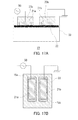
- FIG. 17A is a schematic side view of a hydrogenation apparatus according to one embodiment.
- FIG. 17B is a schematic tope view according to FIG. 17A .
- FIG. 18 is a schematic illustration of a hydrogenation apparatus according to one embodiment
- FIG. 19 is a schematic illustration of a hydrogenation apparatus according to one embodiment.
- FIG. 20 is a schematic illustration of a hydrogenation apparatus according to one embodiment.
- FIG. 21 is another schematic illustration of the hydrogenation apparatus shown in FIG. 20 .
- FIG. 22 is a schematic illustration of a hydrogenation apparatus according to one embodiment.
- FIG. 23 is a schematic illustration of a hydrogenation apparatus according to one embodiment.
- FIG. 24 is a graph representation showing the results of secondary ion mass spectrometry analysis of element distributions in depth direction performed on an amorphous silicon film before hydrogenation.
- FIG. 25 is a graph representation showing the results of secondary ion mass spectrometry analysis of element distributions in depth direction performed on the amorphous silicon film after hydrogenation.
- FIG. 26 is a graph representation showing measurement results by Raman spectroscopy on amorphous silicon films before hydrogenation.
- FIG. 27 is a graph representation showing measurement results by Raman spectroscopy after hydrogenation.
- FIG. 28 is a schematic illustration for explaining measurement by electron spin resonance.
- FIG. 29 is a graph representation showing measurement results by electron spin resonance.
- FIG. 1 is a schematic illustration showing the hydrogenation apparatus 10 according to the present embodiment.
- the hydrogenation apparatus 10 includes a plasma generation section 20 and a hermetic member 30 .
- the inside of the hermetic member 30 is sealed so as to shut off the air outside the hermetic member 30 .
- the plasma generation section 20 may be arranged inside the hermetic member 30 .
- an amorphous silicon film (non-crystalline silicon film) S is disposed inside the hermetic member 30 . Dangling bonds are present in the amorphous silicon film S.
- the plasma generation section 20 of the hydrogenation apparatus 10 in the present embodiment allows, in the presence of a gas at a pressure around the atmospheric pressure containing a hydrogen gas in at least a partial region inside the hermetic member 30 , the gas at a pressure around the atmospheric pressure containing the hydrogen gas to generate plasma.
- Generation of plasma causes ionization of at least part of the hydrogen gas to generate hydrogen ions.
- the hydrogen ions reach the amorphous silicon film S, the dangling bonds of the amorphous silicon film S terminate, thereby eliminating bonding defects. Plasma treatment is performed in this manner.
- the plasma generation section 20 is prepared first.
- the plasma generation section 20 is capable of applying an electric field or an electromagnetic field.
- the hermetic member 30 is prepared.
- the plasma generation section 20 allows plasma to be generated in the presence of the gas at a pressure around the atmospheric pressure containing the hydrogen gas
- the hermetic member 30 is sealed so as not to allow the air outside the hermetic member 30 to be directly mixed.
- the hermetic member 30 may be generally called a chamber or a glove box capable of maintaining its shape even when the inside thereof is vacuumed (strictly, reduced in pressure).
- the hermetic member 30 may allow a gas to pass through the inside thereof as fluid.
- the hermetic member 30 may be tubular in shape.
- the amorphous silicon film S is placed inside the hermetic member 30 .
- the amorphous silicon film S is supported by a substrate, for example.
- the amorphous silicon film S may be placed at a position where the electric field or the electromagnetic filed is applied by the plasma generation section 20 . Alternatively, it may be placed at a position apart from the position where the electric field or the electromagnetic filed is applied by the plasma generation section 20 .
- the plasma generation section 20 allows the gas at a pressure around the atmospheric pressure containing the hydrogen gas to generate plasma in at least a partial region inside the hermetic member 30 .
- the plasma treatment can be performed in this manner.
- bonding defects of the amorphous silicon film S can be easily eliminated.
- the hydrogenation can be recognized by secondary ion mass spectrometry, Raman spectroscopy, or electron spin resonance.
- plasma is generated when the gas containing the hydrogen gas is at a pressure around the atmospheric pressure. This can suppress an increase in kinetic momentum of the hydrogen ions, thereby reducing physical damage to the amorphous silicon film S.
- the partial pressure of the hydrogen gas can be comparatively high, the hydrogenation can be performed within a comparatively short period of time.
- plasma is generated at a pressure around the atmospheric pressure. This can easily avoid batch treatment.
- the pressure of the gas containing the hydrogen gas in generating plasma is around the atmospheric pressure.
- the pressure of the gas containing the hydrogen gas is 0.1 atm or higher and 2 atm or lower, and preferably roughly 1 atm (101325 Pa).
- the gas to which the electric or electromagnetic field is applied in the hermetic member 30 contains only the hydrogen gas.
- another gas may be contained in the gas to which the electric or electromagnetic field is applied, in addition to the hydrogen gas.
- the gas containing hydrogen may be supplied to the hermetic member 30 in the presence of another gas in the hermetic member 30 .
- the supplied gas may be the hydrogen gas only or a gas containing another gas in addition to the hydrogen gas.
- the gas other than the hydrogen gas contained in the mixed gas does not adversely affect the property of the amorphous silicon film S.
- the mixed gas may contain an inert gas in addition to the hydrogen gas.
- the inert gas may be, for example, a rare gas included in Group 18 elements, such as helium, neon, argon, krypton, etc. Further, a nitrogen gas may be used as the inert gas.
- a plurality of the above mentioned rare gases may be mixed in combination as the inert gas contained in the mixed gas.
- the concentration of the hydrogen gas in the mixed gas is preferably 0.1 weight % or higher. It is noted that the mixed gas preferably contains no oxygen gas.
- the mixed gas may contain a gas containing a p-type or n-type impurity element in place of the inert gas or in addition to the inert gas. Provision of such an impurity element to the amorphous silicon film S can result in control of the property of the amorphous silicon film S.
- the mixed gas contains diborane, a p-type amorphous silicon film can be formed.
- the mixed gas contains phosphine or arsine, an n-type amorphous silicon film can be formed.
- the gas containing the hydrogen gas at a pressure around the atmospheric pressure generates plasma in the chamber 30 in which the amorphous silicon film S is provided in the present embodiment.
- a predetermined gas containing the hydrogen gas may be supplied after the atmosphere (the air) inside the chamber 30 is once removed.
- the amorphous silicon film S may be formed in the chamber 30 after the predetermined gas is supplied into the chamber 30 up to the time when the pressure becomes around the atmospheric pressure.
- the predetermined gas may be supplied into the chamber 30 so that the pressure becomes around the atmospheric pressure after the amorphous silicon film S is placed inside the chamber 30 . It is noted that in the case where the amorphous silicon film S is formed after the predetermined gas is supplied, the plasma may be generated immediately after formation of the amorphous silicon film S without substantial gas change in the chamber 30 .
- the plasma generation section 20 generates the electric or electromagnetic field.
- the electric current flowing in the plasma generation section 20 may be direct current or alternating current.
- the frequency of the electric current is zero or higher and 2.45 GHz or lower.
- the frequency of the electric current is further preferably 50 Hz or higher and 100 MHz or lower, and more preferably 1 kHz or higher and 100 kHz or lower.
- the alternating voltage may have a waveform of any of a sine wave, a triangular wave, and a rectangular wave.
- the plasma can be generated sufficiently at a duty ratio of 1% or higher. It is noted that the duty ratio is preferably 5% or higher, and more preferably 25% or higher.
- the ionized gas density at plasma generation varies depending on the electric current and its frequency in the plasma generation section 20 .
- the discharge state varies depending not only on the voltage and the frequency but also on the structure of the plasma generation section 20 , the gas to which the electric or electromagnetic field is applied, etc.
- the electron temperature is different from the ion temperature depending on ionized gas density. For example, where the degree of ionization is low (weakly ionized state), neutral molecules are dominant even where plasma is generated. This plasma may be called weakly ionized plasma or low temperature plasma. It is noted that the mass of the ions are markedly different from that of electrons, and therefore, energy exchange hardly occurs even if ions collide with electrons. For this reason, the electron temperature is different from the ion temperature in the weakly ionized state. For example, the ion temperature is around the room temperature, while the electron temperature is about several thousand degrees to ten thousand degrees.
- the gas is in a state of ionized gas
- the gas does not have enough energy to increase the temperature of the substrate that supports the amorphous silicon film S. Accordingly, the substrate can be handled at low temperatures.
- a glass substrate or a plastic substrate can be used as the substrate that supports the amorphous silicon film S.
- an increase in degree of ionization reduces the ratio of the neutral molecules.
- a further increase in degree of ionization results in almost all gaseous molecules ionized. That is, almost all part of the gas is composed of the ions and the electrons.
- This plasma may be called fully ionized plasma or high temperature plasma. In this case, the electron temperature increases to several ten thousand degrees or higher, and the ion temperature also increases.
- control of the plasma to be generated can control the temperature of the substrate that supports the amorphous silicon film S.
- the temperature of the surface of the amorphous silicon film S can be increased to perform annealing.
- the ion temperature is set comparatively low, variation in internal temperature of the amorphous silicon film S and of the support member thereof can be reduced.
- the electron temperature and the ion temperature can be controlled in the range from the room temperature to the temperature of the surface of the sun.
- the substrate that supports the amorphous silicon film S can have any corresponding shape, and the temperature of the substrate can be controlled.
- control of the ionized gas density can set the electron temperature to be equal to or higher than one hundred thousand degrees and can keep the temperature of part where the hydrogenation is performed comparatively low.
- plasma may be generated with the temperature of the substrate increased using a heater (not shown), such as a hotplate or the like. In this case, the crystallization state can be controlled, while bonding defects can be eliminated.
- the temperature of the substrate at plasma generation is preferably set in the range from minus 30° C. to 900° C. Although it depends on the thickness of the substrate, the temperature of the substrate at plasma generation is preferably set at 300° C. or lower, and more preferably at 250° C. or lower.
- the amorphous silicon film S may be moved at plasma generation so as to pass in the vicinity of the plasma generation section 20 .
- the amorphous silicon film S may be disposed on a slide part that passes in the vicinity of the plasma generation section 20 at plasma generation. In this manner, scanning of the amorphous silicon film S relative to the plasma generation section 20 can eliminate bonding defects in the amorphous silicon film S and can control the configuration thereof.
- the plasma generation section 20 may be moved relative to the amorphous silicon film S.
- the amorphous silicon film S may be moved with the plasma generation section 20 fixed.
- the plasma generation section 20 may be moved with the amorphous silicon film S fixed.
- the amorphous silicon film S may be formed by chemical vapor deposition (CVD). Further, although details will be described later, the amorphous silicon film S may be formed by applying a solution in which a silane compound is dissolved. In this solution, silane-based oligomer or silane-based polymer is dissolved, for example. The solution of the silane compound is applied by spin coating or inkjetting, for example. Further, after the amorphous silicon film S is formed, temporary baking may be performed on the amorphous silicon film S before the plasma generation to remove residual solvent. Alternatively, light may be irradiated to the applied solution before the plasma generation. It is noted that the solution of the silane compound, which may be unstable in the air containing an oxygen gas, is preferably treated inside a globe box under a nitrogen atmosphere.
- a polymer with a five-membered ring may be used as the silane compound.
- polymer may be cross linked by irradiating ultraviolet light. Further, in this case, crosslinking of the polymer can be promoted by the plasma.
- the ionized gas density is too high, silicon-to-silicon bonding may be broken to form dangling bonds. Accordingly, it is preferable to appropriately adjust the ionized gas density.
- hydrogenation can be easily performed without using a comparatively expensive high vacuum system.
- the hydrogenation apparatus in the present embodiment can generate thermal particles by increasing the ionized gas density, thereby achieving promotion of crystallization of the amorphous silicon film.
- the hydrogenation in the present embodiment may be employed as annealing in place of the process of laser treatment.
- the present embodiment can efficiently eliminate bonding defects of the amorphous silicon film S and can promote crystallization of the amorphous silicon film S, thereby increasing the mobility.
- the gas inside the hermetic member 30 may be supplied from the outside.
- a gas supply pipe 32 may be mounted at the hermetic member 30 to fill the hermetic member 30 almost uniformly with the gas containing the hydrogen gas which is supplied from the gas supply pipe 32 .
- the end part of the gas supply pipe 32 may reach the inside of the hermetic member 30 to supply the gas containing the hydrogen gas so that the concentration of the hydrogen gas in the vicinity of the plasma generation section 20 becomes comparatively high.
- the gas containing the hydrogen gas may be supplied locally to the plasma generation section 20 from the gas supply pipe 32 with the hermetic member 30 set almost in a nitrogen atmosphere as a whole so that the plasma generation section 20 allows the gas to generate plasma.
- the hermetic member 30 may be tubular in shape so that the gas containing the hydrogen gas passes inside the hermetic member 30 . It is noted that the amorphous silicon film S herein is disposed inside the hermetic member 30 , while the plasma generation section 20 is arranged outside the hermetic member 30 .
- the hydrogenation apparatus 10 One example of the hydrogenation apparatus 10 according to the present embodiment will be described below. It is noted that while the plasma generation section 20 herein allows plasma to be generated between two electrodes as one example, the plasma generation section 20 may generate plasma by any method.
- FIG. 4 is a schematic illustration of a hydrogenation apparatus 10 according to the present embodiment.
- the plasma generation section 20 is arranged inside the hermetic member 30 .
- a chamber inside which space shut off from the outside air is used as the hermetic member 30 .
- the plasma generation section 20 includes electrodes 21 a , 21 b .
- the amorphous silicon film S is disposed inside the chamber 30 .
- the electrodes 21 a , 21 b are each formed of a conductive member (e.g., metal).
- the electrodes 21 a , 21 b may have a plate-like shape or a specified shape.
- respective parts of the electrodes 21 a , 21 b may have a bulk shape or a mesh-like shape.
- the electrode 21 a may be referred to as a first electrode 21 a
- the electrode 21 b may be referred to as a second electrode 21 b.
- the amorphous silicon film S is disposed between the electrode 21 a and the electrode 21 b herein.
- the amorphous silicon film S may be disposed on the principal surface of the electrode 21 a or 21 b .
- voltage is applied between the electrode 21 a and the electrode 21 b in the state when the gas containing the hydrogen gas is set at a pressure around the atmospheric pressure in the chamber 30 . This generates ionized gas in the chamber 30 .
- the electrode 21 a and the electrode 21 b may be referred collectively to an ionized gas generation section 21 x.
- the chamber 30 is prepared. Inside the chamber 30 , the electrodes 21 a , 21 b and the amorphous silicon film S are disposed. Here, the amorphous silicon film S is disposed on the principal surface of the electrode 21 b .
- the amorphous silicon film S may be supported by another member (not shown), such as a substrate. Dangling bonds are present in the amorphous silicon film S.
- the gas containing the hydrogen gas is set at a pressure around the atmospheric pressure in the chamber 30 .
- voltage is applied between the first electrode 21 a and the second electrode 21 b , thereby generating plasma.
- At least part of the hydrogen gas in the chamber 30 is ionized by the plasma generation.
- the oxygen concentration in the chamber 30 is preferably low at plasma generation. Further, it is preferable to once set the inside of the chamber 30 to be in an almost vacuum state before the gas containing the hydrogen gas is supplied to the chamber 30 .
- alternating voltage is applied between the electrodes 21 a and 21 b .
- one of the electrodes 21 a , 21 b may be grounded, while the potential of the other electrode 21 a or 21 b only may vary.
- the alternating voltage may be supplied to the electrode 21 a , while the electrode 21 b is grounded.
- the alternating voltage is 100 kilovolts or lower, and its frequency is 100 kilohertz or lower, the state of low temperature plasma can be easily achieved, thereby suppressing an increase in temperature of the amorphous silicon film and its support member.
- the alternating voltage is preferably 100 kilovolts or lower.
- the alternating voltage is preferably 25 volts or higher and 100 kilovolts or lower, more preferably 1 kilovolts or higher and 100 kilovolts or lower, further preferably 1 kilovolts or higher and 50 kilovolts or lower, and even more preferably 1 kilovolt or higher and 20 kilovolts or lower.
- the frequency of the alternating voltage is preferably 60 hertz or higher and 1 megahertz or lower.
- the frequency of the alternating voltage is preferably 100 kilohertz or lower, more preferably 1 kilohertz or higher and 100 kilohertz or lower, further preferably 1 kilohertz or higher and 50 kilohertz or lower, and even more preferably 1 kilohertz or higher and 20 kilohertz or lower.
- the alternating voltage and its frequency are low, stable plasma may not be generated.
- the voltage and the frequency are lowered to target values after the alternating current is set at high voltage and high frequency to generate plasma once, stable plasma can be generated comparatively easily at comparatively low alternating voltage and frequency.
- the ionized gas density at plasma generation varies according to the alternating voltage applied to the electrodes 21 a , 21 b and its frequency.
- the discharge state varies depending not only the alternating voltage and the frequency but also the structure of the electrodes 21 a , 21 b , the distance between the electrodes 21 a , 21 b , the gas in the chamber 30 , etc.
- the amorphous silicon film S is disposed at the position where the electric or electromagnetic field is applied by the plasma generation section 20 in the hydrogenation apparatus 10 shown in FIG. 4 .
- the hydrogenation is performed on the amorphous silicon film S by the plasma generated using the plasma generation section 20 .
- This plasma may be called direct plasma.
- the amorphous silicon film S may be disposed at a position other than the position where the electric or electromagnetic field is applied by the plasma generation section 20 .
- the hydrogenation is performed on the amorphous silicon film S also by the plasma generated using the plasma generation section 20 . This plasma may be called remote plasma.
- the amorphous silicon film S may be moved at plasma generation so as to pass between the electrodes 21 a and the electrode 21 b .
- the amorphous silicon film S may be placed on a slide part that passes between the electrode 21 a and the electrode 21 b at plasma generation.
- the electrodes 21 a , 21 b may be moved relative to the amorphous silicon film S.
- the amorphous silicon film S may be moved with the electrodes 21 a , 21 b fixed.
- the electrodes 21 a , 21 b may be moved with the amorphous silicon film S fixed.
- the electrodes 21 a , 21 b are arranged opposite to each other inside the chamber 30 , thereby achieving comparatively high ionized gas density.
- a dielectric may be provided between the electrodes 21 a , 21 b , as needed.
- FIG. 6 is a schematic illustration of a hydrogenation apparatus 10 according to one embodiment.
- a dielectric 22 is provided between the electrode 21 a and the electrode 21 b .
- the dielectric 22 is made of glass. With the use of the dielectric 22 , low temperature plasma can be easily realized.
- the dielectric 22 has a thickness of preferably 0.1 mm or larger, more preferably 1 mm or larger, and even more preferably 3 mm or larger.
- the dielectric 22 is made of an ordinary material with no conductivity.
- the dielectric 22 may be made of an inorganic material or an organic material.
- the dielectric 22 may be made of an inorganic material, such as aluminum oxide, silicon oxide, silicon nitride, etc. Further, examples of the inorganic material include glass, alumina, and apatite.
- the dielectric 22 may be made of an organic material, such as silicon resin, phenol resin, polyimide resin, polytetrafluoroethylene, etc. Further, examples of the organic material include polyimide, polyoxymethylene, and novolac resin.
- insulating metal oxide may be used as a material of the dielectric 22 .
- an aluminum oxide (alumina) plate may be used as the dielectric 22 .
- One of the electrodes 21 a , 21 b may be mounted at the dielectric 22 .
- the electrode 21 a may be mounted at the dielectric 22 .
- the principal surface of the dielectric 22 may be larger than that of each electrode 21 a , 21 b , and the dielectric 22 may have a plate-like shape.
- the electrode 21 a may be formed of a metal mesh or a metal plate.
- the electrode 21 a is attached to the dielectric 22 so as not to extend beyond the dielectric 22 , and the electrode 21 a is arranged opposite to the electrode 21 b with the dielectric 22 interposed therebetween.
- the electrode 21 a is attached to the dielectric 22 by means of an insulating tape.
- the distance between the amorphous silicon film S and the electrode 21 a it is preferable to set the distance between the amorphous silicon film S and the electrode 21 a not to be too short. For example, it is preferable to dispose the amorphous silicon film S 0.5 mm or more apart from the electrode 21 a.
- the electrode 21 a is mounted at the dielectric 22 , but the present invention is not limited to this arrangement.
- the electrodes 21 a , 21 b may be mounted at dielectrics.
- FIG. 7A is a schematic illustration of the hydrogenation apparatus 10 .
- FIG. 7B is a schematic illustration of the electrode 21 a as viewed from above.
- FIG. 7C is a schematic illustration of the electrode 21 b as viewed from below.
- the electrode 21 a is mounted at the dielectric 22 a
- the electrode 21 b is mounted at the dielectric 22 b.
- the dielectric 22 a is arranged opposite to the dielectric 22 b , and the electrodes 21 a , 21 b are arranged outward of the dielectrics 22 a , 22 b , respectively.
- the amorphous silicon film S is disposed on the principal surface other than the principal surface of the dielectric 22 b at which the electrode 21 b is mounted so as to be overlap with the electrode 21 b.
- the electrodes 21 a , 21 b are arranged so as to be different in height from the ground (i.e., in vertical direction).
- the electrode 21 b located below is grounded.
- electric current is supplied through a lead wire from a power source 50 installed outside the chamber 30 .
- the grounded electrode 21 b may be referred to as a ground electrode, while the other electrode 21 a may be referred to as a discharge electrode.
- the electrodes 21 a , 21 b may be mounted at the dielectrics 22 a , 22 b so as not to extend beyond the dielectrics 22 a , 22 b , respectively, and the dielectric 22 a , 22 b may be arranged opposite to each other in the direction where the electrodes 21 a , 21 b are not opposed to each other.
- aluminum oxide substrates may be used as the dielectrics 22 a , 22 b .
- each principal surface of the aluminum oxide substrates 22 a , 22 b is nearly square in shape with a length of about 10 cm and has a thickness of about 0.5 mm.
- square stainless meshes with a length of 5 cm are used as the electrodes 21 a , 21 b , and the stainless meshes 21 a , 21 b are attached to the aluminum oxide substrates 22 a , 22 b , respectively, by means of an insulating tape.
- the distance between the dielectrics 22 a , 22 b is set according to the thickness of the dielectrics 22 a , 22 b and the voltage applied between the electrodes 21 a , 21 b .
- the distance between the dielectrics 22 a , 22 b is preferably 1 mm or larger in order to avoid short-circuit discharge.
- the electrode 21 b of the electrodes 21 a , 21 b which is arranged below, is grounded, while the electrode 21 a arranged above is connected to the power source 50 .
- the present invention is not limited to this configuration. It is possible that the electrode 21 b arranged below is connected to the power source 50 , while the electrode 21 a arranged above is ground.
- the discharge electrode 21 a and the ground electrode 21 b are mounted at the dielectrics 22 a , 22 b , respectively, in FIG. 7 , which does not limit the present invention. As shown in FIG. 8 , only the discharge electrode 21 a may be mounted at the dielectric 22 . Alternatively, as shown in FIG.
- only the ground electrode 21 b may be mounted at the dielectric 22 . Further, as shown in FIG. 10 , it is possible that the two electrodes 21 a , 21 b are not mounted at the dielectrics 22 a , 22 b , but face each other with the gas containing the hydrogen gas allowed to intervene and with no dielectrics interposed therebetween.
- the electrode 21 a may include a plurality of conduction parts extending in stripes.
- the electrode 21 b may include a plurality of conduction parts extending in stripes.
- the ionized gas density can be controlled with high accuracy. Control of the ionized gas density can easily suppress an increase in temperature of the amorphous silicon film S. Further, since elimination of bonding defects of and change in configuration of the amorphous silicon film S can be achieved at a position where ionized gas is generated, plasma may be generated so that the ionized gas performs scan across the amorphous silicon film S. As such, the electrodes 21 a , 21 b may be formed linearly.
- the dielectric(s) 22 may or may not be provided to the electrodes 21 a , 21 b .
- the electrodes 21 a , 21 b may be the same or different in shape.
- one of the electrodes 21 a , 21 b may be in plate-like shape, while the other may be linear.
- FIG. 11 a hydrogenation apparatus 10 will be described in which linear electrodes 21 a , 21 b are mounted at dielectrics 22 a , 22 b , respectively.
- FIG. 11A is a schematic illustration of the hydrogenation apparatus 10 .
- FIG. 11B is a schematic illustration of the electrode 21 a as viewed from above.
- FIG. 11C is a schematic illustration of the electrode 21 b as viewed from below.
- the dielectric 22 a to which the electrode 21 a is attached is arranged opposite to the dielectric 22 b to which the electrode 21 b is attached.
- the electrode 21 b is also grounded herein.
- Each of the electrodes 21 a , 21 b is a linear electrode and includes at least two or more conduction parts extending in stripes. With the linear electrodes 21 a , 21 b , the ionized gas density can be controlled easily.
- the linear electrodes 21 a , 21 b may be formed by processing a metal plate or a metal mesh.
- the hydrogenation apparatus 10 shown in FIG. 11 has a configuration in which the electrodes 21 a , 21 b are mounted at the dielectrics 22 a , 22 b , respectively, which does not limit the present invention. Only one of the electrodes 21 a , 21 b may be mounted at a dielectric. For example, the electrode 21 a may be mounted at a dielectric 22 with the electrode 21 b not mounted at a dielectric.
- FIG. 12A is a schematic illustration of the hydrogenation apparatus 10 .
- FIG. 12B is a schematic illustration of the electrode 21 a as viewed from above.
- FIG. 12C is a schematic illustration of the electrode 21 b as viewed from below.
- the electrode 21 a herein is mounted at the dielectric 22 , while the electrode 21 b is not mounted at a dielectric.
- the electrode 21 b is arranged opposite to the dielectric 22 at which the electrode 21 a is mounted. Further, the electrode 21 a is a linear electrode, while the grounded electrode 21 b has a plate-like shape.
- the electrode 21 b is not mounted at a dielectric, while the electrode 21 a is mounted at the dielectric 22 , which does not limit the present invention.
- the electrode 21 b may be mounted at the dielectric 22 with the electrode 21 a not mounted at a dielectric.
- FIG. 13 a hydrogenation apparatus 10 which includes an electrode 21 a which is not mounted at a dielectric and an electrode 21 b which is mounted at a dielectric 22 .
- FIG. 13A is a schematic illustration of the hydrogenation apparatus 10 .
- FIG. 13B is a schematic illustration of the electrode 21 a as viewed from above.
- FIG. 13C is a schematic illustration of the electrode 21 b as viewed from below.
- the dielectric 22 at which the electrode 21 b is mounted is arranged opposite to the electrode 21 a .
- the electrode 21 a has a plate-like shape, while the grounded electrode 21 b is a linear electrode.
- the electrodes 21 a , 21 b are mounted at the dielectric 22 , and the electrodes 21 a , 21 b are arranged opposite to each other with the dielectric 22 interposed therebetween, which does not limit the present invention.
- the electrodes 21 a , 21 b may be arranged opposite to each other with intervention of the gas containing the hydrogen gas with no dielectric interposed therebetween and with neither the electrode 21 a nor the electrode 21 b being mounted at a dielectric.
- FIG. 14A is a schematic illustration of the hydrogenation apparatus 10 .
- FIG. 14B is a schematic illustration of the electrode 21 a as viewed from above.
- FIG. 14C is a schematic illustration of the electrode 21 b as viewed from below.
- the electrode 21 a is a linear electrode, while the grounded electrode 21 b has a plate-like shape.
- the electrode 21 a is a linear electrode, while the electrode 21 b has a plate-like shape, which does not limit the present invention.
- the electrode 21 a may have a plate-like shape, while the electrode 21 b may be a linear electrode.
- FIG. 15A is a schematic illustration of a hydrogenation apparatus 10 .
- FIG. 15B is a schematic illustration of an electrode 21 a as viewed from above.
- FIG. 15C is a schematic illustration of an electrode 21 b as viewed from below.
- the electrode 21 a has a plate-like shape, while the grounded electrode 21 b is a linear electrode.
- At least one of the electrodes 21 a , 21 b is a linear electrode including the conductive parts which extend in parallel to each other in stripes and are connected to different conductive parts, which does not limit the present invention.
- the linear electrode may include branch portions extending in stripes in a direction parallel to a given direction from one trunk part to have a comb-like shape.
- comparatively thin plate-shaped or linear conductive members are used as the electrodes 21 a , 21 b , which does not limit the present invention.
- FIG. 16 is a schematic illustration of one electrode 21 in a hydrogenation apparatus 10 .
- the electrode 21 herein has a rod shape.
- the electrode 21 is formed of a rod-shaped metal.
- the electrode 21 is disposed inside a tubular dielectric 22 .
- the dielectric 22 is made of an insulating material, e.g., an organic insulator.
- the area for ionized gas generation can be comparatively easily controlled.
- the organic insulator formed in tubular shape polytetrafluoroethylene, polyethylene, or vinyl chloride may be used, for example.
- examples of the rod-shaped metal include a stainless wire, a copper wire, a silver wire, a gold wire, etc.
- a copper wire may be used as the electrode 21 , and the copper wire may be covered with polytetrafluoroethylene.
- the discharge electrode 21 a may be formed as the thus covered electrode 21 , while the ground electrode 21 b of a metal mesh or a metal plate may be mounted at the dielectric 22 b .
- the amorphous silicon film S is arranged preferably 0.5 mm or more apart from the electrode 21 a .
- the ground electrode 21 b may be formed as the thus covered electrode 21 , and the discharge electrode 21 a of a metal mesh or a metal plate may be mounted at the dielectric 22 a.
- the discharge electrode 21 a may be formed as the thus covered electrode 21
- the ground electrode 21 b may be formed of a metal mesh or a metal plate.
- the ground electrode 21 b may be formed as the thus covered electrode 21
- the discharge electrode 21 a may be formed of a metal mesh or a metal plate.
- the gas containing the hydrogen gas generates plasma at a pressure around the atmospheric pressure in the chamber 30 .
- the hydrogen ions ionized by the plasma can terminate the dangling bonds of the amorphous silicon film S to eliminate bonding defects.
- the configuration of the amorphous silicon film S can be controlled in addition to elimination of bonding defects.
- the amorphous silicon film S can be formed in which an amorphous state and crystalline state are mixed.
- the region where the ionized gas is generated is defined by the area of the electrodes 21 a , 21 b . Accordingly, changing the electrodes 21 a , 21 b can result in control of the region where the hydrogenation is performed. For example, where the amorphous silicon film is formed on an insulating layer, heat may be stored in the insulating layer to degrade its insulating property. However, appropriate change of the electrodes 21 a , 21 b can suppress such thermal damage.
- plasma is generated between the electrodes 21 a , 21 b , and the amorphous silicon film S is disposed between the electrodes 21 a , 21 b in the above description, which does not limit the present invention.
- FIG. 17A is a schematic side view of a hydrogenation apparatus 10 according to one embodiment.
- FIG. 17B is a schematic tope view thereof.
- electrodes 21 a , 21 b may be arranged on one of the principal surfaces of a dielectric 22 , and plasma may be generated in the vicinity of the other principal surface of the dielectric 22 . Such discharge may be called surface discharge.
- the electrodes 21 a , 21 b are disposed on one of the principal surfaces of the dielectrics 22 with a predetermined space left.
- Each of the electrodes 21 a , 21 b is a metal plate or a metal mesh.
- the electrode 21 a is covered with an insulating material 23 a
- the electrode 21 b is covered with an insulating material 23 b . Accordingly, direct discharge can be prevented from occurring between the electrode 21 a and the electrode 21 b .
- organic resin may be used for the insulating materials 23 a , 23 b , for example.
- epoxy resin may be used for the organic resin.
- the distance between the electrode 21 a and the electrode 21 b is adjusted according to the applied voltage.
- the distance between the electrode 21 a and the electrode 21 b is about 2 cm.
- Voltage application to the above electrodes 21 a , 21 b can ionize the gas in the vicinity of the principal surface different from the principal surface of the dielectric 22 at which the electrode 21 a , 21 b are mounted.
- the hydrogenation is performed by allowing the amorphous silicon film S to pass in the region where the ionized hydrogen gas is formed by surface discharge.
- a substrate on which the amorphous silicon film S is provided may be scanned relative to the electrodes 21 a , 21 b that are fixed.
- the electrodes 21 a , 21 b may be scanned relative to a fixed substrate on which the amorphous silicon film S is provided.
- the hydrogenation apparatus 10 can perform the hydrogenation by scanning the ionized gas generation section 21 x (see FIG. 4 ) relative to the substrate.
- hydrogenation can be performed by scanning the substrate with the ionized gas generation section 21 x fixed.
- abnormal discharge may occur when the amorphous silicon film S is disposed between the electrode 21 a and the electrode 21 b .
- the insulating layer typically, an insulating layer made of silicon oxide or silicon nitride
- the insulating layer may be broken down upon occurrence of abnormal discharge.
- plasma may be generated between the electrodes 21 a , 21 b by applying voltage between the electrode 21 a and the electrode 21 b in the state where the gas inside the chamber 30 is allowed to flow so as to pass between the electrode 21 a and the electrode 21 b and reach the amorphous silicon film S.
- the amorphous silicon film S is not disposed in the electric field, damage to the amorphous silicon film S caused due to abnormal discharge can be suppressed.
- FIG. 18 is a schematic illustration of a hydrogenation apparatus 10 .
- the hydrogenation apparatus 10 shown in FIG. 18 is configured such that the amorphous silicon film S is disposed at a position other than the position between the electrode 21 a and the electrode 21 b , and the gas containing the hydrogen gas flows from the gas supply pipe 32 through between the electrode 21 a and the electrode 21 b and then reaches the amorphous silicon film S.
- the electrode 21 a is connected to the power source 50 , while the electrode 21 b is grounded.
- the gas containing the hydrogen gas passes through between the electrode 21 a and the electrode 21 b , while the electric current is supplied to the electrode 21 a to apply voltage between the electrode 21 a and the electrode 21 b , the hydrogen gas is ionized, thereby generating plasma.
- the ionized hydrogen gas reaches the amorphous silicon film S to cause hydrogenation.
- the plasma generated in this manner may be called remote plasma.
- FIG. 19 is a schematic illustration of a hydrogenation apparatus 10 .
- through holes 210 are formed in an electrode 21 a .
- This hydrogenation apparatus 10 is configured such that the gas containing the hydrogen gas passes from the upper side of the electrode 21 a through the through holes 210 of the electrode 21 a and then reaches between the electrode 21 a and an electrode 21 b.
- plasma is generated using the gas inside the chamber 30 in the above description, which does not limit the present invention.
- the plasma may be generated using the gas introduced into the chamber 30 .
- FIGS. 20 and 21 are schematic illustrations of a hydrogenation apparatus 10 according to one embodiment.
- the hydrogenation apparatus 10 is of single chamber type.
- the hydrogenation apparatus 10 includes electrodes 21 a , 21 b , dielectrics 22 a , 22 b , and a spacer 24 .
- the electrode 21 b which cannot be seen because it is covered with the dielectric 22 b , is connected to a ground terminal Tb through a ground wire Lb.
- the electrode 21 a is arranged above the electrode 21 b .
- the electrode 21 a is connected to a power source terminal Ta through a high voltage wire La.
- each electrode 21 a , 21 b is used as each electrode 21 a , 21 b
- alumina plate is used as each dielectric 22 a , 22 b
- each entire surface of the end parts of the electrodes 21 a , 21 b may be covered with a tape.
- a polyimide tape may be used as the tape.
- the dielectric 22 a and the dielectric 22 b in this hydrogenation apparatus 10 are arranged with the spacer 24 interposed therebetween.
- the spacer 24 has a length that can set the distance between the dielectric 22 a and the amorphous silicon film S (not shown in FIGS. 20 and 21 ) disposed on the dielectric 22 b to be 0.5 mm or larger. It is noted that a spacer 25 is provided between the bottom surface of the chamber 30 and the electrode 21 b so that the electrode 21 b is spaced a predetermined distance apart from the bottom surface of the chamber 30 .
- the chamber 30 includes a suction port 32 a used for sucking out the gas inside the chamber 30 and a supply port 32 b used for introducing the gas into the chamber 30 .
- the suction port 32 a may be connected to a vacuum pump, and the supply port 32 b may be connected to a gas canister filled with the mixed gas.
- a pressure gauge 32 c indicative of the pressure inside the chamber 30 is mounted at the chamber 30 .
- FIG. 21 is another schematic illustration of the hydrogenation apparatus 10 shown in FIG. 20 .
- the spacers 24 , 25 are omitted herein.
- the electrodes 21 a , 21 b are attached to almost the centers of the principal surfaces of the dielectrics 22 a , 22 b , respectively.
- the electrode 21 a is arranged above, while the electrode 21 b is arranged below.
- the electrodes 21 a , 21 b are arranged so as to face outward of the dielectrics 22 a , 22 b , respectively.
- the mixed gas is introduced into the chamber 30 through a gas canister 34 . Further, the air inside the chamber 30 is removed using a vacuum pump 36 .
- the power source 50 includes a waveform controller 52 and a voltage amplifier 54 .
- the waveform controller 52 outputs a signal indicative of voltage with a controlled waveform.
- the voltage amplifier 54 generates an output signal obtained by amplifying the voltage of the signal from the waveform controller 52 .
- the waveform controller 52 outputs a signal having a voltage of 100 volts.
- the voltage amplifier 54 amplifies the voltage of the waveform controller 52 by 1000 times to generate a signal having a voltage of 10 kilovolts and a frequency of 10 kilohertz.
- the electrode 21 a is connected to the voltage amplifier 54 .
- the electrode 21 b is connected to the ground.
- the chamber 30 inside which the electrodes 21 a , 21 b and the amorphous silicon film S (not shown herein) are disposed is sealed, and the air inside the chamber 30 is removed (degassed) using the vacuum pump 36 . Then, a mixed gas is introduced into the chamber 30 from the gas canister 34 .
- the mixed gas contains helium and hydrogen. Degassing and mixed gas introduction may be repeated plural times. It is noted that mixed gas introduction as above can prevent contamination in the chamber 30 with an impurity and can control the condition inside of the chamber 30 at plasma generation.
- alternating current at high voltage and high frequency is supplied between the electrode 21 a and the electrode 21 b to ionize at least part of the mixed gas, thereby generating plasma.
- amorphous silicon film S disposed inside the chamber 30 hydrogenation of the amorphous silicon film S is performed by the ionized hydrogen gas.
- bonding defects of the amorphous silicon film S can be eliminated.
- the temperature of the amorphous silicon film S at plasma generation can be adjusted according to the structure of the electrodes, the mixed gas, and the voltage between the electrodes 21 a , 21 b .
- the amorphous silicon film S may be damaged by heat at plasma generation.
- changing the structure of the electrodes can change the ionized gas density, thereby controlling damage to the amorphous silicon film S caused by the heat.
- the hydrogenation apparatus 10 can eliminate bonding defects by generating plasma. It is noted that such defects may be induced when a polycrystalline semiconductor film is formed by laser irradiation and when an impurity element is implanted to a semiconductor film. However, the hydrogenation apparatus 10 according to the present embodiment can be suitably used also for elimination of defects (lattice defects) induced in this way.
- the plasma generation section 20 allows plasma to be generated by the electric filed formed between the two electrodes in the above description, which does not limit the present invention.
- the plasma generation section 20 may allow plasma to be generated by an electromagnetic field.
- FIG. 22 is a schematic illustration of a hydrogenation apparatus 10 according to one embodiment.
- a plasma generation section 20 in this hydrogenation apparatus 10 includes a coil 26 .
- the gas containing the hydrogen gas passes inside the hermetic member 30 , and the coil 26 is arranged so as to surround the hermetic member 30 .
- Application of predetermined alternating voltage to the coil 26 generates plasma inside the hermetic member 30 .
- the generated plasma reaches the amorphous silicon film S (not shown herein) to initiate plasma treatment.
- the coil 26 is arranged so as to surround the hermetic member 30 in FIG. 22 , which does not limit the present invention.
- the coil 26 may be arranged outside the end part of the hermetic member 30 .
- FIG. 23 is a schematic illustration of a hydrogenation apparatus 10 according to one embodiment.
- a plasma generation section 20 includes a microwave generating device 27 , a waveguide 28 , and antenna (coil) 29 .
- Microwaves generated in the microwave generating device 27 are transmitted into the hermetic member 30 via the waveguide 28 and the antenna 29 . Transmission of the microwaves generates plasma inside the hermetic member 30 .
- the generated plasma reaches the amorphous silicon film S (not shown herein), thereby initiating plasma treatment.
- the aforementioned hydrogenation apparatus 10 with reference to FIGS. 20 and 21 was used.
- Square metal meshes with a length of about 60 mm were used as the electrodes 21 a , 21 b .
- Alumina plates with a thickness of about 5 mm were used as the dielectrics 22 a , 22 b .
- the metal meshes 21 a , 21 b were attached to almost the centers of the principal surfaces of the alumina plates 22 a , 22 b , respectively.
- Each end surface of the metal meshes 21 a , 21 b was sealed with a polyimide tape.
- the metal mesh 21 a was arranged above, while the metal mesh 21 b was arranged below.
- the metal meshes 21 a , 21 b were arranged so as to face outward of the alumina plates 22 a , 22 b , respectively.
- a Bakelite plate with a thickness of 9.6 mm was used as the spacer 24 .
- the metal meshes 21 a , 21 b and the alumina plates 22 a , 22 b as above were set inside the chamber 30 .
- the electrode 21 a was connected to the high voltage power source 50 through the wire La for high voltage.
- the electrode 21 b was connected to a ground wire.
- the air was replaced by a helium gas at a purity of 99.9999%. After the pressure reduction and the helium gas replacement were repeated twice, the pressure inside the chamber 30 was reduced again to 5.5 ⁇ 10 ⁇ 1 Pascals by using the vacuum pump 36 .
- the mixed gas was a gas obtained by mixing a helium gas and a hydrogen gas at a ratio of 96:4. The mixed gas was filled until the pressure of the mixed gas became around the atmospheric pressure.
- the waveform controller 52 output a signal having a predetermined voltage, and the voltage amplifier 54 amplifies the voltage of the waveform controller 52 by 1000 times to generate an output signal.
- the output voltage of the waveform controller 52 was 1.8 V, 3.5 V, 4.0 V, 4.5 V, and 5.5 V.
- the voltage applied to the metal meshes 21 a was 1.8 kV, 3.5 kV, 4.0 kV, 4.5 kV, and 5.5 kV. It is noted that each voltage waveform was a sine wave, and the frequency of the voltages was 10 kHz. The discharge states under the five conditions different in voltage applied to the metal mesh 21 a were observed.
- Table 1 indicates details of the five different conditions (hereinafter referred to as Conditions 1-5) of the voltages applied to the metal mesh 21 a and the discharge states thereunder. Under these conditions, streamer discharge was formed between the electrodes 21 a , 21 b . Further, it was recognized that the higher the voltage was raised, the more widely the streamer discharge extended between the electrodes 21 a , 21 b . It is noted that glow discharge was not formed at the comparatively high output frequency, 10 kHz.
- the plasma was generated in the manner similar to that in EXAMPLE 1.
- the output voltage of the waveform controller 52 was 1.8 V, 3.5 V, 3.8 V, 4.3 V, 7.0 V, and 8.0 V.
- the voltage applied to the metal mesh 21 a was 1.8 kV, 3.5 kV, 3.8 kV, 4.3 kV, 7.0 kV, and 8.0 kV. It is noted that in each case, the voltage waveform was a sine wave, and the frequency of the voltages was 1 kHz. The discharge states under the six conditions different in voltage applied to the metal mesh 21 a were observed.
- Table 2 indicates details of the six different conditions (hereinafter referred to as Conditions 6-11) of the voltages applied to the metal mesh 21 a and the discharge states thereunder. It was recognized that when the frequency of the voltage was comparatively low, 1 kHz, application of voltage over 3.5 kV to the metal mesh 21 a caused glow discharge.
- the plasma was generated in the manner similar to that in EXAMPLE 1 or 2.
- the output voltage of the waveform controller 52 was 1.8 V, 3.5 V, 3.9 V, 4.3 V, and 7.0 V.
- the voltage applied to the metal mesh 21 a was 1.8 kV, 3.5 kV, 3.9 kV, 4.3 kV, and 7.0 kV. It is noted that in each case, the voltage waveform was a sine wave, and the frequency of the voltages was 0.5 kHz. The discharge states under the five conditions different in voltage applied to the metal mesh 21 a were observed.
- Table 3 indicates details of the five different conditions (hereinafter referred to as Conditions 12-16) of the voltages applied to the metal mesh 21 a and the discharge states thereunder. It was recognized that when the frequency of the voltage was comparatively low, 0.5 kHz, application of voltage over 3.5 kV to the metal mesh 21 a caused glow discharge.
- the plasma was generated in the manner similar to that in EXAMPLES 1-3. Specifically, the distance between the alumina plates 22 a , 22 b was 6.4 mm.
- the output voltage of the waveform controller 52 was 3.5 V, 4.2 V, and 5.3 V.
- the voltage applied to the metal mesh 21 a was 3.5 kV, 4.2 kV, and 5.3 kV. It is noted that in each case, the voltage waveform was a sine wave, and the frequency of the voltages was 10 kHz. The discharge states under the three conditions different in voltage applied to the metal mesh 21 a were observed.
- Table 4 indicates details of the three different conditions (hereinafter referred to as Conditions 17-19) of the voltages applied to the metal mesh 21 a and the discharge states thereunder. It was recognized that even when the frequency of the voltage was comparatively high, 10 kHz, application of voltage over 4.2 kV to the metal mesh 21 a caused glow discharge because of the short distance between the alumina plates 22 a , 22 b , and in turn, between the metal meshes 21 a , 21 b .
- the output voltage of the waveform controller 52 was 2.9 V, 5.2 V, 7.5 V, and 9.0 V.
- the voltage applied to the metal mesh 21 a was 2.9 kV, 5.2 kV, and 7.5 kV, and 9.0 kV. It is noted that in each case, the voltage waveform was a sine wave, and the frequency of the voltages was 1 kHz. The discharge states under the four conditions different in voltage applied to the metal mesh 21 a were observed.
- Table 5 indicates details of the four different conditions (hereinafter referred to as Conditions 20-23) of the voltages applied to the metal mesh 21 a and the discharge states thereunder. It was recognized that even when the frequency of the voltage was comparatively high, 1 kHz, application of voltage of even about 1.8 kV to the metal mesh 21 a could cause glow discharge because of the short distance between the alumina plates 22 a , 22 b , and in turn, between the metal meshes 21 a , 21 b .
- the output voltage of the waveform controller 52 was 3.0 V, 5.0 V, 8.0 V, and 9.0 V.
- the voltage applied to the metal mesh 21 a was 3.0 kV, 5.0 kV, and 8.0 kV, and 9.0 kV. It is noted that in each case, the voltage waveform was a sine wave, and the frequency of the voltages was 0.5 kHz. The discharge states under the four conditions different in voltage applied to the metal mesh 21 a were observed.
- Table 6 indicates details of the four different conditions (hereinafter referred to as Conditions 24-27) of the voltages applied to the metal mesh 21 a and the discharge states thereunder. It was recognized that glow discharge was caused under each condition.
- the amorphous silicon film was formed using a solution of a silane compound.
- the method of synthesizing the amorphous silicon film is disclosed in, for example, U.S. Pat. No. 7,485,691B1. After a catalyst Cp 2 ZrPh 2 was synthesized, poly(phenylsilane) was synthesized to finally obtain poly(hydrosilane).
- dimethyl ether (DME) of 39 mL was poured into a reaction flask with a Cp 2 ZrCl 2 (5.0 g) as a solvent, while the temperature was set between 0 and 10° C.
- a THF solution 34.37 mL
- PhMgBr at a concentration of 37.1 moL/L was dripped, and then was stirred at a temperature of 24-26° C. for 19 hours.
- Et 2 O 8 mL was added and stirred at a temperature of 24-26° C. for one hour.
- Cp 2 ZrPh 2 (0.165 g) was poured into a reaction flask. Then, PhSiH 3 (10 g) was added at a temperature of 24-26° C. and was stirred at the same temperature for 89 hours. Subsequently, after further addition of toluene (47 g), 3% HCl was added (68 g ⁇ 5 times), and stirring, washing, and separation were performed. Thereafter, ion-exchange water (68 g) was added, and stiffing and washing were performed.
- Cyclohexane (43.5 g) was poured into a 100 mL brown reaction flask with poly(phenylsilane) (5.0 g) as a solvent.
- AlCl 3 (0.41 g) was added and the mixture was solidified by liquid nitrogen.
- the solidified mixture was increased in temperature up to the room temperature in a water bath, and was replaced by nitrogen.
- an HCl gas was blown at a flow rate of 950 mL/min for ten hours. Then, pressure reduction and pressure recovery with nitrogen were repeated ten times to remove HCl.
- an Et 2 O (13.72 g) solution containing LAH (1.17 g) was dripped onto the mixture over 30 minutes at a temperature of 0-10° C. After stirring at the room temperature for 12 hours, the reaction solution was poured into ion-exchange water (11 g), was stiffed for one minute, and was left. Then, the supernatant liquor was subjected to decantation. After this water washing was repeated three times, an organic layer was subjected to filtration with a membrane filter, concentration, and drying under reduced pressure, thereby obtaining the target poly(hydrosilane) (0.94 g).
- Hydrosilane obtained by the aforementioned method was dissolved into a cyclopentadiene solution and was prepared to have a concentration of 10 wt %. Then, the solution of 2.5 mL was put into a quartz vessel. Thereafter, light which shows a strong peak at a wavelength of around 300 nm was irradiated to the solution for five seconds with a high-pressure mercury-vapor lamp (4000 mW/cm 2 ) while stiffing the solution, thereby causing cross-linking of polysilane. After the cross-linking, the cross-linked polysilane was spin coated onto a quartz substrate, was held at a temperature of 450° C. for one hour in a nitrogen atmosphere, thereby forming an amorphous silicon film S. In that time, hydrogen in the amorphous silicon film S was removed to produce bonding defects.
- the substrate on which the amorphous silicon film S was formed was placed onto a hotplate for thermal treatment to perform temporary baking on the amorphous silicon film S. Then, the amorphous silicon film S was placed on the ground electrode 21 b.
- the mixed gas herein contained helium and hydrogen, and its hydrogen concentration was about 4%. Subsequently, degassing and introduction of the mixed gas were repeated three times to substantially remove the nitrogen gas inside the chamber 30 .
- FIG. 24 shows the results of element analysis in the depth direction of the substrate before the hydrogenation.
- FIG. 25 shows the results of element analysis in the depth direction of the substrate after the hydrogenation.
- the hydrogen distribution in the thickness direction in the substrate before the hydrogenation was about 2 ⁇ 10 21 (atoms/cm 3 ) or lower.
- the hydrogen distribution in the thickness direction in the substrate after the hydrogenation was increased to about 6.5 ⁇ 10 21 (atoms/cm 3 ). In view of this, it was clarified that the hydrogenation could increase the content in the substrate when compared with that before the hydrogenation.
- Hydrosilane synthesized by the aforementioned method was dissolved into a cyclopentadiene solution and was prepared to have a concentration of 10 wt %. Then, the solution of 2.5 mL was put into a quartz vessel. Thereafter, light which shows a strong peak at a wavelength of around 300 nm was irradiated to the solution for five seconds with a high-pressure mercury-vapor lamp (4000 mW/cm 2 ) while stiffing the solution, thereby causing cross-linking of polysilane. After the cross-linking, the cross-lined polysilane was spin coated onto a quartz substrate, was held at a temperature of 450° C. for one hour in a nitrogen atmosphere, thereby forming an amorphous silicon film S. In that time, hydrogen in the amorphous silicon film S was removed to produce bonding defects.
- a high-pressure mercury-vapor lamp 4000 mW/cm 2
- the substrate on which the amorphous silicon film S was formed was placed onto a hotplate for thermal treatment to perform temporary baking on the amorphous silicon film S. Then, the amorphous silicon film S was placed on the ground electrode 21 b.
- the mixed gas herein contained helium and hydrogen, and its hydrogen concentration was about 4%. Subsequently, degassing and introduction of the mixed gas were repeated three times to substantially remove the nitrogen gas inside the chamber 30 .
- FIG. 26 shows the measurement results by Raman spectroscopy before the hydrogenation.
- FIG. 27 shows the measurement results by Raman spectroscopy after the hydrogenation. While a peak derived from amorphous silicon appeared at around 450 cm ⁇ 1 before the hydrogenation, the hydrogenation caused a peak Pb derived from crystalline silicon to appear at around 500 cm ⁇ 1 in addition to the peak Pa derived from amorphous silicon.
- Silicon ink (10% solid content) of 2004, was poured into an ESR test tube inside a glove box (0.1 ppm or lower oxygen concentration and 1 ppm or lower moisture content). Then, as shown in FIG. 28 , the gas supply pipe 32 was set above (about 3 mm above) the silicon ink within the ESR test tube 30 , and a mixed gas containing a helium gas and a hydrogen gas was introduced therein. The mixed gas was introduced at a rate of about 10 mL/min, and the concentration of the hydrogen gas was about 4%.
- a conductive tape 21 with a width of about 5 mm was wound to the ESR test tube 30 at a level of the tip end of the gas supply pipe 32 , and a high voltage electrode was connected to the conductive tape 21 to apply an alternating voltage of 10 kV at a frequency of 10 kHz.
- plasma generation was allowed to continue at the room temperature for ten minutes.
- the ESR test tube 30 was moved to a baking furnace with plasma generation continued. Thereafter the temperature was raised over one hour from the room temperature to 100° C., and then, baking was further continued for one hour with the temperature kept at 100° C. Subsequently, the temperature was raised over one hour up to 450° C.
- FIG. 29 shows the results measured by ESR. Absorption of microwaves by dangling bonds corresponds to an applied magnetic field of 337 mT. For comparison, FIG. 29 shows the measurement result where no plasma was generated in combination. Further, the applied magnetic field corresponding to a manganese marker for plasma corresponds to 332 mT and 341 mT. In FIG. 29 , the degree of absorption by the manganese marker is shown so as to be equivalent between the presence and the absence of plasma generation. It can be understood from FIG. 29 that plasma generation could significantly reduce bonding defects.
- bonding defects of an amorphous silicon film can be eliminated.
- This amorphous silicon film can be used suitably for semiconductor devices
Abstract
A hydrogenation method according to the present invention includes preparing a plasma generation section (20), preparing a hermetic member (30), disposing an amorphous silicon film (S) inside the hermetic member (30), and performing plasma treatment on the amorphous silicon film (S) in a manner that the plasma generation section (20) allows a gas at a pressure around an atmospheric pressure containing a hydrogen gas to generate plasma in at least a partial region inside the hermetic member (30). Suitably, the disposing an amorphous silicon film (S) includes forming the amorphous silicon film (S) inside the hermetic member (30) with the use of a solution in which a silane compound is dissolved.
Description
The present invention relates to hydrogenation methods and hydrogenation apparatuses.
Semiconductor devices including a silicon film have been widely used for electronic devices, such as display devices, controllers, etc. In general, monocrystalline silicon has high conductivity. Nevertheless, in view of cost and manufacturing processes, an amorphous silicon film or a polysilicon film is usually used as the semiconductor film. However, the amorphous silicon film, which has insufficiently conductivity, is subjected to annealing to improve the property in many cases.
Typically, it is known that thermal annealing is performed on the amorphous silicon film. In the thermal annealing, the amorphous silicon film is exposed to comparatively high temperatures to form the polysilicon film. In general, the amorphous silicon film is exposed to temperatures in the range from 600° C. to 1100° C. for several ten hours in the thermal annealing. It is noted that thermal annealing at a temperature of 500° C. or lower hardly provides effects, and therefore, it is difficult to perform the thermal annealing using a comparatively low-cost and excellently-processable substrate, such as a glass substrate and a plastic substrate, as a substrate for supporting the amorphous silicon film.
Further, laser annealing has been known as another annealing. The laser annealing is performed in such a manner that laser light is irradiated to the amorphous silicon film to form the polysilicon film. In general, the laser annealing can provide comparatively high energy partially to the amorphous silicon film, so that a substrate that supports the silicon film is not exposed to high temperatures as a whole. Accordingly, a glass substrate and a plastic substrate, which have comparatively low thermal resistance, can be used as the substrate.
The laser annealing uses a continuous wave laser or a pulsed laser. In the case using the continuous wave laser, such as an argon ion laser, a light beam having a spot with a diameter of about 100 μm is irradiated to the silicon film, thereby performing scan by the light beam on the silicon film. When irradiation of the light beam melts the silicon film, the silicon film is gradually solidified according to the energy distribution inside the light beam and movement of the light beam to cause crystallization of the silicon film. However, since the spot diameter of the light beam is small, it may take long time generally for the use of the continuous wave laser to thoroughly eliminate defects in the silicon film, which is comparatively wide.
On the other hand, in the case using the pulsed laser, such as an eximer laser, when laser light having comparatively high energy is irradiated to the silicon film, the silicon film is instantly melted. When the silicon film is solidified thereafter, the silicon film is crystallized. In the pulsed laser, while the spot diameter of the light beam can be increased comparatively large with comparatively high maximum energy of the laser light, the spot diameter of the light beam is still not so large relative to the silicon film. Accordingly, it may take long time to thoroughly eliminate defects of a comparatively large area of the silicon film. Further, when the spot diameter is increased simply in order to shorten the period of time, thermal damage to the substrate may accordingly increase. In this case, the use of a substrate with a thickness of smaller than 1 mm, which has been recently employed in general, may cause thermal damage to deform the substrate.
Besides the thermal annealing and the laser annealing, hydrogen plasma treatment has been known as a scheme for defect elimination (see Patent Literature 1). The hydrogen plasma treatment disclosed in Patent Literature 1 is performed on an amorphous silicon film under low pressures (e.g., 150 mTorr). This may terminate dangling bonds of the amorphous silicon film with hydrogen to eliminate bonding defects.
-
- [Patent Literature 1] Japanese Patent Application Laid-Open Publication No. 9-82637
When the hydrogen plasma treatment as described in PTL 1 is performed, hydrogen ions with small atomic weight may have comparatively high kinetic energy to cause physical damage to the amorphous silicon film.
The present invention has been made in view of the foregoing and has its object of providing a hydrogenation method and a hydrogenation apparatus suitable for defect elimination.
A hydrogenation method according to the present invention includes: preparing a plasma generation section; preparing a hermetic member; disposing an amorphous silicon film inside the hermetic member; and performing plasma treatment on the amorphous silicon film in a manner that the plasma generation section allows a gas at a pressure around an atmospheric pressure containing a hydrogen gas to generate plasma in at least a partial region inside the hermetic member.
In one embodiment, the disposing an amorphous silicon film includes forming the amorphous silicon film inside the hermetic member with the use of a solution in which a silane compound is dissolved.
In one embodiment, the method further includes disposing the plasma generation section inside the hermetic member.
In one embodiment, the method further includes supplying the gas containing the hydrogen gas to the hermetic member.
In one embodiment, the supplying the gas is performed after the amorphous silicon film is disposed.
In one embodiment, the supplying the gas is performed before the amorphous silicon film is disposed, and the disposing an amorphous silicon film includes forming the amorphous silicon film inside the hermetic member to which the gas containing the hydrogen gas is supplied.
In one embodiment, the disposing an amorphous silicon film includes forming the amorphous silicon film inside the hermetic member with the use of the solution in which the silane compound is dissolved after the gas containing the hydrogen gas is supplied, and in the performing plasma treatment, the plasma is allowed to be generated without changing the gas inside the hermetic member at the time when the amorphous silicon film is formed.
In one embodiment, the method further includes performing temporary baking on the amorphous silicon film.
In one embodiment, in the performing plasma treatment, the gas is a mixed gas containing the hydrogen gas and an inert gas.
In one embodiment, in the mixed gas, the hydrogen gas has a concentration of 0.1 weight % or higher.
In one embodiment, the mixed gas contains a gas containing a p-type impurity element or an n-type impurity element.
In one embodiment, the mixed gas contains any of diborane, phosphine, and arsine.
In one embodiment, in the preparing a plasma generation section, the plasma generation section includes a first electrode and a second electrode.
In one embodiment, in the preparing a plasma generation section, one of the first electrode and the second electrode is grounded.
In one embodiment, in the preparing a plasma generation section, the amorphous silicon film is disposed between the first electrode and the second electrode.
In one embodiment, in the performing plasma treatment, the amorphous silicon film is moved so as to pass between the first electrode and the second electrode in generating the plasma.
In one embodiment, the performing plasma treatment includes sliding the amorphous silicon film so as to pass between the first electrode and the second electrode.
In one embodiment, in the performing plasma treatment, the plasma is generated between the first electrode and the second electrode in a state where the gas inside the hermetic member flows so as to pass between the first electrode and the second electrode and reach the amorphous silicon film.
In one embodiment, at least one of the first electrode and the second electrode is a linear electrode including two or more conductive parts extending in stripes, and the conductive parts have a bulk shape or a mesh-like shape.
In one embodiment, in the preparing a plasma generation section, a dielectric is mounted at at least one of the first electrode and the second electrode.
In one embodiment, the dielectric is made of an inorganic material or an organic material.
In one embodiment, the inorganic material includes glass, alumina, or apatite.
In one embodiment, the organic material includes polyimide, polyoxymethylene, or novolac resin.
In one embodiment, at least one of the first electrode and the second electrode is a linear electrode including two or more conductive parts extending in stripes.
In one embodiment, the conductive parts have a bulk shape or a mesh-like shape.
In one embodiment, in the preparing a plasma generation section, the dielectric is mounted at one of the first electrode and the second electrode.
In one embodiment, the second electrode is grounded. The dielectric includes a dielectric plate mounted at the first electrode. The first electrode is arranged opposite to the second electrode with the dielectric plate interposed therebetween.
In one embodiment, either the first electrode or the second electrode is disposed 0.5 mm or more apart from the amorphous silicon film.
In one embodiment, in the preparing a plasma generation section, the dielectric includes a first dielectric mounted at the first electrode and a second dielectric mounted at the second electrode.
In one embodiment, the first dielectric includes a first dielectric plate, and the second dielectric includes a second dielectric plate. The second electrode is grounded. A spacer made of a dielectric material is provided between the first dielectric plate and the second dielectric plate. The amorphous silicon film is disposed 0.5 mm or more apart from the first dielectric plate.
In one embodiment, the first electrode includes a rod-shaped electrode surrounded by and covered with the first dielectric. The first dielectric is made of an organic insulating material. The second electrode includes a metal plate or a metal mesh fixed at the bottom of the second dielectric. The second electrode is grounded. The amorphous silicon film is disposed between the first electrode and the second electrode. The amorphous silicon film is arranged 0.5 mm or more apart from the first electrode.
In one embodiment, the second electrode is grounded. The dielectric is mounted at only the first electrode. The first electrode is arranged opposite to the second electrode with the dielectric interposed therebetween.
In one embodiment, the first electrode and the second electrode are disposed on the dielectric, and each of the first electrode and the second electrode is covered with an organic material.
In one embodiment, the first electrode is arranged opposite to the second electrode with no dielectric interposed therebetween.
In one embodiment, the performing plasma treatment includes applying alternating voltage between the first electrode and the second electrode.
In one embodiment, the alternating voltage is 25 volts or higher and 100 kilovolts or lower and has a frequency of 60 hertz or higher and 1 megahertz or lower.
In one embodiment, the alternating voltage has a waveform of any of a sine wave, a triangular wave, and a rectangular wave.
In one embodiment, the performing plasma treatment includes heating the amorphous silicon film with a heater.
In one embodiment, the performing plasma treatment includes setting the amorphous silicon film in a range between minus 30° C. and 900° C.
In one embodiment, in the performing plasma treatment, a crystalline state of the amorphous silicon film is controlled according to an ionized gas density.
In one embodiment, in the preparing a plasma generation section, the plasma generation section includes a coil.
In one embodiment, in the preparing a plasma generation section, the plasma generation section includes a microwave generation section and an antenna.
A hydrogenation apparatus according to the present invention includes: a plasma generation section; and a hermetic member, wherein the plasma generation section allows a gas at a pressure around an atmospheric pressure containing a hydrogen gas to generate plasma in at least a partial region inside the hermetic member.
In one embodiment, the plasma generation section includes a first electrode and a second electrode.
In one embodiment, the plasma generation section includes a coil.
In one embodiment, the plasma generation section includes a microwave generation section and an antenna.
According to the present invention, a hydrogenation method and a hydrogenation apparatus can be provided which are suitable for elimination of bonding defects.
Embodiments of a hydrogenation method and a hydrogenation apparatus according to the present invention will be described below with reference to the accompanying drawings. It is noted that the present invention is not limited to the following embodiments.
First of all, one embodiment of a hydrogenation apparatus and a hydrogenation method according to the present invention will be described with reference to FIGS. 1 and 2 .
Further, herein, an amorphous silicon film (non-crystalline silicon film) S is disposed inside the hermetic member 30. Dangling bonds are present in the amorphous silicon film S. Although details will be described later, the plasma generation section 20 of the hydrogenation apparatus 10 in the present embodiment allows, in the presence of a gas at a pressure around the atmospheric pressure containing a hydrogen gas in at least a partial region inside the hermetic member 30, the gas at a pressure around the atmospheric pressure containing the hydrogen gas to generate plasma. Generation of plasma causes ionization of at least part of the hydrogen gas to generate hydrogen ions. When the hydrogen ions reach the amorphous silicon film S, the dangling bonds of the amorphous silicon film S terminate, thereby eliminating bonding defects. Plasma treatment is performed in this manner.
A hydrogenation method according to the present embodiment will be described with reference to FIG. 2 . As shown in FIG. 2A , the plasma generation section 20 is prepared first. The plasma generation section 20 is capable of applying an electric field or an electromagnetic field.
As shown in FIG. 2B , the hermetic member 30 is prepared. In order that the plasma generation section 20 allows plasma to be generated in the presence of the gas at a pressure around the atmospheric pressure containing the hydrogen gas, the hermetic member 30 is sealed so as not to allow the air outside the hermetic member 30 to be directly mixed. The hermetic member 30 may be generally called a chamber or a glove box capable of maintaining its shape even when the inside thereof is vacuumed (strictly, reduced in pressure). Or, the hermetic member 30 may allow a gas to pass through the inside thereof as fluid. For example, the hermetic member 30 may be tubular in shape.
As shown in FIG. 2C , the amorphous silicon film S is placed inside the hermetic member 30. The amorphous silicon film S is supported by a substrate, for example. The amorphous silicon film S may be placed at a position where the electric field or the electromagnetic filed is applied by the plasma generation section 20. Alternatively, it may be placed at a position apart from the position where the electric field or the electromagnetic filed is applied by the plasma generation section 20.
As shown in FIG. 2D , the plasma generation section 20 allows the gas at a pressure around the atmospheric pressure containing the hydrogen gas to generate plasma in at least a partial region inside the hermetic member 30. The plasma treatment can be performed in this manner.
According to the present embodiment, bonding defects of the amorphous silicon film S can be easily eliminated. The hydrogenation can be recognized by secondary ion mass spectrometry, Raman spectroscopy, or electron spin resonance. Further, according to the present embodiment, plasma is generated when the gas containing the hydrogen gas is at a pressure around the atmospheric pressure. This can suppress an increase in kinetic momentum of the hydrogen ions, thereby reducing physical damage to the amorphous silicon film S. Furthermore, since the partial pressure of the hydrogen gas can be comparatively high, the hydrogenation can be performed within a comparatively short period of time. In addition, plasma is generated at a pressure around the atmospheric pressure. This can easily avoid batch treatment.
As described above, the pressure of the gas containing the hydrogen gas in generating plasma is around the atmospheric pressure. For example, the pressure of the gas containing the hydrogen gas is 0.1 atm or higher and 2 atm or lower, and preferably roughly 1 atm (101325 Pa).
It is noted that the higher the ratio of the hydrogen gas is, the more efficiently the number of hydrogen ions at plasma generation increases. In view of this, it is preferable that the gas to which the electric or electromagnetic field is applied in the hermetic member 30 contains only the hydrogen gas. However, another gas may be contained in the gas to which the electric or electromagnetic field is applied, in addition to the hydrogen gas. Further, the gas containing hydrogen may be supplied to the hermetic member 30 in the presence of another gas in the hermetic member 30. The supplied gas may be the hydrogen gas only or a gas containing another gas in addition to the hydrogen gas.
In the case where the gas to which the electric or electromagnetic field is applied by the plasma generation section 20 contains another gas in addition to the hydrogen gas, preferably, the gas other than the hydrogen gas contained in the mixed gas does not adversely affect the property of the amorphous silicon film S. For example, the mixed gas may contain an inert gas in addition to the hydrogen gas. The inert gas may be, for example, a rare gas included in Group 18 elements, such as helium, neon, argon, krypton, etc. Further, a nitrogen gas may be used as the inert gas. A plurality of the above mentioned rare gases may be mixed in combination as the inert gas contained in the mixed gas. The concentration of the hydrogen gas in the mixed gas is preferably 0.1 weight % or higher. It is noted that the mixed gas preferably contains no oxygen gas.
Moreover, the mixed gas may contain a gas containing a p-type or n-type impurity element in place of the inert gas or in addition to the inert gas. Provision of such an impurity element to the amorphous silicon film S can result in control of the property of the amorphous silicon film S. For example, where the mixed gas contains diborane, a p-type amorphous silicon film can be formed. By contrast, where the mixed gas contains phosphine or arsine, an n-type amorphous silicon film can be formed.
It is noted that in order to provide an impurity element in a silicon film by ion implantation, it is generally necessary to perform additional annealing after ion implantation using a comparatively expensive ion implantation apparatus. By contrast, in the present embodiment, no ion implantation apparatus is necessary. Further, the impurity element is provided in the amorphous silicon film S at plasma generation, which can mean that additional annealing is unnecessary.
The gas containing the hydrogen gas at a pressure around the atmospheric pressure generates plasma in the chamber 30 in which the amorphous silicon film S is provided in the present embodiment. For example, a predetermined gas containing the hydrogen gas may be supplied after the atmosphere (the air) inside the chamber 30 is once removed. Alternatively, the amorphous silicon film S may be formed in the chamber 30 after the predetermined gas is supplied into the chamber 30 up to the time when the pressure becomes around the atmospheric pressure. Or, the predetermined gas may be supplied into the chamber 30 so that the pressure becomes around the atmospheric pressure after the amorphous silicon film S is placed inside the chamber 30. It is noted that in the case where the amorphous silicon film S is formed after the predetermined gas is supplied, the plasma may be generated immediately after formation of the amorphous silicon film S without substantial gas change in the chamber 30.
As described above, the plasma generation section 20 generates the electric or electromagnetic field. The electric current flowing in the plasma generation section 20 may be direct current or alternating current. For example, it is preferable that the frequency of the electric current is zero or higher and 2.45 GHz or lower. The frequency of the electric current is further preferably 50 Hz or higher and 100 MHz or lower, and more preferably 1 kHz or higher and 100 kHz or lower. The alternating voltage may have a waveform of any of a sine wave, a triangular wave, and a rectangular wave. For example, in the case using the rectangular wave, the plasma can be generated sufficiently at a duty ratio of 1% or higher. It is noted that the duty ratio is preferably 5% or higher, and more preferably 25% or higher.
The ionized gas density at plasma generation varies depending on the electric current and its frequency in the plasma generation section 20. Typically, where ionization of a gas is performed at the atmospheric pressure, the higher the alternating voltage or the frequency is, the more the ionized gas density increases, thereby performing stable ionization. However, the discharge state varies depending not only on the voltage and the frequency but also on the structure of the plasma generation section 20, the gas to which the electric or electromagnetic field is applied, etc.
Moreover, the electron temperature is different from the ion temperature depending on ionized gas density. For example, where the degree of ionization is low (weakly ionized state), neutral molecules are dominant even where plasma is generated. This plasma may be called weakly ionized plasma or low temperature plasma. It is noted that the mass of the ions are markedly different from that of electrons, and therefore, energy exchange hardly occurs even if ions collide with electrons. For this reason, the electron temperature is different from the ion temperature in the weakly ionized state. For example, the ion temperature is around the room temperature, while the electron temperature is about several thousand degrees to ten thousand degrees. Where the gas is in a state of ionized gas, the gas does not have enough energy to increase the temperature of the substrate that supports the amorphous silicon film S. Accordingly, the substrate can be handled at low temperatures. Thus, a glass substrate or a plastic substrate can be used as the substrate that supports the amorphous silicon film S.
It is noted that an increase in degree of ionization reduces the ratio of the neutral molecules. A further increase in degree of ionization results in almost all gaseous molecules ionized. That is, almost all part of the gas is composed of the ions and the electrons. This plasma may be called fully ionized plasma or high temperature plasma. In this case, the electron temperature increases to several ten thousand degrees or higher, and the ion temperature also increases.
As can be understood from the foregoing, control of the plasma to be generated can control the temperature of the substrate that supports the amorphous silicon film S. For example, in crystallization of the amorphous silicon film S, when the electron temperature is set comparatively high, the temperature of the surface of the amorphous silicon film S can be increased to perform annealing. By contrast, when the ion temperature is set comparatively low, variation in internal temperature of the amorphous silicon film S and of the support member thereof can be reduced. It is noted that to say the least in theory, the electron temperature and the ion temperature can be controlled in the range from the room temperature to the temperature of the surface of the sun. Further, for example, when the ionized gas is set in the form of uniform plane, stripes, or torch, the substrate that supports the amorphous silicon film S can have any corresponding shape, and the temperature of the substrate can be controlled.
Furthermore, by the hydrogenation method according to the present embodiment, control of the ionized gas density can set the electron temperature to be equal to or higher than one hundred thousand degrees and can keep the temperature of part where the hydrogenation is performed comparatively low. However, in order to increase the processing speed, plasma may be generated with the temperature of the substrate increased using a heater (not shown), such as a hotplate or the like. In this case, the crystallization state can be controlled, while bonding defects can be eliminated. The temperature of the substrate at plasma generation is preferably set in the range from minus 30° C. to 900° C. Although it depends on the thickness of the substrate, the temperature of the substrate at plasma generation is preferably set at 300° C. or lower, and more preferably at 250° C. or lower.
Where the plasma is generated in the vicinity of the plasma generation section 20, the amorphous silicon film S may be moved at plasma generation so as to pass in the vicinity of the plasma generation section 20. In this case, the amorphous silicon film S may be disposed on a slide part that passes in the vicinity of the plasma generation section 20 at plasma generation. In this manner, scanning of the amorphous silicon film S relative to the plasma generation section 20 can eliminate bonding defects in the amorphous silicon film S and can control the configuration thereof.
Further, in the case where the amorphous silicon film S is comparatively large, the plasma generation section 20 may be moved relative to the amorphous silicon film S. For example, the amorphous silicon film S may be moved with the plasma generation section 20 fixed. Alternatively, the plasma generation section 20 may be moved with the amorphous silicon film S fixed.
The amorphous silicon film S may be formed by chemical vapor deposition (CVD). Further, although details will be described later, the amorphous silicon film S may be formed by applying a solution in which a silane compound is dissolved. In this solution, silane-based oligomer or silane-based polymer is dissolved, for example. The solution of the silane compound is applied by spin coating or inkjetting, for example. Further, after the amorphous silicon film S is formed, temporary baking may be performed on the amorphous silicon film S before the plasma generation to remove residual solvent. Alternatively, light may be irradiated to the applied solution before the plasma generation. It is noted that the solution of the silane compound, which may be unstable in the air containing an oxygen gas, is preferably treated inside a globe box under a nitrogen atmosphere.
For example, a polymer with a five-membered ring may be used as the silane compound. Alternatively, polymer may be cross linked by irradiating ultraviolet light. Further, in this case, crosslinking of the polymer can be promoted by the plasma. However, when the ionized gas density is too high, silicon-to-silicon bonding may be broken to form dangling bonds. Accordingly, it is preferable to appropriately adjust the ionized gas density.
Moreover, according to the present embodiment, hydrogenation can be easily performed without using a comparatively expensive high vacuum system. Further, the hydrogenation apparatus in the present embodiment can generate thermal particles by increasing the ionized gas density, thereby achieving promotion of crystallization of the amorphous silicon film. Moreover, the hydrogenation in the present embodiment may be employed as annealing in place of the process of laser treatment. For example, in the case of manufacturing a thin film transistor as a semiconductor device, the present embodiment can efficiently eliminate bonding defects of the amorphous silicon film S and can promote crystallization of the amorphous silicon film S, thereby increasing the mobility.
It is noted that the gas inside the hermetic member 30 may be supplied from the outside. For example, as shown in FIG. 3A , a gas supply pipe 32 may be mounted at the hermetic member 30 to fill the hermetic member 30 almost uniformly with the gas containing the hydrogen gas which is supplied from the gas supply pipe 32.
In addition, as shown in FIG. 3B , the end part of the gas supply pipe 32 may reach the inside of the hermetic member 30 to supply the gas containing the hydrogen gas so that the concentration of the hydrogen gas in the vicinity of the plasma generation section 20 becomes comparatively high. For example, the gas containing the hydrogen gas may be supplied locally to the plasma generation section 20 from the gas supply pipe 32 with the hermetic member 30 set almost in a nitrogen atmosphere as a whole so that the plasma generation section 20 allows the gas to generate plasma.
Moreover, as shown in FIG. 3C , the hermetic member 30 may be tubular in shape so that the gas containing the hydrogen gas passes inside the hermetic member 30. It is noted that the amorphous silicon film S herein is disposed inside the hermetic member 30, while the plasma generation section 20 is arranged outside the hermetic member 30.
One example of the hydrogenation apparatus 10 according to the present embodiment will be described below. It is noted that while the plasma generation section 20 herein allows plasma to be generated between two electrodes as one example, the plasma generation section 20 may generate plasma by any method.
The amorphous silicon film S is disposed between the electrode 21 a and the electrode 21 b herein. For example, the amorphous silicon film S may be disposed on the principal surface of the electrode 21 a or 21 b. In the hydrogenation apparatus 10, voltage is applied between the electrode 21 a and the electrode 21 b in the state when the gas containing the hydrogen gas is set at a pressure around the atmospheric pressure in the chamber 30. This generates ionized gas in the chamber 30. In the following description of the present specification, the electrode 21 a and the electrode 21 b may be referred collectively to an ionized gas generation section 21 x.
Hereinafter, a hydrogenation method according to the present embodiment will be described with reference to FIG. 5 .
First, as shown in FIG. 5A , the chamber 30 is prepared. Inside the chamber 30, the electrodes 21 a, 21 b and the amorphous silicon film S are disposed. Here, the amorphous silicon film S is disposed on the principal surface of the electrode 21 b. The amorphous silicon film S may be supported by another member (not shown), such as a substrate. Dangling bonds are present in the amorphous silicon film S.
As shown in FIG. 5B , the gas containing the hydrogen gas is set at a pressure around the atmospheric pressure in the chamber 30. Under this state, voltage is applied between the first electrode 21 a and the second electrode 21 b, thereby generating plasma. At least part of the hydrogen gas in the chamber 30 is ionized by the plasma generation. When the hydrogen ions reach the amorphous silicon film S, the dangling bonds of the amorphous silicon film S terminate to eliminate bonding defects. It is noted that the oxygen concentration in the chamber 30 is preferably low at plasma generation. Further, it is preferable to once set the inside of the chamber 30 to be in an almost vacuum state before the gas containing the hydrogen gas is supplied to the chamber 30.
For example, in the hydrogenation apparatus 10 according to the present embodiment, alternating voltage is applied between the electrodes 21 a and 21 b. For example, one of the electrodes 21 a, 21 b may be grounded, while the potential of the other electrode 21 a or 21 b only may vary. For example, the alternating voltage may be supplied to the electrode 21 a, while the electrode 21 b is grounded. For example, where the alternating voltage is 100 kilovolts or lower, and its frequency is 100 kilohertz or lower, the state of low temperature plasma can be easily achieved, thereby suppressing an increase in temperature of the amorphous silicon film and its support member.
The alternating voltage is preferably 100 kilovolts or lower. The alternating voltage is preferably 25 volts or higher and 100 kilovolts or lower, more preferably 1 kilovolts or higher and 100 kilovolts or lower, further preferably 1 kilovolts or higher and 50 kilovolts or lower, and even more preferably 1 kilovolt or higher and 20 kilovolts or lower.
Furthermore, the frequency of the alternating voltage is preferably 60 hertz or higher and 1 megahertz or lower. Specifically, the frequency of the alternating voltage is preferably 100 kilohertz or lower, more preferably 1 kilohertz or higher and 100 kilohertz or lower, further preferably 1 kilohertz or higher and 50 kilohertz or lower, and even more preferably 1 kilohertz or higher and 20 kilohertz or lower. It is noted that when the alternating voltage and its frequency are low, stable plasma may not be generated. However, when the voltage and the frequency are lowered to target values after the alternating current is set at high voltage and high frequency to generate plasma once, stable plasma can be generated comparatively easily at comparatively low alternating voltage and frequency.
The ionized gas density at plasma generation varies according to the alternating voltage applied to the electrodes 21 a, 21 b and its frequency. Typically, in the case where the gas is ionized at the atmospheric pressure, the higher the alternating voltage or frequency is, the more the ionized gas density increases, thereby performing stable ionization. It should be noted, however, the discharge state varies depending not only the alternating voltage and the frequency but also the structure of the electrodes 21 a, 21 b, the distance between the electrodes 21 a, 21 b, the gas in the chamber 30, etc.
The amorphous silicon film S is disposed at the position where the electric or electromagnetic field is applied by the plasma generation section 20 in the hydrogenation apparatus 10 shown in FIG. 4 . The hydrogenation is performed on the amorphous silicon film S by the plasma generated using the plasma generation section 20. This plasma may be called direct plasma. It is noted that although not described in detail herein, the amorphous silicon film S may be disposed at a position other than the position where the electric or electromagnetic field is applied by the plasma generation section 20. In this case, the hydrogenation is performed on the amorphous silicon film S also by the plasma generated using the plasma generation section 20. This plasma may be called remote plasma.
Where the plasma is generated in the vicinity between the electrode 21 a and the electrode 21 b, the amorphous silicon film S may be moved at plasma generation so as to pass between the electrodes 21 a and the electrode 21 b. In this case, the amorphous silicon film S may be placed on a slide part that passes between the electrode 21 a and the electrode 21 b at plasma generation. Thus, scanning of the amorphous silicon film S relative to the electrodes 21 a, 21 b can eliminate bonding defects in the amorphous silicon film S and can control the configuration.
Moreover, where the amorphous silicon film S is comparatively large, the electrodes 21 a, 21 b may be moved relative to the amorphous silicon film S. For example, the amorphous silicon film S may be moved with the electrodes 21 a, 21 b fixed. Alternatively, the electrodes 21 a, 21 b may be moved with the amorphous silicon film S fixed.
It is noted that in the hydrogenation apparatus 10 shown in FIG. 4 , the electrodes 21 a, 21 b are arranged opposite to each other inside the chamber 30, thereby achieving comparatively high ionized gas density. However, this does not limit the present invention. A dielectric may be provided between the electrodes 21 a, 21 b, as needed.
The dielectric 22 has a thickness of preferably 0.1 mm or larger, more preferably 1 mm or larger, and even more preferably 3 mm or larger. The dielectric 22 is made of an ordinary material with no conductivity. The dielectric 22 may be made of an inorganic material or an organic material. For example, the dielectric 22 may be made of an inorganic material, such as aluminum oxide, silicon oxide, silicon nitride, etc. Further, examples of the inorganic material include glass, alumina, and apatite. Alternatively, the dielectric 22 may be made of an organic material, such as silicon resin, phenol resin, polyimide resin, polytetrafluoroethylene, etc. Further, examples of the organic material include polyimide, polyoxymethylene, and novolac resin. Alternatively, insulating metal oxide may be used as a material of the dielectric 22. For example, an aluminum oxide (alumina) plate may be used as the dielectric 22.
One of the electrodes 21 a, 21 b may be mounted at the dielectric 22. For example, the electrode 21 a may be mounted at the dielectric 22. The principal surface of the dielectric 22 may be larger than that of each electrode 21 a, 21 b, and the dielectric 22 may have a plate-like shape. Further, the electrode 21 a may be formed of a metal mesh or a metal plate. For example, the electrode 21 a is attached to the dielectric 22 so as not to extend beyond the dielectric 22, and the electrode 21 a is arranged opposite to the electrode 21 b with the dielectric 22 interposed therebetween. The electrode 21 a is attached to the dielectric 22 by means of an insulating tape.
It is noted that in order to prevent abnormal discharge, it is preferable to set the distance between the amorphous silicon film S and the electrode 21 a not to be too short. For example, it is preferable to dispose the amorphous silicon film S 0.5 mm or more apart from the electrode 21 a.
Referring to the hydrogenation apparatus 10 shown in FIG. 6 , the electrode 21 a is mounted at the dielectric 22, but the present invention is not limited to this arrangement. The electrodes 21 a, 21 b may be mounted at dielectrics.
With reference to FIG. 7 , a hydrogenation apparatus 10 will be described which includes dielectrics 22 a, 22 b at which electrodes 21 a, 21 b are mounted, respectively. FIG. 7A is a schematic illustration of the hydrogenation apparatus 10. FIG. 7B is a schematic illustration of the electrode 21 a as viewed from above. FIG. 7C is a schematic illustration of the electrode 21 b as viewed from below. The electrode 21 a is mounted at the dielectric 22 a, while the electrode 21 b is mounted at the dielectric 22 b.
The dielectric 22 a is arranged opposite to the dielectric 22 b, and the electrodes 21 a, 21 b are arranged outward of the dielectrics 22 a, 22 b, respectively. Though not shown herein, the amorphous silicon film S is disposed on the principal surface other than the principal surface of the dielectric 22 b at which the electrode 21 b is mounted so as to be overlap with the electrode 21 b.
Here, the electrodes 21 a, 21 b are arranged so as to be different in height from the ground (i.e., in vertical direction). The electrode 21 b located below is grounded. To the electrode 21 a, electric current is supplied through a lead wire from a power source 50 installed outside the chamber 30. In the present specification, the grounded electrode 21 b may be referred to as a ground electrode, while the other electrode 21 a may be referred to as a discharge electrode.
For example, the electrodes 21 a, 21 b may be mounted at the dielectrics 22 a, 22 b so as not to extend beyond the dielectrics 22 a, 22 b, respectively, and the dielectric 22 a, 22 b may be arranged opposite to each other in the direction where the electrodes 21 a, 21 b are not opposed to each other. For example, aluminum oxide substrates may be used as the dielectrics 22 a, 22 b. For example, each principal surface of the aluminum oxide substrates 22 a, 22 b is nearly square in shape with a length of about 10 cm and has a thickness of about 0.5 mm. For example, square stainless meshes with a length of 5 cm are used as the electrodes 21 a, 21 b, and the stainless meshes 21 a, 21 b are attached to the aluminum oxide substrates 22 a, 22 b, respectively, by means of an insulating tape.
It is noted that the distance between the dielectrics 22 a, 22 b is set according to the thickness of the dielectrics 22 a, 22 b and the voltage applied between the electrodes 21 a, 21 b. The distance between the dielectrics 22 a, 22 b is preferably 1 mm or larger in order to avoid short-circuit discharge.
It is noted that in FIG. 7 , the electrode 21 b of the electrodes 21 a, 21 b, which is arranged below, is grounded, while the electrode 21 a arranged above is connected to the power source 50. However, the present invention is not limited to this configuration. It is possible that the electrode 21 b arranged below is connected to the power source 50, while the electrode 21 a arranged above is ground. Further, the discharge electrode 21 a and the ground electrode 21 b are mounted at the dielectrics 22 a, 22 b, respectively, in FIG. 7 , which does not limit the present invention. As shown in FIG. 8 , only the discharge electrode 21 a may be mounted at the dielectric 22. Alternatively, as shown in FIG. 9 , only the ground electrode 21 b may be mounted at the dielectric 22. Further, as shown in FIG. 10 , it is possible that the two electrodes 21 a, 21 b are not mounted at the dielectrics 22 a, 22 b, but face each other with the gas containing the hydrogen gas allowed to intervene and with no dielectrics interposed therebetween.
It is noted that the electrode 21 a may include a plurality of conduction parts extending in stripes. Similarly, the electrode 21 b may include a plurality of conduction parts extending in stripes. When the electrodes 21 a, 21 b include the conduction parts in stripes, the ionized gas density can be controlled with high accuracy. Control of the ionized gas density can easily suppress an increase in temperature of the amorphous silicon film S. Further, since elimination of bonding defects of and change in configuration of the amorphous silicon film S can be achieved at a position where ionized gas is generated, plasma may be generated so that the ionized gas performs scan across the amorphous silicon film S. As such, the electrodes 21 a, 21 b may be formed linearly. Further, even where the electrodes 21 a, 21 b are linear, the dielectric(s) 22 (22 a, 22 b) may or may not be provided to the electrodes 21 a, 21 b. In addition, the electrodes 21 a, 21 b may be the same or different in shape. For example, one of the electrodes 21 a, 21 b may be in plate-like shape, while the other may be linear.
With reference to FIG. 11 , a hydrogenation apparatus 10 will be described in which linear electrodes 21 a, 21 b are mounted at dielectrics 22 a, 22 b, respectively. FIG. 11A is a schematic illustration of the hydrogenation apparatus 10. FIG. 11B is a schematic illustration of the electrode 21 a as viewed from above. FIG. 11C is a schematic illustration of the electrode 21 b as viewed from below. In this hydrogenation apparatus 10, the dielectric 22 a to which the electrode 21 a is attached is arranged opposite to the dielectric 22 b to which the electrode 21 b is attached. The electrode 21 b is also grounded herein. Each of the electrodes 21 a, 21 b is a linear electrode and includes at least two or more conduction parts extending in stripes. With the linear electrodes 21 a, 21 b, the ionized gas density can be controlled easily. The linear electrodes 21 a, 21 b may be formed by processing a metal plate or a metal mesh.
It is noted that the hydrogenation apparatus 10 shown in FIG. 11 has a configuration in which the electrodes 21 a, 21 b are mounted at the dielectrics 22 a, 22 b, respectively, which does not limit the present invention. Only one of the electrodes 21 a, 21 b may be mounted at a dielectric. For example, the electrode 21 a may be mounted at a dielectric 22 with the electrode 21 b not mounted at a dielectric.
With reference to FIG. 12 , a hydrogenation apparatus 10 will be described which includes an electrode 21 a mounted at a dielectric 22 and an electrode 21 b not mounted at a dielectric. FIG. 12A is a schematic illustration of the hydrogenation apparatus 10. FIG. 12B is a schematic illustration of the electrode 21 a as viewed from above. FIG. 12C is a schematic illustration of the electrode 21 b as viewed from below. The electrode 21 a herein is mounted at the dielectric 22, while the electrode 21 b is not mounted at a dielectric. The electrode 21 b is arranged opposite to the dielectric 22 at which the electrode 21 a is mounted. Further, the electrode 21 a is a linear electrode, while the grounded electrode 21 b has a plate-like shape.
It is noted that in the hydrogenation apparatus 10 shown in FIG. 12 , the electrode 21 b is not mounted at a dielectric, while the electrode 21 a is mounted at the dielectric 22, which does not limit the present invention. The electrode 21 b may be mounted at the dielectric 22 with the electrode 21 a not mounted at a dielectric.
With reference to FIG. 13 , a hydrogenation apparatus 10 will be described which includes an electrode 21 a which is not mounted at a dielectric and an electrode 21 b which is mounted at a dielectric 22. FIG. 13A is a schematic illustration of the hydrogenation apparatus 10. FIG. 13B is a schematic illustration of the electrode 21 a as viewed from above. FIG. 13C is a schematic illustration of the electrode 21 b as viewed from below. In the hydrogenation apparatus 10 shown in FIG. 13 , the dielectric 22 at which the electrode 21 b is mounted is arranged opposite to the electrode 21 a. The electrode 21 a has a plate-like shape, while the grounded electrode 21 b is a linear electrode.
Referring to the hydrogenation apparatuses 10 shown in FIGS. 11-13 , at least one of the electrodes 21 a, 21 b is mounted at the dielectric 22, and the electrodes 21 a, 21 b are arranged opposite to each other with the dielectric 22 interposed therebetween, which does not limit the present invention. The electrodes 21 a, 21 b may be arranged opposite to each other with intervention of the gas containing the hydrogen gas with no dielectric interposed therebetween and with neither the electrode 21 a nor the electrode 21 b being mounted at a dielectric.
With reference to FIG. 14 , a hydrogenation apparatus 10 will be described which includes electrodes 21 a, 21 b not mounted at a dielectric. FIG. 14A is a schematic illustration of the hydrogenation apparatus 10. FIG. 14B is a schematic illustration of the electrode 21 a as viewed from above. FIG. 14C is a schematic illustration of the electrode 21 b as viewed from below. In the hydrogenation apparatus 10 shown in FIG. 14 , the electrode 21 a is a linear electrode, while the grounded electrode 21 b has a plate-like shape.
It is noted that in the hydrogenation apparatus 10 shown in FIG. 14 , the electrode 21 a is a linear electrode, while the electrode 21 b has a plate-like shape, which does not limit the present invention. In the hydrogenation apparatus 10, the electrode 21 a may have a plate-like shape, while the electrode 21 b may be a linear electrode.
It is noted that in the hydrogenation apparatuses 10 shown in FIGS. 11-15 , at least one of the electrodes 21 a, 21 b is a linear electrode including the conductive parts which extend in parallel to each other in stripes and are connected to different conductive parts, which does not limit the present invention. The linear electrode may include branch portions extending in stripes in a direction parallel to a given direction from one trunk part to have a comb-like shape.
Further, in the hydrogenation apparatuses 10 shown in FIGS. 11-15 , comparatively thin plate-shaped or linear conductive members are used as the electrodes 21 a, 21 b, which does not limit the present invention.
The discharge electrode 21 a may be formed as the thus covered electrode 21, while the ground electrode 21 b of a metal mesh or a metal plate may be mounted at the dielectric 22 b. In this case, the amorphous silicon film S is arranged preferably 0.5 mm or more apart from the electrode 21 a. Alternatively, the ground electrode 21 b may be formed as the thus covered electrode 21, and the discharge electrode 21 a of a metal mesh or a metal plate may be mounted at the dielectric 22 a.
Alternatively, the discharge electrode 21 a may be formed as the thus covered electrode 21, and the ground electrode 21 b may be formed of a metal mesh or a metal plate. Or, the ground electrode 21 b may be formed as the thus covered electrode 21, and the discharge electrode 21 a may be formed of a metal mesh or a metal plate.
According to the present embodiment, the gas containing the hydrogen gas generates plasma at a pressure around the atmospheric pressure in the chamber 30. The hydrogen ions ionized by the plasma can terminate the dangling bonds of the amorphous silicon film S to eliminate bonding defects. Further, by the hydrogenation, the configuration of the amorphous silicon film S can be controlled in addition to elimination of bonding defects. Thus, the amorphous silicon film S can be formed in which an amorphous state and crystalline state are mixed.
It is noted that in the hydrogenation apparatus 10, the region where the ionized gas is generated is defined by the area of the electrodes 21 a, 21 b. Accordingly, changing the electrodes 21 a, 21 b can result in control of the region where the hydrogenation is performed. For example, where the amorphous silicon film is formed on an insulating layer, heat may be stored in the insulating layer to degrade its insulating property. However, appropriate change of the electrodes 21 a, 21 b can suppress such thermal damage.
It is noted that plasma is generated between the electrodes 21 a, 21 b, and the amorphous silicon film S is disposed between the electrodes 21 a, 21 b in the above description, which does not limit the present invention.
The distance between the electrode 21 a and the electrode 21 b is adjusted according to the applied voltage. For example, the distance between the electrode 21 a and the electrode 21 b is about 2 cm. Voltage application to the above electrodes 21 a, 21 b can ionize the gas in the vicinity of the principal surface different from the principal surface of the dielectric 22 at which the electrode 21 a, 21 b are mounted.
The hydrogenation is performed by allowing the amorphous silicon film S to pass in the region where the ionized hydrogen gas is formed by surface discharge. For example, a substrate on which the amorphous silicon film S is provided may be scanned relative to the electrodes 21 a, 21 b that are fixed. Alternatively, the electrodes 21 a, 21 b may be scanned relative to a fixed substrate on which the amorphous silicon film S is provided.
In the case using a large substrate, for example, the hydrogenation apparatus 10 can perform the hydrogenation by scanning the ionized gas generation section 21 x (see FIG. 4 ) relative to the substrate. Alternatively, hydrogenation can be performed by scanning the substrate with the ionized gas generation section 21 x fixed.
It is noted that when the amorphous silicon film S is disposed between the electrode 21 a and the electrode 21 b, abnormal discharge may occur. For example, in the case where the amorphous silicon film S is formed on an insulating layer (typically, an insulating layer made of silicon oxide or silicon nitride) with a thickness of about 100 nm on a silicon wafer, the insulating layer may be broken down upon occurrence of abnormal discharge.
Accordingly, plasma may be generated between the electrodes 21 a, 21 b by applying voltage between the electrode 21 a and the electrode 21 b in the state where the gas inside the chamber 30 is allowed to flow so as to pass between the electrode 21 a and the electrode 21 b and reach the amorphous silicon film S. In this case, since the amorphous silicon film S is not disposed in the electric field, damage to the amorphous silicon film S caused due to abnormal discharge can be suppressed.
The electrode 21 a is connected to the power source 50, while the electrode 21 b is grounded. When the gas containing the hydrogen gas passes through between the electrode 21 a and the electrode 21 b, while the electric current is supplied to the electrode 21 a to apply voltage between the electrode 21 a and the electrode 21 b, the hydrogen gas is ionized, thereby generating plasma. The ionized hydrogen gas reaches the amorphous silicon film S to cause hydrogenation. The plasma generated in this manner may be called remote plasma.
It is noted that a through hole may be formed in at least one of the electrodes 21 a, 21 b. FIG. 19 is a schematic illustration of a hydrogenation apparatus 10. In the hydrogenation apparatus 10 shown in FIG. 19 , through holes 210 are formed in an electrode 21 a. This hydrogenation apparatus 10 is configured such that the gas containing the hydrogen gas passes from the upper side of the electrode 21 a through the through holes 210 of the electrode 21 a and then reaches between the electrode 21 a and an electrode 21 b.
It is noted that plasma is generated using the gas inside the chamber 30 in the above description, which does not limit the present invention. The plasma may be generated using the gas introduced into the chamber 30.
For example, a metal mesh is used as each electrode 21 a, 21 b, while alumina plate is used as each dielectric 22 a, 22 b. It is noted that in order to prevent abnormal discharge, each entire surface of the end parts of the electrodes 21 a, 21 b may be covered with a tape. A polyimide tape may be used as the tape.
The dielectric 22 a and the dielectric 22 b in this hydrogenation apparatus 10 are arranged with the spacer 24 interposed therebetween. The spacer 24 has a length that can set the distance between the dielectric 22 a and the amorphous silicon film S (not shown in FIGS. 20 and 21 ) disposed on the dielectric 22 b to be 0.5 mm or larger. It is noted that a spacer 25 is provided between the bottom surface of the chamber 30 and the electrode 21 b so that the electrode 21 b is spaced a predetermined distance apart from the bottom surface of the chamber 30.
The chamber 30 includes a suction port 32 a used for sucking out the gas inside the chamber 30 and a supply port 32 b used for introducing the gas into the chamber 30. Though not shown in FIG. 20 , the suction port 32 a may be connected to a vacuum pump, and the supply port 32 b may be connected to a gas canister filled with the mixed gas. Further, a pressure gauge 32 c indicative of the pressure inside the chamber 30 is mounted at the chamber 30.
The power source 50 includes a waveform controller 52 and a voltage amplifier 54. The waveform controller 52 outputs a signal indicative of voltage with a controlled waveform. The voltage amplifier 54 generates an output signal obtained by amplifying the voltage of the signal from the waveform controller 52. For example, the waveform controller 52 outputs a signal having a voltage of 100 volts. The voltage amplifier 54 amplifies the voltage of the waveform controller 52 by 1000 times to generate a signal having a voltage of 10 kilovolts and a frequency of 10 kilohertz. The electrode 21 a is connected to the voltage amplifier 54. The electrode 21 b is connected to the ground.
For example, the chamber 30 inside which the electrodes 21 a, 21 b and the amorphous silicon film S (not shown herein) are disposed is sealed, and the air inside the chamber 30 is removed (degassed) using the vacuum pump 36. Then, a mixed gas is introduced into the chamber 30 from the gas canister 34. Here, the mixed gas contains helium and hydrogen. Degassing and mixed gas introduction may be repeated plural times. It is noted that mixed gas introduction as above can prevent contamination in the chamber 30 with an impurity and can control the condition inside of the chamber 30 at plasma generation.
After a predetermined gas is filled with the chamber 30, alternating current at high voltage and high frequency is supplied between the electrode 21 a and the electrode 21 b to ionize at least part of the mixed gas, thereby generating plasma. With the amorphous silicon film S disposed inside the chamber 30, hydrogenation of the amorphous silicon film S is performed by the ionized hydrogen gas. Thus, bonding defects of the amorphous silicon film S can be eliminated.
It is noted that the temperature of the amorphous silicon film S at plasma generation can be adjusted according to the structure of the electrodes, the mixed gas, and the voltage between the electrodes 21 a, 21 b. For example, the amorphous silicon film S may be damaged by heat at plasma generation. However, changing the structure of the electrodes can change the ionized gas density, thereby controlling damage to the amorphous silicon film S caused by the heat.
As described above, the hydrogenation apparatus 10 according to the present embodiment can eliminate bonding defects by generating plasma. It is noted that such defects may be induced when a polycrystalline semiconductor film is formed by laser irradiation and when an impurity element is implanted to a semiconductor film. However, the hydrogenation apparatus 10 according to the present embodiment can be suitably used also for elimination of defects (lattice defects) induced in this way.
It is noted that the plasma generation section 20 allows plasma to be generated by the electric filed formed between the two electrodes in the above description, which does not limit the present invention. The plasma generation section 20 may allow plasma to be generated by an electromagnetic field.
Specific examples will be described below. However, the following examples do not limit the present invention.
Here, the aforementioned hydrogenation apparatus 10 with reference to FIGS. 20 and 21 was used. Square metal meshes with a length of about 60 mm were used as the electrodes 21 a, 21 b. Alumina plates with a thickness of about 5 mm were used as the dielectrics 22 a, 22 b. The metal meshes 21 a, 21 b were attached to almost the centers of the principal surfaces of the alumina plates 22 a, 22 b, respectively. Each end surface of the metal meshes 21 a, 21 b was sealed with a polyimide tape. The metal mesh 21 a was arranged above, while the metal mesh 21 b was arranged below. The metal meshes 21 a, 21 b were arranged so as to face outward of the alumina plates 22 a, 22 b, respectively. A Bakelite plate with a thickness of 9.6 mm was used as the spacer 24. The metal meshes 21 a, 21 b and the alumina plates 22 a, 22 b as above were set inside the chamber 30. The electrode 21 a was connected to the high voltage power source 50 through the wire La for high voltage. The electrode 21 b was connected to a ground wire.
After the pressure inside the chamber 30 was reduced up to 5.5×10⁻¹ Pascals by using the vacuum pump 36, the air was replaced by a helium gas at a purity of 99.9999%. After the pressure reduction and the helium gas replacement were repeated twice, the pressure inside the chamber 30 was reduced again to 5.5×10⁻¹ Pascals by using the vacuum pump 36.
Thereafter, a mixed gas was introduced into the chamber 30. The mixed gas was a gas obtained by mixing a helium gas and a hydrogen gas at a ratio of 96:4. The mixed gas was filled until the pressure of the mixed gas became around the atmospheric pressure.
Then, voltage was applied between the metal meshes 21 a, 21 b inside the chamber 30 to generate plasma. The waveform controller 52 output a signal having a predetermined voltage, and the voltage amplifier 54 amplifies the voltage of the waveform controller 52 by 1000 times to generate an output signal.
Specifically, the output voltage of the waveform controller 52 was 1.8 V, 3.5 V, 4.0 V, 4.5 V, and 5.5 V. The voltage applied to the metal meshes 21 a was 1.8 kV, 3.5 kV, 4.0 kV, 4.5 kV, and 5.5 kV. It is noted that each voltage waveform was a sine wave, and the frequency of the voltages was 10 kHz. The discharge states under the five conditions different in voltage applied to the metal mesh 21 a were observed.
Table 1 indicates details of the five different conditions (hereinafter referred to as Conditions 1-5) of the voltages applied to the metal mesh 21 a and the discharge states thereunder. Under these conditions, streamer discharge was formed between the electrodes 21 a, 21 b. Further, it was recognized that the higher the voltage was raised, the more widely the streamer discharge extended between the electrodes 21 a, 21 b. It is noted that glow discharge was not formed at the comparatively high output frequency, 10 kHz.
| TABLE 1 | |||||
| Output | |||||
| voltage of | |||||
| Pressure | Input | waveform | Output | Dis- | |
| inside | wave- | controller | frequency | charge | |
| Condition | chamber | form | (V) | (kHz) | state |
| Condition 1 | Atmospheric | Sine | 1.8 | 10 | Streamer |
| pressure | wave | ||||
| Condition 2 | Atmospheric | Sine | 3.5 | 10 | Streamer |
| pressure | wave | ||||
| Condition 3 | Atmospheric | Sine | 4.0 | 10 | Streamer |
| pressure | wave | ||||
| Condition 4 | Atmospheric | Sine | 4.5 | 10 | Streamer |
| | wave | ||||
| Condition | |||||
| 5 | Atmospheric | Sine | 5.5 | 10 | Streamer |
| pressure | wave | ||||
Except that the voltage applied to the metal mesh 21 a was changed, the plasma was generated in the manner similar to that in EXAMPLE 1. Specifically, the output voltage of the waveform controller 52 was 1.8 V, 3.5 V, 3.8 V, 4.3 V, 7.0 V, and 8.0 V. The voltage applied to the metal mesh 21 a was 1.8 kV, 3.5 kV, 3.8 kV, 4.3 kV, 7.0 kV, and 8.0 kV. It is noted that in each case, the voltage waveform was a sine wave, and the frequency of the voltages was 1 kHz. The discharge states under the six conditions different in voltage applied to the metal mesh 21 a were observed.
Table 2 indicates details of the six different conditions (hereinafter referred to as Conditions 6-11) of the voltages applied to the metal mesh 21 a and the discharge states thereunder. It was recognized that when the frequency of the voltage was comparatively low, 1 kHz, application of voltage over 3.5 kV to the metal mesh 21 a caused glow discharge.
| TABLE 2 | |||||
| Output | |||||
| voltage of | |||||
| Pressure | Input | waveform | Output | Dis- | |
| inside | wave- | controller | frequency | charge | |
| Condition | chamber | form | (V) | (kHz) | state |
| Condition 6 | Atmospheric | Sine | 1.8 | 1 | Streamer |
| pressure | wave | ||||
| Condition 7 | Atmospheric | Sine | 3.5 | 1 | Grow |
| pressure | wave | ||||
| Condition 8 | Atmospheric | Sine | 3.8 | 1 | Grow |
| pressure | wave | ||||
| Condition 9 | Atmospheric | Sine | 4.3 | 1 | Grow |
| | wave | ||||
| Condition | |||||
| 10 | Atmospheric | Sine | 7.0 | 1 | Grow |
| pressure | wave | ||||
| Condition 11 | Atmospheric | Sine | 8.0 | 1 | Grow |
| pressure | wave | ||||
Except that the voltage applied to the metal mesh 21 a was changed, the plasma was generated in the manner similar to that in EXAMPLE 1 or 2. Specifically, the output voltage of the waveform controller 52 was 1.8 V, 3.5 V, 3.9 V, 4.3 V, and 7.0 V. The voltage applied to the metal mesh 21 a was 1.8 kV, 3.5 kV, 3.9 kV, 4.3 kV, and 7.0 kV. It is noted that in each case, the voltage waveform was a sine wave, and the frequency of the voltages was 0.5 kHz. The discharge states under the five conditions different in voltage applied to the metal mesh 21 a were observed.
Table 3 indicates details of the five different conditions (hereinafter referred to as Conditions 12-16) of the voltages applied to the metal mesh 21 a and the discharge states thereunder. It was recognized that when the frequency of the voltage was comparatively low, 0.5 kHz, application of voltage over 3.5 kV to the metal mesh 21 a caused glow discharge.
| TABLE 3 | |||||
| Output | |||||
| voltage of | |||||
| Pressure | Input | waveform | Output | Dis- | |
| inside | wave- | controller | frequency | charge | |
| Condition | chamber | form | (V) | (kHz) | state |
| Condition 12 | Atmospheric | Sine | 1.8 | 0.5 | Streamer |
| pressure | wave | ||||
| Condition 13 | Atmospheric | Sine | 3.5 | 0.5 | Glow |
| pressure | wave | ||||
| Condition 14 | Atmospheric | Sine | 3.9 | 0.5 | Glow |
| | wave | ||||
| Condition | |||||
| 15 | Atmospheric | Sine | 4.3 | 0.5 | Glow |
| pressure | wave | ||||
| Condition 16 | Atmospheric | Sine | 7.0 | 0.5 | Glow |
| pressure | wave | ||||
Except that the distance between the alumina plates 22 a, 22 b and the voltage applied to the metal mesh 21 a ware changed, the plasma was generated in the manner similar to that in EXAMPLES 1-3. Specifically, the distance between the alumina plates 22 a, 22 b was 6.4 mm. The output voltage of the waveform controller 52 was 3.5 V, 4.2 V, and 5.3 V. The voltage applied to the metal mesh 21 a was 3.5 kV, 4.2 kV, and 5.3 kV. It is noted that in each case, the voltage waveform was a sine wave, and the frequency of the voltages was 10 kHz. The discharge states under the three conditions different in voltage applied to the metal mesh 21 a were observed.
Table 4 indicates details of the three different conditions (hereinafter referred to as Conditions 17-19) of the voltages applied to the metal mesh 21 a and the discharge states thereunder. It was recognized that even when the frequency of the voltage was comparatively high, 10 kHz, application of voltage over 4.2 kV to the metal mesh 21 a caused glow discharge because of the short distance between the alumina plates 22 a, 22 b, and in turn, between the metal meshes 21 a, 21 b.
| TABLE 4 | |||||
| Output | |||||
| voltage of | |||||
| Pressure | Input | waveform | Output | Dis- | |
| inside | wave- | controller | frequency | charge | |
| Condition | chamber | form | (V) | (kHz) | state |
| Condition 17 | Atmospheric | Sine | 3.5 | 10 | Streamer |
| pressure | wave | ||||
| Condition 18 | Atmospheric | Sine | 4.2 | 10 | Glow |
| | wave | ||||
| Condition | |||||
| 19 | Atmospheric | Sine | 5.3 | 10 | Glow |
| pressure | wave | ||||
Except that the voltage applied to the metal mesh 21 a was changed, the plasma was generated in the manner similar to that in EXAMPLE 4. The output voltage of the waveform controller 52 was 2.9 V, 5.2 V, 7.5 V, and 9.0 V. The voltage applied to the metal mesh 21 a was 2.9 kV, 5.2 kV, and 7.5 kV, and 9.0 kV. It is noted that in each case, the voltage waveform was a sine wave, and the frequency of the voltages was 1 kHz. The discharge states under the four conditions different in voltage applied to the metal mesh 21 a were observed.
Table 5 indicates details of the four different conditions (hereinafter referred to as Conditions 20-23) of the voltages applied to the metal mesh 21 a and the discharge states thereunder. It was recognized that even when the frequency of the voltage was comparatively high, 1 kHz, application of voltage of even about 1.8 kV to the metal mesh 21 a could cause glow discharge because of the short distance between the alumina plates 22 a, 22 b, and in turn, between the metal meshes 21 a, 21 b.
| TABLE 5 | |||||
| Output | |||||
| voltage of | |||||
| Pressure | Input | waveform | Output | Dis- | |
| inside | wave- | controller | frequency | charge | |
| Condition | chamber | form | (V) | (kHz) | |
| Condition | |||||
| 20 | Atmospheric | Sine | 2.9 | 1 | Glow |
| | wave | ||||
| Condition | |||||
| 21 | Atmospheric | Sine | 5.2 | 1 | Glow |
| | wave | ||||
| Condition | |||||
| 22 | Atmospheric | Sine | 7.5 | 1 | Glow |
| pressure | wave | ||||
| Condition 23 | Atmospheric | Sine | 9.0 | 1 | Glow |
| pressure | wave | ||||
Except that the voltage applied to the metal mesh 21 a was changed, the plasma was generated in the manner similar to that in EXAMPLES 4 or 5. The output voltage of the waveform controller 52 was 3.0 V, 5.0 V, 8.0 V, and 9.0 V. The voltage applied to the metal mesh 21 a was 3.0 kV, 5.0 kV, and 8.0 kV, and 9.0 kV. It is noted that in each case, the voltage waveform was a sine wave, and the frequency of the voltages was 0.5 kHz. The discharge states under the four conditions different in voltage applied to the metal mesh 21 a were observed.
Table 6 indicates details of the four different conditions (hereinafter referred to as Conditions 24-27) of the voltages applied to the metal mesh 21 a and the discharge states thereunder. It was recognized that glow discharge was caused under each condition.
| TABLE 6 | |||||
| Output | |||||
| voltage of | |||||
| Pressure | Input | waveform | Output | Dis- | |
| inside | wave- | controller | frequency | charge | |
| Condition | chamber | form | (V) | (kHz) | |
| Condition | |||||
| 24 | Atmospheric | Sine | 3.0 | 0.5 | Glow |
| | wave | ||||
| Condition | |||||
| 25 | Atmospheric | Sine | 5.0 | 0.5 | Glow |
| | wave | ||||
| Condition | |||||
| 26 | Atmospheric | Sine | 8.0 | 0.5 | Glow |
| | wave | ||||
| Condition | |||||
| 27 | Atmospheric | Sine | 9.0 | 0.5 | Glow |
| pressure | wave | ||||
Explanation about the amorphous silicon film will be made below. Here, the amorphous silicon film was formed using a solution of a silane compound. The method of synthesizing the amorphous silicon film is disclosed in, for example, U.S. Pat. No. 7,485,691B1. After a catalyst Cp2ZrPh2 was synthesized, poly(phenylsilane) was synthesized to finally obtain poly(hydrosilane).
Under a nitrogen atmosphere, dimethyl ether (DME) of 39 mL was poured into a reaction flask with a Cp2ZrCl2 (5.0 g) as a solvent, while the temperature was set between 0 and 10° C. At the same temperature as that of the reaction flask, a THF solution (34.37 mL) containing PhMgBr at a concentration of 37.1 moL/L was dripped, and then was stirred at a temperature of 24-26° C. for 19 hours. After concentration under reduced pressure at 20° C./20 Torr, Et2O (8 mL) was added and stirred at a temperature of 24-26° C. for one hour. Further, toluene (39 mL) was added and stirred at the same temperature for 30 minutes. Then, the reaction solution was filtered. Solids obtained by concentration under reduced pressure of the filtrate at 20° C./10 Torr was washed with Et2O (60 mL) and was then dried under reduced pressure at 20° C./5 Torr, thereby obtaining the target catalyst, Cp2ZrPh2 (5.53 g).
Under a nitrogen atmosphere, Cp2ZrPh2 (0.165 g) was poured into a reaction flask. Then, PhSiH3 (10 g) was added at a temperature of 24-26° C. and was stirred at the same temperature for 89 hours. Subsequently, after further addition of toluene (47 g), 3% HCl was added (68 g×5 times), and stirring, washing, and separation were performed. Thereafter, ion-exchange water (68 g) was added, and stiffing and washing were performed. After an organic layer was purified by florisil (27 g) column chromatography using toluene (118 g) as an eluent and was concentrated, the concentrate was dried at a temperature of 80° C. for two hours, thereby obtaining the target poly(phenylsilane) (8.87 g).
Cyclohexane (43.5 g) was poured into a 100 mL brown reaction flask with poly(phenylsilane) (5.0 g) as a solvent. To this solution, AlCl3 (0.41 g) was added and the mixture was solidified by liquid nitrogen. The solidified mixture was increased in temperature up to the room temperature in a water bath, and was replaced by nitrogen. To the mixture, an HCl gas was blown at a flow rate of 950 mL/min for ten hours. Then, pressure reduction and pressure recovery with nitrogen were repeated ten times to remove HCl. Under a nitrogen atmosphere, an Et2O (13.72 g) solution containing LAH (1.17 g) was dripped onto the mixture over 30 minutes at a temperature of 0-10° C. After stirring at the room temperature for 12 hours, the reaction solution was poured into ion-exchange water (11 g), was stiffed for one minute, and was left. Then, the supernatant liquor was subjected to decantation. After this water washing was repeated three times, an organic layer was subjected to filtration with a membrane filter, concentration, and drying under reduced pressure, thereby obtaining the target poly(hydrosilane) (0.94 g).
Hydrosilane obtained by the aforementioned method was dissolved into a cyclopentadiene solution and was prepared to have a concentration of 10 wt %. Then, the solution of 2.5 mL was put into a quartz vessel. Thereafter, light which shows a strong peak at a wavelength of around 300 nm was irradiated to the solution for five seconds with a high-pressure mercury-vapor lamp (4000 mW/cm2) while stiffing the solution, thereby causing cross-linking of polysilane. After the cross-linking, the cross-linked polysilane was spin coated onto a quartz substrate, was held at a temperature of 450° C. for one hour in a nitrogen atmosphere, thereby forming an amorphous silicon film S. In that time, hydrogen in the amorphous silicon film S was removed to produce bonding defects.
Next, the substrate on which the amorphous silicon film S was formed was placed onto a hotplate for thermal treatment to perform temporary baking on the amorphous silicon film S. Then, the amorphous silicon film S was placed on the ground electrode 21 b.
After the chamber 30 was sealed, and the gas inside the chamber 30 was removed (degassed) using the vacuum pump 36, a mixed gas was introduced into the chamber 30. The mixed gas herein contained helium and hydrogen, and its hydrogen concentration was about 4%. Subsequently, degassing and introduction of the mixed gas were repeated three times to substantially remove the nitrogen gas inside the chamber 30.
After the chamber 30 was filled with a predetermined gas, high voltage at high frequency was applied between the electrode 21 a and the electrode 21 b under Condition 5 in EXAMPLE 1 to cause ionization of at least part of the mixed gas. With the hydrogen ionized gas in which plasma was generated, the surface was treated for ten minutes. Then, the amount of hydrogen present in the treated substrate was analyzed by secondary ion mass spectrometry, and the degree of the presence of the caused bonding defects was compared between before and after the hydrogenation.
Hydrosilane synthesized by the aforementioned method was dissolved into a cyclopentadiene solution and was prepared to have a concentration of 10 wt %. Then, the solution of 2.5 mL was put into a quartz vessel. Thereafter, light which shows a strong peak at a wavelength of around 300 nm was irradiated to the solution for five seconds with a high-pressure mercury-vapor lamp (4000 mW/cm2) while stiffing the solution, thereby causing cross-linking of polysilane. After the cross-linking, the cross-lined polysilane was spin coated onto a quartz substrate, was held at a temperature of 450° C. for one hour in a nitrogen atmosphere, thereby forming an amorphous silicon film S. In that time, hydrogen in the amorphous silicon film S was removed to produce bonding defects.
Next, the substrate on which the amorphous silicon film S was formed was placed onto a hotplate for thermal treatment to perform temporary baking on the amorphous silicon film S. Then, the amorphous silicon film S was placed on the ground electrode 21 b.
After the chamber 30 was sealed, and the gas inside the chamber 30 was removed (degassed) using the vacuum pump 36, a mixed gas was introduced into the chamber 30. The mixed gas herein contained helium and hydrogen, and its hydrogen concentration was about 4%. Subsequently, degassing and introduction of the mixed gas were repeated three times to substantially remove the nitrogen gas inside the chamber 30.
After the chamber 30 was filled with a predetermined gas, high voltage at high frequency was applied between the electrode 21 a and the electrode 21 b under Condition 5 in EXAMPLE 1 to cause ionization of at least part of the mixed gas. With hydrogen ionized air in which plasma was generated, the surface was treated for ten minutes. Then, the crystalline state of the obtained substrate was analyzed by Raman spectroscopy.
[Measurement by Electron Spin Resonance (ESR)]
Silicon ink (10% solid content) of 2004, was poured into an ESR test tube inside a glove box (0.1 ppm or lower oxygen concentration and 1 ppm or lower moisture content). Then, as shown in FIG. 28 , the gas supply pipe 32 was set above (about 3 mm above) the silicon ink within the ESR test tube 30, and a mixed gas containing a helium gas and a hydrogen gas was introduced therein. The mixed gas was introduced at a rate of about 10 mL/min, and the concentration of the hydrogen gas was about 4%.
A conductive tape 21 with a width of about 5 mm was wound to the ESR test tube 30 at a level of the tip end of the gas supply pipe 32, and a high voltage electrode was connected to the conductive tape 21 to apply an alternating voltage of 10 kV at a frequency of 10 kHz. After plasma generation accompanied by voltage application was recognized within the ESR test tube 30, plasma generation was allowed to continue at the room temperature for ten minutes. Then, the ESR test tube 30 was moved to a baking furnace with plasma generation continued. Thereafter the temperature was raised over one hour from the room temperature to 100° C., and then, baking was further continued for one hour with the temperature kept at 100° C. Subsequently, the temperature was raised over one hour up to 450° C. When the temperature reached 450° C., it was maintained at 450° C. for one hour and was then lowered to the room temperature by natural cooling. When the temperature became 100° C., plasma generation was stopped, and the temperature was further lowered to the room temperature by natural cooling. It is noted that the ESR test tube 30 stood upright in baking to avoid scattering by bumping. After solidification of silicon at the bottom of the ESR test tube 30 was recognized, bonding defects (dangling bonds) remaining in the silicon was measured by an electron spin resonance spectrometer.
According to the present invention, bonding defects of an amorphous silicon film can be eliminated. This amorphous silicon film can be used suitably for semiconductor devices
- 10 hydrogenation apparatus
- 20 plasma generation section
- 21 x ionized gas generation section
- 21 a first electrode
- 21 b second electrode
- 22 dielectric
- 22 a first dielectric
- 22 b second dielectric
- 24 spacer
- 30 hermetic member
Claims (46)
1. A hydrogenation method comprising:
preparing a plasma generation section;
preparing a hermetic member;
supplying a gas containing a hydrogen gas to the hermetic member;
disposing an amorphous silicon film inside the hermetic member; and
performing plasma treatment on the amorphous silicon film in a manner that the plasma generation section allows a gas at a pressure around an atmospheric pressure containing the hydrogen gas to generate plasma in at least a partial region inside the hermetic member, wherein
the supplying is performed before the amorphous silicon film is disposed, and
the disposing an amorphous silicon film includes forming the amorphous silicon film inside the hermetic member to which the gas containing the hydrogen gas is supplied.
2. The hydrogenation method of claim 1 , wherein
the disposing an amorphous silicon film includes forming the amorphous silicon film inside the hermetic member with the use of a solution in which a silane compound is dissolved.
3. The hydrogenation method of claim 1 , further comprising:
disposing the plasma generation section inside the hermetic member.
4. The hydrogenation method of claim 1 , wherein
the disposing an amorphous silicon film includes forming the amorphous silicon film inside the hermetic member with the use of the solution in which the silane compound is dissolved after the gas containing the hydrogen gas is supplied, and
in the performing plasma treatment, the plasma is allowed to be generated without changing the gas inside the hermetic member at the time when the amorphous silicon film is formed.
5. The hydrogenation method of claim 1 , further comprising:
performing temporary baking on the amorphous silicon film.
6. The hydrogenation method of claim 1 , wherein
in the performing plasma treatment, the gas is a mixed gas containing the hydrogen gas and an inert gas.
7. The hydrogenation method of claim 6 , wherein
in the mixed gas, the hydrogen gas has a concentration of 0.1 weight % or higher.
8. The hydrogenation method of claim 6 , wherein
the mixed gas contains a gas containing a p-type impurity element or an n-type impurity element.
9. The hydrogenation method of claim 6 , wherein
the mixed gas contains any of diborane, phosphine, and arsine.
10. The hydrogenation method of claim 1 , wherein
in the preparing a plasma generation section, the plasma generation section includes a first electrode and a second electrode.
11. The hydrogenation method of claim 10 , wherein
in the preparing a plasma generation section, one of the first electrode and the second electrode is grounded.
12. The hydrogenation method of claim 10 , wherein
in the preparing a plasma generation section, the amorphous silicon film is disposed between the first electrode and the second electrode.
13. The hydrogenation method of claim 10 , wherein
in the performing plasma treatment, the amorphous silicon film is moved so as to pass between the first electrode and the second electrode in generating the plasma.
14. The hydrogenation method of claim 10 , wherein
the performing plasma treatment includes sliding the amorphous silicon film so as to pass between the first electrode and the second electrode.
15. The hydrogenation method of claim 10 , wherein
in the performing plasma treatment, the plasma is generated between the first electrode and the second electrode in a state where the gas inside the hermetic member flows so as to pass between the first electrode and the second electrode and reach the amorphous silicon film.
16. The hydrogenation method of claim 10 , wherein
at least one of the first electrode and the second electrode is a linear electrode including two or more conductive parts extending in stripes, and
the conductive parts have a bulk shape or a mesh-like shape.
17. The hydrogenation method of claim 10 , wherein
in the preparing a plasma generation section, a dielectric is mounted at at least one of the first electrode and the second electrode.
18. The hydrogenation method of claim 17 , wherein
the dielectric is made of an inorganic material or an organic material.
19. The hydrogenation method of claim 18 , wherein
the inorganic material includes glass, alumina, or apatite.
20. The hydrogenation method of claim 18 , wherein
the organic material includes polyimide, polyoxymethylene, or novolac resin.
21. The hydrogenation method of claim 17 , wherein
at least one of the first electrode and the second electrode is a linear electrode including two or more conductive parts extending in stripes.
22. The hydrogenation method of claim 21 , wherein
the conductive parts have a bulk shape or a mesh-like shape.
23. The hydrogenation method of claim 17 , wherein
in the preparing a plasma generation section, the dielectric is mounted at one of the first electrode and the second electrode.
24. The hydrogenation method of claim 17 , wherein
the second electrode is grounded,
the dielectric includes a dielectric plate mounted at the first electrode, and
the first electrode is arranged opposite to the second electrode with the dielectric plate interposed therebetween.
25. The hydrogenation method of claim 17 , wherein
either the first electrode or the second electrode is disposed 0.5 mm or more apart from the amorphous silicon film.
26. The hydrogenation method of claim 17 , wherein
in the preparing a plasma generation section, the dielectric includes a first dielectric mounted at the first electrode and a second dielectric mounted at the second electrode.
27. The hydrogenation method of claim 26 , wherein
the first dielectric includes a first dielectric plate, and the second dielectric includes a second dielectric plate,
the second electrode is grounded,
a spacer made of a dielectric material is provided between the first dielectric plate and the second dielectric plate, and
the amorphous silicon film is disposed 0.5 mm or more apart from the first dielectric plate.
28. The hydrogenation method of claim 26 , wherein
the first electrode includes a rod-shaped electrode surrounded by and covered with the first dielectric,
the first dielectric is made of an organic insulating material,
the second electrode includes a metal plate or a metal mesh fixed at the bottom of the second dielectric,
the second electrode is grounded,
the amorphous silicon film is disposed between the first electrode and the second electrode, and
the amorphous silicon film is arranged 0.5 mm or more apart from the first electrode.
29. The hydrogenation method of claim 17 , wherein
the second electrode is grounded,
the dielectric is mounted at only the first electrode, and
the first electrode is arranged opposite to the second electrode with the dielectric interposed therebetween.
30. The hydrogenation method of claim 17 , wherein
the first electrode and the second electrode are disposed on the dielectric, and each of the first electrode and the second electrode is covered with an organic material.
31. The hydrogenation method of claim 10 , wherein
the first electrode is arranged opposite to the second electrode with no dielectric interposed therebetween.
32. The hydrogenation method of claim 10 , wherein
the performing plasma treatment includes applying alternating voltage between the first electrode and the second electrode.
33. The hydrogenation method of claim 32 , wherein
the alternating voltage is 25 volts or higher and 100 kilovolts or lower and has a frequency of 60 hertz or higher and 1 megahertz or lower.
34. The hydrogenation method of claim 32 , wherein
the alternating voltage has a waveform of any of a sine wave, a triangular wave, and a rectangular wave.
35. The hydrogenation method of claim 1 , wherein
the performing plasma treatment includes heating the amorphous silicon film with a heater.
36. The hydrogenation method of claim 1 , wherein
the performing plasma treatment includes setting the amorphous silicon film in a range between minus 30° C. and 900° C.
37. The hydrogenation method of claim 1 , wherein
in the performing plasma treatment, a crystalline state of the amorphous silicon film is controlled according to an ionized gas density.
38. The hydrogenation method of claim 1 , wherein
in the preparing a plasma generation section, the plasma generation section includes a coil.
39. The hydrogenation method of claim 1 , wherein
in the preparing a plasma generation section, the plasma generation section includes a microwave generation section and an antenna.
40. A hydrogenation method comprising:
preparing a plasma generation section;
preparing a hermetic member;
disposing an amorphous silicon film inside the hermetic member; and
performing plasma treatment on the amorphous silicon film in a manner that the plasma generation section allows a gas at a pressure around an atmospheric pressure containing a hydrogen gas to generate plasma in at least a partial region inside the hermetic member, wherein
in the performing plasma treatment, the gas is a mixed gas containing the hydrogen gas and an inert gas, and
the mixed gas contains a gas containing a p-type impurity element or an n-type impurity element.
41. The hydrogenation method of claim 40 , wherein
in the mixed gas, the hydrogen gas has a concentration of 0.1 weight % or higher.
42. The hydrogenation method of claim 40 , wherein
the mixed gas contains any of diborane, phosphine, and arsine.
43. A hydrogenation method comprising:
preparing a plasma generation section;
preparing a hermetic member;
disposing an amorphous silicon film inside the hermetic member; and
performing plasma treatment on the amorphous silicon film in a manner that the plasma generation section allows a gas at a pressure around an atmospheric pressure containing a hydrogen gas to generate plasma in at least a partial region inside the hermetic member, wherein
in the preparing a plasma generation section, the plasma generation section includes a first electrode and a second electrode, and
in the preparing a plasma generation section, a dielectric is mounted at at least one of the first electrode and the second electrode.
44. The hydrogenation method of claim 43 , wherein
the dielectric is made of an inorganic material or an organic material.
45. The hydrogenation method of claim 44 , wherein
the inorganic material includes glass, alumina, or apatite.
46. The hydrogenation method of claim 44 , wherein
the organic material includes polyimide, polyoxymethylene, or novolac resin.
Applications Claiming Priority (3)
| Application Number | Priority Date | Filing Date | Title |
|---|---|---|---|
| JP2011-162242 | 2011-07-25 | ||
| JP2011162242 | 2011-07-25 | ||
| PCT/JP2012/068301 WO2013015187A1 (en) | 2011-07-25 | 2012-07-19 | Hydrogenation treatment method and hydrogenation treatment device |
Publications (2)
| Publication Number | Publication Date |
|---|---|
| US20150294877A1 US20150294877A1 (en) | 2015-10-15 |
| US9455152B2 true US9455152B2 (en) | 2016-09-27 |
Family
ID=47601035
Family Applications (1)
| Application Number | Title | Priority Date | Filing Date |
|---|---|---|---|
| US14/235,055 Active 2032-08-14 US9455152B2 (en) | 2011-07-25 | 2012-07-19 | Hydrogenation method and hydrogenation apparatus |
Country Status (5)
| Country | Link |
|---|---|
| US (1) | US9455152B2 (en) |
| JP (1) | JP6176110B2 (en) |
| KR (1) | KR101980396B1 (en) |
| TW (1) | TWI570799B (en) |
| WO (1) | WO2013015187A1 (en) |
Families Citing this family (3)
| Publication number | Priority date | Publication date | Assignee | Title |
|---|---|---|---|---|
| US10459017B2 (en) * | 2016-08-03 | 2019-10-29 | The Boeing Company | Method and apparatus for detecting electrical conductance including control system for adjusting compressive force applied to an object by an actuator |
| US11266003B2 (en) * | 2017-06-13 | 2022-03-01 | Zaka-Ul-Islam Mujahid | Method and apparatus for generating plasma using a patterned dielectric or electrode |
| CN114205984A (en) * | 2021-11-24 | 2022-03-18 | 广州大学 | Atmospheric pressure low temperature plasma jet processing device with adjustable mesh number of screen mesh electrodes |
Citations (17)
| Publication number | Priority date | Publication date | Assignee | Title |
|---|---|---|---|---|
| US4532199A (en) * | 1983-03-01 | 1985-07-30 | Tokyo Shibaura Denki Kabushiki Kaisha | Method of forming amorphous silicon film |
| US5464710A (en) * | 1993-12-10 | 1995-11-07 | Deposition Technologies, Inc. | Enhancement of optically variable images |
| JPH0982637A (en) | 1995-09-08 | 1997-03-28 | Mitsui Toatsu Chem Inc | Manufacture of amorphous semiconductor thin film |
| US5627089A (en) * | 1993-08-02 | 1997-05-06 | Goldstar Co., Ltd. | Method for fabricating a thin film transistor using APCVD |
| US5662819A (en) * | 1994-02-10 | 1997-09-02 | Sony Corporation | Plasma processing method with controlled ion/radical ratio |
| US20020009546A1 (en) * | 2000-03-29 | 2002-01-24 | Atsushi Koike | Method and apparatus for deposited film |
| JP2002110992A (en) | 2000-09-28 | 2002-04-12 | Matsushita Electric Ind Co Ltd | Thin-film transistor, manufacturing method thereof, and liquid-crystal display device using the same |
| JP2002167091A (en) | 2000-11-30 | 2002-06-11 | Fuji Electric Co Ltd | Film processing device |
| US20030031792A1 (en) | 2001-07-27 | 2003-02-13 | Applied Materials, Inc. | Reduction of electrostatic charge on a substrate during PECVD process |
| US6680577B1 (en) | 1999-11-29 | 2004-01-20 | Semiconductor Energy Laboratory Co., Ltd. | EL display device and electronic apparatus |
| JP2004296729A (en) | 2003-03-26 | 2004-10-21 | Semiconductor Energy Lab Co Ltd | Method for manufacturing semiconductor device |
| TW200618103A (en) | 2004-09-29 | 2006-06-01 | Sekisui Chemical Co Ltd | Plasma processing apparatus |
| WO2007049402A1 (en) | 2005-10-26 | 2007-05-03 | Sharp Kabushiki Kaisha | Process for producing film using atmospheric pressure hydrogen plasma, and method and apparatus for producing purification film |
| JP2007180121A (en) | 2005-12-27 | 2007-07-12 | Seiko Epson Corp | Semiconductor device, method of manufacturing the same, electronic device and method of manufacturing the same |
| JP2007273716A (en) | 2006-03-31 | 2007-10-18 | Teijin Dupont Films Japan Ltd | Polyester film used as solar cell substrate |
| JP2010056483A (en) | 2008-08-29 | 2010-03-11 | Osaka Univ | Method of manufacturing film |
| JP2011095776A (en) | 1999-11-29 | 2011-05-12 | Semiconductor Energy Lab Co Ltd | El display device, electric device, and semiconductor device substrate for the el display device |
-
2012
- 2012-07-19 US US14/235,055 patent/US9455152B2/en active Active
- 2012-07-19 KR KR1020147002630A patent/KR101980396B1/en active IP Right Grant
- 2012-07-19 JP JP2013525692A patent/JP6176110B2/en active Active
- 2012-07-19 WO PCT/JP2012/068301 patent/WO2013015187A1/en active Application Filing
- 2012-07-19 TW TW101126056A patent/TWI570799B/en active
Patent Citations (27)
| Publication number | Priority date | Publication date | Assignee | Title |
|---|---|---|---|---|
| US4532199A (en) * | 1983-03-01 | 1985-07-30 | Tokyo Shibaura Denki Kabushiki Kaisha | Method of forming amorphous silicon film |
| US5627089A (en) * | 1993-08-02 | 1997-05-06 | Goldstar Co., Ltd. | Method for fabricating a thin film transistor using APCVD |
| US5464710A (en) * | 1993-12-10 | 1995-11-07 | Deposition Technologies, Inc. | Enhancement of optically variable images |
| US5662819A (en) * | 1994-02-10 | 1997-09-02 | Sony Corporation | Plasma processing method with controlled ion/radical ratio |
| JPH0982637A (en) | 1995-09-08 | 1997-03-28 | Mitsui Toatsu Chem Inc | Manufacture of amorphous semiconductor thin film |
| JP2011095776A (en) | 1999-11-29 | 2011-05-12 | Semiconductor Energy Lab Co Ltd | El display device, electric device, and semiconductor device substrate for the el display device |
| US6680577B1 (en) | 1999-11-29 | 2004-01-20 | Semiconductor Energy Laboratory Co., Ltd. | EL display device and electronic apparatus |
| US20040164684A1 (en) | 1999-11-29 | 2004-08-26 | Semiconductor Energy Laboratory Co., Ltd. | EL display device and electronic apparatus |
| US7061186B2 (en) | 1999-11-29 | 2006-06-13 | Semiconductor Energy Laboratory Co., Ltd. | EL display device and electronic apparatus |
| US20020009546A1 (en) * | 2000-03-29 | 2002-01-24 | Atsushi Koike | Method and apparatus for deposited film |
| JP2002110992A (en) | 2000-09-28 | 2002-04-12 | Matsushita Electric Ind Co Ltd | Thin-film transistor, manufacturing method thereof, and liquid-crystal display device using the same |
| JP2002167091A (en) | 2000-11-30 | 2002-06-11 | Fuji Electric Co Ltd | Film processing device |
| US6827987B2 (en) | 2001-07-27 | 2004-12-07 | Applied Materials, Inc. | Method of reducing an electrostatic charge on a substrate during a PECVD process |
| TWI257437B (en) | 2001-07-27 | 2006-07-01 | Applied Materials Inc | Reduction of electrostatic charge on a substrate during PECVD process |
| US20030031792A1 (en) | 2001-07-27 | 2003-02-13 | Applied Materials, Inc. | Reduction of electrostatic charge on a substrate during PECVD process |
| JP2004296729A (en) | 2003-03-26 | 2004-10-21 | Semiconductor Energy Lab Co Ltd | Method for manufacturing semiconductor device |
| US7886689B2 (en) | 2004-09-29 | 2011-02-15 | Sekisui Chemical Co., Ltd. | Plasma processing apparatus |
| TW200618103A (en) | 2004-09-29 | 2006-06-01 | Sekisui Chemical Co Ltd | Plasma processing apparatus |
| US7886688B2 (en) | 2004-09-29 | 2011-02-15 | Sekisui Chemical Co., Ltd. | Plasma processing apparatus |
| TWI291203B (en) | 2004-09-29 | 2007-12-11 | Sekisui Chemical Co Ltd | Plasma processing apparatus |
| US20080115892A1 (en) | 2004-09-29 | 2008-05-22 | Sekisui Chemcial Co., Ltd | Plasma Processing Apparatus |
| US20080193342A1 (en) | 2004-09-29 | 2008-08-14 | Sekisui Chemical Co., Ltd | Plasma Processing Apparatus |
| WO2007049402A1 (en) | 2005-10-26 | 2007-05-03 | Sharp Kabushiki Kaisha | Process for producing film using atmospheric pressure hydrogen plasma, and method and apparatus for producing purification film |
| US20090301864A1 (en) * | 2005-10-26 | 2009-12-10 | Sharp Kabushiki Kaisha | Film Producing Method Using Atmospheric Pressure Hydrogen Plasma, and Method and Apparatus for Producing Refined Film |
| JP2007180121A (en) | 2005-12-27 | 2007-07-12 | Seiko Epson Corp | Semiconductor device, method of manufacturing the same, electronic device and method of manufacturing the same |
| JP2007273716A (en) | 2006-03-31 | 2007-10-18 | Teijin Dupont Films Japan Ltd | Polyester film used as solar cell substrate |
| JP2010056483A (en) | 2008-08-29 | 2010-03-11 | Osaka Univ | Method of manufacturing film |
Non-Patent Citations (3)
| Title |
|---|
| An Office Action issued by the Taiwanese Patent Office on Jul. 13, 2016, which corresponds to Taiwanese Patent Application No. 101126056 and is related to U.S Appl. No. 14/235,055. |
| An Office Action; Notice of Reasons for Rejection, issued by the Japanese Patent Office on Jun. 14, 2016, which corresponds to Japanese Patent Application No. 2013-525692 and is related to U.S. Appl. No. 14/235,055. |
| International Search Report; PCT/JP2012/068301; Oct. 23, 2012. |
Also Published As
| Publication number | Publication date |
|---|---|
| JPWO2013015187A1 (en) | 2015-02-23 |
| TW201306121A (en) | 2013-02-01 |
| WO2013015187A1 (en) | 2013-01-31 |
| KR20140046454A (en) | 2014-04-18 |
| US20150294877A1 (en) | 2015-10-15 |
| TWI570799B (en) | 2017-02-11 |
| JP6176110B2 (en) | 2017-08-09 |
| KR101980396B1 (en) | 2019-05-20 |
Similar Documents
| Publication | Publication Date | Title |
|---|---|---|
| US10515782B2 (en) | Atomic layer etching with pulsed plasmas | |
| US6632324B2 (en) | System for the plasma treatment of large area substrates | |
| US6664737B1 (en) | Dielectric barrier discharge apparatus and process for treating a substrate | |
| CN110225995A (en) | Extension for the PVD chamber with a variety of reaction gas, high bias power and high-power pulse source for depositing, injecting and handle | |
| US20100210093A1 (en) | Method for forming silicon-based thin film by plasma cvd method | |
| KR102649738B1 (en) | Film stress control for plasma-enhanced chemical vapor deposition | |
| TWI579900B (en) | Method and apparatus for plasma annealing | |
| US9455152B2 (en) | Hydrogenation method and hydrogenation apparatus | |
| CN101390187A (en) | Plasma immersion ion source with low effective antenna voltage | |
| KR20090087460A (en) | Film deposition of amorphous films by electron cyclotron resonance | |
| JP2990668B2 (en) | Thin film forming equipment | |
| JPH10265212A (en) | Production of microcrystal and polycrystal silicon thin films | |
| WO2015093031A1 (en) | Plasma doping device and method | |
| KR101364364B1 (en) | Method for fabricating semiconductor substrate | |
| WO2022070264A1 (en) | Apparatus for producing semiconductor and method for producing semiconductor device | |
| KR20100029539A (en) | Carbon doping method using the plasma | |
| JP3991446B2 (en) | Thin film forming equipment | |
| KR100814455B1 (en) | Silicon dot forming method and silicon dot forming apparatus | |
| JPH02199824A (en) | Introduction of impurity into substrate | |
| JPS61284918A (en) | Plasma chemical vapor deposition equipment | |
| JP2956640B2 (en) | Plasma processing equipment | |
| WO2012053617A1 (en) | Charging device and method of manufacturing charging device | |
| JP2011021256A (en) | Method for depositing nanocrystal silicon thin film, nanocrystal silicon thin film and film deposition system depositing the thin film | |
| JPH05160028A (en) | Surface processor | |
| JPS59123530A (en) | Method and device for producing thin film |
Legal Events
| Date | Code | Title | Description |
|---|---|---|---|
| AS | Assignment |
Owner name: NISSAN CHEMICAL INDUSTRIES, LTD., JAPAN Free format text: ASSIGNMENT OF ASSIGNORS INTEREST;ASSIGNOR:KITANO, KATSUHISA;REEL/FRAME:032045/0971 Effective date: 20131223 |
|
| STCF | Information on status: patent grant |
Free format text: PATENTED CASE |
|
| MAFP | Maintenance fee payment |
Free format text: PAYMENT OF MAINTENANCE FEE, 4TH YEAR, LARGE ENTITY (ORIGINAL EVENT CODE: M1551); ENTITY STATUS OF PATENT OWNER: LARGE ENTITY Year of fee payment: 4 |