US9437469B2 - Inertial wafer centering end effector and transport apparatus - Google Patents
Inertial wafer centering end effector and transport apparatus Download PDFInfo
- Publication number
- US9437469B2 US9437469B2 US11/741,416 US74141607A US9437469B2 US 9437469 B2 US9437469 B2 US 9437469B2 US 74141607 A US74141607 A US 74141607A US 9437469 B2 US9437469 B2 US 9437469B2
- Authority
- US
- United States
- Prior art keywords
- end effector
- substrate
- pads
- work piece
- flat work
- Prior art date
- Legal status (The legal status is an assumption and is not a legal conclusion. Google has not performed a legal analysis and makes no representation as to the accuracy of the status listed.)
- Active, expires
Links
- 239000012636 effector Substances 0.000 title claims abstract description 213
- 239000000758 substrate Substances 0.000 claims abstract description 155
- 238000012545 processing Methods 0.000 claims abstract description 32
- 230000000694 effects Effects 0.000 claims abstract description 13
- 238000000034 method Methods 0.000 claims description 12
- 238000013507 mapping Methods 0.000 claims description 11
- 239000004065 semiconductor Substances 0.000 claims description 11
- 230000007246 mechanism Effects 0.000 claims description 5
- 230000001133 acceleration Effects 0.000 claims description 4
- 238000001514 detection method Methods 0.000 claims description 2
- 238000006073 displacement reaction Methods 0.000 claims description 2
- 150000001875 compounds Chemical class 0.000 claims 1
- 235000012431 wafers Nutrition 0.000 description 92
- 238000013461 design Methods 0.000 description 17
- 239000000872 buffer Substances 0.000 description 14
- XUIMIQQOPSSXEZ-UHFFFAOYSA-N Silicon Chemical compound [Si] XUIMIQQOPSSXEZ-UHFFFAOYSA-N 0.000 description 10
- 229910052710 silicon Inorganic materials 0.000 description 10
- 239000010703 silicon Substances 0.000 description 10
- 210000000245 forearm Anatomy 0.000 description 8
- 238000011109 contamination Methods 0.000 description 5
- 230000002093 peripheral effect Effects 0.000 description 5
- 238000004519 manufacturing process Methods 0.000 description 4
- 239000000463 material Substances 0.000 description 4
- 230000003068 static effect Effects 0.000 description 4
- 239000000969 carrier Substances 0.000 description 3
- 238000005229 chemical vapour deposition Methods 0.000 description 3
- 238000005530 etching Methods 0.000 description 3
- 239000000835 fiber Substances 0.000 description 3
- 238000005240 physical vapour deposition Methods 0.000 description 3
- IJGRMHOSHXDMSA-UHFFFAOYSA-N Atomic nitrogen Chemical compound N#N IJGRMHOSHXDMSA-UHFFFAOYSA-N 0.000 description 2
- 230000007423 decrease Effects 0.000 description 2
- 238000005468 ion implantation Methods 0.000 description 2
- 238000012986 modification Methods 0.000 description 2
- 230000004048 modification Effects 0.000 description 2
- 230000008569 process Effects 0.000 description 2
- 101000873785 Homo sapiens mRNA-decapping enzyme 1A Proteins 0.000 description 1
- 238000000151 deposition Methods 0.000 description 1
- 230000008021 deposition Effects 0.000 description 1
- 230000007613 environmental effect Effects 0.000 description 1
- 239000011261 inert gas Substances 0.000 description 1
- 238000003780 insertion Methods 0.000 description 1
- 230000037431 insertion Effects 0.000 description 1
- 238000002955 isolation Methods 0.000 description 1
- 238000001459 lithography Methods 0.000 description 1
- 102100035856 mRNA-decapping enzyme 1A Human genes 0.000 description 1
- 238000012423 maintenance Methods 0.000 description 1
- 229910052757 nitrogen Inorganic materials 0.000 description 1
- 239000002245 particle Substances 0.000 description 1
- 239000013618 particulate matter Substances 0.000 description 1
- 230000008439 repair process Effects 0.000 description 1
- 230000004044 response Effects 0.000 description 1
- 238000006748 scratching Methods 0.000 description 1
- 230000002393 scratching effect Effects 0.000 description 1
- 238000000926 separation method Methods 0.000 description 1
- 238000012546 transfer Methods 0.000 description 1
- 238000013022 venting Methods 0.000 description 1
Images


Classifications
-
- H—ELECTRICITY
- H01—ELECTRIC ELEMENTS
- H01L—SEMICONDUCTOR DEVICES NOT COVERED BY CLASS H10
- H01L21/00—Processes or apparatus adapted for the manufacture or treatment of semiconductor or solid state devices or of parts thereof
- H01L21/67—Apparatus specially adapted for handling semiconductor or electric solid state devices during manufacture or treatment thereof; Apparatus specially adapted for handling wafers during manufacture or treatment of semiconductor or electric solid state devices or components ; Apparatus not specifically provided for elsewhere
- H01L21/683—Apparatus specially adapted for handling semiconductor or electric solid state devices during manufacture or treatment thereof; Apparatus specially adapted for handling wafers during manufacture or treatment of semiconductor or electric solid state devices or components ; Apparatus not specifically provided for elsewhere for supporting or gripping
- H01L21/687—Apparatus specially adapted for handling semiconductor or electric solid state devices during manufacture or treatment thereof; Apparatus specially adapted for handling wafers during manufacture or treatment of semiconductor or electric solid state devices or components ; Apparatus not specifically provided for elsewhere for supporting or gripping using mechanical means, e.g. chucks, clamps or pinches
- H01L21/68707—Apparatus specially adapted for handling semiconductor or electric solid state devices during manufacture or treatment thereof; Apparatus specially adapted for handling wafers during manufacture or treatment of semiconductor or electric solid state devices or components ; Apparatus not specifically provided for elsewhere for supporting or gripping using mechanical means, e.g. chucks, clamps or pinches the wafers being placed on a robot blade, or gripped by a gripper for conveyance
Definitions
- the present disclosure generally relates to a device for handling and transporting flat, thin work pieces. It more particularly relates to an end effector coupled to a substrate transport apparatus for handling and transporting semiconductor wafers. Still more particularly, the present disclosure relates to end effector having a passive edge grip for receiving, capturing, and centering a semiconductor wafer.
- Integrated circuits are produced from wafers of semiconductor material.
- the wafers are typically housed in a cassette, that may be held in a carrier (e.g. FOUP, SMIF, etc.), having one or more closely spaced slots (as specified in SEMI standard), each of which can contain a wafer.
- the cassette is typically moved to a processing station where the wafers are removed from the cassette, placed in a predetermined orientation by a prealigner or otherwise processed, and returned to another location for further processing.
- Various types of wafer handling devices are known for transporting the wafers to and from the cassette, within processing stations, and between processing stations.
- Many employ a robotic arm having an end effector that is inserted into the cassette to remove or insert a wafer.
- the end effector generally enters the cassette through the narrow gap between a pair of adjacent wafers and engages the backside of a wafer to retrieve it from the cassette. It is desired that, the end effector be thin, rigid, and positionable with high accuracy to fit between and not touch the closely spaced apart wafers in the cassette.
- the robotic arm places the wafer back into the cassette.
- Some capture systems are active systems with one or more actuable components on the end effector.
- a series of vacuum suction pads or cups releasibly hold and center the wafer to the end effector.
- the suction pads or cups touch the back side of a wafer to mechanically secure it during handling. Touching the back side of the wafer is undesired as it may result in particulate matter contaminating the back of the wafer, and possibly falling onto processed surfaces of other stacked wafers (e.g. the transport).
- mechanical actuation through the use of hydraulically or pneumatically actuated arms or fingers are used to mechanically secure a wafer during handling.
- the actuated arms or fingers apply a compressive force to the perimeter of the wafer to center and capture it.
- the vacuum assisted method may cause backside damage to the wafer and contamination of the other wafers in the cassette because intentional engagement as well as inadvertent touching of the wafer may dislodge particles that can fall and settle onto the other wafers. Wafer backside damage can include scratches as well as metallic and organic contamination of the wafer material.
- Mechanically actuated edge grip end effectors minimize the amount of particulate contamination and backside damage to the wafer, but however present difficulties in accurately picking, centering, capturing and transferring the wafer. Mechanically actuated edge grip end effectors also may damage the edge area of the end effector. Moreover mechanical actuators increase the complexity, weight and profile height of the end effector. Therefore end effectors with mechanical actuated wafer grips may be difficult to maneuver through vertical stacking cassettes where the wafers are stored because the separation between wafers is on the order of only about 5-10 mm as specified by SEMI. In addition, the contamination, scratching and damage to the wafers as a result of vacuum assisted and mechanically actuated end effector devices and methods described results in lower production yields and correspondingly higher manufacturing costs.
- a substrate transport apparatus for a processing tool.
- the apparatus has a drive section, a movable arm, and an end effector.
- the arm is operably connected to the drive section.
- the end effector is connected to the movable arm for holding and transporting the substrate in the processing tool.
- the apparatus has a substrate inertial capture edge grip connected to the end effector and arranged so that the grip effects capture and centering of the substrate onto the end effector from substrate inertia.
- a substrate transport apparatus for flat work pieces.
- the apparatus comprises a drive section including a drive shaft; a movable arm connected to the drive shaft; an end effector connected to the moveable arm, wherein the end effector includes asymmetric front and rear pads mounted to the end effector blade for supporting the perimeter of a flat work piece and a thru beam sensor mounted within the end effector blade for mapping, detecting and positioning the flat work piece on the front and rear pads; and a controller for coordinating the drive section, the moveable arm, the end effector and the thru beam sensor, wherein the end effector picks up the flat work piece in a skewed and eccentric position on the support surfaces of the front and rear pads, and then simultaneously centers and captures the flat work piece between the front and rear pads in a horizontal position via a lateral force provided by movement of the end effector.
- a substrate transport apparatus for flat work pieces.
- the apparatus comprises a drive section including a drive shaft; two or more parallel movable arms connected to the drive shaft; two or more parallel end effectors connected to the two or more moveable arms, wherein the two or more parallel end effectors each include asymmetric front and rear pads mounted to an end effector blade for supporting the perimeter of a flat work piece and a thru beam sensor mounted within the end effector blade for mapping, detecting and positioning the flat work piece on the asymmetric front and rear pads; and one or more controllers for coordinating the drive section, the two or more parallel moveable arms, the two or more parallel end effectors and the thru beam sensors, wherein one or more of the parallel end effectors pick up one or more flat work pieces in a skewed and eccentric position on the support surfaces of the front and rear pads, and then simultaneously center and capture the one or more flat work pieces between the front and rear pads in a horizontal position via a lateral force provided by movement of the one or more parallel end effectors
- a method of transporting flat work pieces comprises providing a flat work piece transport apparatus comprising a drive shaft, a movable arm connected to the drive shaft, an end effector connected to the moveable arm, wherein the end effector includes asymmetric front and rear pads mounted to the end effector blade and a thru beam sensor mounted within the end effector blade, and a controller for coordinating the drive section, the moveable arm, the end effector and the thru beam sensor; mapping with the thru beam sensor the position of the flat work piece relative to the position of the front and rear pads of the end effector blade; picking up the flat work piece in a skewed and eccentric position on the support surfaces of the front and rear pads of the end effector blade; detecting an eccentricity of 1 mm or less of the flat work piece on the support surfaces of the front and rear pads with the thru beam sensor; and moving the end effector to provide a lateral force to the flat work piece to simultaneously center and capture the flat work piece between the front and rear pads in a horizontal position.
- FIG. 1 is a perspective view of a substrate transport apparatus incorporating features in accordance with an exemplary embodiment.
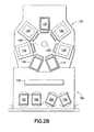
- FIGS. 2A and 2B illustrate a semiconductor tool station incorporating features of the substrate transport apparatus of the present disclosure.
- FIG. 3A is a top perspective view of an embodiment of the present disclosure incorporating an inertial wafer centering end effector with a fork-shaped design.
- FIG. 3B is a top view of an embodiment of the present disclosure incorporating an inertial wafer centering end effector with a fork-shaped design.
- FIG. 4 is a top view of an embodiment of the present disclosure incorporating an inertial wafer centering end effector with a paddle shaped design.
- FIG. 5A is a side view of an embodiment of the inertial wafer centering end effector.
- FIG. 5B is a side view of an embodiment of the inertial wafer centering end effector with a flat work piece present in an eccentric and skewed position after pick.
- FIG. 5C is a side view of an embodiment of the inertial wafer centering end effector with a flat work piece present in a centered and horizontal position after centering.
- FIG. 6A is a side view of another embodiment of the inertial wafer centering end effector.
- FIG. 6B is a side view of another embodiment of the inertial wafer centering end effector with a flat work piece present in the eccentric and skewed position after pick.
- FIG. 6C is a side view of another embodiment of the inertial wafer centering end effector with a flat work piece present in the centered and horizontal position.
- FIG. 7A is a top design view of an end effector blade tip depicting the fiber routing channel for the thru beam sensor.
- FIG. 7B is a side design view of the end effector with a flat work piece and the thru beam sensor beam being interrupted by its presence.
- FIG. 8 is a top perspective view of an end effector support pad and the surfaces for initial flat work piece positioning, centering and capture.
- FIG. 9A is a side view of another embodiment of the inertial wafer centering end effector and transport apparatus.
- FIG. 9B is an enlarged side view of the rear pad portion of FIG. 9A .
- FIG. 9C is an enlarged side view of the front pad portion of FIG. 9A .
- FIG. 10A is a top perspective view of an embodiment of the rear pad assembly of the inertial wafer centering end effector.
- FIG. 10B is a bottom perspective view of an embodiment of the rear pad assembly of the inertial wafer centering end effector.
- FIG. 10C is a top perspective view of an embodiment of the rear pad and rear pad arm of the inertial wafer centering end effector.
- FIG. 11 is another partial top perspective view of the rear pad assembly of the inertial wafer centering end effector.
- the present disclosure relates to a substrate transport apparatus with an end effector for centering and capturing a silicon wafer.
- the end effector and substrate transport apparatus are distinguishable over the prior art in providing and utilizing an inertial capture edge grip with end effector pads that may pick up a substrate in a skewed eccentric position and subsequently center, make horizontal, and capture the flat work piece from inertial movement of the substrate.
- the end effector and substrate transport apparatus disclosed herein offer significant advantages relative to prior art end effectors and transport apparatus. As will be described further below.
- FIG. 1 A substrate transport apparatus 100 incorporating the features of the present disclosure and substrate S are illustrated in FIG. 1 .
- FIG. 1 A substrate transport apparatus 100 incorporating the features of the present disclosure and substrate S are illustrated in FIG. 1 .
- the present disclosure will be described with reference to the exemplary embodiments shown in the drawings, it should be understood that the present disclosure can be embodied in many alternate forms of the embodiments.
- any suitable size, shape or type of elements or materials could be used.
- the transport apparatus 100 is capable of moving a flat work piece or substrate S as desired, such as for example at least along three axes (as indicated by arrows Z, ⁇ , T, in FIG. 1 ).
- the flat work piece is an exemplary work piece and is shown as having a rounded outer circumference for example purposes only.
- the work piece S may be any flat work piece such as 200 mm, 300 mm, 400 mm or any desired size semiconductor wafer used in the manufacture of semiconductor devices, a semiconductor lithography panel such as a mask or reticle, or flat panel displays.
- the transport apparatus 100 has a movable arm 44 that has a general SCARA (selective compliant articulated robot arm) configuration.
- the transport apparatus may have other suitable configuration, with an articulated arm of any suitable type (e.g. frogleg), or with no articulated arm.
- the movable arm 44 in this embodiment is a scara type arm including upper arm 60 , forearm 62 , and end effector 64 .
- any suitable type of transport arm may be used.
- the upper arm 60 and forearm 62 are pivotally linked in series.
- the upper arm 60 is connected to the drive section 42 .
- the drive section 42 of the transport apparatus 100 may be fixedly mounted to a frame (not shown) of a work piece workstation (not shown).
- the drive section 42 may be mounted on a car capable of movement in the horizontal plane relative to the frame of the apparatus.
- the drive section 42 may be a three-axis drive section capable of moving the movable arm 44 along three axes Z, ⁇ , T.
- the drive section 42 may include suitable drive (not shown) for vertically raising and lowering (i.e. movement along the “Z”axis) the movable arm 44 .
- the drive 42 may include a co-axial drive assembly (not shown) for moving the movable arm 44 about the rotation axis ⁇ (i.e. ⁇ movement) and for rotating the upper arm 60 , forearm 62 and end effector 64 to effect extending or retracting the arm along the radial axis T (i.e. T movement).
- coaxial drive assembly A suitable example of a co-axial drive assembly is disclosed in U.S. Pat. No. 5,899,658, which is incorporated by reference herein in its entirety.
- the coaxial drive may be any other suitable drive capable of moving the movable arm to generate both ⁇ movement and T movement.
- Controller 400 is connected to the drive section 42 to control arm movements and the corresponding position of the end effector 64 .
- the end effector 64 is constructed, in this embodiment, for attachment to the end of the forearm 62 and is adapted for supporting the work piece S in a secure manner.
- End effector 64 is constructed having a frame 3 with an attachment 4 and a distal end 5 .
- the work piece is supported from below on support pads (not shown) positioned to contact the work piece S along the circumferential edge 6 .
- the substrate transport apparatus of FIG. 1 may be incorporated into a semiconductor processing tool station 190 in accordance with an exemplary embodiment.
- a semiconductor processing tool is shown in FIG. 2A and 2B
- the substrate transport apparatus disclosed herein may be applied to any tool station or application employing robotic manipulators.
- the tool 190 is shown as a cluster tool, however the exemplary embodiment may be applied to any suitable tool station such as, for example, a linear tool station.
- the tool station 190 generally includes an atmospheric front end 101 , a vacuum load lock 110 and a vacuum back end 120 . In alternate embodiments, the tool station may have any suitable configuration.
- each of the front end 101 , load lock 110 and back end 120 may be connected to a controller which may be part of any suitable control architecture such as, for example, a clustered architecture control.
- the control system may be a closed loop controller having a master controller, cluster controllers and autonomous remote controllers. In alternate embodiments, any suitable controller may be utilized.
- the front end 101 generally includes load port modules 105 and a mini-environment 160 such as for example an equipment front end module (EFEM).
- the load port modules 105 may be box opener/loader to tool standard (BOLTS) interfaces that conform to SEMI standards E15.1, E47.1, E62, E19.5 or E1.9 for 300 mm load ports, front opening or bottom opening boxes/pods and cassettes 150 .
- the load port modules may be configured as 200 mm wafer interfaces or any other suitable substrate interfaces such as for example larger or smaller wafers or flat panels for flat panel displays.
- two load port modules are shown in FIG. 2A , in alternate embodiments, any suitable number of load port modules may be incorporated into the front end 101 .
- the load port modules may be configured to receive substrate carriers or cassettes 150 from an overhead transport system, automated guided vehicles, person guided vehicles, rail guided vehicles or from any other suitable transport method.
- the load port modules 105 may interface with the mini-environment 160 through load ports 140 .
- the load ports 140 may allow the passage of substrates between the substrate cassettes 150 and the mini-environment 160 .
- the mini-environment 160 generally includes a substrate transport apparatus 100 as was described in FIG. 1 .
- the mini-environment 160 may be provided a controlled, clean zone for substrate transfer between multiple load port modules.
- the vacuum load lock 110 may be located between and connected to the mini-environment 160 and the back end 120 .
- the load lock 110 generally includes atmospheric and vacuum slot valves.
- the slot valves may provide the environmental isolation employed to evacuate the load lock after loading a substrate from the atmospheric front end and to maintain the vacuum in the transport chamber when venting the lock with an inert gas such as nitrogen.
- the load lock 110 may also include an aligner 310 for aligning a fiducial of the substrate to a desired position for processing.
- the vacuum load lock may be located in any suitable location of the processing apparatus and have any suitable configuration.
- the vacuum back end 120 generally includes a transport chamber 125 , one or more processing station(s) 130 and a substrate transport apparatus 100 as was described in FIG. 1 .
- the backend substrate transport apparatus 220 may be located within the transport chamber 125 to transport substrates between the load lock 110 and the various processing stations 130 .
- the processing stations may operate on the substrates through various deposition, etching, or other types of processes to form electrical circuitry or other desired structure on the substrates. Non-limiting exemplary processes include etching, chemical vapor deposition (CVD), physical vapor deposition (PVD), ion implantation, metrology, rapid thermal processing (RTP), and dry stripping.
- the processing stations are connected to the transport chamber 125 to allow substrates to be passed from the transport chamber 125 to the processing stations 130 and vice versa.
- one exemplary embodiment of the end effector 64 disclosed herein may have a fork-shaped end effector blade 8 .
- the end effector may be connected to the forearm 62 of the substrate transport apparatus via an attachment 4 .
- the end effector 64 is constructed having a frame 3 with an attachment 4 and a distal end 5 .
- the end effector 64 may have three perimeter pads 22 , 32 a , 32 b attached to the fork-shaped blade 8 for centering and capturing a flat work piece.
- One exemplary flat work piece is a silicon wafer S, also referred to herein as a semiconductor wafer or a substrate.
- the silicon wafer S is supported on the end effector blade by the pads (also referred to herein as support pads) 22 , 32 a , 32 b , which are positioned on the end effector blade 8 to contact the circumferential edge 6 of the wafer S.
- the pads also referred to herein as support pads 22 , 32 a , 32 b
- the edge grip pads may be arranged in any desired configuration.
- the design of the pads 22 , 32 a , 32 b will be described in greater detail below.
- a center point 9 is between the front pads 32 a , 32 b and the rear pad 22 , which represents in the exemplary embodiment a centering position with respect to which the substrate S may be centered by the inertial capture centering grip as will be described below.
- the exemplary embodiment of the end effector 64 also includes a mapping and wafer presence sensor 14 .
- sensor 14 is a thru beam sensor 14 that includes a suitable source 14 a and a suitable source detector 14 b incorporated into the end effector blade tips 12 a , 12 b .
- the thru beam sensor 14 may be used to map silicon wafers S in a carrier or cassette (e.g. carriers 150 see FIGS.
- the mapping and presence sensor may be any suitable type of sensor.
- the inertial wafer centering end effectors disclosed herein may be used with end effector blades having a variety of shapes.
- the end effector may have a paddle-shaped end effector blade 8 is shown.
- the front support pads are attached near the front end of the end effector blade 8 in order to contact the circumferential edge 6 of the wafer S.
- the wafer presence sensor (not shown) may be repositioned and incorporated in the front of the end effector blade 8 for detecting the presence of a wafer S on the end effector 64 .
- a separate mapping sensor (not shown) may be used with the paddle-shaped end effector design [r 1 ].
- the end effector 64 includes an end effector blade 8 with asymmetric front 32 a , 32 b and rear 22 support pads.
- Asymmetric front pads relative to the rear pad means that the two front pads are of a different design than the rear pad.
- the rear pad 22 is positioned towards the attachment end 4 of the end effector 64 and the front pads 32 a , 32 b are positioned towards the distal end 5 of the end effector 64 .
- front and rear are used for convenience to describe the positional reference of the end effector with respect to the travel of the end effector (such as along the axes, T, ⁇ , Z) with the front reaching a given position then the rear when the end effector is advancing (e.g. in the direction indicated by arrow T) and the rear reaching a given position and then the front when returning (e.g. opposite to arrow T).
- a centerline 9 between the two front pads 32 a, 32 b and the one rear pad 22 is also indicated.
- the support surfaces 23 , 33 are defined herein as the surfaces where the circumferential edge 6 of the flat work piece contact the rear and front pads 22 , 32 a , 32 b respectively. In alternate embodiments, the pads may be positioned in any other desired orientation to effect inertial centering and capture.
- FIG. 5A illustrates the front and rear pads without the presence of a flat work piece.
- the two front pads 32 a , 32 b may be similar to each other, having a generally wedge shape with an angle of incidence of ⁇ for the support surfaces 33 a , 33 b of the pads.
- the angle of incidence ⁇ for the front pads 32 a , 32 b may range from about 5 to about 70, or about 20 to about 60, or about 30 to about 50 degrees, though in the exemplary embodiment shown the angle ⁇ is about 8°.
- the angled support surfaces 33 a , 33 b for the two front pads 32 a , 32 b provide a contact and sliding or ramp surface used to contact and support the wafer during initial positioning and then operate to effect capture of the flat work piece or wafer on the end effector 64 .
- the pads may be made from a suitable material, such as PVC or DELRINTM, having suitable lubricious properties to allow substantially free sliding of the peripheral edge of the workpiece over the ramp surface(s) 33 a , 33 b when inertial centering and capture is being effected as described below.
- a carrier, cassette or a processing position e.g.
- the peripheral edge of the wafer, with the wafer in the initial pick position, may rest on the ramp surface.
- the wedge shaped ramp surfaces 33 a , 33 b of the front pads 32 a , 32 b permit the leading edge of the flat work piece to slide and be secured or captured between the pads upon end effector 64 movement.
- the ramp surfaces may also cause centering of the wafer.
- Each of pads 32 a , 32 b may also have a respective buffer surface 35 a , 35 b that operates to stop wafer sliding on the ramp and grip the periphery of the wafer to capture the wafer on the end effector.
- the buffer surface 35 a , 35 b may be oriented substantially vertically or may be inclined or pitched inwards (towards centerline 9 ) in order to trap a portion of the wafer peripheral edge between ramp and buffer surface.
- the height of pads 32 a , 32 b may be sized, so that the profile height of the end effector at the location of pads 32 a , 32 b is less than the SEMI specified spacing between tracked substrates with sufficient clearances to allow free insertion of the end effector between stacked substrates.
- the rear pad 22 may also be wedge shaped, but includes two angled support surfaces 23 a , 23 b with angle of incidences of a and ⁇ respectively (from horizontal reference).
- the angle of incidence of ⁇ is greater than ⁇ .
- the inclined surface 23 b with steeper angle of incidence ⁇ is located closer to the centerline 9 and may range from about 30 to about 80 degrees though in the exemplary embodiment shown, the angle B is about 74°.
- the shallower surface 23 a with angle of incidence ⁇ is located closer to the attachment end 4 and may range from about 10 to about 70 degrees though in the exemplary embodiment shown the angle ⁇ is about 45°.
- the angled support surfaces 23 a , 23 b for the rear pad 22 provide for contact and sliding or ramp surfaces used to initially position, capture, and center the flat work piece on the end effector 64 . More particularly, the rear pad 22 is used to capture and center the trailing edge of the flat work piece when it is picked up by the end effector 64 and substrate transport system 100 from a carrier, cassette, FOUP or a processing position or station (not shown).
- the ramp surface 23 A closer to the attachment end 4 of the rear pad 22 may be sized to accommodate the SEMI specified wafer position range (for a wafer at a wafer station or cassette) as well as any desired eccentricity during the pick (as will be described below) to ensure that for initial positioning, the substrate edge when the substrate is picked up by the end effector 64 will initially rest on ramp 23 A.
- ramp surface 23 A may define the capture range CR of the inertial capture grip.
- the ramp surface 23 A may be located above ramp surface(s) 33 A, 33 B of pads 32 A, 32 B, and as may be realized a substrate with the peripheral edges contacting ramp surfaces 23 A, 33 a 33 b will be pitched with the portion on ramp surface 23 A higher than the portion on ramp surface(s) 33 a , 33 b .
- it may be realized in view of the different angle of inclination ⁇ , respectively of the rear 23 A, and front 33 a , 33 b ramp surfaces (e.g. the rear ramp being more steeply inclined than front ramp) that the rear ramp in the example may be capable of generating an uncompensated force component against the substrate that urges the substrate forwards.
- the support surface 23 B may be used to define the centering range for final positioning of the substrate edge after end effector 64 movement (to be described in greater detail below).
- the front and rear pads 32 a , 32 b , 22 may be positioned with respect to each other so that the captured substrate, having its periphery against buffers 34 a , 35 b , contacts capture surface 23 B of the pad 22 at a location resulting in the substrate being held in a substantially horizontal position held by edge contact only.
- the pads are positioned so that the captured substrate is centered, for example with respect to centering position 9 .
- FIG. 5B illustrates the front and rear pads with a flat work piece S for example at the initial pick from a cassette, carrier, FOUP or a processing position or station (see FIGS. 2A-2B ).
- the flat work piece S for example may be initially picked up in an eccentric position (substrate center SC may be offset from centering position 9 ) between the front and rear pads 32 a , 32 b , 22 .
- the substrate eccentricity for the initial pick may be about 1.0 mm, and sufficient to overcome any positional variance of the substrate at the substrate station. In alternate embodiments, any desired eccentricity may be used.
- the eccentricity e which is in direction towards pad 22 , results in the peripheral edge of the substrate contacting ramp surface 23 A during the initial pick.
- the substrate periphery also rests on ramps 33 a , 33 b and the substrate may be skewed as shown.
- the thru beam sensor (see FIG. 3A ) and controller 200 (see FIG. 2A ) may be used to guide the end effector 64 to pick-up the substrate S in the skewed and eccentric position shown in the example.
- FIG. 5C illustrates the front 32 a , 32 b and rear pads 22 with a flat work piece or substrate S after inertial repositioning of the substrate, such as by movement by the end effector 64 , is used to reposition the substrate S between the support pads 22 , 32 a , 32 b .
- the substrate S may be at static equilibrium but statically due to the geometry of the ramp surfaces 23 A, 33 a, 33 b in the exemplary embodiment on which the substrate S rests.
- the geometry of the ramp surfaces operates in combination with an inertial disturbance of desired magnitude to overcome the static forces, to guide the substrate to the captured as well as centered position.
- an inertial force created by for example acceleration of the end effector 64 effectuates a repositioning of the substrate from the skewed position ( FIG. 5B ) to a horizontal position ( FIG. 5C ), and a centering of the substrate S with respect to the centering reference 9 .
- the end effector may be accelerated in the directions indicated by arrow T, ⁇ in FIG. 1 .
- the end effector may be accelerated in the direction indicated by arrow T′′, which may be aligned with a radial direction of the transport arm.
- the end effector may be accelerated from a substrate pick at a substrate station.
- the inertial effects on substrate S from the end effector acceleration T′′ overcome the static forces (holding the substrate in its skewed position), that result in relative displacement between substrate and pads 22 , 32 a , 32 b in the direction indicated by arrow V′ ( FIG. 5B ) substantially opposite to the motion of the end effector.
- the inertial motion carries the substrate S towards the centered position.
- ramp 23 A generates a biasing force on the substrate S further contributing to the forces (that may include both inertial and direct components) driving the substrate to buffers 34 a, b .
- the lateral inertial force provided by motion of the end effector 64 causes the substrate S to slide down the rear pad surface 23 A with angle of incidence ⁇ , and on to ramp surface 23 B having greater angle of incidence ⁇ of the rear pad 22 .
- the steeper inclination of the ramp surface 23 B further increase the bias force urging the substrate towards buffers 35 a , 35 b and increases the wedging forces on the substrate resulting in capture of the substrate.
- the length of the support surface 23 for the ⁇ angle of incidence defines the centering range CR for final capture of the substrate S after movement of the end effector 64 (see FIG. 5A ).
- the ramp surfaces 33 a , 33 b and buffers 35 a , 35 b on the front pads 32 , 32 b may be arranged to provide centering forces in the X direction (centering forces in the Y direction being provided by inertial effects and ramp surfaces 23 A, 23 B of pad 22 , along with buffers 35 a , 35 b as described above).
- ramp surfaces 33 a , 33 b , and buffers 35 a , 35 b represented by arrow N, normal to the ramp surfaces and buffers, may be positioned angled to the X, Y axes.
- orientations of the ramp surfaces and buffers may be symmetric relative to the Y axis.
- the angled orientation of the ramp surfaces and buffers result in opposing force components along the X axis that tend to center the substrate along the X axis with respect to centering datum 9 .
- eccentricity between substrate and centering datum 9 along the X axis will result in centering force bias generated by ramp surfaces 33 a , 33 b and or buffers 35 a , 35 b against the substrate sliding over the ramp surfaces or buffers, under impetus from inertial effects and/or bias from ramps 23 A, 23 B as it moved to capture driving the substrate to a centered position along the X axis with respect to reference datum 9 .
- the edge of the substrate S slides along on the angle of incidence ⁇ of the support surfaces 33 a , 33 b such as to center the substrate between the front and rear pads 32 a , 32 b , 22 , and reposition it in a horizontal position (along axes X and Y).
- the thru beam sensor (not shown) and controller (not shown) are used to determine if the substrate is centered and in a horizontal position after movement by the end effector 64 .
- the front pads may include two, three, four or more angled ramp surfaces, or a rounded ramp surface with the angle of incidences closer to the centerline generally greater than the angle of incidences further from the centerline in order to provide for a ramp type driving force to capture the substrate between the pads.
- the rear pad may include three, four, five or more angled ramp surfaces, (or rounded ramp surface) with the angle of incidences closer to the centerline generally greater than the angle of incidences further from the centerline in order to provide for a ramp type driving force to both capture and center the substrate between the pads.
- one or more pads may be generally of similar design, whereas one or more pads may be of different design to help establish unstable static and dynamic positions for the substrate biasing the substrate to a captured and/or a centered position.
- the front pads and rear pad may be defined, as previously described, as being asymmetric with respect to one another.
- the number of front pads may be three, four, five or more.
- the number or rear pads may be two, three, four or more.
- controller 200 may be programmed, such as for example during the teaching of the substrate transport apparatus 100 of the substrate pick locations, to position the end effector when picking the substrate in order to generate desired eccentricity between the substrate S and end effector pads 22 , 32 a , 32 b as previously described.
- the locations taught the controller 200 for respectively picking and placing substrates as a given tool location may be different.
- inertial effects in the substrate, to effect capture may be generated from the same transport motion used to transport the substrate to a desired destination without transport movements specific to substrate capture. For example, upon initial pick, withdrawal of the transport to remove the end effector and substrate from the substrate holding location of the tool may effect capture and centering of the substrate on the end effector.
- the two front support pads 132 a , 132 b may each include two angled support surfaces 133 a , 133 b with angle of incidences of ⁇ and ⁇ respectively.
- the one rear pad 122 is wedge-shaped with a single angle of incidence ⁇ .
- Pads 132 a , 132 b may be similar to pad 22 described previously and pad 122 may be similar to pads 32 a , 32 b . Similar features are similarly numbered. Referring to FIG.
- the two front pads may each include two angled support surfaces 133 a , 133 b with angle of incidences of ⁇ and ⁇ respectively.
- the angle of incidence of ⁇ is greater than ⁇ .
- the steeper angle of incidence ⁇ is located closer to the centerline 9 .
- the shallower angle of incidence ⁇ is located closer to the distal end 5 .
- the angled support surfaces 133 a , 133 b for the two front pads 132 a , 132 b provide for contact and sliding surfaces used to initially position, and then capture and center the flat work piece on the end effector 64 .
- the rear pad 122 may be wedge shaped with a single angle of incidence ⁇ for the ramp surface 123 .
- FIG. 6B illustrates the front and rear pads with a flat work piece S after initial pick from a cassette, carrier, FOUP or a processing position or station (not shown).
- the flat work piece S is initially picked up in a skewed and eccentric position between the front and rear pads 132 a , 132 b , 122 .
- FIG. 6C illustrates the front and rear pads with a flat work piece S after movement by the end effector 64 is used to reposition the substrate S between the support pads 122 , 132 a , 132 b in a manner similar to that previously described.
- the lateral force provided by acceleration of the end effector 64 causes the substrate S to slide down the two front pad surfaces 133 a , 133 b from angle of incidence ⁇ to angle of incidence ⁇ of the front pads 132 a , 132 b .
- the length of the support surfaces 133 a , 133 b for the ⁇ angle of incidence defines the centering range for final capture of the substrate S after movement of the end effector 64 .
- the edge of the substrate S slides along on the angle of incidence ⁇ of the support surface 23 such as to center the substrate between the front and rear pads 32 a , 32 b , 22 , and reposition it in a horizontal position.
- the thru beam sensor (not shown) and controller (not shown) are used to determine if the substrate is centered and in a horizontal position after movement by the end effector 64 .
- FIG. 7A illustrates a lower surface of a representative pad 32 showing an example of a fiber routing channel for a fork-shaped end effector blade tip 12 .
- the fiber routing channel 15 is positioned within the end effector blade 8 and travels out to the end effector blade tip 12 where the thru beam sensor 14 may be located adjacent to the inside surface 16 of the blade tip 12 .
- the front support pads 32 a , 32 b may be attached to the end effector blade tip 12 . This positioning of the thru beam sensor 14 permits it to be used for mapping substrates within carriers, cassettes and processing stations, and also for detecting the presence and proper positioning of substrates (see FIGS. 5C, 6C ) on the support pads.
- FIG. 7B is a side design view of a portion of the fork-shaped end effector disclosed herein with a flat work piece S supported by a front support pad 32 (similar to pads 32 a , 32 b described previously).
- the front support pad 32 is attached to the fork-shaped end effector blade 8 at the blade tip 12 .
- FIG. 7B illustrates the location of the thru beam generated by (suitable source of) sensor 14 position so as to detect the presence of the flat work piece S on the wedge-shaped front support pad 32 .
- the thru beam sensor source 14 is fully interrupted by the flat work piece S is indicative that the flat work piece S is correctly positioned on the end effector.
- the sensor may be connected to the controller to send a signal upon detection that the substrate S is located in the desired position and hence captured and centered.
- the controller may also be programmed to register lack of a wafer presence signal from the sensor, in response to which the controller may access suitable program to bring the transport to a stop with a motion profile ensuring the wafer is not lost.
- the controller may for example initiate a fault signal, and after stop may retry a substrate capture motion (in the event the substrate did not fully seat before) or may initiate some other desired recovery program.
- FIG. 8 is a top perspective view of a representative rear support pad 22 in accordance with an exemplary embodiment.
- the pad may have mounting holes 24 , 26 (two are shown for example) for securing it to the end effector blade 8 and the two radial or angled support surfaces 23 A, 23 B for inertial work piece positioning, and work piece centering and capture.
- FIG. 8B bolts, screws or other suitable fastening means (not shown) may be used to attach the support pad 22 to the end effector blade 8 .
- the substrate transport apparatus may include a plurality of end effectors in substantially position relative to one another.
- Non-limiting examples include a substrate transport apparatus with two, three, four, five, or more inertial wafer centering end effectors disposed in a parallel position relative to each other.
- a plurality of end effectors on a given transport apparatus permits for two or more flat work pieces to be simultaneously picked up, positioned, centered, captured and transported.
- FIG. 9A illustrates an exemplary substrate transport system 200 with two end effectors 164 attached to corresponding forearms 162 connected to a drive section 142 .
- the two parallel end effectors 164 may be similar to each other, and to end effector 64 described before (each have an end effector blade 108 on which the two front pads 132 a , 132 b and one rear pad 122 may be attached) similar features are similarly numbered.
- the end effector blades may be of the same or a different shape (fork-shaped, paddle-shaped or other).
- the height of each parallel end effector 162 including the attached front and rear support pads 132 a , 132 b , 122 is such it may fit between closely spaced silicon wafers (not shown) stored within a cassette.
- FIG. 9B is an exemplary side design view of the two parallel rear pads 122 .
- the two parallel rear pads 122 each have two angled or profiled support surfaces 123 for substrate (not shown) initial positioning, centering and capture.
- FIG. 10A a schematic of an exemplary embodiment of the rear pad assembly 30 of the inertial wafer centering end effector disclosed herein illustrates that it may be slotted for front to rear adjustability. This permits the rear pad 22 position to be easily altered relative to the distal end of the end effector blade 8 to accommodate different size flat work pieces. Also depicted is the attachment 4 which connects the end effector 64 to the forearm 62 .
- FIG. 10B is a bottom view of the rear pad assembly 30 and illustrates that in the exemplary embodiment the rear pad (see FIG. 10A ) may be mounted to a rear pad arm 27 via suitable fasteners such as bolts or screws 24 A, 26 A.
- the rear pad arm 27 may also be attached to the attachment 4 via bolts or screws 28 , 29 .
- the rear pad assembly 30 including the rear pad arm 27 and the rear pad 22 is also illustrated in FIG. 10C .
- the rear pad assembly 30 may be easily removed from the end effector 64 when desired such as for repair or replacement of the rear pad 22 .
- the rear pad assembly 30 in accordance with another exemplary embodiment may be mounted as a spring loaded type mechanism 31 to allow for further flexibility in front to rear adjustability of the rear pad 22 relative to the end effector blade 8 .
- the rear pad assembly 30 including the rear pad and the rear pad arm 27 may also be fabricated to move along the attachment 4 between the forearm 62 and end effector 64 via a pin and slot type mechanism 35 to further facilitate front to rear adjustability of the rear support pad 22 .
- One or more pins 36 are located in the attachment plate 4 and one or more slots 37 are located in the rear pad arm 27 .
- This pin and slot type mechanism (also referred to as a sliding tongue type mechanism) 35 allows for the rear support pad to be quickly adjusted from front to rear of the end effector blade to accommodate for changes in flat work piece diameter and rear pad 22 dimensions due to surface wear.
- an advantageous method for transporting a flat work piece includes initially providing a flat work piece transport apparatus including a drive shaft, a movable arm connected to the drive shaft, an end effector connected to the moveable arm, wherein the end effector includes asymmetric front and rear pads mounted to the end effector blade and a thru beam sensor mounted within the end effector blade, and a controller for coordinating the drive section, the moveable arm, the end effector and the thru beam sensor.
- the thru beam sensor is used to map the position of the flat work piece relative to the position of the front and rear pads of the end effector blade.
- the thru beam sensor may then be used to detect an eccentricity of the flat work piece on the support surfaces of the front and rear pad.
- the end effector may be moved to provide a lateral force to the flat work piece to simultaneously center and capture the flat work piece in between the front and rear pads in a horizontal position as is depicted in FIGS. 5C and 6C .
- the centered and captured flat work piece may then be transported to one or more processing stations, and in particular stations for silicon wafer processing.
- Non-limiting exemplary processing stations include etching, chemical vapor deposition, physical vapor deposition, ion implantation, metrology, rapid thermal processing, dry stripping and combinations thereof.
Abstract
Description
Claims (22)
Priority Applications (5)
| Application Number | Priority Date | Filing Date | Title |
|---|---|---|---|
| US11/741,416 US9437469B2 (en) | 2007-04-27 | 2007-04-27 | Inertial wafer centering end effector and transport apparatus |
| PCT/US2008/005438 WO2008134041A1 (en) | 2007-04-27 | 2008-04-28 | Inertial wafer centering and effector and transport apparatus |
| KR1020097024587A KR101475790B1 (en) | 2007-04-27 | 2008-04-28 | Inertial wafer centering end effector and transport apparatus |
| JP2010506290A JP2010525608A (en) | 2007-04-27 | 2008-04-28 | Inertial wafer centering end effector and transfer device |
| TW097115511A TWI527149B (en) | 2007-04-27 | 2008-04-28 | Inertial wafer centering end effector and transport apparatus |
Applications Claiming Priority (1)
| Application Number | Priority Date | Filing Date | Title |
|---|---|---|---|
| US11/741,416 US9437469B2 (en) | 2007-04-27 | 2007-04-27 | Inertial wafer centering end effector and transport apparatus |
Publications (2)
| Publication Number | Publication Date |
|---|---|
| US20080267747A1 US20080267747A1 (en) | 2008-10-30 |
| US9437469B2 true US9437469B2 (en) | 2016-09-06 |
Family
ID=39887178
Family Applications (1)
| Application Number | Title | Priority Date | Filing Date |
|---|---|---|---|
| US11/741,416 Active 2031-04-21 US9437469B2 (en) | 2007-04-27 | 2007-04-27 | Inertial wafer centering end effector and transport apparatus |
Country Status (5)
| Country | Link |
|---|---|
| US (1) | US9437469B2 (en) |
| JP (1) | JP2010525608A (en) |
| KR (1) | KR101475790B1 (en) |
| TW (1) | TWI527149B (en) |
| WO (1) | WO2008134041A1 (en) |
Cited By (3)
| Publication number | Priority date | Publication date | Assignee | Title |
|---|---|---|---|---|
| US10649599B2 (en) | 2017-06-30 | 2020-05-12 | Samsung Electronics Co., Ltd. | Electronic device for detecting proximity of user and operation method thereof |
| US11103126B2 (en) * | 2017-05-03 | 2021-08-31 | Lsi Solutions, Inc. | Surgical equipment holder |
| US11864958B2 (en) | 2017-05-03 | 2024-01-09 | Lsi Solutions, Inc. | Surgical equipment holder |
Families Citing this family (23)
| Publication number | Priority date | Publication date | Assignee | Title |
|---|---|---|---|---|
| JP4313824B2 (en) * | 2007-03-23 | 2009-08-12 | 東京エレクトロン株式会社 | Substrate transfer apparatus, substrate transfer method, and storage medium |
| US8430226B2 (en) * | 2008-03-05 | 2013-04-30 | Hirata Corporation | Work transfer apparatus |
| KR20110002483A (en) * | 2008-05-28 | 2011-01-07 | 히라따기꼬오 가부시키가이샤 | Production device |
| TWI614831B (en) * | 2011-03-11 | 2018-02-11 | 布魯克斯自動機械公司 | Substrate processing tool |
| JP5940342B2 (en) * | 2011-07-15 | 2016-06-29 | 東京エレクトロン株式会社 | Substrate transport apparatus, substrate processing system, substrate transport method, and storage medium |
| JP5859236B2 (en) * | 2011-07-15 | 2016-02-10 | ファスフォードテクノロジ株式会社 | Frame supply apparatus and frame supply method |
| US9431282B2 (en) * | 2011-12-27 | 2016-08-30 | Rudolph Technologies, Inc. | Wafer inversion mechanism |
| TWI456685B (en) * | 2012-05-02 | 2014-10-11 | Advanced Wireless Semiconductor Company | Wafer transmission device of etching equipment for concentrated photovoltaics |
| TWI625814B (en) * | 2012-07-27 | 2018-06-01 | 荏原製作所股份有限公司 | Workpiece transport device |
| JP5425998B2 (en) * | 2012-11-13 | 2014-02-26 | 東京エレクトロン株式会社 | Substrate holding member, substrate transfer arm, and substrate transfer device |
| KR101416591B1 (en) * | 2012-12-20 | 2014-07-08 | 주식회사 선익시스템 | Device for transferring board by hand |
| DE102013208301A1 (en) * | 2013-05-06 | 2014-10-16 | Siltronic Ag | Arrangement comprising a semiconductor wafer and a step-shaped support for supporting the semiconductor wafer |
| JP5750472B2 (en) * | 2013-05-22 | 2015-07-22 | 株式会社安川電機 | Substrate transport robot, substrate transport system, and method for detecting substrate arrangement state |
| CN103700612B (en) * | 2013-12-02 | 2016-06-29 | 合肥京东方光电科技有限公司 | A kind of end effector component |
| JP6313972B2 (en) * | 2013-12-26 | 2018-04-18 | 川崎重工業株式会社 | End effector and substrate transfer robot |
| US9991152B2 (en) | 2014-03-06 | 2018-06-05 | Cascade Microtech, Inc. | Wafer-handling end effectors with wafer-contacting surfaces and sealing structures |
| US9425076B2 (en) * | 2014-07-03 | 2016-08-23 | Applied Materials, Inc. | Substrate transfer robot end effector |
| US9779977B2 (en) | 2015-04-15 | 2017-10-03 | Lam Research Corporation | End effector assembly for clean/dirty substrate handling |
| KR102587203B1 (en) * | 2015-07-13 | 2023-10-10 | 브룩스 오토메이션 인코퍼레이티드 | On-the-fly automatic wafer centering method and device |
| WO2017106263A1 (en) | 2015-12-16 | 2017-06-22 | Comau Llc | Adaptable end effector and method |
| USD822735S1 (en) * | 2017-03-17 | 2018-07-10 | Donald Dimattia, Jr. | Positionable end effector link |
| US20190013215A1 (en) * | 2017-07-05 | 2019-01-10 | Kawasaki Jukogyo Kabushiki Kaisha | Substrate holding hand and substrate conveying apparatus including the same |
| CN111958615A (en) * | 2020-08-19 | 2020-11-20 | 西安奕斯伟硅片技术有限公司 | Assembly and method for conveying wafer |
Citations (15)
| Publication number | Priority date | Publication date | Assignee | Title |
|---|---|---|---|---|
| US5669644A (en) | 1995-11-13 | 1997-09-23 | Kokusai Electric Co., Ltd. | Wafer transfer plate |
| JPH11330198A (en) | 1998-05-15 | 1999-11-30 | Tokyo Electron Ltd | Substrate carrying equipment and substrate processing equipment |
| JP2000252347A (en) | 1999-03-01 | 2000-09-14 | Kawasaki Heavy Ind Ltd | Method and apparatus for conveyance of substrate as well as substrate conveyance arm |
| US6520726B1 (en) | 1999-03-03 | 2003-02-18 | Pri Automation, Inc. | Apparatus and method for using a robot to remove a substrate carrier door |
| US20030035711A1 (en) * | 2001-07-14 | 2003-02-20 | Ulysses Gilchrist | Centering double side edge grip end effector with integrated mapping sensor |
| US20030085582A1 (en) * | 2001-07-13 | 2003-05-08 | Woodruff Daniel J. | End-effectors for handling microelectronic workpieces |
| US6678581B2 (en) | 2002-01-14 | 2004-01-13 | Taiwan Semiconductor Manufacturing Co. Ltd | Method of calibrating a wafer edge gripping end effector |
| JP2004273847A (en) | 2003-03-10 | 2004-09-30 | Tokyo Electron Ltd | Substrate carrying apparatus |
| US20040258514A1 (en) | 2002-06-12 | 2004-12-23 | Ivo Raaijmakers | Semiconductor wafer position shift measurement and correction |
| US20050265814A1 (en) | 2003-09-10 | 2005-12-01 | Coady Matthew W | Substrate handling system for aligning and orienting substrates during a transfer operation |
| US7048316B1 (en) * | 2002-07-12 | 2006-05-23 | Novellus Systems, Inc. | Compound angled pad end-effector |
| US20060222480A1 (en) | 2005-03-30 | 2006-10-05 | Duhamel Michael A | Substrate transport apparatus with active edge gripper |
| US20070128008A1 (en) * | 2005-12-06 | 2007-06-07 | Tokyo Electron Limited | Substrate transfer method and substrate transfer apparatus |
| US7233842B2 (en) * | 1998-12-02 | 2007-06-19 | Brooks Automation, Inc. | Method of determining axial alignment of the centroid of an edge gripping end effector and the center of a specimen gripped by it |
| JP2008235810A (en) | 2007-03-23 | 2008-10-02 | Tokyo Electron Ltd | Heat treatment method, heat treatment device, and method for transferring substrate to be treated |
Family Cites Families (5)
| Publication number | Priority date | Publication date | Assignee | Title |
|---|---|---|---|---|
| JPH07153818A (en) * | 1993-11-30 | 1995-06-16 | Daihen Corp | Semiconductor wafer recognition equipment |
| JPH10308436A (en) * | 1997-05-08 | 1998-11-17 | Olympus Optical Co Ltd | Substrate carrying device |
| JP2000124289A (en) * | 1998-10-19 | 2000-04-28 | Mecs Corp | Hand of thin substrate transfer robot |
| EP1313662B1 (en) * | 1999-05-04 | 2014-03-26 | Ade Corporation | Edge gripping end effector wafer handling apparatus |
| JP4258964B2 (en) * | 2000-09-26 | 2009-04-30 | 神鋼電機株式会社 | Wafer transfer equipment |
-
2007
- 2007-04-27 US US11/741,416 patent/US9437469B2/en active Active
-
2008
- 2008-04-28 JP JP2010506290A patent/JP2010525608A/en active Pending
- 2008-04-28 TW TW097115511A patent/TWI527149B/en active
- 2008-04-28 WO PCT/US2008/005438 patent/WO2008134041A1/en active Application Filing
- 2008-04-28 KR KR1020097024587A patent/KR101475790B1/en active IP Right Grant
Patent Citations (16)
| Publication number | Priority date | Publication date | Assignee | Title |
|---|---|---|---|---|
| US5669644A (en) | 1995-11-13 | 1997-09-23 | Kokusai Electric Co., Ltd. | Wafer transfer plate |
| JPH11330198A (en) | 1998-05-15 | 1999-11-30 | Tokyo Electron Ltd | Substrate carrying equipment and substrate processing equipment |
| US7233842B2 (en) * | 1998-12-02 | 2007-06-19 | Brooks Automation, Inc. | Method of determining axial alignment of the centroid of an edge gripping end effector and the center of a specimen gripped by it |
| JP2000252347A (en) | 1999-03-01 | 2000-09-14 | Kawasaki Heavy Ind Ltd | Method and apparatus for conveyance of substrate as well as substrate conveyance arm |
| US6520726B1 (en) | 1999-03-03 | 2003-02-18 | Pri Automation, Inc. | Apparatus and method for using a robot to remove a substrate carrier door |
| US20030085582A1 (en) * | 2001-07-13 | 2003-05-08 | Woodruff Daniel J. | End-effectors for handling microelectronic workpieces |
| JP2004535681A (en) | 2001-07-14 | 2004-11-25 | ブルックス オートメーション インコーポレイテッド | Centered bilateral edge grip end effector with integrated mapping sensor |
| US20030035711A1 (en) * | 2001-07-14 | 2003-02-20 | Ulysses Gilchrist | Centering double side edge grip end effector with integrated mapping sensor |
| US6678581B2 (en) | 2002-01-14 | 2004-01-13 | Taiwan Semiconductor Manufacturing Co. Ltd | Method of calibrating a wafer edge gripping end effector |
| US20040258514A1 (en) | 2002-06-12 | 2004-12-23 | Ivo Raaijmakers | Semiconductor wafer position shift measurement and correction |
| US7048316B1 (en) * | 2002-07-12 | 2006-05-23 | Novellus Systems, Inc. | Compound angled pad end-effector |
| JP2004273847A (en) | 2003-03-10 | 2004-09-30 | Tokyo Electron Ltd | Substrate carrying apparatus |
| US20050265814A1 (en) | 2003-09-10 | 2005-12-01 | Coady Matthew W | Substrate handling system for aligning and orienting substrates during a transfer operation |
| US20060222480A1 (en) | 2005-03-30 | 2006-10-05 | Duhamel Michael A | Substrate transport apparatus with active edge gripper |
| US20070128008A1 (en) * | 2005-12-06 | 2007-06-07 | Tokyo Electron Limited | Substrate transfer method and substrate transfer apparatus |
| JP2008235810A (en) | 2007-03-23 | 2008-10-02 | Tokyo Electron Ltd | Heat treatment method, heat treatment device, and method for transferring substrate to be treated |
Cited By (3)
| Publication number | Priority date | Publication date | Assignee | Title |
|---|---|---|---|---|
| US11103126B2 (en) * | 2017-05-03 | 2021-08-31 | Lsi Solutions, Inc. | Surgical equipment holder |
| US11864958B2 (en) | 2017-05-03 | 2024-01-09 | Lsi Solutions, Inc. | Surgical equipment holder |
| US10649599B2 (en) | 2017-06-30 | 2020-05-12 | Samsung Electronics Co., Ltd. | Electronic device for detecting proximity of user and operation method thereof |
Also Published As
| Publication number | Publication date |
|---|---|
| TWI527149B (en) | 2016-03-21 |
| US20080267747A1 (en) | 2008-10-30 |
| WO2008134041A1 (en) | 2008-11-06 |
| JP2010525608A (en) | 2010-07-22 |
| TW200908195A (en) | 2009-02-16 |
| KR101475790B1 (en) | 2014-12-23 |
| KR20100023821A (en) | 2010-03-04 |
Similar Documents
| Publication | Publication Date | Title |
|---|---|---|
| US9437469B2 (en) | Inertial wafer centering end effector and transport apparatus | |
| US20200388523A1 (en) | Wafer aligner | |
| US11420337B2 (en) | Transport apparatus | |
| US11664259B2 (en) | Process apparatus with on-the-fly substrate centering | |
| TWI710440B (en) | Tool auto-teach method and apparatus | |
| US9728436B2 (en) | Transfer mechanism with multiple wafer handling capability | |
| US10607879B2 (en) | Substrate processing apparatus | |
| US20130216336A1 (en) | Automatic carrier transfer for transferring a substrate carrier in a semiconductor manufacturing post-process and method of transferring the substrate carrier using the same | |
| US20090092470A1 (en) | End effector with sensing capabilities | |
| US20140314535A1 (en) | Substrate handler |
Legal Events
| Date | Code | Title | Description |
|---|---|---|---|
| AS | Assignment |
Owner name: BROOKS AUTOMATION, INC., MASSACHUSETTS Free format text: ASSIGNMENT OF ASSIGNORS INTEREST;ASSIGNOR:FOSNIGHT, WILLIAM;REEL/FRAME:019957/0024 Effective date: 20070815 |
|
| AS | Assignment |
Owner name: WELLS FARGO BANK, NATIONAL ASSOCIATION, MASSACHUSETTS Free format text: SECURITY AGREEMENT;ASSIGNORS:BROOKS AUTOMATION, INC.;BIOSTORAGE TECHNOLOGIES;REEL/FRAME:038891/0765 Effective date: 20160526 Owner name: WELLS FARGO BANK, NATIONAL ASSOCIATION, MASSACHUSE Free format text: SECURITY AGREEMENT;ASSIGNORS:BROOKS AUTOMATION, INC.;BIOSTORAGE TECHNOLOGIES;REEL/FRAME:038891/0765 Effective date: 20160526 |
|
| STCF | Information on status: patent grant |
Free format text: PATENTED CASE |
|
| AS | Assignment |
Owner name: MORGAN STANLEY SENIOR FUNDING, INC., MARYLAND Free format text: SECURITY INTEREST;ASSIGNORS:BROOKS AUTOMATION, INC.;BIOSTORAGE TECHNOLOGIES, INC.;REEL/FRAME:044142/0258 Effective date: 20171004 |
|
| MAFP | Maintenance fee payment |
Free format text: PAYMENT OF MAINTENANCE FEE, 4TH YEAR, LARGE ENTITY (ORIGINAL EVENT CODE: M1551); ENTITY STATUS OF PATENT OWNER: LARGE ENTITY Year of fee payment: 4 |
|
| AS | Assignment |
Owner name: BROOKS AUTOMATION US, LLC, MASSACHUSETTS Free format text: ASSIGNMENT OF ASSIGNORS INTEREST;ASSIGNOR:BROOKS AUTOMATION HOLDING, LLC;REEL/FRAME:058482/0001 Effective date: 20211001 Owner name: BROOKS AUTOMATION HOLDING, LLC, MASSACHUSETTS Free format text: ASSIGNMENT OF ASSIGNORS INTEREST;ASSIGNOR:BROOKS AUTOMATION,INC;REEL/FRAME:058481/0740 Effective date: 20211001 |
|
| AS | Assignment |
Owner name: GOLDMAN SACHS BANK USA, NEW YORK Free format text: SECOND LIEN PATENT SECURITY AGREEMENT;ASSIGNOR:BROOKS AUTOMATION US, LLC;REEL/FRAME:058945/0748 Effective date: 20220201 Owner name: BARCLAYS BANK PLC, UNITED KINGDOM Free format text: FIRST LIEN PATENT SECURITY AGREEMENT;ASSIGNOR:BROOKS AUTOMATION US, LLC;REEL/FRAME:058950/0146 Effective date: 20220201 |
|
| MAFP | Maintenance fee payment |
Free format text: PAYMENT OF MAINTENANCE FEE, 8TH YEAR, LARGE ENTITY (ORIGINAL EVENT CODE: M1552); ENTITY STATUS OF PATENT OWNER: LARGE ENTITY Year of fee payment: 8 |