US9419189B1 - Small LED source with high brightness and high efficiency - Google Patents
Small LED source with high brightness and high efficiency Download PDFInfo
- Publication number
- US9419189B1 US9419189B1 US14/528,818 US201414528818A US9419189B1 US 9419189 B1 US9419189 B1 US 9419189B1 US 201414528818 A US201414528818 A US 201414528818A US 9419189 B1 US9419189 B1 US 9419189B1
- Authority
- US
- United States
- Prior art keywords
- led
- lighting system
- light
- submount
- color
- Prior art date
- Legal status (The legal status is an assumption and is not a legal conclusion. Google has not performed a legal analysis and makes no representation as to the accuracy of the status listed.)
- Active
Links
- 239000000463 material Substances 0.000 claims description 131
- 238000006243 chemical reaction Methods 0.000 claims description 61
- 238000002310 reflectometry Methods 0.000 claims description 32
- 239000000758 substrate Substances 0.000 claims description 6
- 239000007769 metal material Substances 0.000 claims description 2
- 150000001875 compounds Chemical class 0.000 claims 1
- 238000000034 method Methods 0.000 abstract description 12
- 238000013461 design Methods 0.000 description 34
- 239000004065 semiconductor Substances 0.000 description 18
- 230000003287 optical effect Effects 0.000 description 17
- 238000004519 manufacturing process Methods 0.000 description 14
- 230000006870 function Effects 0.000 description 12
- 229910052751 metal Inorganic materials 0.000 description 12
- 239000002184 metal Substances 0.000 description 12
- 239000000919 ceramic Substances 0.000 description 8
- 229910052736 halogen Inorganic materials 0.000 description 8
- 229910052712 strontium Inorganic materials 0.000 description 8
- GWEVSGVZZGPLCZ-UHFFFAOYSA-N Titan oxide Chemical compound O=[Ti]=O GWEVSGVZZGPLCZ-UHFFFAOYSA-N 0.000 description 7
- 238000013459 approach Methods 0.000 description 7
- 229910052791 calcium Inorganic materials 0.000 description 7
- 150000002367 halogens Chemical class 0.000 description 7
- 239000002105 nanoparticle Substances 0.000 description 7
- -1 polyethylene Polymers 0.000 description 7
- OAICVXFJPJFONN-UHFFFAOYSA-N Phosphorus Chemical compound [P] OAICVXFJPJFONN-UHFFFAOYSA-N 0.000 description 6
- 239000002245 particle Substances 0.000 description 6
- 239000002096 quantum dot Substances 0.000 description 6
- 238000004891 communication Methods 0.000 description 5
- 230000003247 decreasing effect Effects 0.000 description 5
- 230000000694 effects Effects 0.000 description 5
- 238000000295 emission spectrum Methods 0.000 description 5
- 238000003384 imaging method Methods 0.000 description 5
- 238000002156 mixing Methods 0.000 description 5
- 239000000203 mixture Substances 0.000 description 5
- 150000004767 nitrides Chemical class 0.000 description 5
- 239000010409 thin film Substances 0.000 description 5
- 229910052788 barium Inorganic materials 0.000 description 4
- 230000007423 decrease Effects 0.000 description 4
- 238000010586 diagram Methods 0.000 description 4
- 150000002500 ions Chemical class 0.000 description 4
- 239000011148 porous material Substances 0.000 description 4
- 239000012780 transparent material Substances 0.000 description 4
- JMASRVWKEDWRBT-UHFFFAOYSA-N Gallium nitride Chemical compound [Ga]#N JMASRVWKEDWRBT-UHFFFAOYSA-N 0.000 description 3
- 150000001768 cations Chemical class 0.000 description 3
- 230000008878 coupling Effects 0.000 description 3
- 238000010168 coupling process Methods 0.000 description 3
- 238000005859 coupling reaction Methods 0.000 description 3
- 239000002019 doping agent Substances 0.000 description 3
- 239000008393 encapsulating agent Substances 0.000 description 3
- 239000010408 film Substances 0.000 description 3
- 229920001296 polysiloxane Polymers 0.000 description 3
- 230000009467 reduction Effects 0.000 description 3
- VYPSYNLAJGMNEJ-UHFFFAOYSA-N silicon dioxide Inorganic materials O=[Si]=O VYPSYNLAJGMNEJ-UHFFFAOYSA-N 0.000 description 3
- OKTJSMMVPCPJKN-UHFFFAOYSA-N Carbon Chemical compound [C] OKTJSMMVPCPJKN-UHFFFAOYSA-N 0.000 description 2
- 229910052688 Gadolinium Inorganic materials 0.000 description 2
- 229910019142 PO4 Inorganic materials 0.000 description 2
- BQCADISMDOOEFD-UHFFFAOYSA-N Silver Chemical compound [Ag] BQCADISMDOOEFD-UHFFFAOYSA-N 0.000 description 2
- 229910052771 Terbium Inorganic materials 0.000 description 2
- 230000000903 blocking effect Effects 0.000 description 2
- 230000001413 cellular effect Effects 0.000 description 2
- 150000004770 chalcogenides Chemical class 0.000 description 2
- 239000002131 composite material Substances 0.000 description 2
- 230000002939 deleterious effect Effects 0.000 description 2
- 239000003989 dielectric material Substances 0.000 description 2
- 238000005516 engineering process Methods 0.000 description 2
- 229910052733 gallium Inorganic materials 0.000 description 2
- 229910052732 germanium Inorganic materials 0.000 description 2
- 229910052735 hafnium Inorganic materials 0.000 description 2
- 238000005286 illumination Methods 0.000 description 2
- 238000002347 injection Methods 0.000 description 2
- 239000007924 injection Substances 0.000 description 2
- 239000004973 liquid crystal related substance Substances 0.000 description 2
- 229910001507 metal halide Inorganic materials 0.000 description 2
- 150000005309 metal halides Chemical class 0.000 description 2
- 229910052594 sapphire Inorganic materials 0.000 description 2
- 239000010980 sapphire Substances 0.000 description 2
- 239000000377 silicon dioxide Substances 0.000 description 2
- 239000000126 substance Substances 0.000 description 2
- 229910052718 tin Inorganic materials 0.000 description 2
- 229910052719 titanium Inorganic materials 0.000 description 2
- 239000010936 titanium Substances 0.000 description 2
- OGIDPMRJRNCKJF-UHFFFAOYSA-N titanium oxide Inorganic materials [Ti]=O OGIDPMRJRNCKJF-UHFFFAOYSA-N 0.000 description 2
- 229910052725 zinc Inorganic materials 0.000 description 2
- 229910052726 zirconium Inorganic materials 0.000 description 2
- 239000004593 Epoxy Substances 0.000 description 1
- 229910017414 LaAl Inorganic materials 0.000 description 1
- HBBGRARXTFLTSG-UHFFFAOYSA-N Lithium ion Chemical compound [Li+] HBBGRARXTFLTSG-UHFFFAOYSA-N 0.000 description 1
- 229910052765 Lutetium Inorganic materials 0.000 description 1
- 229910017623 MgSi2 Inorganic materials 0.000 description 1
- 239000004698 Polyethylene Substances 0.000 description 1
- 229910003564 SiAlON Inorganic materials 0.000 description 1
- 241000314701 Toxolasma parvus Species 0.000 description 1
- 239000012190 activator Substances 0.000 description 1
- 150000004645 aluminates Chemical class 0.000 description 1
- 150000001450 anions Chemical class 0.000 description 1
- 230000008901 benefit Effects 0.000 description 1
- 230000005540 biological transmission Effects 0.000 description 1
- 229910052792 caesium Inorganic materials 0.000 description 1
- 238000003486 chemical etching Methods 0.000 description 1
- 239000011248 coating agent Substances 0.000 description 1
- 238000000576 coating method Methods 0.000 description 1
- 229910052681 coesite Inorganic materials 0.000 description 1
- 210000001072 colon Anatomy 0.000 description 1
- 239000003086 colorant Substances 0.000 description 1
- 239000000470 constituent Substances 0.000 description 1
- 238000010276 construction Methods 0.000 description 1
- 229910052906 cristobalite Inorganic materials 0.000 description 1
- 239000013078 crystal Substances 0.000 description 1
- 230000001419 dependent effect Effects 0.000 description 1
- 230000008021 deposition Effects 0.000 description 1
- 238000009826 distribution Methods 0.000 description 1
- 238000001312 dry etching Methods 0.000 description 1
- 239000000835 fiber Substances 0.000 description 1
- 150000002222 fluorine compounds Chemical class 0.000 description 1
- 238000009472 formulation Methods 0.000 description 1
- 238000010438 heat treatment Methods 0.000 description 1
- 229910052909 inorganic silicate Inorganic materials 0.000 description 1
- 239000007788 liquid Substances 0.000 description 1
- 229910001416 lithium ion Inorganic materials 0.000 description 1
- 238000004020 luminiscence type Methods 0.000 description 1
- 229910052749 magnesium Inorganic materials 0.000 description 1
- 239000011159 matrix material Substances 0.000 description 1
- 238000012986 modification Methods 0.000 description 1
- 230000004048 modification Effects 0.000 description 1
- 238000001579 optical reflectometry Methods 0.000 description 1
- 239000012071 phase Substances 0.000 description 1
- 235000021317 phosphate Nutrition 0.000 description 1
- 150000003013 phosphoric acid derivatives Chemical class 0.000 description 1
- 239000004033 plastic Substances 0.000 description 1
- 229920003023 plastic Polymers 0.000 description 1
- 229920000573 polyethylene Polymers 0.000 description 1
- 229920001343 polytetrafluoroethylene Polymers 0.000 description 1
- 239000004810 polytetrafluoroethylene Substances 0.000 description 1
- 229910052700 potassium Inorganic materials 0.000 description 1
- 238000012545 processing Methods 0.000 description 1
- 230000004044 response Effects 0.000 description 1
- 210000001525 retina Anatomy 0.000 description 1
- 229910052701 rubidium Inorganic materials 0.000 description 1
- 238000012163 sequencing technique Methods 0.000 description 1
- 150000004760 silicates Chemical class 0.000 description 1
- 229910052709 silver Inorganic materials 0.000 description 1
- 239000004332 silver Substances 0.000 description 1
- 239000007787 solid Substances 0.000 description 1
- 239000007790 solid phase Substances 0.000 description 1
- 238000001228 spectrum Methods 0.000 description 1
- 230000007480 spreading Effects 0.000 description 1
- 238000003892 spreading Methods 0.000 description 1
- 229910052682 stishovite Inorganic materials 0.000 description 1
- 238000003860 storage Methods 0.000 description 1
- 238000012546 transfer Methods 0.000 description 1
- 229910052905 tridymite Inorganic materials 0.000 description 1
- 229910052727 yttrium Inorganic materials 0.000 description 1
Images


Classifications
-
- H—ELECTRICITY
- H01—ELECTRIC ELEMENTS
- H01L—SEMICONDUCTOR DEVICES NOT COVERED BY CLASS H10
- H01L33/00—Semiconductor devices with at least one potential-jump barrier or surface barrier specially adapted for light emission; Processes or apparatus specially adapted for the manufacture or treatment thereof or of parts thereof; Details thereof
- H01L33/48—Semiconductor devices with at least one potential-jump barrier or surface barrier specially adapted for light emission; Processes or apparatus specially adapted for the manufacture or treatment thereof or of parts thereof; Details thereof characterised by the semiconductor body packages
- H01L33/50—Wavelength conversion elements
- H01L33/508—Wavelength conversion elements having a non-uniform spatial arrangement or non-uniform concentration, e.g. patterned wavelength conversion layer, wavelength conversion layer with a concentration gradient of the wavelength conversion material
-
- H—ELECTRICITY
- H01—ELECTRIC ELEMENTS
- H01L—SEMICONDUCTOR DEVICES NOT COVERED BY CLASS H10
- H01L33/00—Semiconductor devices with at least one potential-jump barrier or surface barrier specially adapted for light emission; Processes or apparatus specially adapted for the manufacture or treatment thereof or of parts thereof; Details thereof
- H01L33/02—Semiconductor devices with at least one potential-jump barrier or surface barrier specially adapted for light emission; Processes or apparatus specially adapted for the manufacture or treatment thereof or of parts thereof; Details thereof characterised by the semiconductor bodies
- H01L33/26—Materials of the light emitting region
- H01L33/30—Materials of the light emitting region containing only elements of group III and group V of the periodic system
- H01L33/32—Materials of the light emitting region containing only elements of group III and group V of the periodic system containing nitrogen
-
- H—ELECTRICITY
- H01—ELECTRIC ELEMENTS
- H01L—SEMICONDUCTOR DEVICES NOT COVERED BY CLASS H10
- H01L33/00—Semiconductor devices with at least one potential-jump barrier or surface barrier specially adapted for light emission; Processes or apparatus specially adapted for the manufacture or treatment thereof or of parts thereof; Details thereof
- H01L33/44—Semiconductor devices with at least one potential-jump barrier or surface barrier specially adapted for light emission; Processes or apparatus specially adapted for the manufacture or treatment thereof or of parts thereof; Details thereof characterised by the coatings, e.g. passivation layer or anti-reflective coating
- H01L33/46—Reflective coating, e.g. dielectric Bragg reflector
Definitions
- the disclosure relates to the field of LED-based illumination products and more particularly to small LED sources with high brightness and high efficiency and methods for using the small LED sources.
- the typical footprint of a high-brightness white LED is around 1 ⁇ 1 mm 2 (such as those used in automotive forward lighting or camera flash applications); however, white LED sources with a small footprint, high surface brightness, and high efficiency are desirable for certain applications such as when they are employed as light sources for displays. For example, high brightness enables efficient coupling to display waveguides and smaller optics or no optics. Likewise, a small footprint helps reduce the size of the optics and the thickness of a display system. It is also desirable that the LED's surface be flat rather than dome-shaped, to improve system optical efficiency.
- Embodiments of the disclosure may use either of these approaches, or combine them. Below are described embodiments following these approaches.
- One of the disclosed devices comprises a light-emitting diode having a base area less than 250 ⁇ m ⁇ 250 ⁇ m; and an emitting surface having an area configured to emit substantially white light.
- the emitting surface is characterized by a surface brightness of 800 mW/mm 2 or more and at least 80% of the base area is used for light generation.
- a footprint of about 200 ⁇ m ⁇ 200 ⁇ m is achieved.
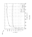
- FIG. 1 shows a tradeoff curve illustrating problems to be addressed when designing a small LED source with high brightness and high efficiency.
- FIG. 2A is a cross-section view of a wirebond LED for discussing problems to be addressed when designing a small LED source with high brightness and high efficiency.
- FIG. 2B is a cross-section view of a flip-chip LED for discussing problems to be addressed when designing a small LED source with high brightness and high efficiency.
- FIG. 3 shows a tradeoff curve of a blue-pumped thin-film design for depicting performance characteristics to be considered in the design of a small LED source with high brightness and high efficiency.
- FIG. 4 shows a tradeoff curve of a violet-pumped volumetric LED for depicting performance characteristics to be considered in the design of a small LED source with high brightness and high efficiency.
- FIG. 5 is a tradeoff curve of a violet-pumped volumetric LED design for depicting how such LEDs maintain a high performance when their footprint is scaled down for designing a small LED source with high brightness and high efficiency.
- FIG. 6A depicts an LED source placed on a high-reflectivity submount as used in the design of a small LED source with high brightness and high efficiency, according to some embodiments.
- FIG. 6B depicts an LED source with a metal-like reflector as used in the design of a small LED source with high brightness and high efficiency, according to some embodiments.
- FIG. 7 depicts an LED surrounded by a transparent layer as used in designs for a small LED source with high brightness and high efficiency, according to some embodiments.
- FIG. 8 depicts an LED with an undersized color-conversion layer as used in designs for a small LED source with high brightness and high efficiency, according to some embodiments.
- FIG. 9 depicts an LED with an oversized sized color-conversion layer as used in designs for a small LED source with high brightness and high efficiency, according to some embodiments.
- FIG. 10 A 1 and FIG. 10 A 2 depict an LED surrounded by color-conversion materials as used in designs for a small LED source with high brightness and high efficiency, according to some embodiments.
- FIG. 10B through FIG. 10F depict experimental results of devices in accordance with some of the embodiments disclosed herein.
- FIG. 11 depicts an LED with light-blocking regions flanking the LED as used in designs for a small LED source with high brightness and high efficiency, according to some embodiments.
- FIG. 12A depicts an LED with color-converting material disposed in a cavity of a volumetric LED as used in designs for a small LED source with high brightness and high efficiency, according to some embodiments.
- FIG. 12B depicts an LED with wavelength-selective reflector as used in designs for a small LED source with high brightness and high efficiency, according to some embodiments.
- FIGS. 13A-13D depict LED cross-sections during a series of fabrication steps where an LED is placed on the submount and a dam material is placed around the small LED source with high brightness and high efficiency, according to fabrication of some embodiments.
- FIGS. 14A-14D depict LED cross-sections during a series of fabrication steps where an LED is placed on the submount and a thin reflector is formed on the sides of the small LED source with high brightness and high efficiency, according to fabrication of some embodiments.
- FIGS. 15A-15C depict LED cross-sections during a series of fabrication steps where a color-conversion layer is placed on the top of the small LED source with high brightness and high efficiency, according to fabrication of some embodiments.
- FIGS. 16A-16C depict LED cross-sections during a series of fabrication steps where a color-conversion material is disposed to surround the small LED source with high brightness and high efficiency, according to fabrication of some embodiments.
- FIG. 17 depicts an electrode scheme used with an LED having a vertical chip geometry to form a small LED source with high brightness and high efficiency, according to some embodiments.
- FIG. 18 depicts an LED having a narrow n-grid that covers part of the top surface of a small LED source with high brightness and high efficiency, according to some embodiments.
- FIG. 19 depicts a flip-chip LED having a narrow n-grid that covers part of the top surface of a small LED source with high brightness and high efficiency, according to some embodiments.
- FIGS. 20 A 1 - 20 I depict examples of uses for the disclosed small LED source with high brightness and high efficiency, according to some embodiments.
- an LED source have a surface brightness of at least 800 mW/mm 2 . Assuming an operating white-light wall-plug efficiency of about 20%, such an LED should be driven at a power of about 160 mW and a current density of about 130 A/cm 2 to emit a sufficient amount of light. What is needed is an LED source that has a small surface area, and emits a sufficient optical power from substantially one surface with a sufficient efficiency.
- exemplary is used herein to mean serving as an example, instance, or illustration. Any aspect or design described herein as “exemplary” is not necessarily to be construed as preferred or advantageous over other aspects or designs. Rather, use of the word exemplary is intended to present concepts in a concrete fashion.
- logic means any combination of software or hardware that is used to implement all or part of the disclosure.
- non-transitory computer readable medium refers to any medium that participates in providing instructions to a logic processor.
- a “module” includes any mix of any portions of computer memory and any extent of circuitry including circuitry embodied as a processor.
- an object having dimensions of 100 ⁇ 100 ⁇ m 2 includes an object having an area of 10,000 ⁇ m 2 .
- an object having dimensions less than 100 ⁇ 100 ⁇ m 2 includes objects in which one of the dimensions is less than 100 ⁇ m and objects in which both dimensions are less than 100 ⁇ m such as, for example, 50 ⁇ 100 ⁇ m 2 and 50 ⁇ 50 ⁇ m 2 .
- an object having dimensions less than 100 ⁇ 100 ⁇ m 2 includes objects having an area less than 10,000 ⁇ m 2 such as, for example, 1,000 ⁇ m 2 and 100 ⁇ m 2 . Similar definitions apply to objects having dimensions greater than the indicated dimensions.
- the areas may be square, rectangular, trapezoidal, circular, oval, or any other suitable shape.
- compositions of phosphors or other wavelength-converting materials referred to in the present disclosure comprise any uses of or combinations of various wavelength-converting materials.
- Wavelength conversion materials can be crystalline (single or poly), ceramic or semiconductor particle phosphors, ceramic or semiconductor plate phosphors, organic or inorganic downconverters, upconverters (anti-stokes), nano-particles and other materials which provide wavelength conversion.
- a phosphor has two or more dopant ions (i.e. those ions following the colon in the above phosphors), this is to mean that the phosphor has at least one (but not necessarily all) of those dopant ions within the material. That is, as understood by those skilled in the art, this type of notation means that the phosphor can include any or all of those specified ions as dopants in the formulation.
- nanoparticles, quantum dots, semiconductor particles, and other types of materials can be used as wavelength converting materials.
- the list above is representative and should not be taken to include all the materials that may be utilized within embodiments described herein.
- legacy blue-pumped thin-film white LEDs with high brightness have been demonstrated.
- Such 1 mm ⁇ 1 mm chips at an injection current of 1 A have a brightness of about 700 mW/mm 2 and a wall plug efficiency (WPE) of about 23%.
- WPE wall plug efficiency
- the brightness of these LEDs can be increased by driving them at higher current densities, however, this reduces the wall-plug efficiency.
- the reduction in efficiency at high current density is due to several effects, including at least droop in internal quantum efficiency, additional heating, and higher electrical losses at high current.
- LED source that has a small surface area, and emits a sufficient optical power from substantially one surface with a sufficient efficiency.
- the appended figures and discussion thereto show how to make and use such LED sources.
- FIG. 1 shows a tradeoff curve 100 illustrating problems to be addressed when designing a small light emitting diode (LED) source with high brightness and high efficiency.
- LED light emitting diode
- FIG. 1 illustrates this tradeoff between efficiency and brightness.
- a state-of-the-art blue-pumped 1 mm 2 white LED is considered. This is a thin-film LED grown on a sapphire substrate. The LED is inserted into a system with a base temperature of 80° C. (representative of realistic display systems). The projected performance at various current densities is shown. At higher current density, brightness increases and WPE decreases. It should also be noted that reliable continuous operation of such LEDs on sapphire is usually restricted to 100 A/cm 2 and below.
- the brightness and WPE performance are sufficient for display applications, however, the source size is too large.
- the performance is negatively impacted by several effects, including:
- a fixed part of the total LED footprint is used by the n-contacts.
- FIG. 2A shows a cross-section view of a wirebond LED 2 A 00 for discussing problems to be addressed when designing a small LED source with high brightness and high efficiency.
- the LED device shown in FIG. 2A includes LED 203 , p-contact 202 , submount 208 , and wirebond ball 204 .
- FIGS. 2A and 2B Issues related to the n-contact footprint are illustrated in FIGS. 2A and 2B .
- the n-electrode occupies a minimum size of about 100 ⁇ m 2 and above.
- the presence of an n-bond pad e.g., see wirebond ball 204 ) that is used for wirebonding blocks light emitted from the active region of the LED. If one elects to emit light below the n-pad, a large fraction of the light is lost; therefore, light generation beneath the n-contact is often prevented by the introduction of a current-blocking area.
- a current-blocking area is an area where no current injection occurs (e.g., current-blocking area 203 ), and therefore no light is generated. This can, for example, be achieved by not forming a p-contact in that area—the p-contact may be replaced with an insulating dielectric layer.
- FIG. 2B shows a cross-section view of a flip-chip LED 2 B 00 for discussing problems to be addressed when designing a small LED source with high brightness and high efficiency.
- the LED device shown in FIG. 2B includes submount 208 , p-contact 202 , and n-via 206 , and shows a cross-section of LED devices in which the n-contact area occupies at least 100 ⁇ m 2 .
- FIG. 3 shows a tradeoff curve 300 of a blue-pumped thin-film design for depicting performance characteristics to be considered in the design of a small LED source with high brightness and high efficiency.
- FIG. 3 quantifies the impact that the above issues have on performance.
- FIG. 3 shows several LED footprints (e.g., 1 mm ⁇ 1 mm 302 , 150 ⁇ m ⁇ 150 ⁇ m 304 , 200 ⁇ m ⁇ 200 ⁇ m 306 , etc.). When the footprint is reduced from 1 mm ⁇ 1 mm to 200 ⁇ m ⁇ 200 ⁇ m and 150 ⁇ m ⁇ 150 ⁇ m, performance is significantly reduced.
- Embodiments of the disclosure may use either of these approaches, or combine them. Below are described embodiments following these approaches.
- the low-droop approach employs LEDs with reduced efficiency loss at high current density. This is possible, according to some embodiments, through the use of violet-pump LEDs on a bulk III-nitride substrate. These LEDs may be grown on a polar, non-polar, or semi-polar plane, and may have any shape (e.g., having a base that is square, rectangular, polygonal or rectilinear, or circular or oblong, etc.).
- FIG. 4 shows a tradeoff curve 400 of a violet-pumped volumetric LED for depicting performance characteristics to be considered in the design of a small LED source with high brightness and high efficiency.
- the numbers on the graph indicated the corresponding current density (A/cm 2 ).
- FIG. 4 shows the performance of a violet-pumped volumetric white LED 404 grown on a bulk GaN substrate, with a footprint of 250 ⁇ m ⁇ 250 ⁇ m.
- the 1 mm 2 blue-pumped thin film white LED 402 device of FIG. 1 is also shown for comparison.
- the two devices At a current density of 50 A/cm 2 , the two devices have similar performance.
- the violet-pumped white LED maintains higher performance over a wide range of current density operation. This is due to its lower efficiency droop, and also to its lower electrical resistance, which is attributable at least in-part to the use of a bulk GaN substrate.
- FIG. 5 shows a tradeoff curve 500 of a violet-pumped white volumetric LED design for depicting how such LEDs maintain a high performance when the footprint is scaled down for producing a small LED source with high brightness and high efficiency.
- FIG. 5 shows how such LEDs maintain a high performance when their footprint is scaled down. As shown, performance is only marginally affected over the range, due at least in part to the low droop and low electrical resistance of the devices. In addition, operation at high current density (200 A/cm 2 and greater) is reliable. Due to the presence of the bulk substrate, such LEDs are usually thick (100 ⁇ m to 200 ⁇ m) and emit light from all sides. In some cases, however, the LED may be thinner, for example, 50 ⁇ m thick or 10 ⁇ m thick, or thinner. In certain applications, (e.g., for display applications), it is preferred to use LEDs in a configuration such that white light is emitted only from or substantially from one surface.
- the performance of many LED configurations are shown in FIG. 5 , in particular corresponding to a footprint are of 250 ⁇ m ⁇ 250 ⁇ m 502 , 200 ⁇ m ⁇ 200 ⁇ m 504 , 150 ⁇ m ⁇ 150 ⁇ m 506 .
- Embodiments of the invention are not limited to these footprints.
- the footprint is 10 ⁇ m ⁇ 10 ⁇ m or 1 ⁇ m ⁇ 1 ⁇ m.
- FIG. 6A depicts an LED source 6 A 00 placed on a high-reflectivity submount as used in the design of a small LED source with high brightness and high efficiency.
- the LED source is placed on a high-reflectivity submount 208 .
- the top surface dimensions are 150 ⁇ m ⁇ 150 ⁇ m.
- the sidewalls of the LED are covered by a reflective material 604 .
- the top surface of the LED 606 is covered by a color-conversion material 602 such as a phosphor, with surface dimensions similar to that of the LED.
- Light is substantially emitted by the top surface of the color-conversion material.
- the sidewall reflective material 604 may be a diffuse reflector, such as a TiO 2 -based reflector, a metallic mirror, a dichroic mirror, or a combination of these elements.
- the reflective material and/or the submount comprises a diffuse reflector, a metal material, a dielectric stack, or a combination of any of the foregoing.
- the use of a high-reflectivity submount can be advantageous to reduce optical loss and thus improve optical performance.
- the reflectivity is high at the emission wavelength of the pump LED.
- the reflectivity is high in a large range of angles and wavelengths (e.g. across the visible range) to reduce optical loss for converted light.
- reflectivity is higher than 80% (or higher than 90%, or higher than 95%) across the visible range and at all incident angles of light.
- FIG. 6B depicts an LED source 6 B 00 with a metal-like reflector as used in the design of a small LED source with high brightness and high efficiency.
- the LED source is covered on its sides with a first reflective material (e.g., reflective material 604 ) that is planar to the top of the LED.
- a second reflector 607 such as a metal reflector, with a small aperture filled with the color-conversion material 602 is then placed on top of the LED.
- the second reflector serves as a light blocking material and cavity for the color-conversion material.
- FIG. 7 depicts an LED 700 surrounded by a transparent layer as used in designs for a small LED source with high brightness and high efficiency.
- the LED is surrounded by a transparent material 609 (e.g., as air or silicone).
- the transparent material 609 is located all around the LED.
- the transparent material is located only on the sides of the LED.
- the transparent material is located only on top of the LED.
- the embodiment further comprises a reflective material 604 in proximity to the LED and/or in proximity to the color conversion material. In some embodiments, an aperture is formed in the reflective material where the color conversion material is located.
- FIG. 8 depicts an LED 800 with an undersized color-conversion layer as used in designs for a small LED source with high brightness and high efficiency.
- the LED device shown in FIG. 8 includes LED 606 , submount 208 , reflective material 604 , and undersized color-conversion material 602 .
- the use of such an undersized color-conversion layer may be advantageous to further reduce the optical size of the white light-emitting surface with respect to the surface of the pump LED, thus increasing the brightness of the system.
- FIG. 9 depicts an LED 900 with an oversized sized color-conversion layer as used in designs for a small LED source with high brightness and high efficiency.
- the LED device shown in FIG. 9 includes LED 606 , submount 208 , reflective material 604 , and oversized color-conversion material 602 .
- FIG. 10 A 1 depicts an LED 10 A 100 surrounded by color-conversion material as used in designs for a small LED source with high brightness and high efficiency.
- the LED device shown in FIG. 10 A 1 includes LED 606 , submount 208 , reflective material 604 and color-conversion material 602 .
- the color-conversion material is placed in proximity to the LED and reflective material is placed in proximity to the sides of the color-conversion material.
- This configuration may be advantageous to improve the optical efficiency of the system, by limiting the deleterious backscattering of light in the LED die. Further, in this configuration the light backscattered to the siders of the LED is more substantially color-converted light (and less substantially direct pump light from the LED). Such longer-wavelength converted light incurs lower optical loss when backscattered in the die, thus improving optical efficiency.
- FIG. 10 A 2 depicts an LED 10 A 200 surrounded by color-conversion material as used in designs for a small LED source with high brightness and high efficiency.
- the LED device shown in FIG. 10 A 2 includes LED 606 , submount 208 , reflective material 604 , color-conversion material 602 , and air gap 10 A 210 .
- FIG. 10 A 2 is similar in some aspects to that of FIG. 10 A 1 , however, an air gap 10 A 210 is present in-between the color conversion material and the reflective material.
- the purpose of the air gap is to reduce the amount of light escaping the color conversion material and reaching the reflective material due to total internal reflection (TIR) at the air gap interface. This can further improve device performance as light undergoing TIR is reflected without any loss.
- the air gap has a width of 1 ⁇ m, 10 ⁇ m, 100 ⁇ m.
- the gap is formed by a low-index substance other than air.
- the color-conversion material may be formed of phosphor particles in an encapsulant with index n approximately equal to 1.4 or 1.5, and the low-index substance has an index approximately equal to 1.2 or 1.3.
- the low index may be obtained by a variety of means, for example by dielectric materials or by pores such as air pores.
- FIG. 10B shows the measured optical reflectivity spectrum of two different diffuse reflectors at normal incidence from air.
- the lower reflectivity material (reflector 2) has a reflectivity of less than 94% for wavelengths >500 nm.
- the higher reflectivity material (reflector 1) has a reflectivity of >97% for wavelengths >500 nm.
- the reflectance is only slightly wavelength dependent.
- the reflectance can have a constant value within 1% or within 5% in the range from 400 nm to 700 nm.
- the reflectance has a constant value within 1% or within 5% in the range from 450 nm to 700 nm.
- the reflectivity is higher than a given value (for example 90% or 95% or 99%) at all angles of incidence from the incoming medium (which may be air or an encapsulant).
- the reflectivity of a high reflectivity material can be 96%, 97%, 98%, 99% or 100% depending on the material composition and method of construction. These can pertain to the values coming from air, or from an encapsulating medium (such as a silicone).
- white diffuse reflector materials can be made from titanium oxide particles (rutile, anatase or brookite phase) dispersed in a matrix of silicone or epoxy. The titanium oxide particle sizes may range from 50 nm or smaller, 100 nm, 200 nm, 300 nm, 400 nm, 500 nm to 600 nm.
- the diffused white reflector can be composed of a network of polyethylene or polytetrafluoroethylene particles or fibers with inter-penetrating air pores or gaps.
- the diffuse white reflector comprises a material with air pores such as hollow silica spheres embedded in an encapsulant.
- dichroic specular reflectors can be constructed from alternating layers of dielectric material, which layers have different refractive indices.
- metallic specular reflectors can be made from smooth film of silver metal that is more than 200 nm in thickness.
- FIG. 10C shows the measured white wall plug efficiency (WPE) of LED modules (CCT of 3000K, CRI of 80, current of 80 mA and junction temperature of 85° C.) with circular light emitting areas of varying radii.
- the configuration of the LED modules is shown in FIG. 10A .
- the radius of the light-emitting region can be 3 mm, 2 mm, 1 mm, 0.5 mm, 0.25 mm, 0.1 mm or smaller. As the radii of the emitting region is reduced from 2 mm to 0.35 mm, the wall plug efficiency decreases monotonically due an increase of optical losses in the white reflector cup surrounding the light-emitting region.
- the curves compare devices built with a higher reflectivity cup (Reflector 1) and devices built with a lower reflectivity cup (Reflector 2) as shown in FIG. 10B .
- Reflector 1 For large radii (>1 mm), the effect of the reflectivity of the cup is less pronounced, the WPE difference between Reflector 1 and Reflector 2 may be less than two percent.
- small radii ⁇ 0.5 mm
- the reflectivity of the reflector material has a large effect on the WPE of the device, which could differ by more than five percent.
- FIG. 10C illustrates results of using of materials with high reflectivity (e.g., to maintain performance when the reflector becomes close to the LED emitter). Some embodiments are further reduced in footprint, and the use of high-reflectivity materials becomes more dominant in such designs.
- FIG. 10D shows the surface brightness (in W/mm 2 ) of LED modules (CCT of 3000K, CRI of 80, current of 80 mA and junction temperature of 85° C.) with circular light emitting areas of varying radii.
- CCT surface brightness
- CRI color index
- 80 current of 80 mA
- junction temperature junction temperature
- FIG. 10D shows the surface brightness (in W/mm 2 ) of LED modules (CCT of 3000K, CRI of 80, current of 80 mA and junction temperature of 85° C.) with circular light emitting areas of varying radii.
- the surface brightness increases monotonically because the total light emitted from the source is confined to a smaller area.
- the curves compare devices built with a higher reflectivity cup (Reflector 1) and devices built with a lower reflectivity cup (Reflector 2) as shown on FIG. 10B .
- the surface brightness of LEDs packaged with Reflector 1 increase more with decreasing emitting area compared to LEDs packaged with Reflector 2, which is composed of a lower reflectivity material.
- LEDs packaged with Reflector 1 exhibit 50% greater surface brightness due to lower optical losses to the reflector cup.
- the reflectivity of the cup material can be selected, managed or optimized. Given the same input current of 80 mA, the surface brightness of the source can be increased by confining the light emitting area to a smaller region, as shown in FIG. 10D . However, this comes at the cost of decreasing white WPE (as shown in FIG. 10E ) due to an increase of optical losses to the reflective cup. For LEDs assembled with a lower reflectivity material (see Reflector 2), the achievable surface brightness is severely limited because the efficiency of the source drops sharply as the light-emitting area is reduced. For LEDs assembled with a higher reflectivity material (see Reflector 1), high surface brightness can be achieved with a much lower penalty in white WPE. In the example shown in FIG. 10E , the surface brightness of LEDs assembled with Reflector 1 can be increased by more than 10 times while incurring no more than 15% loss in white WPE.
- FIG. 10F depicts WPE as a function of the height of the cup.
- the height of the cup can also dramatically impact the overall white WPE of small LED sources with less than 1 mm 2 of emitting area.
- the thickness of the reflective cup can be 0.6 mm, 0.5 mm, 0.4 mm, 0.3 mm, 0.2 mm or 0.1 mm. As shown in FIG.
- the white WPE of the source increases as the thickness of the reflective cup is reduced (the phosphor blend is tuned to maintain the same color point in each case).
- the white LED thickness determined by the cup height
- the proportion of light that impinges upon the reflective cup also decreases, resulting in less optical loss.
- FIG. 10F shows that when the height of the cup (Reflector 2) is reduced from 0.5 mm to 0.25 mm, the white WPE is increased by more than 15%. This directly translates into 15% higher surface brightness because the emitting area is maintained.
- a combined thickness of the submount, the at least one LED, and the light-converting material is less than 2 mm, less than 1 mm, and in certain embodiments, less than 0.5 mm.
- an air gap is created between the LED and the reflective material, or between the color conversion material and the reflective material. In such embodiments, the probability for light to reach the reflective material is decreased. For example, if the color conversion material surrounding the die has an index of about 1.4, only 50% of the diffuse light in the color conversion material will escape to the air gap and require reflection by the reflective material.
- the air gap may, for example, have a thickness of about 1 ⁇ m, 10 ⁇ m, 100 ⁇ m.
- FIG. 10 A 2 illustrates these embodiments.
- the reflectivity of the submount is important to maintain performance.
- Such high-reflectivity mirrors can be composed of a metallic mirror (such as silver) coated by a dielectric layer, or a series of dielectric layers acting as a dichroic.
- a low-index layer is present in the stack of the submount to obtain a total internal reflection (TIR) effect: large-angle light undergoing TIR is perfectly reflected and does not travel to lossy layers of the submount.
- TIR total internal reflection
- FIG. 11 depicts an LED 1100 with light-blocking regions flanking the LED as used in designs for a small LED source with high brightness and high efficiency.
- the LED device shown in FIG. 11 includes LED 606 , submount 208 , reflective material 604 , color-conversion material 602 , and light-blocking material 1102 .
- a light-blocking material 1102 is placed above the active region of the LED 606 to prevent emission of light that may diffuse through the reflective material 604 .
- This light-blocking material 1102 may, for example, be a metal, or a substantially-black material.
- the sidewalls of the LED need not be vertical. In some embodiments, the sidewalls of an LED can be slanted with either a positive or a negative angle from the vertical.
- the LED is thinned down so that only a small fraction of the light can escape from the sides.
- the vertical-to-horizontal aspect ratio of the LED can be less than 10%.
- no sidewall reflector is used.
- this thinning approach is combined with a sidewall reflector such as one of the reflectors described in previous embodiments.
- FIG. 12A depicts an LED 12 A 00 with color-converting material disposed in a cavity of a volumetric LED as used in designs for a small LED source with high brightness and high efficiency.
- the LED device shown in FIG. 12A includes LED 606 , submount 208 , reflective material 604 , color-conversion material 602 , and light-blocking material 1102 .
- the volumetric nature of the LED die can be used.
- a cavity is etched in the LED—for example, in the bulk GaN substrate.
- the cavity can be etched by dry etching or by chemical etching.
- This cavity is then filled with a white-emitting color-conversion material. This enables a thin LED device profile.
- the sidewalls of the LED may be coated with a reflective material, and a light-blocking material may be used to mask the bare outer edge of the LED.
- FIG. 12B depicts an LED 12 B 00 with wavelength-selective reflector 1204 as used in designs for a small LED source with high brightness and high efficiency.
- the LED device shown in FIG. 12B includes LED 606 , submount 208 , color-conversion material 602 , reflective material 604 , dam 12 B 02 , wavelength-selective reflector 1204 and metal cap 1206 .
- a wavelength-selective reflector 1204 such as a dichroic mirror is incorporated to the design. This mirror may reflect the direct emission from the LED but transmit the converted light, thus decreasing or removing the need for a color-conversion material layer on top of the LED chip.
- Some embodiments include a metal cap 1206 that creates an aperture through which the direct emissions from the LED can pass. This metal cap can be used to shrink the emitting area, for applications requiring a specific small emitting area.
- some embodiments include a dam element 12 B 02 .
- the dam can be used in some fabrication flows, for example: first the dam is placed around the LED, and then the color-conversion material is dispensed (i.e. in liquid of paste form) in the dam around the LED, and cured to reach a solid phase.
- FIGS. 13A-13D depict LED cross-sections during a series of fabrication steps (e.g., see cross-section 13 A 00 , see cross-section 13 B 00 , see cross-section 13 C 00 , see cross-section 13 D 00 ) where an LED is placed on the submount and a dam material is placed around the small LED source with high brightness and high efficiency.
- the devices shown in FIGS. 13A-13D include LED 606 , submount 208 , dam 12 B 02 , reflective material 604 , color-conversion material 602 , and light-blocking material 1102 .
- the LED is placed on the submount and a dam element 12 B 02 is placed around the LED. Part of the volume between the dam and the LED is filled with a reflective material 604 . Part of the volume around the LED is filled with color-conversion material 602 . A light-blocking layer 1102 is formed above.
- FIGS. 14A-14D depict LED cross-sections during a series of fabrication steps (e.g., see cross-section 14 A 00 , see cross-section 14 B 00 , see cross-section 14 C 00 , see cross-section 14 D 00 ) where an LED is placed on the submount and a thin reflector is formed on the sides of the small LED source with high brightness and high efficiency.
- the devices shown in FIGS. 14A-14D include LED 606 , submount 208 , reflective material 604 , and color-conversion material 602 .
- the LED is placed on the submount 208 and a thin reflector 604 (such as a metal) is formed on the sides of the LED.
- the color-conversion material 602 is the placed on top of the LED.
- a thin reflector covers both the sides of the die and color-conversion-material mesa to facilitate top-side only emissions.
- FIGS. 15A-15C depict LED cross-sections during a series of fabrication steps (e.g., see cross-section 15 A 00 , see cross-section 15 B 00 , see cross-section 15 C 00 , see cross-section 15 D 00 ) where a color-conversion layer is placed on the top of the small LED source with high brightness and high efficiency.
- the LED devices shown in FIGS. 15A-15C include LED 606 , color-conversion material 602 , tape 1502 , submount 208 , and reflective material 604 .
- the color-conversion layer is first placed on the top of the LED—for example while the LED is on a tape. The LED is then attached to the submount. Finally the reflective material is formed around the LED.
- FIGS. 16A-16C depict LED cross-sections during a series of fabrication steps 16 A 00 - 16 C 00 where a color-conversion material is disposed to surround the small LED source with high brightness and high efficiency.
- the LED devices shown in FIGS. 16A-16C include LED 606 , color-conversion material 602 , tape 1502 , submount 208 , and reflective material 604 .
- the color-conversion layer is first placed around LED (e.g., while the LED is on a tape). The LED is then attached to the submount. The reflective material is formed around the color-conversion material.
- the n-electrode occupies a minimum size of 100 ⁇ m ⁇ 100 ⁇ m and above. For a device footprint of 200 ⁇ m ⁇ 200 ⁇ m, only 75% of the device area is being used for light generation. In some embodiments of the present disclosure, the device area is 200 ⁇ m ⁇ 200 ⁇ m or less, and the light-generating area is at least 80% of the device area.
- this is obtained using a vertical chip geometry.
- FIG. 17 depicts an electrode scheme used with an LED 1700 having a vertical chip geometry to form a small LED source with high brightness and high efficiency.
- a narrow n-grid 1703 covers part of the top surface of the LED.
- the electrode runs to the side of the LED along one of the sidewalls 1704 that has been passivated, for example, by deposition of a dielectric layer (see passivated sidewall 1704 ).
- An n-wirebond ball 204 is placed away from the LED so that it does not contribute to light occlusion or shadowing or a reduction of the light generation area.
- the narrow n-grid has an area that is less than 20% of the footprint of the LED.
- a cross-section 1750 of the LED showing the p-contact 1705 (where light is generated) and a current-blocking area 1706 under the n-contact 1702 to prevent light generation there.
- FIG. 18 depicts an LED 1800 having a narrow n-grid that covers part of the top surface of a small LED source with high brightness and high efficiency.
- the n-grid runs to the side of the LED on a planarizing layer 1802 rather than on a sidewall of the LED.
- the modified electrode layout is obtained in a flip-chip technology.
- FIG. 19 depicts a flip-chip LED 1900 having a narrow n-grid that covers part of the top surface of a small LED source with high brightness and high efficiency.
- the device shown in FIG. 19 includes p-contact 202 , n-contact 1702 , and dielectric 1902 .
- the n-contact area is a small fraction of the light-emitting area.
- the submount contains several layers which reconfigure the n and p electrodes, increasing the area of the n-electrode under the LED for interconnect purposes.
- Dielectric layers e.g., dielectric 1902
- the two p-contact parts of the LED are connected laterally out of the plane of the figure.
- the n-electrode may have a cross shape or another shape in order to improve current spreading in the LED.
- any of the schemes shown or referenced in FIGS. 18 and 19 use the same area of re-contact and light-generation blocking layers near the active layer, however, flip-chip embodiments often features a guard band around the n-contact that operate to decrease the usable area for light emission.
- the flip-chip configuration is more-compatible with certain fabrication techniques, which can be used to create small emitting surfaces.
- Embodiments of the herein-disclosed LEDs can be used in various lamps and in various applications. Such lamps and applications can include automotive forward lighting or camera flash applications. The aforementioned automotive forward lighting or camera flash applications are merely some embodiments. Other lamps can include lamps that conform to fit with any one or more of a set of mechanical and electrical standards. Table 1 gives standards (see “Designation”) and corresponding characteristics.
- the base member of a lamp can be of any form factor configured to support electrical connections, which electrical connections can conform to any of a set of types or standards.
- Table 2 gives standards (see “Type”) and corresponding characteristics, including mechanical spacing between a first pin (e.g., a power pin) and a second pin (e.g., a ground pin).
- one or more light-emitting diodes 20 A 10 can be mounted on a submount or package to provide an electrical interconnection.
- the submount or package can be a ceramic, oxide, nitride, semiconductor, metal, or combination thereof, that include electrical interconnection capability 20 A 20 for the various LEDs.
- the submount or package can be mounted to a heatsink member 20 B 50 via a thermal interface.
- the LEDs can be configured to produce a desired emission spectrum, either by mixing primary emission from various LEDs, or by having the LEDs photo-excite wavelength down-conversion materials such as phosphors, semiconductors, or semiconductor nanoparticles (“quantum dots”), or a combination of any of the foregoing.
- the total light emitting surface (LES) of the LEDs and any down-conversion materials can form a light source 20 A 30 .
- One or more light sources can be interconnected into an array 20 B 20 , which is in turn in electrical contact with connectors 20 B 10 and brought into an assembly 20 B 30 .
- One or more lens elements 20 B 40 can be optically coupled to the light source.
- the lens design and properties can be selected so that the desired directional beam pattern for a lighting product is achieved for a given LES.
- the directional lighting product may be an LED module, a retrofit lamp 20 B 70 , or a lighting fixture 20 C 30 .
- an electronic driver can be provided with a surrounding member 20 B 60 , the driver to condition electrical power from an external source to render it suitable for the LED light source.
- the driver can be integrated into the retrofit lamp.
- an electronic driver is provided which conditions electrical power from an external source to make it suitable for the LED light source, with the driver either integrated into the fixture or provided externally to the fixture.
- an electronic driver can be provided to condition electrical power from an external source to render it suitable for the LED light source, with the driver either integrated into the module or provided externally to the module.
- suitable external power sources include mains AC (e.g., 120 Vrms AC or 240 Vrms AC), low-voltage AC (e.g., 12 VAC), and low-voltage DC (e.g., 12 VDC).
- the entire lighting product may be designed to fit standard form factors (e.g., ANSI form factors).
- retrofit lamp products include LED-based MR16, PAR16, PAR20, PAR30, PAR38, BR30, A19 and various other lamp types.
- fixtures include replacements for halogen-based and ceramic metal halide-based directional lighting fixtures.
- the present disclosure can be applied to non-directional lighting applications.
- one or more light-emitting diodes can be mounted on a submount or package to provide an electrical interconnection.
- the submount or package can be, for example, a ceramic, oxide, nitride, semiconductor, metal, or combination of any of the foregoing, that includes electrical interconnection capability for the various LEDs.
- the submount or package can be mounted to a heatsink member via a thermal interface.
- the LEDs can be configured to produce a desired emission spectrum, either by mixing primary emissions from various LEDs, or by having the LEDs photo-excite wavelength down-conversion materials such as phosphors, semiconductors, or semiconductor nanoparticles (“quantum dots”), or a combination thereof.
- the LEDs can be distributed to provide a desired shape of the light source. For example, one common shape is a linear light source for replacement of conventional fluorescent linear tube lamps.
- One or more optical elements can be coupled to the LEDs to provide a desired non-directional light distribution.
- the non-directional lighting product may be an LED module, a retrofit lamp, or a lighting fixture.
- an electronic driver can be provided to condition electrical power from an external source to render it suitable for the LED light source, with the driver integrated into the retrofit lamp.
- an electronic driver is provided to condition electrical power from an external source to render it suitable for the LED light source, with the driver either integrated into the fixture or provided externally to the fixture.
- an electronic driver can be provided to condition electrical power from an external source to render it suitable for the LED light source, with the driver either integrated into the module or provided externally to the module.
- Examples of external power sources include mains AC (e.g., 120 Vrms AC or 240 Vrms AC), low-voltage AC (e.g., 12 VAC), and low-voltage DC (e.g., 12 VDC).
- the entire lighting product may be designed to fit standard form factors (e.g., ANSI form factors).
- Examples of retrofit lamp products include LED-based replacements for various linear, circular, or curved fluorescent lamps. An example of a non-directional lighting product is shown in FIG. 20C .
- Such a lighting fixture can include replacements for fluorescent-based troffer luminaires.
- LEDs are mechanically secured into a package 20 C 10 , and multiple packages are arranged into a suitable shape such as linear array 20 C 20 .
- LEDs can be mounted on a submount or package to provide an electrical interconnection.
- the submount or package can be a ceramic, oxide, nitride, semiconductor, metal, or combination of any of the foregoing that include electrical interconnection capability for the various LEDs.
- the submount or package can be mounted to a heatsink member via a thermal interface.
- the LEDs can be configured to produce a desired emission spectrum, either by mixing primary emission from various LEDs, or by having the LEDs photo-excite wavelength down-conversion materials such as phosphors, semiconductors, or semiconductor nanoparticles (“quantum dots”), or a combination of any of the foregoing.
- the LEDs can be distributed to provide a desired shape of the light source.
- One common shape is a linear light source.
- the light source can be optically coupled to a lightguide for the backlight. This can be achieved by coupling at the edge of the lightguide (edge-lit), or by coupling light from behind the lightguide (direct-lit).
- the lightguide distributes light uniformly toward a controllable display, such as a liquid crystal display (LCD) panel.
- LCD liquid crystal display
- the display converts the LED light into desired images based on electrical control of light transmission and its color.
- One way to control the color is by use of filters (e.g., color filter substrate 20 D 40 , filter substrate 20 D 40 ).
- filters e.g., color filter substrate 20 D 40 , filter substrate 20 D 40 .
- multiple LEDs may be used and driven in pulsed mode to sequence the desired primary emission colors (e.g., using a red LED 20 D 30 , a green LED 20 D 10 , and a blue LED 20 D 20 ).
- Optional brightness-enhancing films may be included in the backlight “stack”. The brightness-enhancing films narrow the flat panel display emission to increase brightness at the expense of the observer viewing angle.
- An electronic driver can be provided to condition electrical power from an external source to render it suitable for the LED light source for backlighting, including any color sequencing or brightness variation per LED location (e.g., one-dimensional or two-dimensional dimming).
- external power sources include mains AC (e.g., 120 Vrms AC or 240 Vrms AC), low-voltage AC (e.g., 12 VAC), and low-voltage DC (e.g., 12 VDC).
- Examples of backlighting products are shown in FIG. 20 D 1 , FIG. 20 D 2 , FIG. 20 E 1 and FIG. 20 E 2 .
- LEDs can be mounted on a submount or on a rigid or semi-rigid package 20 F 10 to provide an electrical interconnection.
- the submount or package can be a ceramic, oxide, nitride, semiconductor, metal, or combination thereof, that include electrical interconnection capability for the various LEDs.
- the submount or package can be mounted to a heatsink member via a thermal interface.
- the LEDs can be configured to produce a desired emission spectrum, either by mixing primary emission from various LEDs, or by having the LEDs photo-excite wavelength down-conversion materials such as phosphors, semiconductors, or semiconductor nanoparticles (“quantum dots”), or a combination of any of the foregoing.
- the total light emitting surface (LES) of the LEDs and any down-conversion materials form a light source.
- One or more lens elements 20 F 20 can be optically coupled to the light source.
- the lens design and properties can be selected to produce a desired directional beam pattern for an automotive forward lighting application 20 F 30 for a given LED.
- An electronic driver can be provided to condition electrical power from an external source to render it suitable for the LED light source.
- Examples of external power sources for automotive applications include low-voltage DC (e.g., 12 VDC).
- An LED light source may perform a high-beam function, a low-beam function, a side-beam function, or any combination thereof.
- An example of an automotive forward lighting product is shown in FIG. 20F .
- the present disclosure can be applied to digital imaging applications, such as illumination for mobile-phone and digital still cameras.
- one or more light-emitting diodes can be mounted on a submount or package to provide an electrical interconnection.
- the submount or package can be, for example, a ceramic, oxide, nitride, semiconductor, metal, or combination of any of the foregoing, that include electrical interconnection capability for the various LEDs.
- the submount or package can be mounted to a circuit board member.
- the LEDs can be configured to produce a desired emission spectrum, either by mixing primary emission from various LEDs, or by having the LEDs photo-excite wavelength down-conversion materials such as phosphors, semiconductors, or semiconductor nanoparticles (“quantum dots”), or a combination thereof.
- the total light emitting surface (LES) of the LEDs and any down-conversion materials form a light source.
- One or more lens elements can be optically coupled to the light source.
- the lens design and properties can be selected so that the desired directional beam pattern for an imaging application is achieved for a given LES.
- An electronic driver can be provided to condition electrical power from an external source to render it suitable for the LED light source. Examples of suitable external power sources for imaging applications include low-voltage DC (e.g., 5 VDC).
- An LED light source may perform a high-beam function, low-beam function, side-beam function, daytime-running-light, or any combination thereof.
- An example of an imaging lighting product is shown in FIG. 20G .
- FIG. 20 is a diagram illustrating a smart phone architecture 20 H 00 .
- the smart phone 20 H 06 includes a housing, display, and interface device, which may include a button, microphone, and/or touch screen.
- a phone has a high resolution camera device, which can be used in various modes.
- An example of a smart phone can be an iPhone from Apple Inc. of Cupertino, Calif.
- a smart phone can be a Galaxy from Samsung or others.
- the smart phone may include one or more of the following features (which are found in an iPhone 4 from Apple Inc., although there can be variations), see www.apple.com:
- Embodiment of the present disclosure may be used with other electronic devices.
- suitable electronic devices include a portable electronic device, such as a media player, a cellular phone, a personal data organizer, or the like.
- a portable electronic device may include a combination of the functionalities of such devices.
- an electronic device may allow a user to connect to and communicate through the Internet or through other networks, such as local or wide area networks.
- a portable electronic device may allow a user to access the internet and to communicate using e-mail, text messaging, instant messaging, or using other forms of electronic communication.
- the electronic device may be similar to an iPod having a display screen or an iPhone available from Apple Inc.
- a device may be powered by one or more rechargeable and/or replaceable batteries. Such embodiments may be highly portable, allowing a user to carry the electronic device while traveling, working, exercising, and so forth. In this manner, and depending on the functionalities provided by the electronic device, a user may listen to music, play games or video, record video or take pictures, place and receive telephone calls, communicate with others, control other devices (e.g., via remote control and/or Bluetooth functionality), and so forth while moving freely with the device.
- the device may be sized such that it fits relatively easily into a pocket or the hand of the user. While certain embodiments of the present disclosure are described with respect to portable electronic devices, it should be noted that the presently disclosed techniques may be applicable to a wide array of other, less portable, electronic devices and systems that are configured to render graphical data, such as a desktop computer.
- FIG. 20I depicts an interconnection of components in an electronic device 20 I 00 .
- electronic devices include an enclosure or housing, a display, user input structures, and input/output connectors in addition to the aforementioned interconnection of components.
- the enclosure may be formed from plastic, metal, composite materials, or other suitable materials, or any combination thereof.
- the enclosure may protect the interior components of the electronic device from physical damage, and may also shield the interior components from electromagnetic interference (EMI).
- EMI electromagnetic interference
- the display may be a liquid crystal display (LCD), a light emitting diode (LED) based display, an organic light emitting diode (OLED) based display, or some other suitable display.
- the display may display a user interface and various other images such as logos, avatars, photos, album art, and the like.
- a display may include a touch screen through which a user may interact with the user interface.
- the display may also include various functions and/or system indicators to provide feedback to a user such as power status, call status, memory status, or the like. These indicators may be incorporated into the user interface displayed on the display.
- one or more of the user input structures can be configured to control the device, such as by controlling a mode of operation, an output level, an output type, etc.
- the user input structures may include a button to turn the device on or off.
- the user input structures may allow a user to interact with the user interface on the display.
- Embodiments of the portable electronic device may include any number of user input structures, including buttons, switches, a control pad, a scroll wheel, or any other suitable input structures.
- the user input structures may work with the user interface displayed on the device to control functions of the device and/or any interfaces or devices connected to or used by the device.
- the user input structures may allow a user to navigate a displayed user interface or to return such a displayed user interface to a default or home screen.
- a port may be a headphone jack that provides for the connection of headphones. Additionally, a port may have both input and output capabilities to provide for connection of a headset (e.g., a headphone and microphone combination).
- Embodiments of the present disclosure may include any number of input and/or output ports, such as headphone and headset jacks, universal serial bus (USB) ports, IEEE-1394 ports, and AC and/or DC power connectors.
- a device may use the input and output ports to connect to and send or receive data with any other device, such as other portable electronic devices, personal computers, printers, or the like. For example, in one embodiment, the device may connect to a personal computer via an IEEE-1394 connection to send and receive data files such as media files. Further details of the device can be found in U.S. Pat. No. 8,294,730.
- FIG. 20H is a system diagram with a smart phone according to an embodiment of the present disclosure.
- a server 20 H 02 is in electronic communication with a handheld electronic device 20 H 06 having functional components such as a processor 20 H 08 , memory 20 H 10 , graphics accelerator 20 H 12 , accelerometer 20 H 14 , communications interface 20 H 11 , compass 20 H 18 , GPS 20 H 20 , display 20 H 22 , and an input device 20 H 24 .
- Each device is not limited to the illustrated components.
- the components may be hardware, software or a combination of both.
- instructions can be input to the handheld electronic device 20 H 06 through an input device 20 H 24 that instructs the processor 20 H 08 to execute functions in an electronic imaging application.
- One potential instruction can be to generate a wireframe of a captured image of a portion of a human user.
- the processor 20 H 08 instructs the communications interface 20 H 11 to communicate with the server 20 H 02 and transfer a human wireframe or image data. The data is transferred by the communications interface 20 H 11 and either processed by the processor 20 H 08 immediately after image capture or stored in memory 20 H 10 for later use, or both.
- the processor 20 H 08 also receives information regarding the display's 20 H 22 attributes, and can calculate the orientation of the device, e.g., using information from an accelerometer 20 H 14 and/or other external data such as compass headings from a compass 20 H 18 , or GPS location from a GPS chip 20 H 20 , and the processor then uses the information to determine an orientation in which to display the image depending upon the example.
- the captured image can be drawn by the processor 20 H 08 , by a graphics accelerator 20 H 12 , or by a combination of the two.
- the processor can be the graphics accelerator 20 H 12 .
- the image can first be drawn in memory 20 H 10 or, if available, the memory directly associated with the graphics accelerator 20 H 12 .
- the methods described herein can be implemented by the processor 20 H 08 , the graphics accelerator 20 H 12 , or a combination of the two to create the image and related wireframe. Once the image or wireframe is drawn in memory, it can be displayed on the display 20 H 22 .
- FIG. 20I is a diagram of a smart phone system diagram according to an embodiment of the present disclosure.
- Computer system 20 I 00 is an example of computer hardware, software, and firmware that can be used to implement the disclosures above.
- System 20 I 00 includes a processor 20 I 26 , which is representative of any number of physically and/or logically distinct resources capable of executing software, firmware, and hardware configured to perform identified computations.
- Processor 20 I 26 communicates with a chipset 20 I 28 that can control input to and output from processor 20 I 26 .
- chipset 20 I 28 outputs information to display 20 I 42 and can read and write information to non-volatile storage 20 I 44 , which can include magnetic media and solid state media, for example.
- Chipset 20 I 28 also can read data from and write data to RAM 20 I 46 .
- a bridge 20 I 32 for interfacing with a variety of user interface components can be provided for interfacing with chipset 20 I 28 .
- Such user interface components can include a keyboard 20 I 34 , a microphone 20 I 36 , touch-detection-and-processing circuitry 20 I 38 , a pointing device such as a mouse 20 I 40 , and so on.
- inputs to system 20 I 00 can come from any of a variety of machine-generated and/or human-generated sources.
- Chipset 20 I 28 also can interface with one or more data network interfaces 20 I 30 that can have different physical interfaces.
- data network interfaces 20 I 30 can include interfaces for wired and wireless local area networks, for broadband wireless networks, as well as personal area networks.
- Some applications of the methods for generating and displaying and using the GUI disclosed herein can include receiving data over a physical interface 20 I 31 or be generated by the machine itself by a processor 20 I 26 analyzing data stored in memory 20 I 10 or 20 I 46 . Further, the machine can receive inputs from a user via a devices keyboard 20 I 34 , microphone 20 I 36 , touch device 20 I 38 , and pointing device 20 I 40 and execute appropriate functions, such as browsing functions by interpreting these inputs using processor 20 I 26 .
- the invention is used in a display system
- specific color properties of the emitted light may be desirable.
- One known way to measure color gamut in display applications is by a comparison to the NTSC gamut.
- the gamut is 50%, 70%, 90% or 100% of the NTSC gamut.
- the gamut is less than 50%, less than 70%, less than 90% , and in some embodiments, less than 100% of the NTSC gamut.
Abstract
Description
-
- 1. Using a low-droop device architecture which can be driven to a very high current density while maintaining sufficient efficiency; and
- 2. Designing the electrode scheme such that a large enough fraction of the footprint is used for light generation.
- (Ba,Sr,Ca,Mg)5(PO4)3(Cl,F,Br,OH):Eu2+, Mn2+
- (Ca,Sr,Ba)3MgSi2O8:Eu2+, Mn2+
- (Ba,Sr,Ca)MgAl10O17:Eu2+, Mn2+
- (Na,K,Rb,Cs)2[(Si,Ge,Ti,Zr,Hf,Sn)F6]:Mn4+
- (Mg,Ca,Zr,Ba,Zn)[(Si,Ge,Ti,,Zr,Hf,Sn)F6]:Mn4+
- (Mg,Ca,Sr,Ba,Zn)2SiO4:Eu2+
- (Sr,Ca,Ba)(Al,Ga)2S4:Eu2+
- (Ca,Sr)S:Eu2+,Ce3+
- (Y,Gd,Tb,La,Sm,Pr,Lu)3(Sc,Al,Ga)5O12:Ce3+
The group: - Ca1−xAlx−xySi1−x+xyN2−x−xyCxy:A
- Ca1−x−zNazM(III)x−xy−zSi1−x+xy+zN2−x−xyCxy:A
- M(II)1−x−zM(I)zM(III)x−xy−zSi1−x+xy+zN2−x−xyCxy:A
- M(II)1−x−zM(I)zM(III)x−xy−zSi1−x+xy+zN2−x−xy−2w/3CxyOw−v/2Hv:A
- M(II)1−x−zM(I)zM(III)x−xy−zSi1−x+xy+zN2−x−xy−2w/3−v/3CxyOwHv:A
wherein 0<x<1, 0<y<1, 0≦z<1, 0≦v<1, 0<w<1, x+z<1, x>xy+z, and 0<x—xy−z<1, M(II) is at least one divalent cation, M(I) is at least one monovalent cation, M(III) is at least one trivalent cation, H is at least one monovalent anion, and A is a luminescence activator doped in the crystal structure. - LaAl(Si6−zAlz)(N10−zOz):Ce3+ (wherein z=1)
- (Mg,Ca,Sr,Ma)(Y,Sc,Gd,Tb,La,Lu)2S4:Ce3+
- (Ba,Sr,Ca)xxSiyNz:Eu2+ (where 2x+4y=3z)
- (Y,Sc,Lu,Gd)2−nCanSi4N6+nC1−n:Ce3+, (wherein 0≦n≦0.5)
- (Lu,Ca,Li,Mg,Y) α-SiAlON doped with Eu2+ and/or Ce3+
- (Ca,Sr,Ba)SiO2N2:Eu2+,Ce3+
- Sr,Ca)AlSiN3:Eu2+
- CaAlSi(ON)3:Eu2+
- (Y,La,Lu)Si3N5:Ce3+
- (La,Y,Lu)3Si6N11:Ce3+
-
- 1. Using a low-droop device architecture that can be driven to a very high current density while maintaining sufficient efficiency.
- 2. Designing the electrode scheme such that a large enough fraction of the footprint is used for light generation (e.g., light is not prevented from escaping by the presence and juxtaposition of the electrode).
| TABLE 1 | |||
| Base | IEC | ||
| Diameter | 60061-1 | ||
| Desig- | (Crest of | standard | |
| nation | thread) | | sheet |
| E5 | |||
| 5 mm | Lilliput Edison Screw | 7004-25 | |
| (LES) | |||
| |
10 mm | Miniature Edison Screw | 7004-22 |
| (MES) | |||
| E11 | 11 mm | Mini-Candelabra Edison | (7004-6-1) |
| Screw (mini-can) | |||
| E12 | 12 mm | Candelabra Edison Screw | 7004-28 |
| (CES) | |||
| E14 | 14 mm | Small Edison Screw (SES) | 7004-23 |
| E17 | 17 mm | Intermediate Edison Screw | 7004-26 |
| (IES) | |||
| E26 | 26 mm | [Medium](one-inch) | 7004-21A-2 |
| Edison Screw (ES or MES) | |||
| E27 | 27 mm | [Medium]Edison Screw | 7004-21 |
| (ES) | |||
| E29 | 29 mm | [Admedium] Edison Screw | |
| (ES) | |||
| E39 | 39 mm | Single-contact (Mogul) | 7004-24-A1 |
| Giant Edison Screw (GES) | |||
| E40 | 40 mm | (Mogul) Giant Edison | 7004-24 |
| Screw (GES) | |||
| TABLE 2 | ||||
| Pin | Pin | |||
| center | dia- | |||
| Type | Standard | to center | meter | Usage |
| G4 | IEC 60061-1 | 4.0 | mm | 0.65- | MR11 and other |
| (7004-72) | 0.75 mm | small halogens of | |||
| 5/10/20 watt and | |||||
| 6/12 volt | |||||
| GU4 | IEC 60061-1 | 4.0 | mm | 0.95- | |
| (7004-108) | 1.05 mm | ||||
| GY4 | IEC 60061-1 | 4.0 | mm | 0.65- | |
| (7004-72A) | 0.75 mm | ||||
| GZ4 | IEC 60061-1 | 4.0 | mm | 0.95- | |
| (7004-64) | 1.05 mm | ||||
| G5 | IEC 60061-1 | 5 | mm | T4 and T5 | |
| (7004-52-5) | fluorescent tubes | ||||
| G5.3 | IEC 60061-1 | 5.33 | mm | 1.47- | |
| (7004-73) | 1.65 mm | ||||
| G5.3-4.8 | IEC 60061-1 | ||||
| (7004-126-1) | |||||
| GU5.3 | IEC 60061-1 | 5.33 | mm | 1.45- | |
| (7004-109) | 1.6 mm | ||||
| GX5.3 | IEC 60061-1 | 5.33 | mm | 1.45- | MR16 and other |
| (7004-73A) | 1.6 mm | small halogens of | |||
| 20/35/50 watt and | |||||
| 12/24 volt | |||||
| GY5.3 | IEC 60061-1 | 5.33 | mm | ||
| (7004-73B) | |||||
| G6.35 | IEC 60061-1 | 6.35 | mm | 0.95- | |
| (7004-59) | 1.05 mm | ||||
| GX6.35 | IEC 60061-1 | 6.35 | mm | 0.95- | |
| (7004-59) | 1.05 mm | ||||
| GY6.35 | IEC 60061-1 | 6.35 | mm | 1.2- | Halogen 100W |
| (7004-59) | 1.3 mm | 120V | |||
| GZ6.35 | IEC 60061-1 | 6.35 | mm | 0.95- | |
| (7004-59A) | 1.05 mm | ||||
| G8 | 8.0 | mm | Halogen 100W | ||
| 120V | |||||
| GY8.6 | 8.6 | mm | Halogen 100W | ||
| 120V | |||||
| G9 | IEC 60061-1 | 9.0 | mm | Halogen 120V | |
| (7004-129) | (US)/230V (EU) | ||||
| G9.5 | 9.5 | mm | 3.10- | Common for theatre | |
| 3.25 mm | use, several variants | ||||
| GU10 | 10 | mm | Twist-lock 120/230- | ||
| volt MR16 halogen | |||||
| lighting of 35/50 | |||||
| watt, since mid- | |||||
| 2000s | |||||
| G12 | 12.0 | mm | 2.35 mm | Used in theatre and | |
| single-end metal | |||||
| halide lamps | |||||
| G13 | 12.7 | mm | T8 and T12 | ||
| fluorescent tubes | |||||
| G23 | 23 | mm | 2 mm | ||
| GU24 | 24 | mm | Twist-lock for self- | ||
| ballasted compact | |||||
| fluorescents, since | |||||
| 2000s | |||||
| G38 | 38 | mm | Mostly used for | ||
| high-wattage theatre | |||||
| lamps | |||||
| GX53 | 53 | mm | Twist-lock for puck- |
| shaped under- | ||||
| cabinet compact | ||||
| fluorescents, since | ||||
| 2000s | ||||
-
- GSM model: UMTS/HSDPA/HSUPA (850, 900, 1900, 2100 MHz); GSM/EDGE (850, 900, 1800, 1900 MHz)
- CDMA model: CDMA EV-DO Rev. A (800, 1900 MHz)
- 802.11b/g/n Wi-Fi (802.11n 2.4 GHz only)
- Bluetooth 2.1+EDR wireless technology
- Assisted GPS
- Digital compass
- Wi-Fi
- Cellular
- Retina display
- 3.5-inch (diagonal) widescreen multi-touch display
- 800:1 contrast ratio (typical)
- 500 cd/m2 max brightness (typical)
- Fingerprint-resistant oleophobic coating on front and back
- Support for display of multiple languages and characters simultaneously
- 5-megapixel iSight camera
- Video recording, HD (720p) up to 30 frames per second with audio
- VGA-quality photos and video at up to 30 frames per second with the front camera
- Tap to focus video or still images
- LED flash
- Photo and video geotagging
- Built-in rechargeable lithium-ion battery
- Charging via USB to computer system or power adapter
- Talk time: Up to 7 hours on 3G, up to 14 hours on 2G (GSM)
- Standby time: Up to 300 hours
- Internet use: Up to 6 hours on 3G, up to 10 hours on Wi-Fi
- Video playback: Up to 10 hours
- Audio playback: Up to 40 hours
- Frequency response: 20 Hz to 20,000 Hz
- Audio formats supported: AAC (8 to 320 Kbps), protected AAC (from iTunes Store), HE-AAC, MP3 (8 to 320 Kbps), MP3 VBR, audible (
formats - User-configurable maximum volume limit
- Video out support at up to 720p with Apple digital AV adapter or Apple VGA adapter; 576p and 480p with Apple component AV cable; 576i and 480i with Apple composite AV cable (cables sold separately)
- Video formats supported: H.264 video up to 720p, 30 frames per second, main profile Level 3.1 with AAC-LC audio up to 160 Kbps, 48 kHz, stereo audio in .m4v, .mp4, and .mov file formats; MPEG-4 video up to 2.5 Mbps, 640 by 480 pixels, 30 frames per second, simple profile with AAC-LC audio up to 160 Kbps per channel, 48 kHz, stereo audio in .m4v, .mp4, and .mov file formats; motion JPEG (M-JPEG) up to 35 Mbps, 1280 by 720 pixels, 30 frames per second, audio in ulaw, PCM stereo audio in .avi file format
- Three-axis gyro
- Accelerometer
- Proximity sensor
- Ambient light sensor
Claims (20)
Priority Applications (4)
| Application Number | Priority Date | Filing Date | Title |
|---|---|---|---|
| US14/528,818 US9419189B1 (en) | 2013-11-04 | 2014-10-30 | Small LED source with high brightness and high efficiency |
| US15/236,898 US20160351761A1 (en) | 2013-11-04 | 2016-08-15 | Small led source with high brightness and high efficiency |
| US15/661,515 US10084121B2 (en) | 2013-11-04 | 2017-07-27 | Small LED source with high brightness and high efficiency |
| US16/139,609 US10529902B2 (en) | 2013-11-04 | 2018-09-24 | Small LED source with high brightness and high efficiency |
Applications Claiming Priority (2)
| Application Number | Priority Date | Filing Date | Title |
|---|---|---|---|
| US201361899723P | 2013-11-04 | 2013-11-04 | |
| US14/528,818 US9419189B1 (en) | 2013-11-04 | 2014-10-30 | Small LED source with high brightness and high efficiency |
Related Child Applications (1)
| Application Number | Title | Priority Date | Filing Date |
|---|---|---|---|
| US15/236,898 Continuation US20160351761A1 (en) | 2013-11-04 | 2016-08-15 | Small led source with high brightness and high efficiency |
Publications (1)
| Publication Number | Publication Date |
|---|---|
| US9419189B1 true US9419189B1 (en) | 2016-08-16 |
Family
ID=56610843
Family Applications (4)
| Application Number | Title | Priority Date | Filing Date |
|---|---|---|---|
| US14/528,818 Active US9419189B1 (en) | 2013-11-04 | 2014-10-30 | Small LED source with high brightness and high efficiency |
| US15/236,898 Abandoned US20160351761A1 (en) | 2013-11-04 | 2016-08-15 | Small led source with high brightness and high efficiency |
| US15/661,515 Active US10084121B2 (en) | 2013-11-04 | 2017-07-27 | Small LED source with high brightness and high efficiency |
| US16/139,609 Active US10529902B2 (en) | 2013-11-04 | 2018-09-24 | Small LED source with high brightness and high efficiency |
Family Applications After (3)
| Application Number | Title | Priority Date | Filing Date |
|---|---|---|---|
| US15/236,898 Abandoned US20160351761A1 (en) | 2013-11-04 | 2016-08-15 | Small led source with high brightness and high efficiency |
| US15/661,515 Active US10084121B2 (en) | 2013-11-04 | 2017-07-27 | Small LED source with high brightness and high efficiency |
| US16/139,609 Active US10529902B2 (en) | 2013-11-04 | 2018-09-24 | Small LED source with high brightness and high efficiency |
Country Status (1)
| Country | Link |
|---|---|
| US (4) | US9419189B1 (en) |
Cited By (13)
| Publication number | Priority date | Publication date | Assignee | Title |
|---|---|---|---|---|
| US20150371974A1 (en) * | 2014-06-18 | 2015-12-24 | X-Celeprint Limited | Micro assembled led displays and lighting elements |
| US20160240751A1 (en) * | 2015-02-17 | 2016-08-18 | Genesis Photonics Inc. | Light emitting device and manufacturing method thereof |
| US9831399B2 (en) | 2014-06-12 | 2017-11-28 | Genesis Photonics Inc. | Light emitting component |
| US9882096B2 (en) | 2015-03-18 | 2018-01-30 | Genesis Photonics Inc. | Light emitting diode structure and method for manufacturing the same |
| US9922963B2 (en) | 2015-09-18 | 2018-03-20 | Genesis Photonics Inc. | Light-emitting device |
| US9953956B2 (en) | 2015-03-18 | 2018-04-24 | Genesis Photonics Inc. | Package substrate and package structure using the same |
| US9997676B2 (en) | 2014-05-14 | 2018-06-12 | Genesis Photonics Inc. | Light emitting device and manufacturing method thereof |
| US10388838B2 (en) | 2016-10-19 | 2019-08-20 | Genesis Photonics Inc. | Light-emitting device and manufacturing method thereof |
| US10439111B2 (en) | 2014-05-14 | 2019-10-08 | Genesis Photonics Inc. | Light emitting device and manufacturing method thereof |
| US20200093238A1 (en) * | 2016-06-16 | 2020-03-26 | Harsh Kumar | Mobile phone case having mirrored surface and lighting |
| US10784423B2 (en) | 2017-11-05 | 2020-09-22 | Genesis Photonics Inc. | Light emitting device |
| US10854780B2 (en) | 2017-11-05 | 2020-12-01 | Genesis Photonics Inc. | Light emitting apparatus and manufacturing method thereof |
| US11024613B2 (en) * | 2019-11-06 | 2021-06-01 | Creeled, Inc. | Lumiphoric material region arrangements for light emitting diode packages |
Families Citing this family (3)
| Publication number | Priority date | Publication date | Assignee | Title |
|---|---|---|---|---|
| DE102016113269A1 (en) * | 2016-07-19 | 2018-01-25 | Osram Opto Semiconductors Gmbh | LIGHTING DEVICE FOR A MOBILE TERMINAL |
| CN109445179A (en) * | 2018-10-22 | 2019-03-08 | 青岛海信电器股份有限公司 | Light-emitting diode lamp-plate, its protection packaging method, backlight module and display device |
| CN109461723A (en) * | 2018-10-22 | 2019-03-12 | 青岛海信电器股份有限公司 | Light-emitting diode lamp-plate, its protection packaging method, backlight module and display device |
Citations (361)
| Publication number | Priority date | Publication date | Assignee | Title |
|---|---|---|---|---|
| US3283143A (en) | 1963-11-12 | 1966-11-01 | Marshall L Gosnell | Fog lens |
| US3621233A (en) | 1968-11-08 | 1971-11-16 | Harry Ferdinand Jr | Removably attached vehicular headlamp glare-diffusing filter |
| US3647522A (en) | 1970-04-29 | 1972-03-07 | Motorola Inc | Method of reclaiming and coating phosphor |
| US4065688A (en) | 1977-03-28 | 1977-12-27 | Westinghouse Electric Corporation | High-pressure mercury-vapor discharge lamp having a light output with incandescent characteristics |
| US4066868A (en) | 1974-12-26 | 1978-01-03 | National Forge Company | Temperature control method and apparatus |
| US4225904A (en) | 1978-05-18 | 1980-09-30 | Bill Linder | Fog filter for headlights |
| US4350560A (en) | 1981-08-07 | 1982-09-21 | Ferrofluidics Corporation | Apparatus for and method of handling crystals from crystal-growing furnaces |
| US4581646A (en) | 1982-09-16 | 1986-04-08 | Sony Corporation | Television receiver |
| JPH0228541Y2 (en) | 1984-07-25 | 1990-07-31 | ||
| US5005109A (en) | 1990-07-30 | 1991-04-02 | Carleton Roland A | Detachable amber lens for a vehicle |
| US5142387A (en) | 1990-04-11 | 1992-08-25 | Mitsubishi Denki Kabushiki Kaisha | Projection-type display device having light source means including a first and second concave mirrors |
| US5169486A (en) | 1991-03-06 | 1992-12-08 | Bestal Corporation | Crystal growth apparatus and process |
| US5366953A (en) | 1991-03-19 | 1994-11-22 | Conductus, Inc. | Method of forming grain boundary junctions in high temperature superconductor films |
| JPH0936430A (en) | 1995-02-23 | 1997-02-07 | Nichia Chem Ind Ltd | Nitride semiconductor light emitting element |
| US5607899A (en) | 1994-02-25 | 1997-03-04 | Sumitomo Electric Industries, Ltd. | Method of forming single-crystalline thin film |
| JPH0982587A (en) | 1995-09-08 | 1997-03-28 | Hewlett Packard Co <Hp> | Preparation of nonsquare electronic chip |
| US5632812A (en) | 1993-03-10 | 1997-05-27 | Canon Kabushiki Kaisha | Diamond electronic device and process for producing the same |
| JPH09199756A (en) | 1996-01-22 | 1997-07-31 | Toshiba Corp | Reflection-type optical coupling system |
| US5685885A (en) | 1990-09-24 | 1997-11-11 | Tessera, Inc. | Wafer-scale techniques for fabrication of semiconductor chip assemblies |
| US5764674A (en) | 1996-06-28 | 1998-06-09 | Honeywell Inc. | Current confinement for a vertical cavity surface emitting laser |
| US5813753A (en) | 1997-05-27 | 1998-09-29 | Philips Electronics North America Corporation | UV/blue led-phosphor device with efficient conversion of UV/blues light to visible light |
| US5926493A (en) | 1997-05-20 | 1999-07-20 | Sdl, Inc. | Optical semiconductor device with diffraction grating structure |
| EP0961328A2 (en) | 1998-05-28 | 1999-12-01 | Sumitomo Electric Industries, Ltd. | Gallium nitride-type semiconductor device |
| JPH11340507A (en) | 1998-05-26 | 1999-12-10 | Matsushita Electron Corp | Semiconductor light-emitting element and its manufacture |
| US6069394A (en) | 1997-04-09 | 2000-05-30 | Matsushita Electronics Corporation | Semiconductor substrate, semiconductor device and method of manufacturing the same |
| US6072197A (en) | 1996-02-23 | 2000-06-06 | Fujitsu Limited | Semiconductor light emitting device with an active layer made of semiconductor having uniaxial anisotropy |
| JP2000294883A (en) | 1999-04-05 | 2000-10-20 | Nec Corp | Nitride compound semiconductor laser element |
| US6147953A (en) | 1998-03-25 | 2000-11-14 | Duncan Technologies, Inc. | Optical signal transmission apparatus |
| US6195381B1 (en) | 1998-04-27 | 2001-02-27 | Wisconsin Alumni Research Foundation | Narrow spectral width high-power distributed feedback semiconductor lasers |
| JP2001160627A (en) | 1999-11-30 | 2001-06-12 | Toyoda Gosei Co Ltd | Group iii nitride compound semiconductor light emitting element |
| JP2001177146A (en) | 1999-12-21 | 2001-06-29 | Mitsubishi Cable Ind Ltd | Triangular shape semiconductor element and manufacturing method therefor |
| US20010009134A1 (en) | 1998-10-15 | 2001-07-26 | Lg Electronics Inc. | GaN system compound semiconductor and method for growing crystal thereof |
| US6275145B1 (en) | 1996-03-07 | 2001-08-14 | Joseph Rogozinski | Apparatus to help prevent temporary blinding of drivers |
| US20010022495A1 (en) | 1998-11-19 | 2001-09-20 | Salam Hassan P. A. | LED lamps |
| US20010043042A1 (en) | 1998-08-18 | 2001-11-22 | Yoshinori Murazaki | Red light emitting long afterglow photoluminescence phosphor and afterglow lamp thereof |
| US6335771B1 (en) | 1996-11-07 | 2002-01-01 | Sharp Kabushiki Kaisha | Liquid crystal display device, and methods of manufacturing and driving same |
| US20020027933A1 (en) | 2000-07-18 | 2002-03-07 | Rohm Co., Ltd. | Semiconductor light emitting device and semiconductor laser |
| US6379985B1 (en) | 2001-08-01 | 2002-04-30 | Xerox Corporation | Methods for cleaving facets in III-V nitrides grown on c-face sapphire substrates |
| US20020050488A1 (en) | 2000-03-01 | 2002-05-02 | Dmitri Nikitin | Method and apparatus for thermally processing quartz using a plurality of laser beams |
| US20020070416A1 (en) | 1999-12-09 | 2002-06-13 | The Regents Of The University Of California | Current isolating epitaxial buffer layers for high voltage photodiode array |
| JP2002185085A (en) | 2000-12-12 | 2002-06-28 | Sharp Corp | Nitride-based semiconductor laser element and method of dividing chip |
| US20020096994A1 (en) | 2000-07-18 | 2002-07-25 | Toshiaki Iwafuchi | Image display unit and method of producing image display unit |
| US20020127824A1 (en) | 1998-10-23 | 2002-09-12 | Shelton Bryan S. | Semiconductor wafer protection and cleaning for device separation using laser ablation |
| US20020190260A1 (en) | 1999-12-22 | 2002-12-19 | Yu-Chen Shen | Selective placement of quantum wells in flipchip light emitting diodes for improved light extraction |
| US6498355B1 (en) | 2001-10-09 | 2002-12-24 | Lumileds Lighting, U.S., Llc | High flux LED array |
| US6501154B2 (en) | 1997-06-03 | 2002-12-31 | Sony Corporation | Semiconductor substrate made of a nitride III-V compound semiconductor having a wurtzite-structured crystal structure |
| US20030001238A1 (en) | 2001-06-06 | 2003-01-02 | Matsushita Electric Industrial Co., Ltd. | GaN-based compound semiconductor EPI-wafer and semiconductor element using the same |
| US20030000453A1 (en) | 2001-06-27 | 2003-01-02 | Yasuyuki Unno | Optical element and manufacturing method thereof |
| US20030020087A1 (en) | 2001-04-24 | 2003-01-30 | Osamu Goto | Nitride semiconductor, semiconductor device, and method of manufacturing the same |
| JP2003031844A (en) | 2001-07-11 | 2003-01-31 | Sony Corp | Method of manufacturing semiconductor light emitting device |
| US20030045042A1 (en) | 2001-08-03 | 2003-03-06 | Goshi Biwa | Method of fabricating semiconductor device and semiconductor device |
| US20030047076A1 (en) | 2001-09-10 | 2003-03-13 | Liu Jean H. | Dynamic filtration method and apparatus for separating nano powders |
| US6533874B1 (en) | 1996-12-03 | 2003-03-18 | Advanced Technology Materials, Inc. | GaN-based devices using thick (Ga, Al, In)N base layers |
| US20030080345A1 (en) | 2001-09-19 | 2003-05-01 | Sumitomo Electric Industries, Ltd. | Single crystal GaN substrate, method of growing same and method of producing same |
| US6586762B2 (en) | 2000-07-07 | 2003-07-01 | Nichia Corporation | Nitride semiconductor device with improved lifetime and high output power |
| US20030164507A1 (en) | 2000-11-03 | 2003-09-04 | Edmond John Adam | Group III nitride light emitting devices with progressively graded layers |
| US20030178617A1 (en) | 2002-03-20 | 2003-09-25 | International Business Machines Corporation | Self-aligned nanotube field effect transistor and method of fabricating same |
| US20030216011A1 (en) | 1992-11-20 | 2003-11-20 | Nichia Chemical Industries Ltd. | Light-emitting gallium nitride-based compound semiconductor device |
| US20040051107A1 (en) | 2001-03-28 | 2004-03-18 | Shinichi Nagahama | Nitride semiconductor element |
| US20040070004A1 (en) | 2000-11-16 | 2004-04-15 | Ivan Eliashevich | Led packages having improved light extraction |
| US20040080256A1 (en) | 1997-02-24 | 2004-04-29 | Hampden-Smith Mark J. | Oxygen-containing phosphor powders, methods for making phosphor powders and devices incorporating same |
| US6734461B1 (en) | 1999-09-07 | 2004-05-11 | Sixon Inc. | SiC wafer, SiC semiconductor device, and production method of SiC wafer |
| US20040116033A1 (en) | 2003-01-27 | 2004-06-17 | 3M Innovative Properties Company | Methods of making phosphor based light sources having an interference reflector |
| JP2004179644A (en) | 2002-11-12 | 2004-06-24 | Nichia Chem Ind Ltd | Phosphor lamination and light source using the same |
| US20040124435A1 (en) | 2002-12-27 | 2004-07-01 | General Electric Company | Homoepitaxial gallium-nitride-based electronic devices and method for producing same |
| US20040161222A1 (en) | 2003-02-18 | 2004-08-19 | Eiki Niida | Optical waveguide, area light source device and liquid crystal display device |
| US20040164308A1 (en) | 2001-10-12 | 2004-08-26 | Tsunenori Asatsuma | Method of manufacturing a semiconductor light emitting device, semiconductor light emitting device, method of manufacturing a semiconductor device, semiconductor device, method of manufacturing a device, and device |
| US20040190304A1 (en) | 2001-07-26 | 2004-09-30 | Masaru Sugimoto | Light emitting device using led |
| US20040196877A1 (en) | 2003-04-01 | 2004-10-07 | Sharp Kabushiki Kaisha | Multi-wavelength laser device |
| US6809781B2 (en) | 2002-09-24 | 2004-10-26 | General Electric Company | Phosphor blends and backlight sources for liquid crystal displays |
| US20040227149A1 (en) | 2003-04-30 | 2004-11-18 | Cree, Inc. | High powered light emitter packages with compact optics |
| US20040245543A1 (en) | 2003-06-04 | 2004-12-09 | Yoo Myung Cheol | Method of fabricating vertical structure compound semiconductor devices |
| US20050001227A1 (en) | 2001-07-24 | 2005-01-06 | Nichia Corporation | Semiconductor light-emitting device |
| US20050012446A1 (en) | 2003-05-28 | 2005-01-20 | Frank Jermann | Conversion led |
| US6853010B2 (en) | 2002-09-19 | 2005-02-08 | Cree, Inc. | Phosphor-coated light emitting diodes including tapered sidewalls, and fabrication methods therefor |
| US6860628B2 (en) | 2002-07-17 | 2005-03-01 | Jonas J. Robertson | LED replacement for fluorescent lighting |
| US20050045894A1 (en) | 2000-12-15 | 2005-03-03 | Hiroyuki Okuyama | Semiconductor light emitting device and fabrication method thereof |
| US6864641B2 (en) | 2003-02-20 | 2005-03-08 | Visteon Global Technologies, Inc. | Method and apparatus for controlling light emitting diodes |
| US20050084218A1 (en) | 2003-09-08 | 2005-04-21 | Seiko Epson Corporation | Optical module, and optical transmission device |
| US20050087753A1 (en) | 2003-10-24 | 2005-04-28 | D'evelyn Mark P. | Group III-nitride based resonant cavity light emitting devices fabricated on single crystal gallium nitride substrates |
| US6889006B2 (en) | 2003-06-02 | 2005-05-03 | Toda Seiko Co., Ltd. | Auxiliary lens for camera and the like |
| US20050121679A1 (en) | 1997-01-09 | 2005-06-09 | Nichia Chemical Industries, Ltd. | Nitride semiconductor device |
| US20050140270A1 (en) | 2003-12-02 | 2005-06-30 | Henson Gordon D. | Solid state light device |
| US20050167680A1 (en) | 2004-02-02 | 2005-08-04 | Shih-Chang Shei | Light-emitting diode structure with electrostatic discharge protection |
| US20050199899A1 (en) | 2004-03-11 | 2005-09-15 | Ming-Der Lin | Package array and package unit of flip chip LED |
| US20050214992A1 (en) | 2002-12-16 | 2005-09-29 | The Regents Of The University Of California | Fabrication of nonpolar indium gallium nitride thin films, heterostructures and devices by metalorganic chemical vapor deposition |
| US20050224830A1 (en) | 2004-04-09 | 2005-10-13 | Blonder Greg E | Illumination devices comprising white light emitting diodes and diode arrays and method and apparatus for making them |
| US6956246B1 (en) | 2004-06-03 | 2005-10-18 | Lumileds Lighting U.S., Llc | Resonant cavity III-nitride light emitting devices fabricated by growth substrate removal |
| US20050230701A1 (en) | 2004-04-16 | 2005-10-20 | Wen-Chieh Huang | High brightness gallium nitride-based light emitting diode with transparent conducting oxide spreading layer |
| US20050232327A1 (en) | 2004-03-30 | 2005-10-20 | Yasuhiko Nomura | Integrated semiconductor laser diode module and manufacturing method of the same |
| US20050263791A1 (en) | 2003-01-17 | 2005-12-01 | Sanken Electric Co., Ltd. | Semiconductor device and a method of making the same |
| US20060006404A1 (en) | 2004-06-30 | 2006-01-12 | James Ibbetson | Chip-scale methods for packaging light emitting devices and chip-scale packaged light emitting devices |
| US6989807B2 (en) | 2003-05-19 | 2006-01-24 | Add Microtech Corp. | LED driving device |
| US20060038542A1 (en) | 2003-12-23 | 2006-02-23 | Tessera, Inc. | Solid state lighting device |
| US7009199B2 (en) | 2002-10-22 | 2006-03-07 | Cree, Inc. | Electronic devices having a header and antiparallel connected light emitting diodes for producing light from AC current |
| US7012279B2 (en) | 2003-10-21 | 2006-03-14 | Lumileds Lighting U.S., Llc | Photonic crystal light emitting device |
| US20060060131A1 (en) | 2003-12-29 | 2006-03-23 | Translucent, Inc. | Method of forming a rare-earth dielectric layer |
| US7019325B2 (en) | 2004-06-16 | 2006-03-28 | Exalos Ag | Broadband light emitting device |
| US20060068154A1 (en) | 2004-01-15 | 2006-03-30 | Nanosys, Inc. | Nanocrystal doped matrixes |
| US20060065900A1 (en) | 2004-09-24 | 2006-03-30 | Min-Hsun Hsieh | Liquid crystal display |
| US20060077795A1 (en) | 2004-09-01 | 2006-04-13 | Fujinon Corporation | Objective optical system for optical recording media and optical pickup device using it |
| US20060079082A1 (en) | 2002-07-19 | 2006-04-13 | Cree, Inc. | Trench cut light emitting diodes and methods of fabricating same |
| US20060097385A1 (en) | 2004-10-25 | 2006-05-11 | Negley Gerald H | Solid metal block semiconductor light emitting device mounting substrates and packages including cavities and heat sinks, and methods of packaging same |
| JP2006147933A (en) | 2004-11-22 | 2006-06-08 | Matsushita Electric Works Ltd | Light emitting diode illuminating device |
| US20060124051A1 (en) | 2003-04-03 | 2006-06-15 | Mitsubishi Chemical Corporation | Zinc oxide single crystal |
| JP2006173621A (en) | 2004-12-14 | 2006-06-29 | Palo Alto Research Center Inc | Semiconductor laser |
| US20060152795A1 (en) | 2005-01-07 | 2006-07-13 | Miradia Inc. | Electrical contact method and structure for deflection devices formed in an array configuration |
| US7081722B1 (en) | 2005-02-04 | 2006-07-25 | Kimlong Huynh | Light emitting diode multiphase driver circuit and method |
| US20060163589A1 (en) | 2005-01-21 | 2006-07-27 | Zhaoyang Fan | Heterogeneous integrated high voltage DC/AC light emitter |
| US20060166390A1 (en) | 2005-01-13 | 2006-07-27 | Fabrice Letertre | Optoelectronic substrate and methods of making same |
| US7083302B2 (en) | 2004-03-24 | 2006-08-01 | J. S. Technology Co., Ltd. | White light LED assembly |
| US20060169993A1 (en) | 2005-02-03 | 2006-08-03 | Zhaoyang Fan | Micro-LED based high voltage AC/DC indicator lamp |
| US20060177362A1 (en) | 2005-01-25 | 2006-08-10 | D Evelyn Mark P | Apparatus for processing materials in supercritical fluids and methods thereof |
| US20060180828A1 (en) | 2005-02-17 | 2006-08-17 | Lg Electronics Inc. | Light source apparatus and fabrication method thereof |
| US20060186418A1 (en) | 2004-05-18 | 2006-08-24 | Edmond John A | External extraction light emitting diode based upon crystallographic faceted surfaces |
| US20060189098A1 (en) | 2005-02-23 | 2006-08-24 | Cree, Inc. | Substrate removal process for high light extraction LEDs |
| US20060204865A1 (en) | 2005-03-08 | 2006-09-14 | Luminus Devices, Inc. | Patterned light-emitting devices |
| US20060208262A1 (en) | 2005-03-18 | 2006-09-21 | Fujikura Ltd., Independent Administrative Institution | Light emitting device and illumination apparatus |
| US20060214287A1 (en) | 2005-03-25 | 2006-09-28 | Mitsuhiko Ogihara | Semiconductor composite apparatus, print head, and image forming apparatus |
| US7128849B2 (en) | 2003-10-31 | 2006-10-31 | General Electric Company | Phosphors containing boron and metals of Group IIIA and IIIB |
| US20060255343A1 (en) | 2005-05-12 | 2006-11-16 | Oki Data Corporation | Semiconductor apparatus, print head, and image forming apparatus |
| US20060256482A1 (en) | 2005-05-10 | 2006-11-16 | Hitachi Global Storage Technologies Netherlands, B.V. | Method to fabricate side shields for a magnetic sensor |
| US20060261364A1 (en) | 2003-03-10 | 2006-11-23 | Yoshinobu Suehiro | Solid element device and method for manufacturing thereof |
| US7148515B1 (en) | 2006-01-07 | 2006-12-12 | Tyntek Corp. | Light emitting device having integrated rectifier circuit in substrate |
| US20060288927A1 (en) | 2005-06-24 | 2006-12-28 | Robert Chodelka | System and high pressure, high temperature apparatus for producing synthetic diamonds |
| US20060288928A1 (en) | 2005-06-10 | 2006-12-28 | Chang-Beom Eom | Perovskite-based thin film structures on miscut semiconductor substrates |
| US20070045200A1 (en) | 2005-08-30 | 2007-03-01 | Moon Won J | Gathering method and apparatus of powder separated soluble component |
| US20070054476A1 (en) | 2005-09-05 | 2007-03-08 | Sumitomo Electric Industries. Ltd. | Method of producing a nitride semiconductor device and nitride semiconductor device |
| US7193246B1 (en) | 1998-03-12 | 2007-03-20 | Nichia Corporation | Nitride semiconductor device |
| JP2007507115A (en) | 2003-10-01 | 2007-03-22 | エナートロン, インコーポレイテッド | Method and apparatus for LED light engine |
| US20070062440A1 (en) | 2001-09-19 | 2007-03-22 | Sumitomo Electric Industries Ltd. | Gallium nitride crystal substrate and method of producing same |
| US20070072324A1 (en) | 2005-09-27 | 2007-03-29 | Lumileds Lighting U.S., Llc | Substrate for growing a III-V light emitting device |
| US20070091608A1 (en) | 2004-02-12 | 2007-04-26 | Hymite A/S | Light Transmitting Modules With Optical Power Monitoring |
| US20070096239A1 (en) | 2005-10-31 | 2007-05-03 | General Electric Company | Semiconductor devices and methods of manufacture |
| US20070105351A1 (en) | 1997-10-30 | 2007-05-10 | Kensaku Motoki | GaN single crystal substrate and method of making the same |
| US20070114569A1 (en) | 2005-09-07 | 2007-05-24 | Cree, Inc. | Robust transistors with fluorine treatment |
| US20070114563A1 (en) | 2005-11-18 | 2007-05-24 | Samsung Electronics Co., Ltd. | Semiconductor device and method of fabricating the same |
| US20070121690A1 (en) | 2003-12-09 | 2007-05-31 | Tetsuo Fujii | Highly efficient gallium nitride based light emitting diodes via surface roughening |
| US20070131967A1 (en) | 2005-12-08 | 2007-06-14 | Hitachi Cable, Ltd. | Self-standing GaN single crystal substrate, method of making same, and method of making a nitride semiconductor device |
| US20070170450A1 (en) | 2006-01-20 | 2007-07-26 | Thomas Murphy | Package for a light emitting element with integrated electrostatic discharge protection |
| US7252408B2 (en) | 2004-07-19 | 2007-08-07 | Lamina Ceramics, Inc. | LED array package with internal feedback and control |
| US20070181895A1 (en) | 2004-03-18 | 2007-08-09 | Hideo Nagai | Nitride based led with a p-type injection region |
| US20070202624A1 (en) | 2006-02-24 | 2007-08-30 | Samsung Electro-Mechanics Co., Ltd. | Nitride-based semiconductor light-emitting device and method of manufacturing the same |
| US20070217462A1 (en) | 2006-03-14 | 2007-09-20 | Sharp Kabushiki Kaisha | Nitride semiconductor laser device and method of producing the same |
| US7279040B1 (en) | 2005-06-16 | 2007-10-09 | Fairfield Crystal Technology, Llc | Method and apparatus for zinc oxide single crystal boule growth |
| US7285801B2 (en) | 2004-04-02 | 2007-10-23 | Lumination, Llc | LED with series-connected monolithically integrated mesas |
| US7303630B2 (en) | 2003-11-05 | 2007-12-04 | Sumitomo Electric Industries, Ltd. | Method of growing GaN crystal, method of producing single crystal GaN substrate, and single crystal GaN substrate |
| US20070290224A1 (en) | 2006-06-15 | 2007-12-20 | Sharp Kabushiki Kaisha | Method of manufacturing nitride semiconductor light-emitting element and nitride semiconductor light-emitting element |
| US7318651B2 (en) | 2003-12-18 | 2008-01-15 | Avago Technologies Ecbu Ip (Singapore) Pte. Ltd. | Flash module with quantum dot light conversion |
| US20080023691A1 (en) | 2006-06-23 | 2008-01-31 | Jang Jun H | Light emitting diode having vertical topology and method of making the same |
| US20080030976A1 (en) | 2006-08-03 | 2008-02-07 | Yoshinori Murazaki | Light emitting apparatus |
| US20080054290A1 (en) | 2006-09-05 | 2008-03-06 | Epistar Corporation | Light emitting device and the manufacture method thereof |
| US7341880B2 (en) | 2003-09-17 | 2008-03-11 | Luminus Devices, Inc. | Light emitting device processes |
| US7348600B2 (en) | 2003-10-20 | 2008-03-25 | Nichia Corporation | Nitride semiconductor device, and its fabrication process |
| US20080073660A1 (en) | 2006-09-27 | 2008-03-27 | Mitsubishi Electric Corporation | Semiconductor light-emitting devices |
| US20080083929A1 (en) | 2006-10-06 | 2008-04-10 | Iii-N Technology, Inc. | Ac/dc light emitting diodes with integrated protection mechanism |
| US7358543B2 (en) | 2005-05-27 | 2008-04-15 | Avago Technologies Ecbu Ip (Singapore) Pte. Ltd. | Light emitting device having a layer of photonic crystals and a region of diffusing material and method for fabricating the device |
| US7358542B2 (en) | 2005-02-02 | 2008-04-15 | Lumination Llc | Red emitting phosphor materials for use in LED and LCD applications |
| US20080087919A1 (en) | 2006-10-08 | 2008-04-17 | Tysoe Steven A | Method for forming nitride crystals |
| US20080101071A1 (en) * | 2006-10-31 | 2008-05-01 | Noboru Imai | Led module |
| US20080106212A1 (en) | 2006-11-08 | 2008-05-08 | Industrial Technology Research Institute | Alternating current light-emitting device and fabrication method thereof |
| US20080121913A1 (en) | 2006-11-28 | 2008-05-29 | Mesophotonics Limited | Inverted-pyramidal photonic crystal light emitting device |
| US20080121906A1 (en) | 2004-08-20 | 2008-05-29 | Kenji Yakushiji | Method for Fabrication of Semiconductor Light-Emitting Device and the Device Fabricated by the Method |
| US20080128752A1 (en) | 2006-11-13 | 2008-06-05 | Cree, Inc. | GaN based HEMTs with buried field plates |
| US20080142781A1 (en) | 2004-12-23 | 2008-06-19 | Lg Innotek Co., Ltd. | Nitride Semiconductor Light Emitting Device and Fabrication Method Thereof |
| US7390359B2 (en) | 2004-10-06 | 2008-06-24 | Sumitomo Electric Industries, Ltd. | Nitride semiconductor wafer |
| US20080151543A1 (en) | 2006-04-21 | 2008-06-26 | Xiaoping Wang | Ultra thin power led light with heat sink |
| US20080164489A1 (en) | 2006-12-11 | 2008-07-10 | The Regents Of The University Of California | Metalorganic chemical vapor deposittion (MOCVD) growth of high performance non-polar III-nitride optical devices |
| US20080164578A1 (en) | 2006-12-28 | 2008-07-10 | Saint-Gobain Ceramics & Plastics, Inc. | Sapphire substrates and methods of making same |
| US20080173884A1 (en) | 2007-01-22 | 2008-07-24 | Cree, Inc. | Wafer level phosphor coating method and devices fabricated utilizing method |
| US20080179610A1 (en) | 2006-10-23 | 2008-07-31 | Rohm Co., Ltd. | Semiconductor light emission device emitting polarized light and method for manufacturing the same |
| US20080179607A1 (en) | 2006-12-11 | 2008-07-31 | The Regents Of The University Of California | Non-polar and semi-polar light emitting devices |
| WO2008091846A2 (en) | 2007-01-22 | 2008-07-31 | Cree Led Lighting Solutions, Inc. | Illumination devices using externally interconnected arrays of light emitting devices, and methods of fabricating same |
| US20080191192A1 (en) | 2007-02-12 | 2008-08-14 | The Regents Of The University Of California | Al(x)Ga(1-x)N-CLADDING-FREE NONPOLAR III-NITRIDE BASED LASER DIODES AND LIGHT EMITTING DIODES |
| US20080194054A1 (en) | 2007-02-08 | 2008-08-14 | Hung-Yi Lin | Led array package structure having silicon substrate and method of making the same |
| US20080191223A1 (en) | 2007-02-12 | 2008-08-14 | The Regents Of The University Of California | CLEAVED FACET (Ga,Al,In)N EDGE-EMITTING LASER DIODES GROWN ON SEMIPOLAR BULK GALLIUM NITRIDE SUBSTRATES |
| US20080206925A1 (en) | 2007-02-23 | 2008-08-28 | Dilip Kumar Chatterjee | Methods and apparatus to improve frit-sealed glass package |
| US20080217745A1 (en) | 2006-12-19 | 2008-09-11 | Sumitomo Electric Industries, Ltd. | Nitride Semiconductor Wafer |
| US20080230765A1 (en) | 2007-03-19 | 2008-09-25 | Seoul Opto Device Co., Ltd. | Light emitting diode |
| US20080237569A1 (en) | 2007-03-26 | 2008-10-02 | Kabushiki Kaisha Toshiba | Semiconductor light emitting element, method for manufacturing the same, and light emitting device |
| US20080261381A1 (en) | 2007-04-18 | 2008-10-23 | Shin-Etsu Chemical Co., Ltd. | Method for manufacturing bonded substrate |
| JP2008263154A (en) | 2007-04-11 | 2008-10-30 | Everlight Electronics Co Ltd | Phosphor-powder-application process of light-emitting diode |
| US20080282978A1 (en) | 2002-05-17 | 2008-11-20 | Kenneth Scott Alexander Butcher | Process For Manufacturing A Gallium Rich Gallium Nitride Film |
| US20080283851A1 (en) | 2007-05-17 | 2008-11-20 | Sumitomo Electric Industries, Ltd. | GaN Substrate, and Epitaxial Substrate and Semiconductor Light-Emitting Device Employing the Substrate |
| US20080284346A1 (en) | 2007-05-18 | 2008-11-20 | Samsung Electro-Mechanics Co., Ltd. | Light emitting diode array driving apparatus |
| US20080291961A1 (en) | 2005-12-16 | 2008-11-27 | Takeshi Kamikawa | Nitride semiconductor light emitting device and method of fabricating nitride semiconductor laser device |
| US20080298409A1 (en) | 2007-05-31 | 2008-12-04 | Sharp Kabushiki Kaisha | Nitride semiconductor laser chip and fabrication method thereof |
| US20080303033A1 (en) | 2007-06-05 | 2008-12-11 | Cree, Inc. | Formation of nitride-based optoelectronic and electronic device structures on lattice-matched substrates |
| JP2008311640A (en) | 2007-05-16 | 2008-12-25 | Rohm Co Ltd | Semiconductor laser diode |
| US7470555B2 (en) | 2000-06-08 | 2008-12-30 | Nichia Corporation | Semiconductor laser device, and method of manufacturing the same |
| US20090028204A1 (en) | 2007-07-24 | 2009-01-29 | Sanyo Electric Co., Ltd. | Semiconductor laser device |
| JP2009021824A (en) | 2007-07-12 | 2009-01-29 | Mitsubishi Electric Corp | Directional coupler |
| US20090032828A1 (en) | 2007-08-03 | 2009-02-05 | Philips Lumileds Lighting Company, Llc | III-Nitride Device Grown on Edge-Dislocation Template |
| US7489441B2 (en) | 2004-05-17 | 2009-02-10 | Carl Zeiss Smt Ag | Monocrystalline optical component with curved surface and multilayer coating |
| US7491984B2 (en) | 2000-03-31 | 2009-02-17 | Toyoda Gosei Co., Ltd. | Method for fabricating group III nitride compound semiconductors and group III nitride compound semiconductor devices |
| US20090058532A1 (en) | 2007-08-31 | 2009-03-05 | Fujitsu Limited | Nitride semiconductor device, doherty amplifier and drain voltage controlled amplifier |
| US20090065798A1 (en) | 2005-06-21 | 2009-03-12 | The Regents Of The University Of California | Packaging technique for the fabrication of polarized light emitting diodes |
| US20090072252A1 (en) | 2004-10-19 | 2009-03-19 | Hyo Kun Son | Nitride Semiconductor Light Emitting Device and Fabrication Method Therefor |
| US20090071394A1 (en) | 2001-10-09 | 2009-03-19 | Sumitomo Electronic Industries, Ltd. | AlxInyGa1-x-yN MIXTURE CRYSTAL SUBSTRATE, METHOD OF GROWING AlxInyGa1-x-yN MIXTURE CRYSTAL SUBSTRATE AND METHOD OF PRODUCING AlxInyGa1-x-yN MIXTURE CRYSTAL SUBSTRATE |
| US20090078955A1 (en) | 2007-09-26 | 2009-03-26 | Iii-N Technlogy, Inc | Micro-Emitter Array Based Full-Color Micro-Display |
| US20090078944A1 (en) | 2007-09-07 | 2009-03-26 | Rohm Co., Ltd. | Light emitting device and method of manufacturing the same |
| US20090081857A1 (en) | 2007-09-14 | 2009-03-26 | Kyma Technologies, Inc. | Non-polar and semi-polar GaN substrates, devices, and methods for making them |
| US20090086475A1 (en) | 2007-10-01 | 2009-04-02 | Intematix Corporation | Color tunable light emitting device |
| US20090095973A1 (en) | 2007-09-27 | 2009-04-16 | Rohm Co., Ltd. | Semiconductor light emitting device |
| WO2009066430A1 (en) | 2007-11-19 | 2009-05-28 | Panasonic Corporation | Semiconductor light emitting device and method for manufacturing semiconductor light emitting device |
| US20090146170A1 (en) | 2007-11-30 | 2009-06-11 | The Regents Of The University Of California | High light extraction efficiency nitride based light emitting diode by surface roughening |
| US20090155989A1 (en) | 2005-06-06 | 2009-06-18 | Sumitomo Electric Industries, Ltd. | Nitride semiconductor substrate and method of producing same |
| US20090173958A1 (en) | 2008-01-04 | 2009-07-09 | Cree, Inc. | Light emitting devices with high efficiency phospor structures |
| US7560981B2 (en) | 2006-11-16 | 2009-07-14 | Chunghwa Picture Tubes, Ltd. | Controlling apparatus for controlling a plurality of LED strings and related light modules |
| US7566639B2 (en) | 2005-09-16 | 2009-07-28 | Rohm Co., Ltd. | Manufacturing method for nitride semiconductor device and nitride semiconductor light emitting device obtained with the same |
| US20090206354A1 (en) | 2008-02-20 | 2009-08-20 | Hitachi Cable, Ltd. | Semiconductor light-emitting device |
| US20090226139A1 (en) | 2008-01-31 | 2009-09-10 | Coretek Opto Corp. | Optoelectronic component and optical subassembly for optical communication |
| US7598104B2 (en) | 2006-11-24 | 2009-10-06 | Agency For Science, Technology And Research | Method of forming a metal contact and passivation of a semiconductor feature |
| US20090262516A1 (en) | 2008-01-17 | 2009-10-22 | Intematix Corporation | Light emitting device with phosphor wavelength conversion |
| US20090267100A1 (en) | 2008-04-25 | 2009-10-29 | Sanyo Electric Co., Ltd. | Nitride-based semiconductor device and method of manufacturing the same |
| US20090267098A1 (en) | 2008-04-24 | 2009-10-29 | Sung Min Choi | Semiconductor light emitting device |
| US20090273005A1 (en) | 2006-07-24 | 2009-11-05 | Hung-Yi Lin | Opto-electronic package structure having silicon-substrate and method of forming the same |
| JP2009267164A (en) | 2008-04-25 | 2009-11-12 | Kyocera Corp | Light emitting device and method of manufacturing the light emitting device |
| US20090302338A1 (en) * | 2006-08-09 | 2009-12-10 | Panasonic Corporation | Light-emitting device |
| US20090309127A1 (en) | 2008-06-13 | 2009-12-17 | Soraa, Inc. | Selective area epitaxy growth method and structure |
| US20090315057A1 (en) | 2008-06-24 | 2009-12-24 | Sharp Kabushiki Kaisha | Light-emitting apparatus, surface light source, and method for manufacturing package for light-emitting apparatus |
| US20090321745A1 (en) | 2005-09-15 | 2009-12-31 | Panasonic Corporation | Semiconductor light-emitting device |
| US20090321778A1 (en) | 2008-06-30 | 2009-12-31 | Advanced Optoelectronic Technology, Inc. | Flip-chip light emitting diode and method for fabricating the same |
| US20100001300A1 (en) | 2008-06-25 | 2010-01-07 | Soraa, Inc. | COPACKING CONFIGURATIONS FOR NONPOLAR GaN AND/OR SEMIPOLAR GaN LEDs |
| US20100006876A1 (en) | 2008-07-10 | 2010-01-14 | Stanley Electric Co., Ltd. | Nitride semiconductor light emitting device with surface texture and its manufacture |
| US20100025656A1 (en) | 2008-08-04 | 2010-02-04 | Soraa, Inc. | White light devices using non-polar or semipolar gallium containing materials and phosphors |
| US20100032691A1 (en) | 2008-08-05 | 2010-02-11 | Kim Yusik | Light emitting device, light emitting system having the same, and fabricating method of the light emitting device and the light emitting system |
| US20100055819A1 (en) | 2008-08-27 | 2010-03-04 | Yasuo Ohba | Method for manufacturing semiconductor light emitting device |
| US20100067241A1 (en) | 2008-09-16 | 2010-03-18 | Lapatovich Walter P | Optical Disk For Lighting Module |
| US20100096615A1 (en) | 2006-09-29 | 2010-04-22 | Rohm Co., Ltd. | Light-emitting device |
| JP2010098068A (en) | 2008-10-15 | 2010-04-30 | Showa Denko Kk | Light emitting diode, manufacturing method thereof, and lamp |
| US20100108985A1 (en) | 2008-10-31 | 2010-05-06 | The Regents Of The University Of California | Optoelectronic device based on non-polar and semi-polar aluminum indium nitride and aluminum indium gallium nitride alloys |
| US20100109030A1 (en) | 2008-11-06 | 2010-05-06 | Koninklijke Philips Electronics N.V. | Series connected flip chip leds with growth substrate removed |
| US20100117118A1 (en) | 2008-08-07 | 2010-05-13 | Dabiran Amir M | High electron mobility heterojunction device |
| US20100117101A1 (en) | 2007-03-13 | 2010-05-13 | Seoul Opto Device Co., Ltd. | Ac light emitting diode |
| US7733571B1 (en) | 2007-07-24 | 2010-06-08 | Rockwell Collins, Inc. | Phosphor screen and displays systems |
| US20100140634A1 (en) | 2009-11-09 | 2010-06-10 | Cree Led Lighting Solutions, Inc. | Solid state emitter package including red and blue emitters |
| US20100148210A1 (en) | 2008-12-11 | 2010-06-17 | Huang Tien-Hao | Package structure for chip and method for forming the same |
| US20100148145A1 (en) | 2006-01-18 | 2010-06-17 | Akihiko Ishibashi | Nitride semiconductor light-emitting device |
| US20100149814A1 (en) | 2008-12-17 | 2010-06-17 | Lednovation, Inc. | Semiconductor Lighting Device With Wavelength Conversion on Back-Transferred Light Path |
| US20100155746A1 (en) | 2009-04-06 | 2010-06-24 | Cree, Inc. | High voltage low current surface-emitting led |
| US20100164403A1 (en) | 2008-12-31 | 2010-07-01 | O2Micro, Inc. | Circuits and methods for controlling LCD backlights |
| US20100200837A1 (en) | 2008-11-05 | 2010-08-12 | Goldeneye, Inc. | Dual sided processing and devices based on freestanding nitride and zinc oxide films |
| US20100200888A1 (en) | 2009-02-12 | 2010-08-12 | Hymite A/S | Silicon-Based Sub-Mount for an Opto-Electronic Device |
| US20100240158A1 (en) | 2005-09-22 | 2010-09-23 | The Artak Ter-Hovhanissian Patent Trust | Led lighting with integrated heat sink and process for manufacturing same |
| US20100244055A1 (en) | 2009-03-24 | 2010-09-30 | Hymite A/S | Semiconductor-based sub-mounts for optoelectronic devices with conductive paths to facilitate testing and binning |
| JP2010226110A (en) | 2009-03-20 | 2010-10-07 | Yiguang Electronic Ind Co Ltd | Light emitting diode package structure and method of manufacturing the same |
| US7816238B2 (en) | 2007-06-14 | 2010-10-19 | Sumitomo Electric Industries, Ltd. | GaN substrate, substrate with epitaxial layer, semiconductor device, and method of manufacturing GaN substrate |
| US20100276663A1 (en) | 2008-08-04 | 2010-11-04 | Sumitomo Electric Industries, Ltd. | Gan semiconductor optical element, method for manufacturing gan semiconductor optical element, epitaxial wafer and method for growing gan semiconductor film |
| JP2010263128A (en) | 2009-05-08 | 2010-11-18 | Sanyu Rec Co Ltd | Method for manufacturing lighting device |
| US20100295054A1 (en) | 2007-06-08 | 2010-11-25 | Rohm Co., Ltd. | Semiconductor light-emitting element and method for fabricating the same |
| US20100295088A1 (en) | 2008-10-02 | 2010-11-25 | Soraa, Inc. | Textured-surface light emitting diode and method of manufacture |
| US20100302464A1 (en) | 2009-05-29 | 2010-12-02 | Soraa, Inc. | Laser Based Display Method and System |
| WO2010138923A1 (en) | 2009-05-29 | 2010-12-02 | Soraa, Inc. | Laser based display method and system |
| US20100308354A1 (en) * | 2009-06-09 | 2010-12-09 | Koninklijke Philips Electronics N.V. | Led with remote phosphor layer and reflective submount |
| US20100316075A1 (en) | 2009-04-13 | 2010-12-16 | Kaai, Inc. | Optical Device Structure Using GaN Substrates for Laser Applications |
| US7858408B2 (en) | 2004-11-15 | 2010-12-28 | Koninklijke Philips Electronics N.V. | LED with phosphor tile and overmolded phosphor in lens |
| US7862761B2 (en) | 2006-05-31 | 2011-01-04 | Canon Kabushiki Kaisha | Pattern forming method and pattern forming apparatus |
| US20110001157A1 (en) | 2008-01-28 | 2011-01-06 | Photonstar Led Limited | Light emitting module with optically-transparent thermally-conductive element |
| US7871839B2 (en) | 2004-06-30 | 2011-01-18 | Seoul Opto Device Co., Ltd. | Light emitting element with a plurality of cells bonded, method of manufacturing the same, and light emitting device using the same |
| WO2011010774A1 (en) | 2009-07-23 | 2011-01-27 | (주)로그인디지탈 | Lighting apparatus using light emitting diodes |
| US20110017298A1 (en) | 2007-11-14 | 2011-01-27 | Stion Corporation | Multi-junction solar cell devices |
| US20110031508A1 (en) | 2009-05-01 | 2011-02-10 | Bridgelux, Inc. | Method and Apparatus for Manufacturing LED Devices using Laser Scribing |
| US20110037049A1 (en) | 2009-08-17 | 2011-02-17 | Koichi Tachibana | Nitride semiconductor light-emitting device |
| US20110038154A1 (en) | 2009-08-11 | 2011-02-17 | Jyotirmoy Chakravarty | System and methods for lighting and heat dissipation |
| US20110057167A1 (en) | 2008-09-11 | 2011-03-10 | Sumitomo Electric Industries, Ltd. | Nitride based semiconductor optical device, epitaxial wafer for nitride based semiconductor optical device, and method of fabricating semiconductor light-emitting device |
| US20110056429A1 (en) | 2009-08-21 | 2011-03-10 | Soraa, Inc. | Rapid Growth Method and Structures for Gallium and Nitrogen Containing Ultra-Thin Epitaxial Structures for Devices |
| US20110064101A1 (en) | 2009-09-17 | 2011-03-17 | Kaai, Inc. | Low Voltage Laser Diodes on Gallium and Nitrogen Containing Substrates |
| US20110062415A1 (en) | 2009-08-21 | 2011-03-17 | The Regents Of The University Of California | Anisotropic strain control in semipolar nitride quantum wells by partially or fully relaxed aluminum indium gallium nitride layers with misfit dislocations |
| US20110064103A1 (en) | 2009-08-21 | 2011-03-17 | The Regents Of The University Of California | Semipolar nitride-based devices on partially or fully relaxed alloys with misfit dislocations at the heterointerface |
| US20110068700A1 (en) | 2009-09-21 | 2011-03-24 | Suntec Enterprises | Method and apparatus for driving multiple LED devices |
| US7923741B1 (en) | 2009-01-05 | 2011-04-12 | Lednovation, Inc. | Semiconductor lighting device with reflective remote wavelength conversion |
| US20110103418A1 (en) | 2009-11-03 | 2011-05-05 | The Regents Of The University Of California | Superluminescent diodes by crystallographic etching |
| US20110100291A1 (en) | 2009-01-29 | 2011-05-05 | Soraa, Inc. | Plant and method for large-scale ammonothermal manufacturing of gallium nitride boules |
| US20110108081A1 (en) | 2006-12-20 | 2011-05-12 | Jds Uniphase Corporation | Photovoltaic Power Converter |
| US20110136281A1 (en) | 2009-12-07 | 2011-06-09 | Micron Technology, Inc. | Epitaxial formation support structures and associated methods |
| US20110140150A1 (en) | 2009-09-11 | 2011-06-16 | Soraa, Inc. | System and Method for LED Packaging |
| US7976630B2 (en) | 2008-09-11 | 2011-07-12 | Soraa, Inc. | Large-area seed for ammonothermal growth of bulk gallium nitride and method of manufacture |
| US20110177631A1 (en) | 2010-01-15 | 2011-07-21 | Koninklijke Philips Electronics N.V. | Method of forming a composite substrate and growing a iii-v light emitting device over the composite substrate |
| US20110175200A1 (en) | 2010-01-21 | 2011-07-21 | Hitachi Cable, Ltd. | Manufacturing method of conductive group iii nitride crystal, manufacturing method of conductive group iii nitride substrate and conductive group iii nitride substrate |
| US20110180781A1 (en) | 2008-06-05 | 2011-07-28 | Soraa, Inc | Highly Polarized White Light Source By Combining Blue LED on Semipolar or Nonpolar GaN with Yellow LED on Semipolar or Nonpolar GaN |
| US20110182056A1 (en) | 2010-06-23 | 2011-07-28 | Soraa, Inc. | Quantum Dot Wavelength Conversion for Optical Devices Using Nonpolar or Semipolar Gallium Containing Materials |
| US20110188530A1 (en) | 2007-12-21 | 2011-08-04 | Osram Opto Semiconductors Gmbh | Laser Light Source and Method for Producing a Laser Light Source |
| US20110186887A1 (en) | 2009-09-21 | 2011-08-04 | Soraa, Inc. | Reflection Mode Wavelength Conversion Material for Optical Devices Using Non-Polar or Semipolar Gallium Containing Materials |
| US20110186874A1 (en) | 2010-02-03 | 2011-08-04 | Soraa, Inc. | White Light Apparatus and Method |
| US7997774B2 (en) | 2005-02-10 | 2011-08-16 | Richard Graham Liddle | Light system having magnetically attachable lighting elements |
| US20110198979A1 (en) | 2011-02-11 | 2011-08-18 | Soraa, Inc. | Illumination Source with Reduced Inner Core Size |
| US20110204779A1 (en) | 2011-02-11 | 2011-08-25 | Soraa, Inc. | Illumination Source and Manufacturing Methods |
| US20110204378A1 (en) | 2010-02-23 | 2011-08-25 | Jie Su | Growth of group iii-v material layers by spatially confined epitaxy |
| US20110204780A1 (en) | 2011-02-11 | 2011-08-25 | Soraa, Inc. | Modular LED Lamp and Manufacturing Methods |
| US20110204763A1 (en) | 2011-02-11 | 2011-08-25 | Soraa, Inc. | Illumination Source with Direct Die Placement |
| US20110216795A1 (en) | 2007-02-12 | 2011-09-08 | The Regents Of The University Of California | Semi-polar iii-nitride optoelectronic devices on m-plane substrates with miscuts less than +/-15 degrees in the c-direction |
| US20110215348A1 (en) | 2010-02-03 | 2011-09-08 | Soraa, Inc. | Reflection Mode Package for Optical Devices Using Gallium and Nitrogen Containing Materials |
| US20110220912A1 (en) | 2010-03-11 | 2011-09-15 | Soraa, Inc. | Semi-insulating Group III Metal Nitride and Method of Manufacture |
| US20110247556A1 (en) | 2010-03-31 | 2011-10-13 | Soraa, Inc. | Tapered Horizontal Growth Chamber |
| US20110256693A1 (en) | 2009-10-09 | 2011-10-20 | Soraa, Inc. | Method for Synthesis of High Quality Large Area Bulk Gallium Based Crystals |
| US8044412B2 (en) | 2006-01-20 | 2011-10-25 | Taiwan Semiconductor Manufacturing Company, Ltd | Package for a light emitting element |
| US20110279054A1 (en) | 2009-09-18 | 2011-11-17 | Soraa, Inc. | Power Light Emitting Diode and Method with Current Density Operation |
| US20110281422A1 (en) | 2007-04-20 | 2011-11-17 | Lattice Power (Jiangxi) Corporation | Method for obtaining high-quality boundary for semiconductor devices fabricated on a partitioned substrate |
| US8062726B2 (en) | 2001-12-17 | 2011-11-22 | Siemens Aktiengesellschaft | Heat-conducting thermoplastic compounds and uses thereof |
| JP2011243963A (en) | 2010-04-21 | 2011-12-01 | Mitsubishi Chemicals Corp | Semiconductor light-emitting device and method of manufacturing the same |
| US20110315999A1 (en) | 2010-06-18 | 2011-12-29 | Soraa, Inc. | Gallium and Nitrogen Containing Triangular or Diamond-shaped Configuration for Optical Devices |
| US20110317397A1 (en) | 2010-06-23 | 2011-12-29 | Soraa, Inc. | Quantum dot wavelength conversion for hermetically sealed optical devices |
| US20120000415A1 (en) | 2010-06-18 | 2012-01-05 | Soraa, Inc. | Large Area Nitride Crystal and Method for Making It |
| US20120007102A1 (en) | 2010-07-08 | 2012-01-12 | Soraa, Inc. | High Voltage Device and Method for Optical Devices |
| US20120043552A1 (en) * | 2010-08-19 | 2012-02-23 | Soraa, Inc. | System and Method for Selected Pump LEDs with Multiple Phosphors |
| WO2012022813A1 (en) | 2010-08-20 | 2012-02-23 | Osram Opto Semiconductors Gmbh | Encapsulated radiation-emitting component comprising cooled wavelength converter and method for producing it |
| US8142566B2 (en) | 2004-08-06 | 2012-03-27 | Mitsubishi Chemical Corporation | Method for producing Ga-containing nitride semiconductor single crystal of BxAlyGazIn1-x-y-zNsPtAs1-s-t (0<=x<=1, 0<=y<1, 0<z<=1, 0<s<=1 and 0<=t<1) on a substrate |
| US20120073494A1 (en) | 2008-08-07 | 2012-03-29 | Soraa, Inc. | Process and Apparatus for Large-Scale Manufacturing of Bulk Monocrystalline Gallium-Containing Nitride |
| US8148801B2 (en) | 2008-08-25 | 2012-04-03 | Soraa, Inc. | Nitride crystal with removable surface layer and methods of manufacture |
| US20120091465A1 (en) | 2010-10-13 | 2012-04-19 | Soraa, Inc. | Method of Making Bulk InGaN Substrates and Devices Thereon |
| US20120118223A1 (en) | 2008-06-05 | 2012-05-17 | Soraa, Inc. | High Pressure Apparatus and Method for Nitride Crystal Growth |
| US8188504B2 (en) | 2006-03-26 | 2012-05-29 | Lg Innotek Co., Ltd. | Light-emitting device and method for manufacturing the same including a light-emitting device and a protection device electrically connected by a connecting line |
| US20120135553A1 (en) | 2011-11-23 | 2012-05-31 | Soraa, Inc. | Method for Manufacture of Bright GaN LEDs Using a Selective Removal Process |
| US20120137966A1 (en) | 2009-09-29 | 2012-06-07 | Elmhurst Research, Inc. | High Pressure Apparatus with Stackable Rings |
| US8207548B2 (en) | 2003-08-28 | 2012-06-26 | Panasonic Corporation | Semiconductor light emitting device, light emitting module, lighting apparatus, display element and manufacturing method of semiconductor light emitting device |
| USD662900S1 (en) | 2011-08-15 | 2012-07-03 | Soraa, Inc. | Heatsink for LED |
| USD662899S1 (en) | 2011-08-15 | 2012-07-03 | Soraa, Inc. | Heatsink |
| US20120187412A1 (en) | 2011-01-24 | 2012-07-26 | Soraa, Inc. | Gallium-Nitride-on-Handle Substrate Materials and Devices and Method of Manufacture |
| US20120199841A1 (en) | 2011-08-22 | 2012-08-09 | Soraa, Inc. | Gallium and Nitrogen Containing Trilateral Configuration for Optical Devices |
| US20120199952A1 (en) | 2012-01-09 | 2012-08-09 | Soraa, Inc. | Method for Growth of Indium-Containing Nitride Films |
| US8247887B1 (en) | 2009-05-29 | 2012-08-21 | Soraa, Inc. | Method and surface morphology of non-polar gallium nitride containing substrates |
| US8247886B1 (en) | 2009-03-09 | 2012-08-21 | Soraa, Inc. | Polarization direction of optical devices using selected spatial configurations |
| US8252662B1 (en) | 2009-03-28 | 2012-08-28 | Soraa, Inc. | Method and structure for manufacture of light emitting diode devices using bulk GaN |
| US8269245B1 (en) | 2009-10-30 | 2012-09-18 | Soraa, Inc. | Optical device with wavelength selective reflector |
| US8304265B2 (en) | 2007-09-19 | 2012-11-06 | Sharp Kabushiki Kaisha | Color conversion filter and manufacturing method of the organic EL display |
| US8314429B1 (en) | 2009-09-14 | 2012-11-20 | Soraa, Inc. | Multi color active regions for white light emitting diode |
| US20120299492A1 (en) | 2010-02-03 | 2012-11-29 | Shunji Egawa | Led driving circuit |
| US8324840B2 (en) | 2009-06-04 | 2012-12-04 | Point Somee Limited Liability Company | Apparatus, method and system for providing AC line power to lighting devices |
| US20120313541A1 (en) | 2010-02-26 | 2012-12-13 | Shunji Egawa | Led driving circuit |
| US8350273B2 (en) | 2009-08-31 | 2013-01-08 | Infineon Technologies Ag | Semiconductor structure and a method of forming the same |
| US20130016750A1 (en) | 2009-05-29 | 2013-01-17 | Soraa, Inc. | Surface Morphology of Non-Polar Gallium Nitride Containing Substrates |
| US20130022758A1 (en) | 2012-01-27 | 2013-01-24 | Soraa, Inc. | Method and Resulting Device for Processing Phosphor Materials in Light Emitting Diode Applications |
| US20130020929A1 (en) * | 2011-04-11 | 2013-01-24 | Cree, Inc. | Solid state lighting device including green shifted red component |
| US20130022064A1 (en) | 2011-01-24 | 2013-01-24 | Soraa, Inc. | Laser Package Having Multiple Emitters Configured on a Substrate Member |
| US8362603B2 (en) | 2006-09-14 | 2013-01-29 | Luminus Devices, Inc. | Flexible circuit light-emitting structures |
| US20130026483A1 (en) | 2010-06-18 | 2013-01-31 | Soraa, Inc. | Gallium and Nitrogen Containing Triangular or Diamond-Shaped Configuration for Optical Devices |
| US20130044782A1 (en) | 2009-04-13 | 2013-02-21 | Soraa, Inc. | Optical Device Structure Using GaN Substrates and Growth Structures for Laser Applications |
| US20130043799A1 (en) | 2011-08-16 | 2013-02-21 | Huizhou Light Engine Ltd. | Light engine with led switching array |
| US20130064261A1 (en) | 2008-08-04 | 2013-03-14 | Soraa, Inc. | Solid State Laser Device Using a Selected Crystal Orientation in Non-Polar or Semi-Polar GaN Containing Materials and Methods |
| US8404071B2 (en) | 2006-03-16 | 2013-03-26 | Radpax, Inc. | Rapid film bonding using pattern printed adhesive |
| US8410711B2 (en) | 2010-12-14 | 2013-04-02 | O2Micro Inc | Circuits and methods for driving light sources |
| US8410717B2 (en) | 2009-06-04 | 2013-04-02 | Point Somee Limited Liability Company | Apparatus, method and system for providing AC line power to lighting devices |
| US8431942B2 (en) | 2010-05-07 | 2013-04-30 | Koninklijke Philips Electronics N.V. | LED package with a rounded square lens |
| US8455894B1 (en) | 2008-10-17 | 2013-06-04 | Soraa, Inc. | Photonic-crystal light emitting diode and method of manufacture |
| US8477259B2 (en) | 2008-10-30 | 2013-07-02 | Hitachi Consumer Electronics Co., Ltd. | Liquid crystal display device |
| US8519437B2 (en) | 2007-09-14 | 2013-08-27 | Cree, Inc. | Polarization doping in nitride based diodes |
| US20130234108A1 (en) | 2012-03-06 | 2013-09-12 | Soraa, Inc. | Light emitting diodes with low refractive index material layers to reduce light guiding effects |
| US8541951B1 (en) | 2010-11-17 | 2013-09-24 | Soraa, Inc. | High temperature LED system using an AC power source |
| US8575642B1 (en) | 2009-10-30 | 2013-11-05 | Soraa, Inc. | Optical devices having reflection mode wavelength material |
| US20130313516A1 (en) | 2012-05-04 | 2013-11-28 | Soraa, Inc. | Led lamps with improved quality of light |
| US8597967B1 (en) | 2010-11-17 | 2013-12-03 | Soraa, Inc. | Method and system for dicing substrates containing gallium and nitrogen material |
| US20140042918A1 (en) | 2011-04-09 | 2014-02-13 | Dong-il Lee | Led driving device and led driving method using same |
| US8651711B2 (en) | 2009-02-02 | 2014-02-18 | Apex Technologies, Inc. | Modular lighting system and method employing loosely constrained magnetic structures |
| US20140070710A1 (en) | 2012-09-07 | 2014-03-13 | Cree, Inc. | Lighting component with independent dc-dc converters |
| US20140103356A1 (en) | 2012-10-16 | 2014-04-17 | Soraa, Inc. | Indium gallium nitride light emitting devices |
| US8746918B1 (en) | 2012-01-10 | 2014-06-10 | Michael Rubino | Multi-function telescopic flashlight with universally-mounted pivotal mirror |
| US20140175492A1 (en) | 2012-12-21 | 2014-06-26 | Soraa, Inc. | Dense-luminescent-materials-coated violet leds |
| US8791499B1 (en) | 2009-05-27 | 2014-07-29 | Soraa, Inc. | GaN containing optical devices and method with ESD stability |
| US8888332B2 (en) | 2012-06-05 | 2014-11-18 | Soraa, Inc. | Accessories for LED lamps |
| US8896235B1 (en) | 2010-11-17 | 2014-11-25 | Soraa, Inc. | High temperature LED system using an AC power source |
Family Cites Families (3)
| Publication number | Priority date | Publication date | Assignee | Title |
|---|---|---|---|---|
| JPH0228541A (en) | 1988-07-19 | 1990-01-30 | Meidensha Corp | Optical concentration detector |
| KR20050103200A (en) | 2003-01-27 | 2005-10-27 | 쓰리엠 이노베이티브 프로퍼티즈 컴파니 | Phosphor based light source component and method of making |
| US8097894B2 (en) * | 2009-07-23 | 2012-01-17 | Koninklijke Philips Electronics N.V. | LED with molded reflective sidewall coating |
-
2014
- 2014-10-30 US US14/528,818 patent/US9419189B1/en active Active
-
2016
- 2016-08-15 US US15/236,898 patent/US20160351761A1/en not_active Abandoned
-
2017
- 2017-07-27 US US15/661,515 patent/US10084121B2/en active Active
-
2018
- 2018-09-24 US US16/139,609 patent/US10529902B2/en active Active
Patent Citations (405)
| Publication number | Priority date | Publication date | Assignee | Title |
|---|---|---|---|---|
| US3283143A (en) | 1963-11-12 | 1966-11-01 | Marshall L Gosnell | Fog lens |
| US3621233A (en) | 1968-11-08 | 1971-11-16 | Harry Ferdinand Jr | Removably attached vehicular headlamp glare-diffusing filter |
| US3647522A (en) | 1970-04-29 | 1972-03-07 | Motorola Inc | Method of reclaiming and coating phosphor |
| US4066868A (en) | 1974-12-26 | 1978-01-03 | National Forge Company | Temperature control method and apparatus |
| US4065688A (en) | 1977-03-28 | 1977-12-27 | Westinghouse Electric Corporation | High-pressure mercury-vapor discharge lamp having a light output with incandescent characteristics |
| US4225904A (en) | 1978-05-18 | 1980-09-30 | Bill Linder | Fog filter for headlights |
| US4350560A (en) | 1981-08-07 | 1982-09-21 | Ferrofluidics Corporation | Apparatus for and method of handling crystals from crystal-growing furnaces |
| US4581646A (en) | 1982-09-16 | 1986-04-08 | Sony Corporation | Television receiver |
| JPH0228541Y2 (en) | 1984-07-25 | 1990-07-31 | ||
| US5142387A (en) | 1990-04-11 | 1992-08-25 | Mitsubishi Denki Kabushiki Kaisha | Projection-type display device having light source means including a first and second concave mirrors |
| US5005109A (en) | 1990-07-30 | 1991-04-02 | Carleton Roland A | Detachable amber lens for a vehicle |
| US5685885A (en) | 1990-09-24 | 1997-11-11 | Tessera, Inc. | Wafer-scale techniques for fabrication of semiconductor chip assemblies |
| US5169486A (en) | 1991-03-06 | 1992-12-08 | Bestal Corporation | Crystal growth apparatus and process |
| US5366953A (en) | 1991-03-19 | 1994-11-22 | Conductus, Inc. | Method of forming grain boundary junctions in high temperature superconductor films |
| US20030216011A1 (en) | 1992-11-20 | 2003-11-20 | Nichia Chemical Industries Ltd. | Light-emitting gallium nitride-based compound semiconductor device |
| US5632812A (en) | 1993-03-10 | 1997-05-27 | Canon Kabushiki Kaisha | Diamond electronic device and process for producing the same |
| US5607899A (en) | 1994-02-25 | 1997-03-04 | Sumitomo Electric Industries, Ltd. | Method of forming single-crystalline thin film |
| JPH0936430A (en) | 1995-02-23 | 1997-02-07 | Nichia Chem Ind Ltd | Nitride semiconductor light emitting element |
| JPH0982587A (en) | 1995-09-08 | 1997-03-28 | Hewlett Packard Co <Hp> | Preparation of nonsquare electronic chip |
| JPH09199756A (en) | 1996-01-22 | 1997-07-31 | Toshiba Corp | Reflection-type optical coupling system |
| US6072197A (en) | 1996-02-23 | 2000-06-06 | Fujitsu Limited | Semiconductor light emitting device with an active layer made of semiconductor having uniaxial anisotropy |
| US6275145B1 (en) | 1996-03-07 | 2001-08-14 | Joseph Rogozinski | Apparatus to help prevent temporary blinding of drivers |
| US5764674A (en) | 1996-06-28 | 1998-06-09 | Honeywell Inc. | Current confinement for a vertical cavity surface emitting laser |
| US6335771B1 (en) | 1996-11-07 | 2002-01-01 | Sharp Kabushiki Kaisha | Liquid crystal display device, and methods of manufacturing and driving same |
| US6533874B1 (en) | 1996-12-03 | 2003-03-18 | Advanced Technology Materials, Inc. | GaN-based devices using thick (Ga, Al, In)N base layers |
| US20050121679A1 (en) | 1997-01-09 | 2005-06-09 | Nichia Chemical Industries, Ltd. | Nitride semiconductor device |
| US20040080256A1 (en) | 1997-02-24 | 2004-04-29 | Hampden-Smith Mark J. | Oxygen-containing phosphor powders, methods for making phosphor powders and devices incorporating same |
| US6069394A (en) | 1997-04-09 | 2000-05-30 | Matsushita Electronics Corporation | Semiconductor substrate, semiconductor device and method of manufacturing the same |
| US5926493A (en) | 1997-05-20 | 1999-07-20 | Sdl, Inc. | Optical semiconductor device with diffraction grating structure |
| US5813753A (en) | 1997-05-27 | 1998-09-29 | Philips Electronics North America Corporation | UV/blue led-phosphor device with efficient conversion of UV/blues light to visible light |
| US6501154B2 (en) | 1997-06-03 | 2002-12-31 | Sony Corporation | Semiconductor substrate made of a nitride III-V compound semiconductor having a wurtzite-structured crystal structure |
| US20070105351A1 (en) | 1997-10-30 | 2007-05-10 | Kensaku Motoki | GaN single crystal substrate and method of making the same |
| US7193246B1 (en) | 1998-03-12 | 2007-03-20 | Nichia Corporation | Nitride semiconductor device |
| US6147953A (en) | 1998-03-25 | 2000-11-14 | Duncan Technologies, Inc. | Optical signal transmission apparatus |
| US6195381B1 (en) | 1998-04-27 | 2001-02-27 | Wisconsin Alumni Research Foundation | Narrow spectral width high-power distributed feedback semiconductor lasers |
| JPH11340507A (en) | 1998-05-26 | 1999-12-10 | Matsushita Electron Corp | Semiconductor light-emitting element and its manufacture |
| EP0961328A2 (en) | 1998-05-28 | 1999-12-01 | Sumitomo Electric Industries, Ltd. | Gallium nitride-type semiconductor device |
| JPH11340576A (en) | 1998-05-28 | 1999-12-10 | Sumitomo Electric Ind Ltd | Gallium nitride based semiconductor device |
| US20010043042A1 (en) | 1998-08-18 | 2001-11-22 | Yoshinori Murazaki | Red light emitting long afterglow photoluminescence phosphor and afterglow lamp thereof |
| US20010009134A1 (en) | 1998-10-15 | 2001-07-26 | Lg Electronics Inc. | GaN system compound semiconductor and method for growing crystal thereof |
| US20020127824A1 (en) | 1998-10-23 | 2002-09-12 | Shelton Bryan S. | Semiconductor wafer protection and cleaning for device separation using laser ablation |
| US20010022495A1 (en) | 1998-11-19 | 2001-09-20 | Salam Hassan P. A. | LED lamps |
| JP2000294883A (en) | 1999-04-05 | 2000-10-20 | Nec Corp | Nitride compound semiconductor laser element |
| US6734461B1 (en) | 1999-09-07 | 2004-05-11 | Sixon Inc. | SiC wafer, SiC semiconductor device, and production method of SiC wafer |
| JP2001160627A (en) | 1999-11-30 | 2001-06-12 | Toyoda Gosei Co Ltd | Group iii nitride compound semiconductor light emitting element |
| US20020182768A1 (en) | 1999-12-09 | 2002-12-05 | Morse Jeffrey D. | Current isolating epitaxial buffer layers for high voltage photodiode array |
| US20020070416A1 (en) | 1999-12-09 | 2002-06-13 | The Regents Of The University Of California | Current isolating epitaxial buffer layers for high voltage photodiode array |
| JP2001177146A (en) | 1999-12-21 | 2001-06-29 | Mitsubishi Cable Ind Ltd | Triangular shape semiconductor element and manufacturing method therefor |
| US20020190260A1 (en) | 1999-12-22 | 2002-12-19 | Yu-Chen Shen | Selective placement of quantum wells in flipchip light emitting diodes for improved light extraction |
| US20020050488A1 (en) | 2000-03-01 | 2002-05-02 | Dmitri Nikitin | Method and apparatus for thermally processing quartz using a plurality of laser beams |
| US7491984B2 (en) | 2000-03-31 | 2009-02-17 | Toyoda Gosei Co., Ltd. | Method for fabricating group III nitride compound semiconductors and group III nitride compound semiconductor devices |
| US7470555B2 (en) | 2000-06-08 | 2008-12-30 | Nichia Corporation | Semiconductor laser device, and method of manufacturing the same |
| US6586762B2 (en) | 2000-07-07 | 2003-07-01 | Nichia Corporation | Nitride semiconductor device with improved lifetime and high output power |
| US20020096994A1 (en) | 2000-07-18 | 2002-07-25 | Toshiaki Iwafuchi | Image display unit and method of producing image display unit |
| US6680959B2 (en) | 2000-07-18 | 2004-01-20 | Rohm Co., Ltd. | Semiconductor light emitting device and semiconductor laser |
| US20020027933A1 (en) | 2000-07-18 | 2002-03-07 | Rohm Co., Ltd. | Semiconductor light emitting device and semiconductor laser |
| US20030164507A1 (en) | 2000-11-03 | 2003-09-04 | Edmond John Adam | Group III nitride light emitting devices with progressively graded layers |
| US20040070004A1 (en) | 2000-11-16 | 2004-04-15 | Ivan Eliashevich | Led packages having improved light extraction |
| JP2002185085A (en) | 2000-12-12 | 2002-06-28 | Sharp Corp | Nitride-based semiconductor laser element and method of dividing chip |
| US20050045894A1 (en) | 2000-12-15 | 2005-03-03 | Hiroyuki Okuyama | Semiconductor light emitting device and fabrication method thereof |
| US20040051107A1 (en) | 2001-03-28 | 2004-03-18 | Shinichi Nagahama | Nitride semiconductor element |
| US20030020087A1 (en) | 2001-04-24 | 2003-01-30 | Osamu Goto | Nitride semiconductor, semiconductor device, and method of manufacturing the same |
| US20030001238A1 (en) | 2001-06-06 | 2003-01-02 | Matsushita Electric Industrial Co., Ltd. | GaN-based compound semiconductor EPI-wafer and semiconductor element using the same |
| US20030000453A1 (en) | 2001-06-27 | 2003-01-02 | Yasuyuki Unno | Optical element and manufacturing method thereof |
| JP2003031844A (en) | 2001-07-11 | 2003-01-31 | Sony Corp | Method of manufacturing semiconductor light emitting device |
| US20050001227A1 (en) | 2001-07-24 | 2005-01-06 | Nichia Corporation | Semiconductor light-emitting device |
| US20040190304A1 (en) | 2001-07-26 | 2004-09-30 | Masaru Sugimoto | Light emitting device using led |
| US6379985B1 (en) | 2001-08-01 | 2002-04-30 | Xerox Corporation | Methods for cleaving facets in III-V nitrides grown on c-face sapphire substrates |
| US20030045042A1 (en) | 2001-08-03 | 2003-03-06 | Goshi Biwa | Method of fabricating semiconductor device and semiconductor device |
| US20030047076A1 (en) | 2001-09-10 | 2003-03-13 | Liu Jean H. | Dynamic filtration method and apparatus for separating nano powders |
| US20070062440A1 (en) | 2001-09-19 | 2007-03-22 | Sumitomo Electric Industries Ltd. | Gallium nitride crystal substrate and method of producing same |
| US20030080345A1 (en) | 2001-09-19 | 2003-05-01 | Sumitomo Electric Industries, Ltd. | Single crystal GaN substrate, method of growing same and method of producing same |
| US6498355B1 (en) | 2001-10-09 | 2002-12-24 | Lumileds Lighting, U.S., Llc | High flux LED array |
| US20090071394A1 (en) | 2001-10-09 | 2009-03-19 | Sumitomo Electronic Industries, Ltd. | AlxInyGa1-x-yN MIXTURE CRYSTAL SUBSTRATE, METHOD OF GROWING AlxInyGa1-x-yN MIXTURE CRYSTAL SUBSTRATE AND METHOD OF PRODUCING AlxInyGa1-x-yN MIXTURE CRYSTAL SUBSTRATE |
| US20040164308A1 (en) | 2001-10-12 | 2004-08-26 | Tsunenori Asatsuma | Method of manufacturing a semiconductor light emitting device, semiconductor light emitting device, method of manufacturing a semiconductor device, semiconductor device, method of manufacturing a device, and device |
| US8062726B2 (en) | 2001-12-17 | 2011-11-22 | Siemens Aktiengesellschaft | Heat-conducting thermoplastic compounds and uses thereof |
| US20030178617A1 (en) | 2002-03-20 | 2003-09-25 | International Business Machines Corporation | Self-aligned nanotube field effect transistor and method of fabricating same |
| US20080282978A1 (en) | 2002-05-17 | 2008-11-20 | Kenneth Scott Alexander Butcher | Process For Manufacturing A Gallium Rich Gallium Nitride Film |
| US6860628B2 (en) | 2002-07-17 | 2005-03-01 | Jonas J. Robertson | LED replacement for fluorescent lighting |
| US20060079082A1 (en) | 2002-07-19 | 2006-04-13 | Cree, Inc. | Trench cut light emitting diodes and methods of fabricating same |
| US6853010B2 (en) | 2002-09-19 | 2005-02-08 | Cree, Inc. | Phosphor-coated light emitting diodes including tapered sidewalls, and fabrication methods therefor |
| US6809781B2 (en) | 2002-09-24 | 2004-10-26 | General Electric Company | Phosphor blends and backlight sources for liquid crystal displays |
| US7009199B2 (en) | 2002-10-22 | 2006-03-07 | Cree, Inc. | Electronic devices having a header and antiparallel connected light emitting diodes for producing light from AC current |
| JP2004179644A (en) | 2002-11-12 | 2004-06-24 | Nichia Chem Ind Ltd | Phosphor lamination and light source using the same |
| US20050214992A1 (en) | 2002-12-16 | 2005-09-29 | The Regents Of The University Of California | Fabrication of nonpolar indium gallium nitride thin films, heterostructures and devices by metalorganic chemical vapor deposition |
| US20040124435A1 (en) | 2002-12-27 | 2004-07-01 | General Electric Company | Homoepitaxial gallium-nitride-based electronic devices and method for producing same |
| US20050263791A1 (en) | 2003-01-17 | 2005-12-01 | Sanken Electric Co., Ltd. | Semiconductor device and a method of making the same |
| US20040116033A1 (en) | 2003-01-27 | 2004-06-17 | 3M Innovative Properties Company | Methods of making phosphor based light sources having an interference reflector |
| US20040161222A1 (en) | 2003-02-18 | 2004-08-19 | Eiki Niida | Optical waveguide, area light source device and liquid crystal display device |
| US6864641B2 (en) | 2003-02-20 | 2005-03-08 | Visteon Global Technologies, Inc. | Method and apparatus for controlling light emitting diodes |
| US20060261364A1 (en) | 2003-03-10 | 2006-11-23 | Yoshinobu Suehiro | Solid element device and method for manufacturing thereof |
| US20040196877A1 (en) | 2003-04-01 | 2004-10-07 | Sharp Kabushiki Kaisha | Multi-wavelength laser device |
| US20060124051A1 (en) | 2003-04-03 | 2006-06-15 | Mitsubishi Chemical Corporation | Zinc oxide single crystal |
| US20040227149A1 (en) | 2003-04-30 | 2004-11-18 | Cree, Inc. | High powered light emitter packages with compact optics |
| US6989807B2 (en) | 2003-05-19 | 2006-01-24 | Add Microtech Corp. | LED driving device |
| US20050012446A1 (en) | 2003-05-28 | 2005-01-20 | Frank Jermann | Conversion led |
| US6889006B2 (en) | 2003-06-02 | 2005-05-03 | Toda Seiko Co., Ltd. | Auxiliary lens for camera and the like |
| US20040245543A1 (en) | 2003-06-04 | 2004-12-09 | Yoo Myung Cheol | Method of fabricating vertical structure compound semiconductor devices |
| US8207548B2 (en) | 2003-08-28 | 2012-06-26 | Panasonic Corporation | Semiconductor light emitting device, light emitting module, lighting apparatus, display element and manufacturing method of semiconductor light emitting device |
| US20050084218A1 (en) | 2003-09-08 | 2005-04-21 | Seiko Epson Corporation | Optical module, and optical transmission device |
| US7113658B2 (en) | 2003-09-08 | 2006-09-26 | Seiko Epson Corporation | Optical module, and optical transmission device |
| US7341880B2 (en) | 2003-09-17 | 2008-03-11 | Luminus Devices, Inc. | Light emitting device processes |
| JP2007507115A (en) | 2003-10-01 | 2007-03-22 | エナートロン, インコーポレイテッド | Method and apparatus for LED light engine |
| US7348600B2 (en) | 2003-10-20 | 2008-03-25 | Nichia Corporation | Nitride semiconductor device, and its fabrication process |
| US7012279B2 (en) | 2003-10-21 | 2006-03-14 | Lumileds Lighting U.S., Llc | Photonic crystal light emitting device |
| US20050087753A1 (en) | 2003-10-24 | 2005-04-28 | D'evelyn Mark P. | Group III-nitride based resonant cavity light emitting devices fabricated on single crystal gallium nitride substrates |
| US20060118799A1 (en) | 2003-10-24 | 2006-06-08 | General Electric Company | Resonant cavity light emitting devices and associated method |
| US7128849B2 (en) | 2003-10-31 | 2006-10-31 | General Electric Company | Phosphors containing boron and metals of Group IIIA and IIIB |
| US7303630B2 (en) | 2003-11-05 | 2007-12-04 | Sumitomo Electric Industries, Ltd. | Method of growing GaN crystal, method of producing single crystal GaN substrate, and single crystal GaN substrate |
| US20050140270A1 (en) | 2003-12-02 | 2005-06-30 | Henson Gordon D. | Solid state light device |
| US20070121690A1 (en) | 2003-12-09 | 2007-05-31 | Tetsuo Fujii | Highly efficient gallium nitride based light emitting diodes via surface roughening |
| US7318651B2 (en) | 2003-12-18 | 2008-01-15 | Avago Technologies Ecbu Ip (Singapore) Pte. Ltd. | Flash module with quantum dot light conversion |
| US20060038542A1 (en) | 2003-12-23 | 2006-02-23 | Tessera, Inc. | Solid state lighting device |
| US20060060131A1 (en) | 2003-12-29 | 2006-03-23 | Translucent, Inc. | Method of forming a rare-earth dielectric layer |
| US20060068154A1 (en) | 2004-01-15 | 2006-03-30 | Nanosys, Inc. | Nanocrystal doped matrixes |
| US20050167680A1 (en) | 2004-02-02 | 2005-08-04 | Shih-Chang Shei | Light-emitting diode structure with electrostatic discharge protection |
| US20070091608A1 (en) | 2004-02-12 | 2007-04-26 | Hymite A/S | Light Transmitting Modules With Optical Power Monitoring |
| US20050199899A1 (en) | 2004-03-11 | 2005-09-15 | Ming-Der Lin | Package array and package unit of flip chip LED |
| US20070181895A1 (en) | 2004-03-18 | 2007-08-09 | Hideo Nagai | Nitride based led with a p-type injection region |
| US7083302B2 (en) | 2004-03-24 | 2006-08-01 | J. S. Technology Co., Ltd. | White light LED assembly |
| US20050232327A1 (en) | 2004-03-30 | 2005-10-20 | Yasuhiko Nomura | Integrated semiconductor laser diode module and manufacturing method of the same |
| US7285801B2 (en) | 2004-04-02 | 2007-10-23 | Lumination, Llc | LED with series-connected monolithically integrated mesas |
| US20050224830A1 (en) | 2004-04-09 | 2005-10-13 | Blonder Greg E | Illumination devices comprising white light emitting diodes and diode arrays and method and apparatus for making them |
| US20050230701A1 (en) | 2004-04-16 | 2005-10-20 | Wen-Chieh Huang | High brightness gallium nitride-based light emitting diode with transparent conducting oxide spreading layer |
| US7489441B2 (en) | 2004-05-17 | 2009-02-10 | Carl Zeiss Smt Ag | Monocrystalline optical component with curved surface and multilayer coating |
| US20060186418A1 (en) | 2004-05-18 | 2006-08-24 | Edmond John A | External extraction light emitting diode based upon crystallographic faceted surfaces |
| US6956246B1 (en) | 2004-06-03 | 2005-10-18 | Lumileds Lighting U.S., Llc | Resonant cavity III-nitride light emitting devices fabricated by growth substrate removal |
| US7019325B2 (en) | 2004-06-16 | 2006-03-28 | Exalos Ag | Broadband light emitting device |
| US7871839B2 (en) | 2004-06-30 | 2011-01-18 | Seoul Opto Device Co., Ltd. | Light emitting element with a plurality of cells bonded, method of manufacturing the same, and light emitting device using the same |
| US20060006404A1 (en) | 2004-06-30 | 2006-01-12 | James Ibbetson | Chip-scale methods for packaging light emitting devices and chip-scale packaged light emitting devices |
| US8198643B2 (en) | 2004-06-30 | 2012-06-12 | Seoul Opto Device Co., Ltd. | Light emitting element with a plurality of cells bonded, method of manufacturing the same, and light emitting device using the same |
| US7252408B2 (en) | 2004-07-19 | 2007-08-07 | Lamina Ceramics, Inc. | LED array package with internal feedback and control |
| US8142566B2 (en) | 2004-08-06 | 2012-03-27 | Mitsubishi Chemical Corporation | Method for producing Ga-containing nitride semiconductor single crystal of BxAlyGazIn1-x-y-zNsPtAs1-s-t (0<=x<=1, 0<=y<1, 0<z<=1, 0<s<=1 and 0<=t<1) on a substrate |
| US20080121906A1 (en) | 2004-08-20 | 2008-05-29 | Kenji Yakushiji | Method for Fabrication of Semiconductor Light-Emitting Device and the Device Fabricated by the Method |
| US20060077795A1 (en) | 2004-09-01 | 2006-04-13 | Fujinon Corporation | Objective optical system for optical recording media and optical pickup device using it |
| US20060065900A1 (en) | 2004-09-24 | 2006-03-30 | Min-Hsun Hsieh | Liquid crystal display |
| US7390359B2 (en) | 2004-10-06 | 2008-06-24 | Sumitomo Electric Industries, Ltd. | Nitride semiconductor wafer |
| US20090072252A1 (en) | 2004-10-19 | 2009-03-19 | Hyo Kun Son | Nitride Semiconductor Light Emitting Device and Fabrication Method Therefor |
| US7906793B2 (en) | 2004-10-25 | 2011-03-15 | Cree, Inc. | Solid metal block semiconductor light emitting device mounting substrates |
| US20060097385A1 (en) | 2004-10-25 | 2006-05-11 | Negley Gerald H | Solid metal block semiconductor light emitting device mounting substrates and packages including cavities and heat sinks, and methods of packaging same |
| US7858408B2 (en) | 2004-11-15 | 2010-12-28 | Koninklijke Philips Electronics N.V. | LED with phosphor tile and overmolded phosphor in lens |
| US20110057205A1 (en) | 2004-11-15 | 2011-03-10 | Koninklijke Philips Electronics N.V. | Led with phosphor tile and overmolded phosphor in lens |
| JP2006147933A (en) | 2004-11-22 | 2006-06-08 | Matsushita Electric Works Ltd | Light emitting diode illuminating device |
| JP2006173621A (en) | 2004-12-14 | 2006-06-29 | Palo Alto Research Center Inc | Semiconductor laser |
| US20080142781A1 (en) | 2004-12-23 | 2008-06-19 | Lg Innotek Co., Ltd. | Nitride Semiconductor Light Emitting Device and Fabrication Method Thereof |
| US20060152795A1 (en) | 2005-01-07 | 2006-07-13 | Miradia Inc. | Electrical contact method and structure for deflection devices formed in an array configuration |
| US20060166390A1 (en) | 2005-01-13 | 2006-07-27 | Fabrice Letertre | Optoelectronic substrate and methods of making same |
| US20060163589A1 (en) | 2005-01-21 | 2006-07-27 | Zhaoyang Fan | Heterogeneous integrated high voltage DC/AC light emitter |
| US20060177362A1 (en) | 2005-01-25 | 2006-08-10 | D Evelyn Mark P | Apparatus for processing materials in supercritical fluids and methods thereof |
| US7358542B2 (en) | 2005-02-02 | 2008-04-15 | Lumination Llc | Red emitting phosphor materials for use in LED and LCD applications |
| US20060169993A1 (en) | 2005-02-03 | 2006-08-03 | Zhaoyang Fan | Micro-LED based high voltage AC/DC indicator lamp |
| US7081722B1 (en) | 2005-02-04 | 2006-07-25 | Kimlong Huynh | Light emitting diode multiphase driver circuit and method |
| US7997774B2 (en) | 2005-02-10 | 2011-08-16 | Richard Graham Liddle | Light system having magnetically attachable lighting elements |
| US20060180828A1 (en) | 2005-02-17 | 2006-08-17 | Lg Electronics Inc. | Light source apparatus and fabrication method thereof |
| US20060189098A1 (en) | 2005-02-23 | 2006-08-24 | Cree, Inc. | Substrate removal process for high light extraction LEDs |
| US20060204865A1 (en) | 2005-03-08 | 2006-09-14 | Luminus Devices, Inc. | Patterned light-emitting devices |
| US7253446B2 (en) | 2005-03-18 | 2007-08-07 | Fujikura Ltd. | Light emitting device and illumination apparatus |
| US20060208262A1 (en) | 2005-03-18 | 2006-09-21 | Fujikura Ltd., Independent Administrative Institution | Light emitting device and illumination apparatus |
| US20060214287A1 (en) | 2005-03-25 | 2006-09-28 | Mitsuhiko Ogihara | Semiconductor composite apparatus, print head, and image forming apparatus |
| US20060256482A1 (en) | 2005-05-10 | 2006-11-16 | Hitachi Global Storage Technologies Netherlands, B.V. | Method to fabricate side shields for a magnetic sensor |
| US20060255343A1 (en) | 2005-05-12 | 2006-11-16 | Oki Data Corporation | Semiconductor apparatus, print head, and image forming apparatus |
| US7358543B2 (en) | 2005-05-27 | 2008-04-15 | Avago Technologies Ecbu Ip (Singapore) Pte. Ltd. | Light emitting device having a layer of photonic crystals and a region of diffusing material and method for fabricating the device |
| US20090155989A1 (en) | 2005-06-06 | 2009-06-18 | Sumitomo Electric Industries, Ltd. | Nitride semiconductor substrate and method of producing same |
| US7772585B2 (en) | 2005-06-06 | 2010-08-10 | Sumitomo Electric Industries, Ltd. | Nitride semiconductor substrate and method of producing same |
| US20060288928A1 (en) | 2005-06-10 | 2006-12-28 | Chang-Beom Eom | Perovskite-based thin film structures on miscut semiconductor substrates |
| US7279040B1 (en) | 2005-06-16 | 2007-10-09 | Fairfield Crystal Technology, Llc | Method and apparatus for zinc oxide single crystal boule growth |
| US20090065798A1 (en) | 2005-06-21 | 2009-03-12 | The Regents Of The University Of California | Packaging technique for the fabrication of polarized light emitting diodes |
| US7518159B2 (en) | 2005-06-21 | 2009-04-14 | The Regents Of The University Of California | Packaging technique for the fabrication of polarized light emitting diodes |
| US20060288927A1 (en) | 2005-06-24 | 2006-12-28 | Robert Chodelka | System and high pressure, high temperature apparatus for producing synthetic diamonds |
| US20070045200A1 (en) | 2005-08-30 | 2007-03-01 | Moon Won J | Gathering method and apparatus of powder separated soluble component |
| US20070054476A1 (en) | 2005-09-05 | 2007-03-08 | Sumitomo Electric Industries. Ltd. | Method of producing a nitride semiconductor device and nitride semiconductor device |
| US20070114569A1 (en) | 2005-09-07 | 2007-05-24 | Cree, Inc. | Robust transistors with fluorine treatment |
| US20090321745A1 (en) | 2005-09-15 | 2009-12-31 | Panasonic Corporation | Semiconductor light-emitting device |
| US7566639B2 (en) | 2005-09-16 | 2009-07-28 | Rohm Co., Ltd. | Manufacturing method for nitride semiconductor device and nitride semiconductor light emitting device obtained with the same |
| US20100240158A1 (en) | 2005-09-22 | 2010-09-23 | The Artak Ter-Hovhanissian Patent Trust | Led lighting with integrated heat sink and process for manufacturing same |
| US20070072324A1 (en) | 2005-09-27 | 2007-03-29 | Lumileds Lighting U.S., Llc | Substrate for growing a III-V light emitting device |
| US20070096239A1 (en) | 2005-10-31 | 2007-05-03 | General Electric Company | Semiconductor devices and methods of manufacture |
| US20070114563A1 (en) | 2005-11-18 | 2007-05-24 | Samsung Electronics Co., Ltd. | Semiconductor device and method of fabricating the same |
| US20070131967A1 (en) | 2005-12-08 | 2007-06-14 | Hitachi Cable, Ltd. | Self-standing GaN single crystal substrate, method of making same, and method of making a nitride semiconductor device |
| US20080291961A1 (en) | 2005-12-16 | 2008-11-27 | Takeshi Kamikawa | Nitride semiconductor light emitting device and method of fabricating nitride semiconductor laser device |
| US7148515B1 (en) | 2006-01-07 | 2006-12-12 | Tyntek Corp. | Light emitting device having integrated rectifier circuit in substrate |
| US20100148145A1 (en) | 2006-01-18 | 2010-06-17 | Akihiko Ishibashi | Nitride semiconductor light-emitting device |
| US8044412B2 (en) | 2006-01-20 | 2011-10-25 | Taiwan Semiconductor Manufacturing Company, Ltd | Package for a light emitting element |
| US20070170450A1 (en) | 2006-01-20 | 2007-07-26 | Thomas Murphy | Package for a light emitting element with integrated electrostatic discharge protection |
| US20070202624A1 (en) | 2006-02-24 | 2007-08-30 | Samsung Electro-Mechanics Co., Ltd. | Nitride-based semiconductor light-emitting device and method of manufacturing the same |
| US20070217462A1 (en) | 2006-03-14 | 2007-09-20 | Sharp Kabushiki Kaisha | Nitride semiconductor laser device and method of producing the same |
| US8404071B2 (en) | 2006-03-16 | 2013-03-26 | Radpax, Inc. | Rapid film bonding using pattern printed adhesive |
| US8188504B2 (en) | 2006-03-26 | 2012-05-29 | Lg Innotek Co., Ltd. | Light-emitting device and method for manufacturing the same including a light-emitting device and a protection device electrically connected by a connecting line |
| US20080151543A1 (en) | 2006-04-21 | 2008-06-26 | Xiaoping Wang | Ultra thin power led light with heat sink |
| US7862761B2 (en) | 2006-05-31 | 2011-01-04 | Canon Kabushiki Kaisha | Pattern forming method and pattern forming apparatus |
| US20070290224A1 (en) | 2006-06-15 | 2007-12-20 | Sharp Kabushiki Kaisha | Method of manufacturing nitride semiconductor light-emitting element and nitride semiconductor light-emitting element |
| US20080023691A1 (en) | 2006-06-23 | 2008-01-31 | Jang Jun H | Light emitting diode having vertical topology and method of making the same |
| US20090273005A1 (en) | 2006-07-24 | 2009-11-05 | Hung-Yi Lin | Opto-electronic package structure having silicon-substrate and method of forming the same |
| US20080030976A1 (en) | 2006-08-03 | 2008-02-07 | Yoshinori Murazaki | Light emitting apparatus |
| US20090302338A1 (en) * | 2006-08-09 | 2009-12-10 | Panasonic Corporation | Light-emitting device |
| US20080054290A1 (en) | 2006-09-05 | 2008-03-06 | Epistar Corporation | Light emitting device and the manufacture method thereof |
| US8362603B2 (en) | 2006-09-14 | 2013-01-29 | Luminus Devices, Inc. | Flexible circuit light-emitting structures |
| US20080073660A1 (en) | 2006-09-27 | 2008-03-27 | Mitsubishi Electric Corporation | Semiconductor light-emitting devices |
| US20100096615A1 (en) | 2006-09-29 | 2010-04-22 | Rohm Co., Ltd. | Light-emitting device |
| US20080083929A1 (en) | 2006-10-06 | 2008-04-10 | Iii-N Technology, Inc. | Ac/dc light emitting diodes with integrated protection mechanism |
| US20080087919A1 (en) | 2006-10-08 | 2008-04-17 | Tysoe Steven A | Method for forming nitride crystals |
| US20080179610A1 (en) | 2006-10-23 | 2008-07-31 | Rohm Co., Ltd. | Semiconductor light emission device emitting polarized light and method for manufacturing the same |
| US20080101071A1 (en) * | 2006-10-31 | 2008-05-01 | Noboru Imai | Led module |
| US20080106212A1 (en) | 2006-11-08 | 2008-05-08 | Industrial Technology Research Institute | Alternating current light-emitting device and fabrication method thereof |
| US20080128752A1 (en) | 2006-11-13 | 2008-06-05 | Cree, Inc. | GaN based HEMTs with buried field plates |
| US7560981B2 (en) | 2006-11-16 | 2009-07-14 | Chunghwa Picture Tubes, Ltd. | Controlling apparatus for controlling a plurality of LED strings and related light modules |
| US7598104B2 (en) | 2006-11-24 | 2009-10-06 | Agency For Science, Technology And Research | Method of forming a metal contact and passivation of a semiconductor feature |
| US20080121913A1 (en) | 2006-11-28 | 2008-05-29 | Mesophotonics Limited | Inverted-pyramidal photonic crystal light emitting device |
| US20080164489A1 (en) | 2006-12-11 | 2008-07-10 | The Regents Of The University Of California | Metalorganic chemical vapor deposittion (MOCVD) growth of high performance non-polar III-nitride optical devices |
| US20080179607A1 (en) | 2006-12-11 | 2008-07-31 | The Regents Of The University Of California | Non-polar and semi-polar light emitting devices |
| US20080217745A1 (en) | 2006-12-19 | 2008-09-11 | Sumitomo Electric Industries, Ltd. | Nitride Semiconductor Wafer |
| US20110108081A1 (en) | 2006-12-20 | 2011-05-12 | Jds Uniphase Corporation | Photovoltaic Power Converter |
| US20080164578A1 (en) | 2006-12-28 | 2008-07-10 | Saint-Gobain Ceramics & Plastics, Inc. | Sapphire substrates and methods of making same |
| US20080211416A1 (en) | 2007-01-22 | 2008-09-04 | Led Lighting Fixtures, Inc. | Illumination devices using externally interconnected arrays of light emitting devices, and methods of fabricating same |
| JP2010517274A (en) | 2007-01-22 | 2010-05-20 | クリー レッド ライティング ソリューションズ、インコーポレイテッド | Illumination device using array of light-emitting elements interconnected externally and method of manufacturing the same |
| US20080173884A1 (en) | 2007-01-22 | 2008-07-24 | Cree, Inc. | Wafer level phosphor coating method and devices fabricated utilizing method |
| WO2008091846A2 (en) | 2007-01-22 | 2008-07-31 | Cree Led Lighting Solutions, Inc. | Illumination devices using externally interconnected arrays of light emitting devices, and methods of fabricating same |
| US20080194054A1 (en) | 2007-02-08 | 2008-08-14 | Hung-Yi Lin | Led array package structure having silicon substrate and method of making the same |
| US20080191192A1 (en) | 2007-02-12 | 2008-08-14 | The Regents Of The University Of California | Al(x)Ga(1-x)N-CLADDING-FREE NONPOLAR III-NITRIDE BASED LASER DIODES AND LIGHT EMITTING DIODES |
| US20080191223A1 (en) | 2007-02-12 | 2008-08-14 | The Regents Of The University Of California | CLEAVED FACET (Ga,Al,In)N EDGE-EMITTING LASER DIODES GROWN ON SEMIPOLAR BULK GALLIUM NITRIDE SUBSTRATES |
| US20110216795A1 (en) | 2007-02-12 | 2011-09-08 | The Regents Of The University Of California | Semi-polar iii-nitride optoelectronic devices on m-plane substrates with miscuts less than +/-15 degrees in the c-direction |
| US20080206925A1 (en) | 2007-02-23 | 2008-08-28 | Dilip Kumar Chatterjee | Methods and apparatus to improve frit-sealed glass package |
| US20100117101A1 (en) | 2007-03-13 | 2010-05-13 | Seoul Opto Device Co., Ltd. | Ac light emitting diode |
| US20080230765A1 (en) | 2007-03-19 | 2008-09-25 | Seoul Opto Device Co., Ltd. | Light emitting diode |
| US20080237569A1 (en) | 2007-03-26 | 2008-10-02 | Kabushiki Kaisha Toshiba | Semiconductor light emitting element, method for manufacturing the same, and light emitting device |
| JP2008263154A (en) | 2007-04-11 | 2008-10-30 | Everlight Electronics Co Ltd | Phosphor-powder-application process of light-emitting diode |
| US20080261381A1 (en) | 2007-04-18 | 2008-10-23 | Shin-Etsu Chemical Co., Ltd. | Method for manufacturing bonded substrate |
| US20110281422A1 (en) | 2007-04-20 | 2011-11-17 | Lattice Power (Jiangxi) Corporation | Method for obtaining high-quality boundary for semiconductor devices fabricated on a partitioned substrate |
| JP2008311640A (en) | 2007-05-16 | 2008-12-25 | Rohm Co Ltd | Semiconductor laser diode |
| US20080283851A1 (en) | 2007-05-17 | 2008-11-20 | Sumitomo Electric Industries, Ltd. | GaN Substrate, and Epitaxial Substrate and Semiconductor Light-Emitting Device Employing the Substrate |
| US20080284346A1 (en) | 2007-05-18 | 2008-11-20 | Samsung Electro-Mechanics Co., Ltd. | Light emitting diode array driving apparatus |
| US20080298409A1 (en) | 2007-05-31 | 2008-12-04 | Sharp Kabushiki Kaisha | Nitride semiconductor laser chip and fabrication method thereof |
| US20080303033A1 (en) | 2007-06-05 | 2008-12-11 | Cree, Inc. | Formation of nitride-based optoelectronic and electronic device structures on lattice-matched substrates |
| US20100295054A1 (en) | 2007-06-08 | 2010-11-25 | Rohm Co., Ltd. | Semiconductor light-emitting element and method for fabricating the same |
| US7816238B2 (en) | 2007-06-14 | 2010-10-19 | Sumitomo Electric Industries, Ltd. | GaN substrate, substrate with epitaxial layer, semiconductor device, and method of manufacturing GaN substrate |
| JP2009021824A (en) | 2007-07-12 | 2009-01-29 | Mitsubishi Electric Corp | Directional coupler |
| US7733571B1 (en) | 2007-07-24 | 2010-06-08 | Rockwell Collins, Inc. | Phosphor screen and displays systems |
| US20090028204A1 (en) | 2007-07-24 | 2009-01-29 | Sanyo Electric Co., Ltd. | Semiconductor laser device |
| US20090032828A1 (en) | 2007-08-03 | 2009-02-05 | Philips Lumileds Lighting Company, Llc | III-Nitride Device Grown on Edge-Dislocation Template |
| US20090058532A1 (en) | 2007-08-31 | 2009-03-05 | Fujitsu Limited | Nitride semiconductor device, doherty amplifier and drain voltage controlled amplifier |
| US20090078944A1 (en) | 2007-09-07 | 2009-03-26 | Rohm Co., Ltd. | Light emitting device and method of manufacturing the same |
| US20090081857A1 (en) | 2007-09-14 | 2009-03-26 | Kyma Technologies, Inc. | Non-polar and semi-polar GaN substrates, devices, and methods for making them |
| US8519437B2 (en) | 2007-09-14 | 2013-08-27 | Cree, Inc. | Polarization doping in nitride based diodes |
| US8304265B2 (en) | 2007-09-19 | 2012-11-06 | Sharp Kabushiki Kaisha | Color conversion filter and manufacturing method of the organic EL display |
| US20090078955A1 (en) | 2007-09-26 | 2009-03-26 | Iii-N Technlogy, Inc | Micro-Emitter Array Based Full-Color Micro-Display |
| US20090095973A1 (en) | 2007-09-27 | 2009-04-16 | Rohm Co., Ltd. | Semiconductor light emitting device |
| US20090086475A1 (en) | 2007-10-01 | 2009-04-02 | Intematix Corporation | Color tunable light emitting device |
| US20110017298A1 (en) | 2007-11-14 | 2011-01-27 | Stion Corporation | Multi-junction solar cell devices |
| US20100258830A1 (en) | 2007-11-19 | 2010-10-14 | Yoshiyuki Ide | Semiconductor light-emitting device and manufacturing method of the same |
| WO2009066430A1 (en) | 2007-11-19 | 2009-05-28 | Panasonic Corporation | Semiconductor light emitting device and method for manufacturing semiconductor light emitting device |
| US20090146170A1 (en) | 2007-11-30 | 2009-06-11 | The Regents Of The University Of California | High light extraction efficiency nitride based light emitting diode by surface roughening |
| US20110188530A1 (en) | 2007-12-21 | 2011-08-04 | Osram Opto Semiconductors Gmbh | Laser Light Source and Method for Producing a Laser Light Source |
| US20090173958A1 (en) | 2008-01-04 | 2009-07-09 | Cree, Inc. | Light emitting devices with high efficiency phospor structures |
| US20090262516A1 (en) | 2008-01-17 | 2009-10-22 | Intematix Corporation | Light emitting device with phosphor wavelength conversion |
| US20110001157A1 (en) | 2008-01-28 | 2011-01-06 | Photonstar Led Limited | Light emitting module with optically-transparent thermally-conductive element |
| US20090226139A1 (en) | 2008-01-31 | 2009-09-10 | Coretek Opto Corp. | Optoelectronic component and optical subassembly for optical communication |
| US20090206354A1 (en) | 2008-02-20 | 2009-08-20 | Hitachi Cable, Ltd. | Semiconductor light-emitting device |
| US20090267098A1 (en) | 2008-04-24 | 2009-10-29 | Sung Min Choi | Semiconductor light emitting device |
| US20090267100A1 (en) | 2008-04-25 | 2009-10-29 | Sanyo Electric Co., Ltd. | Nitride-based semiconductor device and method of manufacturing the same |
| JP2009267164A (en) | 2008-04-25 | 2009-11-12 | Kyocera Corp | Light emitting device and method of manufacturing the light emitting device |
| US20110180781A1 (en) | 2008-06-05 | 2011-07-28 | Soraa, Inc | Highly Polarized White Light Source By Combining Blue LED on Semipolar or Nonpolar GaN with Yellow LED on Semipolar or Nonpolar GaN |
| US20120118223A1 (en) | 2008-06-05 | 2012-05-17 | Soraa, Inc. | High Pressure Apparatus and Method for Nitride Crystal Growth |
| US20090309127A1 (en) | 2008-06-13 | 2009-12-17 | Soraa, Inc. | Selective area epitaxy growth method and structure |
| US20090315057A1 (en) | 2008-06-24 | 2009-12-24 | Sharp Kabushiki Kaisha | Light-emitting apparatus, surface light source, and method for manufacturing package for light-emitting apparatus |
| JP2010034487A (en) | 2008-06-24 | 2010-02-12 | Sharp Corp | Light-emitting apparatus, surface light source, and method for manufacturing package for light-emitting apparatus |
| US20100006873A1 (en) | 2008-06-25 | 2010-01-14 | Soraa, Inc. | HIGHLY POLARIZED WHITE LIGHT SOURCE BY COMBINING BLUE LED ON SEMIPOLAR OR NONPOLAR GaN WITH YELLOW LED ON SEMIPOLAR OR NONPOLAR GaN |
| US20100001300A1 (en) | 2008-06-25 | 2010-01-07 | Soraa, Inc. | COPACKING CONFIGURATIONS FOR NONPOLAR GaN AND/OR SEMIPOLAR GaN LEDs |
| US20090321778A1 (en) | 2008-06-30 | 2009-12-31 | Advanced Optoelectronic Technology, Inc. | Flip-chip light emitting diode and method for fabricating the same |
| US20100006876A1 (en) | 2008-07-10 | 2010-01-14 | Stanley Electric Co., Ltd. | Nitride semiconductor light emitting device with surface texture and its manufacture |
| US20100276663A1 (en) | 2008-08-04 | 2010-11-04 | Sumitomo Electric Industries, Ltd. | Gan semiconductor optical element, method for manufacturing gan semiconductor optical element, epitaxial wafer and method for growing gan semiconductor film |
| US20100025656A1 (en) | 2008-08-04 | 2010-02-04 | Soraa, Inc. | White light devices using non-polar or semipolar gallium containing materials and phosphors |
| US20130064261A1 (en) | 2008-08-04 | 2013-03-14 | Soraa, Inc. | Solid State Laser Device Using a Selected Crystal Orientation in Non-Polar or Semi-Polar GaN Containing Materials and Methods |
| US20100032691A1 (en) | 2008-08-05 | 2010-02-11 | Kim Yusik | Light emitting device, light emitting system having the same, and fabricating method of the light emitting device and the light emitting system |
| US20120073494A1 (en) | 2008-08-07 | 2012-03-29 | Soraa, Inc. | Process and Apparatus for Large-Scale Manufacturing of Bulk Monocrystalline Gallium-Containing Nitride |
| US20100117118A1 (en) | 2008-08-07 | 2010-05-13 | Dabiran Amir M | High electron mobility heterojunction device |
| US8148801B2 (en) | 2008-08-25 | 2012-04-03 | Soraa, Inc. | Nitride crystal with removable surface layer and methods of manufacture |
| US20120178215A1 (en) | 2008-08-25 | 2012-07-12 | Soraa, Inc. | Nitride Crystal with Removable Surface Layer and Methods of Manufacture |
| US20100055819A1 (en) | 2008-08-27 | 2010-03-04 | Yasuo Ohba | Method for manufacturing semiconductor light emitting device |
| US20110262773A1 (en) | 2008-09-11 | 2011-10-27 | Soraa, Inc | Ammonothermal Method for Growth of Bulk Gallium Nitride |
| US7976630B2 (en) | 2008-09-11 | 2011-07-12 | Soraa, Inc. | Large-area seed for ammonothermal growth of bulk gallium nitride and method of manufacture |
| US20110057167A1 (en) | 2008-09-11 | 2011-03-10 | Sumitomo Electric Industries, Ltd. | Nitride based semiconductor optical device, epitaxial wafer for nitride based semiconductor optical device, and method of fabricating semiconductor light-emitting device |
| US20100067241A1 (en) | 2008-09-16 | 2010-03-18 | Lapatovich Walter P | Optical Disk For Lighting Module |
| US20100295088A1 (en) | 2008-10-02 | 2010-11-25 | Soraa, Inc. | Textured-surface light emitting diode and method of manufacture |
| JP2010098068A (en) | 2008-10-15 | 2010-04-30 | Showa Denko Kk | Light emitting diode, manufacturing method thereof, and lamp |
| US8455894B1 (en) | 2008-10-17 | 2013-06-04 | Soraa, Inc. | Photonic-crystal light emitting diode and method of manufacture |
| US8477259B2 (en) | 2008-10-30 | 2013-07-02 | Hitachi Consumer Electronics Co., Ltd. | Liquid crystal display device |
| US20100108985A1 (en) | 2008-10-31 | 2010-05-06 | The Regents Of The University Of California | Optoelectronic device based on non-polar and semi-polar aluminum indium nitride and aluminum indium gallium nitride alloys |
| US20100200837A1 (en) | 2008-11-05 | 2010-08-12 | Goldeneye, Inc. | Dual sided processing and devices based on freestanding nitride and zinc oxide films |
| US20100109030A1 (en) | 2008-11-06 | 2010-05-06 | Koninklijke Philips Electronics N.V. | Series connected flip chip leds with growth substrate removed |
| US20100148210A1 (en) | 2008-12-11 | 2010-06-17 | Huang Tien-Hao | Package structure for chip and method for forming the same |
| US20100149814A1 (en) | 2008-12-17 | 2010-06-17 | Lednovation, Inc. | Semiconductor Lighting Device With Wavelength Conversion on Back-Transferred Light Path |
| US8044609B2 (en) | 2008-12-31 | 2011-10-25 | 02Micro Inc | Circuits and methods for controlling LCD backlights |
| US20100164403A1 (en) | 2008-12-31 | 2010-07-01 | O2Micro, Inc. | Circuits and methods for controlling LCD backlights |
| US7923741B1 (en) | 2009-01-05 | 2011-04-12 | Lednovation, Inc. | Semiconductor lighting device with reflective remote wavelength conversion |
| US20110100291A1 (en) | 2009-01-29 | 2011-05-05 | Soraa, Inc. | Plant and method for large-scale ammonothermal manufacturing of gallium nitride boules |
| US8651711B2 (en) | 2009-02-02 | 2014-02-18 | Apex Technologies, Inc. | Modular lighting system and method employing loosely constrained magnetic structures |
| US20100200888A1 (en) | 2009-02-12 | 2010-08-12 | Hymite A/S | Silicon-Based Sub-Mount for an Opto-Electronic Device |
| US20120288974A1 (en) | 2009-03-09 | 2012-11-15 | Kaai, Inc. | Polarization Direction of Optical Devices Using Selected Spatial Configurations |
| US8247886B1 (en) | 2009-03-09 | 2012-08-21 | Soraa, Inc. | Polarization direction of optical devices using selected spatial configurations |
| JP2010226110A (en) | 2009-03-20 | 2010-10-07 | Yiguang Electronic Ind Co Ltd | Light emitting diode package structure and method of manufacturing the same |
| US20100244055A1 (en) | 2009-03-24 | 2010-09-30 | Hymite A/S | Semiconductor-based sub-mounts for optoelectronic devices with conductive paths to facilitate testing and binning |
| US20110101350A1 (en) | 2009-03-24 | 2011-05-05 | Taiwan Semiconductor Manufacturing Company, Ltd. | Semiconductor-based sub-mounts for optoelectronic devices with conductive paths |
| US8252662B1 (en) | 2009-03-28 | 2012-08-28 | Soraa, Inc. | Method and structure for manufacture of light emitting diode devices using bulk GaN |
| US20100155746A1 (en) | 2009-04-06 | 2010-06-24 | Cree, Inc. | High voltage low current surface-emitting led |
| US20100316075A1 (en) | 2009-04-13 | 2010-12-16 | Kaai, Inc. | Optical Device Structure Using GaN Substrates for Laser Applications |
| US20130044782A1 (en) | 2009-04-13 | 2013-02-21 | Soraa, Inc. | Optical Device Structure Using GaN Substrates and Growth Structures for Laser Applications |
| US20110031508A1 (en) | 2009-05-01 | 2011-02-10 | Bridgelux, Inc. | Method and Apparatus for Manufacturing LED Devices using Laser Scribing |
| JP2010263128A (en) | 2009-05-08 | 2010-11-18 | Sanyu Rec Co Ltd | Method for manufacturing lighting device |
| US8791499B1 (en) | 2009-05-27 | 2014-07-29 | Soraa, Inc. | GaN containing optical devices and method with ESD stability |
| US20130016750A1 (en) | 2009-05-29 | 2013-01-17 | Soraa, Inc. | Surface Morphology of Non-Polar Gallium Nitride Containing Substrates |
| US8247887B1 (en) | 2009-05-29 | 2012-08-21 | Soraa, Inc. | Method and surface morphology of non-polar gallium nitride containing substrates |
| US8524578B1 (en) | 2009-05-29 | 2013-09-03 | Soraa, Inc. | Method and surface morphology of non-polar gallium nitride containing substrates |
| US20100302464A1 (en) | 2009-05-29 | 2010-12-02 | Soraa, Inc. | Laser Based Display Method and System |
| US8575728B1 (en) | 2009-05-29 | 2013-11-05 | Soraa, Inc. | Method and surface morphology of non-polar gallium nitride containing substrates |
| WO2010138923A1 (en) | 2009-05-29 | 2010-12-02 | Soraa, Inc. | Laser based display method and system |
| US8324840B2 (en) | 2009-06-04 | 2012-12-04 | Point Somee Limited Liability Company | Apparatus, method and system for providing AC line power to lighting devices |
| US8410717B2 (en) | 2009-06-04 | 2013-04-02 | Point Somee Limited Liability Company | Apparatus, method and system for providing AC line power to lighting devices |
| US20100308354A1 (en) * | 2009-06-09 | 2010-12-09 | Koninklijke Philips Electronics N.V. | Led with remote phosphor layer and reflective submount |
| WO2011010774A1 (en) | 2009-07-23 | 2011-01-27 | (주)로그인디지탈 | Lighting apparatus using light emitting diodes |
| US20110038154A1 (en) | 2009-08-11 | 2011-02-17 | Jyotirmoy Chakravarty | System and methods for lighting and heat dissipation |
| US20110037049A1 (en) | 2009-08-17 | 2011-02-17 | Koichi Tachibana | Nitride semiconductor light-emitting device |
| US20110056429A1 (en) | 2009-08-21 | 2011-03-10 | Soraa, Inc. | Rapid Growth Method and Structures for Gallium and Nitrogen Containing Ultra-Thin Epitaxial Structures for Devices |
| US20110062415A1 (en) | 2009-08-21 | 2011-03-17 | The Regents Of The University Of California | Anisotropic strain control in semipolar nitride quantum wells by partially or fully relaxed aluminum indium gallium nitride layers with misfit dislocations |
| US20110064103A1 (en) | 2009-08-21 | 2011-03-17 | The Regents Of The University Of California | Semipolar nitride-based devices on partially or fully relaxed alloys with misfit dislocations at the heterointerface |
| US8350273B2 (en) | 2009-08-31 | 2013-01-08 | Infineon Technologies Ag | Semiconductor structure and a method of forming the same |
| US20120235201A1 (en) | 2009-09-11 | 2012-09-20 | Soraa, Inc. | System and method for led packaging |
| US8207554B2 (en) | 2009-09-11 | 2012-06-26 | Soraa, Inc. | System and method for LED packaging |
| US20140145235A1 (en) | 2009-09-11 | 2014-05-29 | Soraa, Inc. | System and method for led packaging |
| US8674395B2 (en) | 2009-09-11 | 2014-03-18 | Soraa, Inc. | System and method for LED packaging |
| US20110140150A1 (en) | 2009-09-11 | 2011-06-16 | Soraa, Inc. | System and Method for LED Packaging |
| US8314429B1 (en) | 2009-09-14 | 2012-11-20 | Soraa, Inc. | Multi color active regions for white light emitting diode |
| US20110064102A1 (en) | 2009-09-17 | 2011-03-17 | Kaai, Inc. | Growth Structures and Method for Forming Laser Diodes on or Off Cut Gallium and Nitrogen Containing Substrates |
| US20110064100A1 (en) | 2009-09-17 | 2011-03-17 | Kaai, Inc. | Growth Structures and Method for Forming Laser Diodes on or Off Cut Gallium and Nitrogen Containing Substrates |
| US20110064101A1 (en) | 2009-09-17 | 2011-03-17 | Kaai, Inc. | Low Voltage Laser Diodes on Gallium and Nitrogen Containing Substrates |
| US8351478B2 (en) | 2009-09-17 | 2013-01-08 | Soraa, Inc. | Growth structures and method for forming laser diodes on {30-31} or off cut gallium and nitrogen containing substrates |
| US8355418B2 (en) | 2009-09-17 | 2013-01-15 | Soraa, Inc. | Growth structures and method for forming laser diodes on {20-21} or off cut gallium and nitrogen containing substrates |
| US20110279054A1 (en) | 2009-09-18 | 2011-11-17 | Soraa, Inc. | Power Light Emitting Diode and Method with Current Density Operation |
| US8502465B2 (en) | 2009-09-18 | 2013-08-06 | Soraa, Inc. | Power light emitting diode and method with current density operation |
| US20110186887A1 (en) | 2009-09-21 | 2011-08-04 | Soraa, Inc. | Reflection Mode Wavelength Conversion Material for Optical Devices Using Non-Polar or Semipolar Gallium Containing Materials |
| US20110068700A1 (en) | 2009-09-21 | 2011-03-24 | Suntec Enterprises | Method and apparatus for driving multiple LED devices |
| US20120137966A1 (en) | 2009-09-29 | 2012-06-07 | Elmhurst Research, Inc. | High Pressure Apparatus with Stackable Rings |
| US20110256693A1 (en) | 2009-10-09 | 2011-10-20 | Soraa, Inc. | Method for Synthesis of High Quality Large Area Bulk Gallium Based Crystals |
| US8575642B1 (en) | 2009-10-30 | 2013-11-05 | Soraa, Inc. | Optical devices having reflection mode wavelength material |
| US8269245B1 (en) | 2009-10-30 | 2012-09-18 | Soraa, Inc. | Optical device with wavelength selective reflector |
| US20110103418A1 (en) | 2009-11-03 | 2011-05-05 | The Regents Of The University Of California | Superluminescent diodes by crystallographic etching |
| US20100140634A1 (en) | 2009-11-09 | 2010-06-10 | Cree Led Lighting Solutions, Inc. | Solid state emitter package including red and blue emitters |
| US20110136281A1 (en) | 2009-12-07 | 2011-06-09 | Micron Technology, Inc. | Epitaxial formation support structures and associated methods |
| US20110177631A1 (en) | 2010-01-15 | 2011-07-21 | Koninklijke Philips Electronics N.V. | Method of forming a composite substrate and growing a iii-v light emitting device over the composite substrate |
| US20110175200A1 (en) | 2010-01-21 | 2011-07-21 | Hitachi Cable, Ltd. | Manufacturing method of conductive group iii nitride crystal, manufacturing method of conductive group iii nitride substrate and conductive group iii nitride substrate |
| WO2011097393A1 (en) | 2010-02-03 | 2011-08-11 | Soraa, Inc. | White light apparatus and method |
| US20110186874A1 (en) | 2010-02-03 | 2011-08-04 | Soraa, Inc. | White Light Apparatus and Method |
| US20110215348A1 (en) | 2010-02-03 | 2011-09-08 | Soraa, Inc. | Reflection Mode Package for Optical Devices Using Gallium and Nitrogen Containing Materials |
| US20120299492A1 (en) | 2010-02-03 | 2012-11-29 | Shunji Egawa | Led driving circuit |
| US20110204378A1 (en) | 2010-02-23 | 2011-08-25 | Jie Su | Growth of group iii-v material layers by spatially confined epitaxy |
| US20120313541A1 (en) | 2010-02-26 | 2012-12-13 | Shunji Egawa | Led driving circuit |
| US20110220912A1 (en) | 2010-03-11 | 2011-09-15 | Soraa, Inc. | Semi-insulating Group III Metal Nitride and Method of Manufacture |
| US20110247556A1 (en) | 2010-03-31 | 2011-10-13 | Soraa, Inc. | Tapered Horizontal Growth Chamber |
| JP2011243963A (en) | 2010-04-21 | 2011-12-01 | Mitsubishi Chemicals Corp | Semiconductor light-emitting device and method of manufacturing the same |
| US8431942B2 (en) | 2010-05-07 | 2013-04-30 | Koninklijke Philips Electronics N.V. | LED package with a rounded square lens |
| US20130026483A1 (en) | 2010-06-18 | 2013-01-31 | Soraa, Inc. | Gallium and Nitrogen Containing Triangular or Diamond-Shaped Configuration for Optical Devices |
| US20120000415A1 (en) | 2010-06-18 | 2012-01-05 | Soraa, Inc. | Large Area Nitride Crystal and Method for Making It |
| US8293551B2 (en) | 2010-06-18 | 2012-10-23 | Soraa, Inc. | Gallium and nitrogen containing triangular or diamond-shaped configuration for optical devices |
| US20110315999A1 (en) | 2010-06-18 | 2011-12-29 | Soraa, Inc. | Gallium and Nitrogen Containing Triangular or Diamond-shaped Configuration for Optical Devices |
| US20110182056A1 (en) | 2010-06-23 | 2011-07-28 | Soraa, Inc. | Quantum Dot Wavelength Conversion for Optical Devices Using Nonpolar or Semipolar Gallium Containing Materials |
| US20110317397A1 (en) | 2010-06-23 | 2011-12-29 | Soraa, Inc. | Quantum dot wavelength conversion for hermetically sealed optical devices |
| US20120007102A1 (en) | 2010-07-08 | 2012-01-12 | Soraa, Inc. | High Voltage Device and Method for Optical Devices |
| WO2012024636A3 (en) | 2010-08-19 | 2012-05-10 | Soraa, Inc. | System and method for selected pump leds with multiple phosphors |
| US20120043552A1 (en) * | 2010-08-19 | 2012-02-23 | Soraa, Inc. | System and Method for Selected Pump LEDs with Multiple Phosphors |
| WO2012022813A1 (en) | 2010-08-20 | 2012-02-23 | Osram Opto Semiconductors Gmbh | Encapsulated radiation-emitting component comprising cooled wavelength converter and method for producing it |
| US20130207148A1 (en) | 2010-08-20 | 2013-08-15 | Osram Gmbh | Radiation-emitting component with a converter material, with a thermally conductive contact and method for the production thereof |
| US20120091465A1 (en) | 2010-10-13 | 2012-04-19 | Soraa, Inc. | Method of Making Bulk InGaN Substrates and Devices Thereon |
| US8896235B1 (en) | 2010-11-17 | 2014-11-25 | Soraa, Inc. | High temperature LED system using an AC power source |
| US8541951B1 (en) | 2010-11-17 | 2013-09-24 | Soraa, Inc. | High temperature LED system using an AC power source |
| US8597967B1 (en) | 2010-11-17 | 2013-12-03 | Soraa, Inc. | Method and system for dicing substrates containing gallium and nitrogen material |
| US8410711B2 (en) | 2010-12-14 | 2013-04-02 | O2Micro Inc | Circuits and methods for driving light sources |
| US20120187412A1 (en) | 2011-01-24 | 2012-07-26 | Soraa, Inc. | Gallium-Nitride-on-Handle Substrate Materials and Devices and Method of Manufacture |
| US8786053B2 (en) | 2011-01-24 | 2014-07-22 | Soraa, Inc. | Gallium-nitride-on-handle substrate materials and devices and method of manufacture |
| US20140346546A1 (en) | 2011-01-24 | 2014-11-27 | Soraa, Inc. | Gallium-nitride-on-handle substrate materials and devices and method of manufacture |
| US20130022064A1 (en) | 2011-01-24 | 2013-01-24 | Soraa, Inc. | Laser Package Having Multiple Emitters Configured on a Substrate Member |
| US8946865B2 (en) | 2011-01-24 | 2015-02-03 | Soraa, Inc. | Gallium—nitride-on-handle substrate materials and devices and method of manufacture |
| US20110198979A1 (en) | 2011-02-11 | 2011-08-18 | Soraa, Inc. | Illumination Source with Reduced Inner Core Size |
| US20110204780A1 (en) | 2011-02-11 | 2011-08-25 | Soraa, Inc. | Modular LED Lamp and Manufacturing Methods |
| US8324835B2 (en) | 2011-02-11 | 2012-12-04 | Soraa, Inc. | Modular LED lamp and manufacturing methods |
| US20110204779A1 (en) | 2011-02-11 | 2011-08-25 | Soraa, Inc. | Illumination Source and Manufacturing Methods |
| US20110204763A1 (en) | 2011-02-11 | 2011-08-25 | Soraa, Inc. | Illumination Source with Direct Die Placement |
| US20140042918A1 (en) | 2011-04-09 | 2014-02-13 | Dong-il Lee | Led driving device and led driving method using same |
| US20130020929A1 (en) * | 2011-04-11 | 2013-01-24 | Cree, Inc. | Solid state lighting device including green shifted red component |
| USD662900S1 (en) | 2011-08-15 | 2012-07-03 | Soraa, Inc. | Heatsink for LED |
| USD662899S1 (en) | 2011-08-15 | 2012-07-03 | Soraa, Inc. | Heatsink |
| US20130043799A1 (en) | 2011-08-16 | 2013-02-21 | Huizhou Light Engine Ltd. | Light engine with led switching array |
| US20120199841A1 (en) | 2011-08-22 | 2012-08-09 | Soraa, Inc. | Gallium and Nitrogen Containing Trilateral Configuration for Optical Devices |
| US8686431B2 (en) | 2011-08-22 | 2014-04-01 | Soraa, Inc. | Gallium and nitrogen containing trilateral configuration for optical devices |
| US20140346524A1 (en) | 2011-08-22 | 2014-11-27 | Soraa, Inc. | Gallium and nitrogen containing trilateral configuration for optical devices |
| US20120135553A1 (en) | 2011-11-23 | 2012-05-31 | Soraa, Inc. | Method for Manufacture of Bright GaN LEDs Using a Selective Removal Process |
| US8912025B2 (en) | 2011-11-23 | 2014-12-16 | Soraa, Inc. | Method for manufacture of bright GaN LEDs using a selective removal process |
| US20120199952A1 (en) | 2012-01-09 | 2012-08-09 | Soraa, Inc. | Method for Growth of Indium-Containing Nitride Films |
| US8746918B1 (en) | 2012-01-10 | 2014-06-10 | Michael Rubino | Multi-function telescopic flashlight with universally-mounted pivotal mirror |
| US8752975B2 (en) | 2012-01-10 | 2014-06-17 | Michael Rubino | Multi-function telescopic flashlight with universally-mounted pivotal mirror |
| US20130022758A1 (en) | 2012-01-27 | 2013-01-24 | Soraa, Inc. | Method and Resulting Device for Processing Phosphor Materials in Light Emitting Diode Applications |
| US20130234108A1 (en) | 2012-03-06 | 2013-09-12 | Soraa, Inc. | Light emitting diodes with low refractive index material layers to reduce light guiding effects |
| US20130313516A1 (en) | 2012-05-04 | 2013-11-28 | Soraa, Inc. | Led lamps with improved quality of light |
| US8888332B2 (en) | 2012-06-05 | 2014-11-18 | Soraa, Inc. | Accessories for LED lamps |
| US20140070710A1 (en) | 2012-09-07 | 2014-03-13 | Cree, Inc. | Lighting component with independent dc-dc converters |
| US20140103356A1 (en) | 2012-10-16 | 2014-04-17 | Soraa, Inc. | Indium gallium nitride light emitting devices |
| US20140175492A1 (en) | 2012-12-21 | 2014-06-26 | Soraa, Inc. | Dense-luminescent-materials-coated violet leds |
Non-Patent Citations (131)
| Title |
|---|
| Baker et al., 'Characterization of Planar Semipolar Gallium Nitride Films on Spinel Substrates', Japanese Journal of Applied Physics, vol. 44, No. 29, 2005, pp. L920-L922. |
| Benke et al., 'Uncertainty in Health Risks from Artificial Lighting due to Disruption of Circadian Rythm and Melatonin Secretion: A Review', Human and Ecological Risk Assessment: An International Journal, vol. 19, No. 4, 2013, pp. 916-929. |
| Cartwright, 'Quantum Electronics: III-Nitrides Bandgap Calculator', University of Buffalo, Jan. 5, 2015, p. 1. |
| Communication from the Chinese Patent Office re 201180029188.7 dated Sep. 29, 2014 (7 pages). |
| Communication from the German Patent Office re 11 2010 003 697.7 dated Apr. 11, 2013, (6 pages). |
| Communication from the Japanese Patent Office re 2012-529905 dated Apr. 19, 2013, (4 pages). |
| Communication from the Japanese Patent Office re 2012-5520086 dated Nov. 28, 2014 (6 pages). |
| Communication from the Japanese Patent Office re 2013-263760 dated Nov. 14, 2014 (11 pages). |
| Communication from the Japanese Patent Office re 2013515583 dated Feb. 27, 2014 (2 pages). |
| Communication from the Japanese Patent Office re 2013-515583 dated Sep. 12, 2014 (4 pages). |
| Enya, '531nm Green Lasing of InGaN Based Laser Diodes on Semi-Polar {20-21} Free-Standing GaN Substrates', Applied Physics Express, Jul. 17, 2009, vol. 2, pp. 082101. |
| Fujii et al., 'Increase in the Extraction Efficiency of GaN-Based Light-Emitting Diodes Via Surface Roughening', 2Applied Physics Letters, vol. 84, No. 6, 2004, pp. 855-857. |
| Hanifin et al., 'Photoreception for Circadian, Neuroendocrine, and Neurobehavioral Regulation', Journal of Physiological Anthropology, vol. 26, 2007, pp. 87-94. |
| Haskell et al., 'Defect Reduction in (1100) m-plane gallium nitride via lateral epitaxial overgrowth by hydride vapor phase epitaxy', Applied Physics Letters 86, 111917 (2005), pp. 1-3. |
| International Preliminary Report & Written Opinion of PCT Application No. PCT/US2011/037792, dated Dec. 6, 2012, 8 pages total. |
| International Search Report of PCT Application No. PCT/US2011/023622, dated Apr. 1, 2011, 2 pages total. |
| International Search Report of PCT Application No. PCT/US2011/041106, dated Jan. 5, 2012, 4 pages total. |
| Iso et al., 'High Brightness Blue InGaN/GaN Light Emitting Diode on Nonpolar m-Plane Bulk GaN Substrate', Japanese Journal of Applied Physics, vol. 46, No. 40, 2007, pp. L960-L962. |
| Kendall et al., 'Energy Savings Potential of Solid State Lighting in General Lighting Applications', Report for the Department of Energy, 2001, pp. 1-35. |
| Kim et al., 'High Brightness Light Emitting Diodes Using Dislocation-Free Indium Gallium Nitride/Gallium Nitride Multiquantum-Well Nanorod Arrays', Nano Letters, vol. 4, No. 6, 2004, pp. 1059-1062. |
| Mastro et al., 'Hydride vapor phase epitaxy-grown AlGaN/GaN high electron mobility Transistors', Solid-State Electronics, vol. 47, Issue 6, Jun. 2003, pp. 1075-1079. |
| Morkoc, 'Handbook of Nitride Semiconductors and Devices', vol. 1, 2008, p. 704. |
| Motoki et al., 'Dislocation reduction in GaN crystal by advanced-DEEP', Journal of Crystal Growth, vol. 305, Apr. 1, 2007, pp. 377-383. |
| Pan, Chih-Chien, et al. "High-power, low-efficiency-droop semipolar (2021) single-quantum-well blue light-emitting diodes." Applied Physics Express 5.6 (2012): 062103. * |
| PCT Communication Including Partial Search and Examination Report for PCT/US2011/041106, dated Oct. 4, 2011, 4 pages total. |
| Rea et al., 'White Lighting', COLOR Research and Application, vol. 38, No. 2, Sep. 3, 2011, pp. 82-92. |
| Sato et al., 'Optical Properties of Yellow Light-Emitting Diodes Grown on Semipolar (1122) Bulk GaN Substrate', Applied Physics Letters, vol. 92, No. 22, 2008, pp. 221110-1-221110-3. |
| Schmidt et al., 'High Power and High External Efficiency m-Plane InGaN Light Emitting Diodes', Japanese Journal of Applied Physics, vol. 46, No. 7, 2007, pp. L126-L128. |
| Shchekin et al., 'High Performance Thin-film Flip-Chip InGaN-GaN Light-Emitting Diodes', Applied Physics Letters, vol. 89, 2006, pp. 071109-1-071109-3. |
| Tyagi et al., 'High Brightness Violet InGaN/GaN Light Emitting Diodes on Semipolar (1011) Bulk GaN Substrates', Japanese Journal of Applied Physics, vol. 46, No. 7, 2007, pp. L129-L131. |
| USPTO Notice of Allowance for U.S. Appl. No. 12/497,289 dated May 22, 2012 (7 pages). |
| USPTO Notice of Allowance for U.S. Appl. No. 12/569,844 dated Mar. 7, 2013 (9 pages). |
| USPTO Notice of Allowance for U.S. Appl. No. 12/720,593 dated Jul. 11, 2012 (7 pages). |
| USPTO Notice of Allowance for U.S. Appl. No. 12/749,476 dated Jun. 26, 2012 (8 pages). |
| USPTO Notice of Allowance for U.S. Appl. No. 12/749,476 dated May 4, 2012 (8 pages). |
| USPTO Notice of Allowance for U.S. Appl. No. 12/785,953 dated Mar. 20, 2014 (8 pages). |
| USPTO Notice of Allowance for U.S. Appl. No. 12/879,784 dated Apr. 3, 2012 (7 pages). |
| USPTO Notice of Allowance for U.S. Appl. No. 12/880,803 dated Jul. 18, 2012 (5 pages). |
| USPTO Notice of Allowance for U.S. Appl. No. 12/914,789 dated May 17, 2012 (5 pages). |
| USPTO Notice of Allowance for U.S. Appl. No. 13/012,674 dated Apr. 30, 2014 (8 pages). |
| USPTO Notice of Allowance for U.S. Appl. No. 13/108,645 dated Jan. 28, 2013 (8 pages). |
| USPTO Notice of Allowance for U.S. Appl. No. 13/163,482 dated Jul. 31, 2012 (5 pages). |
| USPTO Notice of Allowance for U.S. Appl. No. 13/281,221 dated Nov. 12, 2013 (10 pages). |
| USPTO Notice of Allowance for U.S. Appl. No. 13/298,905 dated Jun. 11, 2013 (8 pages). |
| USPTO Notice of Allowance for U.S. Appl. No. 13/304,182 dated Aug. 27, 2014 (8 pages). |
| USPTO Notice of Allowance for U.S. Appl. No. 13/425,304 dated Aug. 22, 2012 (7 pages). |
| USPTO Notice of Allowance for U.S. Appl. No. 13/482,956 dated Oct. 28, 2013 (9 pages). |
| USPTO Notice of Allowance for U.S. Appl. No. 13/548,635 dated Sep. 16, 2013 (6 pages). |
| USPTO Notice of Allowance for U.S. Appl. No. 13/548,770 dated Jun. 25, 2013 (6 pages). |
| USPTO Notice of Allowance for U.S. Appl. No. 13/600,988 dated Sep. 16, 2013 (9 pages). |
| USPTO Notice of Allowance for U.S. Appl. No. 13/781,633 dated Nov. 28, 2014 (9 pages). |
| USPTO Notice of Allowance for U.S. Appl. No. 13/909,752 dated Sep. 30, 2014 (9 pages). |
| USPTO Notice of Allowance for U.S. Appl. No. 13/973,213 dated Sep. 16, 2014 (7 pages). |
| USPTO Notice of Allowance for U.S. Appl. No. 14/181,386 dated Mar. 2, 2015 (9 pages). |
| USPTO Notice of Allowance for U.S. Appl. No. 14/301,520 dated Nov. 25, 2014 (8 pages). |
| USPTO Office Action for U.S. Appl. No. 12/491,176 dated Jul. 19, 2012 (13 pages). |
| USPTO Office Action for U.S. Appl. No. 12/491,176 dated Mar. 1, 2012 (9 pages). |
| USPTO Office Action for U.S. Appl. No. 12/491,176 dated Nov. 22, 2013 (14 pages). |
| USPTO Office Action for U.S. Appl. No. 12/497,289 dated Feb. 2, 2012 (6 pages). |
| USPTO Office Action for U.S. Appl. No. 12/569,841 dated Aug. 13, 2013 (20 pages). |
| USPTO Office Action for U.S. Appl. No. 12/569,841 dated Dec. 23, 2011 (12 pages). |
| USPTO Office Action for U.S. Appl. No. 12/569,841 dated Feb. 14, 2014 (20 pages). |
| USPTO Office Action for U.S. Appl. No. 12/569,841 dated Mar. 26, 2013 (17 pages). |
| USPTO Office Action for U.S. Appl. No. 12/569,844 dated Oct. 12, 2012 (12 pages). |
| USPTO Office Action for U.S. Appl. No. 12/634,665 dated Apr. 25, 2012 (9 pages). |
| USPTO Office Action for U.S. Appl. No. 12/749,476 dated Apr. 11, 2011 (14 pages). |
| USPTO Office Action for U.S. Appl. No. 12/749,476 dated Nov. 8, 2011 (11 pages). |
| USPTO Office Action for U.S. Appl. No. 12/785,953 dated Apr. 12, 2012 (11 pages). |
| USPTO Office Action for U.S. Appl. No. 12/785,953 dated Jan. 11, 2013 (14 pages). |
| USPTO Office Action for U.S. Appl. No. 12/785,953 dated Oct. 3, 2013 (10 pages). |
| USPTO Office Action for U.S. Appl. No. 12/861,765 dated Jul. 2, 2012 (11 pages). |
| USPTO Office Action for U.S. Appl. No. 12/861,765 dated Mar. 28, 2014 (12 pages). |
| USPTO Office Action for U.S. Appl. No. 12/861,765 dated Mar. 7, 2013 (12 pages). |
| USPTO Office Action for U.S. Appl. No. 12/861,765 dated Sep. 17, 2013 (10 pages). |
| USPTO Office Action for U.S. Appl. No. 12/879,784 dated Jan. 25, 2012 (6 pages). |
| USPTO Office Action for U.S. Appl. No. 12/880,803 dated Feb. 22, 2012 (8 pages). |
| USPTO Office Action for U.S. Appl. No. 12/883,652 dated Jan. 11, 2013 (11 pages). |
| USPTO Office Action for U.S. Appl. No. 12/914,789 dated Feb. 24, 2012 (8 pages). |
| USPTO Office Action for U.S. Appl. No. 12/914,789 dated Oct. 12, 2011 (7 pages). |
| USPTO Office Action for U.S. Appl. No. 12/942,817 dated Feb. 20, 2013 (11 pages). |
| USPTO Office Action for U.S. Appl. No. 13/012,674 dated Jan. 17, 2014 (15 pages). |
| USPTO Office Action for U.S. Appl. No. 13/014,622 dated Apr. 30, 2012 (13 pages). |
| USPTO Office Action for U.S. Appl. No. 13/014,622 dated Jun. 20, 2014 (15 pages). |
| USPTO Office Action for U.S. Appl. No. 13/014,622 dated Nov. 28, 2011 (13 pages). |
| USPTO Office Action for U.S. Appl. No. 13/019,897 dated Dec. 2, 2013 (17 pages). |
| USPTO Office Action for U.S. Appl. No. 13/019,897 dated Dec. 5, 2014 (18 pages). |
| USPTO Office Action for U.S. Appl. No. 13/019,897 dated Jan. 16, 2013 (7 pages). |
| USPTO Office Action for U.S. Appl. No. 13/019,897 dated Jun. 12, 2014 (8 pages). |
| USPTO Office Action for U.S. Appl. No. 13/019,897 dated Mar. 30, 2012 (14 pages). |
| USPTO Office Action for U.S. Appl. No. 13/025,833 dated Jul. 12, 2012 (15 pages). |
| USPTO Office Action for U.S. Appl. No. 13/135,087 dated Aug. 15, 2014 (12 pages). |
| USPTO Office Action for U.S. Appl. No. 13/135,087 dated Sep. 27, 2013 (7 pages). |
| USPTO Office Action for U.S. Appl. No. 13/179,346 dated Aug. 17, 2012 (17 pages). |
| USPTO Office Action for U.S. Appl. No. 13/179,346 dated Dec. 13, 2012 (20 pages). |
| USPTO Office Action for U.S. Appl. No. 13/210,769 dated Apr. 3, 2013 (13 pages). |
| USPTO Office Action for U.S. Appl. No. 13/210,769 dated Oct. 10, 2014 (10 pages). |
| USPTO Office Action for U.S. Appl. No. 13/210,769 dated Oct. 28, 2013 (9 pages). |
| USPTO Office Action for U.S. Appl. No. 13/281,221 dated Jun. 21, 2013 (6 pages). |
| USPTO Office Action for U.S. Appl. No. 13/291,922 dated Feb. 20, 2013 (9 pages). |
| USPTO Office Action for U.S. Appl. No. 13/304,182 dated May 9, 2014 (12 pages). |
| USPTO Office Action for U.S. Appl. No. 13/357,578 dated Jan. 28, 2015 (10 pages). |
| USPTO Office Action for U.S. Appl. No. 13/357,578 dated May 13, 2014 (8 pages). |
| USPTO Office Action for U.S. Appl. No. 13/425,354 dated Feb. 14, 2013 (12 pages). |
| USPTO Office Action for U.S. Appl. No. 13/465,976 dated Aug. 16, 2012 (16 pages). |
| USPTO Office Action for U.S. Appl. No. 13/465,976 dated Aug. 25, 2014 (21 pages). |
| USPTO Office Action for U.S. Appl. No. 13/465,976 dated Dec. 20, 2012 (16 pages). |
| USPTO Office Action for U.S. Appl. No. 13/482,956 dated Aug. 17, 2012 (9 pages). |
| USPTO Office Action for U.S. Appl. No. 13/482,956 dated Feb. 14, 2013 (15 pages). |
| USPTO Office Action for U.S. Appl. No. 13/482,956 dated Jul. 22, 2013 (16 pages). |
| USPTO Office Action for U.S. Appl. No. 13/548,635 dated Jun. 14, 2013 (5 pages). |
| USPTO Office Action for U.S. Appl. No. 13/548,770 dated Mar. 12, 2013 (5 pages). |
| USPTO Office Action for U.S. Appl. No. 13/553,691 dated Sep. 17, 2014 (14 pages). |
| USPTO Office Action for U.S. Appl. No. 13/600,988 dated Jul. 18, 2013 (12 pages). |
| USPTO Office Action for U.S. Appl. No. 13/606,894 dated Feb. 5, 2013 (7 pages). |
| USPTO Office Action for U.S. Appl. No. 13/629,366 dated Apr. 18, 2014 (7 pages). |
| USPTO Office Action for U.S. Appl. No. 13/629,366 dated Oct. 31, 2013 (7 pages). |
| USPTO Office Action for U.S. Appl. No. 13/781,633 dated Mar. 6, 2014 (11 pages). |
| USPTO Office Action for U.S. Appl. No. 13/904,237 dated Dec. 29, 2014 (20 pages). |
| USPTO Office Action for U.S. Appl. No. 13/904,237 dated May 22, 2014 (13 pages). |
| USPTO Office Action for U.S. Appl. No. 14/022,587 dated Jul. 30, 2014 (9 pages). |
| USPTO Office Action for U.S. Appl. No. 14/054,234 dated Aug. 14, 2014 (24 pages). |
| USPTO Office Action for U.S. Appl. No. 14/054,234 dated Mar. 6, 2015 (20 pages). |
| USPTO Office Action for U.S. Appl. No. 14/171,885 dated Mar. 28, 2014 (8 pages). |
| USPTO Office Action for U.S. Appl. No. 14/181,386 dated Oct. 28, 2014 (10 pages). |
| USPTO Office Action for U.S. Appl. No. 14/212,547 dated Jan. 16, 2015 (19 pages). |
| Weaver et al., 'Optical Properties of Selected Elements', Handbook of Chemistry and Physics, 94th Edition, 2013-2014, pp. 12-126-12-150. |
| Wierer et al., 'High-Power AlGaInN Flip-Chip Light-Emitting Diodes', Applied Physics Letters, vol. 78, No. 22, 2001, pp. 3379-3381. |
| Yamaguchi, 'Anisotropic Optical Matrix Elements in Strained GaN-Quantum Wells With Various Substrate Orientations', Physica Status Solidi (PSS), vol. 5, No. 6, 2008, pp. 2329-2332. |
| Yoshizumi et al., 'Continuous-Wave Operation of 520nm Green InGaN-Based Laser Diodes on Semi- Polar {2021} GaN Substrates', Applied Physics Express, vol. 2, 2009, pp. 092101-1-092101-3. |
| Zhong et al., 'Demonstration of High Power Blue-Green Light Emitting Diode on Semipolar (1122) Bulk GaN Substrate', Electronics Letters, vol. 43, No. 15, 2007, pp. 825-826. |
| Zhong et al., 'High Power and High Efficiency Blue Light Emitting Diode on Freestanding Semipolar (1011) Bulk GaN Substrate', Applied Physics Letter, vol. 90, No. 23, 2007, pp. 233504-1233504-3. |
Cited By (19)
| Publication number | Priority date | Publication date | Assignee | Title |
|---|---|---|---|---|
| US9997676B2 (en) | 2014-05-14 | 2018-06-12 | Genesis Photonics Inc. | Light emitting device and manufacturing method thereof |
| US10910523B2 (en) | 2014-05-14 | 2021-02-02 | Genesis Photonics Inc. | Light emitting device |
| US10439111B2 (en) | 2014-05-14 | 2019-10-08 | Genesis Photonics Inc. | Light emitting device and manufacturing method thereof |
| US10396255B2 (en) | 2014-06-12 | 2019-08-27 | Genesis Photonics Inc. | Light emitting component |
| US9831399B2 (en) | 2014-06-12 | 2017-11-28 | Genesis Photonics Inc. | Light emitting component |
| US10833225B2 (en) * | 2014-06-18 | 2020-11-10 | X Display Company Technology Limited | Micro assembled LED displays and lighting elements |
| US20150371974A1 (en) * | 2014-06-18 | 2015-12-24 | X-Celeprint Limited | Micro assembled led displays and lighting elements |
| US20170323870A1 (en) * | 2015-02-17 | 2017-11-09 | Genesis Photonics Inc. | Light emitting device |
| US20160240751A1 (en) * | 2015-02-17 | 2016-08-18 | Genesis Photonics Inc. | Light emitting device and manufacturing method thereof |
| US9882096B2 (en) | 2015-03-18 | 2018-01-30 | Genesis Photonics Inc. | Light emitting diode structure and method for manufacturing the same |
| US9953956B2 (en) | 2015-03-18 | 2018-04-24 | Genesis Photonics Inc. | Package substrate and package structure using the same |
| US9922963B2 (en) | 2015-09-18 | 2018-03-20 | Genesis Photonics Inc. | Light-emitting device |
| US10957674B2 (en) | 2015-09-18 | 2021-03-23 | Genesis Photonics Inc | Manufacturing method |
| US10497681B2 (en) | 2015-09-18 | 2019-12-03 | Genesis Photonics Inc. | Light-emitting device |
| US20200093238A1 (en) * | 2016-06-16 | 2020-03-26 | Harsh Kumar | Mobile phone case having mirrored surface and lighting |
| US10388838B2 (en) | 2016-10-19 | 2019-08-20 | Genesis Photonics Inc. | Light-emitting device and manufacturing method thereof |
| US10854780B2 (en) | 2017-11-05 | 2020-12-01 | Genesis Photonics Inc. | Light emitting apparatus and manufacturing method thereof |
| US10784423B2 (en) | 2017-11-05 | 2020-09-22 | Genesis Photonics Inc. | Light emitting device |
| US11024613B2 (en) * | 2019-11-06 | 2021-06-01 | Creeled, Inc. | Lumiphoric material region arrangements for light emitting diode packages |
Also Published As
| Publication number | Publication date |
|---|---|
| US20160351761A1 (en) | 2016-12-01 |
| US10529902B2 (en) | 2020-01-07 |
| US20170324010A1 (en) | 2017-11-09 |
| US10084121B2 (en) | 2018-09-25 |
| US20190035989A1 (en) | 2019-01-31 |
Similar Documents
| Publication | Publication Date | Title |
|---|---|---|
| US10529902B2 (en) | Small LED source with high brightness and high efficiency | |
| US11662067B2 (en) | LED lamps with improved quality of light | |
| US9761763B2 (en) | Dense-luminescent-materials-coated violet LEDs | |
| TWI529348B (en) | A light emitting module, a lamp, a luminaire and a display device | |
| TWI463636B (en) | High cri lighting device with added long-wavelength blue color | |
| US20130313516A1 (en) | Led lamps with improved quality of light | |
| KR101455083B1 (en) | Lighting device | |
| US20200083403A1 (en) | Controlling oxygen concentration levels during processing of highly-reflective contacts | |
| US11043615B2 (en) | Light-emitting device having a dielectric multilayer film arranged on the side surface of the light-emitting element | |
| JP6542509B2 (en) | Phosphor and light emitting device package including the same | |
| JP2017530525A (en) | LED device using neodymium fluorine material | |
| Lin et al. | Packaging of phosphor based high power white LEDs: effects of phosphor concentration and packaging configuration | |
| JP2008078225A (en) | Light-emitting device | |
| US10141476B2 (en) | Light emitting diode chip scale packaging structure | |
| US20160254423A1 (en) | Non-magnified led for high center-beam candle power | |
| JP2015015418A (en) | Semiconductor light emitting device | |
| TWI362746B (en) | Light emitting diode lighting device | |
| KR102164079B1 (en) | Light emitting device package including oxinitride phosphore | |
| Kim | Optical design optimization for LED chip bonding and quantum dot based wide color gamut displays | |
| Sher et al. | Enhancement of luminous efficiency by hybrid structure for warm white light-emitting diodes | |
| TWI538266B (en) | Package structure of light emitting device and connection substrate thereof |
Legal Events
| Date | Code | Title | Description |
|---|---|---|---|
| AS | Assignment |
Owner name: SORAA, INC., CALIFORNIA Free format text: ASSIGNMENT OF ASSIGNORS INTEREST;ASSIGNORS:DAVID, AURELIEN J.F.;ALDAZ, RAFAEL;KRAMES, MICHAEL RAGAN;AND OTHERS;SIGNING DATES FROM 20151222 TO 20160408;REEL/FRAME:038241/0274 |
|
| STCF | Information on status: patent grant |
Free format text: PATENTED CASE |
|
| MAFP | Maintenance fee payment |
Free format text: PAYMENT OF MAINTENANCE FEE, 4TH YR, SMALL ENTITY (ORIGINAL EVENT CODE: M2551); ENTITY STATUS OF PATENT OWNER: SMALL ENTITY Year of fee payment: 4 |
|
| AS | Assignment |
Owner name: ECOSENSE LIGHTING, INC., CALIFORNIA Free format text: ASSIGNMENT OF ASSIGNORS INTEREST;ASSIGNOR:SORAA, INC.;REEL/FRAME:052725/0022 Effective date: 20200323 |
|
| FEPP | Fee payment procedure |
Free format text: ENTITY STATUS SET TO UNDISCOUNTED (ORIGINAL EVENT CODE: BIG.); ENTITY STATUS OF PATENT OWNER: LARGE ENTITY |
|
| AS | Assignment |
Owner name: KORRUS, INC., CALIFORNIA Free format text: NUNC PRO TUNC ASSIGNMENT;ASSIGNOR:ECOSENSE LIGHTING INC.;REEL/FRAME:059239/0614 Effective date: 20220105 |
|
| AS | Assignment |
Owner name: SAMSUNG ELECTRONICS CO., LTD., KOREA, REPUBLIC OF Free format text: ASSIGNMENT OF ASSIGNORS INTEREST;ASSIGNOR:KORRUS, INC.;REEL/FRAME:061339/0128 Effective date: 20220714 |
|
| MAFP | Maintenance fee payment |
Free format text: PAYMENT OF MAINTENANCE FEE, 8TH YEAR, LARGE ENTITY (ORIGINAL EVENT CODE: M1552); ENTITY STATUS OF PATENT OWNER: LARGE ENTITY Year of fee payment: 8 |