US9419175B2 - Semiconductor light emitting device - Google Patents
Semiconductor light emitting device Download PDFInfo
- Publication number
- US9419175B2 US9419175B2 US13/779,978 US201313779978A US9419175B2 US 9419175 B2 US9419175 B2 US 9419175B2 US 201313779978 A US201313779978 A US 201313779978A US 9419175 B2 US9419175 B2 US 9419175B2
- Authority
- US
- United States
- Prior art keywords
- layer
- semiconductor layer
- light emitting
- semiconductor
- crystal
- Prior art date
- Legal status (The legal status is an assumption and is not a legal conclusion. Google has not performed a legal analysis and makes no representation as to the accuracy of the status listed.)
- Active, expires
Links
- 239000004065 semiconductor Substances 0.000 title claims abstract description 291
- 239000013078 crystal Substances 0.000 claims abstract description 167
- 229910052751 metal Inorganic materials 0.000 claims abstract description 68
- 239000002184 metal Substances 0.000 claims abstract description 68
- 150000004767 nitrides Chemical class 0.000 claims abstract description 54
- 239000010949 copper Substances 0.000 claims description 35
- 229910052802 copper Inorganic materials 0.000 claims description 32
- RYGMFSIKBFXOCR-UHFFFAOYSA-N Copper Chemical compound [Cu] RYGMFSIKBFXOCR-UHFFFAOYSA-N 0.000 claims description 31
- 229910002704 AlGaN Inorganic materials 0.000 claims description 28
- 230000004888 barrier function Effects 0.000 claims description 15
- 239000010931 gold Substances 0.000 claims description 10
- BQCADISMDOOEFD-UHFFFAOYSA-N Silver Chemical compound [Ag] BQCADISMDOOEFD-UHFFFAOYSA-N 0.000 claims description 8
- 229910052782 aluminium Inorganic materials 0.000 claims description 8
- 229910052709 silver Inorganic materials 0.000 claims description 8
- 239000004332 silver Substances 0.000 claims description 8
- 229910045601 alloy Inorganic materials 0.000 claims description 7
- 239000000956 alloy Substances 0.000 claims description 7
- 229910052737 gold Inorganic materials 0.000 claims description 7
- XAGFODPZIPBFFR-UHFFFAOYSA-N aluminium Chemical compound [Al] XAGFODPZIPBFFR-UHFFFAOYSA-N 0.000 claims description 6
- PCHJSUWPFVWCPO-UHFFFAOYSA-N gold Chemical compound [Au] PCHJSUWPFVWCPO-UHFFFAOYSA-N 0.000 claims description 4
- 230000002040 relaxant effect Effects 0.000 claims description 2
- 239000010410 layer Substances 0.000 description 501
- JMASRVWKEDWRBT-UHFFFAOYSA-N Gallium nitride Chemical compound [Ga]#N JMASRVWKEDWRBT-UHFFFAOYSA-N 0.000 description 176
- 229910002601 GaN Inorganic materials 0.000 description 121
- 239000000758 substrate Substances 0.000 description 120
- XUIMIQQOPSSXEZ-UHFFFAOYSA-N Silicon Chemical compound [Si] XUIMIQQOPSSXEZ-UHFFFAOYSA-N 0.000 description 30
- 229910052710 silicon Inorganic materials 0.000 description 30
- 239000010703 silicon Substances 0.000 description 30
- 238000000034 method Methods 0.000 description 29
- 229910052594 sapphire Inorganic materials 0.000 description 22
- 239000010980 sapphire Substances 0.000 description 22
- 239000010409 thin film Substances 0.000 description 21
- 239000010408 film Substances 0.000 description 18
- 230000008569 process Effects 0.000 description 13
- 230000015572 biosynthetic process Effects 0.000 description 12
- 230000007547 defect Effects 0.000 description 12
- 238000012545 processing Methods 0.000 description 10
- 230000008602 contraction Effects 0.000 description 8
- 238000000151 deposition Methods 0.000 description 8
- 238000004519 manufacturing process Methods 0.000 description 8
- 238000001237 Raman spectrum Methods 0.000 description 7
- 230000008021 deposition Effects 0.000 description 7
- 238000000605 extraction Methods 0.000 description 6
- 239000000463 material Substances 0.000 description 6
- 238000002488 metal-organic chemical vapour deposition Methods 0.000 description 6
- 238000007788 roughening Methods 0.000 description 6
- 239000000203 mixture Substances 0.000 description 5
- 229910052719 titanium Inorganic materials 0.000 description 5
- QGZKDVFQNNGYKY-UHFFFAOYSA-N Ammonia Chemical compound N QGZKDVFQNNGYKY-UHFFFAOYSA-N 0.000 description 4
- KRHYYFGTRYWZRS-UHFFFAOYSA-N Fluorane Chemical compound F KRHYYFGTRYWZRS-UHFFFAOYSA-N 0.000 description 4
- 230000015556 catabolic process Effects 0.000 description 4
- 238000006731 degradation reaction Methods 0.000 description 4
- 238000005530 etching Methods 0.000 description 4
- 239000012535 impurity Substances 0.000 description 4
- 230000007257 malfunction Effects 0.000 description 4
- 230000000694 effects Effects 0.000 description 3
- 150000002739 metals Chemical class 0.000 description 3
- 230000004048 modification Effects 0.000 description 3
- 238000012986 modification Methods 0.000 description 3
- 239000002365 multiple layer Substances 0.000 description 3
- 238000007747 plating Methods 0.000 description 3
- 229910052697 platinum Inorganic materials 0.000 description 3
- 229910052721 tungsten Inorganic materials 0.000 description 3
- IJGRMHOSHXDMSA-UHFFFAOYSA-N Atomic nitrogen Chemical compound N#N IJGRMHOSHXDMSA-UHFFFAOYSA-N 0.000 description 2
- 229910001128 Sn alloy Inorganic materials 0.000 description 2
- 238000005229 chemical vapour deposition Methods 0.000 description 2
- 238000010586 diagram Methods 0.000 description 2
- -1 for example Substances 0.000 description 2
- JVPLOXQKFGYFMN-UHFFFAOYSA-N gold tin Chemical compound [Sn].[Au] JVPLOXQKFGYFMN-UHFFFAOYSA-N 0.000 description 2
- 238000002248 hydride vapour-phase epitaxy Methods 0.000 description 2
- 238000002347 injection Methods 0.000 description 2
- 239000007924 injection Substances 0.000 description 2
- 238000001451 molecular beam epitaxy Methods 0.000 description 2
- 230000005855 radiation Effects 0.000 description 2
- 239000000243 solution Substances 0.000 description 2
- 239000000126 substance Substances 0.000 description 2
- XCZXGTMEAKBVPV-UHFFFAOYSA-N trimethylgallium Chemical compound C[Ga](C)C XCZXGTMEAKBVPV-UHFFFAOYSA-N 0.000 description 2
- 238000012935 Averaging Methods 0.000 description 1
- UFHFLCQGNIYNRP-UHFFFAOYSA-N Hydrogen Chemical compound [H][H] UFHFLCQGNIYNRP-UHFFFAOYSA-N 0.000 description 1
- 238000001069 Raman spectroscopy Methods 0.000 description 1
- 239000002253 acid Substances 0.000 description 1
- 238000010306 acid treatment Methods 0.000 description 1
- 230000004075 alteration Effects 0.000 description 1
- 229910021529 ammonia Inorganic materials 0.000 description 1
- 230000008901 benefit Effects 0.000 description 1
- 239000000356 contaminant Substances 0.000 description 1
- 238000002109 crystal growth method Methods 0.000 description 1
- 238000005137 deposition process Methods 0.000 description 1
- 238000013461 design Methods 0.000 description 1
- 238000009826 distribution Methods 0.000 description 1
- 238000001312 dry etching Methods 0.000 description 1
- 230000005489 elastic deformation Effects 0.000 description 1
- 230000006870 function Effects 0.000 description 1
- 239000007789 gas Substances 0.000 description 1
- 238000000227 grinding Methods 0.000 description 1
- 230000020169 heat generation Effects 0.000 description 1
- 239000001257 hydrogen Substances 0.000 description 1
- 229910052739 hydrogen Inorganic materials 0.000 description 1
- 125000004435 hydrogen atom Chemical group [H]* 0.000 description 1
- 239000011159 matrix material Substances 0.000 description 1
- 230000003446 memory effect Effects 0.000 description 1
- 239000007769 metal material Substances 0.000 description 1
- 229910052759 nickel Inorganic materials 0.000 description 1
- PXHVJJICTQNCMI-UHFFFAOYSA-N nickel Substances [Ni] PXHVJJICTQNCMI-UHFFFAOYSA-N 0.000 description 1
- MOFOBJHOKRNACT-UHFFFAOYSA-N nickel silver Chemical compound [Ni].[Ag] MOFOBJHOKRNACT-UHFFFAOYSA-N 0.000 description 1
- 229910052757 nitrogen Inorganic materials 0.000 description 1
- 229910000069 nitrogen hydride Inorganic materials 0.000 description 1
- 238000002294 plasma sputter deposition Methods 0.000 description 1
- 239000005871 repellent Substances 0.000 description 1
- 238000004544 sputter deposition Methods 0.000 description 1
- 230000003068 static effect Effects 0.000 description 1
- 238000006467 substitution reaction Methods 0.000 description 1
- 238000005406 washing Methods 0.000 description 1
Images


Classifications
-
- H—ELECTRICITY
- H01—ELECTRIC ELEMENTS
- H01L—SEMICONDUCTOR DEVICES NOT COVERED BY CLASS H10
- H01L33/00—Semiconductor devices with at least one potential-jump barrier or surface barrier specially adapted for light emission; Processes or apparatus specially adapted for the manufacture or treatment thereof or of parts thereof; Details thereof
- H01L33/02—Semiconductor devices with at least one potential-jump barrier or surface barrier specially adapted for light emission; Processes or apparatus specially adapted for the manufacture or treatment thereof or of parts thereof; Details thereof characterised by the semiconductor bodies
- H01L33/12—Semiconductor devices with at least one potential-jump barrier or surface barrier specially adapted for light emission; Processes or apparatus specially adapted for the manufacture or treatment thereof or of parts thereof; Details thereof characterised by the semiconductor bodies with a stress relaxation structure, e.g. buffer layer
-
- B—PERFORMING OPERATIONS; TRANSPORTING
- B82—NANOTECHNOLOGY
- B82Y—SPECIFIC USES OR APPLICATIONS OF NANOSTRUCTURES; MEASUREMENT OR ANALYSIS OF NANOSTRUCTURES; MANUFACTURE OR TREATMENT OF NANOSTRUCTURES
- B82Y20/00—Nanooptics, e.g. quantum optics or photonic crystals
-
- H—ELECTRICITY
- H01—ELECTRIC ELEMENTS
- H01L—SEMICONDUCTOR DEVICES NOT COVERED BY CLASS H10
- H01L33/00—Semiconductor devices with at least one potential-jump barrier or surface barrier specially adapted for light emission; Processes or apparatus specially adapted for the manufacture or treatment thereof or of parts thereof; Details thereof
- H01L33/02—Semiconductor devices with at least one potential-jump barrier or surface barrier specially adapted for light emission; Processes or apparatus specially adapted for the manufacture or treatment thereof or of parts thereof; Details thereof characterised by the semiconductor bodies
- H01L33/26—Materials of the light emitting region
- H01L33/30—Materials of the light emitting region containing only elements of group III and group V of the periodic system
- H01L33/32—Materials of the light emitting region containing only elements of group III and group V of the periodic system containing nitrogen
-
- H—ELECTRICITY
- H01—ELECTRIC ELEMENTS
- H01S—DEVICES USING THE PROCESS OF LIGHT AMPLIFICATION BY STIMULATED EMISSION OF RADIATION [LASER] TO AMPLIFY OR GENERATE LIGHT; DEVICES USING STIMULATED EMISSION OF ELECTROMAGNETIC RADIATION IN WAVE RANGES OTHER THAN OPTICAL
- H01S5/00—Semiconductor lasers
- H01S5/02—Structural details or components not essential to laser action
- H01S5/022—Mountings; Housings
- H01S5/023—Mount members, e.g. sub-mount members
- H01S5/02315—Support members, e.g. bases or carriers
-
- H—ELECTRICITY
- H01—ELECTRIC ELEMENTS
- H01S—DEVICES USING THE PROCESS OF LIGHT AMPLIFICATION BY STIMULATED EMISSION OF RADIATION [LASER] TO AMPLIFY OR GENERATE LIGHT; DEVICES USING STIMULATED EMISSION OF ELECTROMAGNETIC RADIATION IN WAVE RANGES OTHER THAN OPTICAL
- H01S5/00—Semiconductor lasers
- H01S5/30—Structure or shape of the active region; Materials used for the active region
- H01S5/32—Structure or shape of the active region; Materials used for the active region comprising PN junctions, e.g. hetero- or double- heterostructures
- H01S5/3201—Structure or shape of the active region; Materials used for the active region comprising PN junctions, e.g. hetero- or double- heterostructures incorporating bulkstrain effects, e.g. strain compensation, strain related to polarisation
-
- H—ELECTRICITY
- H01—ELECTRIC ELEMENTS
- H01S—DEVICES USING THE PROCESS OF LIGHT AMPLIFICATION BY STIMULATED EMISSION OF RADIATION [LASER] TO AMPLIFY OR GENERATE LIGHT; DEVICES USING STIMULATED EMISSION OF ELECTROMAGNETIC RADIATION IN WAVE RANGES OTHER THAN OPTICAL
- H01S5/00—Semiconductor lasers
- H01S5/30—Structure or shape of the active region; Materials used for the active region
- H01S5/34—Structure or shape of the active region; Materials used for the active region comprising quantum well or superlattice structures, e.g. single quantum well [SQW] lasers, multiple quantum well [MQW] lasers or graded index separate confinement heterostructure [GRINSCH] lasers
- H01S5/343—Structure or shape of the active region; Materials used for the active region comprising quantum well or superlattice structures, e.g. single quantum well [SQW] lasers, multiple quantum well [MQW] lasers or graded index separate confinement heterostructure [GRINSCH] lasers in AIIIBV compounds, e.g. AlGaAs-laser, InP-based laser
- H01S5/34333—Structure or shape of the active region; Materials used for the active region comprising quantum well or superlattice structures, e.g. single quantum well [SQW] lasers, multiple quantum well [MQW] lasers or graded index separate confinement heterostructure [GRINSCH] lasers in AIIIBV compounds, e.g. AlGaAs-laser, InP-based laser with a well layer based on Ga(In)N or Ga(In)P, e.g. blue laser
-
- H—ELECTRICITY
- H01—ELECTRIC ELEMENTS
- H01S—DEVICES USING THE PROCESS OF LIGHT AMPLIFICATION BY STIMULATED EMISSION OF RADIATION [LASER] TO AMPLIFY OR GENERATE LIGHT; DEVICES USING STIMULATED EMISSION OF ELECTROMAGNETIC RADIATION IN WAVE RANGES OTHER THAN OPTICAL
- H01S2301/00—Functional characteristics
- H01S2301/17—Semiconductor lasers comprising special layers
- H01S2301/173—The laser chip comprising special buffer layers, e.g. dislocation prevention or reduction
-
- H—ELECTRICITY
- H01—ELECTRIC ELEMENTS
- H01S—DEVICES USING THE PROCESS OF LIGHT AMPLIFICATION BY STIMULATED EMISSION OF RADIATION [LASER] TO AMPLIFY OR GENERATE LIGHT; DEVICES USING STIMULATED EMISSION OF ELECTROMAGNETIC RADIATION IN WAVE RANGES OTHER THAN OPTICAL
- H01S5/00—Semiconductor lasers
- H01S5/02—Structural details or components not essential to laser action
- H01S5/0206—Substrates, e.g. growth, shape, material, removal or bonding
- H01S5/021—Silicon based substrates
-
- H01S5/02236—
-
- H—ELECTRICITY
- H01—ELECTRIC ELEMENTS
- H01S—DEVICES USING THE PROCESS OF LIGHT AMPLIFICATION BY STIMULATED EMISSION OF RADIATION [LASER] TO AMPLIFY OR GENERATE LIGHT; DEVICES USING STIMULATED EMISSION OF ELECTROMAGNETIC RADIATION IN WAVE RANGES OTHER THAN OPTICAL
- H01S5/00—Semiconductor lasers
- H01S5/02—Structural details or components not essential to laser action
- H01S5/022—Mountings; Housings
- H01S5/0233—Mounting configuration of laser chips
-
- H—ELECTRICITY
- H01—ELECTRIC ELEMENTS
- H01S—DEVICES USING THE PROCESS OF LIGHT AMPLIFICATION BY STIMULATED EMISSION OF RADIATION [LASER] TO AMPLIFY OR GENERATE LIGHT; DEVICES USING STIMULATED EMISSION OF ELECTROMAGNETIC RADIATION IN WAVE RANGES OTHER THAN OPTICAL
- H01S5/00—Semiconductor lasers
- H01S5/02—Structural details or components not essential to laser action
- H01S5/022—Mountings; Housings
- H01S5/0235—Method for mounting laser chips
Definitions
- Embodiments described herein relate generally to a semiconductor light emitting device.
- Nitride semiconductors are used in semiconductor light emitting devices, and high performance devices are being put to practical use.
- a semiconductor light emitting device is formed by epitaxial growth of a nitride semiconductor crystal on a silicon substrate, which is less expensive and more efficient in manufacturing processes than a sapphire substrate, cracks, defects, etc. may be generated due to the tensile stress included in the epitaxial crystal layer.
- FIG. 1 is a schematic cross-sectional view illustrating a semiconductor light emitting device according to an embodiment
- FIG. 2A and FIG. 2B are schematic cross-sectional views showing the stress generated in stacked structures
- FIG. 3A and FIG. 3B are schematic cross-sectional views showing the stress generated in stacked structures including the support substrate;
- FIG. 4A and FIG. 4B are graphs showing the Raman spectra of gallium nitride crystals
- FIG. 5 is a schematic cross-sectional view showing an example of the crystal stacked structure when a semiconductor light emitting device according to the embodiment is fabricated;
- FIG. 6A and FIG. 6B are schematic diagrams showing the stress generated in another stacked structure
- FIG. 7 is a schematic cross-sectional view showing the stress generated in a still another stacked structure
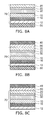
- FIG. 8A to FIG. 8C are schematic cross-sectional views showing processes for fabricating the semiconductor light emitting device structure shown in FIG. 5 ;
- FIG. 9A to FIG. 9D are schematic cross-sectional views showing processes for fabricating the semiconductor light emitting device structure shown in FIG. 5 ;
- FIG. 10A to FIG. 10F are schematic cross-sectional views showing processes for fabricating the semiconductor light emitting device structure shown in FIG. 5 .
- a semiconductor light emitting device includes: a first semiconductor layer of a first conductivity type; a second semiconductor layer of a second conductivity type; a light emitting layer; a conductive metal layer; and a first stress application layer.
- the first semiconductor layer contains a nitride semiconductor crystal and receives tensile stress in a (0001) plane.
- the second semiconductor layer contains a nitride semiconductor crystal.
- the light emitting layer is provided between the first semiconductor layer and the second semiconductor layer and contains a nitride semiconductor crystal.
- the light emitting layer has an average lattice constant larger than a lattice constant of the first semiconductor layer.
- the conductive metal layer is provided on an opposite side from the light emitting layer, on the second semiconductor layer.
- the conductive metal layer has a thermal expansion coefficient larger than a thermal expansion coefficient of a nitride semiconductor crystal.
- the conductive metal layer supports the first semiconductor layer, the light emitting layer, and the second semiconductor layer.
- the first stress application layer is provided between the second semiconductor layer and the light emitting layer. The first stress application layer relaxes tensile stress applied from the metal layer to the second semiconductor layer.
- FIG. 1 is a schematic cross-sectional view illustrating the configuration of a semiconductor light emitting device according to an embodiment.
- a semiconductor light emitting device 110 includes a first semiconductor layer 10 of a first conductivity type, a second semiconductor layer 20 of a second conductivity type, a light emitting layer 30 , a first stress application layer 22 , and a support substrate (a metal layer) 40 .
- the semiconductor light emitting device 110 is, for example, an LED device.
- the semiconductor light emitting device 110 may be also a laser diode. In the following, a description is given using the case where the semiconductor light emitting device 110 is an LED.
- An n-type semiconductor layer for example, is used as the first semiconductor layer 10 .
- a p-type semiconductor layer for example, is used as the second semiconductor layer 20 .
- the first semiconductor layer 10 may be the p type and the second semiconductor layer 20 may be the n type.
- a description is given using the case where the first semiconductor layer 10 is the n type and the second semiconductor layer 20 is the p type.
- the first semiconductor layer 10 and the second semiconductor layer 20 contain a nitride semiconductor crystal.
- the first semiconductor layer 10 inherently has tensile strain (elastic expansion and contraction of the lattice spacing resulting from receiving stress) in the in-plane direction due to the stress applied from the outside (e.g. the static force applied to the crystal). That is, due to tensile stress being applied to the first semiconductor layer 10 in the in-plane direction, the lattice length (the lattice spacing in the actual crystal lattice) in the in-plane direction of the first semiconductor layer 10 has been made longer than the original lattice constant (the value determined as a physical constant) of the first semiconductor layer 10 .
- the first semiconductor layer 10 is, for example, an n-type GaN layer.
- the second semiconductor layer 20 is, for example, a p-type GaN layer.
- the first semiconductor layer 10 may include, for example, an i-GaN layer (hereinafter, also referred to as a “non-doped GaN layer”) and an n-type GaN layer.
- the n-type GaN layer is laminated between the i-GaN layer and the second semiconductor layer 20 .
- the light emitting layer 30 is provided between the first semiconductor layer 10 and the second semiconductor layer 20 .
- the light emitting layer 30 contains a nitride semiconductor crystal.
- the light emitting layer 30 contains a nitride semiconductor crystal having a lattice constant still larger than the lattice length in the in-plane direction of the first semiconductor layer 10 that has been expanded in the in-plane direction by receiving tensile stress.
- the light emitting layer 30 includes, for example, a plurality of barrier layers 34 and a well layer 32 provided between barrier layers 34 .
- the well layer 32 may be provided in plural.
- the light emitting layer 30 has an MQW (multiple quantum well) structure.
- the well layer 32 and the barrier layer 34 contain a nitride semiconductor crystal.
- the well layer 32 contains a nitride semiconductor crystal having a lattice constant still larger than the lattice length in the in-plane direction of the first semiconductor layer 10 that has been expanded in the in-plane direction by receiving tensile stress.
- the lattice in the in-plane direction of the well layer 32 includes compressive strain (elastic expansion and contraction of the lattice spacing) and has a lattice length smaller than the original lattice constant in the in-plane direction of the well layer 32 , as a result of receiving compressive stress from the lattice of the first semiconductor layer 10 having a lattice length smaller than the lattice constant of the well layer 32 .
- the average lattice constant in the light emitting layer 30 is the lattice constant obtained by weighting by thickness distribution and averaging the lattice constant of the barrier layer 34 and the lattice constant of the well layer 32 .
- the average lattice constant of the light emitting layer 30 is larger than the lattice constant of the first semiconductor layer 10 .
- the average lattice constant of the light emitting layer 30 is larger than the lattice length in the in-plane direction of the first semiconductor layer 10 that has been expanded in the in-plane direction by receiving tensile stress.
- the average lattice constant in the light emitting layer 30 may become larger from the first semiconductor layer 10 toward the second semiconductor layer 20 in the light emitting layer 30 .
- the thicknesses of the plurality of well layers 32 in the light emitting layer 30 having an MQW structure may become thicker from the first semiconductor layer 10 toward the second semiconductor layer 20 .
- the first stress application layer 22 is provided between the second semiconductor layer 20 and the light emitting layer 30 .
- the first stress application layer 22 contains a nitride semiconductor crystal.
- the lattice constant of the first stress application layer 22 is smaller than the lattice constant of the first semiconductor layer 10 .
- the first stress application layer 22 relaxes the tensile stress applied from the support substrate 40 .
- the support substrate 40 is provided on one surface of the second semiconductor layer 20 , on the opposite side to the light emitting layer 30 .
- the support substrate 40 is a conductive metal layer.
- a metal such as copper, for example, is used for the support substrate 40 .
- At least one of a reflection metal 90 and a bonding metal may be interposed between the support substrate 40 and the second semiconductor layer 20 .
- the reflection metal 90 is interposed between the support substrate 40 and the second semiconductor layer 20 .
- the semiconductor light emitting device 110 may further include a second stress application layer 16 (see FIG. 5 ).
- the second stress application layer 16 is provided on the opposite side to the light emitting layer 30 from the first semiconductor layer 10 .
- the second stress application layer 16 contact with the first semiconductor layer 10 .
- the second stress application layer 16 applies compressive stress to the first semiconductor layer 10 , and thereby relaxes the tensile stress applied from the support substrate 40 . The stress is described later.
- the semiconductor light emitting device 110 further includes a first electrode 81 , a second electrode 82 , and the reflection metal 90 .
- the support substrate 40 containing a metal such as copper is bonded to the LED stacked structure including the second semiconductor layer 20 , the light emitting layer 30 , and the first semiconductor layer 10 via the reflection metal 90 containing Ag on the second semiconductor layer 20 side and a bonding metal containing AuSn.
- the light emitted from the light emitting layer 30 is emitted from the major surface (light extraction surface) on the first semiconductor layer 10 side.
- the major surface on the first semiconductor layer 10 side forms a light extraction surface.
- the light extraction surface may have undergone roughening processing.
- the LED stacked structure of nitride semiconductor crystals is formed between the second semiconductor layer 20 and the light extraction surface.
- the first semiconductor layer 10 is made of, for example, an n-type gallium nitride (GaN) crystal.
- the light emitting layer 30 formed of a multiple-layer film of the well layer 32 and the barrier layer 34 is stacked on the first semiconductor layer 10 .
- InGaN, for example, is used for the well layer 32 .
- GaN, for example, is used for the barrier layer 34 .
- the second semiconductor layer 20 is stacked on the quantum well structure of nitride semiconductors that forms the light emitting layer 30 .
- the second semiconductor layer 20 is made of, for example, a p-type gallium nitride crystal.
- stack includes not only the state where a plurality of layers are stacked in contact with one another but also the case where a plurality of layers are stacked via other layers.
- being provided “on” includes not only the case where an upper layer is provided in contact with a lower layer but also the case where an upper layer is provided on a lower layer via another layer.
- the lattice constant of the well layer 32 (e.g. an InGaN crystal layer) included in the light emitting layer 30 is larger than the lattice constant of the first semiconductor layer 10 (e.g. gallium nitride).
- the semiconductor light emitting device 110 has a structure in which a first nitride semiconductor crystal (e.g. the GaN crystal that forms the first semiconductor layer 10 and the second semiconductor layer 20 ) is used as matrices and a second nitride semiconductor crystal (the InGaN layer that forms the well layer 32 ) having a lattice constant larger than the lattice constant of the first nitride semiconductor crystal is placed between the matrices.
- a first nitride semiconductor crystal e.g. the GaN crystal that forms the first semiconductor layer 10 and the second semiconductor layer 20
- a second nitride semiconductor crystal the InGaN layer that forms the well layer 32
- the a-axis length (the lattice length in the a-axis direction) of the lattice of the first semiconductor crystal layer is longer than the intrinsic a-axis length (the lattice constant in the a-axis direction) of the GaN crystal. That is, the first semiconductor crystal layer has tensile stress (elastic expansion and contraction of the lattice spacing) in the a-axis direction, as a result of the inherent tensile stress from the outside being applied.
- the average lattice constant in the a-axis direction of the lattice of the light emitting layer 30 is longer than the a-axis length of the lattice of the first semiconductor crystal.
- the average lattice constant in the a-axis direction of the lattice in the light emitting layer 30 may become larger from the first semiconductor layer 10 toward the second semiconductor layer 20 in the light emitting layer 30 .
- the thicknesses of the plurality of well layers 32 in the light emitting layer 30 may become thicker from the first semiconductor layer 10 toward the second semiconductor layer 20 .
- the magnitude of the tensile stress applied to the GaN layer can be investigated by Raman spectroscopy as described later.
- the support substrate 40 is provided on the opposite side to the light emitting layer 30 , on the second semiconductor layer 20 .
- the support substrate 40 may be formed of copper or a metal containing copper.
- the thermal conductivity of the support substrate 40 is higher than the thermal conductivity of the nitride semiconductor crystal including the first semiconductor layer 10 , the second semiconductor layer 20 , and the light emitting layer 30 .
- the thermal expansion coefficient of the support substrate 40 is larger than the thermal expansion coefficient of the nitride semiconductor crystal including the first semiconductor layer 10 , the second semiconductor layer 20 , and the light emitting layer 30 .
- FIG. 2A and FIG. 2B are schematic cross-sectional views showing the stress generated in stacked structures.
- FIG. 3A and FIG. 3B are schematic cross-sectional views showing the stress generated in stacked structures including the support substrate.
- FIG. 4A and FIG. 4B are graphs showing the Raman spectra of gallium nitride crystals.
- FIG. 2A and FIG. 3A illustrate the stress generated in the LED stacked structure of the semiconductor light emitting device according to the embodiment.
- FIG. 2B and FIG. 3B illustrate the stress generated in the LED stacked structure of a semiconductor light emitting device of a reference example.
- FIG. 4A is a graph showing the Raman spectrum of a gallium nitride crystal and a silicon crystal.
- FIG. 4B is a graph showing a comparison between the Raman spectrum of a nitride semiconductor crystal grown on a silicon substrate and the Raman spectrum of a nitride semiconductor crystal grown on a sapphire substrate.
- the vertical axis of FIG. 4A and FIG. 4B represents the intensity I (an arbitrary unit).
- the horizontal axis of FIG. 4A and FIG. 4B represents the wave number RS (cm ⁇ 1 ).
- a gallium nitride crystal layer with a surface of the (0001) plane is formed on a sapphire substrate 55 having a surface of the (0001) plane, and further the light emitting layer 30 including an InGaN thin-film crystal layer is combined.
- Each semiconductor crystal of the semiconductor light emitting device 119 a of the reference example formed on the sapphire substrate 55 with a surface of the (0001) plane is oriented in the c-axis direction.
- a light emitting diode in which nitride semiconductor crystal layers are stacked on the sapphire substrate 55 like the semiconductor light emitting device 119 a has a structure in which an n-type GaN layer (the first semiconductor layer 10 ), a quantum well light emitting layer (the light emitting layer 30 ), and a p-type GaN layer (the second semiconductor layer 20 ) are stacked on the sapphire substrate 55 .
- the sapphire substrate 55 is almost transparent to the wavelength band of the blue color region.
- a structure is employed in which a reflection film 57 is formed on the back surface of the sapphire substrate 55 and light is thereby extracted from the upper portion of the p-type GaN layer on the front surface side (the face-up structure).
- the equivalent lattice length of the sapphire crystal serving for the lattice for the epitaxial growth of gallium nitride is smaller than the lattice constant of gallium nitride.
- the thermal expansion coefficient of the gallium nitride crystal is smaller than the thermal expansion coefficient of the sapphire crystal serving as the underlayer. Therefore, as illustrated by arrow A 1 and arrow A 2 shown in FIG. 2B , a large compressive stress is applied to the gallium nitride crystal layer when thin-film crystal growth at high temperature has been completed and the temperature has been lowered to room temperature.
- the gallium nitride crystal layer has compressive strain (elastic expansion and contraction of the lattice spacing). That is, the lattice length in the a-axis direction of the gallium nitride crystal layer epitaxially grown on the sapphire substrate 55 is shorter than the original lattice constant in the a-axis direction of the gallium nitride crystal.
- the lattice constant of the InGaN crystal layer included in the light emitting layer 30 is larger than the lattice constant of gallium nitride. Therefore, as illustrated by arrow A 3 and arrow A 4 shown in FIG. 2B , stress in the drawing direction (tensile stress) is applied from the InGaN crystal layer to the gallium nitride crystal layer to which the compressive stress from the sapphire crystal has been applied. On the other hand, as illustrated by arrow A 5 and arrow A 6 shown in FIG. 2B , the light emitting layer 30 receives compressive stress from the gallium nitride crystal layer. Such compressive stress and tensile stress are, in other words, generated in the a-axis direction in the (0001) plane, for example.
- the tensile stress applied to the gallium nitride crystal layer from the InGaN crystal layer having a lattice constant larger than the lattice constant of gallium nitride is relatively balanced with the compressive stress applied to the gallium nitride layer from the sapphire crystal. Therefore, there are few cases where defects are generated from the end surface of the n-type GaN layer, or the end surface of the p-type GaN layer, etc.
- a structure is employed in which an LED structure made of nitride semiconductors is epitaxially grown on the sapphire substrate 55 , then the surface side of the p-type GaN layer is attached to the support substrate 40 with a high thermal conductivity, and the sapphire substrate 55 is peeled off (the thin-film structure).
- a metal such as copper may be used as the support substrate 40 .
- the thermal expansion coefficient of a metal such as copper is generally larger than the thermal expansion coefficient of the nitride semiconductor crystal including the first semiconductor layer 10 , the second semiconductor layer 20 , and the light emitting layer 30 .
- the thermal expansion coefficient of gallium nitride is 5.6 ⁇ 10 ⁇ 6 K ⁇ 1 .
- the thermal expansion coefficient of copper is 16.8 ⁇ 10 ⁇ 6 K ⁇ 1 . That is, when the LED device of the thin-film structure using copper as the support substrate 40 is operated at high temperature, the support substrate 40 expands more than the nitride semiconductor crystal layer, as illustrated by arrow A 7 and arrow A 8 shown in FIG. 3B . Consequently, the nitride semiconductor crystal layer receives tensile stress from the support substrate 40 .
- the findings by the inventors have revealed that the compressive strain due to the compressive stress applied to the gallium nitride crystal layer from the sapphire substrate 55 remains also in the thin-film structure from which the sapphire substrate 55 has been removed. That is, even after the sapphire substrate 55 is removed, the lattice length in the a-axis direction of the gallium nitride crystal layer is shorter than the original lattice constant in the a-axis direction of the gallium nitride crystal.
- the compressive strain (elastic expansion and contraction of the lattice spacing resulting from receiving stress) that has remained in the interior of crystal is balanced also when the tensile stress from the support substrate 40 is applied in high temperature operation. Consequently, withstanding properties against the crack formation by the stress are high.
- the semiconductor light emitting device 110 has an LED stacked structure that is formed on a silicon crystal with a surface of the (111) plane and includes an n-type GaN layer (the first semiconductor layer 10 ), a quantum well light emitting layer (the light emitting layer 30 ), and a p-type GaN layer (the second semiconductor layer 20 ) stacked.
- Each semiconductor crystal of the semiconductor light emitting device 110 formed on a silicon substrate 50 with a surface of the (111) plane is oriented in the c-axis direction.
- the equivalent lattice length of the silicon crystal with a surface of the (111) plane for the lattice of epitaxial growth of gallium nitride is larger than the lattice constant in the a-axis direction of gallium nitride.
- the thermal expansion coefficient of the silicon crystal is smaller than the thermal expansion coefficient of gallium nitride. Therefore, as illustrated by arrow A 11 and arrow A 12 shown in FIG. 2A , a strong tensile stress is applied to the gallium nitride crystal layer after crystal growth is finished.
- the gallium nitride crystal layer has tensile strain (elastic expansion and contraction of the lattice spacing). Furthermore, as illustrated by arrow A 13 and arrow A 14 shown in FIG.
- the nitride semiconductor crystal system formed on the silicon crystal receives further tensile stress from the InGaN crystal layer.
- the light emitting layer 30 receives compressive stress from the gallium nitride crystal layer.
- Such compressive stress and tensile stress are, in other words, generated in the a-axis direction in the (0001) plane, for example.
- the tensile stress applied to the gallium nitride crystal layer from the InGaN crystal layer having a lattice constant larger than the lattice constant of gallium nitride synergizes with the tensile stress applied to the gallium nitride crystal layer from the silicon crystal. Therefore, in the case where a nitride semiconductor crystal is epitaxially grown on the silicon substrate 50 to form a semiconductor light emitting device, the tensile stress accumulated in the epitaxial crystal layer may not only cause elastic deformation (strain) of the crystal lattice but also generate cracks, defects, etc. as plastic deformation of the crystal. Consequently, obstruction may be caused in device fabrication processes and device operation, or the device characteristics may be degraded.
- the silicon substrate 50 is generally not transparent to the wavelength of the light used.
- the thin-film structure is employed in which the grown layer is peeled off from the silicon substrate.
- a metal such as copper and aluminum may be used as the support substrate 40 .
- the thermal expansion coefficient of a metal having a high thermal conductivity, such as copper and aluminum is generally larger than the thermal expansion coefficient of the nitride semiconductor crystal.
- the tensile stress (elastic expansion and contraction of the lattice spacing) generated by the stress that is accumulated in the nitride semiconductor crystal layer after the growth due to the difference between the lattice constant of the substrate and the lattice constant of the crystal layer or the difference between the thermal expansion coefficient of the substrate and the thermal expansion coefficient of the crystal layer remains even after the growth substrate is peeled off.
- the nitride semiconductor crystal layer receives not only the tensile stress that has remained in the interior of crystal, but also the tensile stress resulting from the difference between the thermal expansion coefficient of the support substrate 40 and the thermal expansion coefficient of the crystal layer. That is, in the case where an LED structure made of nitride semiconductor crystals is grown on the Si substrate 50 , tensile strain (elastic expansion and contraction of the lattice spacing) is included in the GaN crystal layer.
- the lattice length in the a-axis direction of the GaN crystal is larger than the original lattice constant in the a-axis direction of the GaN crystal.
- the support substrate 40 formed of a metal such as copper in the thin-film structure, in high temperature operation, the tensile stress resulting from the difference between the thermal expansion coefficient of the support substrate 40 and the thermal expansion coefficient of the crystal layer works synergistically with the tensile strain included in the crystal layer. Thereby, the risk of plastic deformation such as defects and cracks will be caused is increased in high temperature operation, and it results in characteristic degradation and device operational malfunction.
- the In composition ratio of the light emitting layer 30 is high and the average lattice length of the light emitting layer 30 is large, the tensile stress applied from the InGaN crystal layer to the gallium nitride crystal layer is large, and malfunction occurring in operation is significant. Also when the thickness of the InGaN crystal layer is thick, malfunction occurring in operation is significant.
- the average lattice constant in the light emitting layer 30 becomes larger from the first semiconductor layer 10 toward the second semiconductor layer 20 . Therefore, in the case where tensile stress is applied from the support substrate 40 to the second semiconductor layer 20 , the risk of the formation of crystal defects and cracks is further increased. Specifically, in the case where the thicknesses of the plurality of InGaN well layers 32 in the light emitting layer 30 become thicker from the first semiconductor layer 10 toward the second semiconductor layer 20 , a larger tensile stress is effectively applied to the second semiconductor layer 20 . Thus, the tensile stress applied from the support substrate 40 works more synergistically.
- the first stress application layer 22 is provided between the second semiconductor layer 20 and the light emitting layer 30 .
- the first stress application layer 22 relaxes the tensile stress applied from the support substrate 40 .
- the first stress application layer 22 includes, for example, an AlGaN layer.
- the first stress application layer 22 is not limited to including one AlGaN layer but may include a plurality of AlGaN layers.
- the first stress application layer 22 can relax the tensile stress applied from the support substrate 40 even under conditions where tensile strain remains in the first semiconductor crystal. Therefore, the formation of cracks or the introduction of defects in high temperature operation can be suppressed, and a semiconductor light emitting device with high light emission efficiency can be provided. Specifically, in the case where the support substrate 40 formed of a metal such as copper is used in the thin-film structure, even when tensile stress is generated in operation at high current density (in high temperature operation), the formation of cracks or the introduction of defects can be suppressed, and a semiconductor light emitting device with high light emission efficiency can be provided.
- the support substrate 40 that applies tensile stress is further included in the thin-film crystal having tensile stress (the first semiconductor layer 10 )
- the first stress application layer 22 for relaxing the tensile stress applied from the support substrate 40 is laminated. Therefore, the degradation in device characteristics resulting from the introduction of defects due to tensile stress can be suppressed.
- the stress applied to the gallium nitride crystal layer is compressive stress or tensile stress can be determined from a Raman spectrum.
- the peak of the Raman spectrum of a gallium nitride crystal to which no stress is applied is at approximately 568 cm ⁇ 1
- the peak appears at a wave number RS larger than 568 cm ⁇ 1 , up to approximately 575 cm ⁇ 1 , in a gallium nitride crystal to which compressive stress is applied.
- a tensile stress of 0.1 to 0.15% is included in a GaN crystal layer grown on the silicon substrate 50 .
- FIG. 5 is a schematic cross-sectional view showing an example of the crystal stacked structure when a semiconductor light emitting device according to the embodiment is fabricated.
- a buffer layer 12 (a layer that can form a second stress application layer described later) including an AlN layer and an AlGaN layer is laminated on the silicon substrate 50 .
- An AlN layer (which plays a stress controlling layer during growth, and is to be the second stress application layer in the device.) 16 with a thickness of 15 nanometers (nm) is provided on the buffer layer 12 via a non-doped GaN layer 14 with a thickness of 300 nm.
- the first semiconductor layer 10 is stacked on the AlN layer 16 .
- An n-type GaN layer 18 with a thickness of 2 micrometers ( ⁇ m) and a non-doped GaN layer 17 with a thickness of 1 ⁇ m are stacked in the first semiconductor layer 10 .
- the MQW light emitting layer 30 is stacked on the SLS layer 60 .
- the MQW light emitting layer 30 has a structure in which the barrier layer 34 with a thickness of 5 nm made of GaN and the well layer 32 formed of an InGaN layer with an In content of 15% and a thickness of 3 nm are formed repeatedly 8 times.
- the composition ratio of In in the well layer 32 is, for example, not less than 0.12 and not more than 0.20.
- a p-type AlGaN layer (the first stress application layer 22 ) with an Al content of 20% is laminated on the light emitting layer 30 .
- a p-type GaN layer (the second semiconductor layer 20 ) is laminated on the p-type AlGan layer (the first stress application layer 22 ).
- the reflection metal 90 is laminated on the p-type GaN layer (the second semiconductor layer 20 ).
- the support substrate 40 of copper is attached onto the reflection metal 90 via a bonding metal. After the support substrate 40 is attached in accordance with the processes described later and an n electrode is formed, the silicon substrate 50 for epitaxial growth is peeled off; thus, the process is completed.
- the second stress application layer 16 is interposed between the buffer layer 12 and the first semiconductor layer 10 (an n-type GaN layer). The second stress application layer 16 can be taken into the device by not removing but leaving the stress controlling layer during growth.
- the thermal expansion coefficient of gallium nitride is 5.6 ⁇ 10 ⁇ 6 K ⁇ 1 .
- the thermal expansion coefficient of copper is 16.8 ⁇ 10 ⁇ 6 K ⁇ 1 .
- a current of 350 mA or more is passed.
- the temperature in the device may reach approximately 100° C. to 200° C.
- the thermal expansion rate of gallium nitride is approximately 0.11%.
- the thermal expansion rate of copper, which is the support substrate 40 is approximately 0.33%.
- the thermal expansion rate of copper, which is the support substrate 40 is approximately three times the thermal expansion rate of gallium nitride. That is, a tensile stress equivalent to the difference of 0.22% is applied to the gallium nitride crystal layer.
- the lattice constant in the in-plane direction (the a-axis direction) of a GaN crystal is 0.518 nm.
- the lattice constant in the in-plane direction (the a-axis direction) of an AlN crystal is 0.498 nm.
- the difference between the lattice constant in the in-plane direction (the a-axis direction) of the GaN crystal and the lattice constant in the in-plane direction (the a-axis direction) of the AlN crystal is approximately 4%.
- an AlGaN crystal with an Al content of approximately 5% (the lattice constant in the a-axis direction being approximately 0.517 nm, the mismatch factor to the GaN crystal being 0.2%) is suitable as the first stress application layer 22 .
- the Al composition ratio of the AlGaN layer that forms the first stress application layer 22 may be as high as approximately 30%.
- the thickness of the first stress application layer 22 is set within a range of 5 to 20 nm.
- the second stress application layer 16 since it is away from the bonding interface between the support substrate 40 of copper including the reflection metal and the p-type GaN layer 20 via the light emitting layer 30 , an AlGaN layer with an Al content higher than the Al content of the first stress application layer 22 is suitable. That is, the lattice constant of the second stress application layer 16 is preferably smaller than the lattice constant of the first stress application layer 22 . Specifically, an AlN crystal layer is preferable. The thickness of the second stress application layer 16 is set to 10 to 50 nm. The second stress application layer 16 may have a two-layer structure of an AlN layer and an AlGaN layer with an Al content of approximately 50% or less.
- FIG. 6A and FIG. 6B are schematic diagrams showing the stress generated in another stacked structure.
- FIG. 6A is a schematic cross-sectional view showing the configuration of the other stacked structure.
- FIG. 6B is a graph showing an example of the relationship between the position in the stacking direction and the internal stress.
- the “stacking direction” refers to the direction from the first semiconductor layer 10 toward the second semiconductor layer 20 or the direction from the second semiconductor layer 20 toward the first semiconductor layer 10 .
- the thicknesses of the plurality of well layers 32 in the light emitting layer 30 having an MQW structure become thicker from the first semiconductor layer 10 toward the second semiconductor layer 20 .
- the thicknesses of the well layers 32 other than the well layer 32 nearest to the p-type GaN layer out of the plurality of well layers 32 is 3 nm.
- the thickness of the well layer 32 nearest to the p-type GaN layer is 5 nm.
- the thickness of the barrier layer 34 of the light emitting layer 30 is 5 nm. This is similar to the thickness of the barrier layer 34 of the semiconductor light emitting device 120 described above in regard to FIG. 5 .
- the tensile stress applied to the p-type GaN layer from the well layer 32 is relatively strong.
- the tensile stress applied to the p-type GaN layer from the well layer 32 is superposed with the tensile stress applied to the p-type GaN layer from the support substrate 40 of copper.
- the frequency of crack formation in high temperature operation is increased. Therefore, the effect of the first stress application layer 22 made of an AlGaN crystal is more significant.
- the average lattice constant becomes larger effectively from the n-type GaN layer (the first semiconductor layer 10 ) toward the p-type GaN layer (the second semiconductor layer 20 ) in the light emitting layer 30 , the effect of the first stress application layer 22 is larger.
- the difference between the lattice constant of the first stress application layer 22 (an AlGaN layer) and the lattice constant of the well layer 32 is large, and the risk is increased that defects will occur at the interface between the light emitting layer 30 and the first stress application layer 22 .
- FIG. 7 is a schematic cross-sectional view showing the stress generated in a still another stacked structure.
- a semiconductor light emitting device 140 similarly to the semiconductor light emitting device 130 described above in regard to FIG. 6A and FIG. 6B , the thicknesses of the plurality of well layers 32 in the light emitting layer 30 having an MQW structure become thicker from the first semiconductor layer 10 toward the second semiconductor layer 20 .
- making the interior of the first stress application layer 22 to be a two-layer structure is one effective means. That is, an AlGaN layer with a relatively low Al content is used as a first stress application unit 22 a on the side near to the light emitting layer 30 . An AlGaN layer with a relatively high Al content is used as a second stress application unit 22 b on the side near to the p-type GaN layer (the second semiconductor layer 20 ). Specifically, for example, the first stress application unit 22 a on the side near to the light emitting layer 30 is formed to be an AlGaN layer with an Al content of 10% and a thickness of 10 nm.
- the second stress application unit 22 b thereon on the side near to the p-type GaN layer is stacked to be an AlGaN layer with an Al content of 20% and a thickness of 10 nm.
- the structure of the first stress application layer 22 is not limited to a two-layer structure of AlGaN layers.
- the first stress application layer 22 may have a multiple-layer structure of three or more layers, or may have a structure with a continuously gradient composition ratio. A structure in which the lattice constant becomes smaller from the light emitting layer 30 toward the p-type GaN layer is more preferable.
- FIG. 8A to FIG. 10F are schematic cross-sectional views showing processes for fabricating the semiconductor light emitting device structure shown in FIG. 5 .
- the silicon substrate 50 with a surface of the (111) plane is prepared as a substrate for the crystal growth of a thin-film nitride semiconductor.
- the thickness of the crystal of the silicon substrate 50 is, for example, approximately 525 ⁇ m.
- the thickness of the crystal of the silicon substrate 50 is not limited thereto, and may be, for example, approximately 250 ⁇ m to 1000 ⁇ m.
- the surface of the Si substrate 50 placed in the air is coated with a native oxide.
- a native oxide To epitaxially grow a nitride semiconductor crystal layer, it is necessary to remove the native oxide and reveal the silicon crystal surface.
- hydrofluoric acid treatment is performed on the silicon substrate 50 in order to perform hydrogen termination, which is a means to reveal the silicon crystal surface at relatively low temperature.
- the silicon substrate 50 is treated with a dilute hydrofluoric acid solution with a concentration of approximately 1% for about 1 minute. By this treatment, the surface of the Si layer becomes a hydrogen-terminated surface structure, which is a water-repellent surface.
- the hydrogen atoms covering the silicon crystal surface desorbs at a temperature of approximately 700° C. Thereby, a clean silicon crystal surface can be obtained.
- a silicon crystal substrate with the surface covered with a thin native oxide is heat-treated at a high temperature of 1000° C. or more.
- the Si substrate 50 of which the surface has been hydrogen-terminated is introduced into a film deposition apparatus (an MOCVD apparatus) using an organic metal and ammonia gas as the source material, and an AlN layer with a thickness of 100 nm is stacked at a film deposition temperature of 1200° C.
- a film deposition apparatus an MOCVD apparatus
- an organic metal and ammonia gas as the source material
- an AlN layer with a thickness of 100 nm is stacked at a film deposition temperature of 1200° C.
- an MOCVD apparatus an MOCVD apparatus
- the selection of the film deposition method is arbitrary.
- an ECR plasma sputtering apparatus, an MBE apparatus, etc. may be used as the film deposition apparatus of the AlN layer.
- the film deposition of the AlN layer on the Si substrate 50 is performed by other than an MOCVD apparatus, after the film deposition of the AlN layer, the substrate is introduced into an MOCVD apparatus, and subsequently the film deposition processes below are performed.
- the substrate temperature is set to 1100° C. to stack an AlGaN layer with an Al content of 25% and a thickness of 250 nm.
- the AlN layer and the AlGaN layer thus formed correspond to the buffer layer 12 shown in FIG. 5 .
- a gallium nitride layer of 0.3 to 1.0 ⁇ m is formed using TMG (trimethylgallium) and NH 3 (ammonia) as the source material.
- TMG trimethylgallium
- NH 3 ammonia
- the film deposition temperature is lowered to 700° C. to grow an AlN layer 16 with a thickness of 15 nm.
- the AlN layer 16 functions as a stress controlling layer during growth.
- an AlGaN layer with a thickness of 50 nm and an Al content of 25% may be further stacked on the AlN layer 16 .
- the AlN layer 16 or the stacked structure of the AlN layer 16 and the AlGaN layer may be used as the second stress application layer.
- the AlN layer 16 with a thickness of 15 nm serving as a stress controlling layer during growth may not be interposed, and an AlN layer that forms the buffer layer 12 (alternatively, the buffer layer 12 formed of a stacked structure of an AlN layer and an AlGaN layer) may be used as the second stress application layer.
- an n-type GaN (the first semiconductor layer) 10 is stacked.
- Si is adoped as an impurity with a concentration of 1 ⁇ 10 19 cm ⁇ 2 .
- the n-type GaN 10 may not be formed directly on the AlN layer 16 , but a intermediate layer (non-doped barrier layer) 17 containing no impurity may be grown with a thickness of approximately 1 to 3 ⁇ m and then an n-type GaN layer 18 may be stacked.
- the first semiconductor layer 10 may have a structure in which the non-doped GaN layer 17 and the n-type GaN layer 18 are stacked.
- the SLS layer 60 formed of a multiple-layer film of InGaN and GaN and the light emitting layer (MQW light emitting layer) 30 are stacked on the n-type gallium nitride crystal layer 10 .
- the upper portion of the crystal structure is doped with a p-type impurity (Mg).
- Mg p-type impurity
- an AlGaN layer (the first stress application layer 22 ) with an Al content of 20% and a thickness of 150 nm and p-type GaN (the second semiconductor layer 20 ) not containing Al are formed on the light emitting layer 30 .
- the AlGaN layer may be doped with a p-type impurity (Mg).
- Mg p-type impurity
- the doping concentration of Mg is preferably a concentration in a range of 1 ⁇ 10 19 to 1 ⁇ 10 20 cm ⁇ 2 .
- the doping concentration changes due to the memory effect; therefore, a uniform doping profile is not necessarily obtained.
- the doping concentration of Mg is allowed to deviate from the range described above.
- the chemical vapor deposition method (the MOCVD method) using an organic metal is given as the method for the thin-film crystal growth of the n-type GaN crystal layer 10 , the light emitting layer 30 , the first stress application layer 22 , and the p-type GaN 20
- the method is not limited thereto.
- any method such as the molecular beam epitaxy (MBE) method and the hydride vapor phase epitaxy (HVPE) method, which are thin-film crystal growth methods commonly used for nitride semiconductor crystal growth, may be used.
- a thin-film crystal layer (a crystal growth layer) 70 of an LED structure can be epitaxially grown.
- a metal film (the reflection metal 90 ) containing Ag functioning as both a reflection film and a contact layer, for example a silver nickel layer is stacked on the surface of the second semiconductor layer 20 , and then the workpiece is attached to the conductive support substrate 40 of copper or the like via a bonding metal (e.g. a gold-tin alloy (not shown)), with an intermediate layer (not shown) made of a metal material such as Ti, W, Pt, and Au interposed therebetween.
- the thickness of the support substrate 40 is preferably approximately 100 to 200 ⁇ m.
- An electrode is formed on the reflection metal 90 (or a bonding metal further stacked, or the support substrate 40 ); thereby, a p-side electrode can be formed.
- the Si substrate 50 which is a substrate for thin-film crystal growth, is removed.
- the support substrate 40 is attached to the second semiconductor layer 20 side, and then the growth substrate is ground; thereby, the Si substrate 50 for growth can be removed.
- the small amount of residual Si is removed by dry etching using SF 6 gas as an etchant; thereby, the AlN layer (the buffer layer 12 ) formed on the Si substrate 50 at the beginning can be revealed.
- the AlN layer has the property of increasing the amount of resistance components. Therefore, for example in a semiconductor light emitting device having the stacked structure described above in regard to FIG. 5 , there is an example in which the AlN-based buffer layer (e.g. the buffer layer 12 including an AlN layer) and the AlN-based stress controlling layer during growth are removed to reveal the n-type GaN layer 18 and then an n-side electrode is provided.
- the AlN-based buffer layer e.g. the buffer layer 12 including an AlN layer
- the AlN-based stress controlling layer during growth are removed to reveal the n-type GaN layer 18 and then an n-side electrode is provided.
- the AlN-based buffer layer or the AlN layer has a high contact resistance.
- the amount of series resistance components is increased. Therefore, in common processes, the AlN-based buffer layer and the AlN-based stress controlling layer during growth in the electrode formation portion are removed to reveal the n-type GaN layer in the portion where the n-side electrode (the first electrode 81 ) will be formed.
- the crystal growth layer 70 is divided with the size of the device.
- the substrate side below the metal of a p-type electrode (the second electrode 82 ) is kept in the state of not being divided.
- portions other than the portion where an n-side electrode (the first electrode 81 ) will be formed are protected by a mask 87 , and the portion from the buffer layer 12 to the stress controlling layer during growth is removed by etching to reveal the first semiconductor layer 10 (n-type GaN).
- the n-side electrode (the first electrode 81 ) is protected by a mask 89 , and a KOH solution is used to perform roughening processing with a depth of approximately 500 nm on the nitride semiconductor surface (the first semiconductor layer 10 ) side.
- the AlN and the AlGaN layer (the buffer layer 12 ) revealed at the surface are removed by etching.
- the AlN-based stress controlling layer during growth included in the crystal growth layer 70 (the nitride semiconductor crystal layer unit 70 a ) is removed by the roughening processing of the nitride semiconductor surface.
- the AlN-based stress controlling layer during growth may not be removed but be used as the second stress application layer (see FIG. 9C ).
- a p-type electrode and an n-type electrode are formed to complete the fabrication.
- the process of epitaxial growth of a stacked structure of a nitride semiconductor thin-film crystal having an LED structure on the silicon substrate 50 with a surface of the (111) plane is similar to the above, and a description is therefore omitted.
- a protection film 85 is formed on the entire surface of the p-type GaN layer. After that, an opening is partly provided, and etching processing is performed.
- the p-type layer, the first stress application layer 22 , and the light emitting layer 30 in the opening portion are etched to reveal the n-GaN layer 10 (see FIG. 10A ).
- an ohmic contact 83 made of Ti, Al, Ni, Au, or the like is formed on the revealed portion of the n-GaN layer.
- the protection film 85 covering the p-type GaN layer is removed, and a protection film 84 is formed on the n electrode formation portion.
- the reflection metal 90 made of silver or an alloy containing silver as a main component is stacked on the surface of the p-type GaN layer.
- an intermediate layer (not shown) made of a metal such as, for example, Ti, W, Au, Pt, and Al is interposed and further a bonding metal (not shown) made of a gold-tin alloy is stacked.
- the support substrate 40 made of a metal such as copper is attached (see FIG. 10C ).
- the thickness of the support substrate is preferably approximately 100 to 200 ⁇ m.
- the Si substrate 50 used for the epitaxial growth is peeled off to reveal the AlN buffer layer 12 .
- the AlN buffer layer is revealed, roughening processing is performed on the revealed surface.
- the AlN buffer layer is removed.
- the AlN-based stress controlling layer during growth is removed.
- the AlN-based stress controlling layer during growth is not removed but used as the second stress application layer 16 (see FIG. 10E ).
- the n electrode portion of the support substrate 40 of copper is opened. Subsequently, an n extension electrode, which is insulated from the support substrate 40 , is revealed and an interconnection of the n electrode is connected.
- the substrate 40 can be used as a p-side electrode (see FIG. 10F ).
- the support substrate 40 of copper is attached onto the flat p-GaN layer.
- the support substrate 40 of copper is attached onto the p-type GaN layer in which the n electrode portion is formed beforehand. That is, it is necessary to attach the support substrate 40 of copper to a surface partly having the unevenness caused by processing (not flat).
- a bonding metal layer is interposed to follow the unevenness of the bonding surface.
- degradation in bonding conditions due to the formation of voids etc. is likely to occur as compared to attachment to a flat surface.
- a method in which the support substrate 40 of copper is formed by a plating process, not attaching it as a plate-like substrate as described above is one effective means.
- the preliminary processing of the formation of an n electrode and a p electrode is performed on a substrate in which a nitride semiconductor crystal layer of an LED structure is epitaxially grown on the silicon substrate 50 .
- the reflection metal 90 made of silver or containing silver as a main component and an intermediate layer made of a metal such as Ti, W, and Pt are stacked by the chemical vapor deposition method, the sputtering method, or the like.
- a seed layer containing Ti and Cu is stacked, and finally the plating method is used to form copper with a thickness of approximately 100 ⁇ m.
- the support substrate 40 of copper is formed by the plating method, a structure with high adhesion to the unevenness of the electrode formation portion can be fabricated.
- the material of the conductive support substrate 40 may be, in addition to copper (thermal conductivity: 370 to 380 Wm ⁇ 1 K ⁇ 1 , thermal expansion coefficient: 16.6 ⁇ 10 ⁇ 6 K ⁇ 1 ), gold (thermal conductivity: 295 to 320 Wm ⁇ 1 K ⁇ 1 , thermal expansion coefficient: 14.2 ⁇ 10 ⁇ 6 K ⁇ 1 ), silver (thermal conductivity: 418 Wm ⁇ 1 K ⁇ 1 , thermal expansion coefficient: 18.9 ⁇ 10 ⁇ 6 K ⁇ 1 ), or the like.
- the material of the conductive support substrate 40 may be also aluminum (thermal conductivity: 200 to 230 Wm ⁇ 1 K ⁇ 1 , thermal expansion coefficient: 23.1 ⁇ 10 ⁇ 6 K ⁇ 1 ).
- the material of the conductive support substrate 40 may be also an alloy of two or more of the metals mentioned above, an alloy using any of the metals mentioned above as a matrix, or the like.
- the conductive support substrate 40 may have a stacked film structure in which a layer of any of the metals, including alloys, mentioned above is used as a main layer and is combined with another material. That is, the support substrate 40 of the embodiment contains a metal selected from the group consisting of gold (Au), silver (Ag), copper (Cu), and aluminum (Al) or an alloy containing two or more selected from the group mentioned above.
- nitride semiconductor includes all semiconductors expressed by the chemical formula of B x In y Al z Ga 1-x-y-z N (0 ⁇ x ⁇ 1, 0 ⁇ y ⁇ 1, 0 ⁇ z ⁇ 1, x+y+z ⁇ 1) in which the composition ratios x, y, and z are changed in the respective ranges. Furthermore, in the chemical formula mentioned above, also those further containing a group V device other than N (nitrogen), those further containing various devices added in order to control various properties such as the conductivity type, and those further containing various devices unintentionally contained are included in the “nitride semiconductor.”
Abstract
Description
Claims (26)
Applications Claiming Priority (2)
| Application Number | Priority Date | Filing Date | Title |
|---|---|---|---|
| JP2012256631A JP5460831B1 (en) | 2012-11-22 | 2012-11-22 | Semiconductor light emitting device |
| JP2012-256631 | 2012-11-22 |
Publications (2)
| Publication Number | Publication Date |
|---|---|
| US20140138614A1 US20140138614A1 (en) | 2014-05-22 |
| US9419175B2 true US9419175B2 (en) | 2016-08-16 |
Family
ID=50619310
Family Applications (1)
| Application Number | Title | Priority Date | Filing Date |
|---|---|---|---|
| US13/779,978 Active 2033-06-21 US9419175B2 (en) | 2012-11-22 | 2013-02-28 | Semiconductor light emitting device |
Country Status (2)
| Country | Link |
|---|---|
| US (1) | US9419175B2 (en) |
| JP (1) | JP5460831B1 (en) |
Families Citing this family (10)
| Publication number | Priority date | Publication date | Assignee | Title |
|---|---|---|---|---|
| JP5460831B1 (en) * | 2012-11-22 | 2014-04-02 | 株式会社東芝 | Semiconductor light emitting device |
| US8860005B1 (en) * | 2013-08-08 | 2014-10-14 | International Business Machines Corporation | Thin light emitting diode and fabrication method |
| JP2016171196A (en) * | 2015-03-12 | 2016-09-23 | 株式会社東芝 | Semiconductor device manufacturing method |
| US9865769B2 (en) | 2015-03-23 | 2018-01-09 | International Business Machines Corporation | Back contact LED through spalling |
| WO2017117151A1 (en) * | 2015-12-29 | 2017-07-06 | Light Share, LLC | Optoelectronic semiconductor devices with enhanced light output |
| US11322650B2 (en) | 2017-07-28 | 2022-05-03 | Lumileds Llc | Strained AlGaInP layers for efficient electron and hole blocking in light emitting devices |
| KR102294202B1 (en) * | 2017-07-28 | 2021-08-25 | 루미레즈 엘엘씨 | Modified AlGaInP Layers for Efficient Electron and Hole Blocking in Light Emitting Devices |
| US10141477B1 (en) * | 2017-07-28 | 2018-11-27 | Lumileds Llc | Strained AlGaInP layers for efficient electron and hole blocking in light emitting devices |
| CN113097353B (en) * | 2021-04-02 | 2022-07-15 | 厦门乾照光电股份有限公司 | Ultraviolet LED and manufacturing method thereof |
| US20230131918A1 (en) * | 2021-10-25 | 2023-04-27 | Meta Platforms Technologies, Llc | Strain management of iii-p micro-led epitaxy towards higher efficiency and low bow |
Citations (23)
| Publication number | Priority date | Publication date | Assignee | Title |
|---|---|---|---|---|
| JPH10145006A (en) | 1996-09-10 | 1998-05-29 | Toshiba Corp | Compound semiconductor device |
| US5777350A (en) * | 1994-12-02 | 1998-07-07 | Nichia Chemical Industries, Ltd. | Nitride semiconductor light-emitting device |
| US6100545A (en) * | 1997-10-10 | 2000-08-08 | Toyoda Gosei Co., Ltd. | GaN type semiconductor device |
| US20030132448A1 (en) * | 1999-01-07 | 2003-07-17 | Matsushita Electric Industrial Co., Ltd. | Semiconductor light-emitting device, method for fabricating the same and optical disk apparatus |
| US6597017B1 (en) * | 1999-03-26 | 2003-07-22 | Fuji Xerox Co., Ltd. | Semiconductor device, surface emitting semiconductor laser and edge emitting semiconductor laser |
| US6984840B2 (en) * | 1998-05-18 | 2006-01-10 | Fujitsu Limited | Optical semiconductor device having an epitaxial layer of III-V compound semiconductor material containing N as a group V element |
| US20070014324A1 (en) * | 2005-07-04 | 2007-01-18 | Osamu Maeda | Vertical cavity surface emitting laser |
| JP2007123878A (en) | 2005-10-25 | 2007-05-17 | Samsung Electro Mech Co Ltd | Nitride semiconductor light-emitting element |
| US20070121690A1 (en) * | 2003-12-09 | 2007-05-31 | Tetsuo Fujii | Highly efficient gallium nitride based light emitting diodes via surface roughening |
| US20090245310A1 (en) * | 2008-03-31 | 2009-10-01 | Sanyo Electric Co., Ltd. | Nitride-based semiconductor laser device and method of manufacturing the same |
| US20100265981A1 (en) * | 2007-12-21 | 2010-10-21 | Sanyo Electric Co., Ltd. | Nitride-based semiconductor light-emitting diode, nitride-based semiconductor laser device, method of manufacturing the same, and method of forming nitride-based semiconductor layer |
| JP2011166031A (en) | 2010-02-12 | 2011-08-25 | Toshiba Corp | Semiconductor light emitting element |
| JP2011233936A (en) | 2006-02-23 | 2011-11-17 | Azzurro Semiconductors Ag | Nitride semiconductor element and method for producing the same |
| US20110309400A1 (en) * | 2009-03-04 | 2011-12-22 | Panasonic Corporation | Nitride semiconductor device and manufacturing method of the device |
| US20120007113A1 (en) * | 2010-07-08 | 2012-01-12 | Kabushiki Kaisha Toshiba | Semiconductor light emitting device |
| JP2012043943A (en) | 2010-08-18 | 2012-03-01 | Showa Denko Kk | Light emission diode and light emission diode lamp |
| JP2012060170A (en) | 2011-12-16 | 2012-03-22 | Toshiba Corp | Semiconductor light-emitting element and method for manufacturing the same |
| US20120146045A1 (en) * | 2010-12-08 | 2012-06-14 | Kabushiki Kaisha Toshiba | Semiconductor light emitting device |
| US20120223417A1 (en) * | 2005-06-23 | 2012-09-06 | Sumitomo Electric Industries, Ltd. | Group iii nitride crystal substrate, epilayer-containing group iii nitride crystal substrate, semiconductor device and method of manufacturing the same |
| US20120261687A1 (en) * | 2011-04-13 | 2012-10-18 | Hyun Wook Shim | Nitride semiconductor light emitting device |
| US20130069107A1 (en) * | 2010-05-20 | 2013-03-21 | Panasonic Corporation | Nitride semiconductor light emitting device and method of manufacturing the same |
| US8598605B2 (en) * | 2011-12-12 | 2013-12-03 | Kabushiki Kaisha Toshiba | Semiconductor light-emitting device |
| US20140138614A1 (en) * | 2012-11-22 | 2014-05-22 | Kabushiki Kaisha Toshiba | Semiconductor light emitting device |
-
2012
- 2012-11-22 JP JP2012256631A patent/JP5460831B1/en active Active
-
2013
- 2013-02-28 US US13/779,978 patent/US9419175B2/en active Active
Patent Citations (23)
| Publication number | Priority date | Publication date | Assignee | Title |
|---|---|---|---|---|
| US5777350A (en) * | 1994-12-02 | 1998-07-07 | Nichia Chemical Industries, Ltd. | Nitride semiconductor light-emitting device |
| JPH10145006A (en) | 1996-09-10 | 1998-05-29 | Toshiba Corp | Compound semiconductor device |
| US6100545A (en) * | 1997-10-10 | 2000-08-08 | Toyoda Gosei Co., Ltd. | GaN type semiconductor device |
| US6984840B2 (en) * | 1998-05-18 | 2006-01-10 | Fujitsu Limited | Optical semiconductor device having an epitaxial layer of III-V compound semiconductor material containing N as a group V element |
| US20030132448A1 (en) * | 1999-01-07 | 2003-07-17 | Matsushita Electric Industrial Co., Ltd. | Semiconductor light-emitting device, method for fabricating the same and optical disk apparatus |
| US6597017B1 (en) * | 1999-03-26 | 2003-07-22 | Fuji Xerox Co., Ltd. | Semiconductor device, surface emitting semiconductor laser and edge emitting semiconductor laser |
| US20070121690A1 (en) * | 2003-12-09 | 2007-05-31 | Tetsuo Fujii | Highly efficient gallium nitride based light emitting diodes via surface roughening |
| US20120223417A1 (en) * | 2005-06-23 | 2012-09-06 | Sumitomo Electric Industries, Ltd. | Group iii nitride crystal substrate, epilayer-containing group iii nitride crystal substrate, semiconductor device and method of manufacturing the same |
| US20070014324A1 (en) * | 2005-07-04 | 2007-01-18 | Osamu Maeda | Vertical cavity surface emitting laser |
| JP2007123878A (en) | 2005-10-25 | 2007-05-17 | Samsung Electro Mech Co Ltd | Nitride semiconductor light-emitting element |
| JP2011233936A (en) | 2006-02-23 | 2011-11-17 | Azzurro Semiconductors Ag | Nitride semiconductor element and method for producing the same |
| US20100265981A1 (en) * | 2007-12-21 | 2010-10-21 | Sanyo Electric Co., Ltd. | Nitride-based semiconductor light-emitting diode, nitride-based semiconductor laser device, method of manufacturing the same, and method of forming nitride-based semiconductor layer |
| US20090245310A1 (en) * | 2008-03-31 | 2009-10-01 | Sanyo Electric Co., Ltd. | Nitride-based semiconductor laser device and method of manufacturing the same |
| US20110309400A1 (en) * | 2009-03-04 | 2011-12-22 | Panasonic Corporation | Nitride semiconductor device and manufacturing method of the device |
| JP2011166031A (en) | 2010-02-12 | 2011-08-25 | Toshiba Corp | Semiconductor light emitting element |
| US20130069107A1 (en) * | 2010-05-20 | 2013-03-21 | Panasonic Corporation | Nitride semiconductor light emitting device and method of manufacturing the same |
| US20120007113A1 (en) * | 2010-07-08 | 2012-01-12 | Kabushiki Kaisha Toshiba | Semiconductor light emitting device |
| JP2012043943A (en) | 2010-08-18 | 2012-03-01 | Showa Denko Kk | Light emission diode and light emission diode lamp |
| US20120146045A1 (en) * | 2010-12-08 | 2012-06-14 | Kabushiki Kaisha Toshiba | Semiconductor light emitting device |
| US20120261687A1 (en) * | 2011-04-13 | 2012-10-18 | Hyun Wook Shim | Nitride semiconductor light emitting device |
| US8598605B2 (en) * | 2011-12-12 | 2013-12-03 | Kabushiki Kaisha Toshiba | Semiconductor light-emitting device |
| JP2012060170A (en) | 2011-12-16 | 2012-03-22 | Toshiba Corp | Semiconductor light-emitting element and method for manufacturing the same |
| US20140138614A1 (en) * | 2012-11-22 | 2014-05-22 | Kabushiki Kaisha Toshiba | Semiconductor light emitting device |
Non-Patent Citations (3)
| Title |
|---|
| Office Action issued May 16, 2013 in Japanese Patent Application No. 2012-256631 (with English-language translation). |
| Office Action issued Oct. 4, 2013, in Japanese Patent Application No. 2012-256631with English translation. |
| U.S. Appl. No. 13/601,454, filed Aug. 31, 2012, Naoharu Sugiyama et al. |
Also Published As
| Publication number | Publication date |
|---|---|
| JP2014107286A (en) | 2014-06-09 |
| JP5460831B1 (en) | 2014-04-02 |
| US20140138614A1 (en) | 2014-05-22 |
Similar Documents
| Publication | Publication Date | Title |
|---|---|---|
| US9419175B2 (en) | Semiconductor light emitting device | |
| KR100755656B1 (en) | Method of manufacturing nitride-based semiconductor light emitting device | |
| KR100867518B1 (en) | Method of manufacturing nitride-based semiconductor light emitting device | |
| TWI377697B (en) | Method for growing a nitride-based iii-v group compound semiconductor | |
| US8569738B2 (en) | Semiconductor light emitting device, wafer, method for manufacturing semiconductor light emitting device, and method for manufacturing wafer | |
| US7821018B2 (en) | GaN-based semiconductor light-emitting device and method for the fabrication thereof | |
| US9640712B2 (en) | Nitride semiconductor structure and semiconductor light emitting device including the same | |
| US8772800B2 (en) | Semiconductor light-emitting device | |
| US8357607B2 (en) | Method for fabricating nitride-based semiconductor device having electrode on m-plane | |
| JP2007157853A (en) | Semiconductor light-emitting element, and method of manufacturing same | |
| WO2015146069A1 (en) | Light emitting diode element | |
| JP2015153826A (en) | Nitride semiconductor light emitting element and manufacturing method of the same | |
| US8431936B2 (en) | Method for fabricating a p-type semiconductor structure | |
| JP2014187159A (en) | Semiconductor light-emitting element | |
| JP3703975B2 (en) | Gallium nitride compound semiconductor light emitting device | |
| TW201607076A (en) | Led element | |
| JP6323782B2 (en) | Semiconductor light emitting device and method for manufacturing semiconductor light emitting device | |
| US9065004B2 (en) | Semiconductor light emitting element | |
| JP3712870B2 (en) | Gallium nitride compound semiconductor light emitting device | |
| JP2007184346A (en) | Light emitting element and manufacturing method thereof | |
| JP5944301B2 (en) | Manufacturing method of semiconductor light emitting device | |
| Han et al. | Effect of different quantum well structures on the output power performance of GaN-based light-emitting diodes | |
| JP5800252B2 (en) | LED element | |
| JP2018014517A (en) | Semiconductor light-emitting element | |
| JP2007142336A (en) | Nitride semiconductor element |
Legal Events
| Date | Code | Title | Description |
|---|---|---|---|
| AS | Assignment |
Owner name: KABUSHIKI KAISHA TOSHIBA, JAPAN Free format text: ASSIGNMENT OF ASSIGNORS INTEREST;ASSIGNORS:SUGIYAMA, NAOHARU;YAMADA, SHINJI;NUNOUE, SHINYA;SIGNING DATES FROM 20130404 TO 20130408;REEL/FRAME:030392/0394 |
|
| STCF | Information on status: patent grant |
Free format text: PATENTED CASE |
|
| AS | Assignment |
Owner name: TOSHIBA ELECTRONIC DEVICES & STORAGE CORPORATION, Free format text: ASSIGNMENT OF ASSIGNORS INTEREST;ASSIGNOR:KABUSHIKI KAISHA TOSHIBA;REEL/FRAME:046364/0164 Effective date: 20180611 |
|
| AS | Assignment |
Owner name: SAMSUNG ELECTRONICS CO., LTD., KOREA, REPUBLIC OF Free format text: ASSIGNMENT OF ASSIGNORS INTEREST;ASSIGNOR:TOSHIBA ELECTRONIC DEVICES & STORAGE CORPORATION;REEL/FRAME:046986/0159 Effective date: 20180720 |
|
| MAFP | Maintenance fee payment |
Free format text: PAYMENT OF MAINTENANCE FEE, 4TH YEAR, LARGE ENTITY (ORIGINAL EVENT CODE: M1551); ENTITY STATUS OF PATENT OWNER: LARGE ENTITY Year of fee payment: 4 |
|
| MAFP | Maintenance fee payment |
Free format text: PAYMENT OF MAINTENANCE FEE, 8TH YEAR, LARGE ENTITY (ORIGINAL EVENT CODE: M1552); ENTITY STATUS OF PATENT OWNER: LARGE ENTITY Year of fee payment: 8 |