US9412785B2 - Method of manufacturing semiconductor apparatus - Google Patents
Method of manufacturing semiconductor apparatus Download PDFInfo
- Publication number
- US9412785B2 US9412785B2 US14/337,488 US201414337488A US9412785B2 US 9412785 B2 US9412785 B2 US 9412785B2 US 201414337488 A US201414337488 A US 201414337488A US 9412785 B2 US9412785 B2 US 9412785B2
- Authority
- US
- United States
- Prior art keywords
- film
- electrode
- forming
- protective film
- color filter
- Prior art date
- Legal status (The legal status is an assumption and is not a legal conclusion. Google has not performed a legal analysis and makes no representation as to the accuracy of the status listed.)
- Active, expires
Links
- 238000004519 manufacturing process Methods 0.000 title claims abstract description 23
- 239000004065 semiconductor Substances 0.000 title abstract description 13
- 230000001681 protective effect Effects 0.000 claims abstract description 59
- 239000000758 substrate Substances 0.000 claims abstract description 12
- 238000000059 patterning Methods 0.000 claims abstract description 11
- 238000004528 spin coating Methods 0.000 claims abstract description 11
- 238000009413 insulation Methods 0.000 claims abstract description 5
- 239000011229 interlayer Substances 0.000 claims abstract description 4
- 238000003384 imaging method Methods 0.000 claims description 25
- 238000000034 method Methods 0.000 claims description 18
- 238000006243 chemical reaction Methods 0.000 claims description 17
- 239000003086 colorant Substances 0.000 claims 1
- 239000000463 material Substances 0.000 description 8
- 230000003287 optical effect Effects 0.000 description 4
- 238000000151 deposition Methods 0.000 description 3
- 230000015572 biosynthetic process Effects 0.000 description 2
- 238000005530 etching Methods 0.000 description 2
- 239000010410 layer Substances 0.000 description 2
- 238000012986 modification Methods 0.000 description 2
- 230000004048 modification Effects 0.000 description 2
- 230000002093 peripheral effect Effects 0.000 description 2
- 206010034960 Photophobia Diseases 0.000 description 1
- 239000011248 coating agent Substances 0.000 description 1
- 238000000576 coating method Methods 0.000 description 1
- 238000005260 corrosion Methods 0.000 description 1
- 230000007797 corrosion Effects 0.000 description 1
- 230000008021 deposition Effects 0.000 description 1
- 230000000694 effects Effects 0.000 description 1
- 238000005468 ion implantation Methods 0.000 description 1
- 208000013469 light sensitivity Diseases 0.000 description 1
- 239000007788 liquid Substances 0.000 description 1
- 239000002356 single layer Substances 0.000 description 1
- 238000007740 vapor deposition Methods 0.000 description 1
Images


Classifications
-
- H—ELECTRICITY
- H01—ELECTRIC ELEMENTS
- H01L—SEMICONDUCTOR DEVICES NOT COVERED BY CLASS H10
- H01L27/00—Devices consisting of a plurality of semiconductor or other solid-state components formed in or on a common substrate
- H01L27/14—Devices consisting of a plurality of semiconductor or other solid-state components formed in or on a common substrate including semiconductor components sensitive to infrared radiation, light, electromagnetic radiation of shorter wavelength or corpuscular radiation and specially adapted either for the conversion of the energy of such radiation into electrical energy or for the control of electrical energy by such radiation
- H01L27/144—Devices controlled by radiation
- H01L27/146—Imager structures
- H01L27/14683—Processes or apparatus peculiar to the manufacture or treatment of these devices or parts thereof
- H01L27/14687—Wafer level processing
-
- H—ELECTRICITY
- H01—ELECTRIC ELEMENTS
- H01L—SEMICONDUCTOR DEVICES NOT COVERED BY CLASS H10
- H01L27/00—Devices consisting of a plurality of semiconductor or other solid-state components formed in or on a common substrate
- H01L27/14—Devices consisting of a plurality of semiconductor or other solid-state components formed in or on a common substrate including semiconductor components sensitive to infrared radiation, light, electromagnetic radiation of shorter wavelength or corpuscular radiation and specially adapted either for the conversion of the energy of such radiation into electrical energy or for the control of electrical energy by such radiation
- H01L27/144—Devices controlled by radiation
- H01L27/146—Imager structures
- H01L27/14601—Structural or functional details thereof
- H01L27/1462—Coatings
- H01L27/14621—Colour filter arrangements
-
- H—ELECTRICITY
- H01—ELECTRIC ELEMENTS
- H01L—SEMICONDUCTOR DEVICES NOT COVERED BY CLASS H10
- H01L27/00—Devices consisting of a plurality of semiconductor or other solid-state components formed in or on a common substrate
- H01L27/14—Devices consisting of a plurality of semiconductor or other solid-state components formed in or on a common substrate including semiconductor components sensitive to infrared radiation, light, electromagnetic radiation of shorter wavelength or corpuscular radiation and specially adapted either for the conversion of the energy of such radiation into electrical energy or for the control of electrical energy by such radiation
- H01L27/144—Devices controlled by radiation
- H01L27/146—Imager structures
- H01L27/14683—Processes or apparatus peculiar to the manufacture or treatment of these devices or parts thereof
- H01L27/14685—Process for coatings or optical elements
-
- H—ELECTRICITY
- H01—ELECTRIC ELEMENTS
- H01L—SEMICONDUCTOR DEVICES NOT COVERED BY CLASS H10
- H01L31/00—Semiconductor devices sensitive to infrared radiation, light, electromagnetic radiation of shorter wavelength or corpuscular radiation and specially adapted either for the conversion of the energy of such radiation into electrical energy or for the control of electrical energy by such radiation; Processes or apparatus specially adapted for the manufacture or treatment thereof or of parts thereof; Details thereof
- H01L31/02—Details
- H01L31/0232—Optical elements or arrangements associated with the device
- H01L31/02327—Optical elements or arrangements associated with the device the optical elements being integrated or being directly associated to the device, e.g. back reflectors
Definitions
- the present invention relates to a method of manufacturing a semiconductor apparatus.
- spin coating is used as a method of forming (depositing) a film on a base material including a wafer.
- a coating liquid is supplied while rotating a wafer, thereby forming a film on the entire wafer. If the upper face of the wafer has steps, these steps may cause stripes and unevenness (so-called striations) in the film formed by spin coating. Hence, steps (difference of elevation) locally formed on the upper face of a wafer are not preferable.
- a semiconductor apparatus is provided with an electrode so as to be electrically connected to an external apparatus, and a convex shape is formed on the upper face of a wafer by the electrode.
- This convex shape may lead to steps on the upper face of the wafer.
- the electrode is covered with a protective film that has an opening to partially expose the upper face of the electrode, the upper face of the protective film follows the convex shape, and steps may locally be formed on the upper face of the wafer.
- consideration is needed not to form the above-described striations.
- the present invention provides a technique advantageous in deposition by spin coating in steps of manufacture of a semiconductor apparatus.
- One of the aspects of the present invention provides a method of manufacturing a semiconductor apparatus, comprising forming an electrode on a structure, provided on a substrate, including a wiring pattern and an interlayer insulation film, forming a first film having insulating properties and covering the electrode and the structure, forming an opening in a portion of the first film inside an outer edge of a convex portion formed by steps between an upper face of the electrode and an upper face of the structure so as to expose a first portion as a portion of the upper face of the electrode, forming a second film covering the first film and the first portion, forming a protective film covering the first portion, the convex portion, and a periphery of the convex portion by patterning the second film, and forming a third film on the first film and the protective film by spin coating.
- FIG. 1 shows views for explaining an example of a method of manufacturing a solid-state imaging apparatus
- FIG. 2 shows views for explaining another example of a method of manufacturing a solid-state imaging apparatus
- FIG. 3 shows views for explaining still another example of a method of manufacturing a solid-state imaging apparatus
- FIG. 4 shows views for explaining still another example of a method of manufacturing a solid-state imaging apparatus.
- a manufacturing method according to the present invention will now be described by exemplifying a solid-state imaging apparatus as a semiconductor apparatus.
- the present invention is applicable to any other semiconductor apparatuses as well.
- a method of manufacturing a solid-state imaging apparatus I 1 according to the first embodiment will be described with reference to FIGS. 1 and 2 .
- the solid-state imaging apparatus I 1 can be manufactured by a known semiconductor manufacturing process, and the manufacturing method to be described below is merely an embodiment of the present invention.
- FIG. 1 schematically illustrates an example of a method of manufacturing the solid-state imaging apparatus I 1 in several steps.
- the solid-state imaging apparatus I 1 includes a pixel region R 1 where photoelectric conversion portions such as photodiodes are arranged, and an electrode region R 2 where an electrode configured to read out image data obtained by the photoelectric conversion portions is arranged.
- a pixel array including color filters in Bayer arrangement is provided in the region R 1 will be exemplified below.
- a substrate 100 including a plurality of photoelectric conversion portions 101 arrayed in the region R 1 is prepared.
- the substrate 100 is obtained by, for example, forming elements such as transistors and photodiodes on a semiconductor substrate by semiconductor manufacturing processes including vapor deposition, patterning, and ion implantation. Alternatively, a substrate on which the elements are already formed may be prepared.
- a structure 102 including a wiring pattern and an interlayer insulation film is provided on the substrate 100 .
- the structure 102 can be formed by, for example, alternately providing insulation layers and wiring layers.
- An electrode 103 is formed in the region R 2 of the structure 102 . Note that the electrode 103 can include not only an electrode configured to read out a signal obtained by the photoelectric conversion portions 101 but also an electrode configured to supply power to a control signal to read out the signal.
- a protective film 104 (first film having insulating properties) is formed on the electrode 103 and the structure 102 and covers them.
- an opening 105 is formed in a portion of the protective film 104 inside the outer edge of a convex portion P formed by the steps between the electrode 103 and the structure 102 so as to expose a portion (first portion 103 P) of the upper face of the electrode 103 .
- the opening 105 is formed inside the outer edge of the electrode 103 when the upper face of the substrate 100 is viewed from the upper side.
- the steps indicate the difference of elevation generated between the upper face of the electrode 103 and that of the structure 102 .
- the convex portion P is a portion at which the upper face of the protective film 104 is located on the electrode 103 .
- the outer edge of the convex portion P can be said to be an end of a region where the upper face of the protective film 104 is flat on the structure 102 in a direction from above the electrode 103 to its outer edge.
- a first color filter 106 (green color filter) is formed immediately above one of the photoelectric conversion portions 101 corresponding to, for example, a green pixel in the region R 1 .
- the color filter 106 can be obtained by applying a color filter material and then performing patterning by exposure processing and development processing.
- a protective film FP is formed using the color filter material so as to cover the protective film 104 and the portion 103 P.
- the protective film FP is formed together with the color filter 106 by forming a film (second film) of the color filter material on the protective film 104 and the portion 103 P by spin coating and then patterning the film.
- the protective film FP is formed to cover the convex portion P, the portion 103 P, and their periphery, and protects the electrode 103 (portion 103 P) from processing to be performed later. That is, the protective film FP is formed on the protective film 104 on the electrode 103 and on the protective film 104 that is not located on the electrode 103 .
- the protective film FP extends from the protective film 104 on the electrode 103 to a portion out of the protective film 104 that is not located on the electrode 103 at which at least the upper face of the protective film FP flattens.
- the above-described patterning (patterning of the film of the color filter material) for formation of the protective film FP is performed such that a distance L 1 from the outer edge of the convex portion P to the outer edge of the protective film FP becomes, for example, 40 [ ⁇ m] or more.
- the film thickness of the film of the color filter material is preferably larger than the thickness of the electrode 103 . This reduces the influence of the difference of elevation at the convex portion P in exposure processing.
- a second color filter 108 (blue color filter) is formed immediately above one of the photoelectric conversion portions 101 corresponding to, for example, a blue pixel in the region R 1 .
- a third color filter 109 (red color filter) is formed immediately above one of the photoelectric conversion portions 101 corresponding to a red pixel.
- the color filters 108 and 109 are formed by forming a film of a color filter member by spin coating and then performing exposure processing and development processing, like the above-described color filter 106 .
- a planarization film 110 is formed across the regions R 1 and R 2 .
- An optical system including microlenses 111 corresponding to the photoelectric conversion portions 101 is formed on the planarization film 110 .
- the microlenses 111 are formed by applying a microlens member and then performing exposure processing and development processing or by a reflow method.
- the protective film FP is formed from a color filter member, and does not use any other member (second planarization film or the like). Hence, the distance between the photoelectric conversion portions 101 and the microlenses 111 shortens, and the light sensitivity of the solid-state imaging apparatus I 1 can improve.
- the planarization film 110 and the protective film FP are selectively removed by etching in the region R 2 , thereby forming an opening 112 to expose the upper face of the electrode 103 .
- the solid-state imaging apparatus I 1 is thus obtained and then mounted on a mount substrate using wire bonding or the like.
- the protective film FP is formed across the convex portion P, the portion 103 P, and their periphery, as shown in 1 C of FIG. 1 , thereby preventing the difference of elevation from locally becomes large. More specifically, according to this embodiment, the local difference of elevation on the upper face is small as compared to a case where the protective film FP is formed to cover, for example, only the upper face of the convex portion P and that of the portion 103 P. This prevents striations that may occur upon spin coating to be performed later.
- the protective film FP protects the electrode 103 from subsequent processes, for example, corrosion by a developer in exposure processing and development processing. Hence, according to this embodiment, the protective film FP protects the electrode 103 while preventing occurrence of striations. This is advantageous in manufacturing the solid-state imaging apparatus I 1 .
- the protective film FP is formed such that the distance L 1 from the outer edge of the convex portion P to the outer edge of the protective film FP becomes, for example, 40 [ ⁇ m] or more.
- the protective film FP may be formed to cover a region other than the region R 1 in addition to the region R 2 , as needed.
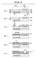
- FIG. 2 shows another example of the method of manufacturing the solid-state imaging apparatus I 1 .
- the protective film FP can be formed to cover the region R 2 and a region (for example, a region including an optical black pixel or dummy pixel or a region where a peripheral circuit or the like is provided) other than the effective pixel region. Note that the steps other than 2 C of FIG. 2 are the same as in FIG. 1 , and a description thereof will be omitted.
- FIGS. 3 and 4 A method of manufacturing a solid-state imaging apparatus I 2 according to the second embodiment will be described with reference to FIGS. 3 and 4 .
- the protective film FP is formed when forming the first color filter 106 so as to protect the electrode 103 from processes including the formation process of the second color filter 108 and the third color filter 109 .
- the protective film FP need only be formed together with one of the color filters, and may be formed together with, for example, the second color filter 108 .
- FIG. 3 schematically illustrates an example of a method of manufacturing the solid-state imaging apparatus I 2 in several steps.
- an electrode 103 is formed in a region R 2 of a structure 102 provided on a substrate 100 .
- a protective film 104 is formed on the electrode 103 and the structure 102 and covers them.
- an opening 105 is formed in a portion of the protective film 104 inside the outer edge of a convex portion P formed by the steps between the electrode 103 and the structure 102 so as to expose a portion (first portion 103 P) of the upper face of the electrode 103 .
- a first color filter 106 (green color filter) is formed immediately above one of photoelectric conversion portions 101 corresponding to, for example, a green pixel in a region R 1 .
- a second color filter 108 (blue color filter) is formed immediately above one of the photoelectric conversion portions 101 corresponding to, for example, a blue pixel in the region R 1 .
- a protective film FP is formed using the color filter material of the color filter 108 so as to cover the protective film 104 and the portion 103 P.
- the protective film FP is formed by patterning a film of the color filter material, as in the first embodiment ( 1 C of FIG. 1 ). The patterning can be performed such that a distance L 1 from the outer edge of the convex portion P to the outer edge of the protective film FP becomes, for example, 40 [ ⁇ m] or more.
- the protective film FP protects the electrode 103 from subsequent processes.
- a third color filter 109 (red color filter) is formed immediately above one of the photoelectric conversion portions 101 corresponding to, for example, a red pixel in the region R 1 .
- a planarization film 110 is formed across the regions R 1 and R 2 .
- An optical system (for example, microlenses 111 corresponding to the photoelectric conversion portions 101 ) is formed on the planarization film 110 .
- the planarization film 110 and the protective film FP are selectively removed by etching in the region R 2 , thereby forming an opening 112 to expose the upper face of the electrode 103 .
- the solid-state imaging apparatus I 2 is thus obtained.
- the protective film FP may be formed together with another color filter. According to this embodiment as well, the same effect as in the first embodiment can be obtained. More specifically, striations that may occur upon spin coating to be performed later are prevented. Hence, according to this embodiment, this is advantageous in manufacturing the solid-state imaging apparatus I 2 .
- the protective film FP is formed such that a distance L 1 from the outer edge of the convex portion P to the outer edge of the protective film FP becomes, for example, 40 [ ⁇ m] or more.
- the protective film FP may be formed to cover a region other than the region R 1 in addition to the region R 2 , as needed.
- FIG. 4 shows another example of the method of manufacturing the solid-state imaging apparatus I 2 .
- the protective film FP can be formed to cover the region R 2 and a region (for example, a region including an optical black pixel or dummy pixel or a region where a peripheral circuit or the like is provided) other than the effective pixel region. Note that the steps other than 4 D of FIG. 4 are the same as in FIG. 3 , and a description thereof will be omitted.
- the present invention is not limited to those. Changes and modifications can appropriately be made in accordance with objects, states, application purposes, functions, and other specifications, and the present invention can also be implemented by other embodiments.
- a form has been exemplified in which the protective film FP is formed together with a color filter.
- the present invention is not limited to this, and can include a case where the protective film FP is formed together with another film.
- the above-described various kinds of films can be either single-layer films or multilayer films.
- the present invention has been described by exemplifying a solid-state imaging apparatus included in an imaging system represented by a camera or the like.
- the concept of the imaging system includes not only apparatuses primarily aiming at shooting but also apparatuses (for example, personal computer and portable terminal) secondarily having a shooting function.
- the imaging system can include the solid-state imaging apparatus exemplified in the above embodiments, and a processor that processes a signal output from the solid-state imaging apparatus.
- the processor can include, for example, an A/D converter, and a processor that processes digital data output from the A/D converter.
Abstract
A method of manufacturing a semiconductor apparatus comprising forming an electrode on a structure provided on a substrate, the structure including a wiring pattern and an interlayer insulation film, forming a first film covering the electrode and the structure, forming an opening in a portion of the first film inside an outer edge of a convex portion formed by steps between upper faces of the electrode and the structure so as to expose a first portion as a portion of the upper face of the electrode, forming a second film covering the first film and the first portion, forming a protective film covering the first portion, the convex portion, and a periphery of the convex portion by patterning the second film, and forming a third film on the first film and the protective film by spin coating.
Description
1. Field of the Invention
The present invention relates to a method of manufacturing a semiconductor apparatus.
2. Description of the Related Art
In steps of manufacture of a semiconductor apparatus, spin coating is used as a method of forming (depositing) a film on a base material including a wafer. In this method, a coating liquid is supplied while rotating a wafer, thereby forming a film on the entire wafer. If the upper face of the wafer has steps, these steps may cause stripes and unevenness (so-called striations) in the film formed by spin coating. Hence, steps (difference of elevation) locally formed on the upper face of a wafer are not preferable.
A semiconductor apparatus is provided with an electrode so as to be electrically connected to an external apparatus, and a convex shape is formed on the upper face of a wafer by the electrode. This convex shape may lead to steps on the upper face of the wafer. For example, when the electrode is covered with a protective film that has an opening to partially expose the upper face of the electrode, the upper face of the protective film follows the convex shape, and steps may locally be formed on the upper face of the wafer. Hence, when further depositing a film on the semiconductor apparatus by spin coating, consideration is needed not to form the above-described striations.
The present invention provides a technique advantageous in deposition by spin coating in steps of manufacture of a semiconductor apparatus.
One of the aspects of the present invention provides a method of manufacturing a semiconductor apparatus, comprising forming an electrode on a structure, provided on a substrate, including a wiring pattern and an interlayer insulation film, forming a first film having insulating properties and covering the electrode and the structure, forming an opening in a portion of the first film inside an outer edge of a convex portion formed by steps between an upper face of the electrode and an upper face of the structure so as to expose a first portion as a portion of the upper face of the electrode, forming a second film covering the first film and the first portion, forming a protective film covering the first portion, the convex portion, and a periphery of the convex portion by patterning the second film, and forming a third film on the first film and the protective film by spin coating.
Further features of the present invention will become apparent from the following description of exemplary embodiments with reference to the attached drawings.
A manufacturing method according to the present invention will now be described by exemplifying a solid-state imaging apparatus as a semiconductor apparatus. However, the present invention is applicable to any other semiconductor apparatuses as well.
(First Embodiment)
A method of manufacturing a solid-state imaging apparatus I1 according to the first embodiment will be described with reference to FIGS. 1 and 2 . Note that the solid-state imaging apparatus I1 can be manufactured by a known semiconductor manufacturing process, and the manufacturing method to be described below is merely an embodiment of the present invention.
First, as shown in 1A of FIG. 1 , a substrate 100 including a plurality of photoelectric conversion portions 101 arrayed in the region R1 is prepared. The substrate 100 is obtained by, for example, forming elements such as transistors and photodiodes on a semiconductor substrate by semiconductor manufacturing processes including vapor deposition, patterning, and ion implantation. Alternatively, a substrate on which the elements are already formed may be prepared.
A structure 102 including a wiring pattern and an interlayer insulation film is provided on the substrate 100. The structure 102 can be formed by, for example, alternately providing insulation layers and wiring layers. An electrode 103 is formed in the region R2 of the structure 102. Note that the electrode 103 can include not only an electrode configured to read out a signal obtained by the photoelectric conversion portions 101 but also an electrode configured to supply power to a control signal to read out the signal. A protective film 104 (first film having insulating properties) is formed on the electrode 103 and the structure 102 and covers them.
As shown in 1B of FIG. 1 , an opening 105 is formed in a portion of the protective film 104 inside the outer edge of a convex portion P formed by the steps between the electrode 103 and the structure 102 so as to expose a portion (first portion 103P) of the upper face of the electrode 103. In other words, the opening 105 is formed inside the outer edge of the electrode 103 when the upper face of the substrate 100 is viewed from the upper side. The steps indicate the difference of elevation generated between the upper face of the electrode 103 and that of the structure 102. For example, in an arrangement in which the film thickness of the protective film 104 is smaller than that of the electrode 103, the convex portion P is a portion at which the upper face of the protective film 104 is located on the electrode 103. The outer edge of the convex portion P can be said to be an end of a region where the upper face of the protective film 104 is flat on the structure 102 in a direction from above the electrode 103 to its outer edge.
As shown in 1C of FIG. 1 , a first color filter 106 (green color filter) is formed immediately above one of the photoelectric conversion portions 101 corresponding to, for example, a green pixel in the region R1. The color filter 106 can be obtained by applying a color filter material and then performing patterning by exposure processing and development processing.
In the region R2, a protective film FP is formed using the color filter material so as to cover the protective film 104 and the portion 103P. The protective film FP is formed together with the color filter 106 by forming a film (second film) of the color filter material on the protective film 104 and the portion 103P by spin coating and then patterning the film. The protective film FP is formed to cover the convex portion P, the portion 103P, and their periphery, and protects the electrode 103 (portion 103P) from processing to be performed later. That is, the protective film FP is formed on the protective film 104 on the electrode 103 and on the protective film 104 that is not located on the electrode 103. The protective film FP extends from the protective film 104 on the electrode 103 to a portion out of the protective film 104 that is not located on the electrode 103 at which at least the upper face of the protective film FP flattens. The above-described patterning (patterning of the film of the color filter material) for formation of the protective film FP is performed such that a distance L1 from the outer edge of the convex portion P to the outer edge of the protective film FP becomes, for example, 40 [μm] or more. The film thickness of the film of the color filter material is preferably larger than the thickness of the electrode 103. This reduces the influence of the difference of elevation at the convex portion P in exposure processing.
As shown in 1D of FIG. 1 , a second color filter 108 (blue color filter) is formed immediately above one of the photoelectric conversion portions 101 corresponding to, for example, a blue pixel in the region R1. In a similar manner, a third color filter 109 (red color filter) is formed immediately above one of the photoelectric conversion portions 101 corresponding to a red pixel. The color filters 108 and 109 are formed by forming a film of a color filter member by spin coating and then performing exposure processing and development processing, like the above-described color filter 106.
As shown in 1E of FIG. 1 , a planarization film 110 is formed across the regions R1 and R2. An optical system including microlenses 111 corresponding to the photoelectric conversion portions 101 is formed on the planarization film 110. The microlenses 111 are formed by applying a microlens member and then performing exposure processing and development processing or by a reflow method. Note that in this embodiment, the protective film FP is formed from a color filter member, and does not use any other member (second planarization film or the like). Hence, the distance between the photoelectric conversion portions 101 and the microlenses 111 shortens, and the light sensitivity of the solid-state imaging apparatus I1 can improve.
Finally, as shown in 1F of FIG. 1 , the planarization film 110 and the protective film FP are selectively removed by etching in the region R2, thereby forming an opening 112 to expose the upper face of the electrode 103. The solid-state imaging apparatus I1 is thus obtained and then mounted on a mount substrate using wire bonding or the like.
As described above, according to this embodiment, the protective film FP is formed across the convex portion P, the portion 103P, and their periphery, as shown in 1C of FIG. 1 , thereby preventing the difference of elevation from locally becomes large. More specifically, according to this embodiment, the local difference of elevation on the upper face is small as compared to a case where the protective film FP is formed to cover, for example, only the upper face of the convex portion P and that of the portion 103P. This prevents striations that may occur upon spin coating to be performed later. In addition, the protective film FP protects the electrode 103 from subsequent processes, for example, corrosion by a developer in exposure processing and development processing. Hence, according to this embodiment, the protective film FP protects the electrode 103 while preventing occurrence of striations. This is advantageous in manufacturing the solid-state imaging apparatus I1.
In this embodiment, the protective film FP is formed such that the distance L1 from the outer edge of the convex portion P to the outer edge of the protective film FP becomes, for example, 40 [μm] or more. However, the present invention is not limited to this. The protective film FP may be formed to cover a region other than the region R1 in addition to the region R2, as needed. FIG. 2 shows another example of the method of manufacturing the solid-state imaging apparatus I1. As shown in 2C of FIG. 2 , the protective film FP can be formed to cover the region R2 and a region (for example, a region including an optical black pixel or dummy pixel or a region where a peripheral circuit or the like is provided) other than the effective pixel region. Note that the steps other than 2C of FIG. 2 are the same as in FIG. 1 , and a description thereof will be omitted.
(Second Embodiment)
A method of manufacturing a solid-state imaging apparatus I2 according to the second embodiment will be described with reference to FIGS. 3 and 4 . In the first embodiment, a form has been exemplified in which the protective film FP is formed when forming the first color filter 106 so as to protect the electrode 103 from processes including the formation process of the second color filter 108 and the third color filter 109. However, the present invention is not limited to this. The protective film FP need only be formed together with one of the color filters, and may be formed together with, for example, the second color filter 108. FIG. 3 schematically illustrates an example of a method of manufacturing the solid-state imaging apparatus I2 in several steps.
First, as shown in 3A of FIG. 3 , an electrode 103 is formed in a region R2 of a structure 102 provided on a substrate 100. A protective film 104 is formed on the electrode 103 and the structure 102 and covers them.
As shown in 3B of FIG. 3 , an opening 105 is formed in a portion of the protective film 104 inside the outer edge of a convex portion P formed by the steps between the electrode 103 and the structure 102 so as to expose a portion (first portion 103P) of the upper face of the electrode 103.
As shown in 3C of FIG. 3 , a first color filter 106 (green color filter) is formed immediately above one of photoelectric conversion portions 101 corresponding to, for example, a green pixel in a region R1.
As shown in 3D of FIG. 3 , a second color filter 108 (blue color filter) is formed immediately above one of the photoelectric conversion portions 101 corresponding to, for example, a blue pixel in the region R1. In the region R2, a protective film FP is formed using the color filter material of the color filter 108 so as to cover the protective film 104 and the portion 103P. The protective film FP is formed by patterning a film of the color filter material, as in the first embodiment (1C of FIG. 1 ). The patterning can be performed such that a distance L1 from the outer edge of the convex portion P to the outer edge of the protective film FP becomes, for example, 40 [μm] or more. The protective film FP protects the electrode 103 from subsequent processes.
As shown in 3E of FIG. 3 , a third color filter 109 (red color filter) is formed immediately above one of the photoelectric conversion portions 101 corresponding to, for example, a red pixel in the region R1.
As shown in 3F of FIG. 3 , a planarization film 110 is formed across the regions R1 and R2. An optical system (for example, microlenses 111 corresponding to the photoelectric conversion portions 101) is formed on the planarization film 110.
Finally, as shown in 3G of FIG. 3 , the planarization film 110 and the protective film FP are selectively removed by etching in the region R2, thereby forming an opening 112 to expose the upper face of the electrode 103. The solid-state imaging apparatus I2 is thus obtained.
As described above, the protective film FP may be formed together with another color filter. According to this embodiment as well, the same effect as in the first embodiment can be obtained. More specifically, striations that may occur upon spin coating to be performed later are prevented. Hence, according to this embodiment, this is advantageous in manufacturing the solid-state imaging apparatus I2.
In this embodiment, the protective film FP is formed such that a distance L1 from the outer edge of the convex portion P to the outer edge of the protective film FP becomes, for example, 40 [μm] or more. However, the present invention is not limited to this. The protective film FP may be formed to cover a region other than the region R1 in addition to the region R2, as needed. FIG. 4 shows another example of the method of manufacturing the solid-state imaging apparatus I2. As shown in 4D of FIG. 4 , the protective film FP can be formed to cover the region R2 and a region (for example, a region including an optical black pixel or dummy pixel or a region where a peripheral circuit or the like is provided) other than the effective pixel region. Note that the steps other than 4D of FIG. 4 are the same as in FIG. 3 , and a description thereof will be omitted.
Two embodiments have been described above. However, the present invention is not limited to those. Changes and modifications can appropriately be made in accordance with objects, states, application purposes, functions, and other specifications, and the present invention can also be implemented by other embodiments. For example, in the above-described embodiments, a form has been exemplified in which the protective film FP is formed together with a color filter. However, the present invention is not limited to this, and can include a case where the protective film FP is formed together with another film. Additionally, for example, the above-described various kinds of films can be either single-layer films or multilayer films.
In the above embodiments, the present invention has been described by exemplifying a solid-state imaging apparatus included in an imaging system represented by a camera or the like. The concept of the imaging system includes not only apparatuses primarily aiming at shooting but also apparatuses (for example, personal computer and portable terminal) secondarily having a shooting function. The imaging system can include the solid-state imaging apparatus exemplified in the above embodiments, and a processor that processes a signal output from the solid-state imaging apparatus. The processor can include, for example, an A/D converter, and a processor that processes digital data output from the A/D converter.
While the present invention has been described with reference to exemplary embodiments, it is to be understood that the invention is not limited to the disclosed exemplary embodiments. The scope of the following claims is to be accorded the broadest interpretation so as to encompass all such modifications and equivalent structures and functions.
This application claims the benefit of Japanese Patent Application No. 2013-172662, filed Aug. 22, 2013, which is hereby incorporated by reference herein in its entirety.
Claims (8)
1. A method of manufacturing a solid-state imaging apparatus, comprising a plurality of photoelectric conversion portions arranged on a substrate, a plurality of microlenses provided in correspondence with the plurality of photoelectric conversion portions, and a plurality of color filters provided between the plurality of photoelectric conversion portions and the plurality of microlenses,
the method comprising:
forming an electrode on a structure provided on the substrate, the structure including a wiring pattern and an interlayer insulation film;
forming a first film having insulating properties, the first film covering the electrode and the structure;
forming an opening in a portion of the first film inside an outer edge of a convex portion formed by steps between an upper face of the electrode and an upper face of the structure so as to expose a first portion as a portion of the upper face of the electrode;
forming a second film covering the first film and the first portion;
patterning the second film to form a first color filter and a protective film simultaneously, the first color filter being one of the plurality of color filters, and the protective film covering the first portion, the convex portion, and a periphery of the convex portion; and
forming a third film on the first film and the protective film by spin coating.
2. The method according to claim 1 , wherein the apparatus includes a pixel region and an electrode region when viewed from an upper side,
wherein the plurality of photoelectric conversion portions, the plurality of microlenses, and the plurality of color filters are provided in the pixel region,
wherein the electrode and the protective film are provided in the electrode region, and
wherein, in the patterning the second film, the second film is patterned such that, in the electrode region among the pixel region and the electrode region, a distance from the outer edge of the convex portion of the first film to an outer edge of the protective film becomes not less than 40 μm.
3. The method according to claim 1 , wherein the protective film is made of the same member as the first color filter having one of a plurality of colors.
4. The method according to claim 1 , further comprising forming a second color filter having a color different from the first color filter by performing exposure processing and development processing for the third film formed in the forming the third film.
5. The method according to claim 4 , further comprising forming a third color filter before the forming the third film.
6. The method according to claim 1 , further comprising, after the forming the third film, removing the protective film and the third film and forming an opening so as to partially expose the upper face of the electrode.
7. The method according to claim 1 , wherein a thickness of the second film is larger than that of the electrode.
8. The method according to claim 1 , wherein the second film covers the first film located on the electrode, and covers the first film that is not located on the electrode and has a flat upper face.
Applications Claiming Priority (2)
| Application Number | Priority Date | Filing Date | Title |
|---|---|---|---|
| JP2013-172662 | 2013-08-22 | ||
| JP2013172662A JP6168915B2 (en) | 2013-08-22 | 2013-08-22 | Manufacturing method of semiconductor device |
Publications (2)
| Publication Number | Publication Date |
|---|---|
| US20150056741A1 US20150056741A1 (en) | 2015-02-26 |
| US9412785B2 true US9412785B2 (en) | 2016-08-09 |
Family
ID=52480726
Family Applications (1)
| Application Number | Title | Priority Date | Filing Date |
|---|---|---|---|
| US14/337,488 Active 2034-12-11 US9412785B2 (en) | 2013-08-22 | 2014-07-22 | Method of manufacturing semiconductor apparatus |
Country Status (2)
| Country | Link |
|---|---|
| US (1) | US9412785B2 (en) |
| JP (1) | JP6168915B2 (en) |
Cited By (1)
| Publication number | Priority date | Publication date | Assignee | Title |
|---|---|---|---|---|
| US20160293657A1 (en) * | 2015-04-06 | 2016-10-06 | Canon Kabushiki Kaisha | Method of manufacturing solid-state image sensor, solid-state image sensor, and camera |
Families Citing this family (3)
| Publication number | Priority date | Publication date | Assignee | Title |
|---|---|---|---|---|
| JP6168915B2 (en) * | 2013-08-22 | 2017-07-26 | キヤノン株式会社 | Manufacturing method of semiconductor device |
| JP6433208B2 (en) | 2014-02-20 | 2018-12-05 | キヤノン株式会社 | Method for manufacturing solid-state imaging device |
| JP2019012739A (en) * | 2017-06-29 | 2019-01-24 | ソニーセミコンダクタソリューションズ株式会社 | Solid state imaging device and imaging apparatus |
Citations (32)
| Publication number | Priority date | Publication date | Assignee | Title |
|---|---|---|---|---|
| US20010043043A1 (en) * | 2000-01-07 | 2001-11-22 | Megumi Aoyama | Organic electroluminescent display panel and organic electroluminescent device used therefor |
| US6472698B1 (en) * | 1999-09-21 | 2002-10-29 | Nec Corporation | Solid state image sensor and method for fabricating the same |
| US20050090035A1 (en) * | 2003-10-24 | 2005-04-28 | Mangnachip Semiconductor, Ltd. | Method for fabricating CMOS image sensor protecting low temperature oxide delamination |
| US20060118795A1 (en) * | 2004-07-06 | 2006-06-08 | Fuji Photo Film Co., Ltd. | Functional device and method for producing the same |
| US20060141654A1 (en) * | 2004-12-24 | 2006-06-29 | Lim Bi O | Method for fabricating a CMOS image sensor |
| US20060138578A1 (en) * | 2004-12-29 | 2006-06-29 | Lim Keun H | CMOS image sensor and method for fabricating the same |
| US20060292734A1 (en) * | 2005-06-27 | 2006-12-28 | Dongbu Electronics Co., Ltd. | Method for manufacturing CMOS image sensor |
| JP2007073966A (en) | 2005-09-08 | 2007-03-22 | Magnachip Semiconductor Ltd | Method for manufacturing image sensor capable of saving lto (linear tape-open) protective film |
| JP2007088459A (en) | 2005-09-22 | 2007-04-05 | Samsung Electronics Co Ltd | Method for forming image sensor and image sensor formed by it |
| US20070082423A1 (en) * | 2005-09-21 | 2007-04-12 | Lee Sang G | Method of fabricating CMOS image sensor |
| US20080001155A1 (en) * | 2006-06-30 | 2008-01-03 | Lg Philips Lcd Co., Ltd. | Array substrate for liquid crystal display device and method of fabricating the same |
| JP2008034521A (en) | 2006-07-27 | 2008-02-14 | Matsushita Electric Ind Co Ltd | Solid-state imaging apparatus, and manufacturing method thereof |
| JP2008032521A (en) | 2006-07-28 | 2008-02-14 | Icom Inc | Fall detector, and method, and computer program |
| US20080150060A1 (en) * | 2006-12-20 | 2008-06-26 | Dongbu Hitek Co., Ltd. | Image sensor and method for manufacturing the same |
| US20080150058A1 (en) * | 2006-12-26 | 2008-06-26 | Jeong-Su Park | Image sensor and method for manufacturing the same |
| US20080224136A1 (en) * | 2007-03-15 | 2008-09-18 | Hsin-Heng Wang | Image sensor and fabrication method thereof |
| US20090146236A1 (en) * | 2007-12-07 | 2009-06-11 | Cheil Industries Inc. | Photosensitive resin composition for pad protective layer, and method for making image sensor using the same |
| US20090146150A1 (en) * | 2007-12-05 | 2009-06-11 | Semiconductor Energy Laboratory Co., Ltd | Display Device and Method for Manufacturing the Same |
| US20090170233A1 (en) * | 2007-12-28 | 2009-07-02 | Young-Je Yun | Method for fabricating cmos image sensor |
| US20100323458A1 (en) * | 2007-12-21 | 2010-12-23 | E2V Semiconductors | METHOD FOR MAKING P(VDF/TrFE) COPOLYMER LAYER SENSORS, AND CORRESPONDING SENSOR |
| US20110024858A1 (en) * | 2009-07-30 | 2011-02-03 | Sony Corporation | Solid-state imaging device and method for producing the same |
| US20120052606A1 (en) * | 2010-08-27 | 2012-03-01 | Semiconductor Energy Laboratory Co., Ltd. | Manufacturing methods of semiconductor device and light-emitting display device |
| US20120217498A1 (en) * | 2009-09-01 | 2012-08-30 | Rohm Co., Ltd. | Photoelectric converter and method for manufacturing the same |
| US20130334656A1 (en) * | 2012-06-13 | 2013-12-19 | Samsung Electronics Co., Ltd. | Electrical interconnection structures including stress buffer layers |
| US20130335590A1 (en) * | 2012-06-15 | 2013-12-19 | Canon Kabushiki Kaisha | Solid-state image sensor, method of manufacturing the same, and camera |
| US8753917B2 (en) * | 2010-12-14 | 2014-06-17 | International Business Machines Corporation | Method of fabricating photoconductor-on-active pixel device |
| US20140339543A1 (en) * | 2013-05-18 | 2014-11-20 | Semiconductor Energy Laboratory Co., Ltd. | Semiconductor device |
| US20150001503A1 (en) * | 2013-07-01 | 2015-01-01 | Sony Corporation | Image pickup device and electronic apparatus |
| US20150056741A1 (en) * | 2013-08-22 | 2015-02-26 | Canon Kabushiki Kaisha | Method of manufacturing semiconductor apparatus |
| US20150236069A1 (en) * | 2014-02-20 | 2015-08-20 | Canon Kabushiki Kaisha | Method of manufacturing semiconductor apparatus |
| US9129957B1 (en) * | 2014-05-07 | 2015-09-08 | Chung Yuan Christian University | Method of forming a metal bump |
| US20150303226A1 (en) * | 2014-04-18 | 2015-10-22 | Canon Kabushiki Kaisha | Photoelectric conversion element and method of manufacturing the same |
Family Cites Families (2)
| Publication number | Priority date | Publication date | Assignee | Title |
|---|---|---|---|---|
| JPH0214569A (en) * | 1988-07-01 | 1990-01-18 | Minolta Camera Co Ltd | Manufacture of color sensor |
| KR100504563B1 (en) * | 2004-08-24 | 2005-08-01 | 동부아남반도체 주식회사 | Method for fabricating an image sensor |
-
2013
- 2013-08-22 JP JP2013172662A patent/JP6168915B2/en active Active
-
2014
- 2014-07-22 US US14/337,488 patent/US9412785B2/en active Active
Patent Citations (34)
| Publication number | Priority date | Publication date | Assignee | Title |
|---|---|---|---|---|
| US6472698B1 (en) * | 1999-09-21 | 2002-10-29 | Nec Corporation | Solid state image sensor and method for fabricating the same |
| US20010043043A1 (en) * | 2000-01-07 | 2001-11-22 | Megumi Aoyama | Organic electroluminescent display panel and organic electroluminescent device used therefor |
| US20050090035A1 (en) * | 2003-10-24 | 2005-04-28 | Mangnachip Semiconductor, Ltd. | Method for fabricating CMOS image sensor protecting low temperature oxide delamination |
| US20060118795A1 (en) * | 2004-07-06 | 2006-06-08 | Fuji Photo Film Co., Ltd. | Functional device and method for producing the same |
| US20060141654A1 (en) * | 2004-12-24 | 2006-06-29 | Lim Bi O | Method for fabricating a CMOS image sensor |
| US20060138578A1 (en) * | 2004-12-29 | 2006-06-29 | Lim Keun H | CMOS image sensor and method for fabricating the same |
| US20060292734A1 (en) * | 2005-06-27 | 2006-12-28 | Dongbu Electronics Co., Ltd. | Method for manufacturing CMOS image sensor |
| US7294524B2 (en) | 2005-09-08 | 2007-11-13 | Magnachip Semiconductor, Ltd. | Method for fabricating image sensor without LTO-based passivation layer |
| JP2007073966A (en) | 2005-09-08 | 2007-03-22 | Magnachip Semiconductor Ltd | Method for manufacturing image sensor capable of saving lto (linear tape-open) protective film |
| US20070082423A1 (en) * | 2005-09-21 | 2007-04-12 | Lee Sang G | Method of fabricating CMOS image sensor |
| JP2007088459A (en) | 2005-09-22 | 2007-04-05 | Samsung Electronics Co Ltd | Method for forming image sensor and image sensor formed by it |
| US7919350B2 (en) | 2005-09-22 | 2011-04-05 | Samsung Electronics Co., Ltd. | Image sensor and method of making same |
| US20080001155A1 (en) * | 2006-06-30 | 2008-01-03 | Lg Philips Lcd Co., Ltd. | Array substrate for liquid crystal display device and method of fabricating the same |
| JP2008034521A (en) | 2006-07-27 | 2008-02-14 | Matsushita Electric Ind Co Ltd | Solid-state imaging apparatus, and manufacturing method thereof |
| JP2008032521A (en) | 2006-07-28 | 2008-02-14 | Icom Inc | Fall detector, and method, and computer program |
| US20080150060A1 (en) * | 2006-12-20 | 2008-06-26 | Dongbu Hitek Co., Ltd. | Image sensor and method for manufacturing the same |
| US20080150058A1 (en) * | 2006-12-26 | 2008-06-26 | Jeong-Su Park | Image sensor and method for manufacturing the same |
| US20080224136A1 (en) * | 2007-03-15 | 2008-09-18 | Hsin-Heng Wang | Image sensor and fabrication method thereof |
| US20090146150A1 (en) * | 2007-12-05 | 2009-06-11 | Semiconductor Energy Laboratory Co., Ltd | Display Device and Method for Manufacturing the Same |
| US20090146236A1 (en) * | 2007-12-07 | 2009-06-11 | Cheil Industries Inc. | Photosensitive resin composition for pad protective layer, and method for making image sensor using the same |
| US20100323458A1 (en) * | 2007-12-21 | 2010-12-23 | E2V Semiconductors | METHOD FOR MAKING P(VDF/TrFE) COPOLYMER LAYER SENSORS, AND CORRESPONDING SENSOR |
| US20090170233A1 (en) * | 2007-12-28 | 2009-07-02 | Young-Je Yun | Method for fabricating cmos image sensor |
| US20110024858A1 (en) * | 2009-07-30 | 2011-02-03 | Sony Corporation | Solid-state imaging device and method for producing the same |
| US20120217498A1 (en) * | 2009-09-01 | 2012-08-30 | Rohm Co., Ltd. | Photoelectric converter and method for manufacturing the same |
| US20120052606A1 (en) * | 2010-08-27 | 2012-03-01 | Semiconductor Energy Laboratory Co., Ltd. | Manufacturing methods of semiconductor device and light-emitting display device |
| US8753917B2 (en) * | 2010-12-14 | 2014-06-17 | International Business Machines Corporation | Method of fabricating photoconductor-on-active pixel device |
| US20130334656A1 (en) * | 2012-06-13 | 2013-12-19 | Samsung Electronics Co., Ltd. | Electrical interconnection structures including stress buffer layers |
| US20130335590A1 (en) * | 2012-06-15 | 2013-12-19 | Canon Kabushiki Kaisha | Solid-state image sensor, method of manufacturing the same, and camera |
| US20140339543A1 (en) * | 2013-05-18 | 2014-11-20 | Semiconductor Energy Laboratory Co., Ltd. | Semiconductor device |
| US20150001503A1 (en) * | 2013-07-01 | 2015-01-01 | Sony Corporation | Image pickup device and electronic apparatus |
| US20150056741A1 (en) * | 2013-08-22 | 2015-02-26 | Canon Kabushiki Kaisha | Method of manufacturing semiconductor apparatus |
| US20150236069A1 (en) * | 2014-02-20 | 2015-08-20 | Canon Kabushiki Kaisha | Method of manufacturing semiconductor apparatus |
| US20150303226A1 (en) * | 2014-04-18 | 2015-10-22 | Canon Kabushiki Kaisha | Photoelectric conversion element and method of manufacturing the same |
| US9129957B1 (en) * | 2014-05-07 | 2015-09-08 | Chung Yuan Christian University | Method of forming a metal bump |
Cited By (2)
| Publication number | Priority date | Publication date | Assignee | Title |
|---|---|---|---|---|
| US20160293657A1 (en) * | 2015-04-06 | 2016-10-06 | Canon Kabushiki Kaisha | Method of manufacturing solid-state image sensor, solid-state image sensor, and camera |
| US9893110B2 (en) * | 2015-04-06 | 2018-02-13 | Canon Kabushiki Kaisha | Method of manufacturing solid-state image sensor, solid-state image sensor, and camera |
Also Published As
| Publication number | Publication date |
|---|---|
| US20150056741A1 (en) | 2015-02-26 |
| JP2015041711A (en) | 2015-03-02 |
| JP6168915B2 (en) | 2017-07-26 |
Similar Documents
| Publication | Publication Date | Title |
|---|---|---|
| US7498190B2 (en) | Method for fabricating a CMOS image sensor | |
| US9324755B2 (en) | Image sensors with reduced stack height | |
| US20170148841A1 (en) | Solid-state image sensor and electronic device | |
| US9412785B2 (en) | Method of manufacturing semiconductor apparatus | |
| US10468445B2 (en) | Image sensor and method for fabricating the same | |
| CN109166871B (en) | Image sensor and manufacturing method thereof | |
| US7777795B2 (en) | Solid-state image pickup device | |
| US20130001728A1 (en) | Backside illuminated image sensors with vertical light shields | |
| JP2018207086A (en) | Solid-state imaging element including microlens layer with dummy structure | |
| US9305965B2 (en) | Solid-state imaging apparatus and method of manufacturing the same | |
| US9893110B2 (en) | Method of manufacturing solid-state image sensor, solid-state image sensor, and camera | |
| US20050082627A1 (en) | CMOS image sensor and manufacturing method thereof | |
| US20080157087A1 (en) | Image sensor and method for manufacturing the same | |
| US9466640B2 (en) | Method of manufacturing semiconductor apparatus | |
| TWI550842B (en) | Image sensor | |
| KR20150017902A (en) | Image sensor having lens type color filter and method for fabricating the same | |
| JP2006216904A (en) | Color solid state image sensor and method of fabricating the same | |
| US20160021284A1 (en) | Photoelectric conversion apparatus, and imaging system using the same | |
| US10586825B2 (en) | Self-alignment of a pad and ground in an image sensor | |
| US9853083B2 (en) | Method for fabricating an image-sensor structure | |
| US9911780B1 (en) | Backside metal grid and metal pad simplification | |
| JP2012204686A (en) | Solid state image pickup device and manufacturing method of the same | |
| US20090108309A1 (en) | Cmos image sensor and method for manufacturing the same | |
| JP5510053B2 (en) | Manufacturing method of color filter for linear sensor | |
| JP2011165791A (en) | Solid-state imaging element, and method of manufacturing the same |
Legal Events
| Date | Code | Title | Description |
|---|---|---|---|
| AS | Assignment |
Owner name: CANON KABUSHIKI KAISHA, JAPAN Free format text: ASSIGNMENT OF ASSIGNORS INTEREST;ASSIGNOR:KURIHARA, MASAKI;REEL/FRAME:034522/0615 Effective date: 20140717 |
|
| STCF | Information on status: patent grant |
Free format text: PATENTED CASE |
|
| MAFP | Maintenance fee payment |
Free format text: PAYMENT OF MAINTENANCE FEE, 4TH YEAR, LARGE ENTITY (ORIGINAL EVENT CODE: M1551); ENTITY STATUS OF PATENT OWNER: LARGE ENTITY Year of fee payment: 4 |