US9411237B2 - Resist hardening and development processes for semiconductor device manufacturing - Google Patents

Resist hardening and development processes for semiconductor device manufacturing Download PDF

Info

Publication number
US9411237B2
US9411237B2 US14/205,324 US201414205324A US9411237B2 US 9411237 B2 US9411237 B2 US 9411237B2 US 201414205324 A US201414205324 A US 201414205324A US 9411237 B2 US9411237 B2 US 9411237B2
Authority
US
United States
Prior art keywords
resist layer
substrate
regions
resist
etch
Prior art date
Legal status (The legal status is an assumption and is not a legal conclusion. Google has not performed a legal analysis and makes no representation as to the accuracy of the status listed.)
Active, expires
Application number
US14/205,324
Other versions
US20140263172A1 (en
Inventor
Peng Xie
Christopher Dennis Bencher
Huixiong Dai
Timothy Michaelson
Subhash Deshmukh
Current Assignee (The listed assignees may be inaccurate. Google has not performed a legal analysis and makes no representation or warranty as to the accuracy of the list.)
Applied Materials Inc
Original Assignee
Applied Materials Inc
Priority date (The priority date is an assumption and is not a legal conclusion. Google has not performed a legal analysis and makes no representation as to the accuracy of the date listed.)
Filing date
Publication date
Application filed by Applied Materials Inc filed Critical Applied Materials Inc
Priority to US14/205,324 priority Critical patent/US9411237B2/en
Assigned to APPLIED MATERIALS, INC. reassignment APPLIED MATERIALS, INC. ASSIGNMENT OF ASSIGNORS INTEREST (SEE DOCUMENT FOR DETAILS). Assignors: DAI, HUIXIONG, DESHMUKH, SUBHASH, BENCHER, CHRISTOPHER DENNIS, MICHAELSON, TIMOTHY, XIE, PENG
Publication of US20140263172A1 publication Critical patent/US20140263172A1/en
Priority to US15/216,521 priority patent/US20160329222A1/en
Application granted granted Critical
Publication of US9411237B2 publication Critical patent/US9411237B2/en
Active legal-status Critical Current
Adjusted expiration legal-status Critical

Links

Images

Classifications

    • HELECTRICITY
    • H01ELECTRIC ELEMENTS
    • H01LSEMICONDUCTOR DEVICES NOT COVERED BY CLASS H10
    • H01L21/00Processes or apparatus adapted for the manufacture or treatment of semiconductor or solid state devices or of parts thereof
    • H01L21/67Apparatus specially adapted for handling semiconductor or electric solid state devices during manufacture or treatment thereof; Apparatus specially adapted for handling wafers during manufacture or treatment of semiconductor or electric solid state devices or components ; Apparatus not specifically provided for elsewhere
    • H01L21/67005Apparatus not specifically provided for elsewhere
    • H01L21/67011Apparatus for manufacture or treatment
    • H01L21/67017Apparatus for fluid treatment
    • H01L21/67063Apparatus for fluid treatment for etching
    • H01L21/67069Apparatus for fluid treatment for etching for drying etching
    • CCHEMISTRY; METALLURGY
    • C23COATING METALLIC MATERIAL; COATING MATERIAL WITH METALLIC MATERIAL; CHEMICAL SURFACE TREATMENT; DIFFUSION TREATMENT OF METALLIC MATERIAL; COATING BY VACUUM EVAPORATION, BY SPUTTERING, BY ION IMPLANTATION OR BY CHEMICAL VAPOUR DEPOSITION, IN GENERAL; INHIBITING CORROSION OF METALLIC MATERIAL OR INCRUSTATION IN GENERAL
    • C23CCOATING METALLIC MATERIAL; COATING MATERIAL WITH METALLIC MATERIAL; SURFACE TREATMENT OF METALLIC MATERIAL BY DIFFUSION INTO THE SURFACE, BY CHEMICAL CONVERSION OR SUBSTITUTION; COATING BY VACUUM EVAPORATION, BY SPUTTERING, BY ION IMPLANTATION OR BY CHEMICAL VAPOUR DEPOSITION, IN GENERAL
    • C23C16/00Chemical coating by decomposition of gaseous compounds, without leaving reaction products of surface material in the coating, i.e. chemical vapour deposition [CVD] processes
    • C23C16/44Chemical coating by decomposition of gaseous compounds, without leaving reaction products of surface material in the coating, i.e. chemical vapour deposition [CVD] processes characterised by the method of coating
    • C23C16/455Chemical coating by decomposition of gaseous compounds, without leaving reaction products of surface material in the coating, i.e. chemical vapour deposition [CVD] processes characterised by the method of coating characterised by the method used for introducing gases into reaction chamber or for modifying gas flows in reaction chamber
    • C23C16/45523Pulsed gas flow or change of composition over time
    • C23C16/45525Atomic layer deposition [ALD]
    • C23C16/45544Atomic layer deposition [ALD] characterized by the apparatus
    • GPHYSICS
    • G03PHOTOGRAPHY; CINEMATOGRAPHY; ANALOGOUS TECHNIQUES USING WAVES OTHER THAN OPTICAL WAVES; ELECTROGRAPHY; HOLOGRAPHY
    • G03FPHOTOMECHANICAL PRODUCTION OF TEXTURED OR PATTERNED SURFACES, e.g. FOR PRINTING, FOR PROCESSING OF SEMICONDUCTOR DEVICES; MATERIALS THEREFOR; ORIGINALS THEREFOR; APPARATUS SPECIALLY ADAPTED THEREFOR
    • G03F7/00Photomechanical, e.g. photolithographic, production of textured or patterned surfaces, e.g. printing surfaces; Materials therefor, e.g. comprising photoresists; Apparatus specially adapted therefor
    • G03F7/26Processing photosensitive materials; Apparatus therefor
    • G03F7/36Imagewise removal not covered by groups G03F7/30 - G03F7/34, e.g. using gas streams, using plasma
    • GPHYSICS
    • G03PHOTOGRAPHY; CINEMATOGRAPHY; ANALOGOUS TECHNIQUES USING WAVES OTHER THAN OPTICAL WAVES; ELECTROGRAPHY; HOLOGRAPHY
    • G03FPHOTOMECHANICAL PRODUCTION OF TEXTURED OR PATTERNED SURFACES, e.g. FOR PRINTING, FOR PROCESSING OF SEMICONDUCTOR DEVICES; MATERIALS THEREFOR; ORIGINALS THEREFOR; APPARATUS SPECIALLY ADAPTED THEREFOR
    • G03F7/00Photomechanical, e.g. photolithographic, production of textured or patterned surfaces, e.g. printing surfaces; Materials therefor, e.g. comprising photoresists; Apparatus specially adapted therefor
    • G03F7/26Processing photosensitive materials; Apparatus therefor
    • G03F7/40Treatment after imagewise removal, e.g. baking
    • G03F7/405Treatment with inorganic or organometallic reagents after imagewise removal
    • HELECTRICITY
    • H01ELECTRIC ELEMENTS
    • H01LSEMICONDUCTOR DEVICES NOT COVERED BY CLASS H10
    • H01L21/00Processes or apparatus adapted for the manufacture or treatment of semiconductor or solid state devices or of parts thereof
    • H01L21/67Apparatus specially adapted for handling semiconductor or electric solid state devices during manufacture or treatment thereof; Apparatus specially adapted for handling wafers during manufacture or treatment of semiconductor or electric solid state devices or components ; Apparatus not specifically provided for elsewhere
    • H01L21/67005Apparatus not specifically provided for elsewhere
    • H01L21/67011Apparatus for manufacture or treatment
    • H01L21/67155Apparatus for manufacturing or treating in a plurality of work-stations
    • H01L21/67161Apparatus for manufacturing or treating in a plurality of work-stations characterized by the layout of the process chambers
    • H01L21/67167Apparatus for manufacturing or treating in a plurality of work-stations characterized by the layout of the process chambers surrounding a central transfer chamber
    • HELECTRICITY
    • H01ELECTRIC ELEMENTS
    • H01LSEMICONDUCTOR DEVICES NOT COVERED BY CLASS H10
    • H01L21/00Processes or apparatus adapted for the manufacture or treatment of semiconductor or solid state devices or of parts thereof
    • H01L21/67Apparatus specially adapted for handling semiconductor or electric solid state devices during manufacture or treatment thereof; Apparatus specially adapted for handling wafers during manufacture or treatment of semiconductor or electric solid state devices or components ; Apparatus not specifically provided for elsewhere
    • H01L21/67005Apparatus not specifically provided for elsewhere
    • H01L21/67011Apparatus for manufacture or treatment
    • H01L21/67155Apparatus for manufacturing or treating in a plurality of work-stations
    • H01L21/67201Apparatus for manufacturing or treating in a plurality of work-stations characterized by the construction of the load-lock chamber
    • HELECTRICITY
    • H01ELECTRIC ELEMENTS
    • H01LSEMICONDUCTOR DEVICES NOT COVERED BY CLASS H10
    • H01L21/00Processes or apparatus adapted for the manufacture or treatment of semiconductor or solid state devices or of parts thereof
    • H01L21/67Apparatus specially adapted for handling semiconductor or electric solid state devices during manufacture or treatment thereof; Apparatus specially adapted for handling wafers during manufacture or treatment of semiconductor or electric solid state devices or components ; Apparatus not specifically provided for elsewhere
    • H01L21/683Apparatus specially adapted for handling semiconductor or electric solid state devices during manufacture or treatment thereof; Apparatus specially adapted for handling wafers during manufacture or treatment of semiconductor or electric solid state devices or components ; Apparatus not specifically provided for elsewhere for supporting or gripping
    • H01L21/687Apparatus specially adapted for handling semiconductor or electric solid state devices during manufacture or treatment thereof; Apparatus specially adapted for handling wafers during manufacture or treatment of semiconductor or electric solid state devices or components ; Apparatus not specifically provided for elsewhere for supporting or gripping using mechanical means, e.g. chucks, clamps or pinches
    • H01L21/68707Apparatus specially adapted for handling semiconductor or electric solid state devices during manufacture or treatment thereof; Apparatus specially adapted for handling wafers during manufacture or treatment of semiconductor or electric solid state devices or components ; Apparatus not specifically provided for elsewhere for supporting or gripping using mechanical means, e.g. chucks, clamps or pinches the wafers being placed on a robot blade, or gripped by a gripper for conveyance

Landscapes

  • Engineering & Computer Science (AREA)
  • General Physics & Mathematics (AREA)
  • Physics & Mathematics (AREA)
  • Chemical & Material Sciences (AREA)
  • Condensed Matter Physics & Semiconductors (AREA)
  • Manufacturing & Machinery (AREA)
  • Computer Hardware Design (AREA)
  • Microelectronics & Electronic Packaging (AREA)
  • Power Engineering (AREA)
  • Organic Chemistry (AREA)
  • Inorganic Chemistry (AREA)
  • Chemical Kinetics & Catalysis (AREA)
  • Mechanical Engineering (AREA)
  • Metallurgy (AREA)
  • Materials Engineering (AREA)
  • Robotics (AREA)
  • General Chemical & Material Sciences (AREA)
  • Photosensitive Polymer And Photoresist Processing (AREA)
  • Drying Of Semiconductors (AREA)
  • Exposure Of Semiconductors, Excluding Electron Or Ion Beam Exposure (AREA)

Abstract

In some embodiments, a method of forming an etch mask on a substrate is provided that includes (1) forming a resist layer on a substrate; (2) exposing one or more regions of the resist layer to an energy source so as to alter at least one of a physical property and a chemical property of the exposed regions; (3) performing a hardening process on the resist layer to increase the etch resistance of first regions of the resist layer relative to second regions of the resist layer, the hardening process including exposing the resist layer to one or more reactive species within an atomic layer deposition (ALD) chamber; and (4) dry etching the resist layer to remove the one or more second regions and to form a pattern in the resist layer. Other embodiments are provided.

Description

RELATED APPLICATIONS
The present application claims priority to U.S. Provisional Application 61/786,056 filed Mar. 14, 2013, and entitled “RESIST HARDENING AND DEVELOPMENT PROCESSES FOR SEMICONDUCTOR DEVICE MANUFACTURING”, which is hereby incorporated by reference herein for all purposes.
FIELD
The present invention generally relates to semiconductor device manufacturing, and more particularly is directed to patterning process (lithography) methods and apparatus.
BACKGROUND
Lithography technology has been one of the key enablers and drivers for the semiconductor industry for the past several decades. Lithography improvements have kept the cost for printing a silicon wafer roughly constant while exponentially reducing the transistor size, therefore dramatically increasing the number of transistors that can be printed per chip at a rate known as Moore's law. Integrated circuits (ICs) have been printed optically with improvements in lens and imaging material technology along with decreases in wavelength used, fueling the steady improvement of lithography technology. However, the end of optical lithography technology has been predicted by many and for many years.
Many technologies have been proposed and developed to improve on the performance of optical lithography. Some succeeded; but the cost and complexity grew rapidly. This has been true largely because it has been more economical to advance incremental improvements in the existing optical technology rather than displace it with a new one. What are needed are methods and apparatus for improving the performance of lithography without making the process non-economical or impracticable for production.
SUMMARY
In some embodiments, a method of forming an etch mask on a substrate is provided that includes (1) forming a resist layer on a substrate; (2) exposing one or more regions of the resist layer to an energy source so as to alter at least one of a physical property and a chemical property of the exposed regions; (3) performing a hardening process on the resist layer to increase the etch resistance of first regions of the resist layer relative to second regions of the resist layer, the hardening process including exposing the resist layer to one or more reactive species within an atomic layer deposition (ALD) chamber; and (4) dry etching the resist layer to remove the one or more second regions and to form a pattern in the resist layer.
In some embodiments, a method of patterning a substrate is provided that includes (1) forming a resist layer on a substrate; (2) exposing one or more regions of the resist layer to an energy source so as to alter at least one of a physical property and a chemical property of the exposed regions; (3) developing the resist layer to pattern the resist layer; (4) performing a hardening process on the patterned resist layer to increase the etch resistance of the patterned resist layer, the hardening process including exposing the patterned resist layer to one or more reactive species within an atomic layer deposition (ALD) chamber; and (5) at least one of irradiating the substrate with ultraviolet light and vibrating the substrate during at least a portion of the hardening process.
In some embodiments, a processing system configured to process a substrate is provided that includes (1) a transfer chamber having (a) a plurality of sides each configured to couple to at least one processing chamber; and (b) a substrate handler configured to transport substrates between processing chambers coupled to the transfer chamber; (2) an atomic layer deposition chamber (ALD) coupled to the transfer chamber; (3) an etch chamber coupled to the transfer chamber; and (4) a controller coupled to the transfer chamber and configured to control operation of the processing system to (a) transfer a substrate into the ALD chamber, the substrate having a patterned resist layer formed on the substrate; (b) perform a hardening process on the patterned resist layer in the ALD chamber to increase the etch resistance of the patterned resist layer, the hardening process including exposing the patterned resist layer to one or more reactive species within the ALD chamber and at least one of irradiating the substrate with ultraviolet light and vibrating the substrate during at least a portion of exposing the patterned resist layer to one or more reactive species within the ALD chamber; (c) transfer the substrate to the etch chamber; and (d) etch the substrate within the etch chamber to pattern the substrate.
In some embodiments, a processing system configured to process a substrate is provided that includes (1) an atomic layer deposition chamber (ALD) configured to perform a hardening process on a substrate having a resist layer formed on the substrate with one or more exposed regions of the resist layer at least one of physically and chemically altered by exposure to at least one of ultra-violet light, extreme-ultra-violet light and an electron beam, the hardening process increasing the etch resistance of first regions of the resist layer relative to second regions of the resist layer; (2) an etch chamber configured to receive the substrate from the ALD chamber and to etch the resist layer to remove the one or more second regions and to form a pattern in the resist layer; and (3) a controller configured to control operation of the processing system to (a) transfer the substrate into the ALD chamber; (b) perform the hardening process on the resist layer in the ALD chamber by exposing the resist layer to one or more reactive species within the ALD chamber; (c) transfer the substrate to the etch chamber; and (d) etch the resist layer within the etch chamber to remove the one or more second regions of the resist layer.
In some embodiments, a method of patterning a substrate is provided that includes (1) forming a resist layer on a substrate, the resist layer formed from two or more polymer materials using a self-assembly process; (2) performing a hardening process on the resist layer to increase the etch resistance of first polymer regions of the resist layer relative to second polymer regions of the resist layer, the hardening process including exposing the resist layer to one or more reactive species within an atomic layer deposition (ALD) chamber; (3) at least one of irradiating the substrate with ultraviolet light and vibrating the substrate during at least a portion of the hardening process; and (4) dry etching the resist layer to remove the one or more second polymer regions and to form a pattern in the resist layer.
Numerous other aspects are provided. Other features and aspects of the present invention will become more fully apparent from the following detailed description, the appended claims and the accompanying drawings.
BRIEF DESCRIPTION OF THE DRAWINGS
FIG. 1 illustrates a flowchart of a first method of transferring a pattern into a substrate provided in accordance with embodiments of the present invention.
FIGS. 2A-2F illustrate schematic cross-sectional views of a substrate processed using the method of FIG. 1 in accordance with embodiments of the present invention.
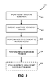
FIG. 3 illustrates a flowchart of a second method of transferring a pattern into a substrate provided in accordance with embodiments of the present invention.
FIG. 4A is an example processing system for carrying out the method of FIG. 1.
FIG. 4B is an example processing system for carrying out the method of FIG. 3.
FIG. 5 is a schematic top view of another example processing system configured to process a substrate in accordance with embodiments of the present invention.
DETAILED DESCRIPTION
Current lithography employed for semiconductor device manufacturing employs primarily four steps. These steps include (1) photoresist or “resist” coating; (2) exposure; (3) wet development; and (4) etch.
During resist coating, a substrate is coated with a layer of resist, typically using a spin-on process in which resist material is deposited on a top surface of a spinning substrate. Rotation of the substrate causes the resist material to uniformly spread across the top surface of the substrate. In conventional resists, the solubility of the resist material is changed by exposure to light or other energy through a mask pattern so that the mask pattern emerges in the resist layer upon wet development (e.g., much like a photograph). For instance, a chemically amplified resist (CAR) may include a photo-acid generator (PAG) which undergoes a photo-chemical reaction upon exposure to an energy source such as 193 nanometer light, an electron beam (e-beam), extreme ultraviolet (EUV) light, or the like. The photo-chemical reaction may produce an acid within exposed regions of the resist which alters polymer groups within the resist to create a dissolution rate contrast in the resist when the resist is exposed to a wet developer. Other mechanisms may be employed to create dissolution rate contrasts in resist materials. For example, in some resists, exposure to an appropriate energy source may render the resist less likely to dissolve in a wet developer.
During exposure, the substrate is illuminated with light or another energy source through a mask to selectively expose regions of the resist to the energy source. The exposed regions of the resist are chemically altered as described above.
During wet development, the exposed resist layer is placed in a wet chemical bath (e.g., developer) to selectively remove the resist material. For positive resist, the material exposed to light is removed by the developer; while for negative resist, the material not exposed to light is removed by the developer. This process transfers the pattern of the mask into the resist layer.
Following development, the resist layer is employed as an etch mask to transfer the pattern formed in the resist layer into the substrate (either directly or through use of one or more hard masks).
Conventional lithography processes as described above may suffer from several drawbacks. For instance, wet development of resists may produce a pattern having resist line-edge-roughness (LER) due to an acid gradient at mask edges. This may cause uncertainty in predicting line edges that result following wet development. Additionally, as device dimensions shrink below 22 nanometers, capillary forces due to the small feature size may cause pattern collapsing during wet development and cleaning processes. Wet developed resist materials also may have poor etch resistivity such that multiple hardmasks may be employed during device fabrication. This is particularly true during formation of deep trenches such as through-silicon via (TSV) etch steps, or when a thin EUV resist is employed.
Embodiments of the present invention provide methods of performing lithography using a dry development process with a hardened resist layer. For example, the dry development process may be a dry etch process, such as a reactive ion etch process. In some embodiments, a resist layer is selectively hardened, and a mask pattern is transferred to the resist layer employing a plasma etch process.
Use of such a dry development process may overcome many of the above-mentioned shortcomings. For example, employing a dry development process in place of a wet development process may improve LER and reduce pattern collapse. In other embodiments, a wet development process may be employed during formation of a hardened resist layer.
Use of a hardened resist layer may reduce the number of processing steps employed by reducing the use of some hard mask layers, and in some embodiments, allowing both the hardened resist layer and an underlying layer to be etched in a single etch chamber. Such hardened resist layers also may have sufficient etch resistivity to enable deep trench etching without additional hard mask layers. These and other embodiments are described below with reference to FIGS. 1-5.
FIG. 1 illustrates a flowchart of a first method 100 of transferring a pattern into a substrate provided in accordance with embodiments of the present invention. Method 100 is explained with reference to FIGS. 2A-2F which illustrate schematic cross-sectional views of a substrate processed using method 100.
With reference to FIG. 1 and FIG. 2A, a substrate 200 (FIG. 2A) is provided that includes a material layer 202 to be etched. The substrate 200 may be any suitable substrate such as a silicon or other semiconductor wafer, a glass plate or the like. The material layer 202 may be a portion of the substrate 200, or a separate layer such as a conductive layer, an insulating layer, another semiconductor layer, etc., and may be of any suitable thickness. The substrate 200, material layer 202 and other layers described herein are not drawn to scale.
In Block 101 (FIG. 1), a resist layer 204 is formed on the substrate 200 as shown in FIG. 2B. The resist layer 204 is a material layer that undergoes a chemical and/or physical property change when exposed to an energy source such as ultra-violet (UV) light, extreme-ultra-violet (EUV) light or an electron beam. For example, when a region of the resist layer 204 is exposed to one of the above energy sources, chemical bonds within the exposed region may be formed or broken, film density may change and/or the like. As a non-limiting example, the resist layer 204 may be a poly(methylmethacrylate) (PMMA) resist which includes C═O, C═N or other groups which may be disrupted by exposure to UV, EUV or e-beam energy. Other resists such as polystyrene-b-poly(methyl methacrylate) (PS-b-PMMA), polyhydroxystyren acrylic polymers, etc., may be employed and/or other properties such as polarity, density, bonding structure, etc., may be modified by a suitable exposure process.
In some embodiments, the resist layer 204 may be a PMMA-based resist layer having a thickness of about 150 to about 30,000 angstroms. Thinner or thicker resist layers may be employed. Because of the hardening process employed (as described below), a relatively thin layer of resist may be employed and still provide sufficient etch resistance.
A post-coating resist bake may be employed in some embodiments. For example, solvents may be present in the resist to facilitate uniform spreading of the resist layer across the substrate 200. As such, baking the substrate 200 following resist coating may drive off the solvents and “cure” the resist prior to exposure. As an example, the substrate 200 may be baked at a temperature of about 100° C. for about 1 minute in ambient air environment. Any suitable post-coating/pre-exposure bake temperature and/or environment may be employed.
In Block 102 the resist layer 204 is exposed to an energy source such as UV light, EUV light or an e-beam. With reference to FIG. 2C, a mask 206 may be placed proximate the resist layer 204. For example, the mask 206 may be placed in contact with or a short distance from the resist layer 204. The mask 206 includes transparent and opaque regions which selectively allow light energy (or another energy type) to pass through the mask 206 and expose one or more regions of the resist layer 204 (as indicated by the shaded regions 208 a-d in resist layer 204). In one example embodiment, the resist layer 204 may be exposed to light having a wavelength of about 13.5 nanometers (EUV) or about 193 or 248 nanometers (UV) at a dose on the order of about 1-30 mJ/cm2. Other wavelengths and/or doses may be employed.
As described, exposed regions of the resist layer 204 undergo a chemical and/or physical change. For example, when a PMMA resist is employed for resist layer 204, exposed regions of the resist layer 204 may have a smaller density of C═O, C═N or other groups following exposure. As will be described below, in some embodiments, subsequent processing of the resist layer 204 may increase the etch resistance of non-exposed regions 210 a-e (FIG. 2D) of the resist layer 204 relative to exposed regions 208 a-d of the resist layer 204. In other embodiments, subsequent processing of the resist layer 204 may increase the etch resistance of exposed regions 208 a-d of the resist layer 204 relative to non-exposed regions 210 a-e of the resist layer 204.
In Block 103 a hardening process is performed on the exposed resist layer 204. In some embodiments, the substrate 200 is loaded into an atomic layer deposition (ALD) chamber and exposed to one or more reactive species to selectively harden the resist layer 204. For example, the resist layer 204 may be exposed to a metal precursor within the ALD chamber to increase the etch resistance of non-exposed regions 210 a-e of the resist layer 204 relative to exposed regions 208 a-d of the resist layer 204 (or vice versa). Example metal precursors include sources of aluminum, titanium, zinc, tungsten, silicon, hafnium, zirconium and/or other metals and/or similar materials.
In one example embodiment, trimethylaluminum (TMA) and water may be deposited on the resist layer 204 using either a sequential or simultaneous deposition/etch ALD process. For example, in a sequential process, TMA may be employed to expose the resist layer 204 to aluminum, and to incorporate aluminum in the resist layer 204. Water or another oxygen source may then be employed to oxidize the aluminum and form aluminum oxide (Al2O3) within the resist layer 204. In some embodiments, TMA may be supplied for less than about 1 second to about 600 seconds at a pressure of about 1 to about 50 Torr and at a substrate temperature of about 60 to about 150° C. Water may be supplied for less than about 1 second to about 600 seconds at a pressure of about 1 to about 50 Torr and at a substrate temperature of about 60 to about 150° C. Other metal precursors and/or process conditions may be employed.
In some embodiments, use of a metal source such as TMA and water for hardening the resist layer 204 may be time consuming, as multiple cycles of TMA and water purge are employed to fully and/or adequately harden the resist layer 204. In such embodiments, the mechanism for absorption, diffusion and desorption reactions during the exposure-purge-exposure-purge cycle may be complicated. To improve throughput, a furnace-based or other batch process may be employed.
In other embodiments, irradiation may be employed to assist the resist hardening process. For example, during metal source (e.g., TMA) exposure, additional irradiation may be introduced to facilitate more bonding reactions (e.g., through absorption and/or photochemical reaction). The bonding energy of the resist polymer chain may change upon irradiation and create new TMA bonding/nucleation sites. In addition, irradiation may also generate new C═O or other bonds, or in some embodiments, reduce the number of C═O or other bonds.
Irradiation during the resist hardening process may serve as a catalyst for, or otherwise facilitate, reactions between a precursor and the resist. In some embodiments, this may allow resist hardening without or with a reduced amount of a second reactant such as water and/or reduce out-diffusion during pumping between precursor soaking events. Additionally, by employing irradiation to catalyze reaction between the precursor and resist, full diffusion of the precursor through both the surface and bulk of the resist can occur prior to precursor-resist reaction; otherwise, surface reactivity between precursors and the resist may form a diffusion barrier to the bulk regions of the resist.
In this manner, irradiation during resist hardening may provide an additional variable during resist design, and/or may reduce and/or eliminate the use of multiple cycles of precursor exposure, such as TMA and H2O exposure. In some embodiments, oxide formation may progress within the resist with reduced water exposure, and in some embodiments without water exposure, as irradiation during resist hardening may provide a sufficient bonding reaction for oxide formation. Such a process may behave more like a chemical vapor deposition process than an atomic layer deposition process.
Wavelengths that may be employed to facilitate resist hardening will depend on numerous factors such as the bonding energy and reactivity of the carbonyl structure or other chemical bond structure of the resist employed (e.g., carbon-nitrogen bond structure). For example, for many resist chemical structures, ultraviolet light may be suitable. Strong absorption bands may include wavelength ranges from about 180-190 nm, about 210-230 nm, about 275-295 nm and/or about 310-380 nm. Corresponding to these wavelengths are irradiation sources that include excimer lasers (e.g., ArF, KrF), mercury lamps, Aluminum Nitride light emitting diodes (LEDs) (e.g., about 210 nm), Gallium Nitride LEDs (e.g., about 240-340 nm), AlGaN LEDs, fiber lasers and/or second-harmonics, third-harmonics or fourth-harmonics of longer wavelength lasers such as blue diode or Ti-sapphire lasers. Other wavelengths and/or irradiation sources, and/or combinations of multiple wavelengths, may be employed.
In some embodiments, a light source may be positioned within an ALD chamber, such as above a substrate support to provide irradiation to a resist layer during resist hardening. In other embodiments, the ALD chamber may be provided with a window or transparent port, such as in a lid of the ALD chamber, through which light may be transmitted onto a substrate/resist layer during resist hardening. Other light source locations may be employed, as may arrays of light sources such as an array of suitable wavelength LEDs, moveable light sources which scan the resist layer and/or the like.
Light may be applied to the substrate during all or a portion of the hardening process. For example, light may be applied to the resist layer while a metal precursor is introduced to the resist layer and/or while water or another oxidizing precursor is introduced to the resist layer. Any suitable duration of illumination may be employed (e.g., during an initial portion of precursor flow, after a predetermined duration of precursor flow, during the entire precursor flow, etc.).
In some embodiments, vibrational and/or thermal energy may be introduced during the resist hardening process to induce reactivity between precursors (e.g., TMA and water) and/or polymers within the resist. For example, ultrasonic vibration and thermal irradiation can both create energy to facilitate reactions.
In some embodiments, the substrate may be supported on a piezoelectric or other suitable transducer during resist hardening. A sonic, ultrasonic, megasonic or other frequency power source may be employed to vibrate the transducer and the substrate. Example vibrational frequencies range from about 1 kiloHertz to about 20+ megaHertz, although other frequencies may be employed. Alternatively or additionally, vibrational energy may be supplied to the precursor(s) in some embodiments. Vibrational energy may be constant or pulsed on and off if desired. Any suitable duration of vibration may be employed (e.g., during an initial portion of precursor flow, after a predetermined duration of precursor flow, during the entire precursor flow, etc.).
In some embodiments, vibrational energy may be employed to facilitate diffusion of precursor(s) through the resist polymer matrix, so that more polymer reaction sites may be accessed by the diffusing precursor. For example, ultrasonic vibration may create atomic vibrational states that open diffusion paths for precursors such as TMA to migrate to and react with otherwise inaccessible carbonyl groups. This may increase the volume fraction of hardening reactions and create denser conversions on a single precursor cycle.
Because of the chemical and/or physical changes made to the exposed regions 208 a-d of the resist layer 204, in some embodiments, the exposed regions 208 a-d incorporate less metal oxide than the non-exposed regions 210 a-e. As such, following ALD processing, more metal oxide is formed in non-exposed regions 210 a-e of the resist layer 204, rendering these regions more etch resistant. (In other embodiments, following ALD processing, more metal oxide may be formed in exposed regions 208 a-d of the resist layer 204, rendering these regions more etch resistant.)
Following resist hardening, in some embodiments, a post resist-hardening bake or anneal may be performed. For example, the substrate 200 may be heated to a temperature of between about 50-110° C. for about 20 seconds to about 2 minutes in ambient air. Other bake times, temperatures and/or environments may be employed.
In Block 104, a dry development process is performed to pattern the resist layer 204. For example, the resist layer 204 may be subjected to a dry etch process in a reactive ion etch chamber, or other etch chamber, to selectively remove the exposed regions 208 a-d of the resist layer 204. As stated, in some embodiments, the exposed regions 208 a-d of the resist layer 204 may incorporate less metal oxide during an ALD hardening process (Block 103) and are much less etch “hardened”. Etching of the exposed regions 208 a-d of the resist layer 204 occurs at a higher rate than the non-exposed regions 210 a-e, allowing the exposed regions 208 a-d to be removed as shown in FIG. 2E. (In other embodiments, the non-exposed regions may etch faster and be removed (not shown).)
In some embodiments, the resist layer 204 may be etched in a Centura Advantage Mesa Etch chamber, available from Applied Materials, Inc. of Santa Clara, Calif. Example etch species include HBr, Cl2, O2, SF6, CH4, CF4, N2, or the like. In one example embodiment, the resist layer 204 may be etched in 50 sccm of O2 for about 30 seconds. In some embodiments, an Al2O3 or similar oxide layer may form on top of the resist layer 204 and may be etched using an oxide breakthrough etch step (e.g., using a Cl2/BCl3 etch step, for example) prior to resist etch. Example etch parameters for the resist etch are RF power of about 50 to 1000 Watts, and a substrate temperature of about room temperature to about 100° C. Other etch species and/or process parameters may be employed. Post-etch clean steps may be employed if desired.
In some embodiments, following dry development of the resist layer 204, in Block 105 the substrate 200 (e.g., material layer 202 formed on substrate 200) may be etched using the patterned resist layer 204 as an etch mask. Because the resist layer 204 has been hardened, in some embodiments, the material layer 202 may be etched without the use of an additional hard mask. The material layer 202 may be etched via any suitable process such as a wet or dry etch process. In some embodiments, the resist layer 204 and material layer 202 may be etched in the same etch chamber, and in some cases using the same etch process. In other embodiments, a separate etch process and/or etch chamber may be employed to etch the material layer 202. In other embodiments, the resist layer 204 may be employed to pattern one or more hard mask layers that are subsequently employed to etch/pattern the substrate 200.
By etching the material layer 202 using the patterned resist layer 204 as an etch mask, the material layer 202 may be patterned as shown in FIG. 2F (which shows the resist layer 204 removed).
Following etching of the material layer 202, the resist layer 204 may be removed from the substrate 200. In some embodiments, the resist layer 204 may be removed using a wet strip. For example, if the resist layer 204 is a PMMA resist, the resist layer 204 may be removed using a PMMA resist wet developer as the etchant (e.g., tetra-methylammonium-hydroxide (TMAH) under ambient conditions). The resist layer 204 also may be removed using a wet aluminum etchant such as an aqueous mixture of H3PO4, CH3COOH and HNO3. In other embodiments, the resist layer 204 may be removed using a dry etch process such as an Al2O3 etch employing BCl3 and Cl2. Other resist removal processes may be employed.
Use of a dry development process for the resist layer 204, such as a dry etch process, may overcome many shortcomings of a wet development process. For example, employing a dry development process in place of a wet development process may improve LER and reduce pattern collapse which may occur during wet development. Additionally, use of a hardened resist layer may reduce the number of processing steps employed by reducing the need for some hard mask layers, and in some embodiments, allowing both dry development and substrate etching to be performed in a single etch chamber. Such dry developed, hardened resist layers may have sufficient etch resistivity to enable deep trench etching without additional hard mask layers.
FIG. 3 illustrates a flowchart of a second method 300 of transferring a pattern into a substrate provided in accordance with embodiments of the present invention. The method 300 of FIG. 3 is similar to the method 100 of FIG. 1, but employs a wet development process for the resist layer.
With reference to FIG. 3, in Block 301 a resist layer is formed on a substrate and in Block 302 the resist layer is exposed as previously described with reference to Blocks 101 and 102 of method 100. In Block 303, the substrate is placed in a wet developer to remove exposed regions of the resist layer if a positive resist is employed or non-exposed regions of the resist layer if negative resist is employed. The wet developer and wet development process employed may be selected based on the resist employed (e.g., using the developer recommended by the resist manufacturer, for example).
Following resist development, the resist layer will be patterned. In Block 304, the patterned resist layer is subjected to a resist hardening process that may be similar to any of the resist hardening processes described previously with reference to Block 103 of FIG. 1. For example, the substrate may be loaded into an ALD chamber and exposed to a metal precursor and/or oxidizing agent for one or more cycles, with or without UV radiation and/or mechanical vibration as previously described. Following resist hardening, in Block 305, the substrate may be etched using the hardened, patterned resist layer as an etch mask.
FIG. 4A is a schematic diagram of a first processing system 400 a configured to process a substrate in accordance with method 100 of FIG. 1. With reference to FIG. 4A, the processing system 400 a includes a lithography track (litho-track) subsystem 402 and a cluster tool subsystem 404. The litho-track subsystem 402 includes a resist coating tool 406 coupled to an exposure tool 408 and an ALD chamber 410 via a transfer mechanism (e.g., track 412). The cluster tool subsystem 404 includes one or more etch chambers 414 a, 414 b (e.g., plasma etch chambers such as reactive ion etch chambers).
In operation, a substrate may be coated with a resist layer in resist coating tool 406 (e.g., by spin coating), the resist layer may be exposed in exposure tool 408 (e.g., using UV, EUV or e-beam exposure), and the exposed resist layer may be hardened in ALD chamber 410 (e.g., exposed to a reactive species such as metal precursor and/or oxidizing agent for one or more cycles, with or without UV radiation and/or mechanical vibration) as described previously with reference to Block 103 of method 100.
The substrate then is transferred to the cluster tool subsystem 404 and loaded into etch chamber 414 a. An etch process then may be performed to dry etch/develop the resist layer. Specifically, non-hardened portions of the resist layer are removed to pattern the resist layer (Block 104 of method 100). The substrate then may be etched in the same or a different etch chamber using the patterned resist layer as an etch mask (Block 105 of method 100).
FIG. 4B is a schematic diagram of a second processing system 400 b configured to process a substrate in accordance with method 300 of FIG. 3. With reference to FIG. 4B, the processing system 400 b includes the lithography track (litho-track) subsystem 402 and the cluster tool subsystem 404. The litho-track subsystem 402 includes resist coating tool 406 coupled to exposure tool 408. However, in the embodiment of FIG. 4B, the ALD chamber 410 is removed from the litho track subsystem 402 and is replaced by a wet development tool 416 (e.g., a wet bench or other suitable system). The cluster tool subsystem 404 includes the ALD chamber 410 and one or more etch chambers 414 a, 414 b.
In operation, a substrate may be coated with a resist layer in resist coating tool 406 (e.g., by spin coating), the resist layer may be exposed in exposure tool 408 (e.g., using UV, EUV or e-beam exposure), and the exposed resist layer may be wet developed in wet development tool 416 to pattern the resist layer. The substrate then is transferred to the cluster tool subsystem 404 and is loaded into ALD chamber 410 and the patterned resist layer is hardened (e.g., exposed to a metal precursor and/or oxidizing agent for one or more cycles, with or without UV radiation and/or mechanical vibration) as described previously with reference to Block 304 of method 300.
The substrate then is transferred to etch chamber 414 a. An etch process then may be performed to etch and pattern the substrate using the hardened resist layer as an etch mask (Block 305 of method 300).
In some embodiments, a controller 420 may be provided for controlling or otherwise directing the processing system 400 a of FIG. 4A and/or the processing system 400 b of FIG. 4B in accordance with at least a portion of the methods described herein (e.g., the method 100 of FIG. 1, the method 300 of FIG. 3, etc.). For example, the controller 420 may be an appropriately programmed microprocessor or microcontroller, hardware circuitry, a combination thereof, etc., having computer program code, that is programmed and/or that is otherwise configured to control and/or initiate one or more portions of the methods described herein, such as method 100 of FIG. 1 or method 300 of FIG. 3.
FIG. 5 is a schematic top view of an example processing system 500 that may be employed as the cluster tool subsystem 404 of FIG. 4B. With reference to FIG. 5, the processing system 500 is configured to process a substrate in accordance with embodiments of the present invention. The processing system 500 includes a transfer chamber 502 having a plurality of sides or “facets” configured to couple to processing chambers, load lock chambers and the like. In the embodiment of FIG. 5, the transfer chamber 502 has six sides and is hexagonal shaped. Other shapes and/or numbers of sides may be employed (e.g., 4, 5, 8, etc.).
In the embodiment of FIG. 5, two load lock chambers 504 a, 504 b and four processing chambers 506, 508, 510 and 512 are coupled to the transfer chamber 502. Fewer load lock chambers and/or processing chambers may be employed.
The transfer chamber 502 includes a substrate handler 514 configured to transfer substrates between the load lock chambers 504 a, 504 b and processing chambers 506-512. The substrate handler 514 may be, for example, a single or dual blade robot, or any other suitable substrate handler.
A controller 516 may be provided for controlling operation of processing system 500. Controller 516 may be an appropriately programmed microprocessor or microcontroller, hardware circuitry, a combination thereof, etc. Controller 516 may be programmed to control operations and/or substrate transfers by substrate handler 514, processing within the processing chambers 506-512, etc. In some embodiments, controller 516 may include computer program code, be programmed and/or otherwise be configured to control and/or initiate one or more portions of the methods described herein, such as method 100 of FIG. 1 or method 300 of FIG. 3.
In one example embodiment, one of the processing chambers such as processing chamber 508 may be an ALD chamber configured to perform a resist hardening process as described herein, and the processing chamber 510 may be an etch chamber configured to etch a hardened resist layer and/or a substrate using a patterned, hardened resist layer as described herein. In one or more embodiments, both resist etching and substrate etching may be performed within the processing chamber 510 using the same or a different etch process and/or etch step. In other embodiments, another processing chamber such as processing chamber 512 may be an etch chamber configured for substrate etching.
The ALD chamber 508 may provide a metal precursor and an oxidizing precursor, such as TMA and water, to a substrate positioned within the ALD chamber 508 during resist hardening. In some embodiments, the ALD chamber 508 may include an irradiation source 518 configured to deliver light energy (e.g., ultra-violet (UV) light) to a substrate during resist hardening within the ALD chamber 508, and/or a vibrational energy source/transducer 520 configured to deliver vibrational energy to the substrate during resist hardening as described previously. For example, a UV light source may be coupled to a lid or sidewall of the ALD chamber 508 and provide UV light through a window or viewport, and/or a transducer may be coupled to and provide vibrational energy to a substrate support, and any substrate supported thereon, during processing within the ALD chamber 508. In some embodiments, ALD chamber 410 of FIGS. 4A and/or 4B may be similarly configured.
While example embodiments of the invention have been described in which TMA and water are employed as precursors during resist hardening, it will be understood that other metal precursors and/or oxidizing precursors may be employed.
In some embodiments, the resist layer 204 may be formed from multiple polymer materials or “domains”. For example, the resist layer 204 (latent image) may be formed by a self-assembly (e.g., direct self-assembly (DSA)) process in which two or more polymer materials are employed to form the resist layer. In an example embodiment, PMMA and polystyrene (PS) may be employed to form a resist layer with two domains, a PMMA domain and a PS domain. The above-described hardening process may be employed to harden one domain relative to another domain. In some embodiments, a domain may be hardened in an ALD chamber (e.g., exposed to a metal precursor and/or oxidizing agent for one or more cycles, with or without UV radiation and/or mechanical vibration) as described previously with reference to Block 103 of method 100. A dry etch process then may be employed to selectively remove the non-hardened domain (as described above with reference to method 100).
In some embodiments, a method of forming an etch mask on a substrate is provided that includes (1) forming a resist layer on a substrate; (2) exposing one or more regions of the resist layer to an energy source so as to alter at least one of a physical property and a chemical property of the exposed regions; (3) performing a hardening process on the resist layer to increase the etch resistance of first regions of the resist layer relative to second regions of the resist layer, the hardening process including exposing the resist layer to one or more reactive species within an atomic layer deposition (ALD) chamber; and (4) dry etching the resist layer to remove the one or more second regions and to form a pattern in the resist layer.
In some embodiments, a method of patterning a substrate is provided that includes (1) forming a resist layer on a substrate; (2) exposing one or more regions of the resist layer to an energy source so as to alter at least one of a physical property and a chemical property of the exposed regions; (3) developing the resist layer to pattern the resist layer; (4) performing a hardening process on the patterned resist layer to increase the etch resistance of the patterned resist layer, the hardening process including exposing the patterned resist layer to one or more reactive species within an atomic layer deposition (ALD) chamber; and (5) at least one of irradiating the substrate with ultraviolet light and vibrating the substrate during at least a portion of the hardening process.
In some embodiments, a processing system configured to process a substrate is provided that includes (1) a transfer chamber having (a) a plurality of sides each configured to couple to at least one processing chamber; and (b) a substrate handler configured to transport substrates between processing chambers coupled to the transfer chamber; (2) an atomic layer deposition chamber (ALD) coupled to the transfer chamber; (3) an etch chamber coupled to the transfer chamber; and (4) a controller coupled to the transfer chamber and configured to control operation of the processing system to (a) transfer a substrate into the ALD chamber, the substrate having a patterned resist layer formed on the substrate; (b) perform a hardening process on the patterned resist layer in the ALD chamber to increase the etch resistance of the patterned resist layer, the hardening process including exposing the patterned resist layer to one or more reactive species within the ALD chamber and at least one of irradiating the substrate with ultraviolet light and vibrating the substrate during at least a portion of exposing the patterned resist layer to one or more reactive species within the ALD chamber; (c) transfer the substrate to the etch chamber; and (d) etch the substrate within the etch chamber to pattern the substrate.
In some embodiments, a processing system configured to process a substrate is provided that includes (1) an atomic layer deposition chamber (ALD) configured to perform a hardening process on a substrate having a resist layer formed on the substrate with one or more exposed regions of the resist layer at least one of physically and chemically altered by exposure to at least one of ultra-violet light, extreme-ultra-violet light and an electron beam, the hardening process increasing the etch resistance of first regions of the resist layer relative to second regions of the resist layer; (2) an etch chamber configured to receive the substrate from the ALD chamber and to etch the resist layer to remove the one or more second regions and to form a pattern in the resist layer; and (3) a controller configured to control operation of the processing system to (a) transfer the substrate into the ALD chamber; (b) perform the hardening process on the resist layer in the ALD chamber by exposing the resist layer to one or more reactive species within the ALD chamber; (c) transfer the substrate to the etch chamber; and (d) etch the resist layer within the etch chamber to remove the one or more second regions of the resist layer.
Accordingly, while the present invention has been disclosed in connection with the example embodiments thereof, it should be understood that other embodiments may fall within the spirit and scope of the invention, as defined by the following claims.

Claims (18)

The invention claimed is:
1. A method of forming an etch mask on a substrate, the method comprising:
forming a resist layer on a substrate;
exposing one or more regions of the resist layer to an energy source so as to alter at least one of a physical property and a chemical property of the exposed regions;
performing a hardening process on the resist layer to increase the etch resistance of first regions of the resist layer relative to second regions of the resist layer, the hardening process including exposing the resist layer to one or more reactive species within an atomic layer deposition (ALD) chamber and vibrating the substrate during at least a portion of the hardening process; and
dry etching the resist layer to remove the one or more second regions and to form a pattern in the resist layer.
2. The method of claim 1 wherein the first regions are exposed regions of the resist layer and the second regions are non-exposed regions of the resist layer.
3. The method of claim 1 wherein the first regions are non-exposed regions of the resist layer and the second regions are exposed regions of the resist layer.
4. The method of claim 1 wherein forming the resist layer includes coating the substrate with a photoresist layer having bonds that are broken when exposed to at least one of ultra-violet light, extreme-ultra-violet light and an electron beam.
5. The method of claim 1 wherein exposing one or more regions of the resist layer comprises:
placing a mask proximate the resist layer; and
exposing the resist layer to an energy source through the mask.
6. The method of claim 1 wherein performing the hardening process comprises:
loading the substrate into an ALD chamber; and
exposing the substrate to a metal precursor within the ALD chamber to increase the etch resistance of first regions of the resist layer relative to second regions of the resist layer.
7. The method of claim 6 wherein the etch resistance of the first regions of the resist layer are increased at both a surface and a bulk region of the resist layer.
8. The method of claim 6 wherein exposing the substrate to the metal precursor includes forming metal oxide within the first regions of the resist layer.
9. The method of claim 1 wherein performing the hardening process includes irradiating the substrate with ultraviolet light during at least a portion of the hardening process.
10. The method of claim 1 wherein dry etching the resist layer includes performing reactive ion etching on the resist layer.
11. The method of claim 1 further comprising etching the substrate using the patterned resist layer as an etch mask.
12. The method of claim 11 wherein dry etching the resist layer and etching the substrate are performed in the same etch chamber.
13. A method of patterning a substrate, the method comprising:
forming a resist layer on a substrate;
exposing one or more regions of the resist layer to an energy source so as to alter at least one of a physical property and a chemical property of the exposed regions;
developing the resist layer to pattern the resist layer; and
performing a hardening process on the patterned resist layer to increase the etch resistance of the patterned resist layer, the hardening process including exposing the patterned resist layer to one or more reactive species within an atomic layer deposition (ALD) chamber and vibrating the substrate during at least a portion of the hardening process.
14. The method of claim 13 wherein exposed regions of the resist layer are removed during development.
15. The method of claim 13 wherein non-exposed regions of the resist layer are removed during development.
16. The method of claim 13 wherein developing the resist layer includes exposing the resist layer to a wet developer.
17. The method of claim 13 wherein forming the resist layer includes coating the substrate with a photoresist layer having bonds that are broken when exposed to at least one of ultra-violet light, extreme-ultra-violet light and an electron beam.
18. The method of claim 13 wherein performing the hardening process comprises:
loading the substrate into an ALD chamber; and
exposing the substrate to a metal precursor within the ALD chamber to increase the etch resistance of the resist layer.
US14/205,324 2013-03-14 2014-03-11 Resist hardening and development processes for semiconductor device manufacturing Active 2034-06-17 US9411237B2 (en)

Priority Applications (2)

Application Number Priority Date Filing Date Title
US14/205,324 US9411237B2 (en) 2013-03-14 2014-03-11 Resist hardening and development processes for semiconductor device manufacturing
US15/216,521 US20160329222A1 (en) 2013-03-14 2016-07-21 Resist hardening and development processes for semiconductor device manufacturing

Applications Claiming Priority (2)

Application Number Priority Date Filing Date Title
US201361786056P 2013-03-14 2013-03-14
US14/205,324 US9411237B2 (en) 2013-03-14 2014-03-11 Resist hardening and development processes for semiconductor device manufacturing

Related Child Applications (1)

Application Number Title Priority Date Filing Date
US15/216,521 Division US20160329222A1 (en) 2013-03-14 2016-07-21 Resist hardening and development processes for semiconductor device manufacturing

Publications (2)

Publication Number Publication Date
US20140263172A1 US20140263172A1 (en) 2014-09-18
US9411237B2 true US9411237B2 (en) 2016-08-09

Family

ID=51522857

Family Applications (2)

Application Number Title Priority Date Filing Date
US14/205,324 Active 2034-06-17 US9411237B2 (en) 2013-03-14 2014-03-11 Resist hardening and development processes for semiconductor device manufacturing
US15/216,521 Abandoned US20160329222A1 (en) 2013-03-14 2016-07-21 Resist hardening and development processes for semiconductor device manufacturing

Family Applications After (1)

Application Number Title Priority Date Filing Date
US15/216,521 Abandoned US20160329222A1 (en) 2013-03-14 2016-07-21 Resist hardening and development processes for semiconductor device manufacturing

Country Status (3)

Country Link
US (2) US9411237B2 (en)
TW (1) TW201445614A (en)
WO (1) WO2014159427A1 (en)

Cited By (5)

* Cited by examiner, † Cited by third party
Publication number Priority date Publication date Assignee Title
US20170032974A1 (en) * 2015-07-30 2017-02-02 Veeco Instruments, Inc. Method and apparatus for controlled dopant incorporation and activation in a chemical vapor deposition system
US20180173109A1 (en) * 2016-12-15 2018-06-21 Imec Vzw Lithographic Mask Layer
US10811268B2 (en) 2018-03-16 2020-10-20 Toshiba Memory Corporation Substrate processing apparatus, substrate processing method, and semiconductor device fabrication method
US10879067B2 (en) 2018-09-18 2020-12-29 Toshiba Memory Corporation Pattern forming method and method of manufacturing semiconductor device
US11409196B2 (en) 2019-06-10 2022-08-09 SK Hynix Inc. Method for forming patterns

Families Citing this family (310)

* Cited by examiner, † Cited by third party
Publication number Priority date Publication date Assignee Title
US9324576B2 (en) 2010-05-27 2016-04-26 Applied Materials, Inc. Selective etch for silicon films
US10283321B2 (en) 2011-01-18 2019-05-07 Applied Materials, Inc. Semiconductor processing system and methods using capacitively coupled plasma
US9064815B2 (en) 2011-03-14 2015-06-23 Applied Materials, Inc. Methods for etch of metal and metal-oxide films
US8999856B2 (en) 2011-03-14 2015-04-07 Applied Materials, Inc. Methods for etch of sin films
US20130023129A1 (en) 2011-07-20 2013-01-24 Asm America, Inc. Pressure transmitter for a semiconductor processing environment
US9267739B2 (en) 2012-07-18 2016-02-23 Applied Materials, Inc. Pedestal with multi-zone temperature control and multiple purge capabilities
US9373517B2 (en) 2012-08-02 2016-06-21 Applied Materials, Inc. Semiconductor processing with DC assisted RF power for improved control
US9132436B2 (en) 2012-09-21 2015-09-15 Applied Materials, Inc. Chemical control features in wafer process equipment
US10714315B2 (en) 2012-10-12 2020-07-14 Asm Ip Holdings B.V. Semiconductor reaction chamber showerhead
US20160376700A1 (en) 2013-02-01 2016-12-29 Asm Ip Holding B.V. System for treatment of deposition reactor
US10256079B2 (en) 2013-02-08 2019-04-09 Applied Materials, Inc. Semiconductor processing systems having multiple plasma configurations
US9362130B2 (en) 2013-03-01 2016-06-07 Applied Materials, Inc. Enhanced etching processes using remote plasma sources
KR102119534B1 (en) * 2013-03-13 2020-06-05 삼성전자주식회사 Surgical robot and method for controlling the same
US9773648B2 (en) 2013-08-30 2017-09-26 Applied Materials, Inc. Dual discharge modes operation for remote plasma
US11015245B2 (en) 2014-03-19 2021-05-25 Asm Ip Holding B.V. Gas-phase reactor and system having exhaust plenum and components thereof
US9299537B2 (en) 2014-03-20 2016-03-29 Applied Materials, Inc. Radial waveguide systems and methods for post-match control of microwaves
US9903020B2 (en) 2014-03-31 2018-02-27 Applied Materials, Inc. Generation of compact alumina passivation layers on aluminum plasma equipment components
US9309598B2 (en) 2014-05-28 2016-04-12 Applied Materials, Inc. Oxide and metal removal
US20150371861A1 (en) * 2014-06-23 2015-12-24 Applied Materials, Inc. Protective silicon oxide patterning
US9496167B2 (en) 2014-07-31 2016-11-15 Applied Materials, Inc. Integrated bit-line airgap formation and gate stack post clean
US9613822B2 (en) 2014-09-25 2017-04-04 Applied Materials, Inc. Oxide etch selectivity enhancement
US10941490B2 (en) 2014-10-07 2021-03-09 Asm Ip Holding B.V. Multiple temperature range susceptor, assembly, reactor and system including the susceptor, and methods of using the same
US9355922B2 (en) 2014-10-14 2016-05-31 Applied Materials, Inc. Systems and methods for internal surface conditioning in plasma processing equipment
US9966240B2 (en) 2014-10-14 2018-05-08 Applied Materials, Inc. Systems and methods for internal surface conditioning assessment in plasma processing equipment
US11637002B2 (en) 2014-11-26 2023-04-25 Applied Materials, Inc. Methods and systems to enhance process uniformity
US10573496B2 (en) 2014-12-09 2020-02-25 Applied Materials, Inc. Direct outlet toroidal plasma source
US10224210B2 (en) 2014-12-09 2019-03-05 Applied Materials, Inc. Plasma processing system with direct outlet toroidal plasma source
US11257693B2 (en) 2015-01-09 2022-02-22 Applied Materials, Inc. Methods and systems to improve pedestal temperature control
US20160225652A1 (en) 2015-02-03 2016-08-04 Applied Materials, Inc. Low temperature chuck for plasma processing systems
US9728437B2 (en) 2015-02-03 2017-08-08 Applied Materials, Inc. High temperature chuck for plasma processing systems
KR102545448B1 (en) * 2015-02-21 2023-06-19 도쿄엘렉트론가부시키가이샤 Patterning method including misalignment error protection
US9881805B2 (en) 2015-03-02 2018-01-30 Applied Materials, Inc. Silicon selective removal
US10276355B2 (en) 2015-03-12 2019-04-30 Asm Ip Holding B.V. Multi-zone reactor, system including the reactor, and method of using the same
US10458018B2 (en) 2015-06-26 2019-10-29 Asm Ip Holding B.V. Structures including metal carbide material, devices including the structures, and methods of forming same
US9741593B2 (en) 2015-08-06 2017-08-22 Applied Materials, Inc. Thermal management systems and methods for wafer processing systems
US9691645B2 (en) 2015-08-06 2017-06-27 Applied Materials, Inc. Bolted wafer chuck thermal management systems and methods for wafer processing systems
US9349605B1 (en) 2015-08-07 2016-05-24 Applied Materials, Inc. Oxide etch selectivity systems and methods
US10504700B2 (en) 2015-08-27 2019-12-10 Applied Materials, Inc. Plasma etching systems and methods with secondary plasma injection
US10211308B2 (en) 2015-10-21 2019-02-19 Asm Ip Holding B.V. NbMC layers
US11139308B2 (en) 2015-12-29 2021-10-05 Asm Ip Holding B.V. Atomic layer deposition of III-V compounds to form V-NAND devices
JP6236481B2 (en) * 2016-02-17 2017-11-22 東京エレクトロン株式会社 Pattern formation method
US10529554B2 (en) 2016-02-19 2020-01-07 Asm Ip Holding B.V. Method for forming silicon nitride film selectively on sidewalls or flat surfaces of trenches
US10367080B2 (en) 2016-05-02 2019-07-30 Asm Ip Holding B.V. Method of forming a germanium oxynitride film
US10504754B2 (en) 2016-05-19 2019-12-10 Applied Materials, Inc. Systems and methods for improved semiconductor etching and component protection
US10522371B2 (en) 2016-05-19 2019-12-31 Applied Materials, Inc. Systems and methods for improved semiconductor etching and component protection
US11453943B2 (en) 2016-05-25 2022-09-27 Asm Ip Holding B.V. Method for forming carbon-containing silicon/metal oxide or nitride film by ALD using silicon precursor and hydrocarbon precursor
US9865484B1 (en) 2016-06-29 2018-01-09 Applied Materials, Inc. Selective etch using material modification and RF pulsing
US10020262B2 (en) 2016-06-30 2018-07-10 Intel Corporation High resolution solder resist material for silicon bridge application
US10612137B2 (en) 2016-07-08 2020-04-07 Asm Ip Holdings B.V. Organic reactants for atomic layer deposition
US9859151B1 (en) 2016-07-08 2018-01-02 Asm Ip Holding B.V. Selective film deposition method to form air gaps
US9812320B1 (en) 2016-07-28 2017-11-07 Asm Ip Holding B.V. Method and apparatus for filling a gap
KR102532607B1 (en) 2016-07-28 2023-05-15 에이에스엠 아이피 홀딩 비.브이. Substrate processing apparatus and method of operating the same
US9887082B1 (en) 2016-07-28 2018-02-06 Asm Ip Holding B.V. Method and apparatus for filling a gap
US10629473B2 (en) 2016-09-09 2020-04-21 Applied Materials, Inc. Footing removal for nitride spacer
US10062575B2 (en) 2016-09-09 2018-08-28 Applied Materials, Inc. Poly directional etch by oxidation
US9934942B1 (en) 2016-10-04 2018-04-03 Applied Materials, Inc. Chamber with flow-through source
US10062585B2 (en) 2016-10-04 2018-08-28 Applied Materials, Inc. Oxygen compatible plasma source
US10546729B2 (en) 2016-10-04 2020-01-28 Applied Materials, Inc. Dual-channel showerhead with improved profile
US10062579B2 (en) 2016-10-07 2018-08-28 Applied Materials, Inc. Selective SiN lateral recess
US9947549B1 (en) 2016-10-10 2018-04-17 Applied Materials, Inc. Cobalt-containing material removal
US11532757B2 (en) 2016-10-27 2022-12-20 Asm Ip Holding B.V. Deposition of charge trapping layers
US10714350B2 (en) 2016-11-01 2020-07-14 ASM IP Holdings, B.V. Methods for forming a transition metal niobium nitride film on a substrate by atomic layer deposition and related semiconductor device structures
US10163696B2 (en) 2016-11-11 2018-12-25 Applied Materials, Inc. Selective cobalt removal for bottom up gapfill
US9768034B1 (en) 2016-11-11 2017-09-19 Applied Materials, Inc. Removal methods for high aspect ratio structures
US10026621B2 (en) 2016-11-14 2018-07-17 Applied Materials, Inc. SiN spacer profile patterning
US10242908B2 (en) 2016-11-14 2019-03-26 Applied Materials, Inc. Airgap formation with damage-free copper
KR102546317B1 (en) 2016-11-15 2023-06-21 에이에스엠 아이피 홀딩 비.브이. Gas supply unit and substrate processing apparatus including the same
KR20180068582A (en) 2016-12-14 2018-06-22 에이에스엠 아이피 홀딩 비.브이. Substrate processing apparatus
US9916980B1 (en) * 2016-12-15 2018-03-13 Asm Ip Holding B.V. Method of forming a structure on a substrate
US11581186B2 (en) 2016-12-15 2023-02-14 Asm Ip Holding B.V. Sequential infiltration synthesis apparatus
US11447861B2 (en) 2016-12-15 2022-09-20 Asm Ip Holding B.V. Sequential infiltration synthesis apparatus and a method of forming a patterned structure
KR102403102B1 (en) * 2016-12-15 2022-05-26 에이에스엠 아이피 홀딩 비.브이. semiconductor processing equipment
KR20180070971A (en) 2016-12-19 2018-06-27 에이에스엠 아이피 홀딩 비.브이. Substrate processing apparatus
US10269558B2 (en) 2016-12-22 2019-04-23 Asm Ip Holding B.V. Method of forming a structure on a substrate
US10566206B2 (en) 2016-12-27 2020-02-18 Applied Materials, Inc. Systems and methods for anisotropic material breakthrough
US11390950B2 (en) 2017-01-10 2022-07-19 Asm Ip Holding B.V. Reactor system and method to reduce residue buildup during a film deposition process
US10431429B2 (en) 2017-02-03 2019-10-01 Applied Materials, Inc. Systems and methods for radial and azimuthal control of plasma uniformity
US10403507B2 (en) 2017-02-03 2019-09-03 Applied Materials, Inc. Shaped etch profile with oxidation
US10043684B1 (en) 2017-02-06 2018-08-07 Applied Materials, Inc. Self-limiting atomic thermal etching systems and methods
US10319739B2 (en) 2017-02-08 2019-06-11 Applied Materials, Inc. Accommodating imperfectly aligned memory holes
US10468261B2 (en) 2017-02-15 2019-11-05 Asm Ip Holding B.V. Methods for forming a metallic film on a substrate by cyclical deposition and related semiconductor device structures
US10943834B2 (en) 2017-03-13 2021-03-09 Applied Materials, Inc. Replacement contact process
US10529563B2 (en) 2017-03-29 2020-01-07 Asm Ip Holdings B.V. Method for forming doped metal oxide films on a substrate by cyclical deposition and related semiconductor device structures
US10319649B2 (en) 2017-04-11 2019-06-11 Applied Materials, Inc. Optical emission spectroscopy (OES) for remote plasma monitoring
US10770286B2 (en) 2017-05-08 2020-09-08 Asm Ip Holdings B.V. Methods for selectively forming a silicon nitride film on a substrate and related semiconductor device structures
US11276559B2 (en) 2017-05-17 2022-03-15 Applied Materials, Inc. Semiconductor processing chamber for multiple precursor flow
US11276590B2 (en) 2017-05-17 2022-03-15 Applied Materials, Inc. Multi-zone semiconductor substrate supports
US10049891B1 (en) 2017-05-31 2018-08-14 Applied Materials, Inc. Selective in situ cobalt residue removal
US10497579B2 (en) 2017-05-31 2019-12-03 Applied Materials, Inc. Water-free etching methods
US10920320B2 (en) 2017-06-16 2021-02-16 Applied Materials, Inc. Plasma health determination in semiconductor substrate processing reactors
US10541246B2 (en) 2017-06-26 2020-01-21 Applied Materials, Inc. 3D flash memory cells which discourage cross-cell electrical tunneling
US11306395B2 (en) 2017-06-28 2022-04-19 Asm Ip Holding B.V. Methods for depositing a transition metal nitride film on a substrate by atomic layer deposition and related deposition apparatus
US10727080B2 (en) 2017-07-07 2020-07-28 Applied Materials, Inc. Tantalum-containing material removal
US10541184B2 (en) 2017-07-11 2020-01-21 Applied Materials, Inc. Optical emission spectroscopic techniques for monitoring etching
US10354889B2 (en) 2017-07-17 2019-07-16 Applied Materials, Inc. Non-halogen etching of silicon-containing materials
KR20190009245A (en) 2017-07-18 2019-01-28 에이에스엠 아이피 홀딩 비.브이. Methods for forming a semiconductor device structure and related semiconductor device structures
US11374112B2 (en) 2017-07-19 2022-06-28 Asm Ip Holding B.V. Method for depositing a group IV semiconductor and related semiconductor device structures
US11018002B2 (en) 2017-07-19 2021-05-25 Asm Ip Holding B.V. Method for selectively depositing a Group IV semiconductor and related semiconductor device structures
US10541333B2 (en) 2017-07-19 2020-01-21 Asm Ip Holding B.V. Method for depositing a group IV semiconductor and related semiconductor device structures
US10590535B2 (en) 2017-07-26 2020-03-17 Asm Ip Holdings B.V. Chemical treatment, deposition and/or infiltration apparatus and method for using the same
US10170336B1 (en) 2017-08-04 2019-01-01 Applied Materials, Inc. Methods for anisotropic control of selective silicon removal
US10043674B1 (en) 2017-08-04 2018-08-07 Applied Materials, Inc. Germanium etching systems and methods
US10297458B2 (en) 2017-08-07 2019-05-21 Applied Materials, Inc. Process window widening using coated parts in plasma etch processes
US10692741B2 (en) 2017-08-08 2020-06-23 Asm Ip Holdings B.V. Radiation shield
US10770336B2 (en) 2017-08-08 2020-09-08 Asm Ip Holding B.V. Substrate lift mechanism and reactor including same
US11769682B2 (en) 2017-08-09 2023-09-26 Asm Ip Holding B.V. Storage apparatus for storing cassettes for substrates and processing apparatus equipped therewith
US11139191B2 (en) 2017-08-09 2021-10-05 Asm Ip Holding B.V. Storage apparatus for storing cassettes for substrates and processing apparatus equipped therewith
US11830730B2 (en) 2017-08-29 2023-11-28 Asm Ip Holding B.V. Layer forming method and apparatus
KR102491945B1 (en) 2017-08-30 2023-01-26 에이에스엠 아이피 홀딩 비.브이. Substrate processing apparatus
US11295980B2 (en) 2017-08-30 2022-04-05 Asm Ip Holding B.V. Methods for depositing a molybdenum metal film over a dielectric surface of a substrate by a cyclical deposition process and related semiconductor device structures
US11056344B2 (en) 2017-08-30 2021-07-06 Asm Ip Holding B.V. Layer forming method
US10658205B2 (en) 2017-09-28 2020-05-19 Asm Ip Holdings B.V. Chemical dispensing apparatus and methods for dispensing a chemical to a reaction chamber
US10403504B2 (en) 2017-10-05 2019-09-03 Asm Ip Holding B.V. Method for selectively depositing a metallic film on a substrate
US10283324B1 (en) 2017-10-24 2019-05-07 Applied Materials, Inc. Oxygen treatment for nitride etching
US10128086B1 (en) 2017-10-24 2018-11-13 Applied Materials, Inc. Silicon pretreatment for nitride removal
US11022879B2 (en) * 2017-11-24 2021-06-01 Asm Ip Holding B.V. Method of forming an enhanced unexposed photoresist layer
TWI791689B (en) 2017-11-27 2023-02-11 荷蘭商Asm智慧財產控股私人有限公司 Apparatus including a clean mini environment
JP7214724B2 (en) 2017-11-27 2023-01-30 エーエスエム アイピー ホールディング ビー.ブイ. Storage device for storing wafer cassettes used in batch furnaces
US10256112B1 (en) 2017-12-08 2019-04-09 Applied Materials, Inc. Selective tungsten removal
US10903054B2 (en) 2017-12-19 2021-01-26 Applied Materials, Inc. Multi-zone gas distribution systems and methods
US11328909B2 (en) 2017-12-22 2022-05-10 Applied Materials, Inc. Chamber conditioning and removal processes
US10854426B2 (en) 2018-01-08 2020-12-01 Applied Materials, Inc. Metal recess for semiconductor structures
US10872771B2 (en) 2018-01-16 2020-12-22 Asm Ip Holding B. V. Method for depositing a material film on a substrate within a reaction chamber by a cyclical deposition process and related device structures
CN111630203A (en) 2018-01-19 2020-09-04 Asm Ip私人控股有限公司 Method for depositing gap filling layer by plasma auxiliary deposition
TW202325889A (en) 2018-01-19 2023-07-01 荷蘭商Asm 智慧財產控股公司 Deposition method
US11081345B2 (en) 2018-02-06 2021-08-03 Asm Ip Holding B.V. Method of post-deposition treatment for silicon oxide film
JP7124098B2 (en) 2018-02-14 2022-08-23 エーエスエム・アイピー・ホールディング・ベー・フェー Method for depositing a ruthenium-containing film on a substrate by a cyclical deposition process
US10896820B2 (en) 2018-02-14 2021-01-19 Asm Ip Holding B.V. Method for depositing a ruthenium-containing film on a substrate by a cyclical deposition process
US10964512B2 (en) 2018-02-15 2021-03-30 Applied Materials, Inc. Semiconductor processing chamber multistage mixing apparatus and methods
US10679870B2 (en) 2018-02-15 2020-06-09 Applied Materials, Inc. Semiconductor processing chamber multistage mixing apparatus
KR102636427B1 (en) 2018-02-20 2024-02-13 에이에스엠 아이피 홀딩 비.브이. Substrate processing method and apparatus
US10975470B2 (en) 2018-02-23 2021-04-13 Asm Ip Holding B.V. Apparatus for detecting or monitoring for a chemical precursor in a high temperature environment
TWI766433B (en) 2018-02-28 2022-06-01 美商應用材料股份有限公司 Systems and methods to form airgaps
US10593560B2 (en) 2018-03-01 2020-03-17 Applied Materials, Inc. Magnetic induction plasma source for semiconductor processes and equipment
US11473195B2 (en) 2018-03-01 2022-10-18 Asm Ip Holding B.V. Semiconductor processing apparatus and a method for processing a substrate
US11629406B2 (en) 2018-03-09 2023-04-18 Asm Ip Holding B.V. Semiconductor processing apparatus comprising one or more pyrometers for measuring a temperature of a substrate during transfer of the substrate
US10319600B1 (en) 2018-03-12 2019-06-11 Applied Materials, Inc. Thermal silicon etch
US10497573B2 (en) 2018-03-13 2019-12-03 Applied Materials, Inc. Selective atomic layer etching of semiconductor materials
US11114283B2 (en) 2018-03-16 2021-09-07 Asm Ip Holding B.V. Reactor, system including the reactor, and methods of manufacturing and using same
KR102646467B1 (en) 2018-03-27 2024-03-11 에이에스엠 아이피 홀딩 비.브이. Method of forming an electrode on a substrate and a semiconductor device structure including an electrode
US11230766B2 (en) 2018-03-29 2022-01-25 Asm Ip Holding B.V. Substrate processing apparatus and method
US11088002B2 (en) 2018-03-29 2021-08-10 Asm Ip Holding B.V. Substrate rack and a substrate processing system and method
US10573527B2 (en) 2018-04-06 2020-02-25 Applied Materials, Inc. Gas-phase selective etching systems and methods
US10490406B2 (en) 2018-04-10 2019-11-26 Appled Materials, Inc. Systems and methods for material breakthrough
US10699879B2 (en) 2018-04-17 2020-06-30 Applied Materials, Inc. Two piece electrode assembly with gap for plasma control
US10886137B2 (en) 2018-04-30 2021-01-05 Applied Materials, Inc. Selective nitride removal
KR20190128558A (en) 2018-05-08 2019-11-18 에이에스엠 아이피 홀딩 비.브이. Methods for depositing an oxide film on a substrate by a cyclical deposition process and related device structures
KR102596988B1 (en) 2018-05-28 2023-10-31 에이에스엠 아이피 홀딩 비.브이. Method of processing a substrate and a device manufactured by the same
US20190368040A1 (en) * 2018-06-01 2019-12-05 Asm Ip Holding B.V. Infiltration apparatus and methods of infiltrating an infiltrateable material
US11718913B2 (en) 2018-06-04 2023-08-08 Asm Ip Holding B.V. Gas distribution system and reactor system including same
US11270899B2 (en) 2018-06-04 2022-03-08 Asm Ip Holding B.V. Wafer handling chamber with moisture reduction
US11286562B2 (en) 2018-06-08 2022-03-29 Asm Ip Holding B.V. Gas-phase chemical reactor and method of using same
US10797133B2 (en) 2018-06-21 2020-10-06 Asm Ip Holding B.V. Method for depositing a phosphorus doped silicon arsenide film and related semiconductor device structures
KR102568797B1 (en) 2018-06-21 2023-08-21 에이에스엠 아이피 홀딩 비.브이. Substrate processing system
WO2020003000A1 (en) 2018-06-27 2020-01-02 Asm Ip Holding B.V. Cyclic deposition methods for forming metal-containing material and films and structures including the metal-containing material
CN112292478A (en) 2018-06-27 2021-01-29 Asm Ip私人控股有限公司 Cyclic deposition methods for forming metal-containing materials and films and structures containing metal-containing materials
US10612136B2 (en) 2018-06-29 2020-04-07 ASM IP Holding, B.V. Temperature-controlled flange and reactor system including same
US10755922B2 (en) 2018-07-03 2020-08-25 Asm Ip Holding B.V. Method for depositing silicon-free carbon-containing film as gap-fill layer by pulse plasma-assisted deposition
US10388513B1 (en) 2018-07-03 2019-08-20 Asm Ip Holding B.V. Method for depositing silicon-free carbon-containing film as gap-fill layer by pulse plasma-assisted deposition
US10755941B2 (en) 2018-07-06 2020-08-25 Applied Materials, Inc. Self-limiting selective etching systems and methods
US10872778B2 (en) 2018-07-06 2020-12-22 Applied Materials, Inc. Systems and methods utilizing solid-phase etchants
US10672642B2 (en) 2018-07-24 2020-06-02 Applied Materials, Inc. Systems and methods for pedestal configuration
US11053591B2 (en) 2018-08-06 2021-07-06 Asm Ip Holding B.V. Multi-port gas injection system and reactor system including same
US11430674B2 (en) 2018-08-22 2022-08-30 Asm Ip Holding B.V. Sensor array, apparatus for dispensing a vapor phase reactant to a reaction chamber and related methods
US11024523B2 (en) 2018-09-11 2021-06-01 Asm Ip Holding B.V. Substrate processing apparatus and method
KR20200030162A (en) 2018-09-11 2020-03-20 에이에스엠 아이피 홀딩 비.브이. Method for deposition of a thin film
US11049751B2 (en) 2018-09-14 2021-06-29 Asm Ip Holding B.V. Cassette supply system to store and handle cassettes and processing apparatus equipped therewith
US11049755B2 (en) 2018-09-14 2021-06-29 Applied Materials, Inc. Semiconductor substrate supports with embedded RF shield
US10892198B2 (en) 2018-09-14 2021-01-12 Applied Materials, Inc. Systems and methods for improved performance in semiconductor processing
US11062887B2 (en) 2018-09-17 2021-07-13 Applied Materials, Inc. High temperature RF heater pedestals
US11417534B2 (en) 2018-09-21 2022-08-16 Applied Materials, Inc. Selective material removal
CN110970344A (en) 2018-10-01 2020-04-07 Asm Ip控股有限公司 Substrate holding apparatus, system including the same, and method of using the same
US11232963B2 (en) 2018-10-03 2022-01-25 Asm Ip Holding B.V. Substrate processing apparatus and method
KR102592699B1 (en) 2018-10-08 2023-10-23 에이에스엠 아이피 홀딩 비.브이. Substrate support unit and apparatuses for depositing thin film and processing the substrate including the same
US11682560B2 (en) 2018-10-11 2023-06-20 Applied Materials, Inc. Systems and methods for hafnium-containing film removal
KR102546322B1 (en) 2018-10-19 2023-06-21 에이에스엠 아이피 홀딩 비.브이. Substrate processing apparatus and substrate processing method
KR102605121B1 (en) 2018-10-19 2023-11-23 에이에스엠 아이피 홀딩 비.브이. Substrate processing apparatus and substrate processing method
US11121002B2 (en) 2018-10-24 2021-09-14 Applied Materials, Inc. Systems and methods for etching metals and metal derivatives
USD948463S1 (en) 2018-10-24 2022-04-12 Asm Ip Holding B.V. Susceptor for semiconductor substrate supporting apparatus
US11209736B2 (en) 2018-10-25 2021-12-28 Taiwan Semiconductor Manufacturing Company Ltd. Method for cleaning substrate, method for manufacturing photomask and method for cleaning photomask
US11087997B2 (en) 2018-10-31 2021-08-10 Asm Ip Holding B.V. Substrate processing apparatus for processing substrates
KR20200051105A (en) 2018-11-02 2020-05-13 에이에스엠 아이피 홀딩 비.브이. Substrate support unit and substrate processing apparatus including the same
US11572620B2 (en) 2018-11-06 2023-02-07 Asm Ip Holding B.V. Methods for selectively depositing an amorphous silicon film on a substrate
US11031242B2 (en) 2018-11-07 2021-06-08 Asm Ip Holding B.V. Methods for depositing a boron doped silicon germanium film
US11921427B2 (en) 2018-11-14 2024-03-05 Lam Research Corporation Methods for making hard masks useful in next-generation lithography
US10847366B2 (en) 2018-11-16 2020-11-24 Asm Ip Holding B.V. Methods for depositing a transition metal chalcogenide film on a substrate by a cyclical deposition process
US10818758B2 (en) 2018-11-16 2020-10-27 Asm Ip Holding B.V. Methods for forming a metal silicate film on a substrate in a reaction chamber and related semiconductor device structures
US11437242B2 (en) 2018-11-27 2022-09-06 Applied Materials, Inc. Selective removal of silicon-containing materials
US11217444B2 (en) 2018-11-30 2022-01-04 Asm Ip Holding B.V. Method for forming an ultraviolet radiation responsive metal oxide-containing film
KR102636428B1 (en) 2018-12-04 2024-02-13 에이에스엠 아이피 홀딩 비.브이. A method for cleaning a substrate processing apparatus
US11158513B2 (en) 2018-12-13 2021-10-26 Asm Ip Holding B.V. Methods for forming a rhenium-containing film on a substrate by a cyclical deposition process and related semiconductor device structures
JP2020096183A (en) 2018-12-14 2020-06-18 エーエスエム・アイピー・ホールディング・ベー・フェー Method of forming device structure using selective deposition of gallium nitride, and system for the same
US11721527B2 (en) 2019-01-07 2023-08-08 Applied Materials, Inc. Processing chamber mixing systems
US10920319B2 (en) 2019-01-11 2021-02-16 Applied Materials, Inc. Ceramic showerheads with conductive electrodes
TWI819180B (en) 2019-01-17 2023-10-21 荷蘭商Asm 智慧財產控股公司 Methods of forming a transition metal containing film on a substrate by a cyclical deposition process
KR20200091543A (en) 2019-01-22 2020-07-31 에이에스엠 아이피 홀딩 비.브이. Semiconductor processing device
CN111524788B (en) 2019-02-01 2023-11-24 Asm Ip私人控股有限公司 Method for topologically selective film formation of silicon oxide
KR20200102357A (en) 2019-02-20 2020-08-31 에이에스엠 아이피 홀딩 비.브이. Apparatus and methods for plug fill deposition in 3-d nand applications
KR102626263B1 (en) 2019-02-20 2024-01-16 에이에스엠 아이피 홀딩 비.브이. Cyclical deposition method including treatment step and apparatus for same
TW202104632A (en) 2019-02-20 2021-02-01 荷蘭商Asm Ip私人控股有限公司 Cyclical deposition method and apparatus for filling a recess formed within a substrate surface
TW202044325A (en) 2019-02-20 2020-12-01 荷蘭商Asm Ip私人控股有限公司 Method of filling a recess formed within a surface of a substrate, semiconductor structure formed according to the method, and semiconductor processing apparatus
TW202100794A (en) 2019-02-22 2021-01-01 荷蘭商Asm Ip私人控股有限公司 Substrate processing apparatus and method for processing substrate
KR20200108243A (en) 2019-03-08 2020-09-17 에이에스엠 아이피 홀딩 비.브이. Structure Including SiOC Layer and Method of Forming Same
US11742198B2 (en) 2019-03-08 2023-08-29 Asm Ip Holding B.V. Structure including SiOCN layer and method of forming same
KR20200108242A (en) 2019-03-08 2020-09-17 에이에스엠 아이피 홀딩 비.브이. Method for Selective Deposition of Silicon Nitride Layer and Structure Including Selectively-Deposited Silicon Nitride Layer
KR20200116033A (en) 2019-03-28 2020-10-08 에이에스엠 아이피 홀딩 비.브이. Door opener and substrate processing apparatus provided therewith
KR20200116855A (en) 2019-04-01 2020-10-13 에이에스엠 아이피 홀딩 비.브이. Method of manufacturing semiconductor device
KR20200123380A (en) 2019-04-19 2020-10-29 에이에스엠 아이피 홀딩 비.브이. Layer forming method and apparatus
KR20200125453A (en) 2019-04-24 2020-11-04 에이에스엠 아이피 홀딩 비.브이. Gas-phase reactor system and method of using same
KR20200130118A (en) 2019-05-07 2020-11-18 에이에스엠 아이피 홀딩 비.브이. Method for Reforming Amorphous Carbon Polymer Film
KR20200130121A (en) 2019-05-07 2020-11-18 에이에스엠 아이피 홀딩 비.브이. Chemical source vessel with dip tube
KR20200130652A (en) 2019-05-10 2020-11-19 에이에스엠 아이피 홀딩 비.브이. Method of depositing material onto a surface and structure formed according to the method
JP2020188255A (en) 2019-05-16 2020-11-19 エーエスエム アイピー ホールディング ビー.ブイ. Wafer boat handling device, vertical batch furnace, and method
USD975665S1 (en) 2019-05-17 2023-01-17 Asm Ip Holding B.V. Susceptor shaft
USD947913S1 (en) 2019-05-17 2022-04-05 Asm Ip Holding B.V. Susceptor shaft
USD935572S1 (en) 2019-05-24 2021-11-09 Asm Ip Holding B.V. Gas channel plate
USD922229S1 (en) 2019-06-05 2021-06-15 Asm Ip Holding B.V. Device for controlling a temperature of a gas supply unit
KR20200141003A (en) 2019-06-06 2020-12-17 에이에스엠 아이피 홀딩 비.브이. Gas-phase reactor system including a gas detector
KR20200143254A (en) 2019-06-11 2020-12-23 에이에스엠 아이피 홀딩 비.브이. Method of forming an electronic structure using an reforming gas, system for performing the method, and structure formed using the method
USD944946S1 (en) 2019-06-14 2022-03-01 Asm Ip Holding B.V. Shower plate
USD931978S1 (en) 2019-06-27 2021-09-28 Asm Ip Holding B.V. Showerhead vacuum transport
KR20210005515A (en) 2019-07-03 2021-01-14 에이에스엠 아이피 홀딩 비.브이. Temperature control assembly for substrate processing apparatus and method of using same
JP2021015791A (en) 2019-07-09 2021-02-12 エーエスエム アイピー ホールディング ビー.ブイ. Plasma device and substrate processing method using coaxial waveguide
CN112216646A (en) 2019-07-10 2021-01-12 Asm Ip私人控股有限公司 Substrate supporting assembly and substrate processing device comprising same
KR20210010307A (en) 2019-07-16 2021-01-27 에이에스엠 아이피 홀딩 비.브이. Substrate processing apparatus
KR20210010816A (en) 2019-07-17 2021-01-28 에이에스엠 아이피 홀딩 비.브이. Radical assist ignition plasma system and method
KR20210010820A (en) 2019-07-17 2021-01-28 에이에스엠 아이피 홀딩 비.브이. Methods of forming silicon germanium structures
US11643724B2 (en) 2019-07-18 2023-05-09 Asm Ip Holding B.V. Method of forming structures using a neutral beam
CN112242296A (en) 2019-07-19 2021-01-19 Asm Ip私人控股有限公司 Method of forming topologically controlled amorphous carbon polymer films
TW202113936A (en) 2019-07-29 2021-04-01 荷蘭商Asm Ip私人控股有限公司 Methods for selective deposition utilizing n-type dopants and/or alternative dopants to achieve high dopant incorporation
CN112309900A (en) 2019-07-30 2021-02-02 Asm Ip私人控股有限公司 Substrate processing apparatus
CN112309899A (en) 2019-07-30 2021-02-02 Asm Ip私人控股有限公司 Substrate processing apparatus
US11587815B2 (en) 2019-07-31 2023-02-21 Asm Ip Holding B.V. Vertical batch furnace assembly
US11587814B2 (en) 2019-07-31 2023-02-21 Asm Ip Holding B.V. Vertical batch furnace assembly
US11227782B2 (en) 2019-07-31 2022-01-18 Asm Ip Holding B.V. Vertical batch furnace assembly
CN112323048B (en) 2019-08-05 2024-02-09 Asm Ip私人控股有限公司 Liquid level sensor for chemical source container
USD965044S1 (en) 2019-08-19 2022-09-27 Asm Ip Holding B.V. Susceptor shaft
USD965524S1 (en) 2019-08-19 2022-10-04 Asm Ip Holding B.V. Susceptor support
JP2021031769A (en) 2019-08-21 2021-03-01 エーエスエム アイピー ホールディング ビー.ブイ. Production apparatus of mixed gas of film deposition raw material and film deposition apparatus
USD940837S1 (en) 2019-08-22 2022-01-11 Asm Ip Holding B.V. Electrode
USD949319S1 (en) 2019-08-22 2022-04-19 Asm Ip Holding B.V. Exhaust duct
USD979506S1 (en) 2019-08-22 2023-02-28 Asm Ip Holding B.V. Insulator
KR20210024423A (en) 2019-08-22 2021-03-05 에이에스엠 아이피 홀딩 비.브이. Method for forming a structure with a hole
USD930782S1 (en) 2019-08-22 2021-09-14 Asm Ip Holding B.V. Gas distributor
US11286558B2 (en) 2019-08-23 2022-03-29 Asm Ip Holding B.V. Methods for depositing a molybdenum nitride film on a surface of a substrate by a cyclical deposition process and related semiconductor device structures including a molybdenum nitride film
KR20210024420A (en) 2019-08-23 2021-03-05 에이에스엠 아이피 홀딩 비.브이. Method for depositing silicon oxide film having improved quality by peald using bis(diethylamino)silane
KR20210029090A (en) 2019-09-04 2021-03-15 에이에스엠 아이피 홀딩 비.브이. Methods for selective deposition using a sacrificial capping layer
KR20210029663A (en) 2019-09-05 2021-03-16 에이에스엠 아이피 홀딩 비.브이. Substrate processing apparatus
US11562901B2 (en) 2019-09-25 2023-01-24 Asm Ip Holding B.V. Substrate processing method
CN112593212B (en) 2019-10-02 2023-12-22 Asm Ip私人控股有限公司 Method for forming topologically selective silicon oxide film by cyclic plasma enhanced deposition process
TW202129060A (en) 2019-10-08 2021-08-01 荷蘭商Asm Ip控股公司 Substrate processing device, and substrate processing method
KR20210043460A (en) 2019-10-10 2021-04-21 에이에스엠 아이피 홀딩 비.브이. Method of forming a photoresist underlayer and structure including same
KR20210045930A (en) 2019-10-16 2021-04-27 에이에스엠 아이피 홀딩 비.브이. Method of Topology-Selective Film Formation of Silicon Oxide
US11637014B2 (en) 2019-10-17 2023-04-25 Asm Ip Holding B.V. Methods for selective deposition of doped semiconductor material
KR20210047808A (en) 2019-10-21 2021-04-30 에이에스엠 아이피 홀딩 비.브이. Apparatus and methods for selectively etching films
US11646205B2 (en) 2019-10-29 2023-05-09 Asm Ip Holding B.V. Methods of selectively forming n-type doped material on a surface, systems for selectively forming n-type doped material, and structures formed using same
KR20210054983A (en) 2019-11-05 2021-05-14 에이에스엠 아이피 홀딩 비.브이. Structures with doped semiconductor layers and methods and systems for forming same
US11501968B2 (en) 2019-11-15 2022-11-15 Asm Ip Holding B.V. Method for providing a semiconductor device with silicon filled gaps
KR20210062561A (en) 2019-11-20 2021-05-31 에이에스엠 아이피 홀딩 비.브이. Method of depositing carbon-containing material on a surface of a substrate, structure formed using the method, and system for forming the structure
US11450529B2 (en) 2019-11-26 2022-09-20 Asm Ip Holding B.V. Methods for selectively forming a target film on a substrate comprising a first dielectric surface and a second metallic surface
CN112951697A (en) 2019-11-26 2021-06-11 Asm Ip私人控股有限公司 Substrate processing apparatus
CN112885692A (en) 2019-11-29 2021-06-01 Asm Ip私人控股有限公司 Substrate processing apparatus
CN112885693A (en) 2019-11-29 2021-06-01 Asm Ip私人控股有限公司 Substrate processing apparatus
JP2021090042A (en) 2019-12-02 2021-06-10 エーエスエム アイピー ホールディング ビー.ブイ. Substrate processing apparatus and substrate processing method
KR20210070898A (en) 2019-12-04 2021-06-15 에이에스엠 아이피 홀딩 비.브이. Substrate processing apparatus
US11885013B2 (en) 2019-12-17 2024-01-30 Asm Ip Holding B.V. Method of forming vanadium nitride layer and structure including the vanadium nitride layer
KR20210080214A (en) 2019-12-19 2021-06-30 에이에스엠 아이피 홀딩 비.브이. Methods for filling a gap feature on a substrate and related semiconductor structures
KR20210095050A (en) 2020-01-20 2021-07-30 에이에스엠 아이피 홀딩 비.브이. Method of forming thin film and method of modifying surface of thin film
TW202130846A (en) 2020-02-03 2021-08-16 荷蘭商Asm Ip私人控股有限公司 Method of forming structures including a vanadium or indium layer
TW202146882A (en) 2020-02-04 2021-12-16 荷蘭商Asm Ip私人控股有限公司 Method of verifying an article, apparatus for verifying an article, and system for verifying a reaction chamber
US11776846B2 (en) 2020-02-07 2023-10-03 Asm Ip Holding B.V. Methods for depositing gap filling fluids and related systems and devices
TW202146715A (en) 2020-02-17 2021-12-16 荷蘭商Asm Ip私人控股有限公司 Method for growing phosphorous-doped silicon layer and system of the same
KR20210116240A (en) 2020-03-11 2021-09-27 에이에스엠 아이피 홀딩 비.브이. Substrate handling device with adjustable joints
KR20210116249A (en) 2020-03-11 2021-09-27 에이에스엠 아이피 홀딩 비.브이. lockout tagout assembly and system and method of using same
KR20210117157A (en) 2020-03-12 2021-09-28 에이에스엠 아이피 홀딩 비.브이. Method for Fabricating Layer Structure Having Target Topological Profile
US11429026B2 (en) 2020-03-20 2022-08-30 Applied Materials, Inc. Lithography process window enhancement for photoresist patterning
KR20210124042A (en) 2020-04-02 2021-10-14 에이에스엠 아이피 홀딩 비.브이. Thin film forming method
TW202146689A (en) 2020-04-03 2021-12-16 荷蘭商Asm Ip控股公司 Method for forming barrier layer and method for manufacturing semiconductor device
TW202145344A (en) 2020-04-08 2021-12-01 荷蘭商Asm Ip私人控股有限公司 Apparatus and methods for selectively etching silcon oxide films
US11821078B2 (en) 2020-04-15 2023-11-21 Asm Ip Holding B.V. Method for forming precoat film and method for forming silicon-containing film
KR20210132605A (en) 2020-04-24 2021-11-04 에이에스엠 아이피 홀딩 비.브이. Vertical batch furnace assembly comprising a cooling gas supply
KR20210132600A (en) 2020-04-24 2021-11-04 에이에스엠 아이피 홀딩 비.브이. Methods and systems for depositing a layer comprising vanadium, nitrogen, and a further element
CN113555279A (en) 2020-04-24 2021-10-26 Asm Ip私人控股有限公司 Method of forming vanadium nitride-containing layers and structures including the same
KR20210134226A (en) 2020-04-29 2021-11-09 에이에스엠 아이피 홀딩 비.브이. Solid source precursor vessel
KR20210134869A (en) 2020-05-01 2021-11-11 에이에스엠 아이피 홀딩 비.브이. Fast FOUP swapping with a FOUP handler
KR20210141379A (en) 2020-05-13 2021-11-23 에이에스엠 아이피 홀딩 비.브이. Laser alignment fixture for a reactor system
KR20210143653A (en) 2020-05-19 2021-11-29 에이에스엠 아이피 홀딩 비.브이. Substrate processing apparatus
KR20210145078A (en) 2020-05-21 2021-12-01 에이에스엠 아이피 홀딩 비.브이. Structures including multiple carbon layers and methods of forming and using same
TW202201602A (en) 2020-05-29 2022-01-01 荷蘭商Asm Ip私人控股有限公司 Substrate processing device
US20220028684A1 (en) * 2020-06-18 2022-01-27 Taiwan Semiconductor Manufacturing Co., Ltd. Photoresist layer outgassing prevention
TW202218133A (en) 2020-06-24 2022-05-01 荷蘭商Asm Ip私人控股有限公司 Method for forming a layer provided with silicon
TW202217953A (en) 2020-06-30 2022-05-01 荷蘭商Asm Ip私人控股有限公司 Substrate processing method
KR20220010438A (en) 2020-07-17 2022-01-25 에이에스엠 아이피 홀딩 비.브이. Structures and methods for use in photolithography
TW202204662A (en) 2020-07-20 2022-02-01 荷蘭商Asm Ip私人控股有限公司 Method and system for depositing molybdenum layers
TW202212623A (en) 2020-08-26 2022-04-01 荷蘭商Asm Ip私人控股有限公司 Method of forming metal silicon oxide layer and metal silicon oxynitride layer, semiconductor structure, and system
USD990534S1 (en) 2020-09-11 2023-06-27 Asm Ip Holding B.V. Weighted lift pin
USD1012873S1 (en) 2020-09-24 2024-01-30 Asm Ip Holding B.V. Electrode for semiconductor processing apparatus
TW202229613A (en) 2020-10-14 2022-08-01 荷蘭商Asm Ip私人控股有限公司 Method of depositing material on stepped structure
TW202217037A (en) 2020-10-22 2022-05-01 荷蘭商Asm Ip私人控股有限公司 Method of depositing vanadium metal, structure, device and a deposition assembly
TW202223136A (en) 2020-10-28 2022-06-16 荷蘭商Asm Ip私人控股有限公司 Method for forming layer on substrate, and semiconductor processing system
CN115152008A (en) * 2020-11-13 2022-10-04 朗姆研究公司 Processing tool for dry removal of photoresist
KR20220076343A (en) 2020-11-30 2022-06-08 에이에스엠 아이피 홀딩 비.브이. an injector configured for arrangement within a reaction chamber of a substrate processing apparatus
US11946137B2 (en) 2020-12-16 2024-04-02 Asm Ip Holding B.V. Runout and wobble measurement fixtures
TW202231903A (en) 2020-12-22 2022-08-16 荷蘭商Asm Ip私人控股有限公司 Transition metal deposition method, transition metal layer, and deposition assembly for depositing transition metal on substrate
USD1023959S1 (en) 2021-05-11 2024-04-23 Asm Ip Holding B.V. Electrode for substrate processing apparatus
USD981973S1 (en) 2021-05-11 2023-03-28 Asm Ip Holding B.V. Reactor wall for substrate processing apparatus
USD980813S1 (en) 2021-05-11 2023-03-14 Asm Ip Holding B.V. Gas flow control plate for substrate processing apparatus
USD980814S1 (en) 2021-05-11 2023-03-14 Asm Ip Holding B.V. Gas distributor for substrate processing apparatus
USD990441S1 (en) 2021-09-07 2023-06-27 Asm Ip Holding B.V. Gas flow control plate
TW202340858A (en) * 2021-12-13 2023-10-16 美商蘭姆研究公司 Development of hybrid organotin oxide photoresists

Citations (14)

* Cited by examiner, † Cited by third party
Publication number Priority date Publication date Assignee Title
EP0100079A2 (en) 1982-07-26 1984-02-08 The Perkin-Elmer Corporation Dry resist development using downstream plasma generation
US4921778A (en) 1988-07-29 1990-05-01 Shipley Company Inc. Photoresist pattern fabrication employing chemically amplified metalized material
US5108875A (en) 1988-07-29 1992-04-28 Shipley Company Inc. Photoresist pattern fabrication employing chemically amplified metalized material
US5275920A (en) 1989-04-24 1994-01-04 Siemens Aktiengesellschaft Method of dry development utilizing quinone diazide and basic polymer resist with latent image intensification through treatment with silicon-organic compound in water
JPH07191465A (en) 1993-12-27 1995-07-28 Japan Synthetic Rubber Co Ltd Positive resist composition for dry development
JPH0862860A (en) 1994-08-16 1996-03-08 Nec Corp Forming method of resist pattern
US6436605B1 (en) 1999-07-12 2002-08-20 International Business Machines Corporation Plasma resistant composition and use thereof
US6497996B1 (en) 1999-04-30 2002-12-24 Fuji Photo Film Co., Ltd. Fine pattern forming method
US20040033445A1 (en) * 2002-08-14 2004-02-19 Sung-Ho Lee Method of forming a photoresist pattern and method for patterning a layer using a photoresist
US20100081285A1 (en) 2008-09-30 2010-04-01 Tokyo Electron Limited Apparatus and Method for Improving Photoresist Properties
KR20100035559A (en) 2008-09-26 2010-04-05 주식회사 에스앤에스텍 Blank mask for euv and photomask manufactured thereof
US20110159253A1 (en) 2010-03-05 2011-06-30 Rohm And Haas Electronic Materials Llc Methods of forming photolithographic patterns
US8048325B2 (en) 2003-03-31 2011-11-01 Tokyo Electron Limited Method and apparatus for multilayer photoresist dry development
US20110300711A1 (en) * 2009-08-20 2011-12-08 Varian Semiconductor Equipment Associates, Inc. Method and system for patterning a substrate

Family Cites Families (1)

* Cited by examiner, † Cited by third party
Publication number Priority date Publication date Assignee Title
KR20070051008A (en) * 2005-11-14 2007-05-17 삼성전자주식회사 Method of forming photoresist pattern

Patent Citations (14)

* Cited by examiner, † Cited by third party
Publication number Priority date Publication date Assignee Title
EP0100079A2 (en) 1982-07-26 1984-02-08 The Perkin-Elmer Corporation Dry resist development using downstream plasma generation
US4921778A (en) 1988-07-29 1990-05-01 Shipley Company Inc. Photoresist pattern fabrication employing chemically amplified metalized material
US5108875A (en) 1988-07-29 1992-04-28 Shipley Company Inc. Photoresist pattern fabrication employing chemically amplified metalized material
US5275920A (en) 1989-04-24 1994-01-04 Siemens Aktiengesellschaft Method of dry development utilizing quinone diazide and basic polymer resist with latent image intensification through treatment with silicon-organic compound in water
JPH07191465A (en) 1993-12-27 1995-07-28 Japan Synthetic Rubber Co Ltd Positive resist composition for dry development
JPH0862860A (en) 1994-08-16 1996-03-08 Nec Corp Forming method of resist pattern
US6497996B1 (en) 1999-04-30 2002-12-24 Fuji Photo Film Co., Ltd. Fine pattern forming method
US6436605B1 (en) 1999-07-12 2002-08-20 International Business Machines Corporation Plasma resistant composition and use thereof
US20040033445A1 (en) * 2002-08-14 2004-02-19 Sung-Ho Lee Method of forming a photoresist pattern and method for patterning a layer using a photoresist
US8048325B2 (en) 2003-03-31 2011-11-01 Tokyo Electron Limited Method and apparatus for multilayer photoresist dry development
KR20100035559A (en) 2008-09-26 2010-04-05 주식회사 에스앤에스텍 Blank mask for euv and photomask manufactured thereof
US20100081285A1 (en) 2008-09-30 2010-04-01 Tokyo Electron Limited Apparatus and Method for Improving Photoresist Properties
US20110300711A1 (en) * 2009-08-20 2011-12-08 Varian Semiconductor Equipment Associates, Inc. Method and system for patterning a substrate
US20110159253A1 (en) 2010-03-05 2011-06-30 Rohm And Haas Electronic Materials Llc Methods of forming photolithographic patterns

Non-Patent Citations (5)

* Cited by examiner, † Cited by third party
Title
Ashwini Sinha et al., "A Top Surface Imaging Method Using Area Selective ALD on Chemically Amplified Polymer Photoresist Films," Electrochem. Solid-State Lett., 2006, vol. 9, issue 11, G330-G333.
International Preliminary Report on Patentability and Written Opinion of International Application No. PCT/US2014/023612 mailed Sep. 24, 2015.
International Search Report and Written Opinion of International Application No. PCT/US2014/023612 mailed Aug. 14, 2014.
Qing Peng et al., "Nanoscopic Patterned Materials with Tunable Dimensions via Atomic Layer Deposition on Block Copolymers," Adv. Mater. 2010, 22, 5129-5133.
Yu-Chih Tseng, et. al., "Enhanced polymeric lithography resists via sequential infiltration synthesis", J. Mater. Chem., 2011, 21, 11722.

Cited By (7)

* Cited by examiner, † Cited by third party
Publication number Priority date Publication date Assignee Title
US20170032974A1 (en) * 2015-07-30 2017-02-02 Veeco Instruments, Inc. Method and apparatus for controlled dopant incorporation and activation in a chemical vapor deposition system
US9748113B2 (en) * 2015-07-30 2017-08-29 Veeco Intruments Inc. Method and apparatus for controlled dopant incorporation and activation in a chemical vapor deposition system
US20180173109A1 (en) * 2016-12-15 2018-06-21 Imec Vzw Lithographic Mask Layer
US10824078B2 (en) * 2016-12-15 2020-11-03 Imec Vzw Lithographic mask layer
US10811268B2 (en) 2018-03-16 2020-10-20 Toshiba Memory Corporation Substrate processing apparatus, substrate processing method, and semiconductor device fabrication method
US10879067B2 (en) 2018-09-18 2020-12-29 Toshiba Memory Corporation Pattern forming method and method of manufacturing semiconductor device
US11409196B2 (en) 2019-06-10 2022-08-09 SK Hynix Inc. Method for forming patterns

Also Published As

Publication number Publication date
WO2014159427A1 (en) 2014-10-02
TW201445614A (en) 2014-12-01
US20140263172A1 (en) 2014-09-18
US20160329222A1 (en) 2016-11-10

Similar Documents

Publication Publication Date Title
US9411237B2 (en) Resist hardening and development processes for semiconductor device manufacturing
TWI827718B (en) The method for lithography patterning
JP4476979B2 (en) Method for forming immersion lithography of semiconductor substrate and method for processing semiconductor wafer
US9791779B2 (en) EUV resist etch durability improvement and pattern collapse mitigation
TWI483079B (en) Pattern formation method
JP5726807B2 (en) Pattern forming method, pattern forming apparatus, and computer-readable storage medium
JP2004530922A (en) Process for forming sublithographic photoresist features
KR20120093093A (en) Pattern forming method and pattern forming apparatus
JP3393958B2 (en) Dry microlithography processing method
JP5086283B2 (en) Pattern forming method and semiconductor device manufacturing method
JP2023093567A (en) Integrated dry processes for patterning radiation photoresist patterning
JP2004335873A (en) Method for forming pattern
TW202236020A (en) Lithography method
US8765363B2 (en) Method of forming a resist pattern with multiple post exposure baking steps
JP2004134720A (en) Dry lithography method and gate pattern forming method using it
JP2021086993A (en) Substrate processing method and substrate processing device
JP2015179272A (en) Pattern forming method, pattern forming device, and computer readable memory medium
TWI597588B (en) Patterned photoresist removal
KR20230072442A (en) Uv treatment of euv resists
Mishra Photoresist development on sic and its use as an etch mask for sic plasma etch
JP2005114973A (en) Method for forming fine resist pattern
TW202409738A (en) Dry developing metal-free photoresists
JPH0757995A (en) Formation of resist pattern
WO2024058943A1 (en) Patterning a semiconductor workpiece
KR100905598B1 (en) Forming Method of Photoresist Pattern

Legal Events

Date Code Title Description
AS Assignment

Owner name: APPLIED MATERIALS, INC., CALIFORNIA

Free format text: ASSIGNMENT OF ASSIGNORS INTEREST;ASSIGNORS:XIE, PENG;BENCHER, CHRISTOPHER DENNIS;DAI, HUIXIONG;AND OTHERS;SIGNING DATES FROM 20140318 TO 20140414;REEL/FRAME:032674/0055

STCF Information on status: patent grant

Free format text: PATENTED CASE

MAFP Maintenance fee payment

Free format text: PAYMENT OF MAINTENANCE FEE, 4TH YEAR, LARGE ENTITY (ORIGINAL EVENT CODE: M1551); ENTITY STATUS OF PATENT OWNER: LARGE ENTITY

Year of fee payment: 4

MAFP Maintenance fee payment

Free format text: PAYMENT OF MAINTENANCE FEE, 8TH YEAR, LARGE ENTITY (ORIGINAL EVENT CODE: M1552); ENTITY STATUS OF PATENT OWNER: LARGE ENTITY

Year of fee payment: 8