US9409793B2 - Spin coatable metallic hard mask compositions and processes thereof - Google Patents
Spin coatable metallic hard mask compositions and processes thereof Download PDFInfo
- Publication number
- US9409793B2 US9409793B2 US14/154,929 US201414154929A US9409793B2 US 9409793 B2 US9409793 B2 US 9409793B2 US 201414154929 A US201414154929 A US 201414154929A US 9409793 B2 US9409793 B2 US 9409793B2
- Authority
- US
- United States
- Prior art keywords
- composition
- alkyl
- group
- hydroxyphenyl
- acid
- Prior art date
- Legal status (The legal status is an assumption and is not a legal conclusion. Google has not performed a legal analysis and makes no representation as to the accuracy of the status listed.)
- Active, expires
Links
- 239000000203 mixture Substances 0.000 title claims abstract description 260
- 238000000034 method Methods 0.000 title abstract description 33
- 230000008569 process Effects 0.000 title abstract description 22
- 239000002253 acid Substances 0.000 claims abstract description 91
- -1 4-hydroxyphenyl compound Chemical class 0.000 claims abstract description 75
- 125000004203 4-hydroxyphenyl group Chemical group [H]OC1=C([H])C([H])=C(*)C([H])=C1[H] 0.000 claims abstract description 68
- 150000001875 compounds Chemical class 0.000 claims abstract description 51
- 239000002904 solvent Substances 0.000 claims abstract description 51
- 125000002887 hydroxy group Chemical group [H]O* 0.000 claims abstract description 26
- 239000001257 hydrogen Substances 0.000 claims abstract description 21
- 229910052739 hydrogen Inorganic materials 0.000 claims abstract description 21
- 125000001424 substituent group Chemical group 0.000 claims abstract description 19
- UFHFLCQGNIYNRP-UHFFFAOYSA-N Hydrogen Chemical compound [H][H] UFHFLCQGNIYNRP-UHFFFAOYSA-N 0.000 claims abstract description 11
- 229920000642 polymer Polymers 0.000 claims description 46
- 239000007787 solid Substances 0.000 claims description 33
- 125000000217 alkyl group Chemical group 0.000 claims description 23
- 125000001997 phenyl group Chemical group [H]C1=C([H])C([H])=C(*)C([H])=C1[H] 0.000 claims description 17
- QVGXLLKOCUKJST-UHFFFAOYSA-N atomic oxygen Chemical compound [O] QVGXLLKOCUKJST-UHFFFAOYSA-N 0.000 claims description 14
- 239000001301 oxygen Substances 0.000 claims description 14
- 229910052760 oxygen Inorganic materials 0.000 claims description 14
- 239000000654 additive Substances 0.000 claims description 13
- 238000004132 cross linking Methods 0.000 claims description 13
- 230000000996 additive effect Effects 0.000 claims description 10
- 150000007513 acids Chemical class 0.000 claims description 9
- 150000007942 carboxylates Chemical class 0.000 claims description 9
- 150000002148 esters Chemical class 0.000 claims description 9
- 150000002978 peroxides Chemical class 0.000 claims description 9
- 125000004178 (C1-C4) alkyl group Chemical group 0.000 claims description 7
- 125000002496 methyl group Chemical group [H]C([H])([H])* 0.000 claims description 7
- 125000002947 alkylene group Chemical group 0.000 claims description 6
- 150000001408 amides Chemical class 0.000 claims description 6
- 125000005594 diketone group Chemical class 0.000 claims description 6
- 125000004435 hydrogen atom Chemical group [H]* 0.000 claims description 6
- 125000006552 (C3-C8) cycloalkyl group Chemical group 0.000 claims description 5
- 150000002576 ketones Chemical class 0.000 claims description 5
- 150000002596 lactones Chemical class 0.000 claims description 5
- 125000004209 (C1-C8) alkyl group Chemical group 0.000 claims description 4
- 150000001298 alcohols Chemical class 0.000 claims description 4
- 239000003849 aromatic solvent Substances 0.000 claims description 4
- BVKZGUZCCUSVTD-UHFFFAOYSA-N carbonic acid Chemical class OC(O)=O BVKZGUZCCUSVTD-UHFFFAOYSA-N 0.000 claims description 4
- MTHSVFCYNBDYFN-UHFFFAOYSA-N diethylene glycol Chemical class OCCOCCO MTHSVFCYNBDYFN-UHFFFAOYSA-N 0.000 claims description 4
- 150000002334 glycols Chemical class 0.000 claims description 4
- 150000002431 hydrogen Chemical class 0.000 claims description 4
- HSFWRNGVRCDJHI-UHFFFAOYSA-N alpha-acetylene Natural products C#C HSFWRNGVRCDJHI-UHFFFAOYSA-N 0.000 claims description 3
- 125000002915 carbonyl group Chemical group [*:2]C([*:1])=O 0.000 claims description 3
- 150000003457 sulfones Chemical class 0.000 claims description 3
- 125000005677 ethinylene group Chemical group [*:2]C#C[*:1] 0.000 claims description 2
- 125000000843 phenylene group Chemical group C1(=C(C=CC=C1)*)* 0.000 claims description 2
- 125000004406 C3-C8 cycloalkylene group Chemical group 0.000 claims 1
- 125000005647 linker group Chemical group 0.000 abstract description 40
- 229910052731 fluorine Inorganic materials 0.000 abstract description 13
- 125000005194 alkoxycarbonyloxy group Chemical group 0.000 abstract description 7
- 125000005196 alkyl carbonyloxy group Chemical group 0.000 abstract description 7
- 125000005842 heteroatom Chemical group 0.000 abstract description 7
- 125000004191 (C1-C6) alkoxy group Chemical group 0.000 abstract description 6
- 125000004169 (C1-C6) alkyl group Chemical group 0.000 abstract description 6
- 125000006736 (C6-C20) aryl group Chemical group 0.000 abstract description 6
- 125000004453 alkoxycarbonyl group Chemical group 0.000 abstract description 6
- 125000004448 alkyl carbonyl group Chemical group 0.000 abstract description 6
- 150000004820 halides Chemical class 0.000 abstract description 6
- 238000009472 formulation Methods 0.000 description 119
- 239000010408 film Substances 0.000 description 100
- 229920002120 photoresistant polymer Polymers 0.000 description 79
- ARXJGSRGQADJSQ-UHFFFAOYSA-N 1-methoxypropan-2-ol Chemical compound COCC(C)O ARXJGSRGQADJSQ-UHFFFAOYSA-N 0.000 description 56
- 238000000576 coating method Methods 0.000 description 51
- 239000000243 solution Substances 0.000 description 46
- 239000000758 substrate Substances 0.000 description 45
- 238000011049 filling Methods 0.000 description 41
- 239000011248 coating agent Substances 0.000 description 40
- 239000000463 material Substances 0.000 description 38
- LLHKCFNBLRBOGN-UHFFFAOYSA-N propylene glycol methyl ether acetate Chemical compound COCC(C)OC(C)=O LLHKCFNBLRBOGN-UHFFFAOYSA-N 0.000 description 29
- 239000004971 Cross linker Substances 0.000 description 27
- 229910044991 metal oxide Inorganic materials 0.000 description 24
- 150000004706 metal oxides Chemical class 0.000 description 24
- 235000012431 wafers Nutrition 0.000 description 21
- 210000002381 plasma Anatomy 0.000 description 20
- 239000000126 substance Substances 0.000 description 20
- IGFHQQFPSIBGKE-UHFFFAOYSA-N 4-nonylphenol Chemical compound CCCCCCCCCC1=CC=C(O)C=C1 IGFHQQFPSIBGKE-UHFFFAOYSA-N 0.000 description 18
- WGTYBPLFGIVFAS-UHFFFAOYSA-M tetramethylammonium hydroxide Chemical compound [OH-].C[N+](C)(C)C WGTYBPLFGIVFAS-UHFFFAOYSA-M 0.000 description 18
- 0 Cc(c([*+])c1)c([*+2])cc1O Chemical compound Cc(c([*+])c1)c([*+2])cc1O 0.000 description 16
- 229910052751 metal Inorganic materials 0.000 description 16
- 239000002184 metal Substances 0.000 description 16
- 125000003118 aryl group Chemical group 0.000 description 15
- 230000000052 comparative effect Effects 0.000 description 15
- 229910052710 silicon Inorganic materials 0.000 description 15
- 238000004528 spin coating Methods 0.000 description 15
- XUIMIQQOPSSXEZ-UHFFFAOYSA-N Silicon Chemical compound [Si] XUIMIQQOPSSXEZ-UHFFFAOYSA-N 0.000 description 14
- 239000006117 anti-reflective coating Substances 0.000 description 14
- 229930195733 hydrocarbon Natural products 0.000 description 14
- 239000000178 monomer Substances 0.000 description 14
- 238000005530 etching Methods 0.000 description 13
- 239000010703 silicon Substances 0.000 description 13
- WFKWXMTUELFFGS-UHFFFAOYSA-N tungsten Chemical compound [W] WFKWXMTUELFFGS-UHFFFAOYSA-N 0.000 description 12
- FUGYGGDSWSUORM-UHFFFAOYSA-N 4-hydroxystyrene Chemical compound OC1=CC=C(C=C)C=C1 FUGYGGDSWSUORM-UHFFFAOYSA-N 0.000 description 11
- 239000004215 Carbon black (E152) Substances 0.000 description 11
- 229920002125 Sokalan® Polymers 0.000 description 11
- AZUYLZMQTIKGSC-UHFFFAOYSA-N 1-[6-[4-(5-chloro-6-methyl-1H-indazol-4-yl)-5-methyl-3-(1-methylindazol-5-yl)pyrazol-1-yl]-2-azaspiro[3.3]heptan-2-yl]prop-2-en-1-one Chemical compound ClC=1C(=C2C=NNC2=CC=1C)C=1C(=NN(C=1C)C1CC2(CN(C2)C(C=C)=O)C1)C=1C=C2C=NN(C2=CC=1)C AZUYLZMQTIKGSC-UHFFFAOYSA-N 0.000 description 10
- 229910052799 carbon Inorganic materials 0.000 description 10
- 238000012360 testing method Methods 0.000 description 10
- OKTJSMMVPCPJKN-UHFFFAOYSA-N Carbon Chemical compound [C] OKTJSMMVPCPJKN-UHFFFAOYSA-N 0.000 description 9
- 239000007789 gas Substances 0.000 description 9
- 239000004584 polyacrylic acid Substances 0.000 description 9
- 229920001343 polytetrafluoroethylene Polymers 0.000 description 9
- 239000004810 polytetrafluoroethylene Substances 0.000 description 9
- 239000004065 semiconductor Substances 0.000 description 9
- 238000012546 transfer Methods 0.000 description 9
- 229910052721 tungsten Inorganic materials 0.000 description 9
- QYKIQEUNHZKYBP-UHFFFAOYSA-N Vinyl ether Chemical class C=COC=C QYKIQEUNHZKYBP-UHFFFAOYSA-N 0.000 description 8
- 125000000753 cycloalkyl group Chemical group 0.000 description 8
- 150000002430 hydrocarbons Chemical class 0.000 description 8
- 230000005855 radiation Effects 0.000 description 8
- 239000004094 surface-active agent Substances 0.000 description 8
- YCKRFDGAMUMZLT-UHFFFAOYSA-N Fluorine atom Chemical compound [F] YCKRFDGAMUMZLT-UHFFFAOYSA-N 0.000 description 7
- PXKLMJQFEQBVLD-UHFFFAOYSA-N bisphenol F Chemical compound C1=CC(O)=CC=C1CC1=CC=C(O)C=C1 PXKLMJQFEQBVLD-UHFFFAOYSA-N 0.000 description 7
- 230000008859 change Effects 0.000 description 7
- IMHDGJOMLMDPJN-UHFFFAOYSA-N dihydroxybiphenyl Natural products OC1=CC=CC=C1C1=CC=CC=C1O IMHDGJOMLMDPJN-UHFFFAOYSA-N 0.000 description 7
- 239000011737 fluorine Substances 0.000 description 7
- QGLKJKCYBOYXKC-UHFFFAOYSA-N nonaoxidotritungsten Chemical compound O=[W]1(=O)O[W](=O)(=O)O[W](=O)(=O)O1 QGLKJKCYBOYXKC-UHFFFAOYSA-N 0.000 description 7
- VYPSYNLAJGMNEJ-UHFFFAOYSA-N silicon dioxide Inorganic materials O=[Si]=O VYPSYNLAJGMNEJ-UHFFFAOYSA-N 0.000 description 7
- 239000010937 tungsten Substances 0.000 description 7
- 229910001930 tungsten oxide Inorganic materials 0.000 description 7
- YWFPGFJLYRKYJZ-UHFFFAOYSA-N 9,9-bis(4-hydroxyphenyl)fluorene Chemical compound C1=CC(O)=CC=C1C1(C=2C=CC(O)=CC=2)C2=CC=CC=C2C2=CC=CC=C21 YWFPGFJLYRKYJZ-UHFFFAOYSA-N 0.000 description 6
- XPDWGBQVDMORPB-UHFFFAOYSA-N Fluoroform Chemical compound FC(F)F XPDWGBQVDMORPB-UHFFFAOYSA-N 0.000 description 6
- YRKCREAYFQTBPV-UHFFFAOYSA-N acetylacetone Chemical compound CC(=O)CC(C)=O YRKCREAYFQTBPV-UHFFFAOYSA-N 0.000 description 6
- 239000002585 base Substances 0.000 description 6
- 239000011203 carbon fibre reinforced carbon Substances 0.000 description 6
- 229920003986 novolac Polymers 0.000 description 6
- 239000004593 Epoxy Substances 0.000 description 5
- LYCAIKOWRPUZTN-UHFFFAOYSA-N Ethylene glycol Chemical compound OCCO LYCAIKOWRPUZTN-UHFFFAOYSA-N 0.000 description 5
- 239000003795 chemical substances by application Substances 0.000 description 5
- 239000003431 cross linking reagent Substances 0.000 description 5
- 125000005520 diaryliodonium group Chemical group 0.000 description 5
- 238000003384 imaging method Methods 0.000 description 5
- 229960000834 vinyl ether Drugs 0.000 description 5
- OJVAMHKKJGICOG-UHFFFAOYSA-N 2,5-hexanedione Chemical compound CC(=O)CCC(C)=O OJVAMHKKJGICOG-UHFFFAOYSA-N 0.000 description 4
- RTZKZFJDLAIYFH-UHFFFAOYSA-N Diethyl ether Chemical compound CCOCC RTZKZFJDLAIYFH-UHFFFAOYSA-N 0.000 description 4
- MHAJPDPJQMAIIY-UHFFFAOYSA-N Hydrogen peroxide Chemical compound OO MHAJPDPJQMAIIY-UHFFFAOYSA-N 0.000 description 4
- NBIIXXVUZAFLBC-UHFFFAOYSA-N Phosphoric acid Chemical compound OP(O)(O)=O NBIIXXVUZAFLBC-UHFFFAOYSA-N 0.000 description 4
- QAOWNCQODCNURD-UHFFFAOYSA-N Sulfuric acid Chemical compound OS(O)(=O)=O QAOWNCQODCNURD-UHFFFAOYSA-N 0.000 description 4
- 239000007983 Tris buffer Substances 0.000 description 4
- 150000001252 acrylic acid derivatives Chemical class 0.000 description 4
- 125000002723 alicyclic group Chemical group 0.000 description 4
- 230000003667 anti-reflective effect Effects 0.000 description 4
- IISBACLAFKSPIT-UHFFFAOYSA-N bisphenol A Chemical compound C=1C=C(O)C=CC=1C(C)(C)C1=CC=C(O)C=C1 IISBACLAFKSPIT-UHFFFAOYSA-N 0.000 description 4
- SWXVUIWOUIDPGS-UHFFFAOYSA-N diacetone alcohol Chemical compound CC(=O)CC(C)(C)O SWXVUIWOUIDPGS-UHFFFAOYSA-N 0.000 description 4
- 239000012955 diaryliodonium Substances 0.000 description 4
- 230000003993 interaction Effects 0.000 description 4
- 239000006259 organic additive Substances 0.000 description 4
- 239000002243 precursor Substances 0.000 description 4
- 239000000377 silicon dioxide Substances 0.000 description 4
- PPTXVXKCQZKFBN-UHFFFAOYSA-N (S)-(-)-1,1'-Bi-2-naphthol Chemical compound C1=CC=C2C(C3=C4C=CC=CC4=CC=C3O)=C(O)C=CC2=C1 PPTXVXKCQZKFBN-UHFFFAOYSA-N 0.000 description 3
- ZWEHNKRNPOVVGH-UHFFFAOYSA-N 2-Butanone Chemical compound CCC(C)=O ZWEHNKRNPOVVGH-UHFFFAOYSA-N 0.000 description 3
- WBIQQQGBSDOWNP-UHFFFAOYSA-N 2-dodecylbenzenesulfonic acid Chemical compound CCCCCCCCCCCCC1=CC=CC=C1S(O)(=O)=O WBIQQQGBSDOWNP-UHFFFAOYSA-N 0.000 description 3
- UHOVQNZJYSORNB-UHFFFAOYSA-N Benzene Chemical class C1=CC=CC=C1 UHOVQNZJYSORNB-UHFFFAOYSA-N 0.000 description 3
- MWTSDIBTSQXPOP-UHFFFAOYSA-N C.Cc1cc(C)c(Cc2c(C)cc(O)cc2C)c(C)c1 Chemical compound C.Cc1cc(C)c(Cc2c(C)cc(O)cc2C)c(C)c1 MWTSDIBTSQXPOP-UHFFFAOYSA-N 0.000 description 3
- RYGMFSIKBFXOCR-UHFFFAOYSA-N Copper Chemical compound [Cu] RYGMFSIKBFXOCR-UHFFFAOYSA-N 0.000 description 3
- XEKOWRVHYACXOJ-UHFFFAOYSA-N Ethyl acetate Chemical compound CCOC(C)=O XEKOWRVHYACXOJ-UHFFFAOYSA-N 0.000 description 3
- CERQOIWHTDAKMF-UHFFFAOYSA-M Methacrylate Chemical compound CC(=C)C([O-])=O CERQOIWHTDAKMF-UHFFFAOYSA-M 0.000 description 3
- ZOKXTWBITQBERF-UHFFFAOYSA-N Molybdenum Chemical compound [Mo] ZOKXTWBITQBERF-UHFFFAOYSA-N 0.000 description 3
- ZMXDDKWLCZADIW-UHFFFAOYSA-N N,N-Dimethylformamide Chemical compound CN(C)C=O ZMXDDKWLCZADIW-UHFFFAOYSA-N 0.000 description 3
- 239000002202 Polyethylene glycol Substances 0.000 description 3
- DNIAPMSPPWPWGF-UHFFFAOYSA-N Propylene glycol Chemical compound CC(O)CO DNIAPMSPPWPWGF-UHFFFAOYSA-N 0.000 description 3
- ZMANZCXQSJIPKH-UHFFFAOYSA-N Triethylamine Chemical class CCN(CC)CC ZMANZCXQSJIPKH-UHFFFAOYSA-N 0.000 description 3
- 125000002777 acetyl group Chemical class [H]C([H])([H])C(*)=O 0.000 description 3
- 150000001336 alkenes Chemical class 0.000 description 3
- 150000001450 anions Chemical class 0.000 description 3
- 230000008033 biological extinction Effects 0.000 description 3
- 238000005266 casting Methods 0.000 description 3
- 229910052802 copper Inorganic materials 0.000 description 3
- 239000010949 copper Substances 0.000 description 3
- 238000001723 curing Methods 0.000 description 3
- 125000004122 cyclic group Chemical group 0.000 description 3
- 239000012776 electronic material Substances 0.000 description 3
- 238000005516 engineering process Methods 0.000 description 3
- 238000002474 experimental method Methods 0.000 description 3
- 239000007888 film coating Substances 0.000 description 3
- 238000009501 film coating Methods 0.000 description 3
- 238000010438 heat treatment Methods 0.000 description 3
- AQYSYJUIMQTRMV-UHFFFAOYSA-N hypofluorous acid Chemical group FO AQYSYJUIMQTRMV-UHFFFAOYSA-N 0.000 description 3
- 150000003949 imides Chemical class 0.000 description 3
- 229910052909 inorganic silicate Inorganic materials 0.000 description 3
- LGRLWUINFJPLSH-UHFFFAOYSA-N methanide Chemical compound [CH3-] LGRLWUINFJPLSH-UHFFFAOYSA-N 0.000 description 3
- 229910052750 molybdenum Inorganic materials 0.000 description 3
- 239000011733 molybdenum Substances 0.000 description 3
- 125000001624 naphthyl group Chemical group 0.000 description 3
- 230000000269 nucleophilic effect Effects 0.000 description 3
- 125000004430 oxygen atom Chemical group O* 0.000 description 3
- 229920001223 polyethylene glycol Polymers 0.000 description 3
- 238000012545 processing Methods 0.000 description 3
- 229920005989 resin Polymers 0.000 description 3
- 239000011347 resin Substances 0.000 description 3
- CGFYHILWFSGVJS-UHFFFAOYSA-N silicic acid;trioxotungsten Chemical compound O[Si](O)(O)O.O=[W]1(=O)O[W](=O)(=O)O[W](=O)(=O)O1.O=[W]1(=O)O[W](=O)(=O)O[W](=O)(=O)O1.O=[W]1(=O)O[W](=O)(=O)O[W](=O)(=O)O1.O=[W]1(=O)O[W](=O)(=O)O[W](=O)(=O)O1 CGFYHILWFSGVJS-UHFFFAOYSA-N 0.000 description 3
- 150000003384 small molecules Chemical class 0.000 description 3
- 230000008685 targeting Effects 0.000 description 3
- XNWFRZJHXBZDAG-UHFFFAOYSA-N 2-METHOXYETHANOL Chemical compound COCCO XNWFRZJHXBZDAG-UHFFFAOYSA-N 0.000 description 2
- ZNQVEEAIQZEUHB-UHFFFAOYSA-N 2-ethoxyethanol Chemical compound CCOCCO ZNQVEEAIQZEUHB-UHFFFAOYSA-N 0.000 description 2
- XLLIQLLCWZCATF-UHFFFAOYSA-N 2-methoxyethyl acetate Chemical compound COCCOC(C)=O XLLIQLLCWZCATF-UHFFFAOYSA-N 0.000 description 2
- YEJRWHAVMIAJKC-UHFFFAOYSA-N 4-Butyrolactone Chemical compound O=C1CCCO1 YEJRWHAVMIAJKC-UHFFFAOYSA-N 0.000 description 2
- WFCQTAXSWSWIHS-UHFFFAOYSA-N 4-[bis(4-hydroxyphenyl)methyl]phenol Chemical compound C1=CC(O)=CC=C1C(C=1C=CC(O)=CC=1)C1=CC=C(O)C=C1 WFCQTAXSWSWIHS-UHFFFAOYSA-N 0.000 description 2
- RGENPSRZOHMDOK-UHFFFAOYSA-N 4-ethenoxybutyl n-[3-(4-ethenoxybutoxycarbonylamino)-4-methylphenyl]carbamate Chemical compound CC1=CC=C(NC(=O)OCCCCOC=C)C=C1NC(=O)OCCCCOC=C RGENPSRZOHMDOK-UHFFFAOYSA-N 0.000 description 2
- JMMWOHABPRLJFX-UHFFFAOYSA-N 4-ethenoxybutyl n-[4-[[4-(4-ethenoxybutoxycarbonylamino)phenyl]methyl]phenyl]carbamate Chemical compound C1=CC(NC(=O)OCCCCOC=C)=CC=C1CC1=CC=C(NC(=O)OCCCCOC=C)C=C1 JMMWOHABPRLJFX-UHFFFAOYSA-N 0.000 description 2
- QGZKDVFQNNGYKY-UHFFFAOYSA-O Ammonium Chemical compound [NH4+] QGZKDVFQNNGYKY-UHFFFAOYSA-O 0.000 description 2
- 101100481033 Arabidopsis thaliana TGA7 gene Proteins 0.000 description 2
- 229930185605 Bisphenol Natural products 0.000 description 2
- LSNNMFCWUKXFEE-UHFFFAOYSA-M Bisulfite Chemical compound OS([O-])=O LSNNMFCWUKXFEE-UHFFFAOYSA-M 0.000 description 2
- BVKZGUZCCUSVTD-UHFFFAOYSA-L Carbonate Chemical compound [O-]C([O-])=O BVKZGUZCCUSVTD-UHFFFAOYSA-L 0.000 description 2
- QSJXEFYPDANLFS-UHFFFAOYSA-N Diacetyl Chemical group CC(=O)C(C)=O QSJXEFYPDANLFS-UHFFFAOYSA-N 0.000 description 2
- KFZMGEQAYNKOFK-UHFFFAOYSA-N Isopropanol Chemical compound CC(C)O KFZMGEQAYNKOFK-UHFFFAOYSA-N 0.000 description 2
- VVQNEPGJFQJSBK-UHFFFAOYSA-N Methyl methacrylate Chemical compound COC(=O)C(C)=C VVQNEPGJFQJSBK-UHFFFAOYSA-N 0.000 description 2
- LRHPLDYGYMQRHN-UHFFFAOYSA-N N-Butanol Chemical compound CCCCO LRHPLDYGYMQRHN-UHFFFAOYSA-N 0.000 description 2
- AMQJEAYHLZJPGS-UHFFFAOYSA-N N-Pentanol Chemical compound CCCCCO AMQJEAYHLZJPGS-UHFFFAOYSA-N 0.000 description 2
- UFWIBTONFRDIAS-UHFFFAOYSA-N Naphthalene Chemical class C1=CC=CC2=CC=CC=C21 UFWIBTONFRDIAS-UHFFFAOYSA-N 0.000 description 2
- 241000218657 Picea Species 0.000 description 2
- QQONPFPTGQHPMA-UHFFFAOYSA-N Propene Chemical compound CC=C QQONPFPTGQHPMA-UHFFFAOYSA-N 0.000 description 2
- DKGAVHZHDRPRBM-UHFFFAOYSA-N Tert-Butanol Chemical compound CC(C)(C)O DKGAVHZHDRPRBM-UHFFFAOYSA-N 0.000 description 2
- DHKHKXVYLBGOIT-UHFFFAOYSA-N acetaldehyde Diethyl Acetal Natural products CCOC(C)OCC DHKHKXVYLBGOIT-UHFFFAOYSA-N 0.000 description 2
- 239000012670 alkaline solution Substances 0.000 description 2
- 125000005210 alkyl ammonium group Chemical group 0.000 description 2
- 229910052782 aluminium Inorganic materials 0.000 description 2
- XAGFODPZIPBFFR-UHFFFAOYSA-N aluminium Chemical compound [Al] XAGFODPZIPBFFR-UHFFFAOYSA-N 0.000 description 2
- 229910000147 aluminium phosphate Inorganic materials 0.000 description 2
- 238000004458 analytical method Methods 0.000 description 2
- RDOXTESZEPMUJZ-UHFFFAOYSA-N anisole Chemical compound COC1=CC=CC=C1 RDOXTESZEPMUJZ-UHFFFAOYSA-N 0.000 description 2
- MWPLVEDNUUSJAV-UHFFFAOYSA-N anthracene Chemical class C1=CC=CC2=CC3=CC=CC=C3C=C21 MWPLVEDNUUSJAV-UHFFFAOYSA-N 0.000 description 2
- 238000013459 approach Methods 0.000 description 2
- 125000003609 aryl vinyl group Chemical group 0.000 description 2
- XUEAJYHEEJKSLM-UHFFFAOYSA-N bis(4-ethenoxybutyl) butanedioate Chemical compound C=COCCCCOC(=O)CCC(=O)OCCCCOC=C XUEAJYHEEJKSLM-UHFFFAOYSA-N 0.000 description 2
- AEIRDZABQGATLB-UHFFFAOYSA-N bis[[4-(ethenoxymethyl)cyclohexyl]methyl] benzene-1,3-dicarboxylate Chemical compound C1CC(COC=C)CCC1COC(=O)C1=CC=CC(C(=O)OCC2CCC(COC=C)CC2)=C1 AEIRDZABQGATLB-UHFFFAOYSA-N 0.000 description 2
- UXMIQRKJEOXQPO-UHFFFAOYSA-N bis[[4-(ethenoxymethyl)cyclohexyl]methyl] benzene-1,4-dicarboxylate Chemical compound C1CC(COC=C)CCC1COC(=O)C1=CC=C(C(=O)OCC2CCC(COC=C)CC2)C=C1 UXMIQRKJEOXQPO-UHFFFAOYSA-N 0.000 description 2
- SDNBHBGJJPWRJG-UHFFFAOYSA-N bis[[4-(ethenoxymethyl)cyclohexyl]methyl] pentanedioate Chemical compound C1CC(COC=C)CCC1COC(=O)CCCC(=O)OCC1CCC(COC=C)CC1 SDNBHBGJJPWRJG-UHFFFAOYSA-N 0.000 description 2
- DKPFZGUDAPQIHT-UHFFFAOYSA-N butyl acetate Chemical compound CCCCOC(C)=O DKPFZGUDAPQIHT-UHFFFAOYSA-N 0.000 description 2
- 238000006243 chemical reaction Methods 0.000 description 2
- 238000005229 chemical vapour deposition Methods 0.000 description 2
- 229910052681 coesite Inorganic materials 0.000 description 2
- 230000000536 complexating effect Effects 0.000 description 2
- 238000010668 complexation reaction Methods 0.000 description 2
- 229920001577 copolymer Polymers 0.000 description 2
- 229910052906 cristobalite Inorganic materials 0.000 description 2
- JHIVVAPYMSGYDF-UHFFFAOYSA-N cyclohexanone Chemical compound O=C1CCCCC1 JHIVVAPYMSGYDF-UHFFFAOYSA-N 0.000 description 2
- BGTOWKSIORTVQH-UHFFFAOYSA-N cyclopentanone Chemical compound O=C1CCCC1 BGTOWKSIORTVQH-UHFFFAOYSA-N 0.000 description 2
- 238000011161 development Methods 0.000 description 2
- KPUWHANPEXNPJT-UHFFFAOYSA-N disiloxane Chemical class [SiH3]O[SiH3] KPUWHANPEXNPJT-UHFFFAOYSA-N 0.000 description 2
- 238000000921 elemental analysis Methods 0.000 description 2
- LZCLXQDLBQLTDK-UHFFFAOYSA-N ethyl 2-hydroxypropanoate Chemical compound CCOC(=O)C(C)O LZCLXQDLBQLTDK-UHFFFAOYSA-N 0.000 description 2
- 238000011156 evaluation Methods 0.000 description 2
- 238000003682 fluorination reaction Methods 0.000 description 2
- CATSNJVOTSVZJV-UHFFFAOYSA-N heptan-2-one Chemical compound CCCCCC(C)=O CATSNJVOTSVZJV-UHFFFAOYSA-N 0.000 description 2
- 229920001519 homopolymer Polymers 0.000 description 2
- 238000000671 immersion lithography Methods 0.000 description 2
- 230000006872 improvement Effects 0.000 description 2
- 150000002500 ions Chemical class 0.000 description 2
- 238000004519 manufacturing process Methods 0.000 description 2
- 238000005259 measurement Methods 0.000 description 2
- 150000002736 metal compounds Chemical class 0.000 description 2
- 239000007769 metal material Substances 0.000 description 2
- 125000004184 methoxymethyl group Chemical group [H]C([H])([H])OC([H])([H])* 0.000 description 2
- 238000010943 off-gassing Methods 0.000 description 2
- JRZJOMJEPLMPRA-UHFFFAOYSA-N olefin Chemical group CCCCCCCC=C JRZJOMJEPLMPRA-UHFFFAOYSA-N 0.000 description 2
- 239000003960 organic solvent Substances 0.000 description 2
- 125000005740 oxycarbonyl group Chemical group [*:1]OC([*:2])=O 0.000 description 2
- 239000002245 particle Substances 0.000 description 2
- ISWSIDIOOBJBQZ-UHFFFAOYSA-N phenol group Chemical group C1(=CC=CC=C1)O ISWSIDIOOBJBQZ-UHFFFAOYSA-N 0.000 description 2
- 238000001020 plasma etching Methods 0.000 description 2
- 238000005498 polishing Methods 0.000 description 2
- 125000001453 quaternary ammonium group Chemical group 0.000 description 2
- 238000010526 radical polymerization reaction Methods 0.000 description 2
- 150000003839 salts Chemical class 0.000 description 2
- 235000012239 silicon dioxide Nutrition 0.000 description 2
- 238000002791 soaking Methods 0.000 description 2
- 229910052682 stishovite Inorganic materials 0.000 description 2
- 230000003746 surface roughness Effects 0.000 description 2
- ISXSCDLOGDJUNJ-UHFFFAOYSA-N tert-butyl prop-2-enoate Chemical compound CC(C)(C)OC(=O)C=C ISXSCDLOGDJUNJ-UHFFFAOYSA-N 0.000 description 2
- 239000010409 thin film Substances 0.000 description 2
- 229910052719 titanium Inorganic materials 0.000 description 2
- 239000010936 titanium Substances 0.000 description 2
- 229910052905 tridymite Inorganic materials 0.000 description 2
- 150000003672 ureas Chemical class 0.000 description 2
- 229910052720 vanadium Inorganic materials 0.000 description 2
- GPPXJZIENCGNKB-UHFFFAOYSA-N vanadium Chemical compound [V]#[V] GPPXJZIENCGNKB-UHFFFAOYSA-N 0.000 description 2
- XLYOFNOQVPJJNP-UHFFFAOYSA-N water Substances O XLYOFNOQVPJJNP-UHFFFAOYSA-N 0.000 description 2
- 238000001039 wet etching Methods 0.000 description 2
- 229910009112 xH2O Inorganic materials 0.000 description 2
- OVUCONXREWWOMZ-UHFFFAOYSA-N (1-methyl-2-adamantyl) 2-methylprop-2-enoate Chemical compound C1C(C2)CC3CC1C(OC(=O)C(=C)C)C2(C)C3 OVUCONXREWWOMZ-UHFFFAOYSA-N 0.000 description 1
- VSYDNHCEDWYFBX-UHFFFAOYSA-N (1-methylcyclopentyl) 2-methylprop-2-enoate Chemical compound CC(=C)C(=O)OC1(C)CCCC1 VSYDNHCEDWYFBX-UHFFFAOYSA-N 0.000 description 1
- GCIYMCNGLUNWNR-UHFFFAOYSA-N (2,4-dinitrophenyl)methyl 4-methylbenzenesulfonate Chemical compound C1=CC(C)=CC=C1S(=O)(=O)OCC1=CC=C([N+]([O-])=O)C=C1[N+]([O-])=O GCIYMCNGLUNWNR-UHFFFAOYSA-N 0.000 description 1
- MCJPJAJHPRCILL-UHFFFAOYSA-N (2,6-dinitrophenyl)methyl 4-methylbenzenesulfonate Chemical compound C1=CC(C)=CC=C1S(=O)(=O)OCC1=C([N+]([O-])=O)C=CC=C1[N+]([O-])=O MCJPJAJHPRCILL-UHFFFAOYSA-N 0.000 description 1
- MCVVDMSWCQUKEV-UHFFFAOYSA-N (2-nitrophenyl)methyl 4-methylbenzenesulfonate Chemical compound C1=CC(C)=CC=C1S(=O)(=O)OCC1=CC=CC=C1[N+]([O-])=O MCVVDMSWCQUKEV-UHFFFAOYSA-N 0.000 description 1
- QXTKWWMLNUQOLB-UHFFFAOYSA-N (4-nitrophenyl)methyl 4-methylbenzenesulfonate Chemical compound C1=CC(C)=CC=C1S(=O)(=O)OCC1=CC=C([N+]([O-])=O)C=C1 QXTKWWMLNUQOLB-UHFFFAOYSA-N 0.000 description 1
- UIMAOHVEKLXJDO-UHFFFAOYSA-N (7,7-dimethyl-3-oxo-4-bicyclo[2.2.1]heptanyl)methanesulfonate;triethylazanium Chemical compound CCN(CC)CC.C1CC2(CS(O)(=O)=O)C(=O)CC1C2(C)C UIMAOHVEKLXJDO-UHFFFAOYSA-N 0.000 description 1
- FFJCNSLCJOQHKM-CLFAGFIQSA-N (z)-1-[(z)-octadec-9-enoxy]octadec-9-ene Chemical compound CCCCCCCC\C=C/CCCCCCCCOCCCCCCCC\C=C/CCCCCCCC FFJCNSLCJOQHKM-CLFAGFIQSA-N 0.000 description 1
- ZEERSBCGGBPZIJ-UHFFFAOYSA-N 1,1,2,3,3-pentafluoro-4-(trifluoromethyl)hepta-1,6-dien-4-ol Chemical compound C=CCC(O)(C(F)(F)F)C(F)(F)C(F)=C(F)F ZEERSBCGGBPZIJ-UHFFFAOYSA-N 0.000 description 1
- CYIGRWUIQAVBFG-UHFFFAOYSA-N 1,2-bis(2-ethenoxyethoxy)ethane Chemical compound C=COCCOCCOCCOC=C CYIGRWUIQAVBFG-UHFFFAOYSA-N 0.000 description 1
- MZVABYGYVXBZDP-UHFFFAOYSA-N 1-adamantyl 2-methylprop-2-enoate Chemical compound C1C(C2)CC3CC2CC1(OC(=O)C(=C)C)C3 MZVABYGYVXBZDP-UHFFFAOYSA-N 0.000 description 1
- CMCBDXRRFKYBDG-UHFFFAOYSA-N 1-dodecoxydodecane Chemical compound CCCCCCCCCCCCOCCCCCCCCCCCC CMCBDXRRFKYBDG-UHFFFAOYSA-N 0.000 description 1
- HBXWUCXDUUJDRB-UHFFFAOYSA-N 1-octadecoxyoctadecane Chemical compound CCCCCCCCCCCCCCCCCCOCCCCCCCCCCCCCCCCCC HBXWUCXDUUJDRB-UHFFFAOYSA-N 0.000 description 1
- FENFUOGYJVOCRY-UHFFFAOYSA-N 1-propoxypropan-2-ol Chemical compound CCCOCC(C)O FENFUOGYJVOCRY-UHFFFAOYSA-N 0.000 description 1
- RTRLXYBQXKHELY-MNPGUSKJSA-N 12-deoxy-16-hydroxyphorbol-(4'-(12',14'-butadienyl)-6'-(16',18',20'-nonatrienyl)bicycle(3.1.0)hexane-(13-0)-2'-(carboxylate)-(16-0)-3'-butenoic-10')ate Chemical compound CCC\C=C\C=C\C=C\C1C(C2\C=C/C=C)C1C(C(OC[C@@]13C)=O)C2\C=C\CC(=O)O[C@]21[C@@H]3[C@@H]1C=C(CO)C[C@]3(O)C(=O)C(C)=CC3[C@@]1(O)[C@H](C)C2 RTRLXYBQXKHELY-MNPGUSKJSA-N 0.000 description 1
- QNSQZQLPBWNYPX-UHFFFAOYSA-N 2,2-bis(4-ethenoxybutyl)hexanedioic acid Chemical compound C=COCCCCC(CCCC(=O)O)(CCCCOC=C)C(O)=O QNSQZQLPBWNYPX-UHFFFAOYSA-N 0.000 description 1
- LTMRRSWNXVJMBA-UHFFFAOYSA-L 2,2-diethylpropanedioate Chemical compound CCC(CC)(C([O-])=O)C([O-])=O LTMRRSWNXVJMBA-UHFFFAOYSA-L 0.000 description 1
- ODWNBAWYDSWOAF-UHFFFAOYSA-N 2,4,4-trimethylpentan-2-yloxybenzene Chemical compound CC(C)(C)CC(C)(C)OC1=CC=CC=C1 ODWNBAWYDSWOAF-UHFFFAOYSA-N 0.000 description 1
- SBASXUCJHJRPEV-UHFFFAOYSA-N 2-(2-methoxyethoxy)ethanol Chemical compound COCCOCCO SBASXUCJHJRPEV-UHFFFAOYSA-N 0.000 description 1
- GLGRMNLVWLJZHQ-UHFFFAOYSA-N 2-(4-hydroxyphenoxy)prop-2-enoic acid Chemical compound OC1=CC=C(OC(C(=O)O)=C)C=C1 GLGRMNLVWLJZHQ-UHFFFAOYSA-N 0.000 description 1
- NLMKTBGFQGKQEV-UHFFFAOYSA-N 2-[2-[2-[2-[2-[2-[2-[2-[2-[2-[2-[2-[2-[2-[2-[2-[2-[2-[2-(2-hexadecoxyethoxy)ethoxy]ethoxy]ethoxy]ethoxy]ethoxy]ethoxy]ethoxy]ethoxy]ethoxy]ethoxy]ethoxy]ethoxy]ethoxy]ethoxy]ethoxy]ethoxy]ethoxy]ethoxy]ethanol Chemical compound CCCCCCCCCCCCCCCCOCCOCCOCCOCCOCCOCCOCCOCCOCCOCCOCCOCCOCCOCCOCCOCCOCCOCCOCCOCCO NLMKTBGFQGKQEV-UHFFFAOYSA-N 0.000 description 1
- IEQAICDLOKRSRL-UHFFFAOYSA-N 2-[2-[2-[2-[2-[2-[2-[2-[2-[2-[2-[2-[2-[2-[2-[2-[2-[2-[2-[2-[2-[2-(2-dodecoxyethoxy)ethoxy]ethoxy]ethoxy]ethoxy]ethoxy]ethoxy]ethoxy]ethoxy]ethoxy]ethoxy]ethoxy]ethoxy]ethoxy]ethoxy]ethoxy]ethoxy]ethoxy]ethoxy]ethoxy]ethoxy]ethoxy]ethanol Chemical compound CCCCCCCCCCCCOCCOCCOCCOCCOCCOCCOCCOCCOCCOCCOCCOCCOCCOCCOCCOCCOCCOCCOCCOCCOCCOCCOCCO IEQAICDLOKRSRL-UHFFFAOYSA-N 0.000 description 1
- JTXMVXSTHSMVQF-UHFFFAOYSA-N 2-acetyloxyethyl acetate Chemical compound CC(=O)OCCOC(C)=O JTXMVXSTHSMVQF-UHFFFAOYSA-N 0.000 description 1
- PGYJSURPYAAOMM-UHFFFAOYSA-N 2-ethenoxy-2-methylpropane Chemical compound CC(C)(C)OC=C PGYJSURPYAAOMM-UHFFFAOYSA-N 0.000 description 1
- ZCGZOPIPEZCKKQ-UHFFFAOYSA-N 2-ethoxy-2-methylpropanoic acid Chemical compound CCOC(C)(C)C(O)=O ZCGZOPIPEZCKKQ-UHFFFAOYSA-N 0.000 description 1
- SVONRAPFKPVNKG-UHFFFAOYSA-N 2-ethoxyethyl acetate Chemical compound CCOCCOC(C)=O SVONRAPFKPVNKG-UHFFFAOYSA-N 0.000 description 1
- LQGXREVBIFTDPB-UHFFFAOYSA-N 3-(4-hydroxyphenoxy)-2-methylprop-2-enoic acid Chemical compound OC(=O)C(C)=COC1=CC=C(O)C=C1 LQGXREVBIFTDPB-UHFFFAOYSA-N 0.000 description 1
- VATRWWPJWVCZTA-UHFFFAOYSA-N 3-oxo-n-[2-(trifluoromethyl)phenyl]butanamide Chemical compound CC(=O)CC(=O)NC1=CC=CC=C1C(F)(F)F VATRWWPJWVCZTA-UHFFFAOYSA-N 0.000 description 1
- VPWNQTHUCYMVMZ-UHFFFAOYSA-N 4,4'-sulfonyldiphenol Chemical compound C1=CC(O)=CC=C1S(=O)(=O)C1=CC=C(O)C=C1 VPWNQTHUCYMVMZ-UHFFFAOYSA-N 0.000 description 1
- AKQVBBOVHAEKMA-UHFFFAOYSA-N 4-ethenoxybutyl benzoate Chemical group C=COCCCCOC(=O)C1=CC=CC=C1 AKQVBBOVHAEKMA-UHFFFAOYSA-N 0.000 description 1
- SQPFTUPRJYKNIL-UHFFFAOYSA-N 4-ethenoxybutyl n-[6-(4-ethenoxybutoxycarbonylamino)hexyl]carbamate Chemical group C=COCCCCOC(=O)NCCCCCCNC(=O)OCCCCOC=C SQPFTUPRJYKNIL-UHFFFAOYSA-N 0.000 description 1
- BMMJLSUJRGRSFN-UHFFFAOYSA-N 4-ethenoxybutyl octadecanoate Chemical group CCCCCCCCCCCCCCCCCC(=O)OCCCCOC=C BMMJLSUJRGRSFN-UHFFFAOYSA-N 0.000 description 1
- UXYCAORPWBDPLD-UHFFFAOYSA-N 4-fluorobicyclo[2.2.1]hept-2-ene Chemical compound C1CC2C=CC1(F)C2 UXYCAORPWBDPLD-UHFFFAOYSA-N 0.000 description 1
- IWYVYUZADLIDEY-UHFFFAOYSA-M 4-methoxybenzenesulfonate Chemical compound COC1=CC=C(S([O-])(=O)=O)C=C1 IWYVYUZADLIDEY-UHFFFAOYSA-M 0.000 description 1
- 125000004217 4-methoxybenzyl group Chemical group [H]C1=C([H])C(=C([H])C([H])=C1OC([H])([H])[H])C([H])([H])* 0.000 description 1
- WVYWICLMDOOCFB-UHFFFAOYSA-N 4-methyl-2-pentanol Chemical compound CC(C)CC(C)O WVYWICLMDOOCFB-UHFFFAOYSA-N 0.000 description 1
- GZVHEAJQGPRDLQ-UHFFFAOYSA-N 6-phenyl-1,3,5-triazine-2,4-diamine Chemical class NC1=NC(N)=NC(C=2C=CC=CC=2)=N1 GZVHEAJQGPRDLQ-UHFFFAOYSA-N 0.000 description 1
- LPEKGGXMPWTOCB-UHFFFAOYSA-N 8beta-(2,3-epoxy-2-methylbutyryloxy)-14-acetoxytithifolin Natural products COC(=O)C(C)O LPEKGGXMPWTOCB-UHFFFAOYSA-N 0.000 description 1
- NIXOWILDQLNWCW-UHFFFAOYSA-N Acrylic acid Chemical class OC(=O)C=C NIXOWILDQLNWCW-UHFFFAOYSA-N 0.000 description 1
- JBRZTFJDHDCESZ-UHFFFAOYSA-N AsGa Chemical compound [As]#[Ga] JBRZTFJDHDCESZ-UHFFFAOYSA-N 0.000 description 1
- 239000004342 Benzoyl peroxide Substances 0.000 description 1
- OMPJBNCRMGITSC-UHFFFAOYSA-N Benzoylperoxide Chemical compound C=1C=CC=CC=1C(=O)OOC(=O)C1=CC=CC=C1 OMPJBNCRMGITSC-UHFFFAOYSA-N 0.000 description 1
- QNLJVEGHHOJJQS-UHFFFAOYSA-N CC(C)(c1ccc(O)cc1)c1ccc(O)cc1.O=C(c1ccc(O)cc1)c1ccc(O)cc1.O=S(=O)(c1ccc(O)cc1)c1ccc(O)cc1.Oc1ccc(-c2ccc(-c3ccc(O)cc3)cc2)cc1.Oc1ccc(-c2ccc(O)cc2)cc1.Oc1ccc(C2(c3ccc(O)cc3)CCCCC2)cc1.Oc1ccc(CC#CCc2ccc(O)cc2)cc1.Oc1ccc(Cc2ccc(O)cc2)cc1.Oc1ccc(Oc2ccc(O)cc2)cc1 Chemical compound CC(C)(c1ccc(O)cc1)c1ccc(O)cc1.O=C(c1ccc(O)cc1)c1ccc(O)cc1.O=S(=O)(c1ccc(O)cc1)c1ccc(O)cc1.Oc1ccc(-c2ccc(-c3ccc(O)cc3)cc2)cc1.Oc1ccc(-c2ccc(O)cc2)cc1.Oc1ccc(C2(c3ccc(O)cc3)CCCCC2)cc1.Oc1ccc(CC#CCc2ccc(O)cc2)cc1.Oc1ccc(Cc2ccc(O)cc2)cc1.Oc1ccc(Oc2ccc(O)cc2)cc1 QNLJVEGHHOJJQS-UHFFFAOYSA-N 0.000 description 1
- JHIUAEPQGMOWHS-UHFFFAOYSA-N COCc1cc(-c2cc(COC)c(O)c(COC)c2)cc(COC)c1O Chemical compound COCc1cc(-c2cc(COC)c(O)c(COC)c2)cc(COC)c1O JHIUAEPQGMOWHS-UHFFFAOYSA-N 0.000 description 1
- IKQWMLALTXOOGU-UHFFFAOYSA-N Cc1cc(O)cc(C)c1Cc1c(C)cc(O)cc1C Chemical compound Cc1cc(O)cc(C)c1Cc1c(C)cc(O)cc1C IKQWMLALTXOOGU-UHFFFAOYSA-N 0.000 description 1
- UNPCSKLXAFLCHU-UHFFFAOYSA-N Cc1ccc(C2(c3ccc(O)cc3)c3ccccc3-c3ccccc32)cc1 Chemical compound Cc1ccc(C2(c3ccc(O)cc3)c3ccccc3-c3ccccc32)cc1 UNPCSKLXAFLCHU-UHFFFAOYSA-N 0.000 description 1
- 229920003270 Cymel® Polymers 0.000 description 1
- 229910014571 C—O—Si Inorganic materials 0.000 description 1
- RWSOTUBLDIXVET-UHFFFAOYSA-N Dihydrogen sulfide Chemical class S RWSOTUBLDIXVET-UHFFFAOYSA-N 0.000 description 1
- LCGLNKUTAGEVQW-UHFFFAOYSA-N Dimethyl ether Chemical compound COC LCGLNKUTAGEVQW-UHFFFAOYSA-N 0.000 description 1
- LFQSCWFLJHTTHZ-UHFFFAOYSA-N Ethanol Chemical compound CCO LFQSCWFLJHTTHZ-UHFFFAOYSA-N 0.000 description 1
- VGGSQFUCUMXWEO-UHFFFAOYSA-N Ethene Chemical group C=C VGGSQFUCUMXWEO-UHFFFAOYSA-N 0.000 description 1
- XXRCUYVCPSWGCC-UHFFFAOYSA-N Ethyl pyruvate Chemical compound CCOC(=O)C(C)=O XXRCUYVCPSWGCC-UHFFFAOYSA-N 0.000 description 1
- 229910001218 Gallium arsenide Inorganic materials 0.000 description 1
- 239000002841 Lewis acid Substances 0.000 description 1
- 239000002879 Lewis base Substances 0.000 description 1
- 229920000877 Melamine resin Polymers 0.000 description 1
- FXHOOIRPVKKKFG-UHFFFAOYSA-N N,N-Dimethylacetamide Chemical compound CN(C)C(C)=O FXHOOIRPVKKKFG-UHFFFAOYSA-N 0.000 description 1
- 229920003171 Poly (ethylene oxide) Polymers 0.000 description 1
- 229910052581 Si3N4 Inorganic materials 0.000 description 1
- 229910020628 SiW12O40 Inorganic materials 0.000 description 1
- NINIDFKCEFEMDL-UHFFFAOYSA-N Sulfur Chemical compound [S] NINIDFKCEFEMDL-UHFFFAOYSA-N 0.000 description 1
- UCKMPCXJQFINFW-UHFFFAOYSA-N Sulphide Chemical compound [S-2] UCKMPCXJQFINFW-UHFFFAOYSA-N 0.000 description 1
- RTAQQCXQSZGOHL-UHFFFAOYSA-N Titanium Chemical compound [Ti] RTAQQCXQSZGOHL-UHFFFAOYSA-N 0.000 description 1
- 229920004890 Triton X-100 Polymers 0.000 description 1
- 239000013504 Triton X-100 Substances 0.000 description 1
- XTXRWKRVRITETP-UHFFFAOYSA-N Vinyl acetate Chemical class CC(=O)OC=C XTXRWKRVRITETP-UHFFFAOYSA-N 0.000 description 1
- SKKHNUKNMQLBTJ-QIIDTADFSA-N [(1s,4r)-3-bicyclo[2.2.1]heptanyl] 2-methylprop-2-enoate Chemical compound C1C[C@H]2C(OC(=O)C(=C)C)C[C@@H]1C2 SKKHNUKNMQLBTJ-QIIDTADFSA-N 0.000 description 1
- AOWPVIWVMWUSBD-RNFRBKRXSA-N [(3r)-3-hydroxybutyl] (3r)-3-hydroxybutanoate Chemical compound C[C@@H](O)CCOC(=O)C[C@@H](C)O AOWPVIWVMWUSBD-RNFRBKRXSA-N 0.000 description 1
- HPFQPSQWZLFDMC-UHFFFAOYSA-N [2-nitro-6-(trifluoromethyl)phenyl]methyl 4-chlorobenzenesulfonate Chemical compound [O-][N+](=O)C1=CC=CC(C(F)(F)F)=C1COS(=O)(=O)C1=CC=C(Cl)C=C1 HPFQPSQWZLFDMC-UHFFFAOYSA-N 0.000 description 1
- PHTWSHPOEBEKSX-UHFFFAOYSA-N [4-(ethenoxymethyl)cyclohexyl]methyl benzoate Chemical group C1CC(COC=C)CCC1COC(=O)C1=CC=CC=C1 PHTWSHPOEBEKSX-UHFFFAOYSA-N 0.000 description 1
- ZFZSGENTSAMVEU-UHFFFAOYSA-N [H]C([H])=C([H])OCCCCC(=O)C1CCC(C(=O)CCCCOC([H])=C([H])[H])C(C(=O)CCCCOC([H])=C([H])[H])C1 Chemical compound [H]C([H])=C([H])OCCCCC(=O)C1CCC(C(=O)CCCCOC([H])=C([H])[H])C(C(=O)CCCCOC([H])=C([H])[H])C1 ZFZSGENTSAMVEU-UHFFFAOYSA-N 0.000 description 1
- LGROSXVRVNTVHP-UHFFFAOYSA-N [H]C(c1ccc(C)cc1)(c1ccc(O)cc1)c1ccc(O)cc1 Chemical compound [H]C(c1ccc(C)cc1)(c1ccc(O)cc1)c1ccc(O)cc1 LGROSXVRVNTVHP-UHFFFAOYSA-N 0.000 description 1
- 238000002835 absorbance Methods 0.000 description 1
- 238000010521 absorption reaction Methods 0.000 description 1
- 229920006397 acrylic thermoplastic Polymers 0.000 description 1
- IPRVKUPKUIJURA-UHFFFAOYSA-N adamantane-1,2,2-triol Chemical compound C1C(C2)CC3CC1C(O)(O)C2(O)C3 IPRVKUPKUIJURA-UHFFFAOYSA-N 0.000 description 1
- MOLCWHCSXCKHAP-UHFFFAOYSA-N adamantane-1,3-diol Chemical compound C1C(C2)CC3CC1(O)CC2(O)C3 MOLCWHCSXCKHAP-UHFFFAOYSA-N 0.000 description 1
- 125000003158 alcohol group Chemical group 0.000 description 1
- 150000004703 alkoxides Chemical class 0.000 description 1
- 125000003545 alkoxy group Chemical group 0.000 description 1
- 150000005215 alkyl ethers Chemical class 0.000 description 1
- XYLMUPLGERFSHI-UHFFFAOYSA-N alpha-Methylstyrene Chemical compound CC(=C)C1=CC=CC=C1 XYLMUPLGERFSHI-UHFFFAOYSA-N 0.000 description 1
- 150000001412 amines Chemical class 0.000 description 1
- 229920003180 amino resin Polymers 0.000 description 1
- 125000004202 aminomethyl group Chemical group [H]N([H])C([H])([H])* 0.000 description 1
- 229940072049 amyl acetate Drugs 0.000 description 1
- 150000008064 anhydrides Chemical class 0.000 description 1
- PGMYKACGEOXYJE-UHFFFAOYSA-N anhydrous amyl acetate Natural products CCCCCOC(C)=O PGMYKACGEOXYJE-UHFFFAOYSA-N 0.000 description 1
- 238000000137 annealing Methods 0.000 description 1
- 125000002178 anthracenyl group Chemical group C1(=CC=CC2=CC3=CC=CC=C3C=C12)* 0.000 description 1
- 239000007864 aqueous solution Substances 0.000 description 1
- 239000012298 atmosphere Substances 0.000 description 1
- 230000004888 barrier function Effects 0.000 description 1
- SRSXLGNVWSONIS-UHFFFAOYSA-N benzenesulfonic acid Chemical class OS(=O)(=O)C1=CC=CC=C1 SRSXLGNVWSONIS-UHFFFAOYSA-N 0.000 description 1
- 235000019400 benzoyl peroxide Nutrition 0.000 description 1
- 125000001743 benzylic group Chemical group 0.000 description 1
- VCCBEIPGXKNHFW-UHFFFAOYSA-N biphenyl-4,4'-diol Chemical group C1=CC(O)=CC=C1C1=CC=C(O)C=C1 VCCBEIPGXKNHFW-UHFFFAOYSA-N 0.000 description 1
- KZYBDOUJLUPBEH-UHFFFAOYSA-N bis(4-ethenoxybutyl) benzene-1,3-dicarboxylate Chemical group C=COCCCCOC(=O)C1=CC=CC(C(=O)OCCCCOC=C)=C1 KZYBDOUJLUPBEH-UHFFFAOYSA-N 0.000 description 1
- BRIBAUTYNMWEHP-UHFFFAOYSA-N bis(4-ethenoxybutyl) hexanedioate Chemical group C=COCCCCOC(=O)CCCCC(=O)OCCCCOC=C BRIBAUTYNMWEHP-UHFFFAOYSA-N 0.000 description 1
- 125000000484 butyl group Chemical group [H]C([*])([H])C([H])([H])C([H])([H])C([H])([H])[H] 0.000 description 1
- 229930188620 butyrolactone Natural products 0.000 description 1
- 235000013877 carbamide Nutrition 0.000 description 1
- CREMABGTGYGIQB-UHFFFAOYSA-N carbon carbon Chemical class C.C CREMABGTGYGIQB-UHFFFAOYSA-N 0.000 description 1
- 239000003575 carbonaceous material Substances 0.000 description 1
- 150000001732 carboxylic acid derivatives Chemical class 0.000 description 1
- 150000001735 carboxylic acids Chemical class 0.000 description 1
- 239000003054 catalyst Substances 0.000 description 1
- 239000000919 ceramic Substances 0.000 description 1
- 238000009833 condensation Methods 0.000 description 1
- 230000005494 condensation Effects 0.000 description 1
- 238000001816 cooling Methods 0.000 description 1
- 238000007334 copolymerization reaction Methods 0.000 description 1
- 230000008878 coupling Effects 0.000 description 1
- 238000010168 coupling process Methods 0.000 description 1
- 238000005859 coupling reaction Methods 0.000 description 1
- 239000013078 crystal Substances 0.000 description 1
- OIWOHHBRDFKZNC-UHFFFAOYSA-N cyclohexyl 2-methylprop-2-enoate Chemical compound CC(=C)C(=O)OC1CCCCC1 OIWOHHBRDFKZNC-UHFFFAOYSA-N 0.000 description 1
- 125000000113 cyclohexyl group Chemical group [H]C1([H])C([H])([H])C([H])([H])C([H])(*)C([H])([H])C1([H])[H] 0.000 description 1
- 125000004186 cyclopropylmethyl group Chemical group [H]C([H])(*)C1([H])C([H])([H])C1([H])[H] 0.000 description 1
- 230000007547 defect Effects 0.000 description 1
- 239000008367 deionised water Substances 0.000 description 1
- 230000001419 dependent effect Effects 0.000 description 1
- 238000000151 deposition Methods 0.000 description 1
- 125000005131 dialkylammonium group Chemical group 0.000 description 1
- 150000001993 dienes Chemical class 0.000 description 1
- 125000006264 diethylaminomethyl group Chemical group [H]C([H])([H])C([H])([H])N(C([H])([H])*)C([H])([H])C([H])([H])[H] 0.000 description 1
- XXJWXESWEXIICW-UHFFFAOYSA-N diethylene glycol monoethyl ether Chemical compound CCOCCOCCO XXJWXESWEXIICW-UHFFFAOYSA-N 0.000 description 1
- 229940075557 diethylene glycol monoethyl ether Drugs 0.000 description 1
- GYZLOYUZLJXAJU-UHFFFAOYSA-N diglycidyl ether Chemical group C1OC1COCC1CO1 GYZLOYUZLJXAJU-UHFFFAOYSA-N 0.000 description 1
- SBZXBUIDTXKZTM-UHFFFAOYSA-N diglyme Chemical compound COCCOCCOC SBZXBUIDTXKZTM-UHFFFAOYSA-N 0.000 description 1
- UYAAVKFHBMJOJZ-UHFFFAOYSA-N diimidazo[1,3-b:1',3'-e]pyrazine-5,10-dione Chemical compound O=C1C2=CN=CN2C(=O)C2=CN=CN12 UYAAVKFHBMJOJZ-UHFFFAOYSA-N 0.000 description 1
- 125000006222 dimethylaminomethyl group Chemical group [H]C([H])([H])N(C([H])([H])[H])C([H])([H])* 0.000 description 1
- 229940060296 dodecylbenzenesulfonic acid Drugs 0.000 description 1
- ODQWQRRAPPTVAG-GZTJUZNOSA-N doxepin Chemical compound C1OC2=CC=CC=C2C(=C/CCN(C)C)/C2=CC=CC=C21 ODQWQRRAPPTVAG-GZTJUZNOSA-N 0.000 description 1
- 238000001312 dry etching Methods 0.000 description 1
- 238000010894 electron beam technology Methods 0.000 description 1
- 239000012039 electrophile Substances 0.000 description 1
- 125000004185 ester group Chemical group 0.000 description 1
- UIWXSTHGICQLQT-UHFFFAOYSA-N ethenyl propanoate Chemical compound CCC(=O)OC=C UIWXSTHGICQLQT-UHFFFAOYSA-N 0.000 description 1
- 150000002170 ethers Chemical class 0.000 description 1
- 229940052303 ethers for general anesthesia Drugs 0.000 description 1
- 125000005745 ethoxymethyl group Chemical group [H]C([H])([H])C([H])([H])OC([H])([H])* 0.000 description 1
- GFUIDHWFLMPAGY-UHFFFAOYSA-N ethyl 2-hydroxy-2-methylpropanoate Chemical compound CCOC(=O)C(C)(C)O GFUIDHWFLMPAGY-UHFFFAOYSA-N 0.000 description 1
- ZANNOFHADGWOLI-UHFFFAOYSA-N ethyl 2-hydroxyacetate Chemical compound CCOC(=O)CO ZANNOFHADGWOLI-UHFFFAOYSA-N 0.000 description 1
- SUPCQIBBMFXVTL-UHFFFAOYSA-N ethyl 2-methylprop-2-enoate Chemical compound CCOC(=O)C(C)=C SUPCQIBBMFXVTL-UHFFFAOYSA-N 0.000 description 1
- BHXIWUJLHYHGSJ-UHFFFAOYSA-N ethyl 3-ethoxypropanoate Chemical compound CCOCCC(=O)OCC BHXIWUJLHYHGSJ-UHFFFAOYSA-N 0.000 description 1
- 229940116333 ethyl lactate Drugs 0.000 description 1
- 229940117360 ethyl pyruvate Drugs 0.000 description 1
- 238000001914 filtration Methods 0.000 description 1
- 150000002222 fluorine compounds Chemical class 0.000 description 1
- 229920002313 fluoropolymer Polymers 0.000 description 1
- 125000002485 formyl group Chemical group [H]C(*)=O 0.000 description 1
- 125000000524 functional group Chemical group 0.000 description 1
- 230000009477 glass transition Effects 0.000 description 1
- 125000003055 glycidyl group Chemical group C(C1CO1)* 0.000 description 1
- VPVSTMAPERLKKM-UHFFFAOYSA-N glycoluril Chemical compound N1C(=O)NC2NC(=O)NC21 VPVSTMAPERLKKM-UHFFFAOYSA-N 0.000 description 1
- 125000001046 glycoluril group Chemical group [H]C12N(*)C(=O)N(*)C1([H])N(*)C(=O)N2* 0.000 description 1
- 238000000673 graphite furnace atomic absorption spectrometry Methods 0.000 description 1
- 229910052735 hafnium Inorganic materials 0.000 description 1
- MNWFXJYAOYHMED-UHFFFAOYSA-M heptanoate Chemical compound CCCCCCC([O-])=O MNWFXJYAOYHMED-UHFFFAOYSA-M 0.000 description 1
- XMBWDFGMSWQBCA-UHFFFAOYSA-N hydrogen iodide Chemical class I XMBWDFGMSWQBCA-UHFFFAOYSA-N 0.000 description 1
- 230000002209 hydrophobic effect Effects 0.000 description 1
- 150000002440 hydroxy compounds Chemical class 0.000 description 1
- WGCNASOHLSPBMP-UHFFFAOYSA-N hydroxyacetaldehyde Natural products OCC=O WGCNASOHLSPBMP-UHFFFAOYSA-N 0.000 description 1
- XLSMFKSTNGKWQX-UHFFFAOYSA-N hydroxyacetone Chemical compound CC(=O)CO XLSMFKSTNGKWQX-UHFFFAOYSA-N 0.000 description 1
- 125000004464 hydroxyphenyl group Chemical group 0.000 description 1
- 125000001041 indolyl group Chemical group 0.000 description 1
- 125000000555 isopropenyl group Chemical group [H]\C([H])=C(\*)C([H])([H])[H] 0.000 description 1
- 125000000468 ketone group Chemical group 0.000 description 1
- 150000007517 lewis acids Chemical class 0.000 description 1
- 150000007527 lewis bases Chemical class 0.000 description 1
- 238000011068 loading method Methods 0.000 description 1
- 230000007774 longterm Effects 0.000 description 1
- FPYJFEHAWHCUMM-UHFFFAOYSA-N maleic anhydride Chemical compound O=C1OC(=O)C=C1 FPYJFEHAWHCUMM-UHFFFAOYSA-N 0.000 description 1
- JDSHMPZPIAZGSV-UHFFFAOYSA-N melamine Chemical compound NC1=NC(N)=NC(N)=N1 JDSHMPZPIAZGSV-UHFFFAOYSA-N 0.000 description 1
- 150000007974 melamines Chemical class 0.000 description 1
- 239000012528 membrane Substances 0.000 description 1
- 150000002734 metacrylic acid derivatives Chemical class 0.000 description 1
- 150000002739 metals Chemical class 0.000 description 1
- UZKWTJUDCOPSNM-UHFFFAOYSA-N methoxybenzene Substances CCCCOC=C UZKWTJUDCOPSNM-UHFFFAOYSA-N 0.000 description 1
- BDJSOPWXYLFTNW-UHFFFAOYSA-N methyl 3-methoxypropanoate Chemical compound COCCC(=O)OC BDJSOPWXYLFTNW-UHFFFAOYSA-N 0.000 description 1
- 229940057867 methyl lactate Drugs 0.000 description 1
- CWKLZLBVOJRSOM-UHFFFAOYSA-N methyl pyruvate Chemical compound COC(=O)C(C)=O CWKLZLBVOJRSOM-UHFFFAOYSA-N 0.000 description 1
- XJRBAMWJDBPFIM-UHFFFAOYSA-N methyl vinyl ether Chemical compound COC=C XJRBAMWJDBPFIM-UHFFFAOYSA-N 0.000 description 1
- 238000001393 microlithography Methods 0.000 description 1
- 238000002156 mixing Methods 0.000 description 1
- 125000001064 morpholinomethyl group Chemical group [H]C([H])(*)N1C([H])([H])C([H])([H])OC([H])([H])C1([H])[H] 0.000 description 1
- 125000000740 n-pentyl group Chemical group [H]C([H])([H])C([H])([H])C([H])([H])C([H])([H])C([H])([H])* 0.000 description 1
- 150000004767 nitrides Chemical class 0.000 description 1
- 229920006120 non-fluorinated polymer Polymers 0.000 description 1
- 150000007524 organic acids Chemical class 0.000 description 1
- 235000005985 organic acids Nutrition 0.000 description 1
- 150000002894 organic compounds Chemical class 0.000 description 1
- 125000000962 organic group Chemical group 0.000 description 1
- 229920000620 organic polymer Polymers 0.000 description 1
- 150000002989 phenols Chemical class 0.000 description 1
- 238000000206 photolithography Methods 0.000 description 1
- 229920003229 poly(methyl methacrylate) Polymers 0.000 description 1
- 229910021420 polycrystalline silicon Inorganic materials 0.000 description 1
- 229920000728 polyester Polymers 0.000 description 1
- 239000002952 polymeric resin Substances 0.000 description 1
- 229920000193 polymethacrylate Polymers 0.000 description 1
- 239000013460 polyoxometalate Substances 0.000 description 1
- 235000010482 polyoxyethylene sorbitan monooleate Nutrition 0.000 description 1
- 229920005591 polysilicon Polymers 0.000 description 1
- 229920000053 polysorbate 80 Polymers 0.000 description 1
- 229940116423 propylene glycol diacetate Drugs 0.000 description 1
- 125000001725 pyrenyl group Chemical group 0.000 description 1
- 238000007348 radical reaction Methods 0.000 description 1
- 239000003870 refractory metal Substances 0.000 description 1
- 238000004626 scanning electron microscopy Methods 0.000 description 1
- 230000035945 sensitivity Effects 0.000 description 1
- HQVNEWCFYHHQES-UHFFFAOYSA-N silicon nitride Chemical compound N12[Si]34N5[Si]62N3[Si]51N64 HQVNEWCFYHHQES-UHFFFAOYSA-N 0.000 description 1
- 239000011877 solvent mixture Substances 0.000 description 1
- 125000006850 spacer group Chemical group 0.000 description 1
- 238000009987 spinning Methods 0.000 description 1
- 238000004544 sputter deposition Methods 0.000 description 1
- 238000013112 stability test Methods 0.000 description 1
- 150000003440 styrenes Chemical class 0.000 description 1
- 125000000547 substituted alkyl group Chemical group 0.000 description 1
- 125000005346 substituted cycloalkyl group Chemical group 0.000 description 1
- 238000006467 substitution reaction Methods 0.000 description 1
- 150000003460 sulfonic acids Chemical class 0.000 description 1
- 229910052717 sulfur Inorganic materials 0.000 description 1
- 239000011593 sulfur Substances 0.000 description 1
- AKEJUJNQAAGONA-UHFFFAOYSA-N sulfur trioxide Chemical compound O=S(=O)=O AKEJUJNQAAGONA-UHFFFAOYSA-N 0.000 description 1
- 229920003002 synthetic resin Polymers 0.000 description 1
- 230000009897 systematic effect Effects 0.000 description 1
- 229910052715 tantalum Inorganic materials 0.000 description 1
- GUVRBAGPIYLISA-UHFFFAOYSA-N tantalum atom Chemical compound [Ta] GUVRBAGPIYLISA-UHFFFAOYSA-N 0.000 description 1
- GJWMYLFHBXEWNZ-UHFFFAOYSA-N tert-butyl (4-ethenylphenyl) carbonate Chemical compound CC(C)(C)OC(=O)OC1=CC=C(C=C)C=C1 GJWMYLFHBXEWNZ-UHFFFAOYSA-N 0.000 description 1
- SJMYWORNLPSJQO-UHFFFAOYSA-N tert-butyl 2-methylprop-2-enoate Chemical compound CC(=C)C(=O)OC(C)(C)C SJMYWORNLPSJQO-UHFFFAOYSA-N 0.000 description 1
- WMOVHXAZOJBABW-UHFFFAOYSA-N tert-butyl acetate Chemical compound CC(=O)OC(C)(C)C WMOVHXAZOJBABW-UHFFFAOYSA-N 0.000 description 1
- 125000000999 tert-butyl group Chemical group [H]C([H])([H])C(*)(C([H])([H])[H])C([H])([H])[H] 0.000 description 1
- XKXIQBVKMABYQJ-UHFFFAOYSA-N tert-butyl hydrogen carbonate Chemical class CC(C)(C)OC(O)=O XKXIQBVKMABYQJ-UHFFFAOYSA-N 0.000 description 1
- 150000005621 tetraalkylammonium salts Chemical class 0.000 description 1
- BFKJFAAPBSQJPD-UHFFFAOYSA-N tetrafluoroethene Chemical group FC(F)=C(F)F BFKJFAAPBSQJPD-UHFFFAOYSA-N 0.000 description 1
- 238000001029 thermal curing Methods 0.000 description 1
- 238000002411 thermogravimetry Methods 0.000 description 1
- 125000001544 thienyl group Chemical group 0.000 description 1
- 125000000101 thioether group Chemical group 0.000 description 1
- 150000003573 thiols Chemical class 0.000 description 1
- 125000005208 trialkylammonium group Chemical group 0.000 description 1
- 125000005409 triarylsulfonium group Chemical group 0.000 description 1
- ZMANZCXQSJIPKH-UHFFFAOYSA-O triethylammonium ion Chemical compound CC[NH+](CC)CC ZMANZCXQSJIPKH-UHFFFAOYSA-O 0.000 description 1
- 125000005591 trimellitate group Chemical group 0.000 description 1
- 125000000026 trimethylsilyl group Chemical group [H]C([H])([H])[Si]([*])(C([H])([H])[H])C([H])([H])[H] 0.000 description 1
- XOTMHFNWERTCLG-UHFFFAOYSA-N tris(4-ethenoxybutyl) benzene-1,2,4-tricarboxylate Chemical group C=COCCCCOC(=O)C1=CC=C(C(=O)OCCCCOC=C)C(C(=O)OCCCCOC=C)=C1 XOTMHFNWERTCLG-UHFFFAOYSA-N 0.000 description 1
- 125000004417 unsaturated alkyl group Chemical group 0.000 description 1
- 125000000391 vinyl group Chemical group [H]C([*])=C([H])[H] 0.000 description 1
- 229920002554 vinyl polymer Polymers 0.000 description 1
- 125000002348 vinylic group Chemical group 0.000 description 1
- 239000011800 void material Substances 0.000 description 1
- 230000004580 weight loss Effects 0.000 description 1
- 229910052726 zirconium Inorganic materials 0.000 description 1
Images

Classifications
-
- C—CHEMISTRY; METALLURGY
- C01—INORGANIC CHEMISTRY
- C01G—COMPOUNDS CONTAINING METALS NOT COVERED BY SUBCLASSES C01D OR C01F
- C01G41/00—Compounds of tungsten
-
- C—CHEMISTRY; METALLURGY
- C01—INORGANIC CHEMISTRY
- C01G—COMPOUNDS CONTAINING METALS NOT COVERED BY SUBCLASSES C01D OR C01F
- C01G31/00—Compounds of vanadium
-
- C—CHEMISTRY; METALLURGY
- C01—INORGANIC CHEMISTRY
- C01G—COMPOUNDS CONTAINING METALS NOT COVERED BY SUBCLASSES C01D OR C01F
- C01G39/00—Compounds of molybdenum
-
- G—PHYSICS
- G03—PHOTOGRAPHY; CINEMATOGRAPHY; ANALOGOUS TECHNIQUES USING WAVES OTHER THAN OPTICAL WAVES; ELECTROGRAPHY; HOLOGRAPHY
- G03F—PHOTOMECHANICAL PRODUCTION OF TEXTURED OR PATTERNED SURFACES, e.g. FOR PRINTING, FOR PROCESSING OF SEMICONDUCTOR DEVICES; MATERIALS THEREFOR; ORIGINALS THEREFOR; APPARATUS SPECIALLY ADAPTED THEREFOR
- G03F7/00—Photomechanical, e.g. photolithographic, production of textured or patterned surfaces, e.g. printing surfaces; Materials therefor, e.g. comprising photoresists; Apparatus specially adapted therefor
- G03F7/004—Photosensitive materials
- G03F7/0047—Photosensitive materials characterised by additives for obtaining a metallic or ceramic pattern, e.g. by firing
-
- H—ELECTRICITY
- H01—ELECTRIC ELEMENTS
- H01L—SEMICONDUCTOR DEVICES NOT COVERED BY CLASS H10
- H01L21/00—Processes or apparatus adapted for the manufacture or treatment of semiconductor or solid state devices or of parts thereof
- H01L21/02—Manufacture or treatment of semiconductor devices or of parts thereof
- H01L21/027—Making masks on semiconductor bodies for further photolithographic processing not provided for in group H01L21/18 or H01L21/34
- H01L21/033—Making masks on semiconductor bodies for further photolithographic processing not provided for in group H01L21/18 or H01L21/34 comprising inorganic layers
- H01L21/0332—Making masks on semiconductor bodies for further photolithographic processing not provided for in group H01L21/18 or H01L21/34 comprising inorganic layers characterised by their composition, e.g. multilayer masks, materials
Definitions
- the present invention relates to novel spin coatable compositions to generate metal-oxide rich films, and also relates to processes for via or trench filling, reverse via or trench filling and imaging with underlayers.
- the composition is useful for significantly improving moisture resistance for spin-on metal oxide materials. These materials are useful in wide range of applications in many industries, including the semiconductor industry.
- Metal oxide films are useful in a variety of applications including the semiconductor industry, such as lithographic hardmasks, underlayers for antireflective coatings and electro-optical devices.
- Photoresist compositions are used in microlithography processes for making miniaturized electronic components such as in the fabrication of computer chips and integrated circuits.
- a thin coating of a photoresist composition is applied to a substrate, such as silicon based wafer used for making integrated circuits.
- the coated substrate is then baked to remove a desired amount of solvent from the photoresist.
- the baked coated surface of the substrate is then image-wise exposed to actinic radiation, such as, visible, ultraviolet, extreme ultraviolet, electron beam, particle beam and X-ray radiation.
- the radiation causes a chemical transformation in the exposed areas of the photoresist.
- the exposed coating is treated with a developer solution to dissolve and remove either the radiation-exposed or the unexposed areas of the photoresist.
- Absorbing antireflective coatings and underlayers in photolithography are used to diminish problems that result from radiation that reflects from substrates which often are highly reflective.
- An antireflective coating film coated beneath a photoresist and above a reflective substrate provides significant improvement in lithographic performance of the photoresist.
- the bottom antireflective coating is applied on the substrate and baked followed by application of a layer of photoresist.
- the photoresist is image-wise exposed and developed.
- the antireflective coating in the exposed area is then typically dry etched using various etching gases, and the photoresist pattern is thus transferred to the substrate.
- Underlayers containing high amount of refractory elements can be used as hard masks and also as antireflective coatings.
- Hard masks are useful when the overlying photoresist is not capable of providing sufficient resistance to dry etching that is used to transfer the image into the underlying semiconductor substrate. In such circumstances a material called a hard mask is used whose etch resistance is sufficient to transfer any patterns created over it into the underlying semiconductor substrate.
- the organic photoresist generally a material based on an organic polymer, etches at different rates compared to the underlying hard mask, where the underlying coating either contains refractory elements (e.g. Si, Ti, Zr, Hf, W, and the like) or has high carbon content.
- underlayers and/or antireflective coatings for the photoresist that act as a hard mask and are highly etch resistant during substrate etching are preferred.
- One approach has been to incorporate silicon, titanium or other metallic materials into a layer beneath the organic photoresist layer.
- another high carbon content antireflective or mask layer may be placed beneath the metal containing antireflective layer, such as a trilayer of high carbon film/hardmask film/photoresist is used to improve the lithographic performance of the imaging process.
- Conventional hard masks can be applied by chemical vapor deposition, such as sputtering.
- the relative simplicity of spin coating versus the aforementioned conventional approaches makes the development of a new spin coatable hard mask or antireflective coating with high concentration of metallic materials in the film very desirable.
- the present invention relates to metal hardmasks for filling open topographical features present in a patterned material such as vias, trenches, contact holes or other similar features which consist of open spaces within a photoresist pattern.
- a photoresist pattern containing such features such as trenches and/or vias is coated with a metal hardmask filling in the trenches and/or vias.
- this overcoat may be removed by employing a short exposure with a plasma which erodes the hardmask quickly (e.g.
- a fluorine based plasma etch for Si containing hardmask materials or for other refractory metal based hardmasks which form volatile fluorides upon exposure to the fluorine plasma).
- this overcoat may also be removed by etching with a chemical solution, or by employing chemical mechanical polishing.
- These filled photoresist trenches and/or vias form a negative tone hardmask which act as an etch barrier when the non-filled areas of photoresist are removed with an appropriate plasma such as an oxygen plasma. This removes the photoresist faster than the hardmask filled areas to affect image tone reversal.
- Underlayer compositions for semiconductor applications containing metal oxides provide dry etch resistance as well as antireflective properties.
- metal alkoxides Conventional soluble metal compounds to form metal oxide films, such as metal alkoxides, however, have been found to be very unstable as a result of moisture in air creating a variety of issues, including shelf life stability, coating problems and performance shortcomings.
- metal oxides had solubility problems in solvents typically accepted in the semiconductor industry.
- the present invention relates to a spin coatable metal oxide hardmask composition which has high content of the metal oxide and comprises a metallosilicic acid such as tungstosilicic acid or molybdosilicic acid, at least one 4-hydroxyphenyl compound and a solvent.
- This composition also forms good uality films when applied from a solvent onto a substrate, and has good planarizing qualities when applied from a solvent onto a patterned substrate.
- the novel composition retains stripability with a chemical solution even after application to a substrate, baking and pattern transfer.
- the present invention relates to novel spin coatable composition to form a film which has high metal-oxide content.
- the invention relates to a novel composition comprising a) metallosilicic acid; b) at least one compound comprising two or more 4-hydroxyphenyl groups; and c) a solvent.
- the compound comprising two or more 4-hydroxyphenyl groups may be a polymer.
- the compound comprising two or more 4-hydroxyphenyl groups may be of structure (I), wherein W is a linking group chosen from the group consisting of an organic linking moiety, a heteroatom containing linking moiety and a direct valence bond, m is a positive integer of 1 or greater and n is a positive integer of 1 or greater and R i , R ii , R iii and R iv are independently chosen substituents from a group consisting of hydrogen, (C 1 -C 6 ) alkyl, (C 1 -C 6 ) alkoxy, (C 6 -C 20 ) aryl, halides (such as Cl, I, F), hydroxyl, alkylcarbonyl (alkyl-C( ⁇ O)—), alkylcarbonyloxy (alkyl-C( ⁇ O)—O—), alkyloxycarbonyl (alkyl-O—C( ⁇ O)—), alkyloxycarbonyloxy (alkyl-O—C( ⁇ O)
- the amount of metallosilicic acid a) ranges from about 55 wt % to about 95 wt % of total solids in the composition.
- the metal can be tungsten, molybdenum or vanadium.
- novel composition further comprises at least one crosslinker additive.
- the present invention further relates to processes using the novel compositions to coat a film on a substrate, which may be a patterned substrate, such as a patterned photoresist.
- the invention also relates to using this filled photoresist pattern as a negative tone hardmask where the non-filled areas of photoresist are removed with appropriate plasmas such as oxygen plasma to cause image tone reversal.
- the invention also relates to removing the composition using a stripper, after baking and plasma transfer of the hardmask.
- the invention further relates to using the composition further comprising a crosslinker additive as an underlayer material.
- FIG. 1 relates to a possible structure of XM 12 O 40 parent structure taken from Pope et al for Keggin ion in bound designation which corresponds to the anion [SiW 12 O 40 ] ⁇ 4 derived from tungstosilicic acid.
- the term “and/or” refers to any combination of the foregoing elements including using a single element.
- alkyl refers to straight, or cyclic chain alkyl substituents as well as any of their branched isomers; “linear alkylene” refers to straight chain di-functionalized alkylene substituents having the general formula, —(CH 2 ) n —, where n is an integer greater than 0; “branched alkylene” refers to an alkylene substituent which has alkyl substituents present; “cyclic alkylene” refers a disubstituted hydrocarbon moiety containing a cyclic hydrocarbon, the attachment points may either be on the cyclic hydrocarbon itself or on a pendant hydrocarbon substituent on the cyclic hydrocarbon; “alkylene” refers to linear, branched and cyclic alkylene; term “aryl” refers to any functional group or substituent derived from an aromatic ring, such as phenyl, naphthyl, anthracyl, thienyl, indolyl etc.;
- 4-hydrophenyl group refers to a phenyl group substituted with a hydroxyl moiety in which the attachment point of the phenyl moiety to other moieties is located para to the hydroxyl substituent.
- Other substituents may also be present on the 4-hydroxyphenyl moiety, but it is preferred that these are not located ortho to the hydroxyl substituent on the phenyl group.
- alkyl (based) linking group branched alkyl (based) linking group, cycloalkyl (based) linking group, alicylic (based) linking group, aryl (based) linking group refers to these moieties as linking groups (i.e. W in (I)) in which these groups link two or more 4-hydroxyphenyl moieties.
- composition and “formulation” are used interchangeably and mean the same thing.
- the term “admixture” refers to a composition with the described component in which complexation and/or other secondary interactions may possibly be occurring between the components of the mixtures. In this application it may refer to possible complexation and other secondary interactions between metallosilicic acid and 4-hydroxyphenyl compounds.
- the present invention relates to a novel spin coatable composition to generate metal-oxide rich films, where the composition comprises an admixture of a) metallosilicic acid; b) at least one compound comprising two or more 4-hydroxyphenyl groups; and c) a solvent.
- the compound comprising two or more 4-hydroxyphenyl groups may be a polymer.
- the compound comprising two or more 4-hydroxyphenyl groups may be of structure (I), wherein W is a linking group chosen from the group consisting of an organic linking moiety, a heteroatom containing linking moiety and a direct valence bond, m is a positive integer of 1 and n is a positive integer of 1 or greater and R i , R ii , R iii and R iv are independently chosen substituents from a group consisting of hydrogen, (C 1 -C 6 ) alkyl, (C 1 -C 6 ) alkoxy, (C 6 -C 20 ) aryl, halides (such as Cl, I, F), hydroxyl, alkylcarbonyl (alkyl-C( ⁇ O)—), alkylcarbonyloxy (alkyl-C( ⁇ O)—O—), alkyloxycarbonyl (alkyl-O—C( ⁇ O)—), alkyloxycarbonyloxy (alkyl-O—C( ⁇ O)—O
- structure (I) is shown in structure (Ia) where R i , R ii , R iii and R iv are all hydrogen.
- the metal in the metallosilicic acid can be any metal such as tungsten, molybdenum or vanadium.
- the metallosilicic acid may have the structure H 4 [Si(M 3 O 10 ) 4 ].xH 2 O, where M can be a metal such as tungsten or molybdenum.
- the tungstosilicic acid added to the novel composition is tungstosilicic acid (also called Silico-tungstic acid or 12-tungstosilicic acid) which can be described by various structures, such as the linear formula of H 4 [Si(W 3 O 10 ) 4 ].xH 2 O with a molecular weight of 2878.17 (anhydrous basis) and also by the structural formulas H 4 SiW 12 O 40 (Levy et al “Structure of Silico-Tungstic acid in Aqueous solution,” The Journal of Chemical Physics Volume 30, no 6, page 1486 (1959)); and the formula 2H 2 O-(6H 2 O.SiO 2 O.12WO 3 ) or H 4 (H 12 SiW 12 O 46 ) or H 4 [(SiO 4 )(W 12 O 30 )(OH) 12 ] (Scroggie et al “The crystal structure of anhydrous silicotungstic acid and related compounds, and their probable molecular formulas,” Proceedings of the National Academy of Sciences Volume 15, No 1,
- tungstosilicic acid In general the structure of tungstosilicic acid can be described as follows: where a central silicon atom is surrounded with four oxygen atoms to form the group SiO 4 .
- the SiO 4 group in turn forms the core of a shell of tungsten atoms which are arranged in a cube like form.
- the tungsten atom in turn, which have a positive charge of six are surrounded by the required amount of hydroxyl groups and oxygen atoms at the corners of an octahedra.
- the four oxygens connected with silicon are shared with four of the tungsten atoms which thus have a different relationship in the structure from the other eight tungsten atoms.
- Each of the four unique tungsten atoms is connected with two other tungsten atoms by sharing in common an oxygen atom.
- FIG. 1 provides an illustration of the possible XM 12 O 40 parent structure taken from Pope et al (page 36) for a Keggin ion in bond designation which corresponds to the anion [SiW 12 O 40 ] ⁇ 4 derived from tungstosilicic acid.
- the tungstosilicic acid can be purchased from Aldrich (Sigma-Aldrich Co. LLC, 3050 Spruce Street, St. Louis, Mo., USA.)
- the amount of metallosilicic acid, like tungstosilicic acid, in the novel admixture composition ranges from about 55 wt % to about 95 wt % of total solids.
- the amount of metallosilicic acid, like tungstosilicic acid in the novel admixture composition ranges from about 55 wt % to about 80 wt % of total solids. In another embodiment, the amount of metallosilicic acid, like tungstosilicic acid in the novel admixture composition ranges from about 55 wt % to about 65 wt % of total solids.
- the second component in the admixture composition of this invention is component b) which is a compound comprising two or more 4-hydroxyphenyl groups.
- This compound may be a polymer or a small molecular compound.
- the compound comprising two or more 4-hydroxyphenyl groups may be of structure (I), which is a 4-hydroxyphenyl compound of structure (I) wherein W is a linking group chosen from the group consisting of an organic linking moiety, a heteroatom containing linking moiety and a direct valence bond, m is a positive integer of 1 or greater numerical value and n is a positive integer of 1 or greater numerical and R i , R ii , R iii and R iv are independently chosen substituents from a group consisting of hydrogen, (C 1 -C 6 ) alkyl, (C 1 -C 6 ) alkoxy, (C 6 -C 20 ) aryl, halides (such as Cl, I, F), hydroxyl, alkylcarbonyl
- structure (I) is shown in structure (Ia) where R i , R ii , R iii and R iv are all hydrogen.
- the amount of 4-hydroxyphenyl compound in the admixture composition ranges from about 3 wt % to about 45 wt % of total solids. In another embodiment, the amount of 4-hydroxyphenyl compound in the admixture composition ranges from about 10 wt % to about 40 wt % of total solids. In another embodiment, the amount of 4-hydroxyphenyl compound in the admixture composition ranges from about 15 wt % to about 40 wt % of total solids.
- m can be 1, 2, 3, 4, 5, 6, 7, 8, 9, 10, or greater.
- R i , R ii , R iii and R iv are all hydrogen and m is 1.
- An organic linking moiety of structure (I) in the present invention is defined as a hydrocarbon (such as saturated alkyl, unsaturated alkyl, aromatic or mixture thereof) based linking moiety.
- This hydrocarbon organic linking moiety may be a large hydrocarbon based linking group, such as a polymer backbone with multiple repeat units or a small hydrocarbon linking group.
- W is a multifunctional linking moiety where at least two moieties bearing a 4-hydroxyphenyl moiety are attached to it (i.e. n in (I or Ia or Ib) is 1 or greater).
- the small hydrocarbon based linking groups are chosen from a group of linear or branched alkyl based linking groups (C 1 -C 30 ), cycloalkyl based linking groups (C 4 -C 30 ), alicyclic based linking groups (C 6 -C 30 ), aryl based linking groups (C 6 -C 20 ) and mixtures thereof.
- aryl based linking groups are phenyl, naphthyl, anthracyl and the like. All these moieties are attached to 2 or more 4-hydroxyphenyl moieties as shown in (I) and (Ia).
- the aforementioned small hydrocarbon linking moiety comprising alkyl based linking groups may contain one or several carbon-carbon double bond or triple bond.
- the linking group comprising cyclic or alicyclic linking groups may also contain one or more double bonds.
- All these small organic hydrocarbon linking moieties may be optionally substituted with one or more substituents such as (C 1 -C 6 ) alkyl groups, (C 1 -C 6 ) alkoxy group, (C 6 -C 20 ) aryl group, halide atoms (Cl, I, F), hydroxyl, alkylcarbonyl (alkyl-C ⁇ O—), alkylcarbonyloxy (akyl-C ⁇ O—O—), alkyloxycarbonyl (alkyl-O—C ⁇ O—), alkyloxycarbonyloxy (akyl-O—C ⁇ O—O—) or mixtures of these.
- substituents such as (C 1 -C 6 ) alkyl groups, (C 1 -C 6 ) alkoxy group, (C 6 -C 20 ) aryl group, halide atoms (Cl, I, F), hydroxyl, alkylcarbonyl (alkyl-C ⁇ O—), alkylcarbon
- the hydrocarbon linking moiety may be a single moiety comprised of either a substituted or unsubstituted carbon-carbon double (i.e. ethene linking group).
- This single ethene linking group may be a difunctional ethene linking group, a trifunctional ethene group, or a tetrafunctional ethene linking group in which for the ethene linking group which are difunctional or trifunctional, additional substituents may be present on the alkene in place of hydrogen and chosen from the group consisting of C 1 -C 4 alkyl, or phenyl.
- hydrocarbon linking moiety may be a single moiety comprising a single carbon-carbon triple bond (i.e. acetylenic linking group also known as acetylene linking group).
- acetylenic linking group also known as acetylene linking group.
- no substituents are present on the 4-hydroxyphenyl moiety other than the single attachment point at the para position to the hydroxyl group and the attachment point to the remainder of the molecule.
- organic moieties In one embodiment excessive fluorination of the organic moieties is avoided, such as perfluorinated organic moieties, which may lead to incompatibility with standard spin casting solvent.
- W (between at least two 4-hydroxyphenyl moieties) is a large hydrocarbon moiety based on a polymeric moiety
- this polymeric moiety may comprise either repeat units free of pendant 4-hydroxyphenyl moiety, contain pendant 4-hydroxyphenylmoieties or a mixture of these two types of repeat units.
- W is also comprised of the repeat unit to which the “at least two” 4-hydroxyphenyl moieties are attached.
- Non limiting examples of suitable repeat units that may comprise W if this is based on a polymeric moiety or the polymer comprising 2 or more hydroxyphenyl groups are those derived from monomers such as acrylates, methacrylates, styrenic monomers, vinylic monomers, and vinyloxy monomers. Such repeat units may either be free of a pendant 4-hydroxyphenyl moiety or have such moieties attached to them as described as follows.
- the polymeric moiety contains repeat units comprising pendant 4-hydroxyphenyl units itself
- these moieties may be attached to the repeat unit directly, or attached to this repeat unit through a spacer such as an alkylene spacer, oxygen spacer, or alkyleneoxy spacer.
- suitable monomers from which these repeat units containing a 4-hydroxymoiety can be derived from are 4-hydroxystyrene, 4-hydroxyphenyloxymethacrylate, and 4-hydroxyphenyloxyacrylate.
- Such monomers may also be employed to generate the two 4-hydroxyphenyl moieties in (I, Ia or Ib).
- the polymer contains repeat units free of 4-hydroxyphenyl moiety
- specific non limiting examples of monomers from which these repeat units may be derived are unsubstituted or substituted alkyl (C 1 -C 20 ) acrylates or methacrylate (e.g. methyl methacrylate, ethyl methacrylate, tert-butyl acrylate, tert-butyl methacrylate and the like), unsubstituted or substituted cycloalkyl (C 3 -C 26 ) acrylates or methacrylate (e.g.
- cyclohexylmethacrylate 1-methylcyclopentyl methacrylate, and the like
- unsubstituted or substituted cycloalicyclics C 6 -C 30 ) acrylates or methacrylate (e.g. adamantyl methacrylate, norbornyl methacrylate, 1-methyladamantyl methacrylate and the like), substituted or unsubstituted styrenes, (C 1 -C 20 ) (e.g.
- alkyl(C 1 -C 20 ) vinyl ethers e.g. methyl vinyl ether, tert-butyl vinyl ether and the like
- alkyl (C 1 -C 20 )vinyl hydrocarbons e.g. propene and the like
- alkyl (C 1 -C 20 ) alky
- All these monomers from which the repeat units are derived may optionally be substituted with one or more substituents.
- substituents are (C 1 -C 6 ) alkyl groups, (C 1 -C 6 ) alkoxy, (C 6 -C 20 ) aryl group, halide atoms (Cl, I, F), hydroxyl, alkylcarbonyl (alkyl-C ⁇ O—), alkylcarbonyloxy (akyl-C ⁇ O—O—), alkyloxycarbonyl (alkyl-O—C ⁇ O—), alkyloxycarbonyloxy (akyl-O—C ⁇ O—O—).
- a heteroatom containing linking moiety is defined as a linking moiety which contains at least one hetero atom.
- heteroatom linking groups are such as those chosen from oxygen, sulfur or mixtures thereof, and may further contain carbon. Specific examples of such linking groups are oxygen (—O—), sulfone (—SO 2 —), carbonate (—O—C ⁇ O—O—), carbonyl (—C ⁇ O—), oxycarbonyl (—O—C ⁇ O—), sulfide (—S—), or linking (C 1 -C 20 ) alkylene moieties containing one or more oxy, sulfone, carbonate, oxycarbonyl or sulfide moieties and the like.
- the 4-hydroxyphenyl compounds described by (I) has no substituents located ortho to the hydroxyl on the phenyl group. Although not bound by theory, it is postulated that this enables the phenolic moiety to have greater ability to coordinate, react or otherwise interact with the metallic centers present in tungstosilicic acid to form the novel admixture composition.
- Non limiting examples of structure (I) with different W organic groups are illustrated by group i), ii), iii) and iv).
- Group i) is a 4-hydroxyphenyl containing compound which is a polymer comprising repeat units having the structure (II);
- R 1 is chosen from hydrogen or C 1 -C 4 alkyl.
- the polymer may be a homopolymer or copolymers with 2 or more different repeating units.
- Group ii) is a 4-hydroxyphenyl containing compound having structure (III),
- X is chosen from a group consisting of a direct valence bond, C 1 -C 8 linear or branched alkylene moiety, a phenylene moiety, a sulfone moiety, an oxygen moiety, a carbonyl moiety, an acetylene linking moiety, a phenylene linking moiety and mixtures thereof.
- Group iii) is a 4-hydroxyphenyl containing compound comprising the structure (IV),
- R 2 and R 3 are independently chosen from the group consisting of hydrogen, C 1 -C 8 linear alkyl, C 3 -C 12 branched alkyl, C 3 -C 8 cycloalkyl, C 6 -C 12 alicyclic alkyl and mixtures thereof.
- Group iv) is a 4-hydroxyphenyl containing compound comprising structure (V)
- R 4 is chosen from the group consisting of hydrogen, C 1 -C 8 n-alkyl, C 3 -C 12 branched alkyl, C 3 -C 8 cycloalkyl; C 6 -C 12 alicyclic alkyl, phenyl and 4-hydroxyphenyl and mixtures thereof.
- the 4-hydroxyphenyl compound is a polymer
- the polymer may have a Mw ranging from 1,000 to 25,000 and a polydispersity (pd) ranging from 1.0 to about 3.
- the polymer may be a homopolymer comprised of at least two repeat units on which a 4-hydroxyphenyl moiety is attached.
- the repeat unit bearing a 4-hydroxyphenyl moiety comprise from 0.10 to 1.0 mole fraction based on total repeat units in the polymer, while other repeat unit not bearing a 4-hydroxyphenyl moiety may range from about 0 to 0.90 mole fraction.
- the repeat unit bearing a 4-hydroxyphenyl ranges from about 0.40 to 0.70 mole fraction, while the repeat unit not bearing the 4-hydroxyphenyl moiety ranges from 0.30 to 0.60.
- the repeat unit containing a 4-hydroxyphenyl moiety has structure (II). In this embodiment at least two such repeat unit must be present. In another embodiment where the repeat unit has structure (II) it is present from about 1.0 to about 0.10 mole fraction while other repeat units not bearing a 4-hydroxyphenyl moiety range from about 0 to about 0.90. In another example of this embodiment, structure (II) comprises from about 0.40 to 0.70 mole fraction while that of other repeat units not bearing a 4-hydroxyphenyl moiety range from about 0.30 to 0.60.
- the polymer may comprise more than one type of repeat unit II, wherein the R 1 substituents differ.
- the secondary repeat unit not bearing a 4-hydroxyphenyl moiety may be chosen from the group consisting of repeat units having structure (VI) and (VII) wherein R 5 and R 7 are independently chosen from C 1 -C 4 alkyl, and R 6 and R 8 are independently chosen from the group consisting of C 1 -C 8 linear alkyl, C 3 -C 12 branched alkyl, C 3 -C 5 cycloalkyl, C 6 -C 12 alicyclic alkyl, acid labile group and mixtures thereof.
- acid cleavable groups are C—O—C or C—O—Si bonds.
- acid cleavable groups include acetal or ketal groups formed from alkyl or cycloalkyl vinyl ethers, silyl ethers formed from suitable trimethylsilyl or t-butyl(dimethyl)silyl precursors, alkyl ethers formed from methoxymethyl, methoxyethoxymethyl, cyclopropylmethyl, cyclohexyl, t-butyl, amyl, 4-methoxybenzyl, o-nitrobenzyl, or 9-anthrylmethyl precursors, t-butyl carbonates formed from t-butoxycarbonyl precursors, and carboxylates formed from t-butyl acetate precursors, and t-butoxycarbonylmethyl. More than one type of this type of secondary repeat units may be present in the polymer.
- One particular embodiment of the compound is when the 4-hydroxystyrene containing polymer has the structure (VIIIa) wherein x and y are the mole fraction of the monomer repeat units present in the 4-hydroxystyrene containing polymer.
- (VIIIa) Another embodiment of (VIIIa) is where R 1 is hydrogen and R 5 is methyl and R 6 is a C 1 -C 4 linear alkyl; more specifically, where R 1 is hydrogen and R 5 is methyl and R 6 is methyl.
- the mole fraction of x ranges from 1.0 to 0.10 and the mole fraction of y ranges from 0 to 0.90. More specifically in structure (Villa) the mole fraction of x can range from 0.40 to 0.70 and the mole fraction of y ranges from 0.30 to 0.60. Even more specifically in structure (Villa) the mole fraction of x can range from 0.40 to 0.60 and the mole fraction of y ranges from 0.40 to 0.60.
- Another embodiment of the compound is where the 4-hydroxystyrene containing polymer has structure (VIIIb) wherein x and y are the mole fraction of the monomer repeat units present in the 4-hydroxystyrene containing polymer.
- a more specific embodiment of the above is when R 1 is hydrogen and R 7 is methyl and R 8 is a C 1 -C 4 linear alkyl; and more specifically still, where R 1 is hydrogen and R 7 is methyl and R 8 is methyl.
- the mole fraction of x ranges from 1.0 to 0.10 and y mole fraction ranges from 0.0 to 0.90. More specifically, in structure (VIIIb) the mole fraction of x can range from 0.40 to 0.70 and the mole fraction of y ranges from 0.30 to 0.60. Even more specifically in structure (VIIIb) the mole fraction of x can range from 0.40 to 0.60 and the mole fraction of y ranges from 0.40 to 0.60.
- repeat units may also be present in the polymer, which may be of types represented by structure VI or VII. Additionally, in both structure VIIIa and VIIIb more than one type of phenolic unit I may be present in the polymer in which the R 1 substituent described above differ from each other.
- Other repeat units derived from aryl vinyl compounds may be present in which the aryl moiety may be unsubstituted or substituted with a C 1 -C 8 alkyl, alkylcarbonyloxy, alkyloxycarbonyloxy or alkoxy substitutent.
- the aryl group may be phenyl or a fused aromatic ring such as naphthyl, anthracenyl, pyrenyl and the like.
- suitable unsubstituted aryl vinyl compounds which can be polymerized are as follows.
- novel composition comprises a 4-hydroxyphenyl containing compound of structure (IV), has structure (IX).
- composition of the 4-hydroxyphenyl comprises compounds of structure (III), where non-limiting examples of suitable compounds which may be employed are as follows:
- novel composition has as component b) a 4-hydroxyphenyl containing compound of structure (V), where a specific non-limiting example of this embodiment is a where the compound has structure (X).
- Another embodiment of the present invention is where mixtures of the 4-hydroxyphenyl compounds belonging to groups i), ii), iii) and iv) are contained in the novel composition. These may be binary, tertiary or quaternary mixtures of these materials. Mixture of polymeric and non-polymeric 4-hydroxyphenyl compound may also be used. Specific examples of such mixtures are as follows; mixtures of 4-hydroxyphenyl polymer containing repeat units of structure (II) with 4-hydroxyphenyl compounds of either structures Ill, IV or V. Non polymeric 4-hydroxyphenyl compounds of structures III, IV and V may also be mixed together.
- these mixtures may also contain mixtures of 4-hydroxyphenyl compound belonging to one specific class (e.g i), ii), iii) or iv)), but which has different structures within this same class; non limiting examples of which would be mixture of 4-hydroxyphenyl polymers belonging to class i) but having different secondary repeat units.
- the third component c) of the present novel composition is a solvent which dissolves the solid components of the composition.
- the solvent may be chosen from a solvent or solvent mixture containing an alcohol, an ether, an ester, a ketone, a carboxylic acid, an amide, an aromatic moiety, or a diketone.
- suitable solvents are lower alcohols (C 1 -C 6 ) such as isopropanol, n-butanol, t-butanol, 1-pentanol and 4-methyl-2-pentanol, a glycol such as ethylene glycol and propylene glycol, diketones such as diacetyl, acetylacetone, and hexane-2,5-dione, a glycol ether derivative such as ethyl cellosolve, methyl cellosolve, propylene glycol monomethyl ether, diethylene glycol monomethyl ether, diethylene glycol monoethyl ether, dipropylene glycol dimethyl ether, propylene glycol n-propyl ether, or diethylene glycol dimethyl ether; a glycol ether ester derivative such as ethyl cellosolve acetate, methyl cellosolve acetate, or propylene glycol monomethyl ether acetate;
- the weight % of solids in solution ranges from about 3 wt % to about 30 wt %. In another embodiment, the wt % of solids in solution ranges from about 10 wt % to about 25 wt %. In another embodiment, the wt % of solids in solution ranges from about 15 wt % to about 22 wt %.
- the novel composition of the present invention may contain other components.
- the composition may further comprise a surfactant or leveling agent.
- the composition of this invention may further comprise at least one of a thermal acid generator, a thermal base generator, or a thermally activated peroxide.
- the composition of the present invention may further comprise a crosslinking additive which is useful as underlayer coatings. For example, a photoresist might be coated on top of the underlayer coating requiring the underlayer to be insoluble in the solvent employed to coat the photoresist.
- surfactants or leveling agents can be polyethylene glycol dodecyl ether, polyoxyethylene oleyl ether, polyethylene glycol octadecyl ether, polyethylene glycol tert-octylphenyl ether, fluorine based surfactant, and silicon based surfactant.
- surfactants with the following trade names may be used, Brij30, Brij52, Triton X-100, FC4430, KP341, Tween 80 and the like.
- composition of the present invention may contain additional polymer components such as, for example, poly(meth)acrylics, poly(meth)acrylates, and condensation polymers such as polyesters, novolac resins, siloxane resins or organosilsesquioxanes.
- additional polymer components such as, for example, poly(meth)acrylics, poly(meth)acrylates, and condensation polymers such as polyesters, novolac resins, siloxane resins or organosilsesquioxanes.
- a crosslinker may be added to the novel composition, when the composition is employed as an underlayer coating over which other materials such as photoresists are to be coated.
- the underlayer is resistant to an aqueous base developer such as tetramethylammonium hydroxide and to the solvent(s) for any coatings coated over it.
- Underlayer applications may also be used as antireflective coatings or as a hard mask layer.
- Crosslinkers that may be useful for the underlayer applications of this invention include small molecule crosslinkers and crosslinking polymers.
- crosslinker examples include materials such as bisphenol A-based epoxy compounds, bisphenol F-based epox compounds, bisphenol S-based epoxy compounds, the novolac resin-based epoxy, poly(hydroxystyrene)-based epoxy compounds, melamine compounds, benzoguanamine compounds, and urea compounds.
- Crosslinking polymeric additives may be used alone or in combination with each other depending on the desired properties of the final film after baking. These crosslinking polymers, contain any of a number of the same or different crosslinking substituents, such as, for example, epoxy, hydroxy, thiols, amines, amides, imides, esters, ethers, ureas, carboxylic acids, anhydrides, and the like.
- crosslinking groups include the glycidyl ether group, glycidyl ester group, glycidyl amino group, methoxymethyl group, ethoxy methyl group, benzloxymethyl group, dimethylamino methyl group, diethylamino methyl group, dimethylol amino methyl group, diethylol amino methyl group, morpholino methyl group, acetoxymethyl group, benzyloxy methyl group, formyl group, acetyl group, vinyl group, isopropenyl group, and vinyl ether group.
- crosslinker components for the novel composition are small molecules or polymers that can act as an electrophile and can, alone or in the presence of an acid, form a carbocation.
- compounds containing groups such as alcohol, ether, ester, olefin, methoxymethylamino, methoxymethylphenyl and other molecules containing multiple electrophilic sites, are capable of crosslinking with the novel admixture composition comprising a 4-hydroxyphenyl compound and tungstosilicic acid.
- Polymeric crosslinkers may be used, such as polymers of glycoluril, melamine, and the like.
- Examples of compounds which can be electrophilic crosslinkers are, 1,3 adamantane diol, 1,3, adamantane triol, polyfunctional reactive benzylic compounds, tetraalkoxymethyl-bisphenol (C 1 -C 4 alkyls) compounds such as tetramethoxymethyl-bisphenol (TMOM-BP) of structure (XI), aminoplast crosslinkers, glycolurils, Cymels, Powderlinks, and the like.
- TMOM-BP tetramethoxymethyl-bisphenol
- crosslinking compounds are compounds with multiple vinyloxy groups which can act as vinyl ether terminated crosslinking agents and can be represented by the general structure (XII): R 1 —(OCH ⁇ CH 2 ) n (XII) wherein R 1 is selected from (C 1 -C 30 ) linear, branched or cyclic alkyl, substituted or unsubstituted (C 6 -C 40 ) aryl, or substituted or unsubstituted (C 7 -C 40 ) alicyclic hydrocarbon; and n is an positive integer greater or equal to 2.
- vinyl ether terminated crosslinking agents include bis(4-vinyloxy butyl) adipate; bis(4-vinyloxy butyl) succinate; bis(4-vinyloxy butyl) isophathalate; bis(4-vinyloxymethyl cyclohexylmethyl) glutarate; tris(4-vinyloxy butyl)trimellitate; bis(4-vinyloxy methyl cyclohexyl methyl) terephthalate; bis(4-vinyloxy methyl cyclohexyl methyl) isophthalate; bis(4-vinyloxy butyl) (4-methyl-1,3-phenylene)biscarbamate; bis(4-vinyloxy butyl)(methylene di-4,1-phenylene)biscarbamate; and triethyleneglycol divinylether, 1,4-cyclohexanedimentanol divinyl ether, various vinyl ether monomers available under the tradename Ve
- the multifunctional vinyl ethers is 1,2,4-cyclohexyltricarboxylicacid-butylvinylester, also known by the systematic name tris[4-(vinyloxy)butyl]1,2,4-cyclohexyltricarboxylate (CHTA-BVE) of structure (XIII).
- Crosslinkers may be added to the novel composition comprised in an amount ranging from about 1 wt % to about 20 wt % total solids. In another embodiment crosslinker may present from about 1 wt % to about 10 wt % of total solids in the composition. In another embodiment crosslinkers may be present in about 2 wt % to about 4 wt % of total solids.
- Thermally activated catalysts are materials such as thermal acid generators (TAG), may also be added to the novel composition to aid in crosslinking during thermal curing of the coated composition for use in underlayer applications.
- TAG thermal acid generators
- the thermal acid generator can be activated at above 90° C. for example above 120° C., and above 150° C.
- thermal acid generators include metal-free sulfonium salts and iodonium salts, such as triarylsulfonium, dialkylarylsulfonium, and diarylakylsulfonium salts of strong non-nucleophilic acids alkylaryliodonium, diaryliodonium salts of strong non-nucleophilic acids; and ammonium, alkylammonium, dialkylammonium, trialkylammonium, tetraalkylammonium salts of strong non nucleophilic acids.
- metal-free sulfonium salts and iodonium salts such as triarylsulfonium, dialkylarylsulfonium, and diarylakylsulfonium salts of strong non-nucleophilic acids alkylaryliodonium, diaryliodonium salts of strong non-nucleophilic acids
- 2-nitrobenzyl esters of alkyl or arylsulfonic acids and other esters of sulfonic acid which thermally decompose to give free sulfonic acids include diaryliodonium perfluoroalkylsulfonates, diaryliodonium tris(fluoroalkylsulfonyl)methide, diaryliodonium bis(fluoroalkylsulfonyl)methide, diarlyliodonium bis(fluoroalkylsulfonyl)imide, diaryliodonium or quaternary ammonium perfluoroalkylsulfonate.
- labile esters 2-nitrobenzyl tosylate, 2,4-dinitrobenzyl tosylate, 2,6-dinitrobenzyl tosylate, 4-nitrobenzyl tosylate; benzenesulfonates such as 2-trifluoromethyl-6-nitrobenzyl 4-chlorobenzenesulfonate, 2-trifluoromethyl-6-nitrobenzyl 4-nitro benzenesulfonate; phenolic sulfonate esters such as phenyl, 4-methoxybenzenesulfonate; quaternary ammonium tris(fluoroalkylsulfonyl)methide, and quaternaryalkyl ammonium bis(fluoroalkylsulfonyl)imide, alkyl ammonium salts of organic acids, such as triethylammonium salt of 10-camphorsulfonic acid, or other similar materials.
- benzenesulfonates such as 2-triflu
- TAG triethylammonium salt of dodecylbenzenesulphonic acid
- aromatic (anthracene, naphthalene or benzene derivatives) sulfonic acid amine salts can be employed as the TAG, including those disclosed in U.S. Pat. Nos. 3,474,054, 4,200,729, 4,251,665 and 5,187,019.
- a specific example of an embodiment is an amine salt of an aromatic sulfonic acid such as triethylammonium salt of dodecylbenzenesulphonic acid (DBSA/E).
- the TAG may have a released acid which possesses very low volatility at temperatures between the temperatures of 170-220° C.
- the novel composition comprises from 1 wt % to 20 wt % total solids of the thermal acid generator, or from 2 wt % to about 10 wt % total solids, or from about 2 wt % to about 4 wt % total solids.
- the composition contains both a thermal acid generator and a crosslinker and could be either the crosslinkers TMOM-PB or CHTA-BVE present in the admixture at a levels of 1 to 10 wt % of total solids and the quantity of the total triethylammonium dodecylbenzenesulfonic (DBSA/E) is 1 to 10 wt % of total solids. In another embodiment these materials are present in the range of 2 to 4 wt % of total solids.
- thermally activated peroxides may also be used in the current composition when employed in underlayer applications.
- Such materials are benzoyl peroxide, 3,5-dichlorobenzoperoxide and the like.
- the invention also relates to a method of manufacturing an electronic device or a process comprising applying the novel composition comprising a) tungstosilicic acid; (b) 4-hydroxyphenyl compound(s); and c) a solvent as described above onto a substrate and baking the film to produce a film.
- compositions of the current disclosure can be coated onto the surface of a substrate such as low dielectric constant materials, silicon, silicon substrates coated with a metal surface, copper coated silicon wafer, copper, aluminum, polymeric resins, silicon dioxide, metals, doped silicon dioxide, silicon nitride, tantalum, polysilicon, ceramics, aluminum/copper mixtures, any of the metal nitrides such as AlN; gallium arsenide and other such Group III/V compounds; or a photoresist pattern.
- the substrate may also be other antireflective coatings or underlayers, such as high carbon underlayers coated over the above mentioned substrates.
- the substrate may comprise any number of layers made from the materials described above. In such underlayer application, as discussed above, an additional crosslinker component may be added as disclosed.
- the novel process also relates to a method of applying the novel composition on to a substrate where the substrate is a patterned photoresist to form a coating.
- the photoresist pattern can be vias, trenches, holes or other hollow topographical features.
- the method comprises baking the novel coating wherein after baking the film the method further comprises the steps of removing the composition overlaying the top of the patterned photoresist, and, removing the photoresist with oxygen plasma, thereby forming a negative tone image of the original patterned resist.
- the composition may also be coated onto a patterned substrate using techniques well known to those skilled in the art as described above.
- the patterned substrate may be any patterned substrate for instance as a non-limiting example a photoresist patterned with features comprised of vias, trenches, holes, and/or other hollow topographical features.
- the film thickness of the coating on patterned substrates ranges from about 20 nm to about 600 nm, such as, for example, about 60 nm to about 400 nm depending on the depth of topographical features in the photoresist pattern.
- the coating may be further heated on a hot plate or convection oven for a sufficient length of time to remove a majority of the solvent and optionally to induce curing.
- the baking temperature may be from about 200° C.
- composition of the film after baking contains between about 60 to about 95 wt % of total metal oxide or between about 60 to about 80 wt % of total metal oxide, or between about 60 to about 70 wt % of total metal oxide.
- novel composition After baking, it is advantageous for novel composition to exhibit the least amount of film shrinkage because this will lessen stress issues which may be induced during chemical vapor deposition of material on photoresist features filled with the composition of this invention.
- the amount of shrinkage experienced during bake should be minimized as much as possible. In one embodiment this shrinkage is 20% or less. In another embodiment this skrinkage is 17% or less. In another embodiment this shrinkage is 15% or less.
- the baked tungstosilicic acid/4-hydroxyphenyl compound film of the novel composition or residual hard mask, after oxygen plasma based pattern transfer, can be advantageously removed using a chemical stripping agent, such as acid, base, peroxide, and mixture thereof.
- a chemical stripping agent such as acid, base, peroxide, and mixture thereof.
- acid, base, peroxide, and mixture thereof 85% phosphoric acid, diluted sulfuric acid, 3% HF, 10% TMAH, 10% hydrogen peroxide, aqueous alkaline peroxides and mixtures thereof are useful stripping compounds.
- Stripping time ranges from about 5 seconds to about 120 seconds at about room temperature to about 70° C. depending on the film curing conditions.
- Other stripping processes may be employed in conjunction with processing conditions of the tungsten oxide film.
- the stripper when the film is baked at a lower temperature or a shorter time, the stripper may be diluted, the time may be shortened and/or the temperature of stripping may be reduced or alternatively when baked at low temperature without a crosslinking agent (i.e. not cured) the baked coating may be strippable with the original coating solvent.
- these compositions and methods can also be used to prepare antireflective coatings.
- these compositions require an additional crosslinker component.
- sufficient chromophore groups e.g.
- n refractive index
- k extinction coefficient
- the preferred range for k is about 0.1 to about 0.8, and for 248 nm the preferred range for k is about 0.15 to about 0.8.
- other exposure wavelengths such as, for example shorter wavelengths such as 157 nm or extreme ultraviolet from 124 nm down to 10 nm (EUV) and beyond EUV can be used and the compositions tuned to work in conjunction with them.
- a photoresist is coated on the novel coating while in the other application the novel coating is applied to an imaged photoresist film containing vias and/or trenches to act as a filling compound.
- the former application requires the use of a crosslinker component, as previously discussed, while the second application does not.
- Photoresists can be any of the types used in the semiconductor industry, provided the photoactive compound in the photoresist and the antireflective coating substantially absorb at the exposure wavelength used for the imaging process. Photoresists useful for immersion lithography are preferred. Typically, photoresists suitable for imaging with immersion lithography may be used, where such photoresists have a refractive index higher than 1.85 and also are hydrophobic having water contact angle in the range of 75° to 95°.
- photoresists for 248 nm have typically been based on substituted polyhydroxystyrene and its copolymers/onium salts, such as those described in U.S. Pat. No. 4,491,628 and U.S. Pat. No. 5,350,660.
- photoresists for exposure at 193 nm and 157 nm require non-aromatic polymers since aromatics are opaque at this wavelength.
- U.S. Pat. No. 5,843,624 and U.S. Pat. No. 6,866,984 disclose photoresists useful for 193 nm exposure.
- polymers containing alicyclic hydrocarbons are used for photoresists for exposure below 200 nm.
- Alicyclic hydrocarbons are incorporated into the polymer for many reasons, primarily since they have relatively high carbon to hydrogen ratios which improve etch resistance, they also provide transparency at low wavelengths and they have relatively high glass transition temperatures.
- U.S. Pat. No. 5,843,624 discloses polymers for photoresist that are obtained by free radical polymerization of maleic anhydride and unsaturated cyclic monomers.
- 193 nm photoresists may be used, such as those described in U.S. Pat. No. 6,447,980 and U.S. Pat. No. 6,723,488, and incorporated herein by reference.
- One class of 157 nm fluoroalcohol photoresists is derived from polymers containing groups such as fluorinated-norbornenes, and are homopolymerized or copolymerized with other transparent monomers such as tetrafluoroethylene (U.S. Pat. No.
- the photoresist is imagewise exposed.
- the exposure may be done using typical exposure equipment.
- the exposed photoresist is then developed in an aqueous developer to remove the treated photoresist.
- the developer is preferably an aqueous alkaline solution comprising, for example, tetramethylammonium hydroxide (TMAH), typically 2.38 weight % TMAH.
- TMAH tetramethylammonium hydroxide
- the developer may further comprise surfactant(s).
- An optional heating step can be incorporated into the process prior to development and after exposure.
- the process of coating and imaging photoresists is well known to those skilled in the art and is optimized for the specific type of photoresist used.
- the photoresist patterned substrate can then be dry etched with an etching gas or mixture of gases, in a suitable etch chamber to remove the exposed portions of the underlayers and optional other antireflective coatings.
- etching gases are known in the art for etching underlayer coatings, such as those comprising O 2 , CF 4 , CHF 3 , Cl 2 , HBr, SO 2 , CO, and the like.
- the article comprises a photoresist substrate patterned with vias and/or trenches, over which the novel composition of the present invention is coated.
- the photoresist was initially imaged to produce vias and/or trenches as disclosed above.
- the photoresist film with vias, trenches, holes or other hollow topographical features patterned in the in the substrate has these features filled with the novel composition of the current disclosure. This is done by coating the composition of the current disclosure onto the patterned photoresist and baking the film. Then, any composition of the present invention overlaying the top of the patterned resist is removed by either, etching it away employing a fluorine based plasma, by etching with a chemical solution, or by chemical mechanical polishing.
- the vias trenches, holes and/or other hollows topographical features filled with the composition of the current disclosure where the top of the resist features are free of the composition of the current disclosure are then dry plasma etched using gases comprising oxygen using the tungsten oxide filled vias, trenches, holes or other filled hollow topographical resist features as a hard mask to form a negative tone image in the substrate of the original patterned photoresist by selectively removing the resist areas not filled with the composition of the current disclosure.
- tungsten oxide films have low volumetric shrinkage compared to other metal oxides, it is harder to generate film defects, such as voids. Also, these formulations can advantageously be removed comparatively easily by wet etching etc.
- the residual composition of the current disclosure can be removed using a chemical stripping agent, such as the original casting solvent, acid, base, peroxide, and mixture thereof.
- a chemical stripping agent such as the original casting solvent, acid, base, peroxide, and mixture thereof.
- a chemical stripping agent such as the original casting solvent, acid, base, peroxide, and mixture thereof.
- Stripping time ranges from about 5 seconds to about 120 seconds at about room temperature to about 70° C. depending on the film curing conditions.
- Other stripping processes may be employed in conjunction with processing conditions of the tungsten oxide film.
- the stripper when the film is baked at a lower temperature or a shorter time, the stripper may be diluted, the time may be shortened and/or the temperature of stripping may be reduced. If the film is not cured (i.e crosslinked), the tungsten hard mask can be removed with the casting solution.
- the refractive index (n) and the extinction coefficient (k) values of the examples tungsten oxide coatings below were measured on a J. A. Woollam VASE32 ellipsometer.
- Thermogravetric measurements use to measure W wt % were done using A Perkin Elmer Thermogravimetric Analyzer TGA7 with heating from 50° C. to 800° C. at a heating rate of 120° C./min in a O 2 atmosphere and maintaining this temperature for 60 minutes.
- Elemental analysis used to measure tungsten (W) wt. % and silicon (Si) content were done by Intertek of Whitehouse N.J.
- the weight % of tungsten oxide in the metallic underlayer films were measured by elemental analysis and TGA (Thermogravetric Analysis) weight loss measurement. The results from two methods were consistent.
- the measured total oxide content ranged from 60 to 95 wt % in films baked at 220° C./60 s or 600° C./60 s.
- the film mostly comprised of tungsten silicic oxide compounds.
- the spin coating of the formulation examples was done by depositing a solution of each formulation onto the center of a substrate (e.g. silicon wafer) and then spinning the substrate at high speed (typically between 1000 to 3000 rpm).
- a substrate e.g. silicon wafer
- high speed typically between 1000 to 3000 rpm.
- an OptiTRAC, Photoresist Coater and Developer was employed to coat bare substrates or to coat substrates with patterned photoresist to accomplish via or trench filling.
- An adjusted solids content of formulation targeting a final film thickness of 250 nm was employed in spin-coating on a deep via substrate patterned wafer with trench sizes of 600 nm to 650 nm (depth) 70 nm to 100 nm (width) and line/space (L/S) 1:1.
- the coated wafer was subsequently baked at 250° C./60 s to 600° C./60 s.
- solids content of the formulations was adjusted to target a final film thickness of 80 nm which was spin-coated on a patterned wafer with trench size of 70 nm (depth) ⁇ 30 nm (width) and L/S 1:1.
- the coated wafer was subsequently baked at 220° C./60 s, 250° C./60 s.
- formulation examples 1, 2, 3, 4 and 5 were exposed to air (bottle open) for 1 h, 5 h, 8 h, 10 h, 14 h, 16 h, 20 h and 24 h (h is hour). After closing the bottles, the samples are subjected to long term stability test by coating the solution periodically e.g. 1 week, etc. and examined for the coating quality/soaking test performances.
- the formulation was spin coated on a silicon wafer and baked at 220-600° C./60 s. The films of these formulations demonstrated good coating quality (no particles/voids) even after 8 h to 24 h exposure to air and for at least 1 week.
- the soaking tests were performed as follows: After the coating process, the film was baked at different temperatures.
- the baked thin film was developed with either organic solvent such as ArF thinner (mixture of PGMEA/PGME) or aqueous developer such as AZ-MIF 300.
- the developer is preferably an aqueous alkaline solution comprising, for example, tetramethylammonium hydroxide (TMAH), typically 2.38 weight % TMAH.
- TMAH tetramethylammonium hydroxide
- TSA tungstosilicic acid hydrate
- PAA polyacrylic acid
- BisPhenol A Dihydroxybiphenyl; 2,2′-1,1′-Bi-2-naphthol; Dodecylbenzenesulfonic acid; Triethyamine.
- TTPM 9,9′-Bis(4-hydroxyphenyl)fluorine
- PHS Poly(4-vinylphenol)
- NP nonylphenol
- PTFE membrane size 0.20 um
- PTFE membrane size 0.20 um
- a formulation was made by dissolving 3.315 g of tungstosilicic acid (TSA) in 24.9 g of mixture of PGMEA/PGME (70:30) solvent and 1.7850 g of 9,9′-Bis(4-hydroxyphenyl) fluorene was added into the reaction vessel at room temperature. This solution was stirred and maintained at constant temperature for 5 hours, and then filtered using a 0.2 um micron PTFE filter. The spin coating was done on a Si wafer at a 1500 rpm speed. The measured total metal oxide content was 67 wt. % in coated films, as measured by TGA after baking at 300° C. for 60 s. The formulation showed some slight film roughness.
- This formulation was prepared, filtered, coated and baked as for example 1 b, except that the weight ratios of tungstosilicic acid and 9,9′-bis(4-hydroxyphenyl) fluorene were changed.
- 30 g of formulation was made by dissolving 3.1875 g of tungstosilic acid and 1.9125 g of 9,9′-bis(4-hydroxyphenyl) fluorene in 24.9 g PGMEA/PGME solvent.
- This formulation's via filling performance showed much improvement over Example 1a.
- the measured total metal oxide content was 62 wt. % in films after baking at 300° C. for 60 s. This formulation had no detectable surface roughness.
- this formulation was prepared by dissolving 3.6210 g tungstosilicic acid, and 1.4790 g poly(4-hydroxystyrene-co-methyl methacrylate) (PHSMMA) in a mixture of 1 g de-ionized water and a 23.9 g of PGMEA/PGME (70:30) solvent. This solution was reacted, filtered and coated as in Examples 1a. The measured total metal oxide content was 70 wt. % in coated films after baking at 300° C. for 60 s. This formulation showed good film quality, and via filling performance where all the vias were completely filled. The measured total metal oxide content was 67 wt. % in films after baking at 300° C. for 60 s. Other examples of this formulation at different levels of PHSMMA processed with different bake temperatures are shown in Table 1a.
- This formulation was prepared as in Example 2a, but with a higher amount of PHSMMA in the formulation as follows; a 30 g formulation was prepared by dissolving 3.2130 g TSA and 1.887 g PHSMMA in a mixture of 1 g H 2 O and 23.9 g of PGMEA/PGME (70:30) solvent. This solution was reacted, filtered and coated as in Example 1a. This formulation also showed good via filling, maintaining smooth coating on top of the vias. Other examples of this formulation, at different levels of PHSMMA, and processed with different bake temperatures are shown in Table 1a.
- Example 1a 50 g of this formulation was prepared by dissolving 5.52 g of tungstosilicic acid, 2.97 g of 4,4′,4′′-Trihydroxytriphenylmethane (THTPM) in 41.5 g of PGMEA/PGME (70:30) solvent. This solution was reacted, filtered and coated as in Example 1a. The measured total metal oxide content was 73 wt. % in films after baking at 300° C. for 60 s. Other examples of this formulation at different levels of THTPM processed with different bake temperatures are shown in Table 1a and discussed below.
- THTPM 4,4′,4′′-Trihydroxytriphenylmethane
- this formulation was prepared by dissolving 6.37 g of tungstosilicic acid, 2.12 g of THTPM in 41.25 g of PGMEA/PGME (70:30) solvent. This solution was stirred and maintained at constant temperature for 5 hours and then filtered using a 0.2 um micron PTFE filter. To this solution was next added 0.25 g of Megafac (10%) surfactant and it was mixed for another 5 hours, and then filtered using a 0.2 um micron PTFE filter. The spin coating was done on a Si wafer at a 1500 rpm speed. Other examples of this formulation at different levels of THTPM processed with different bake temperatures are shown in Table 1a and discussed below.
- this formulation 50 g was prepared by dissolving 6.80 g of tungstosilicic acid, 1.7 g of THTPM in 41.5 g of PGMEA/PGME (70:30) solvent. This solution was stirred and maintained at constant temperature for 5 hours. To this solution was next added 0.25 g of Megafac (10%) surfactant and the solution was mixed for another 5 hours and then filtered using a 0.2 um micron PTFE filter.
- Table 1a 50 g of this formulation was prepared by dissolving 6.80 g of tungstosilicic acid, 1.7 g of THTPM in 41.5 g of PGMEA/PGME (70:30) solvent. This solution was stirred and maintained at constant temperature for 5 hours. To this solution was next added 0.25 g of Megafac (10%) surfactant and the solution was mixed for another 5 hours and then filtered using a 0.2 um micron PTFE filter.
- Table 1a 50 g of this formulation was prepared by dissolving 6.80 g of tungstosili
- Example 2 20 g of comparative formulation example 2 prepared by dissolving 2.27 g of tungstosilicic acid, 1.12 g of 1,1′-Bis-2-naphthol (B2N) in 16.6 g of PGMEA/PGME (70:30) solvent. This solution was reacted, filtered and coated as in Example 1a. The resultant solution was clear and transparent. Spun films were baked at different baking temperatures ranging from 240 to 300° C. for 60 seconds. However, under any bake condition this formulation gave poor via filling properties (Table 1b). For example, when film baked at 300° C./60 sec the coating gave much outgassing and film quality was very poor compare to other organic additives.
- Example 1a 20 g of comparative formulation example 5 prepared by dissolving 2 g of tungstosilicic acid, 1 g of Novolak (46.9% in PGMEA) resin (SPN-560) in 16 g of PGMEA/PGME (70:30) solvent. This solution was reacted, filtered and coated as in Example 1a. This formulation mixture solution was clear, but had a light red color. Spun films of this material were baked at different temperatures ranging from 240 to 300° C. for 60 s. However, in all cases this formulation gave poor via filling properties (Table 1b). Specifically, for example, when the coated film was baked at 300° C./60 sec, the film showed a lot of cracks.
- Table 1a summarizes the coating and via filling results for Formulation Examples 2, 3 and 4.
- Formulation examples 2a (PHSMMA), 3 (PHS) and 4a (THTPM) all showed good coating quality on silicon wafer with the exception of the sample containing 25 wt. % when baked at 250° C. for 60 s. However, PHS based formulations only showed rough or textured surface if a lower bake temperature was employed, and the roughness could be eliminated by using a higher bake temperature (Table 1a).
- the comparative formulation examples 1, 2, 3, 4, and 5 were where TSA was formulated with hydroxy containing compounds which were not described by structure (I).
- Table 1b summarizes the via filling and coating results for the comparative samples tested.
- Comparative formulation example 1 containing polyacrylic acid showed good film coating quality when films were baked at temperature ranging from 240° C. to 300° C. (Table 1b). However, it did not show good via filling performance on patterned substrates (Table 1b).
- Comparative formulation example 2 (NP) did not show good film quality and gave films which showed a hazy color.
- Comparative formulation example 3(DHPB), 4(B2N) and 5(SPN560) when baked at 300° C./60 s showed much outgassing and gave very poor film quality.
- Table 1a summarizes the via fill behavior of formulations 2, 3, and 4.
- Solutions of formulation examples 1, 2, 3 and 4 with the adjusted solid content targeting final film thickness of 250 nm were spin-coated on a deep via substrate patterned wafer with trench size of 600 nm to 650 nm (depth) 70 nm to 100 nm (width) and line/space (L/S) 1:1 at a spin speed of 1500 rpm.
- the coated wafer was subsequently baked at 250° C./60 s to 600° C./60 s.
- the cross-section scanning electron microscope (XSEM) data showed excellent film coating quality and good filling performances. All initial via filling testing was done on these patterned surfaces with formulation coated as described above and baked at 300° C. for 60 s.
- Formulation example 1 (9,9′-Bis(4-hydroxyphenyl) Fluorene) showed good via filling when baked at 300° C./60 sec.
- Formulation example 2a (PHSMMA) was tested at 250° C., and 350° C./60 s for via filling.
- Formulation 2a (PHSMMA) and 3(PHS) during via filling showed some voids when tested at low temperature 250° C., but gave good via filling results when they were tested at high bake temperature (350° C.).
- the formulation example 4a (THTPM) had good via filling properties, showing no voids when baked at 250° C./60 s. 300° C./60 s or 350° C./60 s.
- the film coating quality, and via filling for formulation containing PHSMMA, HS or THTPM were compared by changing the amount of these organic additives in the formulation with tungstosilicic acid from 5 wt % to 45 wt % of total solids.
- formulations containing PHSMMA, or HS also gave good film quality when higher amount (33 to 45%) of these materials was employed in the formulation with TSA.
- these higher levels of PHSMMA or HS gave some voids at 250° C. bake condition, but gave void free good via filling under the 350° C. bake conditions.
- Formulations containing THTPM gave good film quality, via fillings at lower levels of this additive (20 wt %) even when tested at the lower bake temperature of 250° C./60 s. However, below 20 wt % of THTPM the coating films become hazy. These results are summarized in Table 1a.
- the solution of formulation example 4b, 4c with the adjusted solid content targeting final film thickness of 110 nm was spin-coated on a patterned wafer with trench size of 80 nm was spin-coated on a patterned wafer with trench size of 70 nm (depth) 35 nm (width) and L/S 1:1 at a spin speed of 1500 rpm.
- the coated wafer was subsequently baked at 220° C./60 s, 250° C./60 s.
- the X-SEM data showed good trench filling behavior, no voids where detected and the film quality was good.
- the refractive index (n) and extinction coefficient (k) of a 21.65 nm thick film of example 2 baked at 300° C./60 s were respectively 1.7326, 0.56223 at a wavelength of 193 nm.
- formulation example 2a had a poor via fill performance at 250° C./60 s, its performance was greatly improved by baking at 350° C./120 s.
- the 18% thickness change at 600° C./120 s was similar to what was observed for the initial two step bake (250° C./60 s+350° C./60 s) or one step bake of 350° C./120 s.
- Formulation Example 3 had good via fill performance at 350° C./120 s.
- the thickness change for this formulation at 600° C./120 s was 15%.
- Formulation example 4a had good via fill performance at 250° C./60 s or 350° C./120 s. Thickness changes from two step bake (250° C./60 s+350° C./60 s) and one step bake (350° C./120 s) to 600° C./120 s were 15% and 11% respectively.
- Example 4a had good via fill performance as well as the least shrinkage at one step bake (350° C./120 s) among all the samples tested.
- Table 2 and 3 describe the measuring conditions and the film shrinkage associated with the various organic additives added to tungstosilicic acid.
- Example 2a Formulations of Example 2a which containing 17 wt. % of solids in solution were prepared as described above for etch rate testing.
- the coated silicon wafers were then heated on a hot plate for 1 minute at 300° C.
- AZ® AX2110P photoresist available from AZ® Electronic Materials USA Corp, 70 Meister Ave, Somerville, N.J. 08876, USA
- Table 4 summarizes the etching conditions employed with this etcher.
- Table 5 compares films formed from formulation 2 containing PHSMMA to other materials including AZ® AX2110P, thermal oxide (SiO 2 ) and a film of a high carbon film AZ® U98-300 Coating (available from AZ® Electronic Materials USA Corp, 70 Meister Ave, New Jersey 08876, USA) (baked at 350° C. for 180 s).
- the etch rates of a coated sample of formulation 2 containing PHSMMA were much lower than that of photoresist or the high carbon material U98 in O 2 /Ar.
- the Etch Rate Ratios of resist AZ®2110P to a film of formulation 2 for oxygen demonstrates the resistance of the novel materials of this invention towards an oxygen based plasma.
- the Etch selectivities listed in Table 5 as measured by comparison to either the resist or the carbon underlayer material demonstrates that a film of formulation 2 has high etch resistance in oxygen while maintaining a high etch rate in a fluorine based plasma comparable to that of a resist such as AZ® AX2110P.
- metal containing composition of this invention can be used as a hardmask in pattern transfer from resist to substrate.
- the good etch behavior of these novel admixtures, compatibility with standard film casting solvents such as PGMEA/PGME, good coating properties, good filling properties, low volume loss during baking, and good stability in solution even in the presence of moisture are an unexpected coupling of desirable properties.
- formulation containing PHSMMA, example 2c, and 2d in which crosslinkers were present were evaluated for film resistance to spin casting solvents and aqueous base developers which is an important property for underlayer applications such as antireflective coatings and also hard mask applications.
- the soak test were done with formulation of TSA containing PHSMMA with and without a cross linking additive.
- the samples compared were Formulation Examples 2a (no crosslinker), and Examples 2c and 2d (both with crosslinker additives).
- Formulation example 2a which showed coatings of uniform film thickness was baked at 300° C./60 s and soaked with either a PGMEA/PGME mixture (70/30) (ArF thinner) or a AZ 300 MIF developer for 60 s.
- Formulation example 2c also showed good film uniformity after baking baked at 300° C./60 s. This sample gave no detectable film thickness change after the sample was baked at 300° C./60 s and soaked with PGMEA/PGME mixture (ArF thinner) for 60 s, and only a small film thickness loss observed after soak test in AZ 300 MIF developer (film loss ⁇ 2.32%). Similar results were observed with Formulation Example 2d which showed a slight film (2.5%) loss with PGMEA/PGME mixture (ArF thinner) for 60 s and a 6.6% film loss observed after the soak test in AZ 300 MIF developer.
- crosslinkers help to prevent film loss with either a spin casting solvent such as ArF thinner or an aqueous base developer such as AZ 300 MIF developer.
- a spin casting solvent such as ArF thinner
- AZ 300 MIF developer aqueous base developer
- hydroxyl bearing compounds such polyacrylic acid, 4-hydroxyphenyl compounds in which only one 4-hydroxyphenyl moiety (e.g 4-nonylphenol), or phenolic compounds in which the substitution patterns is other than para are present (e.g. 2,2′-dihydroxybiphenyl, 1,1′-bis-2-naphthol and novolak) give poor film properties which preclude their use as a via fill material. While not bound by theory it is believed that compounds bearing multiple 4-hydroxyphenyl moieties are much better at complexing with tungstosilicic acid.
- the compounds having structure (I) have multiple 4-hydroxyphenyl groups which offer both good Lewis base and Lewis acid complexing ability while at the same time offering little steric hindrance towards these interactions and also offering the possibility of multiple interactions with tungstosilicic acid because more than one 4-hydroxyphenyl moiety is present.
- films of TSA containing 4-hydroxyphenyl compounds of structure (I) also have desirable plasma etch properties compatible with a good hard mask material, good compatibility with spin casting solvents, good solution stability to moisture and low volume loss during baking.
Abstract
- (a) metallosilicic acid; (b) at least one compound comprising two or more 4-hydroxyphenyl groups; and, c) a solvent. The component b) can be a 4-hydroxyphenyl compound of structure (I) wherein W is a linking group chosen from the group consisting of an organic linking moiety, a heteroatom containing linking moiety and a direct valence bond, m is a positive integer of 1 and n is a positive integer equal to 1 or and Ri, Rii, Riii and Riv are independently chosen substituents from a group consisting of hydrogen, (C1-C6) alkyl, (C1-C6) alkoxy, (C6-C20) aryl, halides (such as Cl, I, F), hydroxyl, alkylcarbonyl (alkyl-C(═O)—), alkylcarbonyloxy (alkyl-C(═O)—O—), alkyloxycarbonyl (alkyl-O—C(═O)—), alkyloxycarbonyloxy (alkyl-O—C(═O)—O—) and mixtures of these; and a solvent.

The present invention further relates to processes using the novel compositions.
Description


One particular embodiment of structure (I) is shown in structure (Ia) where Ri, Rii, Riii and Riv are all hydrogen.


One particular embodiment of structure (I) is shown in structure (Ia) where Ri, Rii, Riii and Riv are all hydrogen.

In one embodiment, the amount of 4-hydroxyphenyl compound in the admixture composition ranges from about 3 wt % to about 45 wt % of total solids. In another embodiment, the amount of 4-hydroxyphenyl compound in the admixture composition ranges from about 10 wt % to about 40 wt % of total solids. In another embodiment, the amount of 4-hydroxyphenyl compound in the admixture composition ranges from about 15 wt % to about 40 wt % of total solids. In structure (I) m can be 1, 2, 3, 4, 5, 6, 7, 8, 9, 10, or greater. One embodiment of structure (I) is shown in structure (Ib) where Ri, Rii, Riii and Riv are all hydrogen and m is 1.


wherein R1 is chosen from hydrogen or C1-C4 alkyl. The polymer may be a homopolymer or copolymers with 2 or more different repeating units.

where X is chosen from a group consisting of a direct valence bond, C1-C8 linear or branched alkylene moiety, a phenylene moiety, a sulfone moiety, an oxygen moiety, a carbonyl moiety, an acetylene linking moiety, a phenylene linking moiety and mixtures thereof.

where R2 and R3 are independently chosen from the group consisting of hydrogen, C1-C8 linear alkyl, C3-C12 branched alkyl, C3-C8 cycloalkyl, C6-C12 alicyclic alkyl and mixtures thereof.

where R4 is chosen from the group consisting of hydrogen, C1-C8 n-alkyl, C3-C12 branched alkyl, C3-C8 cycloalkyl; C6-C12 alicyclic alkyl, phenyl and 4-hydroxyphenyl and mixtures thereof.


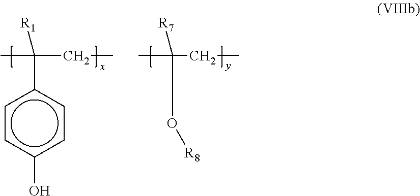


R1—(OCH═CH2)n (XII)
wherein R1 is selected from (C1-C30) linear, branched or cyclic alkyl, substituted or unsubstituted (C6-C40) aryl, or substituted or unsubstituted (C7-C40) alicyclic hydrocarbon; and n is an positive integer greater or equal to 2. Examples of such vinyl ether terminated crosslinking agents include bis(4-vinyloxy butyl) adipate; bis(4-vinyloxy butyl) succinate; bis(4-vinyloxy butyl) isophathalate; bis(4-vinyloxymethyl cyclohexylmethyl) glutarate; tris(4-vinyloxy butyl)trimellitate; bis(4-vinyloxy methyl cyclohexyl methyl) terephthalate; bis(4-vinyloxy methyl cyclohexyl methyl) isophthalate; bis(4-vinyloxy butyl) (4-methyl-1,3-phenylene)biscarbamate; bis(4-vinyloxy butyl)(methylene di-4,1-phenylene)biscarbamate; and triethyleneglycol divinylether, 1,4-cyclohexanedimentanol divinyl ether, various vinyl ether monomers available under the tradename Vectomer, such as, for example, 4-(vinyloxy)butyl benzoate, bis[4-(vinyloxy)butyl]adipate, bis[4-(vinyloxy)butyl]succinate, 4-(vinyloxymethyl)cyclohexylmethyl benzoate, bis[4-(vinyloxy)butyl]isophthalate, bis[4-(vinyloxymethyl)cyclohexylmethyl]glutarate, tris[4-(vinyloxy)butyl]trimellitate, 4-(vinyloxy)butyl stearate, bis[4-(vinyloxy)butyl]hexanediylbiscarbamate, bis[[4-[(vinyloxy)methyl]cyclohexyl]methyl]terephthalate, bis[[4-[(vinyloxy)methyl]cyclohexyl]methyl]isophthalate, bis[4-(vinyloxy)butyl](methylenedi-4,1-phenylene)biscarbamate, bis[4-(vinyloxy)butyl](4-methyl-1,3-phenylene)biscarbamate, and polymers bearing pendant vinyloxy groups. Other vinyl ether terminated crosslinking agents are described in T. Yamaoka, et al., Trends in Photochem. Photobio., 7:45 (2001); S. Moon, et al., Chem. Mater., 6:1854 (1994); or H. Schacht, et al., ACS Symp. Ser. 706:78 (1998), which may also be used and are incorporated herein by reference. In one embodiment the multifunctional vinyl ethers is 1,2,4-cyclohexyltricarboxylicacid-butylvinylester, also known by the systematic name tris[4-(vinyloxy)butyl]1,2,4-cyclohexyltricarboxylate (CHTA-BVE) of structure (XIII).

| TABLE 1a |
| Comparison of hydroxyl compounds of Structure (I) in |
| formulations with TSA for via filling at different temperatures |
| Tungstosilicic | 4-hydroxyphenyl | |||||
| acid, wt | compound | Coating | Coating | |||
| % Total | 4-hydroxyphenyl | Wt % Total | Quality at | Via Fill at | Quality at | Via Fill at |
| Solids | compound | Solids | 250° C./60 s | 250° C./60 s | 350° C./120 s | 350° C./120 s |
| 95 | PHSMMA | 5 | — | — | Hazy | — |
| 85 | PHSMMA | 15 | — | — | Good | voids |
| 80 | PHSMMA | 20 | — | — | Good | voids |
| 75 | PHSMMA | 25 | — | — | Good | voids |
| 70 | PHSMMA | 30 | — | — | Good | few voids |
| 67 | PHSMMA | 33 | Good | Bad | Good | Good |
| 65 | PHSMMA | 35 | Good | Bad | Good | Good |
| 55 | PHSMMA | 45 | Good | Bad | Good | Good |
| 95 | PHS | 5 | — | — | Hazy | — |
| 85 | PHS | 15 | — | — | Good | small voids at |
| bottom | ||||||
| 80 | PHS | 20 | — | — | Good | small voids at |
| bottom | ||||||
| 75 | PHS | 25 | Slightly | Bad | Good | Good |
| Rough | ||||||
| 65 | PHS | 35 | Good | Bad | Good | Good |
| 55 | PHS | 45 | Good | Bad | Good | Good |
| 95 | THTPM | 5 | Hazy | — | Hazy | N/A |
| 85 | THTPM | 15 | Slightly Hazy | — | Good | good but film |
| quality is bad | ||||||
| 80 | THTPM | 20 | Good | Good | Good | Good |
| 75 | THTPM | 25 | Good | Good | Good | Good |
| 65 | THTPM | 35 | Good | Good | Good | Good |
| 55 | THTPM | 45 | Good | Good | Good | Good |
| TABLE 1.b |
| Comparison of hydroxyl compounds not having Structure (I) in |
| formulations with TSA for via filling at different temperatures |
| Tungstosilicic | Hydroxyl | |||||
| acid, wt | Hydroxyl | compound, | Coating | |||
| % Total | compound | Wt % Total | Quality at | Via Fill at | Coating Quality | Via Fill at |
| Solids | name | Solids | 250° C./60 sec | 250° C./60 s | at 350° C./120 s | 350° C./120 s |
| 80 | PAA | 20 | Hazy | — | Hazy | — |
| 75 | PAA | 25 | Hazy | Bad | Good | Voids |
| 65 | PAA | 35 | Good | Bad | Good | Voids |
| 75 | NP | 25 | Hazy | Bad | Hazy | Voids |
| 65 | NP | 35 | Hazy | Bad | Hazy | Voids |
| 75 | DHBP | 25 | Hazy | Bad | Hazy | Voids |
| 65 | DHBP | 35 | Hazy | Bad | Hazy | Voids |
| 75 | B2N | 25 | Hazy | Bad | Hazy | Voids |
| 65 | B2N | 35 | Hazy | Bad | Hazy | Voids |
| 80 | SPN-560 | 20 | — | — | Hazy | — |
| 75 | SPN-560 | 25 | Hazy, cracked | — | Hazy, cracked | — |
| film | film | |||||
| 66.6 | SPN-560 | 33.3 | Hazy, cracked | — | Hazy, cracked | — |
| film | film | |||||
Refractive Index:
| TABLE 2 |
| Film thickness change at different bake temperatures |
| Film | Film | |||||
| RTA | Shrinkage | Film | Shrinkage | |||
| (Rapid | after holding | Shrinkaqe | after holding | |||
| Organic | Thermal | RTA | for | after holding | for | |
| Additive | Annealing) | Temp | 2 min | for | 10 min | |
| to TSA | Bake Process | Chamber | Profile in N2 | @600° C. | 5 min @600° C. | @600° C. |
| PHSMMA | 250° C./60 s + | Vacuum | Ramp-up to | 18% | 18% | 13% |
| 350° C./60 s | 600° C. | |||||
| 350° C./120 s | 18% | 18% | 10% | |||
| PHS | 350° C./120 s | 15% | 17% | 7% | ||
| THTPM | 250° C./60 s + | 15% | 13% | 10% | ||
| 350° C./60 s | ||||||
| 350° C./120 s | 11% | 14% | 0% | |||
| TABLE 3 |
| Detailed RTA Recipe |
| Under | Recipe | Time | Rate | ||
| Vacuum | vacuum (AP → 1.0 Pa) | 30 sec | |||
| Hold | 30 sec | ||||
| Ramp-up | 6 min | 100° C./min | |||
| Hold | 2 min | — | |||
| Cooling | 10 min | 30° C./min | |||
| N2 | N2 blow (1.0 Pa → AP) | 30 sec | |||
Etch Rate for Coatings Prepared Based on Formulation and Coating
Coating Example 2a in CHF3 and O2/Ar Etch Gasses
| TABLE 4 | |||
| RF POWER | 500 W (ISM)/250 | RF POWER | 700 W (ISM)/200 |
| W (Bias) | W (Bias) | ||
| Gas Flow | CHF3 = 50 sccm | Gas Flow | O2/Ar = 30/25 sccm |
| Pressure | 20 mTorr | Pressure | 30 mTorr |
| Etching Time | 30 sec | Etching Time | 300 sec |
| Back He Temp | 20° C. | Back He Temp | 20° C. |
| TABLE 5 | ||
| Selectivity | ||
| Etch rate | Etch rate ratio | ||
| ratio of resist | of U98 etch | ||
| Etch rate | to different | to different | |
| (nm/min) | Materials | materials |
| Material | CHF3 | O2/Ar | CHF3 | O2/Ar | CHF3 | O2/Ar |
| AX2110P | 154 | 1057.1 | 1.00 | 1.00 | 0.46 | 0.70 |
| Thermal Oxide | 118.4 | 2.7 | 1.30 | 392 | 0.60 | 275 |
| U98 | 70.7 | 742.8 | 2.18 | 1.42 | 1.00 | 1.00 |
| Formulation 2 | 155.1 | 10 | 0.99 | 106 | 0.46 | 74.00 |
| (PHSMMA) | ||||||
| TABLE 6 |
| Crosslinking agents |
| Final after | Final | ||||||
| ArF- | after AZ | ||||||
| Initial, | Thinner | Change | 300 MIF | % | |||
| Composition | °A | soak, °A | (°A) | % loss | soak, °A | Change | loss |
| 75% TSA, 25% PHSMMA, 15% | 3095 | 3120 | 25 | 0.80775 | 3167 | 72 | 2.32633 |
| TMOM-BP, 2% DBSA/E, 100% | |||||||
| PGMEA/PGME solvent | |||||||
| 75% TSA, 25% PHSMMA, 15% | 2807.5 | 2877.5 | 70 | 2.49332 | 2992.5 | 185 | 6.589 |
| XL-CHTA-BVEx-linker, 2% | |||||||
| DBSA/E, 100% PGMEA/PGME | |||||||
| solvent | |||||||
Summary of Unexpected Results
Claims (14)


Priority Applications (15)
| Application Number | Priority Date | Filing Date | Title |
|---|---|---|---|
| US14/154,929 US9409793B2 (en) | 2014-01-14 | 2014-01-14 | Spin coatable metallic hard mask compositions and processes thereof |
| US14/445,757 US9418836B2 (en) | 2014-01-14 | 2014-07-29 | Polyoxometalate and heteropolyoxometalate compositions and methods for their use |
| EP20199538.8A EP3812839B1 (en) | 2014-01-14 | 2014-12-08 | Polyoxometalate and heteropolyoxometalate compositions and method using them |
| KR1020167022066A KR101833159B1 (en) | 2014-01-14 | 2014-12-08 | Polyoxometalate and heteropolyoxometalate compositions and methods for their use |
| KR1020177029583A KR102123144B1 (en) | 2014-01-14 | 2014-12-08 | Polyoxometalate and heteropolyoxometalate compositions and methods for their use |
| SG10201608338PA SG10201608338PA (en) | 2014-01-14 | 2014-12-08 | Polyoxometalate and heteropolyoxometalate compositions and methods for their use |
| JP2016546495A JP6316441B2 (en) | 2014-01-14 | 2014-12-08 | Polyoxometalate and heteropolyoxometalate compositions and methods of use thereof |
| CN201480072379.5A CN105900014B (en) | 2014-01-14 | 2014-12-08 | Polyoxometallate and heteropolyoxometallate composition and its application method |
| EP17188465.3A EP3276416A1 (en) | 2014-01-14 | 2014-12-08 | Method for generating nanorods arrays using polyoxometalate and heteropolyoxometalate compositions |
| CN201910902154.2A CN110609445B (en) | 2014-01-14 | 2014-12-08 | Polyoxometalate and heteropolyoxometalate compositions and methods of use thereof |
| PCT/EP2014/076919 WO2015106885A1 (en) | 2014-01-14 | 2014-12-08 | Polyoxometalate and heteropolyoxometalate compositions and methods for their use |
| EP14809018.6A EP3095008B1 (en) | 2014-01-14 | 2014-12-08 | Polyoxometalate and heteropolyoxometalate compositions and process for forming a negative tone image |
| TW106110598A TWI637033B (en) | 2014-01-14 | 2015-01-14 | Polyoxometalate and heteropolyoxometalate compositions and methods for their use |
| TW104101241A TWI600730B (en) | 2014-01-14 | 2015-01-14 | Polyoxometalate and heteropolyoxometalate compositions and methods for their use |
| IL246383A IL246383A0 (en) | 2014-01-14 | 2016-06-22 | Polyoxometalate and heteropolyoxometalate compositions and methods for their use |
Applications Claiming Priority (1)
| Application Number | Priority Date | Filing Date | Title |
|---|---|---|---|
| US14/154,929 US9409793B2 (en) | 2014-01-14 | 2014-01-14 | Spin coatable metallic hard mask compositions and processes thereof |
Related Child Applications (1)
| Application Number | Title | Priority Date | Filing Date |
|---|---|---|---|
| US14/445,757 Continuation-In-Part US9418836B2 (en) | 2014-01-14 | 2014-07-29 | Polyoxometalate and heteropolyoxometalate compositions and methods for their use |
Publications (2)
| Publication Number | Publication Date |
|---|---|
| US20150200090A1 US20150200090A1 (en) | 2015-07-16 |
| US9409793B2 true US9409793B2 (en) | 2016-08-09 |
Family
ID=53521951
Family Applications (1)
| Application Number | Title | Priority Date | Filing Date |
|---|---|---|---|
| US14/154,929 Active 2034-03-17 US9409793B2 (en) | 2014-01-14 | 2014-01-14 | Spin coatable metallic hard mask compositions and processes thereof |
Country Status (1)
| Country | Link |
|---|---|
| US (1) | US9409793B2 (en) |
Cited By (2)
| Publication number | Priority date | Publication date | Assignee | Title |
|---|---|---|---|---|
| WO2018167112A1 (en) | 2017-03-16 | 2018-09-20 | Merck Patent Gmbh | Lithographic compositions and methods of use thereof |
| WO2021004985A1 (en) | 2019-07-08 | 2021-01-14 | Merck Patent Gmbh | Rinse and method of use thereof for removing edge protection layers and residual metal hardmask components |
Families Citing this family (11)
| Publication number | Priority date | Publication date | Assignee | Title |
|---|---|---|---|---|
| US9201305B2 (en) | 2013-06-28 | 2015-12-01 | Az Electronic Materials (Luxembourg) S.A.R.L. | Spin-on compositions of soluble metal oxide carboxylates and methods of their use |
| US9418836B2 (en) * | 2014-01-14 | 2016-08-16 | Az Electronic Materials (Luxembourg) S.A.R.L. | Polyoxometalate and heteropolyoxometalate compositions and methods for their use |
| US9583358B2 (en) | 2014-05-30 | 2017-02-28 | Samsung Electronics Co., Ltd. | Hardmask composition and method of forming pattern by using the hardmask composition |
| KR102287343B1 (en) | 2014-07-04 | 2021-08-06 | 삼성전자주식회사 | Hardmask composition and method of forming patterning using the hardmask composition |
| KR102287344B1 (en) * | 2014-07-25 | 2021-08-06 | 삼성전자주식회사 | Hardmask composition and method of forming patterning using the hardmask composition |
| KR102384226B1 (en) | 2015-03-24 | 2022-04-07 | 삼성전자주식회사 | Hardmask composition and method of forming pattern using the same |
| KR102463893B1 (en) | 2015-04-03 | 2022-11-04 | 삼성전자주식회사 | Hardmask composition and method of forming patterning using the hardmask composition |
| JP2017090849A (en) * | 2015-11-17 | 2017-05-25 | アーゼッド・エレクトロニック・マテリアルズ(ルクセンブルグ)ソシエテ・ア・レスポンサビリテ・リミテ | High heat-resistant resist composition and pattern forming method using the same |
| US11034847B2 (en) | 2017-07-14 | 2021-06-15 | Samsung Electronics Co., Ltd. | Hardmask composition, method of forming pattern using hardmask composition, and hardmask formed from hardmask composition |
| KR102433666B1 (en) | 2017-07-27 | 2022-08-18 | 삼성전자주식회사 | Hardmask composition, method of forming patterning using the hardmask composition, and hardmask formed from the hardmask composition |
| KR102486388B1 (en) | 2017-07-28 | 2023-01-09 | 삼성전자주식회사 | Method of preparing graphene quantum dot, hardmask composition including the graphene quantum dot obtained by the method, method of forming patterning using the hardmask composition, and hardmask formed from the hardmask composition |
Citations (72)
| Publication number | Priority date | Publication date | Assignee | Title |
|---|---|---|---|---|
| US3474054A (en) | 1966-09-13 | 1969-10-21 | Permalac Corp The | Surface coating compositions containing pyridine salts or aromatic sulfonic acids |
| US4200729A (en) | 1978-05-22 | 1980-04-29 | King Industries, Inc | Curing amino resins with aromatic sulfonic acid oxa-azacyclopentane adducts |
| US4251665A (en) | 1978-05-22 | 1981-02-17 | King Industries, Inc. | Aromatic sulfonic acid oxa-azacyclopentane adducts |
| US4491628A (en) | 1982-08-23 | 1985-01-01 | International Business Machines Corporation | Positive- and negative-working resist compositions with acid generating photoinitiator and polymer with acid labile groups pendant from polymer backbone |
| JPS6356529A (en) | 1986-08-27 | 1988-03-11 | Nissan Chem Ind Ltd | Novel titanosiloxane polymer and production thereof |
| WO1991001516A2 (en) | 1989-07-21 | 1991-02-07 | Board Of Regents, The University Of Texas System | Pattern forming and transferring processes |
| JPH03138922A (en) | 1989-10-24 | 1991-06-13 | Matsushita Electric Ind Co Ltd | Minute-pattern forming method |
| US5187019A (en) | 1991-09-06 | 1993-02-16 | King Industries, Inc. | Latent catalysts |
| JPH0632756A (en) * | 1992-07-14 | 1994-02-08 | Ube Ind Ltd | Production of bis@(3754/24)hydroxyphenyl)methanes |
| US5292558A (en) * | 1991-08-08 | 1994-03-08 | University Of Texas At Austin, Texas | Process for metal deposition for microelectronic interconnections |
| US5350660A (en) | 1990-01-30 | 1994-09-27 | Wako Pure Chemical Industries, Ltd. | Chemical amplified resist material containing photosensitive compound capable of generating an acid and specific polystyrene copolymer having functional groups that become alkali-soluble under an acid atmosphere |
| US5512417A (en) * | 1994-02-14 | 1996-04-30 | Shin-Etsu Chemical Co., Ltd. | Positive resist composition comprising a bis (t-butoxycarbonylmethly(thymolphthalein as a dissolution inhibitor |
| US5772978A (en) | 1996-04-24 | 1998-06-30 | Minnesota Mining And Manufacturing Company | Process for producing tungsten oxide |
| US5843624A (en) | 1996-03-08 | 1998-12-01 | Lucent Technologies Inc. | Energy-sensitive resist material and a process for device fabrication using an energy-sensitive resist material |
| US5879859A (en) | 1997-07-16 | 1999-03-09 | International Business Machines Corporation | Strippable photoimageable compositions |
| JP2000010293A (en) | 1998-06-17 | 2000-01-14 | Jsr Corp | Composition for forming antireflection film and antireflection film |
| US6242156B1 (en) | 2000-06-28 | 2001-06-05 | Gary Ganghui Teng | Lithographic plate having a conformal radiation-sensitive layer on a rough substrate |
| US6348299B1 (en) | 1999-07-12 | 2002-02-19 | International Business Machines Corporation | RIE etch resistant nonchemically amplified resist composition and use thereof |
| US6447980B1 (en) | 2000-07-19 | 2002-09-10 | Clariant Finance (Bvi) Limited | Photoresist composition for deep UV and process thereof |
| WO2003073164A2 (en) | 2002-02-27 | 2003-09-04 | Brewer Science, Inc. | Novel planarization method for multi-layer lithography processing |
| US20030235786A1 (en) | 2002-06-25 | 2003-12-25 | Brewer Science, Inc. | Developer-soluble metal alkoxide coatings for microelectronic applications |
| US20040058275A1 (en) | 2002-06-25 | 2004-03-25 | Brewer Science, Inc. | Wet-developable anti-reflective compositions |
| US6723488B2 (en) | 2001-11-07 | 2004-04-20 | Clariant Finance (Bvi) Ltd | Photoresist composition for deep UV radiation containing an additive |
| US20040102048A1 (en) | 2002-11-25 | 2004-05-27 | Renesas Technology Corp. | Method for manufacturing semiconductor device |
| US6790587B1 (en) | 1999-05-04 | 2004-09-14 | E. I. Du Pont De Nemours And Company | Fluorinated polymers, photoresists and processes for microlithography |
| US20040181031A1 (en) * | 2003-03-14 | 2004-09-16 | Nippon Shokubai Co., Ltd. | Surface crosslinking treatment method of water-absorbing resin powder |
| US20040224616A1 (en) * | 2003-04-25 | 2004-11-11 | Jsr Corporation | Polishing pad and chemical mechanical polishing method |
| US6818258B2 (en) | 2001-02-09 | 2004-11-16 | Asahi Glass Company, Limited | Resist composition |
| US6849377B2 (en) | 1998-09-23 | 2005-02-01 | E. I. Du Pont De Nemours And Company | Photoresists, polymers and processes for microlithography |
| US6866984B2 (en) | 1996-12-31 | 2005-03-15 | Hyundai Electronics Industries Co., Ltd. | ArF photoresist copolymers |
| US6916590B2 (en) | 2000-06-21 | 2005-07-12 | Asahi Glass Company, Limited | Resist composition |
| US20050164133A1 (en) | 2000-10-24 | 2005-07-28 | Advanced Micro Devices, Inc. | Inverse resist coating process |
| JP2005307101A (en) * | 2004-04-26 | 2005-11-04 | Taiyo Ink Mfg Ltd | Thermosetting resin composition |
| JP2006098284A (en) | 2004-09-30 | 2006-04-13 | National Institute Of Advanced Industrial & Technology | Mesoporous metal oxide complex glass waveguiding layer sensor, its manufacturing method, and gas sensor using it |
| US20060263708A1 (en) | 2005-05-20 | 2006-11-23 | Xerox Corporation | Imaging member |
| US20070015083A1 (en) | 2005-07-14 | 2007-01-18 | International Business Machines Corporation | Antireflective composition and process of making a lithographic structure |
| JP2007061720A (en) | 2005-08-30 | 2007-03-15 | Niigata Univ | Photocatalyst membrane and its manufacturing method |
| US20070116640A1 (en) | 2005-06-16 | 2007-05-24 | Korea Institute Of Science And Technology | Titanium dioxide nanorod and preparation method thereof |
| US20070134916A1 (en) | 2005-12-14 | 2007-06-14 | Shin-Etsu Chemical Co., Ltd. | Antireflection film composition, patterning process and substrate using the same |
| US20070224483A1 (en) | 2004-04-30 | 2007-09-27 | Giulio Alberti | Presursor Organic of Tetravalent Metal Phosphates and Pyrophosphates and Their Use for Electrode Modification and for the Preparation of Composite Membrane for Fuel Cells Working at Temperatures>90c and / or at Low Relative Humidity |
| US20070243473A1 (en) | 2004-05-11 | 2007-10-18 | Tetsuro Mizushima | Hologram Recording Material and Hologram Recording Medium |
| US20080039542A1 (en) * | 2006-08-11 | 2008-02-14 | General Electric Company | Composition and associated method |
| US20080044764A1 (en) * | 2003-11-25 | 2008-02-21 | Toru Takahashi | Chemically Amplified Positive Photosensitive Thermosetting Resin Composition, Method Of Forming Cured Article, And Method Of Producing Functional Device |
| US20080076064A1 (en) | 2006-09-25 | 2008-03-27 | Sun Sam X | Method of creating photolithographic structures with developer-trimmed hard mask |
| US7416834B2 (en) | 2006-09-27 | 2008-08-26 | Az Electronic Materials Usa Corp. | Antireflective coating compositions |
| US20090239080A1 (en) * | 2006-08-29 | 2009-09-24 | Jsr Corporation | Photosensitive insulation resin composition and cured product thereof |
| US20090286188A1 (en) | 2008-05-15 | 2009-11-19 | Shin-Etsu Chemical Co., Ltd. | Patterning process |
| US20100028804A1 (en) | 2008-08-04 | 2010-02-04 | Fujifilm Corporation | Resist composition and method of forming pattern therewith |
| US20100099044A1 (en) | 2008-10-20 | 2010-04-22 | Shin-Etsu Chemical Co.,Ltd. | Method for forming resist underlayer film, patterning process using the same, and composition for the resist underlayer film |
| US20100130697A1 (en) * | 2005-09-13 | 2010-05-27 | Atsuhiko Katayama | Thermosetting Resin Composition |
| US7727902B2 (en) | 2003-12-26 | 2010-06-01 | Nissan Chemical Industries, Ltd. | Composition for forming nitride coating film for hard mask |
| US7767368B2 (en) | 2006-09-25 | 2010-08-03 | Shin-Etsu Chemical Co., Ltd. | Method of fabricating photomask blank |
| US7799396B2 (en) | 2005-06-03 | 2010-09-21 | Kuraray Co., Ltd. | Gas barrier layered product, method of manufacturing the same and packaging medium using the same |
| US7803458B2 (en) | 2003-01-21 | 2010-09-28 | Brewer Science Inc. | Hybrid organic-inorganic polymer coatings with high refractive indices |
| US20110081615A1 (en) | 2008-08-20 | 2011-04-07 | Fujitsu Limited | Material for forming resist sensitization film and production method of semiconductor device |
| US20110207864A1 (en) | 2008-10-23 | 2011-08-25 | Mie University | Polyorganosiloxane composition and cured production thereof |
| US8039201B2 (en) | 2007-11-21 | 2011-10-18 | Az Electronic Materials Usa Corp. | Antireflective coating composition and process thereof |
| US20120108071A1 (en) | 2010-11-01 | 2012-05-03 | Shin-Etsu Chemical Co., Ltd. | Resist underlayer film composition and patterning process using the same |
| US20120178261A1 (en) | 2009-09-16 | 2012-07-12 | Nissan Chemical Industries, Ltd. | Silicon-containing composition having sulfonamide group for forming resist underlayer film |
| EP2477775A1 (en) | 2009-09-16 | 2012-07-25 | Wilhelm Altendorf GmbH & Co. KG | Circular final trimming saw having direct drive |
| WO2012099134A1 (en) * | 2011-01-18 | 2012-07-26 | 日立化成工業株式会社 | Resin composition, and printed wiring board, laminated sheet, and prepreg using same |
| US20120223418A1 (en) | 2011-02-28 | 2012-09-06 | Stowers Jason K | Solution processible hardmasks for high resolution lithography |
| US20120264039A1 (en) | 2009-10-14 | 2012-10-18 | Fujifilm Corporation | Colored curable composition, resist liquid, ink for inkjet printing, color filter, method of producing color filter, solid-state image sensor, liquid crystal display, organic el display, image display device and colorant compound |
| US20120288300A1 (en) | 2011-05-10 | 2012-11-15 | Konica Minolta Business Technologies, Inc. | Electrophotographic photoconductor, process cartridge including the same, and image forming apparatus including the same |
| US20120328990A1 (en) | 2011-06-21 | 2012-12-27 | Az Electronic Materials Usa Corp. | Underlayer composition and process thereof |
| US20130040140A1 (en) | 2010-02-15 | 2013-02-14 | Cornell University | Electrospinning apparatus and nanofibers produced therefrom |
| US20130123137A1 (en) | 2010-06-22 | 2013-05-16 | CENTRO DE INVESTIGACIÓN COOPERATIVA EN BIOMATERIALS (CIC biomaGUNE) | Method for the characterization of intermolecular interactions |
| US20140159278A1 (en) | 2012-12-07 | 2014-06-12 | Az Electronic Materials (Luxembourg) S.A.R.L. | Stable metal compounds, their compositions and methods |
| US20140356792A1 (en) | 2011-08-11 | 2014-12-04 | Az Electronic Materials Usa Corp. | Composition for forming tungsten oxide film and method for producing tungsten oxide film using same |
| US20150004801A1 (en) | 2013-06-28 | 2015-01-01 | Az Electronic Materials (Luxembourg) S.A.R.L. | Spin-on compositions of soluble metal oxide carboxylates and methods of their use |
| US20150064904A1 (en) | 2013-08-30 | 2015-03-05 | Az Electronic Materials (Luxembourg) S.A.R.L. | Stable metal compounds as hardmasks and filling materials, their compositions and methods of use |
| US20150200091A1 (en) * | 2014-01-14 | 2015-07-16 | Az Electronic Materials (Luxembourg) S.A.R.L. | Polyoxometalate and heteropolyoxometalate compositions and methods for their use |
-
2014
- 2014-01-14 US US14/154,929 patent/US9409793B2/en active Active
Patent Citations (75)
| Publication number | Priority date | Publication date | Assignee | Title |
|---|---|---|---|---|
| US3474054A (en) | 1966-09-13 | 1969-10-21 | Permalac Corp The | Surface coating compositions containing pyridine salts or aromatic sulfonic acids |
| US4200729A (en) | 1978-05-22 | 1980-04-29 | King Industries, Inc | Curing amino resins with aromatic sulfonic acid oxa-azacyclopentane adducts |
| US4251665A (en) | 1978-05-22 | 1981-02-17 | King Industries, Inc. | Aromatic sulfonic acid oxa-azacyclopentane adducts |
| US4491628A (en) | 1982-08-23 | 1985-01-01 | International Business Machines Corporation | Positive- and negative-working resist compositions with acid generating photoinitiator and polymer with acid labile groups pendant from polymer backbone |
| JPS6356529A (en) | 1986-08-27 | 1988-03-11 | Nissan Chem Ind Ltd | Novel titanosiloxane polymer and production thereof |
| US5178989A (en) * | 1989-07-21 | 1993-01-12 | Board Of Regents, The University Of Texas System | Pattern forming and transferring processes |
| WO1991001516A2 (en) | 1989-07-21 | 1991-02-07 | Board Of Regents, The University Of Texas System | Pattern forming and transferring processes |
| JPH03138922A (en) | 1989-10-24 | 1991-06-13 | Matsushita Electric Ind Co Ltd | Minute-pattern forming method |
| US5350660A (en) | 1990-01-30 | 1994-09-27 | Wako Pure Chemical Industries, Ltd. | Chemical amplified resist material containing photosensitive compound capable of generating an acid and specific polystyrene copolymer having functional groups that become alkali-soluble under an acid atmosphere |
| US5292558A (en) * | 1991-08-08 | 1994-03-08 | University Of Texas At Austin, Texas | Process for metal deposition for microelectronic interconnections |
| US5187019A (en) | 1991-09-06 | 1993-02-16 | King Industries, Inc. | Latent catalysts |
| JPH0632756A (en) * | 1992-07-14 | 1994-02-08 | Ube Ind Ltd | Production of bis@(3754/24)hydroxyphenyl)methanes |
| US5512417A (en) * | 1994-02-14 | 1996-04-30 | Shin-Etsu Chemical Co., Ltd. | Positive resist composition comprising a bis (t-butoxycarbonylmethly(thymolphthalein as a dissolution inhibitor |
| US5843624A (en) | 1996-03-08 | 1998-12-01 | Lucent Technologies Inc. | Energy-sensitive resist material and a process for device fabrication using an energy-sensitive resist material |
| US5772978A (en) | 1996-04-24 | 1998-06-30 | Minnesota Mining And Manufacturing Company | Process for producing tungsten oxide |
| US6866984B2 (en) | 1996-12-31 | 2005-03-15 | Hyundai Electronics Industries Co., Ltd. | ArF photoresist copolymers |
| US5879859A (en) | 1997-07-16 | 1999-03-09 | International Business Machines Corporation | Strippable photoimageable compositions |
| JP2000010293A (en) | 1998-06-17 | 2000-01-14 | Jsr Corp | Composition for forming antireflection film and antireflection film |
| US6849377B2 (en) | 1998-09-23 | 2005-02-01 | E. I. Du Pont De Nemours And Company | Photoresists, polymers and processes for microlithography |
| US6790587B1 (en) | 1999-05-04 | 2004-09-14 | E. I. Du Pont De Nemours And Company | Fluorinated polymers, photoresists and processes for microlithography |
| US6348299B1 (en) | 1999-07-12 | 2002-02-19 | International Business Machines Corporation | RIE etch resistant nonchemically amplified resist composition and use thereof |
| US6916590B2 (en) | 2000-06-21 | 2005-07-12 | Asahi Glass Company, Limited | Resist composition |
| US6242156B1 (en) | 2000-06-28 | 2001-06-05 | Gary Ganghui Teng | Lithographic plate having a conformal radiation-sensitive layer on a rough substrate |
| US6447980B1 (en) | 2000-07-19 | 2002-09-10 | Clariant Finance (Bvi) Limited | Photoresist composition for deep UV and process thereof |
| US20050164133A1 (en) | 2000-10-24 | 2005-07-28 | Advanced Micro Devices, Inc. | Inverse resist coating process |
| US6818258B2 (en) | 2001-02-09 | 2004-11-16 | Asahi Glass Company, Limited | Resist composition |
| US6723488B2 (en) | 2001-11-07 | 2004-04-20 | Clariant Finance (Bvi) Ltd | Photoresist composition for deep UV radiation containing an additive |
| WO2003073164A2 (en) | 2002-02-27 | 2003-09-04 | Brewer Science, Inc. | Novel planarization method for multi-layer lithography processing |
| US20040058275A1 (en) | 2002-06-25 | 2004-03-25 | Brewer Science, Inc. | Wet-developable anti-reflective compositions |
| US20030235786A1 (en) | 2002-06-25 | 2003-12-25 | Brewer Science, Inc. | Developer-soluble metal alkoxide coatings for microelectronic applications |
| US20040102048A1 (en) | 2002-11-25 | 2004-05-27 | Renesas Technology Corp. | Method for manufacturing semiconductor device |
| US7803458B2 (en) | 2003-01-21 | 2010-09-28 | Brewer Science Inc. | Hybrid organic-inorganic polymer coatings with high refractive indices |
| US20040181031A1 (en) * | 2003-03-14 | 2004-09-16 | Nippon Shokubai Co., Ltd. | Surface crosslinking treatment method of water-absorbing resin powder |
| US20040224616A1 (en) * | 2003-04-25 | 2004-11-11 | Jsr Corporation | Polishing pad and chemical mechanical polishing method |
| US20080044764A1 (en) * | 2003-11-25 | 2008-02-21 | Toru Takahashi | Chemically Amplified Positive Photosensitive Thermosetting Resin Composition, Method Of Forming Cured Article, And Method Of Producing Functional Device |
| US7727902B2 (en) | 2003-12-26 | 2010-06-01 | Nissan Chemical Industries, Ltd. | Composition for forming nitride coating film for hard mask |
| JP2005307101A (en) * | 2004-04-26 | 2005-11-04 | Taiyo Ink Mfg Ltd | Thermosetting resin composition |
| US20070224483A1 (en) | 2004-04-30 | 2007-09-27 | Giulio Alberti | Presursor Organic of Tetravalent Metal Phosphates and Pyrophosphates and Their Use for Electrode Modification and for the Preparation of Composite Membrane for Fuel Cells Working at Temperatures>90c and / or at Low Relative Humidity |
| US20070243473A1 (en) | 2004-05-11 | 2007-10-18 | Tetsuro Mizushima | Hologram Recording Material and Hologram Recording Medium |
| JP2006098284A (en) | 2004-09-30 | 2006-04-13 | National Institute Of Advanced Industrial & Technology | Mesoporous metal oxide complex glass waveguiding layer sensor, its manufacturing method, and gas sensor using it |
| US20060263708A1 (en) | 2005-05-20 | 2006-11-23 | Xerox Corporation | Imaging member |
| US7799396B2 (en) | 2005-06-03 | 2010-09-21 | Kuraray Co., Ltd. | Gas barrier layered product, method of manufacturing the same and packaging medium using the same |
| US20070116640A1 (en) | 2005-06-16 | 2007-05-24 | Korea Institute Of Science And Technology | Titanium dioxide nanorod and preparation method thereof |
| US20070015083A1 (en) | 2005-07-14 | 2007-01-18 | International Business Machines Corporation | Antireflective composition and process of making a lithographic structure |
| JP2007061720A (en) | 2005-08-30 | 2007-03-15 | Niigata Univ | Photocatalyst membrane and its manufacturing method |
| US20100130697A1 (en) * | 2005-09-13 | 2010-05-27 | Atsuhiko Katayama | Thermosetting Resin Composition |
| US20070134916A1 (en) | 2005-12-14 | 2007-06-14 | Shin-Etsu Chemical Co., Ltd. | Antireflection film composition, patterning process and substrate using the same |
| US20080039542A1 (en) * | 2006-08-11 | 2008-02-14 | General Electric Company | Composition and associated method |
| US20090239080A1 (en) * | 2006-08-29 | 2009-09-24 | Jsr Corporation | Photosensitive insulation resin composition and cured product thereof |
| US7767368B2 (en) | 2006-09-25 | 2010-08-03 | Shin-Etsu Chemical Co., Ltd. | Method of fabricating photomask blank |
| US20080076064A1 (en) | 2006-09-25 | 2008-03-27 | Sun Sam X | Method of creating photolithographic structures with developer-trimmed hard mask |
| US7416834B2 (en) | 2006-09-27 | 2008-08-26 | Az Electronic Materials Usa Corp. | Antireflective coating compositions |
| US8039201B2 (en) | 2007-11-21 | 2011-10-18 | Az Electronic Materials Usa Corp. | Antireflective coating composition and process thereof |
| US20090286188A1 (en) | 2008-05-15 | 2009-11-19 | Shin-Etsu Chemical Co., Ltd. | Patterning process |
| US20100028804A1 (en) | 2008-08-04 | 2010-02-04 | Fujifilm Corporation | Resist composition and method of forming pattern therewith |
| US20110081615A1 (en) | 2008-08-20 | 2011-04-07 | Fujitsu Limited | Material for forming resist sensitization film and production method of semiconductor device |
| US20100099044A1 (en) | 2008-10-20 | 2010-04-22 | Shin-Etsu Chemical Co.,Ltd. | Method for forming resist underlayer film, patterning process using the same, and composition for the resist underlayer film |
| US20110207864A1 (en) | 2008-10-23 | 2011-08-25 | Mie University | Polyorganosiloxane composition and cured production thereof |
| US20120178261A1 (en) | 2009-09-16 | 2012-07-12 | Nissan Chemical Industries, Ltd. | Silicon-containing composition having sulfonamide group for forming resist underlayer film |
| EP2477775A1 (en) | 2009-09-16 | 2012-07-25 | Wilhelm Altendorf GmbH & Co. KG | Circular final trimming saw having direct drive |
| US20120264039A1 (en) | 2009-10-14 | 2012-10-18 | Fujifilm Corporation | Colored curable composition, resist liquid, ink for inkjet printing, color filter, method of producing color filter, solid-state image sensor, liquid crystal display, organic el display, image display device and colorant compound |
| US20130040140A1 (en) | 2010-02-15 | 2013-02-14 | Cornell University | Electrospinning apparatus and nanofibers produced therefrom |
| US20130123137A1 (en) | 2010-06-22 | 2013-05-16 | CENTRO DE INVESTIGACIÓN COOPERATIVA EN BIOMATERIALS (CIC biomaGUNE) | Method for the characterization of intermolecular interactions |
| US20120108071A1 (en) | 2010-11-01 | 2012-05-03 | Shin-Etsu Chemical Co., Ltd. | Resist underlayer film composition and patterning process using the same |
| WO2012099134A1 (en) * | 2011-01-18 | 2012-07-26 | 日立化成工業株式会社 | Resin composition, and printed wiring board, laminated sheet, and prepreg using same |
| US20140000948A1 (en) * | 2011-01-18 | 2014-01-02 | Shunsuke Nagai | Resin composition, and printed wiring board, laminated sheet, and prepreg using same |
| US20120223418A1 (en) | 2011-02-28 | 2012-09-06 | Stowers Jason K | Solution processible hardmasks for high resolution lithography |
| US20120288300A1 (en) | 2011-05-10 | 2012-11-15 | Konica Minolta Business Technologies, Inc. | Electrophotographic photoconductor, process cartridge including the same, and image forming apparatus including the same |
| US8568958B2 (en) | 2011-06-21 | 2013-10-29 | Az Electronic Materials Usa Corp. | Underlayer composition and process thereof |
| US20120328990A1 (en) | 2011-06-21 | 2012-12-27 | Az Electronic Materials Usa Corp. | Underlayer composition and process thereof |
| US20140356792A1 (en) | 2011-08-11 | 2014-12-04 | Az Electronic Materials Usa Corp. | Composition for forming tungsten oxide film and method for producing tungsten oxide film using same |
| US20140159278A1 (en) | 2012-12-07 | 2014-06-12 | Az Electronic Materials (Luxembourg) S.A.R.L. | Stable metal compounds, their compositions and methods |
| US20150004801A1 (en) | 2013-06-28 | 2015-01-01 | Az Electronic Materials (Luxembourg) S.A.R.L. | Spin-on compositions of soluble metal oxide carboxylates and methods of their use |
| US20150064904A1 (en) | 2013-08-30 | 2015-03-05 | Az Electronic Materials (Luxembourg) S.A.R.L. | Stable metal compounds as hardmasks and filling materials, their compositions and methods of use |
| US20150200091A1 (en) * | 2014-01-14 | 2015-07-16 | Az Electronic Materials (Luxembourg) S.A.R.L. | Polyoxometalate and heteropolyoxometalate compositions and methods for their use |
Non-Patent Citations (33)
| Title |
|---|
| "Alkyienes", PAC, 1995, 67, 1307, (Glossary of class names of organice compounds and reactivity intermediates based on structure (IUPAC Recommendations 1995) on p. 1314, obtained from hhtp://goldbook.iupac.org/!00227-plain.html on Mar. 11, 2013. |
| A. Scroggie et al., "The Crystal Structure of Anhydrous Silicotungstic Acid and Related Compounds, and Their Probable Molecular Formulas," Proceedings of the National Academy of Sciences vol. 15, No. 1, pp. 1-pp. 8 (1929). |
| Baxendale et al., "The Reduction of Molybdenum(ll) Trifluoroacetate by Pulse Radiolysis in Methanols", Journal of the American Chemical Society vol. 98 No. 2, pp. 637-pp. 638 (1976). |
| Burch et al., "Scrambling of Fluoro-, Methoxyl, Dimethylamino-, and Methyl Gropus with Chlorine Atoms of Methoxyl with Dimethylaminal-Groups Germanium", J. Chm. Soc. (A), pp. 586-pp. 589 (1966). |
| D. Abdallah et al., "Image Reversal Trilayer Process Using Standard Positive Photoresist", SPIE vol. 7273, No. 72732K, pp. 72732K-1-pp. 72732K-9 (2009). |
| D. Bajuk-Bogdanovic, "A Study of 12-tungstosilicic acid and 12-molybdophosphoric acids in solution," Journal of the Serbian Chemical Society vol. 73(2), pp. 197-pp. 209 (2008). |
| English Translation of Notification of the First Office Action dated Sep. 1, 2014 from the Chinese Patent Office for CN2012800262639, which corresponds to U.S. Appl. No. 13/164,869. |
| Form PCT/IB/326, Form PCT/IB/373, and Form PCT/ISA/237 for PCT/IB2012/001219 dated Jan. 9, 2014, which corresponds to U.S. Appl. No. 13/164,869. |
| Form PCT/ISA/220, Form PCT/ISA/210, and Form PCT/ISA/237 dated Aug. 11, 2014 for PCT/EP2014/063593 which corresponds to U.S. Appl. No. 13/930,711. |
| Form PCT/ISA/220, Form PCT/ISA/210, and Form PCT/ISA/237 dated Feb. 6, 2015 for PCT/EP2014/076919, which corresponds to U.S. Appl. No. 14/015,222. |
| Form PCT/ISA/220, Form PCT/ISA/210, and Form PCT/ISA/237 dated Nov. 28, 2014 for PCT/EP2014/067749, which corresponds to U.S. Appl. No. 14/015,222. |
| Form PCT/ISA/220, Form PCT/ISA/210, and Form PCT/ISA/237 for PCT/IB2012/001219 dated Oct. 19, 2012, which corresponds to U.S. Appl. No. 13/164,869. |
| Form PCT/ISA/220, Form PCT/ISA/210, and Form PCT/ISA/237 for PPCT/EP2013/075815 dated Jul. 9, 2014 which corresponds to U.S. Appl. No. 13/707,993. |
| H. Levy et al., "Structure of Silico-Tungstic acid in Aqueous solution", The Journal of Chemical Physics vol. 30 No. 6, pp. 1486-pp. (1959). |
| H. Schacht et al., "Acid Labile Cross-Liked Units: A Concept for Improved Positive Deep-UV Photoresists", ACS Symp. Ser. 706, pp. 78-pp. 94 (1998). |
| International Search Report for PCT/JP2012/070426 date of mailing Sep. 4, 2012, which corresponds to U.S. Appl. No. 14/237,720. |
| J. Meador et al., "193-nm Multilayer Imaging Systems", SPIE vol. 5039, pp. 948-pp. 959 (2003). |
| J. Meador et al., "New Materials for 193-nm Trilayer Imaging", SPIE vol. 5376, pp. 1136-pp. 1148 (2004). |
| M. Pope et al., "Polyoxymetalate Chemistry: An Old Field with New Dimensions in Several Disciplines", Angew. Chem. Int. Ed. Engl. vol. 30, pp. 34-pp. 48 (1991). |
| Machine Language English Abstract from JPO of 3-138922 A, published on Jun. 13, 1991. |
| Machine Language English Abstract from JPO of JP 63-56529 A, published on Mar. 11, 1988. |
| Machine translation of JP 06-032756, published on Feb. 8, 1994. * |
| Machine translation of JP 2005-307101, published on Nov. 4, 2005. * |
| Notice of Allowance and Fee(s) Due notification date Jun. 24, 2015 for U.S. Appl. No. 14/237,720. |
| Notification of the First Office Action dated Sep. 1, 2014 from the Chinese Patent Office for CN2012800262639, which corresponds to U.S. Appl. No. 13/164,869. |
| Office Action notification date Mar. 11, 2015 for U.S. Appl. No. 14/237,720. |
| Office Action notification date Mar. 31, 2015 for U.S. Appl. No. 13/930,711. |
| Restriction Requirement notification date Mar. 12, 2015 for U.S. Appl. No. 13/707,993. |
| Restriction Requirement notification date May 11, 2015 for U.S. Appl. No. 14/015,222. |
| S. Moon et al, Three-Component Photopolymers Based on Thermal Cross-Linking and Acidolytic De-Cross-Linking of Vinyl Ether Groups. Effects of Binder Polymers on Photopolymer Characterictics, Chem. Mater. vol. 6, pp. 1854-pp. 1880 (1994). |
| Sartori et al., "Uber die Darstellung and Eigenschaften von Perflouracyloxy-Verbindungen der vieiten Gruppe des Periodensystems*", Chem. Ber. vol. 100 No. 6, pp. 2049-pp. 2063 (1967). |
| Satterfield, C. W., Heterogeneous Catalysis in Industrial Practice, 2nd Edition, McGraw-Hill, Inc., New York, Chapter 1, pp. 1-pp. 30 (1991). |
| T. Yamaoka et al., "Reactions of vinyl ethers and application to photoreactive process", Trends in Photochemistry and. Photobiology vol. 7, pp. 45-pp. 70 (2001). |
Cited By (2)
| Publication number | Priority date | Publication date | Assignee | Title |
|---|---|---|---|---|
| WO2018167112A1 (en) | 2017-03-16 | 2018-09-20 | Merck Patent Gmbh | Lithographic compositions and methods of use thereof |
| WO2021004985A1 (en) | 2019-07-08 | 2021-01-14 | Merck Patent Gmbh | Rinse and method of use thereof for removing edge protection layers and residual metal hardmask components |
Also Published As
| Publication number | Publication date |
|---|---|
| US20150200090A1 (en) | 2015-07-16 |
Similar Documents
| Publication | Publication Date | Title |
|---|---|---|
| US9409793B2 (en) | Spin coatable metallic hard mask compositions and processes thereof | |
| JP7050137B2 (en) | Stable metal compounds as hard masks and filling materials, their compositions, and how to use them | |
| US9418836B2 (en) | Polyoxometalate and heteropolyoxometalate compositions and methods for their use | |
| US7932018B2 (en) | Antireflective coating composition | |
| US9499698B2 (en) | Metal hardmask composition and processes for forming fine patterns on semiconductor substrates | |
| US7989144B2 (en) | Antireflective coating composition | |
| US9274426B2 (en) | Antireflective coating compositions and processes thereof | |
| US8486609B2 (en) | Antireflective coating composition and process thereof | |
| US20150309403A1 (en) | Antireflective coating compositions and processes thereof | |
| US9152051B2 (en) | Antireflective coating composition and process thereof | |
| US11221558B2 (en) | Bottom antireflective coating forming composition | |
| TWI833908B (en) | Spin-on compositions comprising an inorganic oxide component and an alkynyloxy substituted spin-on carbon component useful as hard masks and filling materials with improved shelf life |
Legal Events
| Date | Code | Title | Description |
|---|---|---|---|
| AS | Assignment |
Owner name: AZ ELECTRONIC MATERIALS (LUXEMBOURG) S.A.R.L., LUX Free format text: ASSIGNMENT OF ASSIGNORS INTEREST;ASSIGNORS:CHADA, VENKATA GOPAL REDDY;YAO, HUIRONG;MULLEN, SALEM;AND OTHERS;SIGNING DATES FROM 20140821 TO 20140904;REEL/FRAME:033671/0226 |
|
| STCF | Information on status: patent grant |
Free format text: PATENTED CASE |
|
| AS | Assignment |
Owner name: AZ ELECTRONIC MATERIALS (LUXEMBOURG) S.A R.L., LUX Free format text: CHANGE OF ADDRESS;ASSIGNOR:AZ ELECTRONIC MATERIALS (LUXEMBOURG) S.A R.L.;REEL/FRAME:041345/0585 Effective date: 20161001 |
|
| MAFP | Maintenance fee payment |
Free format text: PAYMENT OF MAINTENANCE FEE, 4TH YEAR, LARGE ENTITY (ORIGINAL EVENT CODE: M1551); ENTITY STATUS OF PATENT OWNER: LARGE ENTITY Year of fee payment: 4 |
|
| AS | Assignment |
Owner name: AZ ELECTRONIC MATERIALS S.A R.L., LUXEMBOURG Free format text: MERGER;ASSIGNOR:RIDGEFIELD ACQUISITION;REEL/FRAME:053323/0591 Effective date: 20191002 Owner name: MERCK PATENT GMBH, GERMANY Free format text: ASSIGNMENT OF ASSIGNORS INTEREST;ASSIGNOR:AZ ELECTRONIC MATERIALS GMBH;REEL/FRAME:053323/0770 Effective date: 20200210 Owner name: AZ ELECTRONIC MATERIALS GMBH, GERMANY Free format text: CHANGE OF LEGAL ENTITY;ASSIGNOR:AZ ELECTRONIC MATERIALS S.A R.L.;REEL/FRAME:053323/0760 Effective date: 20191120 Owner name: RIDGEFIELD ACQUISITION, LUXEMBOURG Free format text: MERGER;ASSIGNOR:AZ ELECTRONIC MATERIALS (LUXEMBOURG) S.A R.L.;REEL/FRAME:053324/0198 Effective date: 20181218 |
|
| MAFP | Maintenance fee payment |
Free format text: PAYMENT OF MAINTENANCE FEE, 8TH YEAR, LARGE ENTITY (ORIGINAL EVENT CODE: M1552); ENTITY STATUS OF PATENT OWNER: LARGE ENTITY Year of fee payment: 8 |