US9406331B1 - Method for making ultra-narrow read sensor and read transducer device resulting therefrom - Google Patents
Method for making ultra-narrow read sensor and read transducer device resulting therefrom Download PDFInfo
- Publication number
- US9406331B1 US9406331B1 US13/929,633 US201313929633A US9406331B1 US 9406331 B1 US9406331 B1 US 9406331B1 US 201313929633 A US201313929633 A US 201313929633A US 9406331 B1 US9406331 B1 US 9406331B1
- Authority
- US
- United States
- Prior art keywords
- layer
- reactive ion
- uppermost
- ion etching
- mill mask
- Prior art date
- Legal status (The legal status is an assumption and is not a legal conclusion. Google has not performed a legal analysis and makes no representation as to the accuracy of the status listed.)
- Expired - Fee Related, expires
Links
Images


Classifications
-
- G—PHYSICS
- G11—INFORMATION STORAGE
- G11B—INFORMATION STORAGE BASED ON RELATIVE MOVEMENT BETWEEN RECORD CARRIER AND TRANSDUCER
- G11B5/00—Recording by magnetisation or demagnetisation of a record carrier; Reproducing by magnetic means; Record carriers therefor
- G11B5/127—Structure or manufacture of heads, e.g. inductive
- G11B5/31—Structure or manufacture of heads, e.g. inductive using thin films
- G11B5/3109—Details
- G11B5/313—Disposition of layers
-
- G—PHYSICS
- G11—INFORMATION STORAGE
- G11B—INFORMATION STORAGE BASED ON RELATIVE MOVEMENT BETWEEN RECORD CARRIER AND TRANSDUCER
- G11B5/00—Recording by magnetisation or demagnetisation of a record carrier; Reproducing by magnetic means; Record carriers therefor
- G11B5/84—Processes or apparatus specially adapted for manufacturing record carriers
- G11B5/8404—Processes or apparatus specially adapted for manufacturing record carriers manufacturing base layers
-
- G—PHYSICS
- G11—INFORMATION STORAGE
- G11B—INFORMATION STORAGE BASED ON RELATIVE MOVEMENT BETWEEN RECORD CARRIER AND TRANSDUCER
- G11B5/00—Recording by magnetisation or demagnetisation of a record carrier; Reproducing by magnetic means; Record carriers therefor
- G11B5/127—Structure or manufacture of heads, e.g. inductive
- G11B5/31—Structure or manufacture of heads, e.g. inductive using thin films
- G11B5/3163—Fabrication methods or processes specially adapted for a particular head structure, e.g. using base layers for electroplating, using functional layers for masking, using energy or particle beams for shaping the structure or modifying the properties of the basic layers
- G11B5/3166—Testing or indicating in relation thereto, e.g. before the fabrication is completed
-
- G—PHYSICS
- G11—INFORMATION STORAGE
- G11B—INFORMATION STORAGE BASED ON RELATIVE MOVEMENT BETWEEN RECORD CARRIER AND TRANSDUCER
- G11B5/00—Recording by magnetisation or demagnetisation of a record carrier; Reproducing by magnetic means; Record carriers therefor
- G11B5/127—Structure or manufacture of heads, e.g. inductive
- G11B5/31—Structure or manufacture of heads, e.g. inductive using thin films
- G11B5/3163—Fabrication methods or processes specially adapted for a particular head structure, e.g. using base layers for electroplating, using functional layers for masking, using energy or particle beams for shaping the structure or modifying the properties of the basic layers
- G11B5/3169—Working or finishing the interfacing surface of heads, e.g. lapping of heads
-
- G—PHYSICS
- G11—INFORMATION STORAGE
- G11B—INFORMATION STORAGE BASED ON RELATIVE MOVEMENT BETWEEN RECORD CARRIER AND TRANSDUCER
- G11B5/00—Recording by magnetisation or demagnetisation of a record carrier; Reproducing by magnetic means; Record carriers therefor
- G11B5/84—Processes or apparatus specially adapted for manufacturing record carriers
- G11B5/855—Coating only part of a support with a magnetic layer
-
- G—PHYSICS
- G11—INFORMATION STORAGE
- G11B—INFORMATION STORAGE BASED ON RELATIVE MOVEMENT BETWEEN RECORD CARRIER AND TRANSDUCER
- G11B5/00—Recording by magnetisation or demagnetisation of a record carrier; Reproducing by magnetic means; Record carriers therefor
- G11B5/127—Structure or manufacture of heads, e.g. inductive
- G11B5/31—Structure or manufacture of heads, e.g. inductive using thin films
- G11B5/3163—Fabrication methods or processes specially adapted for a particular head structure, e.g. using base layers for electroplating, using functional layers for masking, using energy or particle beams for shaping the structure or modifying the properties of the basic layers
Definitions
- This disclosure relates to the field of read sensors, and their methods of manufacture.
- Computer hard drives store data by affecting the magnetic field of memory cells on a hard drive disk.
- the stored data is read by passing a read head sensor above a memory cell to respond to, and thus detect, the orientation of the magnetic field in the memory cell.
- FIG. 1 illustrates steps in an exemplary method for preparing an ultra-narrow mill mask using a side-wall line deposition technique.
- FIG. 2 is a SEM image of a side-wall structure formed as a intermediate structure during the exemplary method shown in FIG. 1 .
- FIG. 3 is a SEM image of a side-wall line structure formed as a intermediate structure during the exemplary method shown in FIG. 1 .
- FIG. 4 is a SEM image of an ultra-narrow mill mask formed from the exemplary method shown in FIG. 1 .
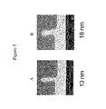
- FIGS. 5A and 5B are SEM images of two alumina mill masks (at about 10 nm and 18 nm thick, respectively) prepared according to one exemplary method.
- FIG. 6 is a contour plot showing critical dimension uniformity of line structures prepared according to an exemplary method.
- FIG. 7 illustrates steps for preparing an ultra-narrow read sensor using an ultra-narrow mill mask according to one exemplary method.
- FIG. 8 is a SEM image of an alumina mill mask remaining above a SiC ultra-narrow line structure prepared as an intermediate step in the exemplary method seen in FIG. 7 .
- FIGS. 9A and 9B are SEM images of two SiC ultra-narrow line structures (at about 10 nm and 18 nm thick, respectively) prepared as an intermediate step in the exemplary method seen in FIG. 7 .
- FIG. 10 is a SEM image of a ultra-narrow reader junction prepared according to the exemplary method seen in FIG. 7 .
- FIG. 11 illustrates steps for preparing an ultra-narrow read sensor using an ultra-narrow mill mask according to another exemplary method.
- FIG. 12 is a SEM image of a ultra-narrow reader junction prepared according to the exemplary method seen in FIG. 11 .
- TW ultra-narrow track width
- the methods utilize side-wall line patterning techniques to prepare ultra-narrow mill masks that can be used to prepare the read sensors.
- the phrase “ultra-narrow” refers to a dimension on the order of less than about 35 nm; such as between about 3 and 35 nm; such as between about 5 and 30 nm; such as between about 5 and 25 nm; such as between about 5 and 20 nm; such as between about 7 and 18 nm; or between about 5 and 10 nm; such as between about 5 and 7 nm; or between about 10 and 18 nm.
- Described herein are side-wall line patterning techniques that are capable of delivering ultra-narrow linewidth structures.
- the side-wall line patterning techniques described herein are capable of delivering well defined linewidths controlled by thickness of a conformally deposited material.
- the conformally deposited material may be applied via an atomic layer deposition technique or the like, which allows for controlled deposition across a wide range of thicknesses as needed for desired reader design and fabrication requirements.
- the conformally deposited material is deposited under such conditions as to provide a high degree of CD uniformity.
- the resulting coated structure can be further processed according to appropriate etching chemistries known in the art to provide an ultra-narrow mill mask on a substrate, which allows for further patterning so as to prepare an ultra-narrow reader junction for use in a read sensor.
- the side-wall line patterning techniques may comprise deposition of one or more sacrificial layers above a substrate, where each sacrificial layer comprises a material that is susceptible to an etching chemistry, such as a reactive ion etching chemistry.
- the one or more sacrificial layers comprises a layer of amorphous carbon.
- the amorphous carbon may be deposited by vapor deposition.
- Various thicknesses of the amorphous carbon layer may be used. In some embodiments, the thickness is less than or equal to about 100 nm thick.
- the one or more sacrificial layers comprises a layer of tantalum. Like amorphous carbon, tantalum may also be deposited by vapor deposition.
- the one or more sacrificial layers may comprise a plurality of sacrificial layers.
- the one or more sacrificial layers comprise a tantalum layer on top of an amorphous carbon layer.
- a masking layer is applied to at least a portion of the uppermost sacrificial layer after the one or more sacrificial layers are in place.
- the masking layer may comprise a material that is not susceptible to the same reactive ion etching chemistry as the uppermost sacrificial layer.
- the masking layer is applied as a photoresist pattern leaving at a portion of the uppermost sacrificial layer exposed. The masking layer may be applied such that an edge of the masking layer defines a straight line along an exposed portion of the uppermost sacrificial layer.
- the initial structure comprises a substrate 1 , two sacrificial layers 2 and 3 , and a masking layer 4 .
- the layered structure is subjected to reactive ion etching chemistries selected to etch the exposed portion of the sacrificial layers.
- the masking layer protects the covered portion of the sacrificial layers, thereby creating a vertical side-wall structure defined by the sacrificial layer materials.
- the masking layer 4 is then removed, exposing a horizontal surface of the uppermost sacrificial layer, and leading to the layered structure seen between steps A and B.
- a SEM image of such an exemplary intermediate layered structure is also seen in FIG. 2 .
- a material capable of conformal deposition is then applied to layered structure, coating the horizontal and vertical surfaces.
- a material capable of “conformal” deposition is a material that is deposited as a coating with substantially even thickness, regardless of the orientation of the surfaces it is being deposited on.
- substantially even thickness means that the variation between surface thickness is less than or equal to about 10%, such as less than or equal to about 5%, such as less than or equal to about 2%, regardless of surface orientation.
- this conformally deposited material is not susceptible to the same reactive ion etching chemistry as at least one of the sacrificial layers.
- the conformally deposited layer 5 applied in step B is the conformally deposited layer 5 applied in step B.
- the conformally deposited material is applied via atomic layer deposition.
- the conformally deposited material comprises alumina (i.e. aluminum oxide).
- alumina i.e. aluminum oxide
- the methods described herein are limited to any particular conformally deposited material being applied by any particular fashion. As described above, it is sufficient that the material is capable of being conformally deposited at a desired thickness, and that the material is not susceptible to the same reactive ion etching chemistry as at least one of the sacrificial layers.
- the deposited material covering a horizontal surface of the uppermost sacrificial layer is removed in a way that leaves at least a portion of the material covering a vertical surface intact. This removal may be accomplished by any method known in the art, including a reactive ion etching specifically targeted to the conformally deposited material. Removal of the conformally deposited material from a horizontal surface of the uppermost sacrificial layer, and subsequent removal of the uppermost sacrificial layer, is seen as step C in FIG. 1 . A SEM image of such an exemplary intermediate structure with a side-wall coating is seen in FIG. 3 .
- the thickness of the side-wall coating is determined by the thickness of the initial conformal deposition.
- atomic layer deposition is particularly useful, as the thickness of the deposited layer can by finely controlled, allowing for deposition of a layer of virtually any desired thickness, such as a thickness less than about 35 nm; such as between about 3 and 35 nm; such as between about 5 and 30 nm; such as between about 5 and 25 nm; such as between about 5 and 20 nm; such as between about 7 and 18 nm; or between about 5 and 10 nm; such as between about 5 and 7 nm; or between about 10 and 18 nm.
- the remaining structure may then be subjected to reactive ion etching specifically directed to remove all remaining sacrificial layer material, leaving a ultra-narrow line structure that can be used to serve as a mill mask for further processing of the underlying substrate.
- This removal step is shown in FIG. 1 as step D, with the resulting ultra-narrow mill mask 6 atop substrate 1 .
- a SEM image of such an exemplary ultra-narrow mill mask atop a substrate is seen in FIG. 4 .
- various embodiments of the methods described herein may be used to provide mill masks with ultra-narrow critical dimension.
- SEM images of two exemplary ultra-narrow mill masks produced by methods described herein are shown in FIG. 5 .
- the thicknesses of the shown ultra-narrow mill masks were measured to be about 10 nm ( FIG. 5A ) and 18 nm ( FIG. 5B ), although thinner mill masks have been produced.
- ultra-narrow mill masks produced by various embodiments presented herein may exhibit high critical dimension uniformity.
- a side-wall patterned mill mask may have a critical dimension uniformity (expressed as within wafer variation) of less than about 1 nm; such as less than about 0.75 nm; such as less than about 0.6 nm.
- An contour plot demonstrating such critical dimension uniformity for a mill mask produced according to one embodiment is seen in FIG. 6 . Observed within wafer variation (WIW sigma) for this example was about 0.58 nm.
- a substrate may be any suitable material or structure.
- a substrate may be a read sensor stack comprising a plurality of layers.
- a side-wall patterned mill mask may be used to further process the substrate to make a read sensor with an ultra-narrow track width.
- a substrate comprises an uppermost layer comprising a material that is susceptible to a reactive ion etching chemistry that is different from any of the one or more sacrificial layers.
- This uppermost layer may be of any suitable thickness, which may be selected based on the chemical identity of the uppermost substrate layer.
- the uppermost substrate layer comprises silicon carbide (SiC). If present as the uppermost substrate layer, silicon carbide may be at any desired thickness, including a thickness of about 50 nm or less.
- the substrate may further comprise an etch stop layer found directly beneath the uppermost substrate layer.
- the etch stop layer comprises a material that is not susceptible to the same reactive ion etching chemistry as the uppermost substrate layer. Again, this uppermost layer may be of any suitable thickness, which may be selected based on the chemical identity of the etch stop layer.
- the etch stop layer may comprise a chromium layer; such as a chromium layer that is about 25 ⁇ thick.
- the initial structure comprises a multi-layered substrate 1 comprising a base layer 7 , an etch stop layer 8 , and an uppermost substrate layer 9 .
- the uppermost substrate layer 9 is subjected to a reactive ion etch so as to remove portions of the substrate layer 9 not protected by the mill mask 6 .
- the resulting line structure is a layered line structure comprising the original mill mask above the protected portion of the substrate layer 9 (shown in FIG. 7 as the structure following step A).
- a SEM image of an exemplary layered line structure prepared according to this method is shown in FIG. 8 .
- the original mill mask may then be removed, leaving a line structure 10 formed of the uppermost substrate material, and with about the same thickness of the original mill mask.
- SEM images of two exemplary line structures are seen in FIGS. 8A (about 10 nm thick) and 8 B (about 18 nm thick).
- the remaining substrate and line structure may then be processed by techniques known in the art to form a reader junction with a track width equal to about the thickness of the line structure 10 .
- a SEM image of an example of a reader junction prepared by this method is seen in FIG. 10 .
- FIG. 11 Another exemplary method for further processing a reader stack substrate into a reader junction is seen in FIG. 11 .
- This exemplary method is simpler than that seen in FIG. 7 in that the side-wall line patterned mill mask 6 is used directly to pattern a reader junction 11 .
- the substrate may comprise a tunneling magnetoresistive (TMR) surface.
- TMR tunneling magnetoresistive
- methods described herein may be used to prepare read sensors comprising a read junction track width of less than about 35 nm; such as between about 3 and 35 nm; such as between about 5 and 30 nm; such as between about 5 and 25 nm; such as between about 5 and 20 nm; such as between about 7 and 18 nm; or between about 5 and 10 nm; such as between about 5 and 7 nm; or between about 10 and 18 nm.
- these read sensors may be used to prepare transducers comprising read sensors with a read junction track width of less than about 35 nm; such as between about 3 and 35 nm; such as between about 5 and 30 nm; such as between about 5 and 25 nm; such as between about 5 and 20 nm; such as between about 7 and 18 nm; or between about 5 and 10 nm; such as between about 5 and 7 nm; or between about 10 and 18 nm.
Abstract
Description
Claims (23)
Priority Applications (2)
| Application Number | Priority Date | Filing Date | Title |
|---|---|---|---|
| US13/929,633 US9406331B1 (en) | 2013-06-17 | 2013-06-27 | Method for making ultra-narrow read sensor and read transducer device resulting therefrom |
| US15/197,503 US20160329064A1 (en) | 2013-06-17 | 2016-06-29 | Method for making ultra-narrow read sensor and read transducer device resulting therefrom |
Applications Claiming Priority (2)
| Application Number | Priority Date | Filing Date | Title |
|---|---|---|---|
| US201361835913P | 2013-06-17 | 2013-06-17 | |
| US13/929,633 US9406331B1 (en) | 2013-06-17 | 2013-06-27 | Method for making ultra-narrow read sensor and read transducer device resulting therefrom |
Related Child Applications (1)
| Application Number | Title | Priority Date | Filing Date |
|---|---|---|---|
| US15/197,503 Continuation US20160329064A1 (en) | 2013-06-17 | 2016-06-29 | Method for making ultra-narrow read sensor and read transducer device resulting therefrom |
Publications (1)
| Publication Number | Publication Date |
|---|---|
| US9406331B1 true US9406331B1 (en) | 2016-08-02 |
Family
ID=56506621
Family Applications (2)
| Application Number | Title | Priority Date | Filing Date |
|---|---|---|---|
| US13/929,633 Expired - Fee Related US9406331B1 (en) | 2013-06-17 | 2013-06-27 | Method for making ultra-narrow read sensor and read transducer device resulting therefrom |
| US15/197,503 Abandoned US20160329064A1 (en) | 2013-06-17 | 2016-06-29 | Method for making ultra-narrow read sensor and read transducer device resulting therefrom |
Family Applications After (1)
| Application Number | Title | Priority Date | Filing Date |
|---|---|---|---|
| US15/197,503 Abandoned US20160329064A1 (en) | 2013-06-17 | 2016-06-29 | Method for making ultra-narrow read sensor and read transducer device resulting therefrom |
Country Status (1)
| Country | Link |
|---|---|
| US (2) | US9406331B1 (en) |
Citations (612)
| Publication number | Priority date | Publication date | Assignee | Title |
|---|---|---|---|---|
| US4502914A (en) | 1982-11-13 | 1985-03-05 | International Business Machines Corporation | Method of making structures with dimensions in the sub-micrometer range |
| US4508579A (en) | 1981-03-30 | 1985-04-02 | International Business Machines Corporation | Lateral device structures using self-aligned fabrication techniques |
| US5199090A (en) | 1992-03-06 | 1993-03-30 | Hewlett-Packard Company | Flying magnetooptical read/write head employing an optical integrated circuit waveguide |
| US5438747A (en) | 1994-03-09 | 1995-08-08 | International Business Machines Corporation | Method of making a thin film merged MR head with aligned pole tips |
| US5612255A (en) | 1993-12-21 | 1997-03-18 | International Business Machines Corporation | One dimensional silicon quantum wire devices and the method of manufacture thereof |
| US5618383A (en) | 1994-03-30 | 1997-04-08 | Texas Instruments Incorporated | Narrow lateral dimensioned microelectronic structures and method of forming the same |
| US5795830A (en) | 1995-06-06 | 1998-08-18 | International Business Machines Corporation | Reducing pitch with continuously adjustable line and space dimensions |
| US5867890A (en) | 1997-12-17 | 1999-02-09 | International Business Machines Corporation | Method for making a thin film merged magnetoresistive read/inductive write head having a pedestal pole tip |
| US5874010A (en) | 1996-07-17 | 1999-02-23 | Headway Technologies, Inc. | Pole trimming technique for high data rate thin film heads |
| US6016290A (en) | 1999-02-12 | 2000-01-18 | Read-Rite Corporation | Read/write head with shifted waveguide |
| US6018441A (en) | 1998-06-08 | 2000-01-25 | Read-Rite Corporation | Disk drive pivot bearing and actuator arm assembly |
| US6025988A (en) | 1998-12-17 | 2000-02-15 | Read-Rite Corporation | Interconnect adapter and head suspension assembly |
| US6025978A (en) | 1996-12-20 | 2000-02-15 | Read-Rite Smi Corporation | Composite type thin-film magnetic head with improved recording characteristics and high resolution |
| US6033532A (en) | 1996-02-27 | 2000-03-07 | Read-Rite Smi Corporation | Oxide film fabrication method and electronic device |
| US6032353A (en) | 1997-05-15 | 2000-03-07 | Read-Rite Corporation | Magnetic head with low stack height and self-aligned pole tips |
| US6034851A (en) | 1998-04-07 | 2000-03-07 | Read-Rite Corporation | Shorting bar and test clip for protecting magnetic heads from damage caused by electrostatic discharge during manufacture |
| US6043959A (en) | 1998-03-23 | 2000-03-28 | Read-Rite Corporation | Inductive write head formed with flat yoke and merged with magnetoresistive read transducer |
| US6043960A (en) | 1997-12-22 | 2000-03-28 | International Business Machines Corporation | Inverted merged MR head with track width defining first pole tip component constructed on a side wall |
| US6046885A (en) | 1998-04-03 | 2000-04-04 | Intri-Plex Technologies, Inc. | Base plate suspension assembly in a hard disk drive with step in flange |
| US6049650A (en) | 1998-04-17 | 2000-04-11 | Seagate Technology, Inc. | Structure for micro-machine optical tooling and method for making and using |
| US6055138A (en) | 1998-05-06 | 2000-04-25 | Read-Rite Corporation | Thin film pedestal pole tips write head having narrower lower pedestal pole tip |
| US6058094A (en) | 1996-07-30 | 2000-05-02 | Seagate Technology Inc. | Flying magneto-optical head with a steerable mirror |
| US6063688A (en) | 1997-09-29 | 2000-05-16 | Intel Corporation | Fabrication of deep submicron structures and quantum wire transistors using hard-mask transistor width definition |
| US6073338A (en) | 1997-08-19 | 2000-06-13 | Read-Rite Corporation | Thin film read head with coplanar pole tips |
| US6078479A (en) | 1993-08-10 | 2000-06-20 | Read-Rite Corporation | Magnetic tape head with flux sensing element |
| US6081499A (en) | 1997-05-05 | 2000-06-27 | Seagate Technology, Inc. | Magneto-optical data storage system having an optical-processing flying head |
| US6094803A (en) | 1999-01-21 | 2000-08-01 | Read-Rite Corporation | Wafer processing techniques for near field magneto-optical head |
| US6099362A (en) | 1996-01-18 | 2000-08-08 | Read-Rite Corporation | Apparatus and method for testing magnetic disk drive components |
| US6103073A (en) | 1996-07-15 | 2000-08-15 | Read-Rite Corporation | Magnetic thin film head zero throat pole tip definition |
| US6108166A (en) | 1998-03-12 | 2000-08-22 | Read-Rite Corporation | Current-pinned spin valve sensor |
| US6118629A (en) | 1997-07-28 | 2000-09-12 | Read-Rite Corporation | Magnetic head with aligned pole tips and pole layers formed of high magnetic moment material |
| US6118638A (en) | 1998-11-02 | 2000-09-12 | Read-Rite Corporation | CPP magnetoresistive device and method for making same |
| US6125018A (en) | 1997-06-10 | 2000-09-26 | Read-Rite Smi Corporation | Composite type thin-film magnetic head |
| US6130779A (en) | 1998-07-06 | 2000-10-10 | Read-Rite Corporation | Near field magneto-optical head made using wafer processing techniques |
| US6134089A (en) | 1999-03-11 | 2000-10-17 | Read-Rite Corporation | Current perpendicular to plane magnetoresistive device with low resistance lead |
| US6137662A (en) | 1998-04-07 | 2000-10-24 | Read-Rite Corporation | Magnetoresistive sensor with pinned SAL |
| US6136166A (en) | 1998-03-27 | 2000-10-24 | Read-Rite Corporation | Apparatus for producing a uniform magnetic field over a large surface area of a wafer |
| US6137661A (en) | 1998-10-19 | 2000-10-24 | Read-Rite Corporation | System for providing a magnetoresistive head having higher efficiency |
| US6160684A (en) | 1998-11-12 | 2000-12-12 | Read-Rite Corporation | Head suspension having tabs and force isolation welds for gram load reduction during swaging |
| US6163426A (en) | 1996-04-23 | 2000-12-19 | Read Rite Corporation | Magnetoresistive head with minimal electromigration |
| US6166891A (en) | 1997-06-30 | 2000-12-26 | Read-Rite Corporation | Magnetoresistive sensor for high temperature environment using iridium manganese |
| US6173486B1 (en) | 1997-03-04 | 2001-01-16 | Read-Rite Corporation | Thin film magnetic head with self-aligned pole tips |
| US6175476B1 (en) | 1998-08-18 | 2001-01-16 | Read-Rite Corporation | Synthetic spin-valve device having high resistivity anti parallel coupling layer |
| US6178066B1 (en) | 1998-05-27 | 2001-01-23 | Read-Rite Corporation | Method of fabricating an improved thin film device having a small element with well defined corners |
| US6178070B1 (en) | 1999-02-11 | 2001-01-23 | Read-Rite Corporation | Magnetic write head and method for making same |
| US6178150B1 (en) | 1996-07-30 | 2001-01-23 | Seagate Technology Inc. | Offset optics for use with optical heads |
| US6181485B1 (en) | 1999-06-23 | 2001-01-30 | Read-Rite Corporation | High numerical aperture optical focusing device for use in data storage systems |
| US6181525B1 (en) | 1998-09-23 | 2001-01-30 | Read-Rite Corporation | Read/write head with a limited range of motion relative to a load beam |
| US6185051B1 (en) | 1999-06-23 | 2001-02-06 | Read-Rite Corporation | High numerical aperture optical focusing device for use in data storage systems |
| US6185081B1 (en) | 1999-06-30 | 2001-02-06 | Read-Rite Corporation | Bias layers which are formed on underlayers promoting in-plane alignment of the c-axis of cobalt used in magnetoresistive transducers |
| US6185077B1 (en) | 1999-01-06 | 2001-02-06 | Read-Rite Corporation | Spin valve sensor with antiferromagnetic and magnetostatically coupled pinning structure |
| US6188549B1 (en) | 1997-12-10 | 2001-02-13 | Read-Rite Corporation | Magnetoresistive read/write head with high-performance gap layers |
| US6190764B1 (en) | 1998-11-23 | 2001-02-20 | Read-Rite Corporation | Inductive write head for magnetic data storage media |
| US6193584B1 (en) | 1999-05-27 | 2001-02-27 | Read-Rite Corporation | Apparatus and method of device stripe height control |
| US6195229B1 (en) | 1998-01-30 | 2001-02-27 | Read-Rite Corporation | Thin film MR head and method of making wherein pole trim takes place at the wafer level |
| US6198608B1 (en) | 1999-03-18 | 2001-03-06 | Read-Rite Corporation | MR sensor with blunt contiguous junction and slow-milling-rate read gap |
| US6198609B1 (en) | 1998-11-09 | 2001-03-06 | Read-Rite Corporation | CPP Magnetoresistive device with reduced edge effect and method for making same |
| US6201673B1 (en) | 1999-04-02 | 2001-03-13 | Read-Rite Corporation | System for biasing a synthetic free layer in a magnetoresistance sensor |
| US6204998B1 (en) | 1996-03-28 | 2001-03-20 | Read-Rite Corporation | Multi-tapped coil having tapped segments cascaded for amplification for improving signal-to-noise ratio |
| US6204999B1 (en) | 1998-12-23 | 2001-03-20 | Read-Rite Corporation | Method and system for providing a write head having a conforming pole structure |
| US6212153B1 (en) | 1998-07-06 | 2001-04-03 | Read-Rite Corporation | High NA solid catadioptric focusing device having a flat kinoform phase profile |
| US6215625B1 (en) | 1999-01-04 | 2001-04-10 | Read-Rite Corporation | Apparatus and method for adhesive bridge suspension attachment |
| US6219205B1 (en) | 1995-10-10 | 2001-04-17 | Read-Rite Corporation | High density giant magnetoresistive transducer with recessed sensor |
| US6222707B1 (en) | 1998-12-28 | 2001-04-24 | Read-Rite Corporation | Bottom or dual spin valve having a seed layer that results in an improved antiferromagnetic layer |
| US6221218B1 (en) | 1998-11-23 | 2001-04-24 | Read-Rite Corporation | Method of forming an inductive write head for magnetic data storage media |
| US6229782B1 (en) | 1998-07-06 | 2001-05-08 | Read-Rite Corporation | High numerical aperture optical focusing device for use in data storage systems |
| US6233116B1 (en) | 1998-11-13 | 2001-05-15 | Read-Rite Corporation | Thin film write head with improved laminated flux carrying structure and method of fabrication |
| US20010001256A1 (en) | 1998-08-24 | 2001-05-17 | Richard Hsiao | Read sensor with self-aligned low resistance leads and method of making |
| US6237215B1 (en) | 1997-02-07 | 2001-05-29 | Read Rite Corporation | Test fixture for positioning and testing a magnetic head |
| US6252743B1 (en) | 1998-11-02 | 2001-06-26 | Read-Rite Corporation | Read/write positioning arm with interspaced amplifier chips |
| US6255721B1 (en) | 1997-08-07 | 2001-07-03 | Read-Rite Corporation | Method and tool for handling micro-mechanical structures |
| US6258468B1 (en) | 1998-12-22 | 2001-07-10 | Read-Rite Corporation | AMR read sensor structure and method with high magnetoresistive coefficient |
| US6266216B1 (en) | 1996-11-08 | 2001-07-24 | Read-Rite Corporation | Inductive/MR composite type thin-film magnetic head with NLTS reduction |
| US6271604B1 (en) | 1999-05-10 | 2001-08-07 | Western Digital Corporation | Integrated computer module having a data integrity latch |
| US6275354B1 (en) | 1998-01-21 | 2001-08-14 | Read-Rite Corporation | Magnetic head with a toroidal coil encompassing only one yoke layer |
| US6277505B1 (en) | 1999-01-21 | 2001-08-21 | Read-Rite Corporation | Read sensor with improved thermal stability and manufacturing method therefor |
| US6282056B1 (en) | 1999-04-08 | 2001-08-28 | Read-Rite Corporation | Tapered stitch pole writer for high density magnetic recording |
| US6291137B1 (en) | 1999-01-20 | 2001-09-18 | Advanced Micro Devices, Inc. | Sidewall formation for sidewall patterning of sub 100 nm structures |
| US6296955B1 (en) | 1999-05-24 | 2001-10-02 | Read-Rite Corporation | High moment and high permeability transducer structures and formation |
| US6297955B1 (en) | 1999-03-31 | 2001-10-02 | Western Digital Ventures, Inc. | Host assembly for an integrated computer module |
| US6304414B1 (en) | 1999-07-20 | 2001-10-16 | Read-Rite Corporation | Thin film magnetic write head having an ultra-low stack height |
| US6307715B1 (en) | 1996-08-30 | 2001-10-23 | Read-Rite Corporation | Head suspension having reduced torsional vibration |
| US6310750B1 (en) | 1999-10-20 | 2001-10-30 | Read-Rite Corporation | Disk drive actuator arm with microactuated read/write head positioning |
| US6310746B1 (en) | 1999-06-23 | 2001-10-30 | Read-Rite Corporation | Piezoelectric vibration damping for disk drives |
| US6317290B1 (en) | 1999-08-31 | 2001-11-13 | Read-Rite Corporation | Advance pole trim writer with moment P1 and low apex angle |
| US6317297B1 (en) | 1999-10-06 | 2001-11-13 | Read-Rite Corporation | Current pinned dual spin valve with synthetic pinned layers |
| US6322911B1 (en) | 1999-02-01 | 2001-11-27 | Read-Rite Corporation | Spin-valve magnetic resistance sensor and thin-film magnetic head |
| US6330137B1 (en) | 1999-06-11 | 2001-12-11 | Read-Rite Corporation | Magnetoresistive read sensor including a carbon barrier layer and method for making same |
| US6330136B1 (en) | 1998-10-14 | 2001-12-11 | Read-Rite Corporation | Magnetic read sensor with SDT tri-layer and method for making same |
| US6333830B2 (en) | 1998-11-09 | 2001-12-25 | Read-Rite Corporation | Low resistance coil structure for high speed writer |
| US6340533B1 (en) | 1998-09-09 | 2002-01-22 | Read-Rite Corporation | Spin-valve magnetoresistance sensor and thin film magnetic head |
| US6349014B1 (en) | 1999-05-14 | 2002-02-19 | Read-Rite Corporation | Magnetic read/write device with insulated coil layer recessed into pole |
| US6351355B1 (en) | 1999-02-09 | 2002-02-26 | Read-Rite Corporation | Spin valve device with improved thermal stability |
| US6353511B1 (en) | 1999-06-15 | 2002-03-05 | Read-Rite Corporation | Thin film write head for improved high speed and high density recording |
| US6353318B1 (en) | 2000-03-10 | 2002-03-05 | Read-Rite Corporation | Magnetoresistive sensor having hard biased current perpendicular to the plane sensor |
| US6356412B1 (en) | 1999-09-30 | 2002-03-12 | Read-Rite Corporation | Air bearing facilitating load/unload of a magnetic read/write head |
| US6359779B1 (en) | 1999-04-05 | 2002-03-19 | Western Digital Ventures, Inc. | Integrated computer module with airflow accelerator |
| US20020034043A1 (en) * | 2000-09-18 | 2002-03-21 | Tomohiro Okada | Single pole type recording head and magnetic storage apparatus |
| US6369983B1 (en) | 1999-08-13 | 2002-04-09 | Read-Rite Corporation | Write head having a dry-etchable antireflective intermediate layer |
| US6377535B1 (en) | 1998-07-06 | 2002-04-23 | Read-Rite Corporation | High numerical aperture optical focusing device having a conical incident facet and a parabolic reflector for use in data storage systems |
| US6376964B1 (en) | 2001-05-16 | 2002-04-23 | Read-Rite Corporation | Collocated rotating flexure microactuator for dual-stage servo in disk drives |
| US6381105B1 (en) | 1999-10-22 | 2002-04-30 | Read-Rite Corporation | Hybrid dual spin valve sensor and method for making same |
| US6381095B1 (en) | 1999-08-31 | 2002-04-30 | Read-Rite Corporation | High performance thin film magnetic write element having high Bsat poles and method for making same |
| US6389499B1 (en) | 1999-06-09 | 2002-05-14 | Western Digital Ventures, Inc. | Integrated computer module |
| US6392850B1 (en) | 1997-04-03 | 2002-05-21 | Read-Rite Corporation | Magnetoresistive transducer having a common magnetic bias using assertive and complementary signals |
| US6396660B1 (en) | 1999-08-23 | 2002-05-28 | Read-Rite Corporation | Magnetic write element having a thermally dissipative structure |
| US6400526B2 (en) | 1999-05-26 | 2002-06-04 | Read-Rite Corporation | Advanced writer for chip-on-load beam |
| US6399179B1 (en) | 1998-04-03 | 2002-06-04 | Intri-Plex Technologies, Inc. | Base plate for suspension assembly in hard disk drive with stress isolation |
| US6404706B1 (en) | 1999-02-12 | 2002-06-11 | Read-Rite Corporation | Laser mounting for a thermally assisted GMR head |
| US6404601B1 (en) | 2000-01-25 | 2002-06-11 | Read-Rite Corporation | Merged write head with magnetically isolated poletip |
| US6410170B1 (en) | 1999-05-20 | 2002-06-25 | Read-Rite Corporation | High resistivity FeXN sputtered films for magnetic storage devices and method of fabrication |
| US6411522B1 (en) | 1999-04-01 | 2002-06-25 | Western Digital Ventures, Inc. | Integrated computer module with EMI shielding plate |
| US6417998B1 (en) | 1999-03-23 | 2002-07-09 | Read-Rite Corporation | Ultra small advanced write transducer and method for making same |
| US6418048B1 (en) | 2001-08-15 | 2002-07-09 | Read-Rite Corporation | Spin-dependent tunneling sensor suitable for a magnetic memory |
| US6417999B1 (en) | 2000-02-04 | 2002-07-09 | Read-Rite Corporation | Magnetoresistive head stabilized structure and method of fabrication thereof |
| US6418000B1 (en) | 1999-01-21 | 2002-07-09 | Read-Rite Corporation | Dual, synthetic spin valve sensor using current pinning |
| US6421212B1 (en) | 1999-09-21 | 2002-07-16 | Read-Rite Corporation | Thin film read head structure with improved bias magnet-to-magnetoresistive element interface and method of fabrication |
| US6424505B1 (en) | 1999-05-06 | 2002-07-23 | Read-Rite Corporation | Method and system for providing electrostatic discharge protection for flex-on suspension, trace-suspension assembly, or cable-on suspension |
| US6423475B1 (en) | 1999-03-11 | 2002-07-23 | Advanced Micro Devices, Inc. | Sidewall formation for sidewall patterning of sub 100 nm structures |
| US6430009B1 (en) | 1999-05-06 | 2002-08-06 | Read-Rite Smi Corporation | Magnetic head shield pole with nonmagnetic separation film between transition portion and shield portion |
| US6433970B1 (en) | 1999-06-07 | 2002-08-13 | Read-Rite Corporation | Structure and method for redeposition free thin film CPP read sensor fabrication |
| US6433965B1 (en) | 2000-03-02 | 2002-08-13 | Read-Rite Corporation | Laminated carbon-containing overcoats for information storage system transducers |
| US6433968B1 (en) | 2000-05-02 | 2002-08-13 | Read-Rite Corporation | Merged read/write head and method of fabricating same |
| US6430806B1 (en) | 2000-06-23 | 2002-08-13 | Read-Rite Corporation | Method for manufacturing an inductive write element employing bi-layer photoresist to define a thin high moment pole pedestal |
| US6437945B1 (en) | 1999-12-28 | 2002-08-20 | Read-Rite Corporation | Airflow assisted ramp loading and unloading of sliders in hard disk drives |
| US6445553B2 (en) | 1999-04-02 | 2002-09-03 | Read-Rite Corporation | Method and system for fabricating a high density magnetoresistive device |
| US6445536B1 (en) | 1998-08-27 | 2002-09-03 | Read-Rite Corporation | Dielectric stencil-defined write head for MR, GMR, and spin valve high density recording heads |
| US6445554B1 (en) | 2000-03-10 | 2002-09-03 | Read-Rite Corporation | Method and system for providing edge-junction TMR for high areal density magnetic recording |
| US6445542B1 (en) | 2000-03-06 | 2002-09-03 | Read-Rite Corporation | Air bearing slider |
| US6447935B1 (en) | 1999-11-23 | 2002-09-10 | Read-Rite Corporation | Method and system for reducing assymetry in a spin valve having a synthetic pinned layer |
| US6448765B1 (en) | 1999-10-28 | 2002-09-10 | Read-Rite Corporation | Microscopic tips having stable magnetic moments and disposed on cantilevers for sensing magnetic characteristics of adjacent structures |
| US6451514B1 (en) | 1998-11-27 | 2002-09-17 | Read-Rite Corporation | Method for formation of upper magnetic pole layer of thin film magnetic head, method of forming miniature block pattern with high aspect ratio on bottom part of step on surface with step, and thin film magnetic head |
| US6452765B1 (en) | 1998-11-18 | 2002-09-17 | Read-Rite Corporation | CoNbTi as high resistivity SAL material for high-density MR |
| US6452742B1 (en) | 1999-09-02 | 2002-09-17 | Read-Rite Corporation | Thin film write having reduced resistance conductor coil partially recessed within middle coat insulation |
| US6456465B1 (en) | 1999-11-09 | 2002-09-24 | Read-Rite Corporation | Vertical giant magnetoresistance sensor using a recessed shield |
| US20020142603A1 (en) | 2001-03-30 | 2002-10-03 | Taiwan Semiconductor Manufacturing Co., Ltd. | Method for forming square-shouldered sidewall spacers and devices fabricated |
| US6462920B1 (en) | 1998-12-23 | 2002-10-08 | Read-Rite Corporation | Method and system for reducing MR head instability |
| US6466401B1 (en) | 1999-06-02 | 2002-10-15 | Read-Rite Corporation | Thin film write head with interlaced coil winding and method of fabrication |
| US6466402B1 (en) | 1999-06-18 | 2002-10-15 | Read-Rite Corporation | Compact MR write structure |
| US6469877B1 (en) | 1999-06-15 | 2002-10-22 | Read-Rite Corporation | Spin valve device with improved exchange layer defined track width and method of fabrication |
| US6472107B1 (en) | 1999-09-30 | 2002-10-29 | Photronics, Inc. | Disposable hard mask for photomask plasma etching |
| US6477019B2 (en) | 1998-10-08 | 2002-11-05 | Read-Rite Smi Corporation | Thin film magnetic head including nonmagnetic and magnetic layers with similar milling rates |
| US6479096B1 (en) | 1999-12-03 | 2002-11-12 | Read-Rite Corporation | Method for manufacturing a GMR spin valve having a smooth interface between magnetic and non-magnetic layers |
| US6483662B1 (en) | 1999-07-09 | 2002-11-19 | Read-Rite Corporation | High density multi-coil magnetic write head having a reduced yoke length and short flux rise time |
| US6490125B1 (en) | 1999-04-09 | 2002-12-03 | Read-Rite Corporation | Thin film write head with improved yoke to pole stitch |
| US6496334B1 (en) | 2000-05-26 | 2002-12-17 | Read-Rite Corportion | Data storage and retrieval apparatus with thin film read head having planarized extra gap and shield layers and method of fabrication thereof |
| US6496330B1 (en) | 1999-09-09 | 2002-12-17 | Read-Rite Corporation | Magnetic write head having a splitcoil structure |
| US6512661B1 (en) | 2000-08-10 | 2003-01-28 | Read-Rite Corporation | Vertical giant magnetoresistance sensor utilizing an insulating bias layer |
| US6512657B2 (en) | 2000-07-17 | 2003-01-28 | Read-Rite Corporation | Head suspension having gram load change reduction and method of assembly |
| US6512690B1 (en) | 2001-08-15 | 2003-01-28 | Read-Rite Corporation | High sensitivity common source amplifier MRAM cell, memory array and read/write scheme |
| US6515573B1 (en) | 2000-06-19 | 2003-02-04 | Read-Rite Corporation | Method and system for providing edge-junction TMR utilizing a hard magnet as a pinned layer |
| US6515791B1 (en) | 2001-04-06 | 2003-02-04 | Read-Rite Corporation | Active reflection and anti-reflection optical switch |
| US6532823B1 (en) | 1999-03-18 | 2003-03-18 | Read-Rite Corporation | Insulator layers for magnetoresistive transducers |
| US6535363B1 (en) | 1999-01-13 | 2003-03-18 | Read-Rite Smi Corporation | Magnetic resistance effect type thin-film magnetic head and method for manufacturing the same |
| US6552928B1 (en) | 2001-02-23 | 2003-04-22 | Read-Rite Corporation | Read-write control circuit for magnetic tunnel junction MRAM |
| US6552874B1 (en) | 2000-05-17 | 2003-04-22 | Read-Rite Corporation | Shared pole magnetic read-write head for achieving optimized erase band width and method of fabricating the same |
| US6566280B1 (en) | 2002-08-26 | 2003-05-20 | Intel Corporation | Forming polymer features on a substrate |
| US6577470B1 (en) | 2001-01-25 | 2003-06-10 | Read-Rite Corporation | Method and system for providing a tape head subassembly structure having an integrated wear bar and outrigger rail |
| US6583968B1 (en) | 2001-10-31 | 2003-06-24 | Western Digital Technologies, Inc. | Spindle motor hub having equivalent MR read element bias voltage to mitigate potential between disk and MR read element |
| US6597548B1 (en) | 1998-06-05 | 2003-07-22 | Read-Rite Smi Corporation | Magnetoresistive element and magnetic head |
| US6611398B1 (en) | 1999-08-09 | 2003-08-26 | Quantum Corporation | Tape head with support bars |
| US6618223B1 (en) | 2000-07-18 | 2003-09-09 | Read-Rite Corporation | High speed, high areal density inductive writer |
| US6629357B1 (en) | 1999-02-10 | 2003-10-07 | Read-Rite Smi Corp. | Method of magnetic head manufacture |
| US6633464B2 (en) | 1998-12-09 | 2003-10-14 | Read-Rite Corporation | Synthetic antiferromagnetic pinned layer with Fe/FeSi/Fe system |
| US6636394B1 (en) | 1999-02-23 | 2003-10-21 | Read-Rite Smi Corp. | Spin-valve magnetic resistance sensor and thin-film magnetic head |
| US6639291B1 (en) | 2002-02-06 | 2003-10-28 | Western Digital (Fremont), Inc. | Spin dependent tunneling barriers doped with magnetic particles |
| US6650506B1 (en) | 1999-12-15 | 2003-11-18 | Patrick Risse | Double-sided disk storage using a single configuration of magnetoresistive head |
| US6654195B1 (en) | 1999-04-27 | 2003-11-25 | Western Digital Ventures, Inc. | Disk drive having a register set for providing real time position variables to a host |
| US6657816B1 (en) | 1999-04-09 | 2003-12-02 | Ronald A. Barr | Thin film inductive read/write head with a sloped pole |
| US6661625B1 (en) | 2001-02-20 | 2003-12-09 | Kyusik Sin | Spin-dependent tunneling sensor with low resistance metal oxide tunnel barrier |
| US6661621B1 (en) | 1999-11-19 | 2003-12-09 | Read-Rite Smi Corp. | Compound thin film magnetic head |
| US6674610B1 (en) | 2000-06-16 | 2004-01-06 | Western Digital (Fremont), Inc. | Thin film write head with universal coil design |
| US6680863B1 (en) | 2002-07-09 | 2004-01-20 | Western Digital (Fremont), Inc. | MRAM memory array having merged word lines |
| US6683763B1 (en) | 2001-08-15 | 2004-01-27 | Western Digital (Fremont), Inc. | Method and system for providing a self-aligned electrical contact for a TMR element |
| US6687098B1 (en) | 1999-07-08 | 2004-02-03 | Western Digital (Fremont), Inc. | Top spin valve with improved seed layer |
| US6687178B1 (en) | 2001-02-23 | 2004-02-03 | Western Digital (Fremont), Inc. | Temperature dependent write current source for magnetic tunnel junction MRAM |
| US6691226B1 (en) | 1999-03-16 | 2004-02-10 | Western Digital Ventures, Inc. | Computer system with disk drive having private key validation means for enabling features |
| US6697294B1 (en) | 2001-02-23 | 2004-02-24 | Western Digital (Fremont), Inc. | Designs of reference cells for magnetic tunnel junction (MTJ) MRAM |
| US6700759B1 (en) | 2000-06-02 | 2004-03-02 | Western Digital (Fremont), Inc. | Narrow track width magnetoresistive sensor and method of making |
| US6700738B1 (en) | 2001-03-16 | 2004-03-02 | Kyusik Sin | Read/write head coil tap having upper and lower portions |
| US6704158B2 (en) | 2001-06-05 | 2004-03-09 | Western Digital (Fremont), Inc. | Shear mode multilayered collocated micro-actuator for dual-stage servo controllers in disk drives |
| US6703312B2 (en) | 2002-05-17 | 2004-03-09 | International Business Machines Corporation | Method of forming active devices of different gatelengths using lithographic printed gate images of same length |
| US6706571B1 (en) | 2002-10-22 | 2004-03-16 | Advanced Micro Devices, Inc. | Method for forming multiple structures in a semiconductor device |
| US6707083B1 (en) | 2002-07-09 | 2004-03-16 | Western Digital (Fremont), Inc. | Magnetic tunneling junction with improved power consumption |
| US6713801B1 (en) | 2002-07-09 | 2004-03-30 | Western Digital (Fremont), Inc. | α-tantalum lead for use with magnetic tunneling junctions |
| US6721149B1 (en) | 2000-02-11 | 2004-04-13 | Western Digital (Fremont), Inc. | Tunneling magnetoresistance spin-valve read sensor with LaNiO3 spacer |
| US6721138B1 (en) | 2001-10-24 | 2004-04-13 | Western Digital (Fremont), Inc. | Inductive transducer with stitched pole tip and pedestal defining zero throat height |
| US6724572B1 (en) | 2002-02-28 | 2004-04-20 | Western Digital, Inc. | Inductive transducer with recessed leading pole layer |
| US6724569B1 (en) | 2000-02-16 | 2004-04-20 | Western Digital (Fremont), Inc. | Thin film writer with multiplayer write gap |
| US6729014B2 (en) | 2001-04-23 | 2004-05-04 | Headway Technologies, Inc. | Magnetic assist read track-width definition for a lead overlay top spin-valve GMR head |
| US6737281B1 (en) | 2002-01-08 | 2004-05-18 | Western Digital (Fremont), Inc. | Method of making transducer with inorganic nonferromagnetic apex region |
| US6744608B1 (en) | 2002-05-14 | 2004-06-01 | Western Digital (Fremont), Inc. | Method and system for making TMR junctions |
| US6747301B1 (en) | 2002-02-06 | 2004-06-08 | Western Digital (Fremont), Inc. | Spin dependent tunneling barriers formed with a magnetic alloy |
| US6751055B1 (en) | 2002-01-08 | 2004-06-15 | Western Digital (Fremont), Inc. | Inductive transducer with reduced pole tip protrusion |
| US6754049B1 (en) | 2001-10-16 | 2004-06-22 | Western Digital (Fremont), Inc. | Transducers for perpendicular recording with inductive cancellation at MR sensor |
| US6757140B1 (en) | 2002-03-19 | 2004-06-29 | Western Digital, Inc. | Electrostatic microelectromechanical (MEM) microactuator for precise read/write head positioning |
| US6760196B1 (en) | 2001-12-12 | 2004-07-06 | Western Digital, Inc. | Microactuator with offsetting hinges and method for high-resolution positioning of magnetic read/write head |
| US6762910B1 (en) | 1999-06-03 | 2004-07-13 | Western Digital (Fremont), Inc. | Data storage and retrieval apparatus with thin film read head having inset extra gap insulation layer and method of fabrication |
| US6765756B1 (en) | 1999-03-12 | 2004-07-20 | Western Digital (Fremont), Inc. | Ultra-short yoke and ultra-low stack height writer and method of fabrication |
| US6778358B1 (en) | 2002-05-01 | 2004-08-17 | Western Digital (Fremont), Inc. | Magnetically soft, high saturation magnetization laminates of iron-cobalt-nitrogen and iron-nickel |
| US6775902B1 (en) | 1997-07-28 | 2004-08-17 | Western Digital (Fremont) Inc. | Method of making a magnetic head with aligned pole tips |
| US6781927B1 (en) | 1996-07-30 | 2004-08-24 | Seagate Technology Llc | Data storage system having an optical processing flying head |
| US6785955B1 (en) | 2001-01-23 | 2004-09-07 | Western Digital (Fremont), Inc. | Method for providing pedestal-defined zero throat writer |
| US6791807B1 (en) | 1998-06-10 | 2004-09-14 | Read-Rite Smi Corporation | Spin-valve magnetic transducing element and magnetic head having free layer with negative magnetostriction |
| US6791793B1 (en) | 2001-09-14 | 2004-09-14 | Western Digital (Fremont), Inc. | Perpendicular recording write head having a recessed magnetic adjunct pole and method of making the same |
| US6798625B1 (en) | 1999-10-28 | 2004-09-28 | Western Digital (Fremont), Inc. | Spin-valve magnetoresistance sensor and thin-film magnetic head |
| US6798616B1 (en) | 2001-07-10 | 2004-09-28 | Western Digital (Fremont), Inc. | Write head architecture for improved manufacturability |
| US6801408B1 (en) | 2000-11-02 | 2004-10-05 | Western Digital (Fremont), Inc. | Data storage and retrieval apparatus with thin film read head having a planar sensor element and an extra gap and method of fabrication thereof |
| US6801411B1 (en) | 1999-02-10 | 2004-10-05 | Western Digital (Fremont), Inc. | Dual stripe spin valve sensor without antiferromagnetic pinning layer |
| US6803615B1 (en) | 2001-02-23 | 2004-10-12 | Western Digital (Fremont), Inc. | Magnetic tunnel junction MRAM with improved stability |
| US6807131B1 (en) | 2000-12-27 | 2004-10-19 | Research Investment Network, Inc. | Near-field hybrid magnetic-optical head system |
| US6806035B1 (en) | 2002-06-25 | 2004-10-19 | Western Digital (Fremont), Inc. | Wafer serialization manufacturing process for read/write heads using photolithography and selective reactive ion etching |
| US6807030B1 (en) | 2001-12-18 | 2004-10-19 | Western Digital (Fremont), Inc. | Enclosed piezoelectric microactuators coupled between head and suspension |
| US6807332B1 (en) | 2000-11-06 | 2004-10-19 | Western Digital (Fremont), Inc. | Piezoelectric actuated optical switch |
| US6809899B1 (en) | 2001-08-20 | 2004-10-26 | Western Digital (Fremont), Inc. | Magnetic heads for perpendicular recording with trapezoidal pole tips |
| US6816345B1 (en) | 2001-09-24 | 2004-11-09 | Western Digital (Fremont), Inc. | Magnetoresistive sensors having submicron track widths and method of making |
| US20040229430A1 (en) | 2003-05-14 | 2004-11-18 | Frank Findeis | Fabrication process for a magnetic tunnel junction device |
| US6829160B1 (en) | 2001-04-06 | 2004-12-07 | Western Digital (Fremont), Inc. | Magnetic ram cell with amplification circuitry and MRAM memory array formed using the MRAM cells |
| US6828897B1 (en) | 1996-08-26 | 2004-12-07 | Western Digital (Fremont), Inc. | Methods and compositions for optimizing interfacial properties of magnetoresistive sensors |
| US6829819B1 (en) | 1999-05-03 | 2004-12-14 | Western Digital (Fremont), Inc. | Method of forming a magnetoresistive device |
| US20050024779A1 (en) | 2003-07-30 | 2005-02-03 | Hitachi Global Storage Technologies, Inc. | Method of making a perpendicular recording magnetic head pole tip with an etchable adhesion CMP stop layer |
| US6859343B1 (en) | 2002-03-19 | 2005-02-22 | Western Digital, Inc. | Hybrid diffuser for minimizing thermal pole tip protrusion and reader sensor temperature |
| US6861937B1 (en) | 2002-06-25 | 2005-03-01 | Western Digital (Fremont), Inc. | Double winding twin coil for thin-film head writer |
| US6861177B2 (en) | 2002-02-21 | 2005-03-01 | Hitachi Global Storage Technologies Netherlands B.V. | Method of forming a read sensor using a lift-off mask having a hardmask layer and a release layer |
| US6859997B1 (en) | 2000-09-19 | 2005-03-01 | Western Digital (Fremont), Inc. | Method for manufacturing a magnetic write element |
| US6862798B2 (en) | 2002-01-18 | 2005-03-08 | Hitachi Global Storage Technologies Netherlands B.V. | Method of making a narrow pole tip by ion beam deposition |
| US6870712B2 (en) | 2001-06-05 | 2005-03-22 | Western Digital (Fremont), Inc. | Inductive writer with flat top pole and pedestal defined zero throat |
| US6873494B2 (en) | 2002-04-29 | 2005-03-29 | Western Digital (Fremont), Inc. | Write head with high moment film layer having tapered portion extending beyond write gap layer |
| US6872467B2 (en) | 2002-11-12 | 2005-03-29 | Nve Corporation | Magnetic field sensor with augmented magnetoresistive sensing layer |
| US6873547B1 (en) | 2001-02-23 | 2005-03-29 | Read Rite Corporation | High capacity MRAM memory array architecture |
| US20050066517A1 (en) | 2003-09-30 | 2005-03-31 | Bedell Daniel Wayne | Ion mill process with sacrificial mask layer to fabricate pole tip for perpendicular recording |
| US6875703B1 (en) | 2004-01-20 | 2005-04-05 | International Business Machines Corporation | Method for forming quadruple density sidewall image transfer (SIT) structures |
| US6879464B2 (en) | 2002-08-16 | 2005-04-12 | Western Digital (Fremont), Inc. | Air bearing having a cavity patch surface coplanar with a leading edge pad surface |
| US6888704B1 (en) | 2003-01-22 | 2005-05-03 | Western Digital (Fremont), Inc. | Method and system for providing high sensitivity giant magnetoresistive sensors |
| US6888184B1 (en) | 2001-02-23 | 2005-05-03 | Western Digital (Fremont), Inc. | Shielded magnetic ram cells |
| US6891702B1 (en) | 2002-10-31 | 2005-05-10 | Western Digital Technologies, Inc. | Method and devices for providing magnetoresistive heads with protection from electrostatic discharge and electric overstress events |
| US6894871B2 (en) | 2002-08-07 | 2005-05-17 | Western Digital (Fremont), Inc. | Technique for reducing pole tip protrusion in a magnetic write head and GMR stripe temperature in an associated read head structure utilizing one or more internal diffuser regions |
| US6893972B2 (en) | 2001-08-31 | 2005-05-17 | Infineon Technologies Ag | Process for sidewall amplification of resist structures and for the production of structures having reduced structure size |
| US20050117251A1 (en) | 2003-11-28 | 2005-06-02 | Tdk Corporation | Thin film magnetic head, method of manufacturing the same, and magnetic recording apparatus |
| US6909578B1 (en) | 2002-05-30 | 2005-06-21 | Western Digital (Fremont), Inc. | Method and system for reducing thermal pole tip protrusion |
| US6912106B1 (en) | 2002-08-06 | 2005-06-28 | Western Digital (Fremont), Inc. | Writer with a hot seed zero throat and substantially flat top pole |
| US6934129B1 (en) | 2002-09-30 | 2005-08-23 | Western Digital (Fremont), Inc. | Magnetoresistive sensor with overlapping lead layers including alpha tantalum and conductive layers |
| US6934113B1 (en) | 2004-03-31 | 2005-08-23 | Western Digital (Fremont), Inc. | Method and system for providing dynamic actuation of a write head using a strain element |
| US20050185332A1 (en) | 2004-02-23 | 2005-08-25 | Hitachi Global Storage Technologies | Perpendicular pole structure and method of fabricating the same |
| US6940688B2 (en) | 2002-10-21 | 2005-09-06 | Western Digital (Fremont), Inc. | Coil inductive writer having a low inductance and short yoke length |
| US6943993B2 (en) | 2003-02-11 | 2005-09-13 | Western Digital (Fremont), Inc. | Magnetic recording head with a side shield structure for controlling side reading of thin film read sensor |
| US6942824B1 (en) | 2002-05-22 | 2005-09-13 | Western Digital (Fremont), Inc. | UV curable and electrically conductive adhesive for bonding magnetic disk drive components |
| US6944938B1 (en) | 1999-05-03 | 2005-09-20 | Western Digital (Fremont), Inc. | Method of forming a magnetoresistive device |
| US6950266B1 (en) | 2002-10-28 | 2005-09-27 | Western Digital (Fremont), Inc. | Active fly height control crown actuator |
| US6958885B1 (en) | 2000-12-21 | 2005-10-25 | Western Digital (Fremont), Inc. | Insulation layer structure for inductive write heads and method of fabrication |
| US6961221B1 (en) | 2001-12-18 | 2005-11-01 | Western Digital (Fremont), Inc. | Piezoelectric microactuators with substantially fixed axis of rotation and magnified stroke |
| US20050241140A1 (en) | 2004-04-30 | 2005-11-03 | Hitachi Global Storage Technologies | High milling resistance write pole fabrication method for perpendicular recording |
| US6969989B1 (en) | 2005-03-11 | 2005-11-29 | Western Digital (Fremont), Inc. | Method for characterizing a perpendicular recording head writing pole |
| US20050264949A1 (en) | 2004-05-28 | 2005-12-01 | Hitachi Global Storage Technologies Netherlands, B.V. | Recessed SiO2 or Si3N4 overcoat for GMR head in magnetic disk drive |
| US6975486B2 (en) | 2002-08-06 | 2005-12-13 | Western Digital (Fremont), Inc. | Thin film write head having a laminated, flat top pole with bottom shaper and method of fabrication |
| US6983531B2 (en) | 2000-12-26 | 2006-01-10 | Headway Technologies, Inc. | Spin valve head having lead overlay |
| US6987643B1 (en) | 2001-10-23 | 2006-01-17 | Western Digital (Fremont), Inc. | Pole structure to relieve adjacent track writing |
| US6989972B1 (en) | 2002-09-30 | 2006-01-24 | Western Digital (Fremont), Inc. | Magnetoresistive sensor with overlapping leads having distributed current |
| US6989962B1 (en) | 2000-09-26 | 2006-01-24 | Western Digital (Fremont), Inc. | Inductive write head having high magnetic moment poles and low magnetic moment thin layer in the back gap, and methods for making |
| US20060028762A1 (en) | 2004-04-30 | 2006-02-09 | Yunxiao Gao | Perpendicular write pole formation using durimide/alumina hard mask without CMP liftoff |
| US7006327B2 (en) | 2003-02-27 | 2006-02-28 | Western Digital (Fremont), Inc. | Thin film recording head with a buried coil providing a shortened yoke and improved dimension control |
| US20060046422A1 (en) | 2004-08-31 | 2006-03-02 | Micron Technology, Inc. | Methods for increasing photo alignment margins |
| US7012832B1 (en) | 2003-10-31 | 2006-03-14 | Western Digital (Fremont), Inc. | Magnetic memory cell with plural read transistors |
| US7015124B1 (en) | 2003-04-28 | 2006-03-21 | Advanced Micro Devices, Inc. | Use of amorphous carbon for gate patterning |
| US20060067001A1 (en) | 2004-09-30 | 2006-03-30 | Yimin Hsu | Thermally assisted recording of magnetic media using a rosonant cavity and energy |
| US7023658B1 (en) | 2000-02-08 | 2006-04-04 | Western Digital (Fremont), Inc. | Submicron track-width pole-tips for electromagnetic transducers |
| US7026063B2 (en) | 2000-04-11 | 2006-04-11 | Western Digital (Fremont), Inc. | Spin-valve type magnetoresistance sensor and thin-film magnetic head |
| US7027268B1 (en) | 1999-07-08 | 2006-04-11 | Western Digital (Fremont), Inc. | Method and system for providing a dual spin filter |
| US7027274B1 (en) | 2001-08-30 | 2006-04-11 | Western Digital (Fremont), Inc. | Spin-dependent tunneling read/write sensor for hard disk drives |
| US7035046B1 (en) | 2002-03-19 | 2006-04-25 | Western Digital (Fremont), Inc. | System and method for minimizing thermal pole tip protrusion |
| US7041985B1 (en) | 2004-11-12 | 2006-05-09 | Western Digital (Fremont), Inc. | Manipulator for microscopy sample preparation and methods for making and use thereof |
| US7046490B1 (en) | 2000-01-06 | 2006-05-16 | Western Digital (Fremont), Inc. | Spin valve magnetoresistance sensor and thin film magnetic head |
| US7054113B1 (en) | 2001-10-25 | 2006-05-30 | Western Digital (Fremont), Inc. | Reader/writer for magnetic memory |
| US7057857B1 (en) | 2002-12-20 | 2006-06-06 | Western Digital (Fremont), Inc. | Dimple pivot post for a rotary co-located microactuator |
| US7059868B1 (en) | 2000-03-07 | 2006-06-13 | Western Digital (Fremont), Inc. | Connection of trace circuitry in a computer disk drive system |
| US7070698B2 (en) | 2004-06-30 | 2006-07-04 | Hitachi Global Storage Technologies Netherlands B.V. | Methods of fabricating magnetic write heads with side and trailing shield structures |
| US20060174474A1 (en) | 2004-04-30 | 2006-08-10 | Hitachi Global Storage Technologies | High milling resistance write pole fabrication method for perpendicular recording |
| US7092195B1 (en) | 2004-05-28 | 2006-08-15 | Western Digital (Fremont), Inc. | Method of using a magnetic write head having an internal heater |
| US7110289B1 (en) | 2004-03-31 | 2006-09-19 | Western Digital (Fremont), Inc. | Method and system for controlling MRAM write current to reduce power consumption |
| US7113366B1 (en) | 2002-11-07 | 2006-09-26 | Western Digital (Fremont), Inc. | Double-nosed inductive transducer with reduced off-track writing |
| US7115525B2 (en) | 2004-09-02 | 2006-10-03 | Micron Technology, Inc. | Method for integrated circuit fabrication using pitch multiplication |
| US7114241B2 (en) | 1998-11-11 | 2006-10-03 | Western Digital (Fremont), Inc. | Method of manufacturing a magnetic head device |
| US7116517B1 (en) | 2002-12-18 | 2006-10-03 | Western Digital (Fremont), Inc. | Stitched pole write element with a T-shaped pole tip portion |
| US7120988B2 (en) | 2003-09-26 | 2006-10-17 | Hitachi Global Storage Technologies Netherlands B.V. | Method for forming a write head having air bearing surface (ABS) |
| US20060234483A1 (en) | 2005-04-19 | 2006-10-19 | Hitachi Global Storage Technologies Netherlands B.V. | CPP read sensor fabrication using heat resistant photomask |
| US7126790B1 (en) | 2003-11-26 | 2006-10-24 | Western Digital (Fremont), Inc. | Magnetic head for perpendicular recording with magnetic loop providing non-perpendicular write field |
| US7124654B1 (en) | 2004-09-30 | 2006-10-24 | Western Digital (Fremont), Inc. | Method for determining a microactuator range of movement |
| US7126788B1 (en) | 2003-11-26 | 2006-10-24 | Western Digital (Fremont), Inc. | Trailing edge recording magnetic head with reversed double bias coil and deflection pole for perpendicular recording with a non-perpendicular write field |
| US7131346B1 (en) | 2004-10-15 | 2006-11-07 | Western Digital (Fremont), Inc. | Spin stand testing system with fine positioner for head stack assembly |
| US7133253B1 (en) | 2002-06-03 | 2006-11-07 | Western Digital (Fremont), Inc. | Pole tip with sides flared at media-facing surface |
| US7133230B2 (en) | 2002-11-05 | 2006-11-07 | Hitachi, Ltd. | Recording head and information recording apparatus |
| US20060273456A1 (en) | 2005-06-02 | 2006-12-07 | Micron Technology, Inc., A Corporation | Multiple spacer steps for pitch multiplication |
| US20060281266A1 (en) | 2005-06-09 | 2006-12-14 | Wells David H | Method and apparatus for adjusting feature size and position |
| US7155732B2 (en) | 2003-09-05 | 2006-12-26 | Seagate Technology Llc | Heat assisted magnetic recording head and method |
| US7170725B1 (en) | 2004-09-01 | 2007-01-30 | Western Digital (Fremont), Inc. | Magnetic sensor having an aluminum-nitride seed layer for an anti-ferromagnetic layer |
| US20070026537A1 (en) | 2005-07-18 | 2007-02-01 | Ming Jiang | Method for fabricating a magnetic head for perpendicular recording using a CMP lift-off and resistant layer |
| US20070026538A1 (en) | 2005-07-29 | 2007-02-01 | Hitachi Global Storage Technologies Netherlands B.V. | Deposition defined trackwidth for very narrow trackwidth CPP device |
| US7186348B2 (en) | 2004-06-30 | 2007-03-06 | Hitachi Global Storage Technologies Netherlands B.V. | Method for fabricating a pole tip in a magnetic transducer |
| US7193815B1 (en) | 2004-04-06 | 2007-03-20 | Western Digital (Fremont), Inc. | Shielded pole magnetic head for perpendicular recording |
| US7196880B1 (en) | 1999-07-19 | 2007-03-27 | Western Digital (Fremont), Inc. | Spin valve sensor having a nonmagnetic enhancement layer adjacent an ultra thin free layer |
| US7199974B1 (en) | 2004-02-02 | 2007-04-03 | Western Digital (Fremont), Inc. | Read/write head with reduced pole tip protrusion |
| US7199975B1 (en) | 2004-05-15 | 2007-04-03 | Western Digital (Fremont), Inc. | Magnetic head for perpendicular recording with hard bias structure for write pole tip |
| US7212384B1 (en) | 2004-02-27 | 2007-05-01 | Western Digital (Fremont), Inc. | Magnetic read head with recessed hard bias and current leads |
| US7211339B1 (en) | 2002-08-22 | 2007-05-01 | Western Digital (Fremont), Inc. | Highly conductive lead adjoining MR stripe and extending beyond stripe height at junction |
| US20070113395A1 (en) | 2005-11-23 | 2007-05-24 | Hitachi Global Storage Technologies | Reference feature design for flare location monitor in perpendicular write pole process |
| US7238292B1 (en) | 2004-07-30 | 2007-07-03 | Western Digital (Fremont), Inc. | Method of fabricating a write element with a reduced yoke length |
| US7239478B1 (en) | 2004-01-31 | 2007-07-03 | Western Digital (Fremont), Inc. | Write element for perpendicular recording in a data storage system |
| US20070159720A1 (en) | 2006-01-10 | 2007-07-12 | Samsung Electronics Co., Ltd. | Heat assisted magnetic recording head and method of manufacturing the same |
| US20070165495A1 (en) | 2006-01-13 | 2007-07-19 | Samsung Electronics Co., Ltd. | Heat assisted magnetic recording head |
| US7248433B1 (en) | 2004-02-02 | 2007-07-24 | Western Digital (Fremont), Inc. | Magnetic head with stitched top pole layer and single layer coil or solenoidal coil |
| US7248431B1 (en) | 2004-04-30 | 2007-07-24 | Yinshi Liu | Method of fabricating a perpendicular recording write head having a gap with two portions |
| US7248449B1 (en) | 2004-03-31 | 2007-07-24 | Western Digital (Fremont), Inc. | Magnetoresistive read sensor with reduced effective shield-to-shield spacing |
| US20070183093A1 (en) | 2006-02-07 | 2007-08-09 | Quang Le | Protective layer for CMP assisted lift-off process and method of fabrication |
| US7280325B1 (en) | 2004-03-31 | 2007-10-09 | Western Digital (Fremont), Llc | Ferromagnetic structure including a first section separated from a ferromagnetic layer by an electrically conductive nonmagnetic spacer and a second section elongated relative to the first section in at least one dimension |
| US7286329B1 (en) | 2003-04-02 | 2007-10-23 | Western Digital (Fremont), Llc | GMR sensor with shallow contiguous junction and bias layers aligned with free sensor layers |
| US7284316B1 (en) | 2004-11-17 | 2007-10-23 | Western Digital (Fremont), Llc | Method for forming a hard bias structure in a magnetoresistive sensor |
| US20070245545A1 (en) | 2006-04-25 | 2007-10-25 | Hitachi Global Storage Technologies | Method of manufacturing a wrap around shield for a perpendicular write pole using a laminated mask |
| US20070245544A1 (en) | 2006-04-25 | 2007-10-25 | Hitachi Global Storage Technologies Netherlands B.V. | Method for making a perpendicular magnetic recording write head |
| US7289303B1 (en) | 2001-04-05 | 2007-10-30 | Western Digital (Fremont), Llc | Spin valve sensors having synthetic antiferromagnet for longitudinal bias |
| US7292409B1 (en) | 2004-02-27 | 2007-11-06 | Western Digital (Fremont), Llc | Magnetic head with thin trailing pedestal layer |
| US7291560B2 (en) | 2005-08-01 | 2007-11-06 | Infineon Technologies Ag | Method of production pitch fractionizations in semiconductor technology |
| US20070258167A1 (en) | 2006-04-25 | 2007-11-08 | Hitachi Global Storage Technologies | Perpendicular magnetic write head having a magnetic write pole with a concave trailing edge |
| US7296339B1 (en) | 2004-09-08 | 2007-11-20 | Western Digital (Fremont), Llc | Method for manufacturing a perpendicular magnetic recording head |
| US7307814B1 (en) | 2002-03-01 | 2007-12-11 | Western Digital (Fremont), Llc | Pedestal defined zero throat writer having a recessed pedestal |
| US7307818B1 (en) | 2004-04-30 | 2007-12-11 | Western Digital (Fremont), Llc | Method and system for providing a stable spin filter |
| US7310204B1 (en) | 2003-12-19 | 2007-12-18 | Western Digital (Fremont), Llc | Inductive writer design for using a soft magnetic pedestal having a high magnetic saturation layer |
| US7318947B1 (en) | 2004-08-31 | 2008-01-15 | Western Digital (Fremont), Llc | Method and apparatus for controlling magnetostriction in a spin valve sensor |
| US7333295B1 (en) | 2004-03-31 | 2008-02-19 | Western Digital (Fremont), Llc | Magnetic recording head with high saturation magnetic flux density CoNiFe thin film composition |
| US7342752B1 (en) | 2004-01-31 | 2008-03-11 | Western Digital (Fremont), Llc | Magnetoresistive read head having a bias structure with at least one dusting layer |
| US7345370B2 (en) | 2005-01-12 | 2008-03-18 | International Business Machines Corporation | Wiring patterns formed by selective metal plating |
| US7349179B1 (en) | 2001-07-16 | 2008-03-25 | Western Digital (Fremont), Llc | Write head for improved manufacturability larger write field and reduced adjacent track erasure |
| US7349170B1 (en) | 2006-04-28 | 2008-03-25 | Western Digital (Fremont), Llc | Method of monitoring operation of a disk drive by analyzing the envelope of a read-back signal in the frequency domain |
| US20080072417A1 (en) | 2006-09-21 | 2008-03-27 | Hitachi Global Storage Technologies | Perpendicular magnetic write pole formation using an aluminum oxide wrap around mask |
| US20080081461A1 (en) | 2006-10-02 | 2008-04-03 | Ji-Young Lee | Method of forming pad patterns using self-align double patterning method, pad pattern layout formed using the same, and method of forming contact holes using self-align double patterning method |
| US7355813B2 (en) | 2002-04-12 | 2008-04-08 | International Business Machines Corporation | Method of fabricating a narrow projection such as a write pole extending from a substrate |
| US20080090418A1 (en) | 2006-10-17 | 2008-04-17 | Jeon Kyung-Yub | Method for forming fine patterns of a semiconductor device using double patterning |
| US7363697B1 (en) | 2005-02-18 | 2008-04-29 | Western Digital (Fremont), Llc | Method for manufacturing a group of head gimbal assemblies |
| US7372665B1 (en) | 2005-01-18 | 2008-05-13 | Western Digital (Fremont), Llc | Magnetic recording head with resistive heating element located near the write coil |
| US7371152B1 (en) | 2006-12-22 | 2008-05-13 | Western Digital (Fremont), Llc | Non-uniform subaperture polishing |
| US7379269B1 (en) | 2004-07-30 | 2008-05-27 | Western Digital (Fremont), Llc | Write element with reduced yoke length for ultra-high density writing |
| US7380332B2 (en) | 2003-06-23 | 2008-06-03 | Hitachi Global Storage Technologies Netherlands B.V. | Magnetic head coil system and damascene/reactive ion etching method for manufacturing the same |
| US7389577B1 (en) | 2007-06-26 | 2008-06-24 | Western Digital (Fremont), Llc | Method to fabricate an ESD resistant tunneling magnetoresistive read transducer |
| US20080149809A1 (en) | 2006-12-26 | 2008-06-26 | Hamann Hendrik F | Method and apparatus for the generation and control of multiple near-field light sources at subwavelength resolution |
| US7417832B1 (en) | 2005-04-26 | 2008-08-26 | Western Digital (Fremont), Llc | Magnetoresistive structure having a novel specular and filter layer combination |
| US7419891B1 (en) | 2006-02-13 | 2008-09-02 | Western Digital (Fremont), Llc | Method and system for providing a smaller critical dimension magnetic element utilizing a single layer mask |
| US7428124B1 (en) | 2005-01-18 | 2008-09-23 | Western Digital (Fremont), Llc | Magnetic recording head with resistive heating element and thermal barrier layer |
| US7430098B1 (en) | 2005-01-18 | 2008-09-30 | Western Digital (Fremont), Llc | Perpendicular magnetic recording head with dynamic flying height heating element |
| US7436620B1 (en) | 2007-05-29 | 2008-10-14 | Western Digital (Fremont), Llc | Method for selecting an electrical power to be applied to a head-based flying height actuator |
| US7440220B1 (en) | 2007-05-29 | 2008-10-21 | Western Digital (Fremont), Llc | Method for defining a touch-down power for head having a flying height actuator |
| US7441325B2 (en) | 2004-04-30 | 2008-10-28 | Hitachi Global Storage Technologies Netherlands B.V. | Perpendicular head with trailing shield and rhodium gap process |
| US7444740B1 (en) | 2005-01-31 | 2008-11-04 | Western Digital (Fremont), Llc | Damascene process for fabricating poles in recording heads |
| US20090017627A1 (en) * | 2007-07-12 | 2009-01-15 | Joseph Neil Greeley | Methods of Modifying Oxide Spacers |
| US7493688B1 (en) | 2006-02-13 | 2009-02-24 | Western Digital (Fremont), Llc | Method of manufacturing a magnetic recording transducer |
| US20090053651A1 (en) | 2007-08-22 | 2009-02-26 | Shin-Etsu Chemical Co., Ltd. | Patterning process |
| US7508627B1 (en) | 2006-03-03 | 2009-03-24 | Western Digital (Fremont), Llc | Method and system for providing perpendicular magnetic recording transducers |
| US20090090418A1 (en) | 2006-12-21 | 2009-04-09 | Parris Earl H | Check valve with fluid hammer relief and monitoring features |
| US7522377B1 (en) | 2002-05-01 | 2009-04-21 | Western Digital (Fremont), Llc | Magnetic write head with high moment magnetic thin film formed over seed layer |
| US7522379B1 (en) | 2004-07-30 | 2009-04-21 | Western Digital (Fremont), Llc | Write element with recessed pole and heat sink layer for ultra-high density writing |
| US7522382B1 (en) | 2005-08-22 | 2009-04-21 | Western Digital (Fremont), Llc | Head stack assembly with interleaved flexure tail bond pad rows |
| US7531456B2 (en) | 2005-12-26 | 2009-05-12 | Samsung Electronics Co., Ltd. | Method of forming self-aligned double pattern |
| US7542246B1 (en) | 2006-04-18 | 2009-06-02 | Western Digital (Fremont), Llc | Transducer with pole tip protrusion compensation layer |
| US7551406B1 (en) | 2005-07-01 | 2009-06-23 | Western Digital (Fremont), Llc | Dual electrical lapping guides with common bonding pad |
| US7552523B1 (en) | 2005-07-01 | 2009-06-30 | Western Digital (Fremont), Llc | Method for manufacturing a perpendicular magnetic recording transducer |
| US7554767B1 (en) | 2005-07-01 | 2009-06-30 | Western Digital (Fremont), Llc | Electrical lapping guide disposed laterally relative to a shield pedestal |
| US7583466B2 (en) | 2007-11-15 | 2009-09-01 | Western Digital (Fremont), Llc | Disk drive determining operating fly height by detecting head disk contact from disk rotation time |
| US7595967B1 (en) | 2004-09-07 | 2009-09-29 | Western Digital (Fremont), Llp | Method for fabricating a spacer layer for a magnetoresistive element |
| US20090266790A1 (en) | 2008-04-28 | 2009-10-29 | Hamid Balamane | Method of making a magnetoresistive reader structure |
| US20090310256A1 (en) | 2008-06-17 | 2009-12-17 | Hitachi Global Storage Technologies Netherlands B.V. | Method for making a master mold with high bit-aspect-ratio for nanoimprinting patterned magnetic recording disks, master mold made by the method, and disk imprinted by the master mold |
| US7639457B1 (en) | 2004-02-27 | 2009-12-29 | Western Digital (Fremont), Llc | Magnetic sensor with underlayers promoting high-coercivity, in-plane bias layers |
| US20100024201A1 (en) | 2008-07-31 | 2010-02-04 | Quang Le | Method for fabricating narrow magnetic read width tmr/cpp sensors |
| US7660080B1 (en) | 2004-04-30 | 2010-02-09 | Western Digital (Fremont), Llc | Read/write head with dynamic flying height control by magnetostriction |
| US7666578B2 (en) | 2006-09-14 | 2010-02-23 | Micron Technology, Inc. | Efficient pitch multiplication process |
| US7672086B1 (en) | 2004-04-28 | 2010-03-02 | Western Digital (Fremont), Llc | Method and system for providing a magnetic element having a current confined layer |
| US7672080B1 (en) | 2006-09-15 | 2010-03-02 | Western Digital (Fremont), Llc | Laminated perpendicular writer head including amorphous metal |
| US7684160B1 (en) | 2006-02-06 | 2010-03-23 | Western Digital (Fremont), Llc | Magnetoresistive structure having a novel specular and barrier layer combination |
| US7688546B1 (en) | 2006-12-21 | 2010-03-30 | Western Digital (Fremont), Llc | Perpendicular magnetic recording head having nonmagnetic insertion layers |
| US7695761B1 (en) | 2006-12-21 | 2010-04-13 | Western Digital (Fremont), Llc | Method and system for providing a spin tunneling magnetic element having a crystalline barrier layer |
| US7719795B2 (en) | 2006-11-15 | 2010-05-18 | Western Digital (Fremont), Llc | Head having a transducer heater and an air bearing surface with a flow-diversion dam and pressure-relief trough disposed upstream of the transducer |
| US7736823B1 (en) | 2007-05-11 | 2010-06-15 | Western Digital (Fremont), Llc | Method and system for providing optical proximity correction for structures such as a PMR nose |
| US7785666B1 (en) | 2007-12-12 | 2010-08-31 | Western Digital (Fremont), Llc | Methods for fabricating a magnetic recording device |
| US7796356B1 (en) | 2009-05-04 | 2010-09-14 | Western Digital (Fremont), Llc | Head integrated touchdown sensor for hard disk drives |
| US7800858B1 (en) | 2009-05-04 | 2010-09-21 | Western Digital (Fremont), Llc | Differential head integrated touchdown sensors for hard disk drives |
| US7819979B1 (en) | 2005-01-31 | 2010-10-26 | Western Digital (Fremont), Llc | Method and system for cleaning magnetic artifacts using a carbonyl reactive ion etch |
| US7829264B1 (en) | 2007-08-09 | 2010-11-09 | Western Digital (Fremont), Llc | Method and system for providing a microelectronic device using a plurality of focus distances |
| US20100290157A1 (en) | 2009-05-14 | 2010-11-18 | Western Digital (Fremont), Llc | Damascene coil processes and structures |
| US7846643B1 (en) | 2007-11-02 | 2010-12-07 | Western Digital (Fremont), Llc | Method and system for providing a structure in a microelectronic device using a chromeless alternating phase shift mask |
| US7855854B2 (en) | 2007-04-17 | 2010-12-21 | Western Digital (Fremont), Llc | Head with an air bearing surface having a shallow recessed trailing air flow dam |
| US7869160B1 (en) | 2005-04-27 | 2011-01-11 | Western Digital (Fremont), Llc | Perpendicular recording head with shaped pole surfaces for higher linear data densities |
| US7872824B1 (en) | 2007-06-11 | 2011-01-18 | Western Digital (Fremont), Llc | Setting an operating bias current for a magnetoresistive head by computing a target operating voltage |
| US7872833B2 (en) | 2007-04-17 | 2011-01-18 | Western Digital (Fremont) , LLC | Head with a transducer overcoat having a trailing air flow dam that is shallowly recessed from an air bearing surface |
| US7910267B1 (en) | 2008-12-12 | 2011-03-22 | Western Digital (Fremont), Llc | Method and system for providing optical proximity correction for structures such as a PMR nose |
| US7911735B1 (en) | 2007-03-09 | 2011-03-22 | Western Digital (Fremont), Llc | Perpendicular magnetic recording head utilizing a nonmagnetic underlayer layer |
| US7911737B1 (en) | 2007-03-23 | 2011-03-22 | Western Digital (Fremont), Llc | Method and system for providing a PMR head having an antiferromagnetically coupled pole |
| US7916426B2 (en) | 2007-11-30 | 2011-03-29 | Western Digital (Fremont), Llc | Head with an air bearing surface having left and right leading pressurizing steps, each with short and long regions |
| US20110086240A1 (en) | 2009-10-14 | 2011-04-14 | Western Digital (Fremont), Llc | Double patterning hard mask for damascene perpendicular magnetic recording (pmr) writer |
| US7982989B1 (en) | 2009-12-23 | 2011-07-19 | Western Digital (Fremont), Llc | Method and system for measuring magnetic interference width |
| US8008912B1 (en) | 2008-12-16 | 2011-08-30 | Western Digital (Fremont), Llc | Method and system for testing P2 stiffness of a magnetoresistance transducer at the wafer level |
| US8012804B1 (en) | 2009-12-23 | 2011-09-06 | Western Digital (Fremont), Llc | Method and system for mounting lasers on energy assisted magnetic recording heads |
| US8015692B1 (en) | 2007-11-07 | 2011-09-13 | Western Digital (Fremont), Llc | Method for providing a perpendicular magnetic recording (PMR) head |
| US8018678B1 (en) | 2008-11-26 | 2011-09-13 | Western Digital (Fremont), Llc | Method for simultaneous electronic lapping guide (ELG) and perpendicular magnetic recording (PMR) pole formation |
| US8024748B1 (en) | 2009-09-09 | 2011-09-20 | Western Digital Technologies, Inc. | Method and system for coupling a laser with a slider in an energy assisted magnetic recording disk drive |
| US8072705B1 (en) | 2007-05-11 | 2011-12-06 | Western Digital (Fremont), Llc | Method and system for providing a magnetic writer using a BARC |
| US8077557B1 (en) | 2009-05-19 | 2011-12-13 | Western Digital (Fremont), Llc | Multiple aperture VCSEL EAMR heads |
| US8074345B1 (en) | 2009-05-18 | 2011-12-13 | Western Digital (Fremont), Llc | Method of measuring a bevel angle in a write head |
| US8077434B1 (en) | 2007-11-19 | 2011-12-13 | Western Digital (Fremont), Llc | Perpendicular magnetic recording head having a recessed magnetic base layer |
| US8077418B1 (en) | 2009-03-31 | 2011-12-13 | Western Digital (Fremont), Llc | Reducing thermal protrusion of a near field transducer in an energy assisted magnetic recording head |
| US8077435B1 (en) | 2008-11-20 | 2011-12-13 | Western Digital (Fremont), Llc | Current perpendicular-to-plane read sensor with back shield |
| US8079135B1 (en) | 2007-12-13 | 2011-12-20 | Western Digital (Fremont), Llc | Method for providing a perpendicular magnetic recording (PMR) transducer |
| US8091210B1 (en) | 2008-03-05 | 2012-01-10 | Western Digital (Fremont), Llc | Method for providing a structure in magnetic recording transducer |
| US8097846B1 (en) | 2009-02-25 | 2012-01-17 | Western Digital (Fremont), Llc | Metrology and 3D reconstruction of devices in a wafer |
| US8104166B1 (en) | 2003-12-19 | 2012-01-31 | Western Digital (Fremont), Llc | Self-aligned method for fabricating a high density GMR read element |
| US8116171B1 (en) | 2009-11-11 | 2012-02-14 | Western Digital (Fremont), Llc | Method and system for providing energy assisted magnetic recording disk drive using a vertical surface emitting laser |
| US8116043B2 (en) | 2009-12-09 | 2012-02-14 | Western Digital (Fremont), Llc | Method and system for providing a magnetic transducer having an improved read sensor synthetic antiferromagnet |
| US8125856B1 (en) | 2009-11-05 | 2012-02-28 | Western Digital (Fremont), Llc | Method and system for optically coupling a laser with a transducer in an energy assisted magnetic recording disk drive |
| US8134794B1 (en) | 2009-12-23 | 2012-03-13 | Western Digital (Fremont), Llc | Method and system for providing an energy assisted magnetic recording head in a wafer packaging configuration |
| US8136805B1 (en) | 2008-11-19 | 2012-03-20 | Western Digital (Fremont), Llc | Row bar holder |
| US8136224B1 (en) | 2008-05-15 | 2012-03-20 | Western Digital (Fremont), Llc | Method and system for providing a perpendicular magnetic recording head utilizing a mask having an undercut line |
| US8136225B1 (en) | 2008-05-15 | 2012-03-20 | Western Digital (Fremont), Llc | Method and system for providing a perpendicular magnetic recording head |
| US8141235B1 (en) | 2006-06-09 | 2012-03-27 | Western Digital (Fremont), Llc | Method for manufacturing a perpendicular magnetic recording transducers |
| US8146236B1 (en) | 2008-03-28 | 2012-04-03 | Western Digital (Fremont), Llc | Method for providing a perpendicular magnetic recording (PMR) transducer |
| US8151441B1 (en) | 2008-03-27 | 2012-04-10 | Western Digital (Fremont), Llc | Method for providing and utilizing an electronic lapping guide in a magnetic recording transducer |
| US8164855B1 (en) | 2009-11-06 | 2012-04-24 | Western Digital (Fremont), Llc | Method and system for providing a write pole in an energy assisted magnetic recording disk drive |
| US8165709B1 (en) | 2009-02-26 | 2012-04-24 | Western Digital (Fremont), Llc | Four pad self-calibrating electronic lapping guide |
| US8163185B1 (en) | 2008-03-31 | 2012-04-24 | Western Digital (Fremont), Llc | Method and apparatus for lifting off photoresist beneath an overlayer |
| US8164864B2 (en) | 2009-07-16 | 2012-04-24 | Western Digital (Fremont), Llc | Method and system for fabricating magnetic transducers with improved pinning |
| US8164760B2 (en) | 2010-03-11 | 2012-04-24 | Western Digital (Fremont), Llc | Method and system for interrogating the thickness of a carbon layer |
| US8169473B1 (en) | 2008-03-27 | 2012-05-01 | Western Digital (Fremont), Llc | Method and system for exposing a photoresist in a magnetic device |
| US8166632B1 (en) | 2008-03-28 | 2012-05-01 | Western Digital (Fremont), Llc | Method for providing a perpendicular magnetic recording (PMR) transducer |
| US8166631B1 (en) | 2008-08-27 | 2012-05-01 | Western Digital (Fremont), Llc | Method for fabricating a magnetic recording transducer having side shields |
| US8171618B1 (en) | 2009-06-17 | 2012-05-08 | Western Digital (Fremont), Llc | Tunable pole trim processes for fabricating trapezoidal perpendicular magnetic recording (PMR) write poles |
| US20120111826A1 (en) | 2010-11-10 | 2012-05-10 | Western Digital (Fremont), Llc | Damascene process using pvd sputter carbon film as cmp stop layer for forming a magnetic recording head |
| US8179636B1 (en) | 2008-03-05 | 2012-05-15 | Western Digital (Fremont), Llc | Method and system for providing a perpendicular magnetic recording writer |
| US20120129349A1 (en) * | 2010-11-23 | 2012-05-24 | Yun-Seung Kang | Method of forming patterns for semiconductor device |
| US8194365B1 (en) | 2009-09-03 | 2012-06-05 | Western Digital (Fremont), Llc | Method and system for providing a read sensor having a low magnetostriction free layer |
| US8194366B1 (en) | 2009-10-14 | 2012-06-05 | Western Digital (Fremont), Llc | TMR read head structures with differential stripe heights |
| US8191237B1 (en) | 2009-05-21 | 2012-06-05 | Western Digital (Fremont), Llc | Method for providing a structure in a magnetic transducer |
| US8196285B1 (en) | 2008-12-17 | 2012-06-12 | Western Digital (Fremont), Llc | Method and system for providing a pole for a perpendicular magnetic recording head using a multi-layer hard mask |
| US8200054B1 (en) | 2009-04-19 | 2012-06-12 | Western Digital (Fremont), Llc | High efficiency grating coupling for light delivery in EAMR |
| US8203800B2 (en) | 2009-03-05 | 2012-06-19 | Western Digital (Fremont), Llc | Servo design in data storage media |
| US8222599B1 (en) | 2009-04-15 | 2012-07-17 | Western Digital (Fremont), Llc | Precise metrology with adaptive milling |
| US8220140B1 (en) | 2010-09-13 | 2012-07-17 | Western Digital (Fremont), Llc | System for performing bonding a first substrate to a second substrate |
| US8225488B1 (en) | 2009-05-22 | 2012-07-24 | Western Digital (Fremont), Llc | Method for providing a perpendicular magnetic recording (PMR) pole |
| US8227023B1 (en) | 2009-05-27 | 2012-07-24 | Western Digital (Fremont), Llc | Method and system for fabricating magnetic transducers with improved pinning |
| US8228633B1 (en) | 2008-08-21 | 2012-07-24 | Western Digital (Fremont), Llc | Method and system for providing a magnetic recording transducer having a hybrid moment pole |
| US8231796B1 (en) | 2008-12-09 | 2012-07-31 | Western Digital (Fremont), Llc | Method and system for providing a magnetic recording transducer having side shields |
| US8233248B1 (en) | 2009-09-16 | 2012-07-31 | Western Digital (Fremont), Llc | Method and system for providing a magnetic recording transducer using a line hard mask |
| US8248896B1 (en) | 2010-06-24 | 2012-08-21 | Western Digital (Fremont), Llc | Method and system for providing an energy assisted magnetic recording disk drive having improved heat dissipation |
| US8254060B1 (en) | 2009-04-17 | 2012-08-28 | Western Digital (Fremont), Llc | Straight top main pole for PMR bevel writer |
| US20120216378A1 (en) | 2010-03-24 | 2012-08-30 | Wester Digital (Fremont), Llc | Method and system for providing a piezoelectric multilayer |
| US8259410B1 (en) | 2008-05-23 | 2012-09-04 | Western Digital (Fremont), Llc | Method and system for providing a magnetic head using a composite magnetic material in the recording transducer |
| US8257597B1 (en) | 2010-03-03 | 2012-09-04 | Western Digital (Fremont), Llc | Double rie damascene process for nose length control |
| US8259539B1 (en) | 2008-12-17 | 2012-09-04 | Western Digital (Fremont), Llc | Integration of a vertical cavity surface emitting laser (VCSEL) on an energy-assisted magnetic recording (EAMR) head |
| US8264798B1 (en) | 2010-06-23 | 2012-09-11 | Western Digital (Fremont), Llc | Systems and methods for providing magnetic recording heads adapted for writing shingled tracks |
| US8264797B2 (en) | 2009-12-21 | 2012-09-11 | Western Digital (Fremont), Llc | Head gimbal assembly having a radial rotary piezoelectric microactuator between a read head and a flexure tongue |
| US8262918B1 (en) | 2009-03-25 | 2012-09-11 | Western Digital (Fremont), Llc | Methods of producing damascene main pole for perpendicular magnetic recording head |
| US8262919B1 (en) | 2010-06-25 | 2012-09-11 | Western Digital (Fremont), Llc | Method and system for providing a perpendicular magnetic recording pole using multiple chemical mechanical planarizations |
| US8270126B1 (en) | 2008-06-16 | 2012-09-18 | Western Digital (Fremont), Llc | Method and system for providing an improved hard bias structure |
| US20120237878A1 (en) | 2011-03-18 | 2012-09-20 | Western Digital (Fremont), Llc | Method and system for providing a side shield for a perpendicular magnetic recording pole |
| US8276258B1 (en) | 2008-08-26 | 2012-10-02 | Western Digital (Fremont), Llc | Method for fabricating a magnetic recording transducer |
| US8277669B1 (en) | 2009-12-21 | 2012-10-02 | Western Digital (Fremont), Llc | Method and system for providing a perpendicular magnetic recording pole having a leading edge bevel |
| US8279719B1 (en) | 2009-10-01 | 2012-10-02 | Western Digital (Fremont), Llc | Method and system for coupling a laser with a slider in an energy assisted magnetic recording disk drive |
| US8288204B1 (en) | 2011-08-30 | 2012-10-16 | Western Digital (Fremont), Llc | Methods for fabricating components with precise dimension control |
| US8289821B1 (en) | 2010-12-21 | 2012-10-16 | Western Digital (Fremont), Llc | Method and system for pulsing EAMR disk drives |
| US8291743B1 (en) | 2009-05-27 | 2012-10-23 | Western Digital (Fremont), Llc | Method and system for calibrating an electronic lapping guide for a beveled pole in a magnetic recording transducer |
| US8307540B1 (en) | 2011-03-10 | 2012-11-13 | Western Digital (Fremont), Llc | Method for providing an energy assisted magnetic recording (EAMR) transducer |
| US8308921B1 (en) | 2006-12-21 | 2012-11-13 | Western Digital (Fremont), Llc | Mask for increased uniformity in ion beam deposition |
| US8307539B1 (en) | 2009-09-30 | 2012-11-13 | Western Digital (Fremont), Llc | Method for modeling devices in a wafer |
| US8310901B1 (en) | 2010-06-09 | 2012-11-13 | Western Digital (Fremont), Llc | Method and system for providing separate write and optical modules in an energy assisted magnetic recording disk drive |
| US8315019B1 (en) | 2009-03-31 | 2012-11-20 | Western Digital (Fremont), Llc | Method and system for providing an improved magnetoresistive structure utilizing an oxidation buffer layer |
| US8320722B1 (en) | 2010-04-13 | 2012-11-27 | Western Digital (Fremont), Llc | Non-linear optical grating |
| US8316527B2 (en) | 2008-04-01 | 2012-11-27 | Western Digital (Fremont), Llc | Method for providing at least one magnetoresistive device |
| US8320077B1 (en) | 2008-12-15 | 2012-11-27 | Western Digital (Fremont), Llc | Method and system for providing a high moment film |
| US8320220B1 (en) | 2011-10-13 | 2012-11-27 | Western Digital (Fremont), Llc | Method and system for providing an energy assisted magnetic recording disk drive having a non-conformal heat spreader |
| US8320076B1 (en) | 2008-06-26 | 2012-11-27 | Western Digital (Fremont), Llc | Method and system for providing a magnetic recording transducer including an assist pole having surfaces angled with respect to the ABS |
| US8320219B1 (en) | 2010-06-15 | 2012-11-27 | Western Digital (Fremont), Llc | Trailing edge optimized near field transducer |
| US20120298621A1 (en) | 2011-05-25 | 2012-11-29 | Western Digital (Fremont), Llc | Method and system for fabricating a narrow line structure in a magnetic recording head |
| US8322022B1 (en) | 2010-06-28 | 2012-12-04 | Western Digital (Fremont), Llc | Method for providing an energy assisted magnetic recording head in a wafer packaging configuration |
| US8325569B1 (en) | 2011-06-27 | 2012-12-04 | Western Digital (Fremont), Llc | EAMR head having improved optical coupling efficiency |
| US8322023B1 (en) | 2009-11-10 | 2012-12-04 | Western Digital (Fremont), Llc | Method for providing a wrap-around shield for a magnetic recording transducer |
| US8333008B1 (en) | 2005-07-29 | 2012-12-18 | Western Digital (Fremont), Llc | Method for manufacturing a perpendicular magnetic recording transducer |
| US8334093B2 (en) | 2008-10-31 | 2012-12-18 | Western Digital (Fremont), Llc | Method and system for providing a perpendicular magnetic recording head |
| US8333898B2 (en) | 2010-12-20 | 2012-12-18 | Hitachi Global Storage Technologies Netherlands B.V. | Method for manufacturing a magnetic tape head using a TMR sensor |
| US8336194B2 (en) | 2009-11-03 | 2012-12-25 | Western Digital (Fremont), Llc | Method of fabricating a tunneling magnetoresistive (TMR) reader |
| US8343319B1 (en) | 2008-09-25 | 2013-01-01 | Western Digital (Fremont), Llc | Method and system for providing an improved hard bias structure |
| US8341826B1 (en) | 2010-04-12 | 2013-01-01 | Western Digital (Fremont), Llc | Method for fabricating a magnetic recording transducer using a split seed layer |
| US8343364B1 (en) | 2010-06-08 | 2013-01-01 | Western Digital (Fremont), Llc | Double hard-mask mill back method of fabricating a near field transducer for energy assisted magnetic recording |
| US20130005113A1 (en) * | 2011-06-30 | 2013-01-03 | Elpida Memory, Inc. | Method of manufacturing semiconductor device |
| US8349195B1 (en) | 2008-06-27 | 2013-01-08 | Western Digital (Fremont), Llc | Method and system for providing a magnetoresistive structure using undercut free mask |
| US8351307B1 (en) | 2010-06-04 | 2013-01-08 | Western Digital (Fremont), Llc | Trailing edge optimized near field transducer having non-rectangular pin cross section |
| US8357244B1 (en) | 2007-06-28 | 2013-01-22 | Western Digital (Fremont), Llc | Method for lifting off photoresist beneath an overlayer |
| US8373945B1 (en) | 2007-04-23 | 2013-02-12 | Western Digital (Fremont), Llc | Magnetic writer having a split yoke |
| US8375564B1 (en) | 2009-12-08 | 2013-02-19 | Western Digital (Fremont), Llc | Method for fabricating a pole of a magnetic transducer |
| US8375565B2 (en) | 2010-05-28 | 2013-02-19 | Western Digital (Fremont), Llc | Method for providing an electronic lapping guide corresponding to a near-field transducer of an energy assisted magnetic recording transducer |
| US8381391B2 (en) | 2009-06-26 | 2013-02-26 | Western Digital (Fremont), Llc | Method for providing a magnetic recording transducer |
| US8385158B1 (en) | 2009-10-06 | 2013-02-26 | Western Digital (Fremont), Llc | Method and system for providing a magnetic recording transducer having a planarized near-field transducer and a sloped pole |
| US8385157B1 (en) | 2009-09-30 | 2013-02-26 | Western Digital Technologies, Inc. | Method and system for performing EAMR recording at high density using a large thermal spot size |
| US8394280B1 (en) | 2009-11-06 | 2013-03-12 | Western Digital (Fremont), Llc | Resist pattern protection technique for double patterning application |
| US8400731B1 (en) | 2009-04-19 | 2013-03-19 | Western Digital (Fremont), Llc | Write head with variable side shield gaps |
| US8405930B1 (en) | 2011-03-23 | 2013-03-26 | Western Digital (Fremont), Llc | Method and system for providing a transducer having dual, ABS recessed auxiliary poles on opposite sides of a main pole with non-magnetic spacer adjoining back portion of main pole and positioned between auxiliary poles |
| US8404129B1 (en) | 2010-03-31 | 2013-03-26 | Western Digital (Fremont), Llc | Method and system for providing a curved surface in a magnetic recording head |
| US8404128B1 (en) | 2009-02-23 | 2013-03-26 | Western Digital (Fremont), Llc | Method and system for providing a perpendicular magnetic recording head |
| US8409453B1 (en) | 2010-05-12 | 2013-04-02 | Western Digital (Fremont), Llc | Method and system for providing a wrap-around shield using a patterned seed layer |
| US8413317B1 (en) | 2010-11-12 | 2013-04-09 | Western Digital (Fremont), Llc | Method for fabricating a structure for a microelectric device |
| US8416540B1 (en) | 2008-06-26 | 2013-04-09 | Western Digital (Fremont), Llc | Method for defining a magnetoresistive junction using multiple mills at a plurality of angles |
| US8422342B1 (en) | 2010-06-25 | 2013-04-16 | Western Digital (Fremont), Llc | Energy assisted magnetic recording disk drive using a distributed feedback laser |
| US8419953B1 (en) | 2011-06-28 | 2013-04-16 | Western Digital (Fremont), Llc | Method and system for removing an antiferromagnetic seed structure |
| US8419954B1 (en) | 2011-10-31 | 2013-04-16 | Western Digital (Fremont), Llc | Method for providing a side shield for a magnetic recording transducer |
| US8422841B1 (en) | 2010-05-13 | 2013-04-16 | Western Digital (Fremont), Llc | Double optical grating |
| US8422176B1 (en) | 2011-11-15 | 2013-04-16 | Western Digital (Fremont), Llc | Method and system for providing a magnetic read transducer having a bilayer magnetic seed layer |
| US8424192B1 (en) | 2005-08-08 | 2013-04-23 | Western Digital (Fremont), Llc | Method for manufacturing a pole for a magnetic recording head |
| US8441756B1 (en) | 2010-12-16 | 2013-05-14 | Western Digital (Fremont), Llc | Method and system for providing an antiferromagnetically coupled writer |
| US8443510B1 (en) | 2009-05-28 | 2013-05-21 | Western Digital (Fremont), Llc | Method for utilizing an electronic lapping guide for a beveled pole in a magnetic recording transducer |
| US8444866B1 (en) | 2010-09-21 | 2013-05-21 | Westen Digital (Fremont), LLC | Method and system for providing a perpendicular magnetic recording pole with a multi-layer side gap |
| US8449948B2 (en) | 2009-09-10 | 2013-05-28 | Western Digital (Fremont), Llc | Method and system for corrosion protection of layers in a structure of a magnetic recording transducer |
| US8451556B1 (en) | 2009-12-23 | 2013-05-28 | Western Digital (Fremont), Llc | Method and system for providing a molded capping layer for an energy assisted magnetic recording head |
| US8451563B1 (en) | 2011-12-20 | 2013-05-28 | Western Digital (Fremont), Llc | Method for providing a side shield for a magnetic recording transducer using an air bridge |
| US8456961B1 (en) | 2011-03-22 | 2013-06-04 | Western Digital (Fremont), Llc | Systems and methods for mounting and aligning a laser in an electrically assisted magnetic recording assembly |
| US8456967B1 (en) | 2011-10-12 | 2013-06-04 | Western Digital (Fremont), Llc | Systems and methods for providing a pole pedestal for microwave assisted magnetic recording |
| US8456964B1 (en) | 2010-11-16 | 2013-06-04 | Western Digital (Fremont), Llc | Energy assisted magnetic recording head having a reflector for improving efficiency of the light beam |
| US8456963B1 (en) | 2010-04-12 | 2013-06-04 | Western Digital (Fremont), Llc | Method and system for an energy assisted magnetic recording head having a suspension-mounted laser |
| US8456966B1 (en) | 2010-12-17 | 2013-06-04 | Western Digital (Fremont), Llc | Method and system for enhancing optical efficiency for an EAMR head |
| US8454846B1 (en) | 2010-06-17 | 2013-06-04 | Western Digital (Fremont), Llc | Method and system for providing a full wrap-around shield using a frame configured wet etch in a damascene process |
| US8458892B2 (en) | 2010-05-11 | 2013-06-11 | Western Digital (Fremont), Llc | Method for providing a perpendicular magnetic recording transducer using a low energy mill |
| US8462592B1 (en) | 2010-11-17 | 2013-06-11 | Western Digital (Fremont), Llc | Energy-assisted magnetic recording head having waveguide capable of providing small beam spots |
| US8480911B1 (en) | 2011-06-30 | 2013-07-09 | Western Digital (Fremont), Llc | Method and system for providing a read sensor in a magnetic recording transducer using focused ion beam scan polishing |
| US8486286B1 (en) | 2010-12-21 | 2013-07-16 | Western Digital (Fremont), Llc | Method and system for providing an energy assisted magnetic recording writer having an integrated NFT, heat sink, and pole |
| US8486285B2 (en) | 2009-08-20 | 2013-07-16 | Western Digital (Fremont), Llc | Damascene write poles produced via full film plating |
| US8491802B1 (en) | 2011-03-08 | 2013-07-23 | Western Digital (Fremont), Llc | Method of forming a dielectric slope for EAMR and magnetic writer |
| US8491801B1 (en) | 2011-11-08 | 2013-07-23 | Western Digital (Fremont), Llc | Method and system for providing an NFT using a sacrificial NFT structure |
| US8493693B1 (en) | 2012-03-30 | 2013-07-23 | Western Digital (Fremont), Llc | Perpendicular magnetic recording transducer with AFM insertion layer |
| US8493695B1 (en) | 2011-06-28 | 2013-07-23 | Western Digital (Fremont), Llc | Method and system for providing a magnetic read transducer having an improved signal to noise ratio |
| US8498084B1 (en) | 2009-07-21 | 2013-07-30 | Western Digital (Fremont), Llc | Magnetoresistive sensors having an improved free layer |
| US8506828B1 (en) | 2011-06-28 | 2013-08-13 | Western Digital (Fremont), Llc | Method and system for providing a magnetic recording transducer using an ion beam scan polishing planarization |
| US8514517B1 (en) | 2011-06-30 | 2013-08-20 | Western Digital (Fremont), Llc | Systems and methods for providing hybrid coils for magnetic write heads |
| US20130216702A1 (en) | 2012-02-21 | 2013-08-22 | Western Digital (Fremont), Llc | Methods for manufacturing a magnetoresistive structure utilizing heating and cooling |
| US8520337B1 (en) | 2012-03-30 | 2013-08-27 | Western Digital (Fremont), Llc | Perpendicular magnetic recording writer pole with leading and trailing bevel side wall angles at air bearing surface |
| US8518832B1 (en) | 2011-06-27 | 2013-08-27 | Western Digital (Fremont), Llc | Process for masking and removal of residue from complex shapes |
| US8520336B1 (en) | 2011-12-08 | 2013-08-27 | Western Digital (Fremont), Llc | Magnetic recording head with nano scale pole tip bulge |
| US8518279B1 (en) | 2010-11-15 | 2013-08-27 | Western Digital (Fremont), Llc | Method and system for providing a laser cavity for an energy assisted magnetic recording head |
| US8524068B2 (en) | 2011-08-30 | 2013-09-03 | Western Digital (Fremont), Llc | Low-rate electrochemical etch of thin film metals and alloys |
| US8526275B1 (en) | 2012-04-27 | 2013-09-03 | Westerni Digital (Fremont), LLC | Systems and methods for dissipating heat from a near-field transducer in an energy assisted magnetic recording assembly |
| US8531801B1 (en) | 2012-12-20 | 2013-09-10 | Western Digital (Fremont), Llc | Method and system for providing a read transducer having a composite magnetic shield with smooth interfaces |
| US8532450B1 (en) | 2009-12-23 | 2013-09-10 | Western Digital (Fremont), Llc | Optical grating and method of manufacture |
| US8537494B1 (en) | 2007-11-06 | 2013-09-17 | Western Digital (Fremont), Llc | PMR head with an angled stitch layer |
| US8533937B1 (en) | 2011-10-18 | 2013-09-17 | Western Digital (Fremont), Llc | Method of forming a fully wrapped-around shielded PMR writer pole |
| US8537502B1 (en) | 2009-01-30 | 2013-09-17 | Western Digital (Fremont), Llc | Method and system for providing a magnetic transducer having improved shield-to-shield spacing |
| US8545999B1 (en) | 2008-02-21 | 2013-10-01 | Western Digital (Fremont), Llc | Method and system for providing a magnetoresistive structure |
| US8547667B1 (en) | 2008-11-26 | 2013-10-01 | Western Digital (Fremont), Llc | Method and system for providing a hard bias structure in a magnetic recording transducer |
| US8547659B1 (en) | 2011-05-09 | 2013-10-01 | Western Digital (Fremont), Llc | System for providing a transducer having a main coil and an additional coil separated from the main pole by a write shield |
| US20130257421A1 (en) | 2012-03-30 | 2013-10-03 | Western Digital (Fremont), Llc | Method and system for performing on-wafer testing of heads |
| US8555486B1 (en) | 2011-12-06 | 2013-10-15 | Western Digital (Fremont), Llc | Method for providing a pole in a magnetic recording transducer using a cathodic etch |
| US8559141B1 (en) | 2007-05-07 | 2013-10-15 | Western Digital (Fremont), Llc | Spin tunneling magnetic element promoting free layer crystal growth from a barrier layer interface |
| US8563146B1 (en) | 2011-06-27 | 2013-10-22 | Western Digital (Fremont), Llc | Method and system for providing a magnetic recording pole having a dual sidewall angle |
| US8565049B1 (en) | 2012-06-26 | 2013-10-22 | Western Digital (Fremont), Llc | Method and system for reducing thermal protrusion of an NFT |
| US8582241B1 (en) | 2012-05-23 | 2013-11-12 | Western Digital (Fremont), Llc | Method and system for providing a magnetic transducer having a high moment bilayer magnetic seed layer for a trailing shield |
| US8582238B1 (en) | 2011-10-21 | 2013-11-12 | Western Digital (Fremont), Llc | Systems and methods for providing perpendicular magnetic writers having gradient magnetic moment side shields |
| US8578594B2 (en) | 2011-06-06 | 2013-11-12 | Western Digital (Fremont), Llc | Process for fabricating a magnetic pole and shields |
| US8582253B1 (en) | 2012-06-04 | 2013-11-12 | Western Digital (Fremont), Llc | Magnetic sensor having a high spin polarization reference layer |
| US8588039B1 (en) | 2011-03-02 | 2013-11-19 | Western Digital (Fremont), Llc | Energy-assisted magnetic recording head having multiple cores of different lengths |
| US8593914B2 (en) | 2010-12-22 | 2013-11-26 | Western Digital (Fremont), Llc | Method and system for optically coupling a laser with a transducer in an energy assisted magnetic recording disk drive |
| US8597528B1 (en) | 2011-03-30 | 2013-12-03 | Western Digital (Fremont), Llc | Method and system for defining a read sensor using an ion mill planarization |
| US8599520B1 (en) | 2011-12-20 | 2013-12-03 | Western Digital (Fremont), Llc | Method and system for providing a read transducer having an adaptive read sensor track width |
| US8611054B1 (en) | 2012-04-11 | 2013-12-17 | Western Digital (Fremont), Llc | Antiferromagnetically-coupled soft bias magnetoresistive read head, and fabrication method therefore |
| US8607439B1 (en) | 2010-03-31 | 2013-12-17 | Western Digital (Fremont), Llc | Method for providing an energy assisted magnetic recording (EAMR) head |
| US8611055B1 (en) | 2009-07-31 | 2013-12-17 | Western Digital (Fremont), Llc | Magnetic etch-stop layer for magnetoresistive read heads |
| US8611035B1 (en) | 2012-02-06 | 2013-12-17 | Western Digital (Fremont), Llc | Capacitance sensor for determining a distance between a head and a magnetic storage medium |
| US8607438B1 (en) | 2011-12-01 | 2013-12-17 | Western Digital (Fremont), Llc | Method for fabricating a read sensor for a read transducer |
| US8619512B1 (en) | 2012-06-22 | 2013-12-31 | Western Digital (Fremont), Llc | Stress buffer for near-field transducer in energy assisted magnetic recording and methods for fabricating the same |
| US8625233B1 (en) | 2012-09-20 | 2014-01-07 | Western Digital (Fremont), Llc | System and method for fabricating a magnetic recording pole |
| US8625941B1 (en) | 2010-05-20 | 2014-01-07 | Western Digital (Fremont), Llc | Broadband reflective waveguide metal gratings and their formation |
| US8630068B1 (en) | 2011-11-15 | 2014-01-14 | Western Digital (Fremont), Llc | Method and system for providing a side shielded read transducer |
| US8628672B1 (en) | 2012-06-27 | 2014-01-14 | Western Digital (Fremont), Llc | Process for manufacturing a perpendicular magnetic recording writer pole with nonmagnetic bevel |
| US8634280B1 (en) | 2011-06-21 | 2014-01-21 | Western Digital (Fremont), Llc | Method and system for providing an energy assisted magnetic recording writer having a ring shaped NFT |
| US8643980B1 (en) | 2008-12-15 | 2014-02-04 | Western Digital (Fremont), Llc | Micro-actuator enabling single direction motion of a magnetic disk drive head |
| US8649123B1 (en) | 2008-11-26 | 2014-02-11 | Western Digital (Fremont), Llc | Method to eliminate reactive ion etching (RIE) loading effects for damascene perpendicular magnetic recording (PMR) fabrication |
| US8665561B1 (en) | 2011-12-20 | 2014-03-04 | Western Digital (Fremont), Llc | Method and system for providing enhanced thermal expansion for hard disk drives |
| US8670295B1 (en) | 2010-12-20 | 2014-03-11 | Western Digital (Fremont), Llc | Method and system for optically coupling a laser with a transducer in an energy assisted magnetic recording disk drive |
| US8670294B1 (en) | 2012-02-17 | 2014-03-11 | Western Digital (Fremont), Llc | Systems and methods for increasing media absorption efficiency using interferometric waveguides |
| US8670213B1 (en) | 2012-03-16 | 2014-03-11 | Western Digital (Fremont), Llc | Methods for tunable plating seed step coverage |
| US8670211B1 (en) | 2004-03-31 | 2014-03-11 | Western Digital (Fremont), Llc | Method and system for providing high magnetic flux saturation CoFe films |
| US8675318B1 (en) | 2011-11-22 | 2014-03-18 | Western Digital (Fremont), Llc | Method and system for providing a read transducer having a reduced shield-to-shield spacing |
| US8675455B1 (en) | 2012-02-17 | 2014-03-18 | Western Digital (Fremont), Llc | Systems and methods for controlling light phase difference in interferometric waveguides at near field transducers |
| US8681594B1 (en) | 2012-09-28 | 2014-03-25 | Western Digital (Fremont), Llc | Method and system for improving laser alignment and optical transmission efficiency of an energy assisted magnetic recording head |
| US8689430B1 (en) | 2006-11-29 | 2014-04-08 | Western Digital (Fremont), Llc | Method for providing a perpendicular magnetic recording (PMR)head |
| US8693141B1 (en) | 2011-11-08 | 2014-04-08 | Western Digital (Fremont), Llc | Systems and methods for providing stacked writer leads for magnetic transducers |
| US8703397B1 (en) | 2012-03-29 | 2014-04-22 | Western Digital (Fremont), Llc | Method for providing side shields for a magnetic recording transducer |
| US8705205B1 (en) | 2011-06-27 | 2014-04-22 | Western Digital (Fremont), Llc | Magnetic recording head having a dual sidewall angle |
| US8711518B1 (en) | 2012-09-27 | 2014-04-29 | Western Digital (Fremont), Llc | System and method for deposition in high aspect ratio magnetic writer heads |
| US8711528B1 (en) | 2012-06-29 | 2014-04-29 | Western Digital (Fremont), Llc | Tunnel magnetoresistance read head with narrow shield-to-shield spacing |
| US8724259B1 (en) | 2012-06-11 | 2014-05-13 | Western Digital (Fremont), Llc | Conformal high moment side shield seed layer for perpendicular magnetic recording writer |
| US8720044B1 (en) | 2008-09-26 | 2014-05-13 | Western Digital (Fremont), Llc | Method for manufacturing a magnetic recording transducer having side shields |
| US8721902B1 (en) | 2011-03-11 | 2014-05-13 | Western Digital (Fremont), Llc | Method and system for providing an energy assisted magnetic recording writer having a heat sink and NFT |
| US20140154529A1 (en) | 2012-11-30 | 2014-06-05 | Western Digital (Fremont), Llc | Magnetoresistive sensor for a magnetic storage system read head, and fabrication method thereof |
| US8749920B1 (en) | 2011-12-16 | 2014-06-10 | Western Digital (Fremont), Llc | Magnetic recording head with dynamic fly height heating and having thermally controlled pole tip protrusion to control and protect reader element |
| US8749790B1 (en) | 2011-12-08 | 2014-06-10 | Western Digital (Fremont), Llc | Structure and method to measure waveguide power absorption by surface plasmon element |
| US8753903B1 (en) | 2012-05-22 | 2014-06-17 | Western Digital (Fremont), Llc | Methods and apparatuses for performing wafer level characterization of a plasmon element |
| US20140170774A1 (en) * | 2012-12-13 | 2014-06-19 | HGST Netherlands B.V. | Method for manufacturing a magnetoresistive sensor |
| US8760822B1 (en) | 2012-11-28 | 2014-06-24 | Western Digital (Fremont), Llc | Method and system for providing a read transducer having an extended pinned layer and soft magnetic bias structures with improved stability |
| US8760818B1 (en) | 2013-01-09 | 2014-06-24 | Western Digital (Fremont), Llc | Systems and methods for providing magnetic storage elements with high magneto-resistance using heusler alloys |
| US8760819B1 (en) | 2010-12-23 | 2014-06-24 | Western Digital (Fremont), Llc | Magnetic recording sensor with sputtered antiferromagnetic coupling trilayer between plated ferromagnetic shields |
| US8760807B1 (en) | 2012-09-28 | 2014-06-24 | Western Digital (Fremont), Llc | Method for providing a wraparound shield for a magnetic recording transducer using a damascene process |
| US8760823B1 (en) | 2011-12-20 | 2014-06-24 | Western Digital (Fremont), Llc | Method and system for providing a read transducer having soft and hard magnetic bias structures |
| US20140175050A1 (en) | 2012-12-21 | 2014-06-26 | Western Digital (Fremont), Llc | Method for providing a magnetic recording transducer including a wraparound shield and a rectangular pole |
| US8780505B1 (en) | 2013-03-12 | 2014-07-15 | Western Digital (Fremont), Llc | Method and system for providing a read transducer having an improved composite magnetic shield |
| US8786983B1 (en) | 2012-06-25 | 2014-07-22 | Western Digital (Fremont), Llc | Magnetic writer having a low aspect ratio two layer coil |
| US8792208B1 (en) | 2012-05-25 | 2014-07-29 | Western Digital (Fremont), Llc | Method for providing side shields having non-conformal regions for a magnetic recording transducer |
| US8790524B1 (en) | 2010-09-13 | 2014-07-29 | Western Digital (Fremont), Llc | Method and system for providing a magnetic recording transducer using a line hard mask and a wet-etchable mask |
| US8790527B1 (en) | 2011-03-22 | 2014-07-29 | Western Digital (Fremont), Llc | Method and system for manufacturing tapered waveguide structures in an energy assisted magnetic recording head |
| US8797684B1 (en) | 2011-12-20 | 2014-08-05 | Western Digital (Fremont), Llc | Magnetic writer configured for high data rate recording |
| US8793866B1 (en) | 2007-12-19 | 2014-08-05 | Western Digital (Fremont), Llc | Method for providing a perpendicular magnetic recording head |
| US8797692B1 (en) | 2012-09-07 | 2014-08-05 | Western Digital (Fremont), Llc | Magnetic recording sensor with AFM exchange coupled shield stabilization |
| US8797686B1 (en) | 2010-12-23 | 2014-08-05 | Western Digital (Fremont), Llc | Magnetic recording transducer with short effective throat height and method of fabrication |
-
2013
- 2013-06-27 US US13/929,633 patent/US9406331B1/en not_active Expired - Fee Related
-
2016
- 2016-06-29 US US15/197,503 patent/US20160329064A1/en not_active Abandoned
Patent Citations (690)
| Publication number | Priority date | Publication date | Assignee | Title |
|---|---|---|---|---|
| US4508579A (en) | 1981-03-30 | 1985-04-02 | International Business Machines Corporation | Lateral device structures using self-aligned fabrication techniques |
| US4502914A (en) | 1982-11-13 | 1985-03-05 | International Business Machines Corporation | Method of making structures with dimensions in the sub-micrometer range |
| US5199090A (en) | 1992-03-06 | 1993-03-30 | Hewlett-Packard Company | Flying magnetooptical read/write head employing an optical integrated circuit waveguide |
| US6078479A (en) | 1993-08-10 | 2000-06-20 | Read-Rite Corporation | Magnetic tape head with flux sensing element |
| US5612255A (en) | 1993-12-21 | 1997-03-18 | International Business Machines Corporation | One dimensional silicon quantum wire devices and the method of manufacture thereof |
| US5438747A (en) | 1994-03-09 | 1995-08-08 | International Business Machines Corporation | Method of making a thin film merged MR head with aligned pole tips |
| US5618383A (en) | 1994-03-30 | 1997-04-08 | Texas Instruments Incorporated | Narrow lateral dimensioned microelectronic structures and method of forming the same |
| US5795830A (en) | 1995-06-06 | 1998-08-18 | International Business Machines Corporation | Reducing pitch with continuously adjustable line and space dimensions |
| US6219205B1 (en) | 1995-10-10 | 2001-04-17 | Read-Rite Corporation | High density giant magnetoresistive transducer with recessed sensor |
| US6099362A (en) | 1996-01-18 | 2000-08-08 | Read-Rite Corporation | Apparatus and method for testing magnetic disk drive components |
| US6033532A (en) | 1996-02-27 | 2000-03-07 | Read-Rite Smi Corporation | Oxide film fabrication method and electronic device |
| US6204998B1 (en) | 1996-03-28 | 2001-03-20 | Read-Rite Corporation | Multi-tapped coil having tapped segments cascaded for amplification for improving signal-to-noise ratio |
| US6163426A (en) | 1996-04-23 | 2000-12-19 | Read Rite Corporation | Magnetoresistive head with minimal electromigration |
| US6103073A (en) | 1996-07-15 | 2000-08-15 | Read-Rite Corporation | Magnetic thin film head zero throat pole tip definition |
| US5874010A (en) | 1996-07-17 | 1999-02-23 | Headway Technologies, Inc. | Pole trimming technique for high data rate thin film heads |
| US6178150B1 (en) | 1996-07-30 | 2001-01-23 | Seagate Technology Inc. | Offset optics for use with optical heads |
| US6781927B1 (en) | 1996-07-30 | 2004-08-24 | Seagate Technology Llc | Data storage system having an optical processing flying head |
| US6058094A (en) | 1996-07-30 | 2000-05-02 | Seagate Technology Inc. | Flying magneto-optical head with a steerable mirror |
| US6828897B1 (en) | 1996-08-26 | 2004-12-07 | Western Digital (Fremont), Inc. | Methods and compositions for optimizing interfacial properties of magnetoresistive sensors |
| US6307715B1 (en) | 1996-08-30 | 2001-10-23 | Read-Rite Corporation | Head suspension having reduced torsional vibration |
| US6266216B1 (en) | 1996-11-08 | 2001-07-24 | Read-Rite Corporation | Inductive/MR composite type thin-film magnetic head with NLTS reduction |
| US6025978A (en) | 1996-12-20 | 2000-02-15 | Read-Rite Smi Corporation | Composite type thin-film magnetic head with improved recording characteristics and high resolution |
| US6237215B1 (en) | 1997-02-07 | 2001-05-29 | Read Rite Corporation | Test fixture for positioning and testing a magnetic head |
| US6487040B1 (en) | 1997-03-04 | 2002-11-26 | Read-Rite Corporation | Thin film magnetic head with self-aligned pole tips |
| US6173486B1 (en) | 1997-03-04 | 2001-01-16 | Read-Rite Corporation | Thin film magnetic head with self-aligned pole tips |
| US6392850B1 (en) | 1997-04-03 | 2002-05-21 | Read-Rite Corporation | Magnetoresistive transducer having a common magnetic bias using assertive and complementary signals |
| US6081499A (en) | 1997-05-05 | 2000-06-27 | Seagate Technology, Inc. | Magneto-optical data storage system having an optical-processing flying head |
| US6032353A (en) | 1997-05-15 | 2000-03-07 | Read-Rite Corporation | Magnetic head with low stack height and self-aligned pole tips |
| US6504676B1 (en) | 1997-05-15 | 2003-01-07 | Read-Rite Corporation | Magnetic head with low stack height and self-aligned pole tips |
| US6125018A (en) | 1997-06-10 | 2000-09-26 | Read-Rite Smi Corporation | Composite type thin-film magnetic head |
| US6424507B1 (en) | 1997-06-30 | 2002-07-23 | Read-Rite Corporation | Spin valve magnetoresistive sensor for high temperature environment using iridium manganese |
| US6166891A (en) | 1997-06-30 | 2000-12-26 | Read-Rite Corporation | Magnetoresistive sensor for high temperature environment using iridium manganese |
| US6118629A (en) | 1997-07-28 | 2000-09-12 | Read-Rite Corporation | Magnetic head with aligned pole tips and pole layers formed of high magnetic moment material |
| US6775902B1 (en) | 1997-07-28 | 2004-08-17 | Western Digital (Fremont) Inc. | Method of making a magnetic head with aligned pole tips |
| US6255721B1 (en) | 1997-08-07 | 2001-07-03 | Read-Rite Corporation | Method and tool for handling micro-mechanical structures |
| US6073338A (en) | 1997-08-19 | 2000-06-13 | Read-Rite Corporation | Thin film read head with coplanar pole tips |
| US6459552B1 (en) | 1997-08-19 | 2002-10-01 | Francis H. Liu | Thin film read head with coplanar pole tips |
| US6063688A (en) | 1997-09-29 | 2000-05-16 | Intel Corporation | Fabrication of deep submicron structures and quantum wire transistors using hard-mask transistor width definition |
| US6188549B1 (en) | 1997-12-10 | 2001-02-13 | Read-Rite Corporation | Magnetoresistive read/write head with high-performance gap layers |
| US5867890A (en) | 1997-12-17 | 1999-02-09 | International Business Machines Corporation | Method for making a thin film merged magnetoresistive read/inductive write head having a pedestal pole tip |
| US6043960A (en) | 1997-12-22 | 2000-03-28 | International Business Machines Corporation | Inverted merged MR head with track width defining first pole tip component constructed on a side wall |
| US6275354B1 (en) | 1998-01-21 | 2001-08-14 | Read-Rite Corporation | Magnetic head with a toroidal coil encompassing only one yoke layer |
| US6195229B1 (en) | 1998-01-30 | 2001-02-27 | Read-Rite Corporation | Thin film MR head and method of making wherein pole trim takes place at the wafer level |
| US6108166A (en) | 1998-03-12 | 2000-08-22 | Read-Rite Corporation | Current-pinned spin valve sensor |
| US6043959A (en) | 1998-03-23 | 2000-03-28 | Read-Rite Corporation | Inductive write head formed with flat yoke and merged with magnetoresistive read transducer |
| US6136166A (en) | 1998-03-27 | 2000-10-24 | Read-Rite Corporation | Apparatus for producing a uniform magnetic field over a large surface area of a wafer |
| US6399179B1 (en) | 1998-04-03 | 2002-06-04 | Intri-Plex Technologies, Inc. | Base plate for suspension assembly in hard disk drive with stress isolation |
| US6046885A (en) | 1998-04-03 | 2000-04-04 | Intri-Plex Technologies, Inc. | Base plate suspension assembly in a hard disk drive with step in flange |
| US6137662A (en) | 1998-04-07 | 2000-10-24 | Read-Rite Corporation | Magnetoresistive sensor with pinned SAL |
| US6034851A (en) | 1998-04-07 | 2000-03-07 | Read-Rite Corporation | Shorting bar and test clip for protecting magnetic heads from damage caused by electrostatic discharge during manufacture |
| US6049650A (en) | 1998-04-17 | 2000-04-11 | Seagate Technology, Inc. | Structure for micro-machine optical tooling and method for making and using |
| US6055138A (en) | 1998-05-06 | 2000-04-25 | Read-Rite Corporation | Thin film pedestal pole tips write head having narrower lower pedestal pole tip |
| US6178066B1 (en) | 1998-05-27 | 2001-01-23 | Read-Rite Corporation | Method of fabricating an improved thin film device having a small element with well defined corners |
| US6597548B1 (en) | 1998-06-05 | 2003-07-22 | Read-Rite Smi Corporation | Magnetoresistive element and magnetic head |
| US7154715B2 (en) | 1998-06-05 | 2006-12-26 | Western Digital (Fremont), Inc. | Magnetoresistive element and magnetic head |
| US6018441A (en) | 1998-06-08 | 2000-01-25 | Read-Rite Corporation | Disk drive pivot bearing and actuator arm assembly |
| US6791807B1 (en) | 1998-06-10 | 2004-09-14 | Read-Rite Smi Corporation | Spin-valve magnetic transducing element and magnetic head having free layer with negative magnetostriction |
| US6130779A (en) | 1998-07-06 | 2000-10-10 | Read-Rite Corporation | Near field magneto-optical head made using wafer processing techniques |
| US6377535B1 (en) | 1998-07-06 | 2002-04-23 | Read-Rite Corporation | High numerical aperture optical focusing device having a conical incident facet and a parabolic reflector for use in data storage systems |
| US6212153B1 (en) | 1998-07-06 | 2001-04-03 | Read-Rite Corporation | High NA solid catadioptric focusing device having a flat kinoform phase profile |
| US6229782B1 (en) | 1998-07-06 | 2001-05-08 | Read-Rite Corporation | High numerical aperture optical focusing device for use in data storage systems |
| US6175476B1 (en) | 1998-08-18 | 2001-01-16 | Read-Rite Corporation | Synthetic spin-valve device having high resistivity anti parallel coupling layer |
| US20010001256A1 (en) | 1998-08-24 | 2001-05-17 | Richard Hsiao | Read sensor with self-aligned low resistance leads and method of making |
| US6445536B1 (en) | 1998-08-27 | 2002-09-03 | Read-Rite Corporation | Dielectric stencil-defined write head for MR, GMR, and spin valve high density recording heads |
| US6340533B1 (en) | 1998-09-09 | 2002-01-22 | Read-Rite Corporation | Spin-valve magnetoresistance sensor and thin film magnetic head |
| US6181525B1 (en) | 1998-09-23 | 2001-01-30 | Read-Rite Corporation | Read/write head with a limited range of motion relative to a load beam |
| US6477019B2 (en) | 1998-10-08 | 2002-11-05 | Read-Rite Smi Corporation | Thin film magnetic head including nonmagnetic and magnetic layers with similar milling rates |
| US6729015B2 (en) | 1998-10-08 | 2004-05-04 | Read-Rite Smi Corporation | Method of manufacturing a magnetic head device |
| US6330136B1 (en) | 1998-10-14 | 2001-12-11 | Read-Rite Corporation | Magnetic read sensor with SDT tri-layer and method for making same |
| US6137661A (en) | 1998-10-19 | 2000-10-24 | Read-Rite Corporation | System for providing a magnetoresistive head having higher efficiency |
| US6468436B1 (en) | 1998-10-19 | 2002-10-22 | Read-Rite Corporation | Method and system for providing a magnetoresistive head having higher efficiency |
| US6252743B1 (en) | 1998-11-02 | 2001-06-26 | Read-Rite Corporation | Read/write positioning arm with interspaced amplifier chips |
| US6233125B1 (en) | 1998-11-02 | 2001-05-15 | Read-Rite Corporation | CPP magnetoresistive device and method for making same |
| US6687977B2 (en) | 1998-11-02 | 2004-02-10 | Western Digital (Fremont), Inc. | CPP magnetoresistive device and method for making same |
| US6118638A (en) | 1998-11-02 | 2000-09-12 | Read-Rite Corporation | CPP magnetoresistive device and method for making same |
| US6198609B1 (en) | 1998-11-09 | 2001-03-06 | Read-Rite Corporation | CPP Magnetoresistive device with reduced edge effect and method for making same |
| US6333830B2 (en) | 1998-11-09 | 2001-12-25 | Read-Rite Corporation | Low resistance coil structure for high speed writer |
| US7114241B2 (en) | 1998-11-11 | 2006-10-03 | Western Digital (Fremont), Inc. | Method of manufacturing a magnetic head device |
| US6160684A (en) | 1998-11-12 | 2000-12-12 | Read-Rite Corporation | Head suspension having tabs and force isolation welds for gram load reduction during swaging |
| US6230959B1 (en) | 1998-11-12 | 2001-05-15 | Read-Rite Corporation | Head suspension having gram load change reduction and method of assembly |
| US6233116B1 (en) | 1998-11-13 | 2001-05-15 | Read-Rite Corporation | Thin film write head with improved laminated flux carrying structure and method of fabrication |
| US6452765B1 (en) | 1998-11-18 | 2002-09-17 | Read-Rite Corporation | CoNbTi as high resistivity SAL material for high-density MR |
| US6190764B1 (en) | 1998-11-23 | 2001-02-20 | Read-Rite Corporation | Inductive write head for magnetic data storage media |
| US6221218B1 (en) | 1998-11-23 | 2001-04-24 | Read-Rite Corporation | Method of forming an inductive write head for magnetic data storage media |
| US6451514B1 (en) | 1998-11-27 | 2002-09-17 | Read-Rite Corporation | Method for formation of upper magnetic pole layer of thin film magnetic head, method of forming miniature block pattern with high aspect ratio on bottom part of step on surface with step, and thin film magnetic head |
| US6633464B2 (en) | 1998-12-09 | 2003-10-14 | Read-Rite Corporation | Synthetic antiferromagnetic pinned layer with Fe/FeSi/Fe system |
| US6025988A (en) | 1998-12-17 | 2000-02-15 | Read-Rite Corporation | Interconnect adapter and head suspension assembly |
| US6258468B1 (en) | 1998-12-22 | 2001-07-10 | Read-Rite Corporation | AMR read sensor structure and method with high magnetoresistive coefficient |
| US6462920B1 (en) | 1998-12-23 | 2002-10-08 | Read-Rite Corporation | Method and system for reducing MR head instability |
| US6204999B1 (en) | 1998-12-23 | 2001-03-20 | Read-Rite Corporation | Method and system for providing a write head having a conforming pole structure |
| US6222707B1 (en) | 1998-12-28 | 2001-04-24 | Read-Rite Corporation | Bottom or dual spin valve having a seed layer that results in an improved antiferromagnetic layer |
| US6215625B1 (en) | 1999-01-04 | 2001-04-10 | Read-Rite Corporation | Apparatus and method for adhesive bridge suspension attachment |
| US6185077B1 (en) | 1999-01-06 | 2001-02-06 | Read-Rite Corporation | Spin valve sensor with antiferromagnetic and magnetostatically coupled pinning structure |
| US6535363B1 (en) | 1999-01-13 | 2003-03-18 | Read-Rite Smi Corporation | Magnetic resistance effect type thin-film magnetic head and method for manufacturing the same |
| US6291137B1 (en) | 1999-01-20 | 2001-09-18 | Advanced Micro Devices, Inc. | Sidewall formation for sidewall patterning of sub 100 nm structures |
| US6277505B1 (en) | 1999-01-21 | 2001-08-21 | Read-Rite Corporation | Read sensor with improved thermal stability and manufacturing method therefor |
| US6418000B1 (en) | 1999-01-21 | 2002-07-09 | Read-Rite Corporation | Dual, synthetic spin valve sensor using current pinning |
| US6094803A (en) | 1999-01-21 | 2000-08-01 | Read-Rite Corporation | Wafer processing techniques for near field magneto-optical head |
| US6322911B1 (en) | 1999-02-01 | 2001-11-27 | Read-Rite Corporation | Spin-valve magnetic resistance sensor and thin-film magnetic head |
| US6351355B1 (en) | 1999-02-09 | 2002-02-26 | Read-Rite Corporation | Spin valve device with improved thermal stability |
| US6629357B1 (en) | 1999-02-10 | 2003-10-07 | Read-Rite Smi Corp. | Method of magnetic head manufacture |
| US6801411B1 (en) | 1999-02-10 | 2004-10-05 | Western Digital (Fremont), Inc. | Dual stripe spin valve sensor without antiferromagnetic pinning layer |
| US6178070B1 (en) | 1999-02-11 | 2001-01-23 | Read-Rite Corporation | Magnetic write head and method for making same |
| US6016290A (en) | 1999-02-12 | 2000-01-18 | Read-Rite Corporation | Read/write head with shifted waveguide |
| US6404706B1 (en) | 1999-02-12 | 2002-06-11 | Read-Rite Corporation | Laser mounting for a thermally assisted GMR head |
| US6636394B1 (en) | 1999-02-23 | 2003-10-21 | Read-Rite Smi Corp. | Spin-valve magnetic resistance sensor and thin-film magnetic head |
| US6134089A (en) | 1999-03-11 | 2000-10-17 | Read-Rite Corporation | Current perpendicular to plane magnetoresistive device with low resistance lead |
| US6423475B1 (en) | 1999-03-11 | 2002-07-23 | Advanced Micro Devices, Inc. | Sidewall formation for sidewall patterning of sub 100 nm structures |
| US6954332B1 (en) | 1999-03-12 | 2005-10-11 | Western Digital (Fremont), Inc. | Ultra-short yoke and ultra-low stack height writer and method of fabrication |
| US6765756B1 (en) | 1999-03-12 | 2004-07-20 | Western Digital (Fremont), Inc. | Ultra-short yoke and ultra-low stack height writer and method of fabrication |
| US6691226B1 (en) | 1999-03-16 | 2004-02-10 | Western Digital Ventures, Inc. | Computer system with disk drive having private key validation means for enabling features |
| US6198608B1 (en) | 1999-03-18 | 2001-03-06 | Read-Rite Corporation | MR sensor with blunt contiguous junction and slow-milling-rate read gap |
| US6532823B1 (en) | 1999-03-18 | 2003-03-18 | Read-Rite Corporation | Insulator layers for magnetoresistive transducers |
| US6417998B1 (en) | 1999-03-23 | 2002-07-09 | Read-Rite Corporation | Ultra small advanced write transducer and method for making same |
| US6297955B1 (en) | 1999-03-31 | 2001-10-02 | Western Digital Ventures, Inc. | Host assembly for an integrated computer module |
| US6411522B1 (en) | 1999-04-01 | 2002-06-25 | Western Digital Ventures, Inc. | Integrated computer module with EMI shielding plate |
| US6201673B1 (en) | 1999-04-02 | 2001-03-13 | Read-Rite Corporation | System for biasing a synthetic free layer in a magnetoresistance sensor |
| US6445553B2 (en) | 1999-04-02 | 2002-09-03 | Read-Rite Corporation | Method and system for fabricating a high density magnetoresistive device |
| US6359779B1 (en) | 1999-04-05 | 2002-03-19 | Western Digital Ventures, Inc. | Integrated computer module with airflow accelerator |
| US6282056B1 (en) | 1999-04-08 | 2001-08-28 | Read-Rite Corporation | Tapered stitch pole writer for high density magnetic recording |
| US6657816B1 (en) | 1999-04-09 | 2003-12-02 | Ronald A. Barr | Thin film inductive read/write head with a sloped pole |
| US6490125B1 (en) | 1999-04-09 | 2002-12-03 | Read-Rite Corporation | Thin film write head with improved yoke to pole stitch |
| US6654195B1 (en) | 1999-04-27 | 2003-11-25 | Western Digital Ventures, Inc. | Disk drive having a register set for providing real time position variables to a host |
| US6829819B1 (en) | 1999-05-03 | 2004-12-14 | Western Digital (Fremont), Inc. | Method of forming a magnetoresistive device |
| US6944938B1 (en) | 1999-05-03 | 2005-09-20 | Western Digital (Fremont), Inc. | Method of forming a magnetoresistive device |
| US6424505B1 (en) | 1999-05-06 | 2002-07-23 | Read-Rite Corporation | Method and system for providing electrostatic discharge protection for flex-on suspension, trace-suspension assembly, or cable-on suspension |
| US6430009B1 (en) | 1999-05-06 | 2002-08-06 | Read-Rite Smi Corporation | Magnetic head shield pole with nonmagnetic separation film between transition portion and shield portion |
| US6271604B1 (en) | 1999-05-10 | 2001-08-07 | Western Digital Corporation | Integrated computer module having a data integrity latch |
| US6349014B1 (en) | 1999-05-14 | 2002-02-19 | Read-Rite Corporation | Magnetic read/write device with insulated coil layer recessed into pole |
| US6466404B1 (en) | 1999-05-14 | 2002-10-15 | Read-Rite Corporation | Magnetic read/write device with insulated coil layer recessed into pole |
| US6410170B1 (en) | 1999-05-20 | 2002-06-25 | Read-Rite Corporation | High resistivity FeXN sputtered films for magnetic storage devices and method of fabrication |
| US6296955B1 (en) | 1999-05-24 | 2001-10-02 | Read-Rite Corporation | High moment and high permeability transducer structures and formation |
| US6400526B2 (en) | 1999-05-26 | 2002-06-04 | Read-Rite Corporation | Advanced writer for chip-on-load beam |
| US6193584B1 (en) | 1999-05-27 | 2001-02-27 | Read-Rite Corporation | Apparatus and method of device stripe height control |
| US6466401B1 (en) | 1999-06-02 | 2002-10-15 | Read-Rite Corporation | Thin film write head with interlaced coil winding and method of fabrication |
| US6762910B1 (en) | 1999-06-03 | 2004-07-13 | Western Digital (Fremont), Inc. | Data storage and retrieval apparatus with thin film read head having inset extra gap insulation layer and method of fabrication |
| US6833979B1 (en) | 1999-06-07 | 2004-12-21 | Western Digital (Fremont), Inc. | Structure and method for redeposition free thin film CPP read sensor fabrication |
| US7111382B1 (en) | 1999-06-07 | 2006-09-26 | Western Digital (Fremont), Inc. | Methods for fabricating redeposition free thin film CPP read sensors |
| US6433970B1 (en) | 1999-06-07 | 2002-08-13 | Read-Rite Corporation | Structure and method for redeposition free thin film CPP read sensor fabrication |
| US6389499B1 (en) | 1999-06-09 | 2002-05-14 | Western Digital Ventures, Inc. | Integrated computer module |
| US6330137B1 (en) | 1999-06-11 | 2001-12-11 | Read-Rite Corporation | Magnetoresistive read sensor including a carbon barrier layer and method for making same |
| US6469877B1 (en) | 1999-06-15 | 2002-10-22 | Read-Rite Corporation | Spin valve device with improved exchange layer defined track width and method of fabrication |
| US6353511B1 (en) | 1999-06-15 | 2002-03-05 | Read-Rite Corporation | Thin film write head for improved high speed and high density recording |
| US6894877B1 (en) | 1999-06-18 | 2005-05-17 | Western Digital Fremont, Inc. | Compact MR write structure |
| US6466402B1 (en) | 1999-06-18 | 2002-10-15 | Read-Rite Corporation | Compact MR write structure |
| US6181485B1 (en) | 1999-06-23 | 2001-01-30 | Read-Rite Corporation | High numerical aperture optical focusing device for use in data storage systems |
| US6310746B1 (en) | 1999-06-23 | 2001-10-30 | Read-Rite Corporation | Piezoelectric vibration damping for disk drives |
| US6185051B1 (en) | 1999-06-23 | 2001-02-06 | Read-Rite Corporation | High numerical aperture optical focusing device for use in data storage systems |
| US6185081B1 (en) | 1999-06-30 | 2001-02-06 | Read-Rite Corporation | Bias layers which are formed on underlayers promoting in-plane alignment of the c-axis of cobalt used in magnetoresistive transducers |
| US7027268B1 (en) | 1999-07-08 | 2006-04-11 | Western Digital (Fremont), Inc. | Method and system for providing a dual spin filter |
| US6687098B1 (en) | 1999-07-08 | 2004-02-03 | Western Digital (Fremont), Inc. | Top spin valve with improved seed layer |
| US6483662B1 (en) | 1999-07-09 | 2002-11-19 | Read-Rite Corporation | High density multi-coil magnetic write head having a reduced yoke length and short flux rise time |
| US7196880B1 (en) | 1999-07-19 | 2007-03-27 | Western Digital (Fremont), Inc. | Spin valve sensor having a nonmagnetic enhancement layer adjacent an ultra thin free layer |
| US6304414B1 (en) | 1999-07-20 | 2001-10-16 | Read-Rite Corporation | Thin film magnetic write head having an ultra-low stack height |
| US6611398B1 (en) | 1999-08-09 | 2003-08-26 | Quantum Corporation | Tape head with support bars |
| US6369983B1 (en) | 1999-08-13 | 2002-04-09 | Read-Rite Corporation | Write head having a dry-etchable antireflective intermediate layer |
| US6396660B1 (en) | 1999-08-23 | 2002-05-28 | Read-Rite Corporation | Magnetic write element having a thermally dissipative structure |
| US6317290B1 (en) | 1999-08-31 | 2001-11-13 | Read-Rite Corporation | Advance pole trim writer with moment P1 and low apex angle |
| US6381095B1 (en) | 1999-08-31 | 2002-04-30 | Read-Rite Corporation | High performance thin film magnetic write element having high Bsat poles and method for making same |
| US6452742B1 (en) | 1999-09-02 | 2002-09-17 | Read-Rite Corporation | Thin film write having reduced resistance conductor coil partially recessed within middle coat insulation |
| US6496330B1 (en) | 1999-09-09 | 2002-12-17 | Read-Rite Corporation | Magnetic write head having a splitcoil structure |
| US6421212B1 (en) | 1999-09-21 | 2002-07-16 | Read-Rite Corporation | Thin film read head structure with improved bias magnet-to-magnetoresistive element interface and method of fabrication |
| US6487056B1 (en) | 1999-09-21 | 2002-11-26 | Read-Rite Corporation | Thin film read head structure with improved bias magnet-to-magnetoresistive element interface and method of fabrication |
| US6735850B1 (en) | 1999-09-21 | 2004-05-18 | Western Digital (Fremont), Inc. | Thin film read head structure with improved bias magnet-to-magnetoresistive element interface and method of fabrication |
| US6583961B2 (en) | 1999-09-30 | 2003-06-24 | Read-Rite Corporation | Air bearing facilitating load/unload of a magnetic read/write head |
| US6472107B1 (en) | 1999-09-30 | 2002-10-29 | Photronics, Inc. | Disposable hard mask for photomask plasma etching |
| US6356412B1 (en) | 1999-09-30 | 2002-03-12 | Read-Rite Corporation | Air bearing facilitating load/unload of a magnetic read/write head |
| US6317297B1 (en) | 1999-10-06 | 2001-11-13 | Read-Rite Corporation | Current pinned dual spin valve with synthetic pinned layers |
| US6310750B1 (en) | 1999-10-20 | 2001-10-30 | Read-Rite Corporation | Disk drive actuator arm with microactuated read/write head positioning |
| US6404600B1 (en) | 1999-10-20 | 2002-06-11 | Read-Rite Corporation | Disk drive actuator arm with microactuated read/write head positioning |
| US6421211B1 (en) | 1999-10-20 | 2002-07-16 | Read-Rite Corporation | Disk drive actuator arm with microactuated read/write head positioning |
| US6512659B1 (en) | 1999-10-20 | 2003-01-28 | Read-Rite Corporation | Disk drive actuator arm with microactuated read/write head positioning |
| US6381105B1 (en) | 1999-10-22 | 2002-04-30 | Read-Rite Corporation | Hybrid dual spin valve sensor and method for making same |
| US6448765B1 (en) | 1999-10-28 | 2002-09-10 | Read-Rite Corporation | Microscopic tips having stable magnetic moments and disposed on cantilevers for sensing magnetic characteristics of adjacent structures |
| US6798625B1 (en) | 1999-10-28 | 2004-09-28 | Western Digital (Fremont), Inc. | Spin-valve magnetoresistance sensor and thin-film magnetic head |
| US6456465B1 (en) | 1999-11-09 | 2002-09-24 | Read-Rite Corporation | Vertical giant magnetoresistance sensor using a recessed shield |
| US6661621B1 (en) | 1999-11-19 | 2003-12-09 | Read-Rite Smi Corp. | Compound thin film magnetic head |
| US6447935B1 (en) | 1999-11-23 | 2002-09-10 | Read-Rite Corporation | Method and system for reducing assymetry in a spin valve having a synthetic pinned layer |
| US6479096B1 (en) | 1999-12-03 | 2002-11-12 | Read-Rite Corporation | Method for manufacturing a GMR spin valve having a smooth interface between magnetic and non-magnetic layers |
| US6756071B1 (en) | 1999-12-03 | 2004-06-29 | Western Digital (Fremont), Inc. | Method for manufacturing a GMR spin valve having a smooth interface between magnetic and non-magnetic layers |
| US6650506B1 (en) | 1999-12-15 | 2003-11-18 | Patrick Risse | Double-sided disk storage using a single configuration of magnetoresistive head |
| US6437945B1 (en) | 1999-12-28 | 2002-08-20 | Read-Rite Corporation | Airflow assisted ramp loading and unloading of sliders in hard disk drives |
| US7046490B1 (en) | 2000-01-06 | 2006-05-16 | Western Digital (Fremont), Inc. | Spin valve magnetoresistance sensor and thin film magnetic head |
| US6404601B1 (en) | 2000-01-25 | 2002-06-11 | Read-Rite Corporation | Merged write head with magnetically isolated poletip |
| US6417999B1 (en) | 2000-02-04 | 2002-07-09 | Read-Rite Corporation | Magnetoresistive head stabilized structure and method of fabrication thereof |
| US7023658B1 (en) | 2000-02-08 | 2006-04-04 | Western Digital (Fremont), Inc. | Submicron track-width pole-tips for electromagnetic transducers |
| US6721149B1 (en) | 2000-02-11 | 2004-04-13 | Western Digital (Fremont), Inc. | Tunneling magnetoresistance spin-valve read sensor with LaNiO3 spacer |
| US6724569B1 (en) | 2000-02-16 | 2004-04-20 | Western Digital (Fremont), Inc. | Thin film writer with multiplayer write gap |
| US6433965B1 (en) | 2000-03-02 | 2002-08-13 | Read-Rite Corporation | Laminated carbon-containing overcoats for information storage system transducers |
| US6445542B1 (en) | 2000-03-06 | 2002-09-03 | Read-Rite Corporation | Air bearing slider |
| US7059868B1 (en) | 2000-03-07 | 2006-06-13 | Western Digital (Fremont), Inc. | Connection of trace circuitry in a computer disk drive system |
| US6353318B1 (en) | 2000-03-10 | 2002-03-05 | Read-Rite Corporation | Magnetoresistive sensor having hard biased current perpendicular to the plane sensor |
| US6445554B1 (en) | 2000-03-10 | 2002-09-03 | Read-Rite Corporation | Method and system for providing edge-junction TMR for high areal density magnetic recording |
| US7026063B2 (en) | 2000-04-11 | 2006-04-11 | Western Digital (Fremont), Inc. | Spin-valve type magnetoresistance sensor and thin-film magnetic head |
| US6433968B1 (en) | 2000-05-02 | 2002-08-13 | Read-Rite Corporation | Merged read/write head and method of fabricating same |
| US6552874B1 (en) | 2000-05-17 | 2003-04-22 | Read-Rite Corporation | Shared pole magnetic read-write head for achieving optimized erase band width and method of fabricating the same |
| US6496334B1 (en) | 2000-05-26 | 2002-12-17 | Read-Rite Corportion | Data storage and retrieval apparatus with thin film read head having planarized extra gap and shield layers and method of fabrication thereof |
| US6700759B1 (en) | 2000-06-02 | 2004-03-02 | Western Digital (Fremont), Inc. | Narrow track width magnetoresistive sensor and method of making |
| US7134185B1 (en) | 2000-06-02 | 2006-11-14 | Western Digital (Fremont), Inc. | Method of making narrow track width magnetoresistive sensor |
| US6674610B1 (en) | 2000-06-16 | 2004-01-06 | Western Digital (Fremont), Inc. | Thin film write head with universal coil design |
| US6515573B1 (en) | 2000-06-19 | 2003-02-04 | Read-Rite Corporation | Method and system for providing edge-junction TMR utilizing a hard magnet as a pinned layer |
| US6430806B1 (en) | 2000-06-23 | 2002-08-13 | Read-Rite Corporation | Method for manufacturing an inductive write element employing bi-layer photoresist to define a thin high moment pole pedestal |
| US6650503B1 (en) | 2000-06-23 | 2003-11-18 | Read-Rite Corporation | Inductive write head including a thin high moment pedestal having a tapered edge |
| US6512657B2 (en) | 2000-07-17 | 2003-01-28 | Read-Rite Corporation | Head suspension having gram load change reduction and method of assembly |
| US6618223B1 (en) | 2000-07-18 | 2003-09-09 | Read-Rite Corporation | High speed, high areal density inductive writer |
| US7007372B1 (en) | 2000-07-18 | 2006-03-07 | Western Digital (Fremont), Inc. | Method for making high speed, high areal density inductive write structure |
| US6512661B1 (en) | 2000-08-10 | 2003-01-28 | Read-Rite Corporation | Vertical giant magnetoresistance sensor utilizing an insulating bias layer |
| US20020034043A1 (en) * | 2000-09-18 | 2002-03-21 | Tomohiro Okada | Single pole type recording head and magnetic storage apparatus |
| US6859997B1 (en) | 2000-09-19 | 2005-03-01 | Western Digital (Fremont), Inc. | Method for manufacturing a magnetic write element |
| US6989962B1 (en) | 2000-09-26 | 2006-01-24 | Western Digital (Fremont), Inc. | Inductive write head having high magnetic moment poles and low magnetic moment thin layer in the back gap, and methods for making |
| US6801408B1 (en) | 2000-11-02 | 2004-10-05 | Western Digital (Fremont), Inc. | Data storage and retrieval apparatus with thin film read head having a planar sensor element and an extra gap and method of fabrication thereof |
| US6807332B1 (en) | 2000-11-06 | 2004-10-19 | Western Digital (Fremont), Inc. | Piezoelectric actuated optical switch |
| US6958885B1 (en) | 2000-12-21 | 2005-10-25 | Western Digital (Fremont), Inc. | Insulation layer structure for inductive write heads and method of fabrication |
| US6983531B2 (en) | 2000-12-26 | 2006-01-10 | Headway Technologies, Inc. | Spin valve head having lead overlay |
| US6807131B1 (en) | 2000-12-27 | 2004-10-19 | Research Investment Network, Inc. | Near-field hybrid magnetic-optical head system |
| US6785955B1 (en) | 2001-01-23 | 2004-09-07 | Western Digital (Fremont), Inc. | Method for providing pedestal-defined zero throat writer |
| US6577470B1 (en) | 2001-01-25 | 2003-06-10 | Read-Rite Corporation | Method and system for providing a tape head subassembly structure having an integrated wear bar and outrigger rail |
| US6661625B1 (en) | 2001-02-20 | 2003-12-09 | Kyusik Sin | Spin-dependent tunneling sensor with low resistance metal oxide tunnel barrier |
| US6697294B1 (en) | 2001-02-23 | 2004-02-24 | Western Digital (Fremont), Inc. | Designs of reference cells for magnetic tunnel junction (MTJ) MRAM |
| US6552928B1 (en) | 2001-02-23 | 2003-04-22 | Read-Rite Corporation | Read-write control circuit for magnetic tunnel junction MRAM |
| US6873547B1 (en) | 2001-02-23 | 2005-03-29 | Read Rite Corporation | High capacity MRAM memory array architecture |
| US6687178B1 (en) | 2001-02-23 | 2004-02-03 | Western Digital (Fremont), Inc. | Temperature dependent write current source for magnetic tunnel junction MRAM |
| US6834010B1 (en) | 2001-02-23 | 2004-12-21 | Western Digital (Fremont), Inc. | Temperature dependent write current source for magnetic tunnel junction MRAM |
| US6721203B1 (en) | 2001-02-23 | 2004-04-13 | Western Digital (Fremont), Inc. | Designs of reference cells for magnetic tunnel junction (MTJ) MRAM |
| US6888184B1 (en) | 2001-02-23 | 2005-05-03 | Western Digital (Fremont), Inc. | Shielded magnetic ram cells |
| US6803615B1 (en) | 2001-02-23 | 2004-10-12 | Western Digital (Fremont), Inc. | Magnetic tunnel junction MRAM with improved stability |
| US6700738B1 (en) | 2001-03-16 | 2004-03-02 | Kyusik Sin | Read/write head coil tap having upper and lower portions |
| US20020142603A1 (en) | 2001-03-30 | 2002-10-03 | Taiwan Semiconductor Manufacturing Co., Ltd. | Method for forming square-shouldered sidewall spacers and devices fabricated |
| US7289303B1 (en) | 2001-04-05 | 2007-10-30 | Western Digital (Fremont), Llc | Spin valve sensors having synthetic antiferromagnet for longitudinal bias |
| US6515791B1 (en) | 2001-04-06 | 2003-02-04 | Read-Rite Corporation | Active reflection and anti-reflection optical switch |
| US6829160B1 (en) | 2001-04-06 | 2004-12-07 | Western Digital (Fremont), Inc. | Magnetic ram cell with amplification circuitry and MRAM memory array formed using the MRAM cells |
| US6729014B2 (en) | 2001-04-23 | 2004-05-04 | Headway Technologies, Inc. | Magnetic assist read track-width definition for a lead overlay top spin-valve GMR head |
| US6376964B1 (en) | 2001-05-16 | 2002-04-23 | Read-Rite Corporation | Collocated rotating flexure microactuator for dual-stage servo in disk drives |
| US6870712B2 (en) | 2001-06-05 | 2005-03-22 | Western Digital (Fremont), Inc. | Inductive writer with flat top pole and pedestal defined zero throat |
| US6704158B2 (en) | 2001-06-05 | 2004-03-09 | Western Digital (Fremont), Inc. | Shear mode multilayered collocated micro-actuator for dual-stage servo controllers in disk drives |
| US6798616B1 (en) | 2001-07-10 | 2004-09-28 | Western Digital (Fremont), Inc. | Write head architecture for improved manufacturability |
| US7349179B1 (en) | 2001-07-16 | 2008-03-25 | Western Digital (Fremont), Llc | Write head for improved manufacturability larger write field and reduced adjacent track erasure |
| US6512690B1 (en) | 2001-08-15 | 2003-01-28 | Read-Rite Corporation | High sensitivity common source amplifier MRAM cell, memory array and read/write scheme |
| US6418048B1 (en) | 2001-08-15 | 2002-07-09 | Read-Rite Corporation | Spin-dependent tunneling sensor suitable for a magnetic memory |
| US6683763B1 (en) | 2001-08-15 | 2004-01-27 | Western Digital (Fremont), Inc. | Method and system for providing a self-aligned electrical contact for a TMR element |
| US6809899B1 (en) | 2001-08-20 | 2004-10-26 | Western Digital (Fremont), Inc. | Magnetic heads for perpendicular recording with trapezoidal pole tips |
| US7027274B1 (en) | 2001-08-30 | 2006-04-11 | Western Digital (Fremont), Inc. | Spin-dependent tunneling read/write sensor for hard disk drives |
| US6893972B2 (en) | 2001-08-31 | 2005-05-17 | Infineon Technologies Ag | Process for sidewall amplification of resist structures and for the production of structures having reduced structure size |
| US6791793B1 (en) | 2001-09-14 | 2004-09-14 | Western Digital (Fremont), Inc. | Perpendicular recording write head having a recessed magnetic adjunct pole and method of making the same |
| US6906894B2 (en) | 2001-09-14 | 2005-06-14 | Western Digital (Fremont), Inc. | Write head having a recessed, magnetic adjunct pole formed atop a main pole, and method of making the same |
| US6816345B1 (en) | 2001-09-24 | 2004-11-09 | Western Digital (Fremont), Inc. | Magnetoresistive sensors having submicron track widths and method of making |
| US6754049B1 (en) | 2001-10-16 | 2004-06-22 | Western Digital (Fremont), Inc. | Transducers for perpendicular recording with inductive cancellation at MR sensor |
| US6987643B1 (en) | 2001-10-23 | 2006-01-17 | Western Digital (Fremont), Inc. | Pole structure to relieve adjacent track writing |
| US6721138B1 (en) | 2001-10-24 | 2004-04-13 | Western Digital (Fremont), Inc. | Inductive transducer with stitched pole tip and pedestal defining zero throat height |
| US7054113B1 (en) | 2001-10-25 | 2006-05-30 | Western Digital (Fremont), Inc. | Reader/writer for magnetic memory |
| US6583968B1 (en) | 2001-10-31 | 2003-06-24 | Western Digital Technologies, Inc. | Spindle motor hub having equivalent MR read element bias voltage to mitigate potential between disk and MR read element |
| US6760196B1 (en) | 2001-12-12 | 2004-07-06 | Western Digital, Inc. | Microactuator with offsetting hinges and method for high-resolution positioning of magnetic read/write head |
| US6961221B1 (en) | 2001-12-18 | 2005-11-01 | Western Digital (Fremont), Inc. | Piezoelectric microactuators with substantially fixed axis of rotation and magnified stroke |
| US6807030B1 (en) | 2001-12-18 | 2004-10-19 | Western Digital (Fremont), Inc. | Enclosed piezoelectric microactuators coupled between head and suspension |
| US6751055B1 (en) | 2002-01-08 | 2004-06-15 | Western Digital (Fremont), Inc. | Inductive transducer with reduced pole tip protrusion |
| US6737281B1 (en) | 2002-01-08 | 2004-05-18 | Western Digital (Fremont), Inc. | Method of making transducer with inorganic nonferromagnetic apex region |
| US6862798B2 (en) | 2002-01-18 | 2005-03-08 | Hitachi Global Storage Technologies Netherlands B.V. | Method of making a narrow pole tip by ion beam deposition |
| US6639291B1 (en) | 2002-02-06 | 2003-10-28 | Western Digital (Fremont), Inc. | Spin dependent tunneling barriers doped with magnetic particles |
| US6747301B1 (en) | 2002-02-06 | 2004-06-08 | Western Digital (Fremont), Inc. | Spin dependent tunneling barriers formed with a magnetic alloy |
| US6861177B2 (en) | 2002-02-21 | 2005-03-01 | Hitachi Global Storage Technologies Netherlands B.V. | Method of forming a read sensor using a lift-off mask having a hardmask layer and a release layer |
| US6724572B1 (en) | 2002-02-28 | 2004-04-20 | Western Digital, Inc. | Inductive transducer with recessed leading pole layer |
| US7307814B1 (en) | 2002-03-01 | 2007-12-11 | Western Digital (Fremont), Llc | Pedestal defined zero throat writer having a recessed pedestal |
| US7035046B1 (en) | 2002-03-19 | 2006-04-25 | Western Digital (Fremont), Inc. | System and method for minimizing thermal pole tip protrusion |
| US6859343B1 (en) | 2002-03-19 | 2005-02-22 | Western Digital, Inc. | Hybrid diffuser for minimizing thermal pole tip protrusion and reader sensor temperature |
| US6757140B1 (en) | 2002-03-19 | 2004-06-29 | Western Digital, Inc. | Electrostatic microelectromechanical (MEM) microactuator for precise read/write head positioning |
| US7355813B2 (en) | 2002-04-12 | 2008-04-08 | International Business Machines Corporation | Method of fabricating a narrow projection such as a write pole extending from a substrate |
| US6873494B2 (en) | 2002-04-29 | 2005-03-29 | Western Digital (Fremont), Inc. | Write head with high moment film layer having tapered portion extending beyond write gap layer |
| US6778358B1 (en) | 2002-05-01 | 2004-08-17 | Western Digital (Fremont), Inc. | Magnetically soft, high saturation magnetization laminates of iron-cobalt-nitrogen and iron-nickel |
| US7177117B1 (en) | 2002-05-01 | 2007-02-13 | Western Digital (Fremont), Inc. | Magnetically soft, high saturation magnetization laminates of iron-cobalt-nitrogen and iron-nickel for magnetic head pole layers |
| US7354664B1 (en) | 2002-05-01 | 2008-04-08 | Western Digital (Fremont), Llc | Magnetically soft, high saturation magnetization laminate of iron-cobalt-nitrogen and iron-nickel for perpendicular media underlayers |
| US7968219B1 (en) | 2002-05-01 | 2011-06-28 | Western Digital (Fremont), Llc | Magnetically soft, high saturation magnetization laminate of iron-cobalt-nitrogen and iron-nickel for perpendicular media underlayers |
| US8455119B1 (en) | 2002-05-01 | 2013-06-04 | Western Digital (Fremont), Llc | Disk having an underlayer that includes a plurality of nonmagnetic layers interleaved with magnetic layers |
| US7522377B1 (en) | 2002-05-01 | 2009-04-21 | Western Digital (Fremont), Llc | Magnetic write head with high moment magnetic thin film formed over seed layer |
| US6744608B1 (en) | 2002-05-14 | 2004-06-01 | Western Digital (Fremont), Inc. | Method and system for making TMR junctions |
| US6703312B2 (en) | 2002-05-17 | 2004-03-09 | International Business Machines Corporation | Method of forming active devices of different gatelengths using lithographic printed gate images of same length |
| US6942824B1 (en) | 2002-05-22 | 2005-09-13 | Western Digital (Fremont), Inc. | UV curable and electrically conductive adhesive for bonding magnetic disk drive components |
| US6947258B1 (en) | 2002-05-22 | 2005-09-20 | Western Digital (Fremont), Inc. | UV curable and electrically conductive adhesive for bonding magnetic disk drive components |
| US6909578B1 (en) | 2002-05-30 | 2005-06-21 | Western Digital (Fremont), Inc. | Method and system for reducing thermal pole tip protrusion |
| US7133253B1 (en) | 2002-06-03 | 2006-11-07 | Western Digital (Fremont), Inc. | Pole tip with sides flared at media-facing surface |
| US6861937B1 (en) | 2002-06-25 | 2005-03-01 | Western Digital (Fremont), Inc. | Double winding twin coil for thin-film head writer |
| US6806035B1 (en) | 2002-06-25 | 2004-10-19 | Western Digital (Fremont), Inc. | Wafer serialization manufacturing process for read/write heads using photolithography and selective reactive ion etching |
| US6713801B1 (en) | 2002-07-09 | 2004-03-30 | Western Digital (Fremont), Inc. | α-tantalum lead for use with magnetic tunneling junctions |
| US6707083B1 (en) | 2002-07-09 | 2004-03-16 | Western Digital (Fremont), Inc. | Magnetic tunneling junction with improved power consumption |
| US6680863B1 (en) | 2002-07-09 | 2004-01-20 | Western Digital (Fremont), Inc. | MRAM memory array having merged word lines |
| US6912106B1 (en) | 2002-08-06 | 2005-06-28 | Western Digital (Fremont), Inc. | Writer with a hot seed zero throat and substantially flat top pole |
| US6975486B2 (en) | 2002-08-06 | 2005-12-13 | Western Digital (Fremont), Inc. | Thin film write head having a laminated, flat top pole with bottom shaper and method of fabrication |
| US6894871B2 (en) | 2002-08-07 | 2005-05-17 | Western Digital (Fremont), Inc. | Technique for reducing pole tip protrusion in a magnetic write head and GMR stripe temperature in an associated read head structure utilizing one or more internal diffuser regions |
| US6879464B2 (en) | 2002-08-16 | 2005-04-12 | Western Digital (Fremont), Inc. | Air bearing having a cavity patch surface coplanar with a leading edge pad surface |
| US7211339B1 (en) | 2002-08-22 | 2007-05-01 | Western Digital (Fremont), Inc. | Highly conductive lead adjoining MR stripe and extending beyond stripe height at junction |
| US6566280B1 (en) | 2002-08-26 | 2003-05-20 | Intel Corporation | Forming polymer features on a substrate |
| US6989972B1 (en) | 2002-09-30 | 2006-01-24 | Western Digital (Fremont), Inc. | Magnetoresistive sensor with overlapping leads having distributed current |
| US6934129B1 (en) | 2002-09-30 | 2005-08-23 | Western Digital (Fremont), Inc. | Magnetoresistive sensor with overlapping lead layers including alpha tantalum and conductive layers |
| US6940688B2 (en) | 2002-10-21 | 2005-09-06 | Western Digital (Fremont), Inc. | Coil inductive writer having a low inductance and short yoke length |
| US6706571B1 (en) | 2002-10-22 | 2004-03-16 | Advanced Micro Devices, Inc. | Method for forming multiple structures in a semiconductor device |
| US6950266B1 (en) | 2002-10-28 | 2005-09-27 | Western Digital (Fremont), Inc. | Active fly height control crown actuator |
| US6891702B1 (en) | 2002-10-31 | 2005-05-10 | Western Digital Technologies, Inc. | Method and devices for providing magnetoresistive heads with protection from electrostatic discharge and electric overstress events |
| US7133230B2 (en) | 2002-11-05 | 2006-11-07 | Hitachi, Ltd. | Recording head and information recording apparatus |
| US7113366B1 (en) | 2002-11-07 | 2006-09-26 | Western Digital (Fremont), Inc. | Double-nosed inductive transducer with reduced off-track writing |
| US6872467B2 (en) | 2002-11-12 | 2005-03-29 | Nve Corporation | Magnetic field sensor with augmented magnetoresistive sensing layer |
| US7116517B1 (en) | 2002-12-18 | 2006-10-03 | Western Digital (Fremont), Inc. | Stitched pole write element with a T-shaped pole tip portion |
| US7057857B1 (en) | 2002-12-20 | 2006-06-06 | Western Digital (Fremont), Inc. | Dimple pivot post for a rotary co-located microactuator |
| US6888704B1 (en) | 2003-01-22 | 2005-05-03 | Western Digital (Fremont), Inc. | Method and system for providing high sensitivity giant magnetoresistive sensors |
| US6943993B2 (en) | 2003-02-11 | 2005-09-13 | Western Digital (Fremont), Inc. | Magnetic recording head with a side shield structure for controlling side reading of thin film read sensor |
| US7006327B2 (en) | 2003-02-27 | 2006-02-28 | Western Digital (Fremont), Inc. | Thin film recording head with a buried coil providing a shortened yoke and improved dimension control |
| US7386933B1 (en) | 2003-02-27 | 2008-06-17 | Western Digital (Fremont), Llc | Method of fabricating thin film write heads with a shortened yoke and improved dimension control |
| US7286329B1 (en) | 2003-04-02 | 2007-10-23 | Western Digital (Fremont), Llc | GMR sensor with shallow contiguous junction and bias layers aligned with free sensor layers |
| US7015124B1 (en) | 2003-04-28 | 2006-03-21 | Advanced Micro Devices, Inc. | Use of amorphous carbon for gate patterning |
| US20040229430A1 (en) | 2003-05-14 | 2004-11-18 | Frank Findeis | Fabrication process for a magnetic tunnel junction device |
| US7380332B2 (en) | 2003-06-23 | 2008-06-03 | Hitachi Global Storage Technologies Netherlands B.V. | Magnetic head coil system and damascene/reactive ion etching method for manufacturing the same |
| US7024756B2 (en) | 2003-07-30 | 2006-04-11 | Hitachi Global Storage Technologies Netherlands, B.V. | Method of making a perpendicular recording magnetic head pole tip with an etchable adhesion CMP stop layer |
| US20050024779A1 (en) | 2003-07-30 | 2005-02-03 | Hitachi Global Storage Technologies, Inc. | Method of making a perpendicular recording magnetic head pole tip with an etchable adhesion CMP stop layer |
| US7155732B2 (en) | 2003-09-05 | 2006-12-26 | Seagate Technology Llc | Heat assisted magnetic recording head and method |
| US7464457B2 (en) | 2003-09-26 | 2008-12-16 | Hitachi Global Storage Technologies Netherlands B.V. | Method for forming a write head having an air bearing surface (ABS) |
| US20060288565A1 (en) | 2003-09-26 | 2006-12-28 | Hitachi Global Storage Technologies | Write pole fabrication for perpendicular recording |
| US7120988B2 (en) | 2003-09-26 | 2006-10-17 | Hitachi Global Storage Technologies Netherlands B.V. | Method for forming a write head having air bearing surface (ABS) |
| US20050066517A1 (en) | 2003-09-30 | 2005-03-31 | Bedell Daniel Wayne | Ion mill process with sacrificial mask layer to fabricate pole tip for perpendicular recording |
| US7012832B1 (en) | 2003-10-31 | 2006-03-14 | Western Digital (Fremont), Inc. | Magnetic memory cell with plural read transistors |
| US7126788B1 (en) | 2003-11-26 | 2006-10-24 | Western Digital (Fremont), Inc. | Trailing edge recording magnetic head with reversed double bias coil and deflection pole for perpendicular recording with a non-perpendicular write field |
| US7126790B1 (en) | 2003-11-26 | 2006-10-24 | Western Digital (Fremont), Inc. | Magnetic head for perpendicular recording with magnetic loop providing non-perpendicular write field |
| US20050117251A1 (en) | 2003-11-28 | 2005-06-02 | Tdk Corporation | Thin film magnetic head, method of manufacturing the same, and magnetic recording apparatus |
| US8104166B1 (en) | 2003-12-19 | 2012-01-31 | Western Digital (Fremont), Llc | Self-aligned method for fabricating a high density GMR read element |
| US7375926B1 (en) | 2003-12-19 | 2008-05-20 | Western Digital (Fremont), Llc | Inductive writer design using a soft magnetic pedestal having a high magnetic saturation layer |
| US7310204B1 (en) | 2003-12-19 | 2007-12-18 | Western Digital (Fremont), Llc | Inductive writer design for using a soft magnetic pedestal having a high magnetic saturation layer |
| US6875703B1 (en) | 2004-01-20 | 2005-04-05 | International Business Machines Corporation | Method for forming quadruple density sidewall image transfer (SIT) structures |
| US7239478B1 (en) | 2004-01-31 | 2007-07-03 | Western Digital (Fremont), Inc. | Write element for perpendicular recording in a data storage system |
| US7691434B1 (en) | 2004-01-31 | 2010-04-06 | Western Digital (Fremont), Llc | Method for fabricating magnetoresistive read head having a bias structure with at least one dusting layer |
| US7342752B1 (en) | 2004-01-31 | 2008-03-11 | Western Digital (Fremont), Llc | Magnetoresistive read head having a bias structure with at least one dusting layer |
| US7248433B1 (en) | 2004-02-02 | 2007-07-24 | Western Digital (Fremont), Inc. | Magnetic head with stitched top pole layer and single layer coil or solenoidal coil |
| US7199974B1 (en) | 2004-02-02 | 2007-04-03 | Western Digital (Fremont), Inc. | Read/write head with reduced pole tip protrusion |
| US7443632B1 (en) | 2004-02-02 | 2008-10-28 | Western Digital (Fremont), Llc | Magnetic head with stitched top pole layer and single layer coil or solenoidal coil |
| US20050185332A1 (en) | 2004-02-23 | 2005-08-25 | Hitachi Global Storage Technologies | Perpendicular pole structure and method of fabricating the same |
| US7212384B1 (en) | 2004-02-27 | 2007-05-01 | Western Digital (Fremont), Inc. | Magnetic read head with recessed hard bias and current leads |
| US7639457B1 (en) | 2004-02-27 | 2009-12-29 | Western Digital (Fremont), Llc | Magnetic sensor with underlayers promoting high-coercivity, in-plane bias layers |
| US7292409B1 (en) | 2004-02-27 | 2007-11-06 | Western Digital (Fremont), Llc | Magnetic head with thin trailing pedestal layer |
| US7436638B1 (en) | 2004-03-31 | 2008-10-14 | Western Digital (Fremont), Llc | Ferromagnetic pinning structure including a first section antiferromagnetically coupled to a pinned layer and a second section elongated relative to the first section in a stripe height direction |
| US6934113B1 (en) | 2004-03-31 | 2005-08-23 | Western Digital (Fremont), Inc. | Method and system for providing dynamic actuation of a write head using a strain element |
| US7333295B1 (en) | 2004-03-31 | 2008-02-19 | Western Digital (Fremont), Llc | Magnetic recording head with high saturation magnetic flux density CoNiFe thin film composition |
| US7248449B1 (en) | 2004-03-31 | 2007-07-24 | Western Digital (Fremont), Inc. | Magnetoresistive read sensor with reduced effective shield-to-shield spacing |
| US8670211B1 (en) | 2004-03-31 | 2014-03-11 | Western Digital (Fremont), Llc | Method and system for providing high magnetic flux saturation CoFe films |
| US7280325B1 (en) | 2004-03-31 | 2007-10-09 | Western Digital (Fremont), Llc | Ferromagnetic structure including a first section separated from a ferromagnetic layer by an electrically conductive nonmagnetic spacer and a second section elongated relative to the first section in at least one dimension |
| US7110289B1 (en) | 2004-03-31 | 2006-09-19 | Western Digital (Fremont), Inc. | Method and system for controlling MRAM write current to reduce power consumption |
| US7337530B1 (en) | 2004-04-06 | 2008-03-04 | Western Digital (Fremont), Llc | Method for manufacturing a shielded pole magnetic head for perpendicular recording |
| US7193815B1 (en) | 2004-04-06 | 2007-03-20 | Western Digital (Fremont), Inc. | Shielded pole magnetic head for perpendicular recording |
| US7672086B1 (en) | 2004-04-28 | 2010-03-02 | Western Digital (Fremont), Llc | Method and system for providing a magnetic element having a current confined layer |
| US7248431B1 (en) | 2004-04-30 | 2007-07-24 | Yinshi Liu | Method of fabricating a perpendicular recording write head having a gap with two portions |
| US20060028762A1 (en) | 2004-04-30 | 2006-02-09 | Yunxiao Gao | Perpendicular write pole formation using durimide/alumina hard mask without CMP liftoff |
| US7660080B1 (en) | 2004-04-30 | 2010-02-09 | Western Digital (Fremont), Llc | Read/write head with dynamic flying height control by magnetostriction |
| US20050241140A1 (en) | 2004-04-30 | 2005-11-03 | Hitachi Global Storage Technologies | High milling resistance write pole fabrication method for perpendicular recording |
| US7441325B2 (en) | 2004-04-30 | 2008-10-28 | Hitachi Global Storage Technologies Netherlands B.V. | Perpendicular head with trailing shield and rhodium gap process |
| US20060174474A1 (en) | 2004-04-30 | 2006-08-10 | Hitachi Global Storage Technologies | High milling resistance write pole fabrication method for perpendicular recording |
| US7469467B2 (en) | 2004-04-30 | 2008-12-30 | Hitachi Global Storage Technologies Netherlands B.V. | Method of manufacturing a perpendicular write head |
| US7726009B1 (en) | 2004-04-30 | 2010-06-01 | Western Digital (Fremont), Llc | Method of fabricating a perpendicular recording write head having a gap with two portions |
| US7307818B1 (en) | 2004-04-30 | 2007-12-11 | Western Digital (Fremont), Llc | Method and system for providing a stable spin filter |
| US7199975B1 (en) | 2004-05-15 | 2007-04-03 | Western Digital (Fremont), Inc. | Magnetic head for perpendicular recording with hard bias structure for write pole tip |
| US7283327B1 (en) | 2004-05-28 | 2007-10-16 | Western Digital (Fremont), Llc | Magnetic write head having resistive heater coil |
| US7092195B1 (en) | 2004-05-28 | 2006-08-15 | Western Digital (Fremont), Inc. | Method of using a magnetic write head having an internal heater |
| US20050264949A1 (en) | 2004-05-28 | 2005-12-01 | Hitachi Global Storage Technologies Netherlands, B.V. | Recessed SiO2 or Si3N4 overcoat for GMR head in magnetic disk drive |
| US7070698B2 (en) | 2004-06-30 | 2006-07-04 | Hitachi Global Storage Technologies Netherlands B.V. | Methods of fabricating magnetic write heads with side and trailing shield structures |
| US7186348B2 (en) | 2004-06-30 | 2007-03-06 | Hitachi Global Storage Technologies Netherlands B.V. | Method for fabricating a pole tip in a magnetic transducer |
| US7238292B1 (en) | 2004-07-30 | 2007-07-03 | Western Digital (Fremont), Inc. | Method of fabricating a write element with a reduced yoke length |
| US7522379B1 (en) | 2004-07-30 | 2009-04-21 | Western Digital (Fremont), Llc | Write element with recessed pole and heat sink layer for ultra-high density writing |
| US7379269B1 (en) | 2004-07-30 | 2008-05-27 | Western Digital (Fremont), Llc | Write element with reduced yoke length for ultra-high density writing |
| US7318947B1 (en) | 2004-08-31 | 2008-01-15 | Western Digital (Fremont), Llc | Method and apparatus for controlling magnetostriction in a spin valve sensor |
| US20060046422A1 (en) | 2004-08-31 | 2006-03-02 | Micron Technology, Inc. | Methods for increasing photo alignment margins |
| US7170725B1 (en) | 2004-09-01 | 2007-01-30 | Western Digital (Fremont), Inc. | Magnetic sensor having an aluminum-nitride seed layer for an anti-ferromagnetic layer |
| US7687408B2 (en) | 2004-09-02 | 2010-03-30 | Micron Technology, Inc. | Method for integrated circuit fabrication using pitch multiplication |
| US7547640B2 (en) | 2004-09-02 | 2009-06-16 | Micron Technology, Inc. | Method for integrated circuit fabrication using pitch multiplication |
| US7115525B2 (en) | 2004-09-02 | 2006-10-03 | Micron Technology, Inc. | Method for integrated circuit fabrication using pitch multiplication |
| US20060258162A1 (en) | 2004-09-02 | 2006-11-16 | Abatchev Mirzafer K | Method for integrated circuit fabrication using pitch multiplication |
| US7595967B1 (en) | 2004-09-07 | 2009-09-29 | Western Digital (Fremont), Llp | Method for fabricating a spacer layer for a magnetoresistive element |
| US7296339B1 (en) | 2004-09-08 | 2007-11-20 | Western Digital (Fremont), Llc | Method for manufacturing a perpendicular magnetic recording head |
| US8149536B1 (en) | 2004-09-08 | 2012-04-03 | Western Digital (Fremont), Llc | Perpendicular magnetic recording head having a pole tip formed with a CMP uniformity structure |
| US7124654B1 (en) | 2004-09-30 | 2006-10-24 | Western Digital (Fremont), Inc. | Method for determining a microactuator range of movement |
| US20060067001A1 (en) | 2004-09-30 | 2006-03-30 | Yimin Hsu | Thermally assisted recording of magnetic media using a rosonant cavity and energy |
| US7131346B1 (en) | 2004-10-15 | 2006-11-07 | Western Digital (Fremont), Inc. | Spin stand testing system with fine positioner for head stack assembly |
| US7041985B1 (en) | 2004-11-12 | 2006-05-09 | Western Digital (Fremont), Inc. | Manipulator for microscopy sample preparation and methods for making and use thereof |
| US7284316B1 (en) | 2004-11-17 | 2007-10-23 | Western Digital (Fremont), Llc | Method for forming a hard bias structure in a magnetoresistive sensor |
| US7345370B2 (en) | 2005-01-12 | 2008-03-18 | International Business Machines Corporation | Wiring patterns formed by selective metal plating |
| US7428124B1 (en) | 2005-01-18 | 2008-09-23 | Western Digital (Fremont), Llc | Magnetic recording head with resistive heating element and thermal barrier layer |
| US7729086B1 (en) | 2005-01-18 | 2010-06-01 | Western Digital (Fremont), Llc | Perpendicular magnetic recording head with dynamic flying height heating element disposed below turns of a write coil |
| US7729087B1 (en) | 2005-01-18 | 2010-06-01 | Western Digital (Fremont), Llc | Magnetic recording head with resistive heating element located near the write coil |
| US7430098B1 (en) | 2005-01-18 | 2008-09-30 | Western Digital (Fremont), Llc | Perpendicular magnetic recording head with dynamic flying height heating element |
| US7372665B1 (en) | 2005-01-18 | 2008-05-13 | Western Digital (Fremont), Llc | Magnetic recording head with resistive heating element located near the write coil |
| US7819979B1 (en) | 2005-01-31 | 2010-10-26 | Western Digital (Fremont), Llc | Method and system for cleaning magnetic artifacts using a carbonyl reactive ion etch |
| US8018677B1 (en) | 2005-01-31 | 2011-09-13 | Western Digital (Fremont), Llc | Magnetic recording head formed by damascene process |
| US7444740B1 (en) | 2005-01-31 | 2008-11-04 | Western Digital (Fremont), Llc | Damascene process for fabricating poles in recording heads |
| US7918013B1 (en) | 2005-02-18 | 2011-04-05 | Western Digital (Fremont), Llc | System for manufacturing a group of head gimbal assemblies (HGAs) |
| US7363697B1 (en) | 2005-02-18 | 2008-04-29 | Western Digital (Fremont), Llc | Method for manufacturing a group of head gimbal assemblies |
| US6969989B1 (en) | 2005-03-11 | 2005-11-29 | Western Digital (Fremont), Inc. | Method for characterizing a perpendicular recording head writing pole |
| US20060234483A1 (en) | 2005-04-19 | 2006-10-19 | Hitachi Global Storage Technologies Netherlands B.V. | CPP read sensor fabrication using heat resistant photomask |
| US7417832B1 (en) | 2005-04-26 | 2008-08-26 | Western Digital (Fremont), Llc | Magnetoresistive structure having a novel specular and filter layer combination |
| US7869160B1 (en) | 2005-04-27 | 2011-01-11 | Western Digital (Fremont), Llc | Perpendicular recording head with shaped pole surfaces for higher linear data densities |
| US20060273456A1 (en) | 2005-06-02 | 2006-12-07 | Micron Technology, Inc., A Corporation | Multiple spacer steps for pitch multiplication |
| US20060281266A1 (en) | 2005-06-09 | 2006-12-14 | Wells David H | Method and apparatus for adjusting feature size and position |
| US7554767B1 (en) | 2005-07-01 | 2009-06-30 | Western Digital (Fremont), Llc | Electrical lapping guide disposed laterally relative to a shield pedestal |
| US7552523B1 (en) | 2005-07-01 | 2009-06-30 | Western Digital (Fremont), Llc | Method for manufacturing a perpendicular magnetic recording transducer |
| US7551406B1 (en) | 2005-07-01 | 2009-06-23 | Western Digital (Fremont), Llc | Dual electrical lapping guides with common bonding pad |
| US20070026537A1 (en) | 2005-07-18 | 2007-02-01 | Ming Jiang | Method for fabricating a magnetic head for perpendicular recording using a CMP lift-off and resistant layer |
| US20070026538A1 (en) | 2005-07-29 | 2007-02-01 | Hitachi Global Storage Technologies Netherlands B.V. | Deposition defined trackwidth for very narrow trackwidth CPP device |
| US7562436B2 (en) | 2005-07-29 | 2009-07-21 | Hitachi Global Storage Technologies Netherlands B.V. | Deposition defined trackwidth for very narrow trackwidth CPP device |
| US8333008B1 (en) | 2005-07-29 | 2012-12-18 | Western Digital (Fremont), Llc | Method for manufacturing a perpendicular magnetic recording transducer |
| US7291560B2 (en) | 2005-08-01 | 2007-11-06 | Infineon Technologies Ag | Method of production pitch fractionizations in semiconductor technology |
| US8424192B1 (en) | 2005-08-08 | 2013-04-23 | Western Digital (Fremont), Llc | Method for manufacturing a pole for a magnetic recording head |
| US7522382B1 (en) | 2005-08-22 | 2009-04-21 | Western Digital (Fremont), Llc | Head stack assembly with interleaved flexure tail bond pad rows |
| US20070113395A1 (en) | 2005-11-23 | 2007-05-24 | Hitachi Global Storage Technologies | Reference feature design for flare location monitor in perpendicular write pole process |
| US7531456B2 (en) | 2005-12-26 | 2009-05-12 | Samsung Electronics Co., Ltd. | Method of forming self-aligned double pattern |
| US20070159720A1 (en) | 2006-01-10 | 2007-07-12 | Samsung Electronics Co., Ltd. | Heat assisted magnetic recording head and method of manufacturing the same |
| US20070165495A1 (en) | 2006-01-13 | 2007-07-19 | Samsung Electronics Co., Ltd. | Heat assisted magnetic recording head |
| US7684160B1 (en) | 2006-02-06 | 2010-03-23 | Western Digital (Fremont), Llc | Magnetoresistive structure having a novel specular and barrier layer combination |
| US20070183093A1 (en) | 2006-02-07 | 2007-08-09 | Quang Le | Protective layer for CMP assisted lift-off process and method of fabrication |
| US7419891B1 (en) | 2006-02-13 | 2008-09-02 | Western Digital (Fremont), Llc | Method and system for providing a smaller critical dimension magnetic element utilizing a single layer mask |
| US7493688B1 (en) | 2006-02-13 | 2009-02-24 | Western Digital (Fremont), Llc | Method of manufacturing a magnetic recording transducer |
| US8081403B1 (en) | 2006-02-13 | 2011-12-20 | Western Digital (Fremont), Llc | Magnetic element having a smaller critical dimension of the free layer |
| US7508627B1 (en) | 2006-03-03 | 2009-03-24 | Western Digital (Fremont), Llc | Method and system for providing perpendicular magnetic recording transducers |
| US7542246B1 (en) | 2006-04-18 | 2009-06-02 | Western Digital (Fremont), Llc | Transducer with pole tip protrusion compensation layer |
| US20070245544A1 (en) | 2006-04-25 | 2007-10-25 | Hitachi Global Storage Technologies Netherlands B.V. | Method for making a perpendicular magnetic recording write head |
| US20070258167A1 (en) | 2006-04-25 | 2007-11-08 | Hitachi Global Storage Technologies | Perpendicular magnetic write head having a magnetic write pole with a concave trailing edge |
| US20070245545A1 (en) | 2006-04-25 | 2007-10-25 | Hitachi Global Storage Technologies | Method of manufacturing a wrap around shield for a perpendicular write pole using a laminated mask |
| US7349170B1 (en) | 2006-04-28 | 2008-03-25 | Western Digital (Fremont), Llc | Method of monitoring operation of a disk drive by analyzing the envelope of a read-back signal in the frequency domain |
| US8468682B1 (en) | 2006-06-09 | 2013-06-25 | Western Digital (Fremont), Llc | Method for manufacturing perpendicular magnetic recording transducers |
| US8141235B1 (en) | 2006-06-09 | 2012-03-27 | Western Digital (Fremont), Llc | Method for manufacturing a perpendicular magnetic recording transducers |
| US7666578B2 (en) | 2006-09-14 | 2010-02-23 | Micron Technology, Inc. | Efficient pitch multiplication process |
| US7672080B1 (en) | 2006-09-15 | 2010-03-02 | Western Digital (Fremont), Llc | Laminated perpendicular writer head including amorphous metal |
| US20080072417A1 (en) | 2006-09-21 | 2008-03-27 | Hitachi Global Storage Technologies | Perpendicular magnetic write pole formation using an aluminum oxide wrap around mask |
| US20080081461A1 (en) | 2006-10-02 | 2008-04-03 | Ji-Young Lee | Method of forming pad patterns using self-align double patterning method, pad pattern layout formed using the same, and method of forming contact holes using self-align double patterning method |
| US20080090418A1 (en) | 2006-10-17 | 2008-04-17 | Jeon Kyung-Yub | Method for forming fine patterns of a semiconductor device using double patterning |
| US7719795B2 (en) | 2006-11-15 | 2010-05-18 | Western Digital (Fremont), Llc | Head having a transducer heater and an air bearing surface with a flow-diversion dam and pressure-relief trough disposed upstream of the transducer |
| US8689430B1 (en) | 2006-11-29 | 2014-04-08 | Western Digital (Fremont), Llc | Method for providing a perpendicular magnetic recording (PMR)head |
| US7695761B1 (en) | 2006-12-21 | 2010-04-13 | Western Digital (Fremont), Llc | Method and system for providing a spin tunneling magnetic element having a crystalline barrier layer |
| US8547730B1 (en) | 2006-12-21 | 2013-10-01 | Western Digital (Fremont), Llc | Method and system for providing a spin tunneling magnetic element having a crystalline barrier layer |
| US7688546B1 (en) | 2006-12-21 | 2010-03-30 | Western Digital (Fremont), Llc | Perpendicular magnetic recording head having nonmagnetic insertion layers |
| US20090090418A1 (en) | 2006-12-21 | 2009-04-09 | Parris Earl H | Check valve with fluid hammer relief and monitoring features |
| US8308921B1 (en) | 2006-12-21 | 2012-11-13 | Western Digital (Fremont), Llc | Mask for increased uniformity in ion beam deposition |
| US7371152B1 (en) | 2006-12-22 | 2008-05-13 | Western Digital (Fremont), Llc | Non-uniform subaperture polishing |
| US20080149809A1 (en) | 2006-12-26 | 2008-06-26 | Hamann Hendrik F | Method and apparatus for the generation and control of multiple near-field light sources at subwavelength resolution |
| US7911735B1 (en) | 2007-03-09 | 2011-03-22 | Western Digital (Fremont), Llc | Perpendicular magnetic recording head utilizing a nonmagnetic underlayer layer |
| US7911737B1 (en) | 2007-03-23 | 2011-03-22 | Western Digital (Fremont), Llc | Method and system for providing a PMR head having an antiferromagnetically coupled pole |
| US7872833B2 (en) | 2007-04-17 | 2011-01-18 | Western Digital (Fremont) , LLC | Head with a transducer overcoat having a trailing air flow dam that is shallowly recessed from an air bearing surface |
| US7855854B2 (en) | 2007-04-17 | 2010-12-21 | Western Digital (Fremont), Llc | Head with an air bearing surface having a shallow recessed trailing air flow dam |
| US8373945B1 (en) | 2007-04-23 | 2013-02-12 | Western Digital (Fremont), Llc | Magnetic writer having a split yoke |
| US8537495B1 (en) | 2007-04-23 | 2013-09-17 | Western Digital (Fremont), Llc | Magnetic writer having a split yoke |
| US8559141B1 (en) | 2007-05-07 | 2013-10-15 | Western Digital (Fremont), Llc | Spin tunneling magnetic element promoting free layer crystal growth from a barrier layer interface |
| US8072705B1 (en) | 2007-05-11 | 2011-12-06 | Western Digital (Fremont), Llc | Method and system for providing a magnetic writer using a BARC |
| US7736823B1 (en) | 2007-05-11 | 2010-06-15 | Western Digital (Fremont), Llc | Method and system for providing optical proximity correction for structures such as a PMR nose |
| US7436620B1 (en) | 2007-05-29 | 2008-10-14 | Western Digital (Fremont), Llc | Method for selecting an electrical power to be applied to a head-based flying height actuator |
| US7440220B1 (en) | 2007-05-29 | 2008-10-21 | Western Digital (Fremont), Llc | Method for defining a touch-down power for head having a flying height actuator |
| US7872824B1 (en) | 2007-06-11 | 2011-01-18 | Western Digital (Fremont), Llc | Setting an operating bias current for a magnetoresistive head by computing a target operating voltage |
| US7389577B1 (en) | 2007-06-26 | 2008-06-24 | Western Digital (Fremont), Llc | Method to fabricate an ESD resistant tunneling magnetoresistive read transducer |
| US8357244B1 (en) | 2007-06-28 | 2013-01-22 | Western Digital (Fremont), Llc | Method for lifting off photoresist beneath an overlayer |
| US20090017627A1 (en) * | 2007-07-12 | 2009-01-15 | Joseph Neil Greeley | Methods of Modifying Oxide Spacers |
| US7829264B1 (en) | 2007-08-09 | 2010-11-09 | Western Digital (Fremont), Llc | Method and system for providing a microelectronic device using a plurality of focus distances |
| US20090053651A1 (en) | 2007-08-22 | 2009-02-26 | Shin-Etsu Chemical Co., Ltd. | Patterning process |
| US7846643B1 (en) | 2007-11-02 | 2010-12-07 | Western Digital (Fremont), Llc | Method and system for providing a structure in a microelectronic device using a chromeless alternating phase shift mask |
| US8537494B1 (en) | 2007-11-06 | 2013-09-17 | Western Digital (Fremont), Llc | PMR head with an angled stitch layer |
| US8015692B1 (en) | 2007-11-07 | 2011-09-13 | Western Digital (Fremont), Llc | Method for providing a perpendicular magnetic recording (PMR) head |
| US7583466B2 (en) | 2007-11-15 | 2009-09-01 | Western Digital (Fremont), Llc | Disk drive determining operating fly height by detecting head disk contact from disk rotation time |
| US8077434B1 (en) | 2007-11-19 | 2011-12-13 | Western Digital (Fremont), Llc | Perpendicular magnetic recording head having a recessed magnetic base layer |
| US7916426B2 (en) | 2007-11-30 | 2011-03-29 | Western Digital (Fremont), Llc | Head with an air bearing surface having left and right leading pressurizing steps, each with short and long regions |
| US7785666B1 (en) | 2007-12-12 | 2010-08-31 | Western Digital (Fremont), Llc | Methods for fabricating a magnetic recording device |
| US8079135B1 (en) | 2007-12-13 | 2011-12-20 | Western Digital (Fremont), Llc | Method for providing a perpendicular magnetic recording (PMR) transducer |
| US8793866B1 (en) | 2007-12-19 | 2014-08-05 | Western Digital (Fremont), Llc | Method for providing a perpendicular magnetic recording head |
| US8545999B1 (en) | 2008-02-21 | 2013-10-01 | Western Digital (Fremont), Llc | Method and system for providing a magnetoresistive structure |
| US8091210B1 (en) | 2008-03-05 | 2012-01-10 | Western Digital (Fremont), Llc | Method for providing a structure in magnetic recording transducer |
| US8179636B1 (en) | 2008-03-05 | 2012-05-15 | Western Digital (Fremont), Llc | Method and system for providing a perpendicular magnetic recording writer |
| US8169473B1 (en) | 2008-03-27 | 2012-05-01 | Western Digital (Fremont), Llc | Method and system for exposing a photoresist in a magnetic device |
| US8151441B1 (en) | 2008-03-27 | 2012-04-10 | Western Digital (Fremont), Llc | Method for providing and utilizing an electronic lapping guide in a magnetic recording transducer |
| US8146236B1 (en) | 2008-03-28 | 2012-04-03 | Western Digital (Fremont), Llc | Method for providing a perpendicular magnetic recording (PMR) transducer |
| US8797680B1 (en) | 2008-03-28 | 2014-08-05 | Western Digital (Fremont), Llc | Perpendicular magnetic recording head having reduced shield notching |
| US8166632B1 (en) | 2008-03-28 | 2012-05-01 | Western Digital (Fremont), Llc | Method for providing a perpendicular magnetic recording (PMR) transducer |
| US8163185B1 (en) | 2008-03-31 | 2012-04-24 | Western Digital (Fremont), Llc | Method and apparatus for lifting off photoresist beneath an overlayer |
| US8316527B2 (en) | 2008-04-01 | 2012-11-27 | Western Digital (Fremont), Llc | Method for providing at least one magnetoresistive device |
| US8614864B1 (en) | 2008-04-01 | 2013-12-24 | Western Digital (Fremont), Llc | Magnetoresistive device with a hard bias capping layer |
| US20090266790A1 (en) | 2008-04-28 | 2009-10-29 | Hamid Balamane | Method of making a magnetoresistive reader structure |
| US8136225B1 (en) | 2008-05-15 | 2012-03-20 | Western Digital (Fremont), Llc | Method and system for providing a perpendicular magnetic recording head |
| US8310785B1 (en) | 2008-05-15 | 2012-11-13 | Western Digital (Fremont), Llc | Perpendicular magnetic recording head |
| US8136224B1 (en) | 2008-05-15 | 2012-03-20 | Western Digital (Fremont), Llc | Method and system for providing a perpendicular magnetic recording head utilizing a mask having an undercut line |
| US8284517B1 (en) | 2008-05-15 | 2012-10-09 | Western Digital (Fremont), Llc | Perpendicular magnetic recording head |
| US8259410B1 (en) | 2008-05-23 | 2012-09-04 | Western Digital (Fremont), Llc | Method and system for providing a magnetic head using a composite magnetic material in the recording transducer |
| US8603593B1 (en) | 2008-06-16 | 2013-12-10 | Western Digital (Fremont), Llc | Method for providing an improved hard bias structure |
| US8270126B1 (en) | 2008-06-16 | 2012-09-18 | Western Digital (Fremont), Llc | Method and system for providing an improved hard bias structure |
| US20090310256A1 (en) | 2008-06-17 | 2009-12-17 | Hitachi Global Storage Technologies Netherlands B.V. | Method for making a master mold with high bit-aspect-ratio for nanoimprinting patterned magnetic recording disks, master mold made by the method, and disk imprinted by the master mold |
| US8416540B1 (en) | 2008-06-26 | 2013-04-09 | Western Digital (Fremont), Llc | Method for defining a magnetoresistive junction using multiple mills at a plurality of angles |
| US20130216863A1 (en) | 2008-06-26 | 2013-08-22 | Western Digital (Fremont), Llc | Method and system for defining a magnetoresistive junction |
| US8320076B1 (en) | 2008-06-26 | 2012-11-27 | Western Digital (Fremont), Llc | Method and system for providing a magnetic recording transducer including an assist pole having surfaces angled with respect to the ABS |
| US8349195B1 (en) | 2008-06-27 | 2013-01-08 | Western Digital (Fremont), Llc | Method and system for providing a magnetoresistive structure using undercut free mask |
| US20100024201A1 (en) | 2008-07-31 | 2010-02-04 | Quang Le | Method for fabricating narrow magnetic read width tmr/cpp sensors |
| US8339738B1 (en) | 2008-08-21 | 2012-12-25 | Western Digital (Fremont), Llc | Method for providing a magnetic recording transducer having a hybrid moment pole |
| US8228633B1 (en) | 2008-08-21 | 2012-07-24 | Western Digital (Fremont), Llc | Method and system for providing a magnetic recording transducer having a hybrid moment pole |
| US8576517B1 (en) | 2008-08-26 | 2013-11-05 | Western Digital (Fremont), Llc | Magnetic recording transducer having side shields between the coils and the air-bearing surface |
| US8276258B1 (en) | 2008-08-26 | 2012-10-02 | Western Digital (Fremont), Llc | Method for fabricating a magnetic recording transducer |
| US8166631B1 (en) | 2008-08-27 | 2012-05-01 | Western Digital (Fremont), Llc | Method for fabricating a magnetic recording transducer having side shields |
| US8488272B1 (en) | 2008-08-27 | 2013-07-16 | Western Digital (Fremont), Llc | Magnetic recording transducer having side shields |
| US8343319B1 (en) | 2008-09-25 | 2013-01-01 | Western Digital (Fremont), Llc | Method and system for providing an improved hard bias structure |
| US8720044B1 (en) | 2008-09-26 | 2014-05-13 | Western Digital (Fremont), Llc | Method for manufacturing a magnetic recording transducer having side shields |
| US8334093B2 (en) | 2008-10-31 | 2012-12-18 | Western Digital (Fremont), Llc | Method and system for providing a perpendicular magnetic recording head |
| US8136805B1 (en) | 2008-11-19 | 2012-03-20 | Western Digital (Fremont), Llc | Row bar holder |
| US8077435B1 (en) | 2008-11-20 | 2011-12-13 | Western Digital (Fremont), Llc | Current perpendicular-to-plane read sensor with back shield |
| US8018678B1 (en) | 2008-11-26 | 2011-09-13 | Western Digital (Fremont), Llc | Method for simultaneous electronic lapping guide (ELG) and perpendicular magnetic recording (PMR) pole formation |
| US8649123B1 (en) | 2008-11-26 | 2014-02-11 | Western Digital (Fremont), Llc | Method to eliminate reactive ion etching (RIE) loading effects for damascene perpendicular magnetic recording (PMR) fabrication |
| US8547667B1 (en) | 2008-11-26 | 2013-10-01 | Western Digital (Fremont), Llc | Method and system for providing a hard bias structure in a magnetic recording transducer |
| US8231796B1 (en) | 2008-12-09 | 2012-07-31 | Western Digital (Fremont), Llc | Method and system for providing a magnetic recording transducer having side shields |
| US7910267B1 (en) | 2008-12-12 | 2011-03-22 | Western Digital (Fremont), Llc | Method and system for providing optical proximity correction for structures such as a PMR nose |
| US8643980B1 (en) | 2008-12-15 | 2014-02-04 | Western Digital (Fremont), Llc | Micro-actuator enabling single direction motion of a magnetic disk drive head |
| US8320077B1 (en) | 2008-12-15 | 2012-11-27 | Western Digital (Fremont), Llc | Method and system for providing a high moment film |
| US8008912B1 (en) | 2008-12-16 | 2011-08-30 | Western Digital (Fremont), Llc | Method and system for testing P2 stiffness of a magnetoresistance transducer at the wafer level |
| US8259539B1 (en) | 2008-12-17 | 2012-09-04 | Western Digital (Fremont), Llc | Integration of a vertical cavity surface emitting laser (VCSEL) on an energy-assisted magnetic recording (EAMR) head |
| US8495813B1 (en) | 2008-12-17 | 2013-07-30 | Western Digital (Fremont), Llc | Method of making an energy-assisted magnetic recording apparatus |
| US8196285B1 (en) | 2008-12-17 | 2012-06-12 | Western Digital (Fremont), Llc | Method and system for providing a pole for a perpendicular magnetic recording head using a multi-layer hard mask |
| US8537502B1 (en) | 2009-01-30 | 2013-09-17 | Western Digital (Fremont), Llc | Method and system for providing a magnetic transducer having improved shield-to-shield spacing |
| US8404128B1 (en) | 2009-02-23 | 2013-03-26 | Western Digital (Fremont), Llc | Method and system for providing a perpendicular magnetic recording head |
| US8097846B1 (en) | 2009-02-25 | 2012-01-17 | Western Digital (Fremont), Llc | Metrology and 3D reconstruction of devices in a wafer |
| US8165709B1 (en) | 2009-02-26 | 2012-04-24 | Western Digital (Fremont), Llc | Four pad self-calibrating electronic lapping guide |
| US8203800B2 (en) | 2009-03-05 | 2012-06-19 | Western Digital (Fremont), Llc | Servo design in data storage media |
| US8262918B1 (en) | 2009-03-25 | 2012-09-11 | Western Digital (Fremont), Llc | Methods of producing damascene main pole for perpendicular magnetic recording head |
| US8315019B1 (en) | 2009-03-31 | 2012-11-20 | Western Digital (Fremont), Llc | Method and system for providing an improved magnetoresistive structure utilizing an oxidation buffer layer |
| US8208350B1 (en) | 2009-03-31 | 2012-06-26 | Western Digital (Fremont), Llc | Energy assisted magnetic recording head having a near field transducer with reduced thermal protrusion |
| US8077418B1 (en) | 2009-03-31 | 2011-12-13 | Western Digital (Fremont), Llc | Reducing thermal protrusion of a near field transducer in an energy assisted magnetic recording head |
| US8222599B1 (en) | 2009-04-15 | 2012-07-17 | Western Digital (Fremont), Llc | Precise metrology with adaptive milling |
| US8254060B1 (en) | 2009-04-17 | 2012-08-28 | Western Digital (Fremont), Llc | Straight top main pole for PMR bevel writer |
| US8200054B1 (en) | 2009-04-19 | 2012-06-12 | Western Digital (Fremont), Llc | High efficiency grating coupling for light delivery in EAMR |
| US8400731B1 (en) | 2009-04-19 | 2013-03-19 | Western Digital (Fremont), Llc | Write head with variable side shield gaps |
| US7796356B1 (en) | 2009-05-04 | 2010-09-14 | Western Digital (Fremont), Llc | Head integrated touchdown sensor for hard disk drives |
| US7800858B1 (en) | 2009-05-04 | 2010-09-21 | Western Digital (Fremont), Llc | Differential head integrated touchdown sensors for hard disk drives |
| US20100290157A1 (en) | 2009-05-14 | 2010-11-18 | Western Digital (Fremont), Llc | Damascene coil processes and structures |
| US8074345B1 (en) | 2009-05-18 | 2011-12-13 | Western Digital (Fremont), Llc | Method of measuring a bevel angle in a write head |
| US8077557B1 (en) | 2009-05-19 | 2011-12-13 | Western Digital (Fremont), Llc | Multiple aperture VCSEL EAMR heads |
| US8191237B1 (en) | 2009-05-21 | 2012-06-05 | Western Digital (Fremont), Llc | Method for providing a structure in a magnetic transducer |
| US8225488B1 (en) | 2009-05-22 | 2012-07-24 | Western Digital (Fremont), Llc | Method for providing a perpendicular magnetic recording (PMR) pole |
| US8227023B1 (en) | 2009-05-27 | 2012-07-24 | Western Digital (Fremont), Llc | Method and system for fabricating magnetic transducers with improved pinning |
| US8717709B1 (en) | 2009-05-27 | 2014-05-06 | Western Digital (Fremont), Llc | System for calibrating an electronic lapping guide for a beveled pole in a magnetic recording transducer |
| US8291743B1 (en) | 2009-05-27 | 2012-10-23 | Western Digital (Fremont), Llc | Method and system for calibrating an electronic lapping guide for a beveled pole in a magnetic recording transducer |
| US8443510B1 (en) | 2009-05-28 | 2013-05-21 | Western Digital (Fremont), Llc | Method for utilizing an electronic lapping guide for a beveled pole in a magnetic recording transducer |
| US8171618B1 (en) | 2009-06-17 | 2012-05-08 | Western Digital (Fremont), Llc | Tunable pole trim processes for fabricating trapezoidal perpendicular magnetic recording (PMR) write poles |
| US8381391B2 (en) | 2009-06-26 | 2013-02-26 | Western Digital (Fremont), Llc | Method for providing a magnetic recording transducer |
| US8164864B2 (en) | 2009-07-16 | 2012-04-24 | Western Digital (Fremont), Llc | Method and system for fabricating magnetic transducers with improved pinning |
| US8498084B1 (en) | 2009-07-21 | 2013-07-30 | Western Digital (Fremont), Llc | Magnetoresistive sensors having an improved free layer |
| US8611055B1 (en) | 2009-07-31 | 2013-12-17 | Western Digital (Fremont), Llc | Magnetic etch-stop layer for magnetoresistive read heads |
| US8486285B2 (en) | 2009-08-20 | 2013-07-16 | Western Digital (Fremont), Llc | Damascene write poles produced via full film plating |
| US8194365B1 (en) | 2009-09-03 | 2012-06-05 | Western Digital (Fremont), Llc | Method and system for providing a read sensor having a low magnetostriction free layer |
| US8024748B1 (en) | 2009-09-09 | 2011-09-20 | Western Digital Technologies, Inc. | Method and system for coupling a laser with a slider in an energy assisted magnetic recording disk drive |
| US8449948B2 (en) | 2009-09-10 | 2013-05-28 | Western Digital (Fremont), Llc | Method and system for corrosion protection of layers in a structure of a magnetic recording transducer |
| US8233248B1 (en) | 2009-09-16 | 2012-07-31 | Western Digital (Fremont), Llc | Method and system for providing a magnetic recording transducer using a line hard mask |
| US8385157B1 (en) | 2009-09-30 | 2013-02-26 | Western Digital Technologies, Inc. | Method and system for performing EAMR recording at high density using a large thermal spot size |
| US8307539B1 (en) | 2009-09-30 | 2012-11-13 | Western Digital (Fremont), Llc | Method for modeling devices in a wafer |
| US8279719B1 (en) | 2009-10-01 | 2012-10-02 | Western Digital (Fremont), Llc | Method and system for coupling a laser with a slider in an energy assisted magnetic recording disk drive |
| US8385158B1 (en) | 2009-10-06 | 2013-02-26 | Western Digital (Fremont), Llc | Method and system for providing a magnetic recording transducer having a planarized near-field transducer and a sloped pole |
| US8194366B1 (en) | 2009-10-14 | 2012-06-05 | Western Digital (Fremont), Llc | TMR read head structures with differential stripe heights |
| US20110086240A1 (en) | 2009-10-14 | 2011-04-14 | Western Digital (Fremont), Llc | Double patterning hard mask for damascene perpendicular magnetic recording (pmr) writer |
| US8336194B2 (en) | 2009-11-03 | 2012-12-25 | Western Digital (Fremont), Llc | Method of fabricating a tunneling magnetoresistive (TMR) reader |
| US8125856B1 (en) | 2009-11-05 | 2012-02-28 | Western Digital (Fremont), Llc | Method and system for optically coupling a laser with a transducer in an energy assisted magnetic recording disk drive |
| US8164855B1 (en) | 2009-11-06 | 2012-04-24 | Western Digital (Fremont), Llc | Method and system for providing a write pole in an energy assisted magnetic recording disk drive |
| US8394280B1 (en) | 2009-11-06 | 2013-03-12 | Western Digital (Fremont), Llc | Resist pattern protection technique for double patterning application |
| US8322023B1 (en) | 2009-11-10 | 2012-12-04 | Western Digital (Fremont), Llc | Method for providing a wrap-around shield for a magnetic recording transducer |
| US8116171B1 (en) | 2009-11-11 | 2012-02-14 | Western Digital (Fremont), Llc | Method and system for providing energy assisted magnetic recording disk drive using a vertical surface emitting laser |
| US8375564B1 (en) | 2009-12-08 | 2013-02-19 | Western Digital (Fremont), Llc | Method for fabricating a pole of a magnetic transducer |
| US8116043B2 (en) | 2009-12-09 | 2012-02-14 | Western Digital (Fremont), Llc | Method and system for providing a magnetic transducer having an improved read sensor synthetic antiferromagnet |
| US8264797B2 (en) | 2009-12-21 | 2012-09-11 | Western Digital (Fremont), Llc | Head gimbal assembly having a radial rotary piezoelectric microactuator between a read head and a flexure tongue |
| US8277669B1 (en) | 2009-12-21 | 2012-10-02 | Western Digital (Fremont), Llc | Method and system for providing a perpendicular magnetic recording pole having a leading edge bevel |
| US8134794B1 (en) | 2009-12-23 | 2012-03-13 | Western Digital (Fremont), Llc | Method and system for providing an energy assisted magnetic recording head in a wafer packaging configuration |
| US8451556B1 (en) | 2009-12-23 | 2013-05-28 | Western Digital (Fremont), Llc | Method and system for providing a molded capping layer for an energy assisted magnetic recording head |
| US8532450B1 (en) | 2009-12-23 | 2013-09-10 | Western Digital (Fremont), Llc | Optical grating and method of manufacture |
| US8012804B1 (en) | 2009-12-23 | 2011-09-06 | Western Digital (Fremont), Llc | Method and system for mounting lasers on energy assisted magnetic recording heads |
| US7982989B1 (en) | 2009-12-23 | 2011-07-19 | Western Digital (Fremont), Llc | Method and system for measuring magnetic interference width |
| US8257597B1 (en) | 2010-03-03 | 2012-09-04 | Western Digital (Fremont), Llc | Double rie damascene process for nose length control |
| US8164760B2 (en) | 2010-03-11 | 2012-04-24 | Western Digital (Fremont), Llc | Method and system for interrogating the thickness of a carbon layer |
| US20120216378A1 (en) | 2010-03-24 | 2012-08-30 | Wester Digital (Fremont), Llc | Method and system for providing a piezoelectric multilayer |
| US8813324B2 (en) | 2010-03-24 | 2014-08-26 | Western Digital (Fremont), Llc | Method for providing a piezoelectric multilayer |
| US8404129B1 (en) | 2010-03-31 | 2013-03-26 | Western Digital (Fremont), Llc | Method and system for providing a curved surface in a magnetic recording head |
| US8607439B1 (en) | 2010-03-31 | 2013-12-17 | Western Digital (Fremont), Llc | Method for providing an energy assisted magnetic recording (EAMR) head |
| US8792312B1 (en) | 2010-03-31 | 2014-07-29 | Western Digital (Fremont), Llc | Method and system for providing an energy assisted magnetic recording head |
| US8456963B1 (en) | 2010-04-12 | 2013-06-04 | Western Digital (Fremont), Llc | Method and system for an energy assisted magnetic recording head having a suspension-mounted laser |
| US8780498B1 (en) | 2010-04-12 | 2014-07-15 | Western Digital (Fremont), Llc | System for providing a perpendicular magnetic recording transducer using a split seed layer |
| US8341826B1 (en) | 2010-04-12 | 2013-01-01 | Western Digital (Fremont), Llc | Method for fabricating a magnetic recording transducer using a split seed layer |
| US8320722B1 (en) | 2010-04-13 | 2012-11-27 | Western Digital (Fremont), Llc | Non-linear optical grating |
| US8458892B2 (en) | 2010-05-11 | 2013-06-11 | Western Digital (Fremont), Llc | Method for providing a perpendicular magnetic recording transducer using a low energy mill |
| US8409453B1 (en) | 2010-05-12 | 2013-04-02 | Western Digital (Fremont), Llc | Method and system for providing a wrap-around shield using a patterned seed layer |
| US8422841B1 (en) | 2010-05-13 | 2013-04-16 | Western Digital (Fremont), Llc | Double optical grating |
| US8625941B1 (en) | 2010-05-20 | 2014-01-07 | Western Digital (Fremont), Llc | Broadband reflective waveguide metal gratings and their formation |
| US8375565B2 (en) | 2010-05-28 | 2013-02-19 | Western Digital (Fremont), Llc | Method for providing an electronic lapping guide corresponding to a near-field transducer of an energy assisted magnetic recording transducer |
| US8351307B1 (en) | 2010-06-04 | 2013-01-08 | Western Digital (Fremont), Llc | Trailing edge optimized near field transducer having non-rectangular pin cross section |
| US8472288B1 (en) | 2010-06-04 | 2013-06-25 | Western Digital (Fremont), Llc | Recording head with near field transducer having non-rectangular pin cross section |
| US8343364B1 (en) | 2010-06-08 | 2013-01-01 | Western Digital (Fremont), Llc | Double hard-mask mill back method of fabricating a near field transducer for energy assisted magnetic recording |
| US8310901B1 (en) | 2010-06-09 | 2012-11-13 | Western Digital (Fremont), Llc | Method and system for providing separate write and optical modules in an energy assisted magnetic recording disk drive |
| US8320219B1 (en) | 2010-06-15 | 2012-11-27 | Western Digital (Fremont), Llc | Trailing edge optimized near field transducer |
| US8454846B1 (en) | 2010-06-17 | 2013-06-04 | Western Digital (Fremont), Llc | Method and system for providing a full wrap-around shield using a frame configured wet etch in a damascene process |
| US8264798B1 (en) | 2010-06-23 | 2012-09-11 | Western Digital (Fremont), Llc | Systems and methods for providing magnetic recording heads adapted for writing shingled tracks |
| US8248896B1 (en) | 2010-06-24 | 2012-08-21 | Western Digital (Fremont), Llc | Method and system for providing an energy assisted magnetic recording disk drive having improved heat dissipation |
| US8599657B1 (en) | 2010-06-25 | 2013-12-03 | Western Digital (Fremont), Llc | Method and system for providing energy assisted magnetic recording disk drive using a distributed feedback laser |
| US8422342B1 (en) | 2010-06-25 | 2013-04-16 | Western Digital (Fremont), Llc | Energy assisted magnetic recording disk drive using a distributed feedback laser |
| US8262919B1 (en) | 2010-06-25 | 2012-09-11 | Western Digital (Fremont), Llc | Method and system for providing a perpendicular magnetic recording pole using multiple chemical mechanical planarizations |
| US8322022B1 (en) | 2010-06-28 | 2012-12-04 | Western Digital (Fremont), Llc | Method for providing an energy assisted magnetic recording head in a wafer packaging configuration |
| US8790524B1 (en) | 2010-09-13 | 2014-07-29 | Western Digital (Fremont), Llc | Method and system for providing a magnetic recording transducer using a line hard mask and a wet-etchable mask |
| US8763235B1 (en) | 2010-09-13 | 2014-07-01 | Western Digital (Fremont), Llc | Method for bonding substrates in an energy assisted magnetic recording head |
| US8220140B1 (en) | 2010-09-13 | 2012-07-17 | Western Digital (Fremont), Llc | System for performing bonding a first substrate to a second substrate |
| US8444866B1 (en) | 2010-09-21 | 2013-05-21 | Westen Digital (Fremont), LLC | Method and system for providing a perpendicular magnetic recording pole with a multi-layer side gap |
| US20120111826A1 (en) | 2010-11-10 | 2012-05-10 | Western Digital (Fremont), Llc | Damascene process using pvd sputter carbon film as cmp stop layer for forming a magnetic recording head |
| US8413317B1 (en) | 2010-11-12 | 2013-04-09 | Western Digital (Fremont), Llc | Method for fabricating a structure for a microelectric device |
| US8518279B1 (en) | 2010-11-15 | 2013-08-27 | Western Digital (Fremont), Llc | Method and system for providing a laser cavity for an energy assisted magnetic recording head |
| US8456964B1 (en) | 2010-11-16 | 2013-06-04 | Western Digital (Fremont), Llc | Energy assisted magnetic recording head having a reflector for improving efficiency of the light beam |
| US8462592B1 (en) | 2010-11-17 | 2013-06-11 | Western Digital (Fremont), Llc | Energy-assisted magnetic recording head having waveguide capable of providing small beam spots |
| US20120129349A1 (en) * | 2010-11-23 | 2012-05-24 | Yun-Seung Kang | Method of forming patterns for semiconductor device |
| US8441756B1 (en) | 2010-12-16 | 2013-05-14 | Western Digital (Fremont), Llc | Method and system for providing an antiferromagnetically coupled writer |
| US8456966B1 (en) | 2010-12-17 | 2013-06-04 | Western Digital (Fremont), Llc | Method and system for enhancing optical efficiency for an EAMR head |
| US8670295B1 (en) | 2010-12-20 | 2014-03-11 | Western Digital (Fremont), Llc | Method and system for optically coupling a laser with a transducer in an energy assisted magnetic recording disk drive |
| US8333898B2 (en) | 2010-12-20 | 2012-12-18 | Hitachi Global Storage Technologies Netherlands B.V. | Method for manufacturing a magnetic tape head using a TMR sensor |
| US8289821B1 (en) | 2010-12-21 | 2012-10-16 | Western Digital (Fremont), Llc | Method and system for pulsing EAMR disk drives |
| US8486286B1 (en) | 2010-12-21 | 2013-07-16 | Western Digital (Fremont), Llc | Method and system for providing an energy assisted magnetic recording writer having an integrated NFT, heat sink, and pole |
| US8593914B2 (en) | 2010-12-22 | 2013-11-26 | Western Digital (Fremont), Llc | Method and system for optically coupling a laser with a transducer in an energy assisted magnetic recording disk drive |
| US8797686B1 (en) | 2010-12-23 | 2014-08-05 | Western Digital (Fremont), Llc | Magnetic recording transducer with short effective throat height and method of fabrication |
| US8760819B1 (en) | 2010-12-23 | 2014-06-24 | Western Digital (Fremont), Llc | Magnetic recording sensor with sputtered antiferromagnetic coupling trilayer between plated ferromagnetic shields |
| US8588039B1 (en) | 2011-03-02 | 2013-11-19 | Western Digital (Fremont), Llc | Energy-assisted magnetic recording head having multiple cores of different lengths |
| US8491802B1 (en) | 2011-03-08 | 2013-07-23 | Western Digital (Fremont), Llc | Method of forming a dielectric slope for EAMR and magnetic writer |
| US8307540B1 (en) | 2011-03-10 | 2012-11-13 | Western Digital (Fremont), Llc | Method for providing an energy assisted magnetic recording (EAMR) transducer |
| US8721902B1 (en) | 2011-03-11 | 2014-05-13 | Western Digital (Fremont), Llc | Method and system for providing an energy assisted magnetic recording writer having a heat sink and NFT |
| US20120237878A1 (en) | 2011-03-18 | 2012-09-20 | Western Digital (Fremont), Llc | Method and system for providing a side shield for a perpendicular magnetic recording pole |
| US8456961B1 (en) | 2011-03-22 | 2013-06-04 | Western Digital (Fremont), Llc | Systems and methods for mounting and aligning a laser in an electrically assisted magnetic recording assembly |
| US8790527B1 (en) | 2011-03-22 | 2014-07-29 | Western Digital (Fremont), Llc | Method and system for manufacturing tapered waveguide structures in an energy assisted magnetic recording head |
| US8405930B1 (en) | 2011-03-23 | 2013-03-26 | Western Digital (Fremont), Llc | Method and system for providing a transducer having dual, ABS recessed auxiliary poles on opposite sides of a main pole with non-magnetic spacer adjoining back portion of main pole and positioned between auxiliary poles |
| US8597528B1 (en) | 2011-03-30 | 2013-12-03 | Western Digital (Fremont), Llc | Method and system for defining a read sensor using an ion mill planarization |
| US8547659B1 (en) | 2011-05-09 | 2013-10-01 | Western Digital (Fremont), Llc | System for providing a transducer having a main coil and an additional coil separated from the main pole by a write shield |
| US20120298621A1 (en) | 2011-05-25 | 2012-11-29 | Western Digital (Fremont), Llc | Method and system for fabricating a narrow line structure in a magnetic recording head |
| US8578594B2 (en) | 2011-06-06 | 2013-11-12 | Western Digital (Fremont), Llc | Process for fabricating a magnetic pole and shields |
| US8634280B1 (en) | 2011-06-21 | 2014-01-21 | Western Digital (Fremont), Llc | Method and system for providing an energy assisted magnetic recording writer having a ring shaped NFT |
| US8518832B1 (en) | 2011-06-27 | 2013-08-27 | Western Digital (Fremont), Llc | Process for masking and removal of residue from complex shapes |
| US8325569B1 (en) | 2011-06-27 | 2012-12-04 | Western Digital (Fremont), Llc | EAMR head having improved optical coupling efficiency |
| US8705205B1 (en) | 2011-06-27 | 2014-04-22 | Western Digital (Fremont), Llc | Magnetic recording head having a dual sidewall angle |
| US8563146B1 (en) | 2011-06-27 | 2013-10-22 | Western Digital (Fremont), Llc | Method and system for providing a magnetic recording pole having a dual sidewall angle |
| US8506828B1 (en) | 2011-06-28 | 2013-08-13 | Western Digital (Fremont), Llc | Method and system for providing a magnetic recording transducer using an ion beam scan polishing planarization |
| US8419953B1 (en) | 2011-06-28 | 2013-04-16 | Western Digital (Fremont), Llc | Method and system for removing an antiferromagnetic seed structure |
| US8493695B1 (en) | 2011-06-28 | 2013-07-23 | Western Digital (Fremont), Llc | Method and system for providing a magnetic read transducer having an improved signal to noise ratio |
| US8514517B1 (en) | 2011-06-30 | 2013-08-20 | Western Digital (Fremont), Llc | Systems and methods for providing hybrid coils for magnetic write heads |
| US20130005113A1 (en) * | 2011-06-30 | 2013-01-03 | Elpida Memory, Inc. | Method of manufacturing semiconductor device |
| US8480911B1 (en) | 2011-06-30 | 2013-07-09 | Western Digital (Fremont), Llc | Method and system for providing a read sensor in a magnetic recording transducer using focused ion beam scan polishing |
| US8288204B1 (en) | 2011-08-30 | 2012-10-16 | Western Digital (Fremont), Llc | Methods for fabricating components with precise dimension control |
| US8524068B2 (en) | 2011-08-30 | 2013-09-03 | Western Digital (Fremont), Llc | Low-rate electrochemical etch of thin film metals and alloys |
| US8456967B1 (en) | 2011-10-12 | 2013-06-04 | Western Digital (Fremont), Llc | Systems and methods for providing a pole pedestal for microwave assisted magnetic recording |
| US8320220B1 (en) | 2011-10-13 | 2012-11-27 | Western Digital (Fremont), Llc | Method and system for providing an energy assisted magnetic recording disk drive having a non-conformal heat spreader |
| US8533937B1 (en) | 2011-10-18 | 2013-09-17 | Western Digital (Fremont), Llc | Method of forming a fully wrapped-around shielded PMR writer pole |
| US8582238B1 (en) | 2011-10-21 | 2013-11-12 | Western Digital (Fremont), Llc | Systems and methods for providing perpendicular magnetic writers having gradient magnetic moment side shields |
| US8419954B1 (en) | 2011-10-31 | 2013-04-16 | Western Digital (Fremont), Llc | Method for providing a side shield for a magnetic recording transducer |
| US8491801B1 (en) | 2011-11-08 | 2013-07-23 | Western Digital (Fremont), Llc | Method and system for providing an NFT using a sacrificial NFT structure |
| US8693141B1 (en) | 2011-11-08 | 2014-04-08 | Western Digital (Fremont), Llc | Systems and methods for providing stacked writer leads for magnetic transducers |
| US8630068B1 (en) | 2011-11-15 | 2014-01-14 | Western Digital (Fremont), Llc | Method and system for providing a side shielded read transducer |
| US8638529B1 (en) | 2011-11-15 | 2014-01-28 | Western Digital (Fremont), Llc | Method and system for providing a magnetic read transducer having a bilayer magnetic seed layer |
| US8422176B1 (en) | 2011-11-15 | 2013-04-16 | Western Digital (Fremont), Llc | Method and system for providing a magnetic read transducer having a bilayer magnetic seed layer |
| US8675318B1 (en) | 2011-11-22 | 2014-03-18 | Western Digital (Fremont), Llc | Method and system for providing a read transducer having a reduced shield-to-shield spacing |
| US8607438B1 (en) | 2011-12-01 | 2013-12-17 | Western Digital (Fremont), Llc | Method for fabricating a read sensor for a read transducer |
| US8555486B1 (en) | 2011-12-06 | 2013-10-15 | Western Digital (Fremont), Llc | Method for providing a pole in a magnetic recording transducer using a cathodic etch |
| US8749790B1 (en) | 2011-12-08 | 2014-06-10 | Western Digital (Fremont), Llc | Structure and method to measure waveguide power absorption by surface plasmon element |
| US8520336B1 (en) | 2011-12-08 | 2013-08-27 | Western Digital (Fremont), Llc | Magnetic recording head with nano scale pole tip bulge |
| US8749920B1 (en) | 2011-12-16 | 2014-06-10 | Western Digital (Fremont), Llc | Magnetic recording head with dynamic fly height heating and having thermally controlled pole tip protrusion to control and protect reader element |
| US8451563B1 (en) | 2011-12-20 | 2013-05-28 | Western Digital (Fremont), Llc | Method for providing a side shield for a magnetic recording transducer using an air bridge |
| US8670214B1 (en) | 2011-12-20 | 2014-03-11 | Western Digital (Fremont), Llc | Method and system for providing enhanced thermal expansion for hard disk drives |
| US8665561B1 (en) | 2011-12-20 | 2014-03-04 | Western Digital (Fremont), Llc | Method and system for providing enhanced thermal expansion for hard disk drives |
| US8760823B1 (en) | 2011-12-20 | 2014-06-24 | Western Digital (Fremont), Llc | Method and system for providing a read transducer having soft and hard magnetic bias structures |
| US8797684B1 (en) | 2011-12-20 | 2014-08-05 | Western Digital (Fremont), Llc | Magnetic writer configured for high data rate recording |
| US8599520B1 (en) | 2011-12-20 | 2013-12-03 | Western Digital (Fremont), Llc | Method and system for providing a read transducer having an adaptive read sensor track width |
| US8611035B1 (en) | 2012-02-06 | 2013-12-17 | Western Digital (Fremont), Llc | Capacitance sensor for determining a distance between a head and a magnetic storage medium |
| US8670294B1 (en) | 2012-02-17 | 2014-03-11 | Western Digital (Fremont), Llc | Systems and methods for increasing media absorption efficiency using interferometric waveguides |
| US8675455B1 (en) | 2012-02-17 | 2014-03-18 | Western Digital (Fremont), Llc | Systems and methods for controlling light phase difference in interferometric waveguides at near field transducers |
| US20130216702A1 (en) | 2012-02-21 | 2013-08-22 | Western Digital (Fremont), Llc | Methods for manufacturing a magnetoresistive structure utilizing heating and cooling |
| US8670213B1 (en) | 2012-03-16 | 2014-03-11 | Western Digital (Fremont), Llc | Methods for tunable plating seed step coverage |
| US8703397B1 (en) | 2012-03-29 | 2014-04-22 | Western Digital (Fremont), Llc | Method for providing side shields for a magnetic recording transducer |
| US8520337B1 (en) | 2012-03-30 | 2013-08-27 | Western Digital (Fremont), Llc | Perpendicular magnetic recording writer pole with leading and trailing bevel side wall angles at air bearing surface |
| US20130257421A1 (en) | 2012-03-30 | 2013-10-03 | Western Digital (Fremont), Llc | Method and system for performing on-wafer testing of heads |
| US8493693B1 (en) | 2012-03-30 | 2013-07-23 | Western Digital (Fremont), Llc | Perpendicular magnetic recording transducer with AFM insertion layer |
| US8611054B1 (en) | 2012-04-11 | 2013-12-17 | Western Digital (Fremont), Llc | Antiferromagnetically-coupled soft bias magnetoresistive read head, and fabrication method therefore |
| US8526275B1 (en) | 2012-04-27 | 2013-09-03 | Westerni Digital (Fremont), LLC | Systems and methods for dissipating heat from a near-field transducer in an energy assisted magnetic recording assembly |
| US8753903B1 (en) | 2012-05-22 | 2014-06-17 | Western Digital (Fremont), Llc | Methods and apparatuses for performing wafer level characterization of a plasmon element |
| US8582241B1 (en) | 2012-05-23 | 2013-11-12 | Western Digital (Fremont), Llc | Method and system for providing a magnetic transducer having a high moment bilayer magnetic seed layer for a trailing shield |
| US8792208B1 (en) | 2012-05-25 | 2014-07-29 | Western Digital (Fremont), Llc | Method for providing side shields having non-conformal regions for a magnetic recording transducer |
| US8582253B1 (en) | 2012-06-04 | 2013-11-12 | Western Digital (Fremont), Llc | Magnetic sensor having a high spin polarization reference layer |
| US8724259B1 (en) | 2012-06-11 | 2014-05-13 | Western Digital (Fremont), Llc | Conformal high moment side shield seed layer for perpendicular magnetic recording writer |
| US8619512B1 (en) | 2012-06-22 | 2013-12-31 | Western Digital (Fremont), Llc | Stress buffer for near-field transducer in energy assisted magnetic recording and methods for fabricating the same |
| US8786983B1 (en) | 2012-06-25 | 2014-07-22 | Western Digital (Fremont), Llc | Magnetic writer having a low aspect ratio two layer coil |
| US8565049B1 (en) | 2012-06-26 | 2013-10-22 | Western Digital (Fremont), Llc | Method and system for reducing thermal protrusion of an NFT |
| US8628672B1 (en) | 2012-06-27 | 2014-01-14 | Western Digital (Fremont), Llc | Process for manufacturing a perpendicular magnetic recording writer pole with nonmagnetic bevel |
| US8711528B1 (en) | 2012-06-29 | 2014-04-29 | Western Digital (Fremont), Llc | Tunnel magnetoresistance read head with narrow shield-to-shield spacing |
| US8797692B1 (en) | 2012-09-07 | 2014-08-05 | Western Digital (Fremont), Llc | Magnetic recording sensor with AFM exchange coupled shield stabilization |
| US8625233B1 (en) | 2012-09-20 | 2014-01-07 | Western Digital (Fremont), Llc | System and method for fabricating a magnetic recording pole |
| US8711518B1 (en) | 2012-09-27 | 2014-04-29 | Western Digital (Fremont), Llc | System and method for deposition in high aspect ratio magnetic writer heads |
| US8681594B1 (en) | 2012-09-28 | 2014-03-25 | Western Digital (Fremont), Llc | Method and system for improving laser alignment and optical transmission efficiency of an energy assisted magnetic recording head |
| US8760807B1 (en) | 2012-09-28 | 2014-06-24 | Western Digital (Fremont), Llc | Method for providing a wraparound shield for a magnetic recording transducer using a damascene process |
| US8760822B1 (en) | 2012-11-28 | 2014-06-24 | Western Digital (Fremont), Llc | Method and system for providing a read transducer having an extended pinned layer and soft magnetic bias structures with improved stability |
| US20140154529A1 (en) | 2012-11-30 | 2014-06-05 | Western Digital (Fremont), Llc | Magnetoresistive sensor for a magnetic storage system read head, and fabrication method thereof |
| US20140170774A1 (en) * | 2012-12-13 | 2014-06-19 | HGST Netherlands B.V. | Method for manufacturing a magnetoresistive sensor |
| US8531801B1 (en) | 2012-12-20 | 2013-09-10 | Western Digital (Fremont), Llc | Method and system for providing a read transducer having a composite magnetic shield with smooth interfaces |
| US20140175050A1 (en) | 2012-12-21 | 2014-06-26 | Western Digital (Fremont), Llc | Method for providing a magnetic recording transducer including a wraparound shield and a rectangular pole |
| US8760818B1 (en) | 2013-01-09 | 2014-06-24 | Western Digital (Fremont), Llc | Systems and methods for providing magnetic storage elements with high magneto-resistance using heusler alloys |
| US8780505B1 (en) | 2013-03-12 | 2014-07-15 | Western Digital (Fremont), Llc | Method and system for providing a read transducer having an improved composite magnetic shield |
Non-Patent Citations (4)
| Title |
|---|
| Gao, et al., U.S. Appl. No. 13/309,357, filed Dec. 1, 2011, 29 pages. |
| Gao, U.S. Appl. No. 13/115,621, filed May 25, 2011, 21 pages. |
| John N. Randall, et al., "Fifteen nanometer features by sidewall processing and pattern transfer," IEEE Journal of Science, vol. 1, Nov./Dec. 1994, pp. 1-4. |
| Michael Kautzky, et al., "The Application of Collimated Sputtering to Abutted Junction Reader Processing," DataTech, date of publication is prior to Jun. 2013, pp. 1-7. |
Also Published As
| Publication number | Publication date |
|---|---|
| US20160329064A1 (en) | 2016-11-10 |
Similar Documents
| Publication | Publication Date | Title |
|---|---|---|
| US9406876B2 (en) | Method for manufacturing MTJ memory device | |
| US8349195B1 (en) | Method and system for providing a magnetoresistive structure using undercut free mask | |
| US8597528B1 (en) | Method and system for defining a read sensor using an ion mill planarization | |
| US7419891B1 (en) | Method and system for providing a smaller critical dimension magnetic element utilizing a single layer mask | |
| US8491800B1 (en) | Manufacturing of hard masks for patterning magnetic media | |
| JP5236904B2 (en) | Magnetic recording medium and method for manufacturing the same | |
| US8673541B2 (en) | Block copolymer assembly methods and patterns formed thereby | |
| US7429493B2 (en) | Method for fabricating a magnetic head for perpendicular recording using a CMP lift-off and resistant layer | |
| CN105609629A (en) | A composite hard mask patterning method for manufacturing an integrated circuit | |
| US7640650B2 (en) | Method of making a magnetoresistive reader structure | |
| US9079216B2 (en) | Methods of patterning with protective layers | |
| US7419610B2 (en) | Method of partial depth material removal for fabrication of CPP read sensor | |
| US8216481B2 (en) | Process for fabricating ultra-narrow dimension magnetic sensor | |
| US7648641B2 (en) | Method and apparatus for creating a topographically patterned substrate | |
| US9837274B2 (en) | Hard-mask defined bit pattern substrate | |
| US20060025053A1 (en) | Method for fabricating a magnetic transducer using a slurry with spherical particles for CMP-assisted photoresist lift-off | |
| US7155810B2 (en) | Method for fabricating a magnetic head | |
| US20110089140A1 (en) | Process for fabricating ultra-narrow track width magnetic sensor | |
| US9928867B2 (en) | Templates for patterned media | |
| JP2006209816A (en) | Method for manufacturing magnetoresistive effect head | |
| US9406331B1 (en) | Method for making ultra-narrow read sensor and read transducer device resulting therefrom | |
| US20100078855A1 (en) | Methods for fabricating large area nanoimprint molds | |
| US9034564B1 (en) | Reader fabrication method employing developable bottom anti-reflective coating | |
| KR100842782B1 (en) | Method of manufacturing a pattern | |
| US8252516B2 (en) | Manufacturing a narrow track read head |
Legal Events
| Date | Code | Title | Description |
|---|---|---|---|
| AS | Assignment |
Owner name: WESTERN DIGITAL (FREMONT), LLC, CALIFORNIA Free format text: ASSIGNMENT OF ASSIGNORS INTEREST;ASSIGNORS:WANG, MIAO;GAO, WEI;YANG, XIAOYU;AND OTHERS;SIGNING DATES FROM 20150211 TO 20150302;REEL/FRAME:037309/0939 |
|
| AS | Assignment |
Owner name: JPMORGAN CHASE BANK, N.A., AS COLLATERAL AGENT, IL Free format text: SECURITY AGREEMENT;ASSIGNOR:WESTERN DIGITAL (FREMONT), LLC;REEL/FRAME:038710/0845 Effective date: 20160512 Owner name: JPMORGAN CHASE BANK, N.A., AS COLLATERAL AGENT, IL Free format text: SECURITY AGREEMENT;ASSIGNOR:WESTERN DIGITAL (FREMONT), LLC;REEL/FRAME:038744/0755 Effective date: 20160512 Owner name: U.S. BANK NATIONAL ASSOCIATION, AS COLLATERAL AGEN Free format text: SECURITY AGREEMENT;ASSIGNOR:WESTERN DIGITAL (FREMONT), LLC;REEL/FRAME:038744/0675 Effective date: 20160512 |
|
| STCF | Information on status: patent grant |
Free format text: PATENTED CASE |
|
| AS | Assignment |
Owner name: WESTERN DIGITAL (FREMONT), LLC, CALIFORNIA Free format text: RELEASE BY SECURED PARTY;ASSIGNOR:U.S. BANK NATIONAL ASSOCIATION, AS COLLATERAL AGENT;REEL/FRAME:045501/0158 Effective date: 20180227 |
|
| AS | Assignment |
Owner name: WESTERN DIGITAL TECHNOLOGIES, INC., CALIFORNIA Free format text: ASSIGNMENT OF ASSIGNORS INTEREST;ASSIGNOR:WESTERN DIGITAL (FREMONT), LLC;REEL/FRAME:050450/0582 Effective date: 20190508 |
|
| FEPP | Fee payment procedure |
Free format text: MAINTENANCE FEE REMINDER MAILED (ORIGINAL EVENT CODE: REM.); ENTITY STATUS OF PATENT OWNER: LARGE ENTITY |
|
| LAPS | Lapse for failure to pay maintenance fees |
Free format text: PATENT EXPIRED FOR FAILURE TO PAY MAINTENANCE FEES (ORIGINAL EVENT CODE: EXP.); ENTITY STATUS OF PATENT OWNER: LARGE ENTITY |
|
| STCH | Information on status: patent discontinuation |
Free format text: PATENT EXPIRED DUE TO NONPAYMENT OF MAINTENANCE FEES UNDER 37 CFR 1.362 |
|
| FP | Lapsed due to failure to pay maintenance fee |
Effective date: 20200802 |
|
| AS | Assignment |
Owner name: WESTERN DIGITAL TECHNOLOGIES, INC., CALIFORNIA Free format text: RELEASE OF SECURITY INTEREST AT REEL 038710 FRAME 0845;ASSIGNOR:JPMORGAN CHASE BANK, N.A.;REEL/FRAME:058965/0445 Effective date: 20220203 Owner name: WESTERN DIGITAL (FREMONT), LLC, CALIFORNIA Free format text: RELEASE OF SECURITY INTEREST AT REEL 038710 FRAME 0845;ASSIGNOR:JPMORGAN CHASE BANK, N.A.;REEL/FRAME:058965/0445 Effective date: 20220203 |