US9400298B1 - Capacitive field sensor with sigma-delta modulator - Google Patents
Capacitive field sensor with sigma-delta modulator Download PDFInfo
- Publication number
- US9400298B1 US9400298B1 US13/342,942 US201213342942A US9400298B1 US 9400298 B1 US9400298 B1 US 9400298B1 US 201213342942 A US201213342942 A US 201213342942A US 9400298 B1 US9400298 B1 US 9400298B1
- Authority
- US
- United States
- Prior art keywords
- capacitor
- coupled
- circuit
- modulation
- switching
- Prior art date
- Legal status (The legal status is an assumption and is not a legal conclusion. Google has not performed a legal analysis and makes no representation as to the accuracy of the status listed.)
- Active, expires
Links
- 239000003990 capacitor Substances 0.000 claims abstract description 100
- 238000005259 measurement Methods 0.000 claims description 15
- 238000007599 discharging Methods 0.000 claims description 7
- 230000003993 interaction Effects 0.000 claims description 2
- 238000012545 processing Methods 0.000 description 31
- 238000000034 method Methods 0.000 description 27
- 238000010586 diagram Methods 0.000 description 16
- 230000008569 process Effects 0.000 description 16
- 101150027978 UMOD gene Proteins 0.000 description 12
- 238000012546 transfer Methods 0.000 description 9
- 230000008859 change Effects 0.000 description 6
- 230000006870 function Effects 0.000 description 4
- 239000000758 substrate Substances 0.000 description 4
- 101150110971 CIN7 gene Proteins 0.000 description 3
- 101150110298 INV1 gene Proteins 0.000 description 3
- 101100397044 Xenopus laevis invs-a gene Proteins 0.000 description 3
- 230000003542 behavioural effect Effects 0.000 description 3
- 230000036039 immunity Effects 0.000 description 3
- 238000003860 storage Methods 0.000 description 3
- 101100191136 Arabidopsis thaliana PCMP-A2 gene Proteins 0.000 description 2
- 101100422768 Saccharomyces cerevisiae (strain ATCC 204508 / S288c) SUL2 gene Proteins 0.000 description 2
- 101100048260 Saccharomyces cerevisiae (strain ATCC 204508 / S288c) UBX2 gene Proteins 0.000 description 2
- 230000008901 benefit Effects 0.000 description 2
- 238000004891 communication Methods 0.000 description 2
- 230000008878 coupling Effects 0.000 description 2
- 238000010168 coupling process Methods 0.000 description 2
- 238000005859 coupling reaction Methods 0.000 description 2
- 239000000463 material Substances 0.000 description 2
- 238000012986 modification Methods 0.000 description 2
- 230000004048 modification Effects 0.000 description 2
- 241000218691 Cupressaceae Species 0.000 description 1
- 230000009286 beneficial effect Effects 0.000 description 1
- 230000005540 biological transmission Effects 0.000 description 1
- 210000001520 comb Anatomy 0.000 description 1
- 230000005684 electric field Effects 0.000 description 1
- 238000010348 incorporation Methods 0.000 description 1
- 238000004519 manufacturing process Methods 0.000 description 1
- 230000007246 mechanism Effects 0.000 description 1
- 230000003287 optical effect Effects 0.000 description 1
- 230000010355 oscillation Effects 0.000 description 1
- 238000010587 phase diagram Methods 0.000 description 1
- 230000000630 rising effect Effects 0.000 description 1
- 239000004065 semiconductor Substances 0.000 description 1
- 230000035945 sensitivity Effects 0.000 description 1
- 230000007480 spreading Effects 0.000 description 1
- 238000003892 spreading Methods 0.000 description 1
- 230000003068 static effect Effects 0.000 description 1
- 238000010408 sweeping Methods 0.000 description 1
- 230000001360 synchronised effect Effects 0.000 description 1
- 230000007704 transition Effects 0.000 description 1
Images


Classifications
-
- G—PHYSICS
- G01—MEASURING; TESTING
- G01R—MEASURING ELECTRIC VARIABLES; MEASURING MAGNETIC VARIABLES
- G01R27/00—Arrangements for measuring resistance, reactance, impedance, or electric characteristics derived therefrom
- G01R27/02—Measuring real or complex resistance, reactance, impedance, or other two-pole characteristics derived therefrom, e.g. time constant
- G01R27/26—Measuring inductance or capacitance; Measuring quality factor, e.g. by using the resonance method; Measuring loss factor; Measuring dielectric constants ; Measuring impedance or related variables
- G01R27/2605—Measuring capacitance
-
- H—ELECTRICITY
- H03—ELECTRONIC CIRCUITRY
- H03K—PULSE TECHNIQUE
- H03K17/00—Electronic switching or gating, i.e. not by contact-making and –breaking
- H03K17/94—Electronic switching or gating, i.e. not by contact-making and –breaking characterised by the way in which the control signals are generated
- H03K17/945—Proximity switches
- H03K17/955—Proximity switches using a capacitive detector
-
- G—PHYSICS
- G01—MEASURING; TESTING
- G01D—MEASURING NOT SPECIALLY ADAPTED FOR A SPECIFIC VARIABLE; ARRANGEMENTS FOR MEASURING TWO OR MORE VARIABLES NOT COVERED IN A SINGLE OTHER SUBCLASS; TARIFF METERING APPARATUS; MEASURING OR TESTING NOT OTHERWISE PROVIDED FOR
- G01D5/00—Mechanical means for transferring the output of a sensing member; Means for converting the output of a sensing member to another variable where the form or nature of the sensing member does not constrain the means for converting; Transducers not specially adapted for a specific variable
- G01D5/12—Mechanical means for transferring the output of a sensing member; Means for converting the output of a sensing member to another variable where the form or nature of the sensing member does not constrain the means for converting; Transducers not specially adapted for a specific variable using electric or magnetic means
- G01D5/14—Mechanical means for transferring the output of a sensing member; Means for converting the output of a sensing member to another variable where the form or nature of the sensing member does not constrain the means for converting; Transducers not specially adapted for a specific variable using electric or magnetic means influencing the magnitude of a current or voltage
- G01D5/24—Mechanical means for transferring the output of a sensing member; Means for converting the output of a sensing member to another variable where the form or nature of the sensing member does not constrain the means for converting; Transducers not specially adapted for a specific variable using electric or magnetic means influencing the magnitude of a current or voltage by varying capacitance
-
- H—ELECTRICITY
- H03—ELECTRONIC CIRCUITRY
- H03K—PULSE TECHNIQUE
- H03K2217/00—Indexing scheme related to electronic switching or gating, i.e. not by contact-making or -breaking covered by H03K17/00
- H03K2217/94—Indexing scheme related to electronic switching or gating, i.e. not by contact-making or -breaking covered by H03K17/00 characterised by the way in which the control signal is generated
- H03K2217/96—Touch switches
- H03K2217/9607—Capacitive touch switches
- H03K2217/96071—Capacitive touch switches characterised by the detection principle
- H03K2217/960725—Charge-transfer
-
- H—ELECTRICITY
- H03—ELECTRONIC CIRCUITRY
- H03K—PULSE TECHNIQUE
- H03K2217/00—Indexing scheme related to electronic switching or gating, i.e. not by contact-making or -breaking covered by H03K17/00
- H03K2217/94—Indexing scheme related to electronic switching or gating, i.e. not by contact-making or -breaking covered by H03K17/00 characterised by the way in which the control signal is generated
- H03K2217/96—Touch switches
- H03K2217/9607—Capacitive touch switches
- H03K2217/960735—Capacitive touch switches characterised by circuit details
- H03K2217/96074—Switched capacitor
Definitions
- This disclosure relates generally to electronic circuits, and in particular but not exclusively, relates to capacitance sensing circuits.
- Capacitance sensors are used to implement a variety of useful functions including touch sensors (e.g., touch pad, touch dial, touch wheel, etc.), determining the presence of an object, accelerometers, and other functions.
- capacitive sensors are intended to replace mechanical buttons, knobs, and other similar mechanical user interface controls.
- a capacitive sensor permits eliminating complicated mechanical switches and buttons, providing reliable operation under harsh conditions.
- Capacitive sensors are widely used in the modern consumer applications, providing new user interface options in the exiting products (cell phones, digital music players, personal digital assistances, etc.).
- One class of capacitive sensor uses a charge transfer technique.
- the charge transfer technique charges a sensing capacitor Cx in one phase (switch SW 1 closed, switch SW 2 open) and discharges the sensing capacitor Cx into a summing capacitor Csum in a second phase (SW 1 open, SW 2 closed).
- Switches SW 1 and SW 2 are operated in a non-overlapping manner repeating the transfer of charge from Cx to Csum.
- Capacitance sensor 100 is operated to measure the capacitance of Cx in the following manner.
- Csum is reset by discharging Csum by temporarily closing switch SW 3 .
- switches SW 1 and SW 2 commence operating in the two non-overlapping phases that charge Cx and transfer the charge from Cx into Csum.
- the voltage potential on Csum rises with each charge transfer phase, as illustrated in FIG. 1B .
- the voltage on Csum can by calculated according to equation 1.
- V Csum V dd ⁇ ( 1 - e - N ⁇ Cx Csum ) ( Equation ⁇ ⁇ 1 )
- Vc sum represents the voltage on Csum
- N represents the cycle count
- Cx and Csum represent capacitance values
- Vdd represents a power supply voltage. Accordingly, the capacitance of Cx can be determined by measuring the number of cycles (or time) required to raise Csum to a predetermined voltage potential.
- the charge transfer method is advantageous due to its relative low sensitivity to RF fields and RF noise.
- This relative noise immunity stems from the fact that the sensing capacitor Cx is typically charged by a low-impedance source and the charge is transferred to a low-impedance accumulator (i.e., the summing capacitor Csum).
- the sensing capacitor Cx is typically charged by a low-impedance source and the charge is transferred to a low-impedance accumulator (i.e., the summing capacitor Csum).
- conventional capacitance sensors have the disadvantage that voltage on the summing capacitor Csum rises versus time/cycles in an exponential manner (see FIG. 1B and Equation 1).
- the exponential relationship between the accumulated voltage potential on Csum and the charge transfer time/cycles requires some linearization if the capacitance of Cx is calculated as a function of the voltage potential on Csum after a predetermined time or number of cycles.
- FIG. 1A is a circuit diagram illustrating a conventional capacitance sensor circuit.
- FIG. 1B is a graph illustrating the exponential relationship between voltage on a summing capacitor and charge transfer cycles.
- FIG. 2 is circuit diagram of a capacitive sensor with a sigma-delta modulator, in accordance with an embodiment of the invention.
- FIG. 3 is a diagram illustrating operation of a capacitive field sensor, in accordance with an embodiment of the invention.
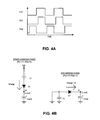
- FIG. 4A is a timing diagram illustrating non-overlapping clock signals, in accordance with an embodiment of the invention.
- FIG. 4B includes two phase diagrams illustrating operation of a switching capacitor circuit, in accordance with an embodiment of the invention.
- FIG. 5 is a flow chart illustrating operation of a capacitive sensor with a sigma-delta modulator, in accordance with an embodiment of the invention.
- FIG. 6 is circuit diagram of a capacitive sensor with a sigma-delta modulator, in accordance with an embodiment of the invention.
- FIG. 7 is a circuit diagram illustrating pin-out connections for implementing a single field sensor interface, in accordance with an embodiment of the invention.
- FIG. 8 is a circuit diagram illustrating pin-out connections for implementing a multi-field sensor interface time sharing a single sigma-delta modulator, in accordance with an embodiment of the invention.
- FIG. 9 is a functional block diagram illustrating a demonstrative processing system for implementing a capacitive sense user interface, in accordance with an embodiment of the invention.
- FIGS. 10A-C are circuit diagrams illustrating alternative dissipation circuit implementations within a sigma-delta modulator, in accordance with embodiments of the invention.
- Embodiments of an apparatus and method for a capacitive sensor with a sigma-delta modulator are described herein.
- numerous specific details are set forth to provide a thorough understanding of the embodiments.
- One skilled in the relevant art will recognize, however, that the techniques described herein can be practiced without one or more of the specific details, or with other methods, components, materials, etc.
- well-known structures, materials, or operations are not shown or described in detail to avoid obscuring certain aspects.
- FIG. 2 is a circuit diagram illustrating a capacitive sensor 200 , in accordance with an embodiment of the invention.
- Capacitive sensor 200 is capable of converting the measurement of the capacitance of sensing capacitor (Cx) into the measurement of the duty cycle of a feedback pulse signal (FB SIG). Furthermore, the relationship between the duty cycle of FB SIG and the capacitance of Cx is substantially linear.
- Capacitive sensor 200 may also be regarded as a switching capacitor current to duty cycle converter.
- the illustrated embodiment of capacitance sensor 200 includes a switching capacitor circuit 205 , sigma-delta modulator 210 , a measurement circuit 215 , logic 217 , and a control circuit 220 .
- the illustrated embodiment of switching capacitor circuit 205 includes sensing capacitor (Cx), switches SW 1 , SW 2 , and SW 3 , a diode D 1 , and a modulation capacitor (Cmod).
- the illustrated embodiment of sigma-delta modulator 210 includes a comparator (CMP) 225 , a latch 230 , a clock source 235 , a discharge resistor (Rd), and a discharge switch SW 4 .
- the discharge resistor Rd and discharge switch SW 4 may be referred to as a charge dissipation circuit 227 . While component values of switching capacitor circuit 205 and sigma-delta modulator 210 may vary based on the particular application, in general, the capacitance of Cmod will be substantially larger than the capacitance of Cx. Since Cmod acts to accumulate charge transferred from Cx over multiple cycles, it is often referred to as a summing capacitor or an integrating capacitor. In one embodiment, comparator 225 is an analog voltage comparator.
- FIG. 3 is a diagram illustrating operation of a capacitive field sensor 300 , in accordance with an embodiment of the invention.
- Capacitive field sensor 300 may be used to implement a user interface of an electronic device.
- Capacitive field sensor 300 is one possible physical implementation of sense capacitor Cx.
- the illustrated embodiment of capacitive field sensor 300 is made of two interlocking combs 305 and 310 on a printed circuit board (PCB) substrate. Each comb has a capacitance represented as CA while the finger has a variable capacitance represented as CF.
- the sense capacitance Cx represents the capacitance divider circuit 315 formed when the finger is brought into proximity with capacitive field sensor 300 .
- logic 217 includes hardware and/or software logic for deciding when a significant change in the duty cycle of FB_SIG should be recognized as a valid finger interaction with capacitive field sensor 300 .
- FIGS. 4A and 4B illustrate the two non-overlapping phase operation of switching capacitor circuit 205 , in accordance with an embodiment of the invention.
- two configuration phases of switching capacitor circuit 205 are cycled through to perform capacitive sensing.
- the two phases include: a series charging phase (control signal Phi 1 asserted) and a discharge phase (control signal Phi 2 asserted).
- control signals Phi 1 and Phi 2 are generated by control circuit 220 based on a single clock signal CLK.
- Phi 1 and Phi 2 are generated as non-overlapping pulse signals sufficiently spaced to prevent cross conduction or latch up between SW 1 , SW 2 , and SW 3 .
- This configuration couples sensing capacitor Cx in series with modulation capacitor Cmod.
- a charging current Icharge flows from the power source Vdd to ground through Cx, D 1 , and Cmod causing Cx and Cmod to charge.
- diode D 1 conducts Icharge in a forward biased operating regime.
- Phi 1 open circuits SW 1 and close circuits SW 2 and SW 3 .
- This configuration disconnects the power source Vdd, while coupling both terminals of sensing capacitor Cx to ground to discharge the sensing capacitor.
- This configuration also reverse biases diode D 1 , which prevents Cmod from discharging. Accordingly, the voltage Umod at node N 1 is held during the discharging phase.
- the variable capacitance of Cx is increased causing less charge to be passed to Cmod during each series charging phase. The greater charge captured by Cx during the charging phase is discharged to ground during the discharge phase. Therefore, the larger Cx, the greater the number of switching cycles of SW 1 , SW 2 , and SW 3 to charge Cmod to a given voltage.
- the voltage Umod continuously dithers back and forth about Vref generating a square wave at the output latch 230 .
- This square wave is analyzed by measurement circuit 215 to determine the duty cycle or percentage of time FB_SIG is high versus low. This percentage averaged over time is representative of the capacitance or capacitance change of sensing capacitor Cx.
- FIGS. 10A-C are circuit diagrams illustrating alternative implementations of charge dissipation circuit 227 within a sigma-delta modulator, in accordance with embodiments of the invention.
- FIG. 10A illustrates a sigma-delta modulator 211 having a charge dissipation circuit 228 , which replaces SW 4 and discharge resistor Rd of charge dissipation circuit 227 with a current source I D controlled by feedback pulse signal FB_SIG.
- FB_SIG is a logic HIGH
- the current source sinks a current I D from modulation capacitor Cmod to ground.
- FB_SIG is logic LOW
- the current source is disabled.
- FIG. 10B illustrates a sigma-delta modulator 212 having a charge dissipation circuit 229 including a switching capacitor resistor circuit with a gated clock source.
- FB SIG is logic HIGH
- the clock signal CLK is applied to the switches SW 5 and SW 6 with non-overlapping pulses (e.g., such as clock signals Phi 1 and Phi 2 generated by control circuit 220 ), causing a discharging current to flow to ground from modulation capacitor Cmod.
- the clock signal CLK is gated and switching capacitor circuit including Ccomp does not sink current from modulator capacitor Cmod.
- FIG. 10C illustrates a sigma-delta modulator 213 having a charge dissipation circuit 231 where the non-overlapping clock phases Phi 1 and Phi 2 are applied constantly to switches SW 5 and SW 6 , but SW 5 and SW 6 are selectively connected in series between Umod and either Vref or ground by the multiplexor MUX, depending on the value of the feedback pulse signal FB SIG.
- the principle of operation of charge dissipation circuit 231 is similar to charge dissipation circuit 229 in that SW 5 , SW 6 , and Ccomp operate as a switching capacitor resistor circuit.
- FIG. 5 is a flow chart illustrating operation of a capacitive sensor 200 in further detail, in accordance with an embodiment of the invention.
- the order in which some or all of the process blocks appear in process 500 should not be deemed limiting. Rather, one of ordinary skill in the art having the benefit of the present disclosure will understand that some of the process blocks may be executed in a variety of orders not illustrated, or even in parallel.
- capacitance sensor 200 is powered on and the output of CMP 210 (MOD_SIG) is initially low, assuming Cmod is initially discharged and the voltage Umod is less than Vref. In this state, MOD_SIG is logic “LOW”.
- latch 230 latches the value of MOD_SIG to its output. This output is fed back to the control terminal of switch SW 4 as feedback signal FB_SIG.
- a logic LOW open circuits SW 4 decoupling node N 1 from ground (process block 510 ) and permitting Cmod to accumulate charge.
- switches SW 1 , SW 2 , and SW 3 commence operation (process block 515 ).
- Switches SW 1 , SW 2 , and SW 3 switch under control of a control signals Phi 1 and Phi 2 generated by control circuit 220 , as discussed above.
- the voltage potential Umod at node N 1 begins to rise gradually.
- Cmod continues to accumulate charge until Umod reaches Vref, as determined by CMP 225 (decision block 520 ).
- CMP 225 toggles its output (MOD_SIG) to a logic “HIGH” (process block 525 ).
- latch 230 latches the value of MOD_SIG to its output as FB_SIG. Latching is synchronized to a clock signal output by clock source 235 .
- FB_SIG is fed back to discharge switch SW 4 .
- the toggled value is a logic HIGH, which close circuits discharging switch SW 4 and commences discharge of Cmod through Rd (process block 535 ).
- Cmod is discharged until Umod drops back below Vref, as determined by CMP 225 (decision block 540 ), at which point CMP 225 toggles MOD-SIG (process block 545 ).
- Discharge switch SW 4 is once again open circuited after MOD_SIG is latched and process 500 repeats from process block 510 .
- capacitance sensor 200 After an initial transitory startup phase, capacitance sensor 200 enters its steady state phase where the voltage potential Umod on Cmod oscillates or dithers about Vref. This oscillation about Vref creates the modulation signal MOD_SIG upon which the feedback pulse signal FB_SIG is based. Once operating in the steady state phase, the duty cycle of the FB SIG is directly proportional to the capacitance or capacitance change of Cx.
- the duty cycle of FB_SIG is measured by measurement circuit 215 .
- measurement circuit 215 may include a clock gated by FB_SIG and a counter to count a number of clock cycles occurring while FB_SIG is HIGH for a given period of time.
- the measured duty cycle is used to determine the capacitance Cx or capacitance change ACx of the sensing capacitor.
- Logic 217 may use this digital code to determine whether a user finger has interacted with a capacitive field sensor within a user interface.
- measurement circuit 215 may output a digital code indicative of the capacitance or capacitance change of Cx.
- capacitive sensor 200 operates as a Cmod charge current (i.e., Icharge in FIG. 4B ) to digital code converter.
- the charge current of Cmod is related to the variable capacitance of the field sensor Cx.
- FIG. 6 is a circuit diagram of a capacitive sensor 600 including a sigma-delta modulator, in accordance with an embodiment of the invention.
- Capacitive sensor 600 is an alternative embodiment to capacitive sensor 200 , but operates using the same principles.
- the illustrated embodiment of capacitive sensor 600 includes a switching capacitor circuit 605 , a sigma-delta modulator 210 , measurement circuit 215 , and a clock source 620 .
- the illustrated embodiment of switching capacitor circuit 605 includes sensing capacitor Cx, a filter resistor Rfilt, diode D 1 , modulation capacitor Cmod, a discharge switch SW 5 , and an inverter INV 1 .
- clock source 620 is a pseudo-random signal (PRS) generator for generating a pseudo-random pulse signal.
- PRS pseudo-random signal
- Other signal generators maybe used, such as a pulse width modulator; however, a PRS generator provides greater electromagnetic noise immunity.
- frequency spreading techniques can also be used to implement clock source 620 , such as frequency sweeping, frequency hopping, changing frequency in the pseudo random order, etc.
- Sigma-delta modulator 210 and measurement circuit 215 operate as discussed above in connection with capacitive sensor 200 .
- switching capacitor circuit 605 operates to sequentially charge Cmod, just as switching capacitor circuit 205 , with a slight variation on its specific implementation.
- clock source 620 outputs a logic HIGH
- diode D 1 is forward biased and switch SW 5 is open circuited.
- the open circuited SW 5 connects Cmod in series with Cx and clock source 620 .
- the forward biased D 1 permits a charging current to flow through sensing capacitor Cx and filter resistor Rfilt into modulation capacitor Cmod.
- clock source 620 is logic HIGH, switching capacitor circuit 605 is in the “charging phase.”
- switch SW 5 When clock source 620 transitions to a logic LOW, switch SW 5 is closed circuited. The closed circuited SW 5 connects node N 2 to ground. This couples sensing capacitor Cx to ground through Rfilt and reverse biases diode D 1 . With Cx coupled to ground it discharges, while the reversed biased diode D 1 prevents discharge from modulation capacitor Cmod and Cmod retains its voltage Umod. While clock source 620 is logic LOW, switching capacitor circuit 605 is in the “discharge phase.”
- filter resistor Rfilt and switch SW 5 coupled to ground creates a high frequency cutoff low pass filter (LPF).
- LPF high frequency cutoff low pass filter
- FIG. 7 is a circuit diagram illustrating pin-out connections for implementing a single field sensor interface 700 within an integrated circuit, in accordance with an embodiment of the invention.
- Integrated circuit (“IC”) 705 includes sigma-delta modulator 210 , clock source 620 , inverter INV 1 , and switch SW 5 integrated on a single die. The following components including: sensing capacitor Cx, filter resistor Rfilt, discharge resistor Rd, modulation capacitor Cmod, and diode D 1 are externally coupled to IC 705 .
- inverter INV 1 may be implemented in software or firmware using a look up table (“LUT”).
- LUT look up table
- FIG. 8 is a circuit diagram illustrating pin-out connections for implementing a multi field sensor interface 800 within an integrated circuit, in accordance with an embodiment of the invention.
- IC 805 couples multiple field sensors Cx 1 and Cx 2 to a single general purpose input/output (“GPIO”) pin 810 .
- Field sensors Cx 1 and Cx 2 time share a single GPIO 810 , clock source 620 , and sigma-delta modulator 210 .
- each externally coupled sensor includes its own externally coupled filter resistor (e.g., Rfilt 1 , Rfilt 2 ) and its own internal switch SW 5 (e.g., SW 5 A, SW 5 B).
- Each field sensor Cx 1 or Cx 2 is scanned one at a time via appropriate switching of the select switches SEL 1 and SEL 2 .
- Select switches SEL 1 and SEL 2 either activate the control terminals of switches SW 5 A and SW 5 B thereby grounding the corresponding field sensors Cx 1 or Cx 2 , or connect the control terminal to the output of inverter INV 1 .
- FIG. 8 illustrates just two field sensors Cx 1 and Cx 2 , it should be appreciated that a large number of field sensors can thus timeshare GPIO pin 810 .
- FIG. 9 is a functional block diagram illustrating a demonstrative system 1100 for implementing a capacitive sense user interface, in accordance with an embodiment of the invention.
- the illustrated embodiment of system 1100 includes a processing device 1110 , a capacitive sense pad 1120 , a capacitive sense linear slider 1130 , a capacitive sense radial slider 1140 , a host processor 1150 , an embedded controller 1160 , and non-capacitance sensor elements 1170 .
- Processing device 1110 may include analog and/or digital general purpose input/output (“GPIO”) ports 1107 .
- GPIO general purpose input/output
- GPIO ports 1107 may be programmable. GPIO ports 1107 may be coupled to a Programmable Interconnect and Logic (“PIL”), which acts as an interconnect between GPIO ports 1107 and a digital block array of processing device 1110 (not illustrated).
- PIL Programmable Interconnect and Logic
- the digital block array may be configured to implement a variety of digital logic circuits (e.g., DAC, digital filters, digital control systems, etc.) using, in one embodiment, configurable user modules (“UMs”).
- the digital block array may be coupled to a system bus.
- Processing device 1110 may also include memory, such as random access memory (RAM) 1105 and program flash 1104 .
- RAM 1105 may be static RAM (“SRAM”), and program flash 1104 may be a non-volatile storage, which may be used to store firmware.
- Processing device 1110 may also include a memory controller unit (“MCU”) 1103 coupled to memory and the processing core 1102 .
- MCU memory controller unit
- Processing device 1110 may also include an analog block array (not illustrated).
- the analog block array is also coupled to the system bus.
- the analog block array also may be configured to implement a variety of analog circuits (e.g., ADC, analog filters, etc.) using, in one embodiment, configurable UMs.
- the analog block array may also be coupled to the GPIO 1107 .
- capacitance sensor 1101 which includes an implementation of capacitance sensor 200 , 600 , 700 , or 800 may be integrated into processing device 1110 .
- Capacitance sensor 1101 may include analog 110 for coupling to an external component, such as capacitive sense pad 1120 , capacitive sense linear slider 1130 , capacitive sense radial slider 1140 , and/or other capacitive sense devices.
- Capacitive sense pad 1120 , capacitive sense linear slider 1130 , and/or capacitive sense radial slider 1140 may each include one or more sensing capacitors Cx to implement the individual capacitive sense buttons therein.
- Processing device 1110 may include internal oscillator/clocks 1106 and communication block 1108 .
- the oscillator/clocks block 1106 provides clock signals to one or more of the components of processing device 1110 .
- Communication block 1108 may be used to communicate with an external component, such as a host processor 1150 , via host interface (I/F) line 1151 .
- processing device 1110 may also be coupled to embedded controller 1160 to communicate with the external components, such as host 1150 .
- Interfacing to the host 1150 can be through various methods. In one exemplary embodiment, interfacing with the host 1150 may be done using a standard PS/2 interface to connect to embedded controller 1160 , which in turn sends data to the host 1150 via low pin count (LPC) interface.
- LPC low pin count
- processing device 1110 may do both touch-sensor pad and keyboard control operations, thereby freeing up the embedded controller 1160 for other housekeeping functions.
- interfacing may be done using a universal serial bus (USB) interface directly coupled to host 1150 via host interface line 1151 .
- processing device 1110 may communicate to external components, such as host 1150 using industry standard interfaces, such as USB, PS/2, inter-integrated circuit (I2C) bus, or system packet interfaces (SPI).
- Host 1150 and/or embedded controller 1160 may be coupled to processing device 1110 with a ribbon or flex cable from an assembly, which houses the sensing device and processing device.
- processing device 1110 is configured to communicate with embedded controller 1160 or host 1150 to send and/or receive data.
- the data may be a command or alternatively a signal.
- system 1100 may operate in both standard-mouse compatible and enhanced modes.
- the standard-mouse compatible mode utilizes the HID class drivers already built into the Operating System (OS) software of host 1150 . These drivers enable processing device 1110 and sensing device to operate as a standard cursor control user interface device, such as a two-button PS/2 mouse.
- the enhanced mode may enable additional features such as scrolling (reporting absolute position) or disabling the sensing device, such as when a mouse is plugged into the notebook.
- processing device 1110 may be configured to communicate with embedded controller 1160 or host 1150 , using nonOS drivers, such as dedicated touch-sensor pad drivers, or other drivers known by those of ordinary skill in the art.
- Processing device 1110 may reside on a common carrier substrate such as, for example, an integrated circuit (IC) die substrate, a multi-chip module substrate, or the like. Alternatively, the components of processing device 1110 may be one or more separate integrated circuits and/or discrete components. In one exemplary embodiment, processing device 1110 may be a Programmable System on a Chip (PSoCTM) processing device, manufactured by Cypress Semiconductor Corporation, San Jose, Calif. Alternatively, processing device 1110 may be one or more other processing devices known by those of ordinary skill in the art, such as a microprocessor or central processing unit, a controller, special-purpose processor, digital signal processor (“DSP”), an application specific integrated circuit (“ASIC”), a field programmable gate array (“FPGA”), or the like. In an alternative embodiment, for example, processing device 1110 may be a network processor having multiple processors including a core unit and multiple microengines. Additionally, processing device 1110 may include any combination of general-purpose processing device(s) and special-purpose processing device(s).
- Capacitance sensor 1101 may be integrated into the IC of processing device 1110 , or alternatively, in a separate IC. Descriptions of capacitance sensor 1101 may be generated and compiled for incorporation into other integrated circuits. For example, behavioral level code describing capacitance sensor 1101 , or portions thereof, may be generated using a hardware descriptive language, such as VHDL or Verilog, and stored to a machine-accessible medium (e.g., CD-ROM, hard disk, floppy disk, etc.). Furthermore, the behavioral level code can be compiled into register transfer level (“RTL”) code, a netlist, or even a circuit layout and stored to a machine-accessible medium. The behavioral level code, the RTL code, the netlist, and the circuit layout all represent various levels of abstraction to describe capacitance sensor 1101 .
- VHDL hardware descriptive language
- Verilog machine-accessible medium
- RTL register transfer level
- electronic system 1100 may be used in a notebook computer.
- system 1100 may be used in other applications, such as a mobile handset, a personal data assistant (PDA), a keyboard, a television, a remote control, a monitor, a handheld multi-media device, a handheld video player, a handheld gaming device, or a control panel.
- PDA personal data assistant
- a machine-accessible medium includes any mechanism that provides (e.g., stores) information in a form accessible by a machine (e.g., a computer, network device, personal digital assistant, manufacturing tool, any device with a set of one or more processors, etc.).
- a machine-accessible medium includes recordable/non-recordable media (e.g., read only memory (ROM), random access memory (RAM), magnetic disk storage media, optical storage media, flash memory devices, etc.).
Abstract
Description
where Vcsum represents the voltage on Csum, N represents the cycle count, Cx and Csum represent capacitance values, and Vdd represents a power supply voltage. Accordingly, the capacitance of Cx can be determined by measuring the number of cycles (or time) required to raise Csum to a predetermined voltage potential.
Claims (17)
Priority Applications (1)
| Application Number | Priority Date | Filing Date | Title |
|---|---|---|---|
| US13/342,942 US9400298B1 (en) | 2007-07-03 | 2012-01-03 | Capacitive field sensor with sigma-delta modulator |
Applications Claiming Priority (3)
| Application Number | Priority Date | Filing Date | Title |
|---|---|---|---|
| US94786507P | 2007-07-03 | 2007-07-03 | |
| US12/167,100 US8089289B1 (en) | 2007-07-03 | 2008-07-02 | Capacitive field sensor with sigma-delta modulator |
| US13/342,942 US9400298B1 (en) | 2007-07-03 | 2012-01-03 | Capacitive field sensor with sigma-delta modulator |
Related Parent Applications (1)
| Application Number | Title | Priority Date | Filing Date |
|---|---|---|---|
| US12/167,100 Division US8089289B1 (en) | 2007-07-03 | 2008-07-02 | Capacitive field sensor with sigma-delta modulator |
Publications (1)
| Publication Number | Publication Date |
|---|---|
| US9400298B1 true US9400298B1 (en) | 2016-07-26 |
Family
ID=45374592
Family Applications (2)
| Application Number | Title | Priority Date | Filing Date |
|---|---|---|---|
| US12/167,100 Active 2029-06-19 US8089289B1 (en) | 2007-07-03 | 2008-07-02 | Capacitive field sensor with sigma-delta modulator |
| US13/342,942 Active 2031-03-08 US9400298B1 (en) | 2007-07-03 | 2012-01-03 | Capacitive field sensor with sigma-delta modulator |
Family Applications Before (1)
| Application Number | Title | Priority Date | Filing Date |
|---|---|---|---|
| US12/167,100 Active 2029-06-19 US8089289B1 (en) | 2007-07-03 | 2008-07-02 | Capacitive field sensor with sigma-delta modulator |
Country Status (1)
| Country | Link |
|---|---|
| US (2) | US8089289B1 (en) |
Cited By (2)
| Publication number | Priority date | Publication date | Assignee | Title |
|---|---|---|---|---|
| US10025441B2 (en) | 2007-07-03 | 2018-07-17 | Cypress Semiconductor Corporation | Capacitive field sensor with sigma-delta modulator |
| WO2022184494A1 (en) * | 2021-03-02 | 2022-09-09 | Vitesco Technologies GmbH | Capacitive sensor with optimized noise immunity |
Families Citing this family (109)
| Publication number | Priority date | Publication date | Assignee | Title |
|---|---|---|---|---|
| US8144125B2 (en) | 2006-03-30 | 2012-03-27 | Cypress Semiconductor Corporation | Apparatus and method for reducing average scan rate to detect a conductive object on a sensing device |
| US8547114B2 (en) | 2006-11-14 | 2013-10-01 | Cypress Semiconductor Corporation | Capacitance to code converter with sigma-delta modulator |
| US8144126B2 (en) | 2007-05-07 | 2012-03-27 | Cypress Semiconductor Corporation | Reducing sleep current in a capacitance sensing system |
| US8169238B1 (en) | 2007-07-03 | 2012-05-01 | Cypress Semiconductor Corporation | Capacitance to frequency converter |
| US8089289B1 (en) | 2007-07-03 | 2012-01-03 | Cypress Semiconductor Corporation | Capacitive field sensor with sigma-delta modulator |
| US8525798B2 (en) | 2008-01-28 | 2013-09-03 | Cypress Semiconductor Corporation | Touch sensing |
| US8358142B2 (en) | 2008-02-27 | 2013-01-22 | Cypress Semiconductor Corporation | Methods and circuits for measuring mutual and self capacitance |
| US8319505B1 (en) | 2008-10-24 | 2012-11-27 | Cypress Semiconductor Corporation | Methods and circuits for measuring mutual and self capacitance |
| US9104273B1 (en) | 2008-02-29 | 2015-08-11 | Cypress Semiconductor Corporation | Multi-touch sensing method |
| US8321174B1 (en) | 2008-09-26 | 2012-11-27 | Cypress Semiconductor Corporation | System and method to measure capacitance of capacitive sensor array |
| US8362784B2 (en) * | 2009-06-22 | 2013-01-29 | Mitsubishi Electric Corporation | Capacitor capacitance diagnosis device and electric power apparatus equipped with capacitor capacitance diagnosis device |
| US20110084711A1 (en) * | 2009-10-08 | 2011-04-14 | Sitronix Technology Corp. | Capacitance sensing circuit with anti-electromagnetic interference capability |
| US8344928B2 (en) * | 2010-11-10 | 2013-01-01 | Stmicroelectronics Asia Pacific Pte Ltd. | Method and apparatus for capacitance sensing |
| DE102011002447B4 (en) * | 2011-01-04 | 2014-07-10 | Ident Technology Ag | Capacitive proximity sensor and capacitive proximity detection method |
| DE102011002446A1 (en) * | 2011-01-04 | 2012-07-05 | Ident Technology Ag | Sensor device and method for capacitive proximity detection |
| US9876510B2 (en) | 2013-02-28 | 2018-01-23 | Christoph HELDEIS | Method for determining active input elements of an input arrangement and input arrangement |
| US9587964B2 (en) | 2013-06-12 | 2017-03-07 | Microchip Technology Incorporated | Capacitive proximity detection using delta-sigma conversion |
| JP6203549B2 (en) | 2013-06-27 | 2017-09-27 | ルネサスエレクトロニクス株式会社 | Semiconductor device |
| JP6224438B2 (en) | 2013-11-26 | 2017-11-01 | ルネサスエレクトロニクス株式会社 | Semiconductor device |
| GB2521416B (en) * | 2013-12-19 | 2017-02-01 | Cirrus Logic Int Semiconductor Ltd | Biasing circuitry for MEMS transducers |
| US10444862B2 (en) | 2014-08-22 | 2019-10-15 | Synaptics Incorporated | Low-profile capacitive pointing stick |
| WO2016155943A1 (en) | 2015-03-30 | 2016-10-06 | Koninklijke Philips N.V. | A method and system for sensing a liquid level |
| KR101739791B1 (en) * | 2015-05-11 | 2017-05-26 | 주식회사 하이딥 | Pressure sensor, pressure detector and touch input device including the same |
| US9864455B2 (en) | 2015-05-29 | 2018-01-09 | Synaptics Incorporated | Matched filter for a first order sigma delta capacitance measurement system and a method to determine the same |
| US11397492B2 (en) | 2015-06-22 | 2022-07-26 | Sigmasense, Llc. | Enhanced mutual capacitance touch screen display with shape detection and methods for use therewith |
| KR101909515B1 (en) | 2015-06-22 | 2018-10-18 | 시그마센스, 엘엘씨. | Multi-touch sensor and electrostatic pen digitizing system utilizing simultaneous functions for improved performance |
| US11907484B2 (en) | 2015-06-22 | 2024-02-20 | Sigmasense, Llc. | Function and orientation identification for input/output (I/O) operative touch sensor device (TSD) |
| US11269455B1 (en) | 2020-10-23 | 2022-03-08 | Sigmasense, Llc. | Enhanced mutual capacitance touch screen display with noise compensation and methods for use therewith |
| US10664098B2 (en) | 2015-06-22 | 2020-05-26 | Sigmasense, Llc. | Channel driver circuit |
| JP6551915B2 (en) | 2015-07-06 | 2019-07-31 | シグマセンス,エルエルシー | Pen system for internal pressure, tilt and rotation |
| US10175837B2 (en) * | 2015-10-31 | 2019-01-08 | Cirque Corporation | Offset charge injection for increasing measurement security |
| US10061415B2 (en) | 2016-06-30 | 2018-08-28 | Synaptics Incorporated | Input device receiver with delta-sigma modulator |
| EP3273231A1 (en) * | 2016-07-22 | 2018-01-24 | Ostbayerische Technische Hochschule Regensburg | Arrangement for measuring capacitance |
| US11246507B2 (en) | 2016-08-18 | 2022-02-15 | Sigmasense, Llc. | Wireless in-shoe physical activity monitoring apparatus |
| US10162467B2 (en) * | 2017-03-08 | 2018-12-25 | Cypress Semiconductor Corporation | Ratiometric mutual-capacitance-to-code converter |
| US10838530B2 (en) | 2017-09-15 | 2020-11-17 | Sigmasense, Llc. | Touchscreen display with concurrent touch and display operations |
| US11003205B2 (en) | 2019-02-04 | 2021-05-11 | Sigmasense, Llc. | Receive analog to digital circuit of a low voltage drive circuit data communication system |
| US11429226B2 (en) | 2018-08-27 | 2022-08-30 | Sigmasense, Llc. | Analog-digital drive sense circuit |
| US10895867B2 (en) | 2018-08-27 | 2021-01-19 | Sigmasense, Llc. | Analog world interfacing for automated systems |
| US11513543B2 (en) | 2018-08-27 | 2022-11-29 | Sigmasense, Llc. | Impedance detect drive sense circuit |
| US10554215B1 (en) | 2019-03-26 | 2020-02-04 | Sigmasense, Llc. | Analog to digital conversion circuit with very narrow bandpass digital filtering |
| US11550426B2 (en) | 2018-08-27 | 2023-01-10 | Sigmasense, Llc. | Sensor monitoring system |
| US11635396B2 (en) | 2018-08-27 | 2023-04-25 | Sigmasense, Llc. | Sensing device with drive sense circuit and particle sensor and methods for use therewith |
| US11099032B2 (en) | 2018-08-27 | 2021-08-24 | Sigmasense, Llc. | Drive sense circuit with drive-sense line |
| US11822358B2 (en) | 2018-08-27 | 2023-11-21 | Sigmasense, Llc. | Drive-sense circuit to determine effects of different electrical characteristics on load |
| US11644860B2 (en) | 2018-08-27 | 2023-05-09 | Sigmasense, Llc. | Configuring a programmable drive sense unit |
| US11914812B2 (en) | 2018-08-27 | 2024-02-27 | Sigmasense, Llc. | Current reference operative drive-sense circuit (DSC) |
| US10845985B2 (en) | 2018-09-14 | 2020-11-24 | Sigmasense, Llc. | Identification in touch systems |
| US10908718B2 (en) | 2018-09-14 | 2021-02-02 | Sigmasense, Llc. | Large touch screen display with integrated electrodes |
| US11875005B2 (en) | 2018-09-14 | 2024-01-16 | Sigmasense, Llc. | Touch screen display with touchless indications and methods for use therewith |
| US11789555B2 (en) | 2018-09-14 | 2023-10-17 | Sigmasense, Llc. | Touch sense control circuit with noise suppression |
| US11899867B2 (en) | 2018-09-14 | 2024-02-13 | Sigmasense, Llc. | Touch screen display with touchless gestures and methods for use therewith |
| US11372510B2 (en) | 2018-11-02 | 2022-06-28 | Sigmasense, Llc. | Multi-conductor touch system |
| US10852857B2 (en) | 2018-11-19 | 2020-12-01 | Sigmasense, Llc. | Frequency diverse e-pen for touch sensor and e-pen systems |
| US10935585B2 (en) | 2018-11-19 | 2021-03-02 | Sigmasense, Llc. | Drive sense circuit with transient suppression |
| US10996728B2 (en) | 2019-01-04 | 2021-05-04 | Sigmasense, Llc. | Power supply signal conditioning system based on drive-sense circuit (DSC) processing |
| US10826747B2 (en) | 2019-01-14 | 2020-11-03 | Sigmasense, Llc. | Low voltage drive circuit with digital to digital conversion and methods for use therewith |
| US10831690B2 (en) | 2019-01-14 | 2020-11-10 | Sigmasense, Llc. | Channel allocation among low voltage drive circuits |
| US11327917B2 (en) | 2019-01-14 | 2022-05-10 | Sigmasense, Llc. | Low voltage drive circuit and communication system |
| US10915483B2 (en) | 2019-01-14 | 2021-02-09 | Sigmasense, Llc. | Low voltage drive circuit with variable oscillating characteristics and methods for use therewith |
| US10684977B1 (en) | 2019-01-14 | 2020-06-16 | Sigmasense, Llc. | Low voltage drive circuit with bus isolation and methods for use therewith |
| US10884967B2 (en) | 2019-01-14 | 2021-01-05 | Sigmasense, Llc. | Low voltage drive circuit with variable frequency characteristics and methods for use therewith |
| US10831226B2 (en) | 2019-01-14 | 2020-11-10 | Sigmasense, Llc | Low voltage drive circuit with variable oscillating frequencies and methods for use therewith |
| US10733133B1 (en) | 2019-01-14 | 2020-08-04 | Sigmasense, Llc. | Low voltage drive circuit with range limits and methods for use therewith |
| US11061082B2 (en) | 2019-03-18 | 2021-07-13 | Sigmasense, Llc. | Single line hall effect sensor drive and sense |
| US10671034B1 (en) | 2019-03-18 | 2020-06-02 | Sigmasense, Llc. | Motor drive input adaptation with in-line drive-sense circuit |
| US11029782B2 (en) | 2019-05-03 | 2021-06-08 | Sigmasense, Llc. | Light emitting diode (LED) touch display circuit |
| JP7113139B2 (en) | 2019-05-10 | 2022-08-04 | 株式会社ワコム | Method for transmitting transmission data from sensor controller to pen, and pen |
| US11056930B2 (en) | 2019-05-31 | 2021-07-06 | Sigmasense, Llc. | Wireless power transfer and communications |
| US10756578B1 (en) | 2019-05-31 | 2020-08-25 | Sigmasense, Llc. | Wireless power transfer with in-line sensing and control |
| US11131714B2 (en) | 2019-05-31 | 2021-09-28 | Sigmasense, Llc. | Battery monitoring and characterization during charging |
| US11126297B2 (en) | 2019-06-10 | 2021-09-21 | Sigmasense, Llc. | Electronic pen with ring-back and other functionalities |
| US11221709B2 (en) | 2019-06-10 | 2022-01-11 | Sigmasense, Llc. | Electronic writing apparatus with ring-back and other functionalities |
| US11216133B2 (en) | 2019-06-10 | 2022-01-04 | Sigmasense, Llc. | Device for use with a touch screen |
| US11054920B2 (en) | 2019-06-10 | 2021-07-06 | Sigmasense, Llc. | Pen for use with a touch screen |
| US11029769B2 (en) | 2019-06-10 | 2021-06-08 | Sigmasense, Llc. | Pen for use with a touch screen |
| US11555687B2 (en) | 2019-08-08 | 2023-01-17 | Sigmasense, Llc. | Capacitive imaging glove |
| US10976837B2 (en) | 2019-08-20 | 2021-04-13 | Sigmasense, Llc. | User input passive device for use with an interactive display device |
| US11017845B2 (en) | 2019-09-11 | 2021-05-25 | Sigmasense, Llc. | RAM cell processing circuit for concurrency of refresh and read |
| US10908641B1 (en) | 2019-10-09 | 2021-02-02 | Sigmasense, Llc. | Display generated data transmission from user device to touchscreen via user |
| US11221980B2 (en) | 2019-10-31 | 2022-01-11 | Sigmasense, Llc. | Low voltage drive circuit operable to convey data via a bus |
| US11190205B2 (en) | 2019-11-08 | 2021-11-30 | Sigmasense, Llc. | Single-ended direct interface dual DAC feedback photo-diode sensor |
| US10862492B1 (en) * | 2019-11-08 | 2020-12-08 | Sigmasense, Llc. | Current operative analog to digital converter (ADC) |
| US11133811B2 (en) | 2019-11-08 | 2021-09-28 | Sigmasense, Llc. | High resolution analog to digital converter (ADC) with improved bandwidth |
| US11709189B2 (en) | 2019-11-08 | 2023-07-25 | Sigmasense, Llc. | Two-element high accuracy impedance sensing circuit with increased signal to noise ratio (SNR) |
| US11935397B2 (en) | 2019-12-30 | 2024-03-19 | Sigmasense, Llc. | Organic and inorganic test system |
| US11216109B2 (en) | 2020-01-07 | 2022-01-04 | Sigmasense, Llc. | Drive-sense control for extended sensor panels |
| US11221704B2 (en) | 2020-02-05 | 2022-01-11 | Sigmasense, Llc. | Screen-to-screen communication via touch sense elements |
| US11079888B1 (en) | 2020-02-18 | 2021-08-03 | Sigmasense, Llc. | Sensitivity region of interest processing (ROIP) for input/output (I/O) operative touch sensor device (TSD) |
| US11144160B1 (en) | 2020-03-30 | 2021-10-12 | Sigmasense, Llc. | Three-dimensional data reduction method and system |
| US11182038B2 (en) | 2020-04-08 | 2021-11-23 | Sigmasense, Llc. | Encoded data pattern touchscreen sensing system |
| US11340995B2 (en) | 2020-05-21 | 2022-05-24 | Sigmasense, Llc. | Integrated circuit with programmable input/output module |
| US11439812B2 (en) | 2020-06-03 | 2022-09-13 | Sigmasense, Llc. | Array operative to perform distributed/patterned sensing and/or stimulation across patient bodily section |
| US11504535B2 (en) | 2020-06-03 | 2022-11-22 | Sigmasense, Llc. | Pacemaker operative to deliver impulses of pace signal and sense cardiac response via single conductor of pacemaker lead |
| US11304002B2 (en) | 2020-08-12 | 2022-04-12 | Sigmasense, Llc. | Single transducer audio in/out device |
| US11442578B2 (en) * | 2020-08-31 | 2022-09-13 | Cypress Semiconductor Corporation | Ratio-metric multi-sensing convertor |
| US11374587B1 (en) | 2021-02-25 | 2022-06-28 | Sigmasense, Llc. | Batteryless wireless sensor system |
| US11575851B2 (en) | 2021-05-28 | 2023-02-07 | Sigmasense, Llc. | Handheld communication device with drive-sense circuit based imaging array and methods for use therewith |
| US11575850B2 (en) | 2021-05-28 | 2023-02-07 | Sigmasense, Llc. | Imaging device with drive-sense circuit(s) and methods for use therewith |
| US11679678B2 (en) | 2021-06-28 | 2023-06-20 | Sigmasense, Llc. | Vehicle system for detecting and visually conveying vehicle button interaction |
| US11733818B2 (en) | 2021-07-19 | 2023-08-22 | Sigmasense, Llc. | Identifying capacitively coupled devices |
| US11556298B1 (en) | 2021-07-30 | 2023-01-17 | Sigmasense, Llc | Generation and communication of user notation data via an interactive display device |
| US11592874B1 (en) | 2021-08-04 | 2023-02-28 | Sigmasense, Llc. | Touch sensing in a flexible/foldable touch screen display |
| US11467693B1 (en) * | 2021-08-06 | 2022-10-11 | Cypress Semiconductor Corporation | Impedance sensing methods |
| US11797139B2 (en) | 2021-09-21 | 2023-10-24 | Sigmasense, Llc. | Fingerprint scanning device incorporating drive-sense circuitry |
| US11435864B1 (en) | 2021-09-28 | 2022-09-06 | Sigmasense, Llc. | Differential touch screen display |
| US11709563B2 (en) | 2021-10-26 | 2023-07-25 | Sigmasense, Llc. | Touch-based device with interlaced electrode grids |
| US20230408580A1 (en) * | 2022-05-31 | 2023-12-21 | Taiwan Semiconductor Manufacturing Company, Ltd. | Device and Method for Measuring a Duty Cycle of a Clock Signal |
| US11740752B1 (en) | 2022-07-13 | 2023-08-29 | Sigmasense, Llc. | Device with signal generator |
Citations (121)
| Publication number | Priority date | Publication date | Assignee | Title |
|---|---|---|---|---|
| US3611024A (en) * | 1968-07-23 | 1971-10-05 | Matsushita Electric Ind Co Ltd | Semiconductor apparatus for controlling the brightness of a discharge lamp |
| US3660801A (en) | 1971-01-11 | 1972-05-02 | Noma World Wide Inc | One-piece socket for decorative light |
| US4277783A (en) | 1979-07-02 | 1981-07-07 | Bell Telephone Laboratories, Incorporated | Light pen tracking method and apparatus |
| US4510466A (en) | 1982-06-28 | 1985-04-09 | Gte Lenkurt Incorporated | Switched capacitor SSB modulator |
| US4558274A (en) | 1983-09-14 | 1985-12-10 | Johnson Service Company | Apparatus and method determining the value of a capacitance |
| US4686332A (en) | 1986-06-26 | 1987-08-11 | International Business Machines Corporation | Combined finger touch and stylus detection system for use on the viewing surface of a visual display device |
| US4878013A (en) | 1986-04-04 | 1989-10-31 | Mitutoyo Corporation | Capacitive type measurement transducer with improved electrode arrangement |
| US4896156A (en) * | 1988-10-03 | 1990-01-23 | General Electric Company | Switched-capacitance coupling networks for differential-input amplifiers, not requiring balanced input signals |
| US4977480A (en) | 1988-09-14 | 1990-12-11 | Fuji Koki Mfg. Co., Ltd. | Variable-capacitance type sensor and variable-capacitance type sensor system using the same |
| US5122755A (en) | 1990-05-11 | 1992-06-16 | New Sd, Inc. | Capacitive position detector |
| US5365461A (en) | 1992-04-30 | 1994-11-15 | Microtouch Systems, Inc. | Position sensing computer input device |
| US5386584A (en) | 1990-06-14 | 1995-01-31 | Chips And Technologies, Inc. | Interrupt-generating keyboard scanner using an image RAM |
| US5412387A (en) | 1993-04-06 | 1995-05-02 | Analog Devices, Inc. | Error reduction in switched capacitor digital-to-analog converter systems by balanced sampling |
| US5461321A (en) | 1993-09-17 | 1995-10-24 | Penberthy, Inc. | Apparatus and method for measuring capacitance from the duration of a charge-discharge charge cycle |
| US5479103A (en) | 1994-01-18 | 1995-12-26 | Air Communications, Inc. | Non-linear voltage measuring implementing capacitor charging time |
| US5495077A (en) | 1992-06-08 | 1996-02-27 | Synaptics, Inc. | Object position and proximity detector |
| US5525980A (en) | 1992-04-24 | 1996-06-11 | Sextant Avionique | Method and apparatus for operating a capacitive tactile keyboard |
| US5730165A (en) | 1995-12-26 | 1998-03-24 | Philipp; Harald | Time domain capacitive field detector |
| US5872561A (en) | 1997-03-31 | 1999-02-16 | Allen-Bradley Company, Llc | Fast scanning switch matrix |
| US5949264A (en) | 1996-11-29 | 1999-09-07 | Lo; Dennis C. | Digital phase detector and charge pump system reset and balanced current source matching methods and systems |
| US6008660A (en) | 1996-08-22 | 1999-12-28 | International Business Machines Corporation | Method for developing circuit capacitance measurements corrected for stray capacitance |
| US6278283B1 (en) | 1998-05-11 | 2001-08-21 | Mitsubishi Denki Kabushiki Kaisha | Capacitance detecting circuit |
| US20010048313A1 (en) | 2000-06-06 | 2001-12-06 | Peter Frank | Motion sensors |
| US20020008543A1 (en) | 2000-07-17 | 2002-01-24 | Koji Nasu | Load capacitance measuring circuit and output buffer adaptive to wide range of load capacitance |
| US6400217B1 (en) | 1999-09-28 | 2002-06-04 | Koninklijke Philips Electronics N.V. | Integrated circuit having a filter with charge balancing scheme to reduce transient disturbances |
| US20020080014A1 (en) | 2000-11-16 | 2002-06-27 | Mccarthy Kevin C. | Vehicle compartment occupancy detection system |
| US6449195B1 (en) | 2000-09-28 | 2002-09-10 | Motorola, Inc. | Method and apparatus for coupling noise reduction in a semiconductor device |
| US6448792B1 (en) | 1999-06-08 | 2002-09-10 | Nireco Corporation | Sensor for edge position of electro-conductive material |
| US6466036B1 (en) | 1998-11-25 | 2002-10-15 | Harald Philipp | Charge transfer capacitance measurement circuit |
| US6529015B2 (en) | 2000-03-02 | 2003-03-04 | Denso Corporation | Signal processing apparatus |
| US20030058053A1 (en) | 2001-09-25 | 2003-03-27 | Samsung Electronics Co., Ltd. | Phase locked loop for reducing electromagnetic interference |
| US20030112021A1 (en) | 2001-12-14 | 2003-06-19 | I F M Electronic Gmbh | Circuit arrangement for detecting the capacitance or capacitance change of a capacitive circuit element or component |
| US20030161278A1 (en) | 2002-02-25 | 2003-08-28 | Nec Corporation | Symbol data converting circuit |
| US20030184065A1 (en) | 1992-05-05 | 2003-10-02 | Breed David S. | Rear view mirror monitor |
| US20030189419A1 (en) | 2000-04-10 | 2003-10-09 | Ichiro Maki | Multiplex voltage measurement apparatus |
| US20030209893A1 (en) | 1992-05-05 | 2003-11-13 | Breed David S. | Occupant sensing system |
| US6690066B1 (en) | 2002-10-18 | 2004-02-10 | Texas Instruments Incorporated | Minimization and linearization of ESD parasitic capacitance in integrated circuits |
| US20040039298A1 (en) | 1996-09-04 | 2004-02-26 | Abreu Marcio Marc | Noninvasive measurement of chemical substances |
| US20040047110A1 (en) | 2000-11-17 | 2004-03-11 | Alain Friederich | Variable capacitance voltag-controlllable by use of coulomb barrier phenomenon |
| US6731121B1 (en) | 1999-10-15 | 2004-05-04 | Microsensors Corp. | Highly configurable capacitive transducer interface circuit |
| US6744258B2 (en) | 2001-07-11 | 2004-06-01 | Denso Corporation | Capacitive sensor apparatus |
| US6753801B2 (en) | 2002-08-23 | 2004-06-22 | Micron Technology, Inc. | Fully differential reference driver for pipeline analog to digital converter |
| US20040129478A1 (en) | 1992-05-05 | 2004-07-08 | Breed David S. | Weight measuring systems and methods for vehicles |
| US20040173028A1 (en) | 2001-04-27 | 2004-09-09 | Robert Rix | Electroconductive textile sensor |
| US20040183560A1 (en) | 2003-03-19 | 2004-09-23 | Savage Scott Christopher | Method and integrated circuit for capacitor measurement with digital readout |
| US20040209591A1 (en) | 2003-04-21 | 2004-10-21 | Quorum Systems, Inc. | Reconfigurable baseband filter |
| US6859159B2 (en) | 2002-06-18 | 2005-02-22 | Analog Devices, Inc. | Switched-capacitor structures with enhanced isolation |
| US20050099188A1 (en) | 2002-07-02 | 2005-05-12 | Baxter Larry K. | Capacitive measurement system |
| US6940291B1 (en) | 2001-01-02 | 2005-09-06 | Irobot Corporation | Capacitive sensor systems and methods with increased resolution and automatic calibration |
| US6949937B2 (en) | 2003-12-23 | 2005-09-27 | Dialog Semiconductor Gmbh | Differential capacitance measurement |
| US20050283330A1 (en) | 2004-06-16 | 2005-12-22 | Laraia Jose M | Reactive sensor modules using pade' approximant based compensation and providing module-sourced excitation |
| US20060012581A1 (en) | 2004-07-15 | 2006-01-19 | N-Trig Ltd. | Tracking window for a digitizer system |
| US20060012580A1 (en) | 2004-07-15 | 2006-01-19 | N-Trig Ltd. | Automatic switching for a dual mode digitizer |
| US20060022660A1 (en) | 2004-07-28 | 2006-02-02 | Kohzoh Itoh | Constant voltage circuit and constant current source, amplifier, and power supply circuit using the same |
| US20060033508A1 (en) | 2004-08-16 | 2006-02-16 | Lee Ying L | Linear capacitance measurement and touchless switch |
| US20060066585A1 (en) | 2004-09-24 | 2006-03-30 | Holtek Semiconductor Inc. | Apparatus for induced capacitor |
| US20060119331A1 (en) | 2004-08-02 | 2006-06-08 | Jacobs James K | Current prediction in a switching power supply |
| US20060132111A1 (en) | 2004-08-02 | 2006-06-22 | Jacobs James K | Power supply with multiple modes of operation |
| US7075864B2 (en) | 2002-02-21 | 2006-07-11 | Kabushiki Kaisha Toshiba | Pre-pit signal generator compensating a pre-pit signal damped, semiconductor integrated circuit, recording and playback apparatus, and pre-pit signal generation method |
| US20060176718A1 (en) | 2002-04-18 | 2006-08-10 | Kohzoh Itoh | Charge pump circuit and power supply circuit |
| US20060193156A1 (en) | 2005-02-24 | 2006-08-31 | Kenji Kaishita | Charge pump DC/DC converter circuit |
| US20060197752A1 (en) | 2005-02-17 | 2006-09-07 | Hurst G S | Multiple-touch sensor |
| US20060267953A1 (en) | 2005-05-31 | 2006-11-30 | Peterson Richard A Jr | Detection of and compensation for stray capacitance in capacitive touch sensors |
| US20070046299A1 (en) | 2005-06-03 | 2007-03-01 | Kirk Hargreaves | Methods and systems for detecting a capacitance using sigma-delta measurement techniques |
| US7205777B2 (en) | 2003-08-08 | 2007-04-17 | I F M Electronic Gmbh | Capacitive proximity switch |
| US20070100566A1 (en) | 2005-10-28 | 2007-05-03 | Coley William H | Method for measuring capacitance and equivalent parallel resistance |
| US20070152977A1 (en) | 2005-12-30 | 2007-07-05 | Apple Computer, Inc. | Illuminated touchpad |
| US7245131B2 (en) | 2005-01-28 | 2007-07-17 | Aisin Seiki Kabushiki Kaisha | Capacitance detection apparatus |
| US20070164756A1 (en) | 2004-08-16 | 2007-07-19 | Lee Ying L | Linear capacitance measurement and touchless switch |
| US20070173220A1 (en) | 2005-10-20 | 2007-07-26 | Young-Jin Kim | Second-order intermodulation distortion compensating circuit |
| US20070176609A1 (en) | 2005-06-03 | 2007-08-02 | David Ely | Methods and systems for detecting a capacitance using switched charge transfer techniques |
| US7271608B1 (en) | 2002-11-25 | 2007-09-18 | Ridgetop Group, Inc. | Prognostic cell for predicting failure of integrated circuits |
| US20070229468A1 (en) | 2006-03-30 | 2007-10-04 | Cypress Semiconductor Corporation | Apparatus and method for reducing average scan rate to detect a conductive object on a sensing device |
| US20070257894A1 (en) | 2006-05-05 | 2007-11-08 | Harald Philipp | Touch Screen Element |
| US20070263191A1 (en) | 2006-02-21 | 2007-11-15 | Nikon Corporation | Pattern forming apparatus and pattern forming method, movable member drive system and movable member drive method, exposure apparatus and exposure method, and device manufacturing method |
| US20070268243A1 (en) | 2006-05-16 | 2007-11-22 | Samsung Electronics Co., Ltd. | Panel assembly |
| US20070296709A1 (en) | 2006-06-27 | 2007-12-27 | Cypress Semiconductor Corporation | Apparatus and method for detecting multiple buttons with one pin |
| US20080007529A1 (en) | 2006-07-07 | 2008-01-10 | Tyco Electronics Corporation | Touch sensor |
| US20080007534A1 (en) | 2006-07-10 | 2008-01-10 | Cypress Semiconductor Corporation | Touch-sensor with shared capacitive sensors |
| US20080048997A1 (en) | 1992-06-08 | 2008-02-28 | Synaptics Incorporated | Object position detector with edge motion feature and gesture recognition |
| US20080100280A1 (en) | 2004-04-27 | 2008-05-01 | Thierry Masson | Method And Device For Measuring With Synchronous Detection And Correlated Sampling |
| US20080111714A1 (en) | 2006-11-14 | 2008-05-15 | Viktor Kremin | Capacitance to code converter with sigma-delta modulator |
| US7378810B1 (en) | 2003-05-20 | 2008-05-27 | Marvell International Ltd. | Method and apparatus for spindle motor control |
| US20080150906A1 (en) | 2006-12-22 | 2008-06-26 | Grivna Edward L | Multi-axial touch-sensor device with multi-touch resolution |
| US7406393B2 (en) | 2002-03-05 | 2008-07-29 | Synaptics (Uk) Limited | Position sensor |
| US7428191B1 (en) | 2006-05-01 | 2008-09-23 | Klein Dennis L | Electronic timepiece with inverted digital display |
| US20080250864A1 (en) | 2007-04-11 | 2008-10-16 | Silverbrook Research Pty Ltd | Capacitive force sensor |
| US20080277171A1 (en) | 2007-05-07 | 2008-11-13 | Wright David G | Reducing sleep current in a capacitance sensing system |
| US7504833B1 (en) | 2005-04-01 | 2009-03-17 | Cypress Semiconductor Corporation | Automatically balanced sensing device and method for multiple capacitive sensors |
| US20090096757A1 (en) | 2004-05-06 | 2009-04-16 | Steve Hotelling | Multipoint touchscreen |
| US20090128516A1 (en) | 2007-11-07 | 2009-05-21 | N-Trig Ltd. | Multi-point detection on a single-point detection digitizer |
| US20090160787A1 (en) | 2007-12-21 | 2009-06-25 | Apple Inc. | Negative pixel compensation |
| US7598752B2 (en) | 2006-04-19 | 2009-10-06 | Beijing, Sigmachip Co., Ltd. | Charge transfer device and method, touch sensing device and method |
| US20090284495A1 (en) | 2008-05-14 | 2009-11-19 | 3M Innovative Properties Company | Systems and methods for assessing locations of multiple touch inputs |
| US20090322351A1 (en) | 2008-06-27 | 2009-12-31 | Mcleod Scott C | Adaptive Capacitive Sensing |
| US20100006350A1 (en) | 2008-07-11 | 2010-01-14 | Elias John G | Stylus Adapted For Low Resolution Touch Sensor Panels |
| US20100007631A1 (en) | 2008-07-09 | 2010-01-14 | Egalax_Empia Technology Inc. | Touch Method and Device for Distinguishing True Touch |
| US20100013791A1 (en) | 2008-07-17 | 2010-01-21 | Nec Lcd Technologies, Ltd. | Display and method for driving the display |
| US20100039405A1 (en) | 2008-08-13 | 2010-02-18 | Au Optronics Corp. | Projective Capacitive Touch Apparatus, and Method for Identifying Distinctive Positions |
| US7667468B1 (en) | 2007-07-24 | 2010-02-23 | Cypress Semiconductor Corporation | Capacitive sensor with ratiometric voltage references |
| US20100073301A1 (en) | 2008-09-19 | 2010-03-25 | Marduke Yousefpor | Correction of Parasitic Capacitance Effect in Touch Sensor Panels |
| US20100098257A1 (en) | 2008-10-16 | 2010-04-22 | Entropic Communications, Inc. | Method and Apparatus for Performing Constellation Scrambling in a Multimedia Home Network |
| US20100097328A1 (en) | 2008-10-21 | 2010-04-22 | Martin Simmons | Touch Finding Method and Apparatus |
| US20100155153A1 (en) | 2008-12-22 | 2010-06-24 | N-Trig Ltd. | Digitizer, stylus and method of synchronization therewith |
| US7804307B1 (en) | 2007-06-29 | 2010-09-28 | Cypress Semiconductor Corporation | Capacitance measurement systems and methods |
| US20100328256A1 (en) | 2009-06-29 | 2010-12-30 | Sony Corporation | Touch sensor, display and electronic unit |
| US20110025629A1 (en) | 2009-07-28 | 2011-02-03 | Cypress Semiconductor Corporation | Dynamic Mode Switching for Fast Touch Response |
| US7982723B2 (en) | 2008-09-18 | 2011-07-19 | Stmicroelectronics Asia Pacific Pte. Ltd. | Multiple touch location in a three dimensional touch screen sensor |
| US8040142B1 (en) | 2006-03-31 | 2011-10-18 | Cypress Semiconductor Corporation | Touch detection techniques for capacitive touch sense systems |
| US8082566B2 (en) | 2007-12-19 | 2011-12-20 | Verizon Patent And Licensing Inc. | Input based function preview apparatuses, systems, and methods |
| US8089289B1 (en) | 2007-07-03 | 2012-01-03 | Cypress Semiconductor Corporation | Capacitive field sensor with sigma-delta modulator |
| US8089288B1 (en) | 2006-11-16 | 2012-01-03 | Cypress Semiconductor Corporation | Charge accumulation capacitance sensor with linear transfer characteristic |
| US8093914B2 (en) | 2007-12-14 | 2012-01-10 | Cypress Semiconductor Corporation | Compensation circuit for a TX-RX capacitive sensor |
| US8169238B1 (en) * | 2007-07-03 | 2012-05-01 | Cypress Semiconductor Corporation | Capacitance to frequency converter |
| US8242788B2 (en) | 2009-11-04 | 2012-08-14 | Industrial Technology Research Institute | Calibration apparatus and method for capacitive sensing devices |
| US20120327041A1 (en) | 2011-06-22 | 2012-12-27 | Harley Jonah A | Active stylus |
| US8436263B2 (en) | 2007-06-29 | 2013-05-07 | Cypress Semiconductor Corporation | Noise resistant capacitive sensor |
| US20130162585A1 (en) | 2011-12-22 | 2013-06-27 | Synaptics Incorporated | Systems and methods for determining user input using simultaneous transmission from multiple electrodes |
| US20130207906A1 (en) | 2012-02-15 | 2013-08-15 | Marduke Yousefpor | Quadrature demodulation for touch sensitive devices |
| US8570053B1 (en) | 2007-07-03 | 2013-10-29 | Cypress Semiconductor Corporation | Capacitive field sensor with sigma-delta modulator |
| US9013429B1 (en) | 2012-01-14 | 2015-04-21 | Cypress Semiconductor Corporation | Multi-stage stylus detection |
Family Cites Families (214)
| Publication number | Priority date | Publication date | Assignee | Title |
|---|---|---|---|---|
| US4090092A (en) | 1976-07-16 | 1978-05-16 | General Electric Company | Shielding arrangement for a capacitive touch switch device |
| US4039940A (en) | 1976-07-30 | 1977-08-02 | General Electric Company | Capacitance sensor |
| US4145748A (en) | 1977-12-23 | 1979-03-20 | General Electric Company | Self-optimizing touch pad sensor circuit |
| US4283713A (en) | 1979-01-15 | 1981-08-11 | Tektronix, Inc. | Waveform acquisition circuit |
| US4293734A (en) | 1979-02-23 | 1981-10-06 | Peptek, Incorporated | Touch panel system and method |
| US4438404A (en) | 1982-01-04 | 1984-03-20 | Tektronix, Inc. | Signal sampling system |
| FR2520954B1 (en) | 1982-01-29 | 1985-11-29 | Commissariat Energie Atomique | CAPACITIVE KEYBOARD STRUCTURE |
| US4497575A (en) | 1982-11-01 | 1985-02-05 | Tektronix, Inc. | Optical fiber test instrument calibrator |
| US4475151A (en) | 1982-11-04 | 1984-10-02 | Harald Philipp | Switching amplifier circuit |
| US4736191A (en) | 1985-08-02 | 1988-04-05 | Karl E. Matzke | Touch activated control method and apparatus |
| US4773024A (en) | 1986-06-03 | 1988-09-20 | Synaptics, Inc. | Brain emulation circuit with reduced confusion |
| US4728932A (en) | 1986-07-25 | 1988-03-01 | Honeywell Inc. | Detector for capacitive sensing devices |
| US4879505A (en) | 1986-12-23 | 1989-11-07 | Analog Devices, Inc. | Temperature and power supply compensation circuit for integrated circuits |
| US4742331A (en) | 1986-12-23 | 1988-05-03 | Analog Devices, Inc. | Digital-to-time converter |
| US4736097A (en) | 1987-02-02 | 1988-04-05 | Harald Philipp | Optical motion sensor |
| US4831325A (en) | 1987-04-01 | 1989-05-16 | General Signal Corporation | Capacitance measuring circuit |
| US4772983A (en) | 1987-04-20 | 1988-09-20 | Linear Measurements, Inc. | Method and article for a nearly zero temperature coefficient pressure transducer |
| US4876534A (en) | 1988-02-05 | 1989-10-24 | Synaptics Incorporated | Scanning method and apparatus for current signals having large dynamic range |
| US4879461A (en) | 1988-04-25 | 1989-11-07 | Harald Philipp | Energy field sensor using summing means |
| US5270963A (en) | 1988-08-10 | 1993-12-14 | Synaptics, Incorporated | Method and apparatus for performing neighborhood operations on a processing plane |
| US4920399A (en) | 1988-09-12 | 1990-04-24 | Linear Integrated Systems, Inc. | Conductance-modulated integrated transistor structure |
| US4825147A (en) | 1988-09-14 | 1989-04-25 | Sencore, Inc. | Capacitance measuring method and apparatus |
| US5068622A (en) | 1988-12-09 | 1991-11-26 | Synaptics, Incorporated | CMOS amplifier with offset adaptation |
| US5059920A (en) | 1988-12-09 | 1991-10-22 | Synaptics, Incorporated | CMOS amplifier with offset adaptation |
| US4935702A (en) | 1988-12-09 | 1990-06-19 | Synaptics, Inc. | Subthreshold CMOS amplifier with offset adaptation |
| US5381515A (en) | 1988-12-09 | 1995-01-10 | Synaptics, Incorporated | Two layer neural network comprised of neurons with improved input range and input offset |
| US5146106A (en) | 1988-12-09 | 1992-09-08 | Synaptics, Incorporated | CMOS winner-take all circuit with offset adaptation |
| US5109261A (en) | 1988-12-09 | 1992-04-28 | Synaptics, Incorporated | CMOS amplifier with offset adaptation |
| US5049758A (en) | 1988-12-09 | 1991-09-17 | Synaptics, Incorporated | Adaptable CMOS winner-take all circuit |
| US5073759A (en) | 1988-12-09 | 1991-12-17 | Synaptics, Incorporated | Adaptable current mirror |
| US5160899A (en) | 1988-12-09 | 1992-11-03 | Synaptics, Incorporated | Adaptable MOS current mirror |
| US5119038A (en) | 1988-12-09 | 1992-06-02 | Synaptics, Corporation | CMOS current mirror with offset adaptation |
| US5331215A (en) | 1988-12-09 | 1994-07-19 | Synaptics, Incorporated | Electrically adaptable neural network with post-processing circuitry |
| US5122800A (en) | 1989-01-26 | 1992-06-16 | Harald Philipp | Variable successive approximation converter |
| US5120996A (en) | 1989-03-10 | 1992-06-09 | Synaptics, Incorporated | Synaptic element and array |
| US5083044A (en) | 1989-03-10 | 1992-01-21 | Synaptics, Incorporated | Synaptic element and array |
| US4962342A (en) | 1989-05-04 | 1990-10-09 | Synaptics, Inc. | Dynamic synapse for neural network |
| US4940980A (en) | 1989-05-05 | 1990-07-10 | Analog Devices, Inc. | Input stage for flash A/D converter |
| US4953928A (en) | 1989-06-09 | 1990-09-04 | Synaptics Inc. | MOS device for long-term learning |
| US5305017A (en) | 1989-08-16 | 1994-04-19 | Gerpheide George E | Methods and apparatus for data input |
| US5055827A (en) | 1990-02-20 | 1991-10-08 | Harald Philipp | Fiber optic security system |
| US5095284A (en) | 1990-09-10 | 1992-03-10 | Synaptics, Incorporated | Subthreshold CMOS amplifier with wide input voltage range |
| US5165054A (en) | 1990-12-18 | 1992-11-17 | Synaptics, Incorporated | Circuits for linear conversion between currents and voltages |
| US5126685A (en) | 1990-12-18 | 1992-06-30 | Synaptics, Incorporated | Circuits for linear conversion between voltages and currents |
| US5107149A (en) | 1990-12-18 | 1992-04-21 | Synaptics, Inc. | Linear, continuous-time, two quadrant multiplier |
| US5324958A (en) | 1991-02-19 | 1994-06-28 | Synaptics, Incorporated | Integrating imaging systgem having wide dynamic range with sample/hold circuits |
| US5260592A (en) | 1991-02-19 | 1993-11-09 | Synaptics, Incorporated | Integrating photosensor and imaging system having wide dynamic range with varactors |
| US5276407A (en) | 1991-02-19 | 1994-01-04 | Synaptics, Incorporated | Sense amplifier |
| US5097305A (en) | 1991-02-19 | 1992-03-17 | Synaptics Corporation | Integrating photosensor and imaging system having wide dynamic range |
| US5166562A (en) | 1991-05-09 | 1992-11-24 | Synaptics, Incorporated | Writable analog reference voltage storage device |
| US5541878A (en) | 1991-05-09 | 1996-07-30 | Synaptics, Incorporated | Writable analog reference voltage storage device |
| US5243554A (en) | 1991-05-09 | 1993-09-07 | Synaptics, Incorporated | Writable analog reference voltage storage device |
| US5248873A (en) | 1991-06-10 | 1993-09-28 | Synaptics, Incorporated | Integrated device for recognition of moving objects |
| WO1993001656A1 (en) | 1991-07-09 | 1993-01-21 | Micro Linear Corporation | Power mosfet driver with cross-conduction current reduction |
| US5303329A (en) | 1991-12-10 | 1994-04-12 | Synaptics, Incorporated | Continuous synaptic weight update mechanism |
| US5204549A (en) | 1992-01-28 | 1993-04-20 | Synaptics, Incorporated | Synaptic element including weight-storage and weight-adjustment circuit |
| US5294889A (en) | 1992-03-27 | 1994-03-15 | Tandy Corporation | Battery operated capacitance measurement circuit |
| US5336936A (en) | 1992-05-06 | 1994-08-09 | Synaptics, Incorporated | One-transistor adaptable analog storage element and array |
| US6028271A (en) | 1992-06-08 | 2000-02-22 | Synaptics, Inc. | Object position detector with edge motion feature and gesture recognition |
| US5889236A (en) | 1992-06-08 | 1999-03-30 | Synaptics Incorporated | Pressure sensitive scrollbar feature |
| US5488204A (en) | 1992-06-08 | 1996-01-30 | Synaptics, Incorporated | Paintbrush stylus for capacitive touch sensor pad |
| US5543588A (en) | 1992-06-08 | 1996-08-06 | Synaptics, Incorporated | Touch pad driven handheld computing device |
| US6239389B1 (en) | 1992-06-08 | 2001-05-29 | Synaptics, Inc. | Object position detection system and method |
| US5861583A (en) | 1992-06-08 | 1999-01-19 | Synaptics, Incorporated | Object position detector |
| US5880411A (en) | 1992-06-08 | 1999-03-09 | Synaptics, Incorporated | Object position detector with edge motion feature and gesture recognition |
| US5543590A (en) | 1992-06-08 | 1996-08-06 | Synaptics, Incorporated | Object position detector with edge motion feature |
| US5942733A (en) | 1992-06-08 | 1999-08-24 | Synaptics, Inc. | Stylus input capacitive touchpad sensor |
| US5914465A (en) | 1992-06-08 | 1999-06-22 | Synaptics, Inc. | Object position detector |
| US5543591A (en) | 1992-06-08 | 1996-08-06 | Synaptics, Incorporated | Object position detector with edge motion feature and gesture recognition |
| US5565658A (en) | 1992-07-13 | 1996-10-15 | Cirque Corporation | Capacitance-based proximity with interference rejection apparatus and methods |
| US5861875A (en) | 1992-07-13 | 1999-01-19 | Cirque Corporation | Methods and apparatus for data input |
| AT400769B (en) | 1992-10-16 | 1996-03-25 | Avl Verbrennungskraft Messtech | MEASURING DEVICE FOR DETECTING COMBUSTION PROCESSES |
| US5339213A (en) | 1992-11-16 | 1994-08-16 | Cirque Corporation | Portable computer touch pad attachment |
| US5572205A (en) | 1993-03-29 | 1996-11-05 | Donnelly Technology, Inc. | Touch control system |
| US5408194A (en) | 1993-06-25 | 1995-04-18 | Synaptics, Incorporated | Adaptive analog minimum/maximum selector and subtractor circuit |
| US5349303A (en) | 1993-07-02 | 1994-09-20 | Cirque Corporation | Electrical charge transfer apparatus |
| US20030062889A1 (en) | 1996-12-12 | 2003-04-03 | Synaptics (Uk) Limited | Position detector |
| US6249234B1 (en) | 1994-05-14 | 2001-06-19 | Absolute Sensors Limited | Position detector |
| US5694063A (en) | 1994-08-11 | 1997-12-02 | Ltx Corporation | High speed IDDQ monitor circuit |
| US5566702A (en) | 1994-12-30 | 1996-10-22 | Philipp; Harald | Adaptive faucet controller measuring proximity and motion |
| US5757368A (en) | 1995-03-27 | 1998-05-26 | Cirque Corporation | System and method for extending the drag function of a computer pointing device |
| US5812698A (en) | 1995-05-12 | 1998-09-22 | Synaptics, Inc. | Handwriting recognition system and method |
| US5555907A (en) | 1995-06-02 | 1996-09-17 | Philipp; Harald | Divided box for valve controller |
| US5684487A (en) | 1995-06-05 | 1997-11-04 | Analog Devices, Incorporated | A/D converter with charge-redistribution DAC and split summation of main and correcting DAC outputs |
| US5801340A (en) | 1995-06-29 | 1998-09-01 | Invotronics Manufacturing | Proximity sensor |
| US5760852A (en) | 1995-11-03 | 1998-06-02 | Hughes Electronics Corporation | Laser-hardened eye protection goggles |
| US6473069B1 (en) | 1995-11-13 | 2002-10-29 | Cirque Corporation | Apparatus and method for tactile feedback from input device |
| US5767457A (en) | 1995-11-13 | 1998-06-16 | Cirque Corporation | Apparatus and method for audible feedback from input device |
| AT1157U1 (en) | 1995-12-15 | 1996-11-25 | Avl Verbrennungskraft Messtech | METHOD FOR THE OPTICAL MEASUREMENT OF GAS BUBBLES IN A COOLANT |
| US5920309A (en) | 1996-01-04 | 1999-07-06 | Logitech, Inc. | Touch sensing method and apparatus |
| US5796183A (en) | 1996-01-31 | 1998-08-18 | Nartron Corporation | Capacitive responsive electronic switching circuit |
| US5682032A (en) | 1996-02-22 | 1997-10-28 | Philipp; Harald | Capacitively coupled identity verification and escort memory apparatus |
| US5914708A (en) | 1996-04-04 | 1999-06-22 | Cirque Corporation | Computer input stylus method and apparatus |
| US5672959A (en) | 1996-04-12 | 1997-09-30 | Micro Linear Corporation | Low drop-out voltage regulator having high ripple rejection and low power consumption |
| US5763924A (en) | 1996-05-09 | 1998-06-09 | Linear Technology Corporation | Circuits and methods for compensating non-linear capacitances to minimize harmonic distortion |
| US5670915A (en) | 1996-05-24 | 1997-09-23 | Microchip Technology Incorporated | Accurate RC oscillator having peak - to - peak voltage control |
| US6788221B1 (en) | 1996-06-28 | 2004-09-07 | Synaptics (Uk) Limited | Signal processing apparatus and method |
| US5844265A (en) | 1996-07-11 | 1998-12-01 | Synaptics, Incorporated | Sense amplifier for high-density imaging array |
| US6288707B1 (en) | 1996-07-29 | 2001-09-11 | Harald Philipp | Capacitive position sensor |
| US6380929B1 (en) | 1996-09-20 | 2002-04-30 | Synaptics, Incorporated | Pen drawing computer input device |
| US5854625A (en) | 1996-11-06 | 1998-12-29 | Synaptics, Incorporated | Force sensing touchpad |
| US5926566A (en) | 1996-11-15 | 1999-07-20 | Synaptics, Inc. | Incremental ideographic character input method |
| US5920310A (en) | 1996-11-15 | 1999-07-06 | Synaptics, Incorporated | Electronic device employing a touch sensitive transducer |
| US6430305B1 (en) | 1996-12-20 | 2002-08-06 | Synaptics, Incorporated | Identity verification methods |
| US6222528B1 (en) | 1997-03-07 | 2001-04-24 | Cirque Corporation | Method and apparatus for data input |
| AU7665998A (en) | 1997-05-28 | 1998-12-30 | Absolute Sensors Limited | Transducer and method of manufacture |
| US5943052A (en) | 1997-08-12 | 1999-08-24 | Synaptics, Incorporated | Method and apparatus for scroll bar control |
| GB9720954D0 (en) | 1997-10-02 | 1997-12-03 | Scient Generics Ltd | Commutators for motors |
| GB9721891D0 (en) | 1997-10-15 | 1997-12-17 | Scient Generics Ltd | Symmetrically connected spiral transducer |
| GB9724542D0 (en) | 1997-11-21 | 1998-01-21 | Philipp Harald | Electronic Smart Hammer |
| US6185450B1 (en) | 1998-01-26 | 2001-02-06 | Physio-Control Manufacturing Corporation | Digital sliding pole fast-restore for an electrocardiograph display |
| KR100595922B1 (en) | 1998-01-26 | 2006-07-05 | 웨인 웨스터만 | Method and apparatus for integrating manual input |
| US5969513A (en) | 1998-03-24 | 1999-10-19 | Volterra Semiconductor Corporation | Switched capacitor current source for use in switching regulators |
| AT2774U1 (en) | 1998-05-04 | 1999-04-26 | Inocon Technologie Gmbh | METHOD AND DEVICE FOR PARTLY MELTING OBJECTS |
| GB9811151D0 (en) | 1998-05-22 | 1998-07-22 | Scient Generics Ltd | Rotary encoder |
| US6262717B1 (en) | 1998-07-02 | 2001-07-17 | Cirque Corporation | Kiosk touch pad |
| AT2910U1 (en) | 1998-07-09 | 1999-06-25 | Avl List Gmbh | OPTOELECTRONIC MEASURING DEVICE FOR DETECTING COMBUSTION PROCESSES |
| US6188391B1 (en) | 1998-07-09 | 2001-02-13 | Synaptics, Inc. | Two-layer capacitive touchpad and method of making same |
| DE19833211C2 (en) | 1998-07-23 | 2000-05-31 | Siemens Ag | Method for determining very small capacities and use |
| US6271719B1 (en) | 1998-09-02 | 2001-08-07 | Linear Technology Corporation | Operational filter building block |
| US6271720B1 (en) | 1998-09-02 | 2001-08-07 | Linear Technology Corporation | Operational filter building block |
| MXPA01005267A (en) | 1998-11-27 | 2002-04-24 | Synaptics Uk Ltd | Position sensor. |
| US6535200B2 (en) | 1999-01-25 | 2003-03-18 | Harald Philipp | Capacitive position sensor |
| JP4275865B2 (en) | 1999-01-26 | 2009-06-10 | キューアールジー リミテッド | Capacitive sensors and arrays |
| US6280391B1 (en) | 1999-02-08 | 2001-08-28 | Physio-Control Manufacturing Corporation | Method and apparatus for removing baseline wander from an egg signal |
| US7151528B2 (en) | 1999-06-22 | 2006-12-19 | Cirque Corporation | System for disposing a proximity sensitive touchpad behind a mobile phone keypad |
| US6730863B1 (en) | 1999-06-22 | 2004-05-04 | Cirque Corporation | Touchpad having increased noise rejection, decreased moisture sensitivity, and improved tracking |
| GB2351619A (en) | 1999-07-01 | 2001-01-03 | Ericsson Telefon Ab L M | A frequency trimmable oscillator with insensitivity to power supply variations and parasitic capacitance |
| US6191723B1 (en) | 1999-07-22 | 2001-02-20 | Fluke Corporation | Fast capacitance measurement |
| US6249447B1 (en) | 1999-08-13 | 2001-06-19 | Tyco Electronics Logistics Ag | System and method for determining output current and converter employing the same |
| US6441073B1 (en) | 1999-08-17 | 2002-08-27 | Taki Chemical Co., Ltd. | Biological materials |
| GB9920301D0 (en) | 1999-08-27 | 1999-11-03 | Philipp Harald | Level sensing |
| US6377009B1 (en) | 1999-09-08 | 2002-04-23 | Harald Philipp | Capacitive closure obstruction sensor |
| AT3845U1 (en) | 1999-09-28 | 2000-08-25 | Avl List Gmbh | OPTOELECTRONIC MEASURING DEVICE |
| US6587093B1 (en) | 1999-11-04 | 2003-07-01 | Synaptics Incorporated | Capacitive mouse |
| US6441682B1 (en) | 1999-11-23 | 2002-08-27 | Micro Linear Corporation | Active polyphase filter with transconductor cross-coupling of filter sections |
| US6445257B1 (en) | 1999-11-23 | 2002-09-03 | Micro Linear Corporation | Fuse-trimmed tank circuit for an integrated voltage-controlled oscillator |
| EP1275204A4 (en) | 2000-01-11 | 2009-02-04 | Cirque Corp | Flexible touchpad sensor grid for conforming to arcuate surfaces |
| AU2001232876A1 (en) | 2000-01-19 | 2001-07-31 | Synaptics, Inc. | Capacitive pointing stick |
| AU2001253393A1 (en) | 2000-04-11 | 2001-10-23 | Cirque Corporation | Efficient entry of characters into a portable information appliance |
| EP1158303A1 (en) | 2000-05-25 | 2001-11-28 | Semiconductor Ideas to The Market (ItoM) BV | A circuit for measuring absolute spread in capacitors implemented in planary technology |
| EP1179767B1 (en) | 2000-08-11 | 2010-05-12 | Alps Electric Co., Ltd. | Input device which allows button input operation and coordinate input operation |
| US6673308B2 (en) | 2000-08-30 | 2004-01-06 | Kabushiki Kaisha Toshiba | Nickel-base single-crystal superalloys, method of manufacturing same and gas turbine high temperature parts made thereof |
| JP4148639B2 (en) | 2000-08-31 | 2008-09-10 | 独立行政法人物質・材料研究機構 | How to use steel members and how to set them |
| US6614313B2 (en) | 2000-10-06 | 2003-09-02 | Linear Technology Corporation | Precision oscillator circuits and methods with switched capacitor frequency control and frequency-setting resistor |
| US6342817B1 (en) | 2000-10-06 | 2002-01-29 | Linear Technology Corporation | Precision oscillator circuits and methods with switched capacitor frequency control and frequency-setting resistor |
| US6344773B1 (en) | 2000-10-20 | 2002-02-05 | Linear Technology Corporation | Flexible monolithic continuous-time analog low-pass filter with minimal circuitry |
| US6674383B2 (en) | 2000-11-01 | 2004-01-06 | Onix Microsystems, Inc. | PWM-based measurement interface for a micro-machined electrostatic actuator |
| JP2002168893A (en) | 2000-11-30 | 2002-06-14 | Agilent Technologies Japan Ltd | High accuracy capacity measurement device and method |
| EP1213655B1 (en) | 2000-12-11 | 2011-08-24 | Linear Technology Corporation | Circuits and methods for interconnecting bus systems |
| US6975123B1 (en) | 2000-12-20 | 2005-12-13 | Maxtor Corporation | Method and apparatus for calibrating piezoelectric driver in dual actuator disk drive |
| AU2002239817A1 (en) | 2001-01-04 | 2002-07-16 | Cirque Corporation | Connector and support system for a touchpad keyboard for use with portable electronic appliances |
| US6677932B1 (en) | 2001-01-28 | 2004-01-13 | Finger Works, Inc. | System and method for recognizing touch typing under limited tactile feedback conditions |
| US6624640B2 (en) | 2001-02-07 | 2003-09-23 | Fluke Corporation | Capacitance measurement |
| US6570557B1 (en) | 2001-02-10 | 2003-05-27 | Finger Works, Inc. | Multi-touch system and method for emulating modifier keys via fingertip chords |
| US6522187B1 (en) | 2001-03-12 | 2003-02-18 | Linear Technology Corporation | CMOS switch with linearized gate capacitance |
| US7730401B2 (en) | 2001-05-16 | 2010-06-01 | Synaptics Incorporated | Touch screen with user interface enhancement |
| US20050024341A1 (en) | 2001-05-16 | 2005-02-03 | Synaptics, Inc. | Touch screen with user interface enhancement |
| US6904570B2 (en) | 2001-06-07 | 2005-06-07 | Synaptics, Inc. | Method and apparatus for controlling a display of data on a display screen |
| US6459321B1 (en) | 2001-06-28 | 2002-10-01 | Linear Technology Corporation | Gate protection clamping circuits and techniques with controlled output discharge current |
| US6499359B1 (en) | 2001-07-09 | 2002-12-31 | Nartron Corporation | Compressible capacitance sensor for determining the presence of an object |
| US6448911B1 (en) | 2001-07-30 | 2002-09-10 | Cirrus Logic, Inc. | Circuits and methods for linearizing capacitor calibration and systems using the same |
| US6714817B2 (en) | 2001-08-31 | 2004-03-30 | Medtronic Physio-Control Manufacturing Corp. | Hard paddle for an external defibrillator |
| JP3553535B2 (en) | 2001-09-28 | 2004-08-11 | ユーディナデバイス株式会社 | Capacitive element and method of manufacturing the same |
| HUP0104057A2 (en) | 2001-10-02 | 2003-06-28 | MTA Műszaki Fizikai és Anyagtudományi Kutatóintézet | Measuring arrangement and method for the fast quantitative topographical examination of semi-conductor slices and other mirror-like surfaces |
| JP4035418B2 (en) | 2001-10-31 | 2008-01-23 | 株式会社本田電子技研 | Proximity switch and object detection device |
| US6522083B1 (en) | 2001-11-08 | 2003-02-18 | Linear Technology Corp. | Driver circuitry with tuned output impedance |
| JP2003148906A (en) | 2001-11-13 | 2003-05-21 | Toko Inc | Capacitance type sensor device |
| US7298124B2 (en) | 2004-12-01 | 2007-11-20 | Semiconductor Components Industries, L.L.C. | PWM regulator with discontinuous mode and method therefor |
| JP4014432B2 (en) | 2002-03-28 | 2007-11-28 | ユーディナデバイス株式会社 | Interdigital capacitor and method for adjusting capacitance thereof |
| JP4024572B2 (en) | 2002-03-28 | 2007-12-19 | ユーディナデバイス株式会社 | Device with interdigital capacitor |
| EP1351389A1 (en) | 2002-04-02 | 2003-10-08 | Dialog Semiconductor GmbH | Method and circuit for compensating mosfet capacitance variations in integrated circuits |
| US7466307B2 (en) | 2002-04-11 | 2008-12-16 | Synaptics Incorporated | Closed-loop sensor on a solid-state object position detector |
| US7006078B2 (en) | 2002-05-07 | 2006-02-28 | Mcquint, Inc. | Apparatus and method for sensing the degree and touch strength of a human body on a sensor |
| US6879215B1 (en) | 2002-05-10 | 2005-04-12 | Linear Technology Corporation | Synthetic circuit component and amplifier applications |
| US6809275B1 (en) | 2002-05-13 | 2004-10-26 | Synaptics, Inc. | Rotary and push type input device |
| DE60301831T2 (en) | 2002-07-12 | 2006-08-10 | Philipp, Harald, Southampton | Capacitive keyboard with reduced ambiguity in input |
| JP4496328B2 (en) | 2002-09-10 | 2010-07-07 | 独立行政法人物質・材料研究機構 | Hologram recording medium and hologram recording / reproducing apparatus |
| AU2003301707A1 (en) | 2002-10-31 | 2004-05-25 | Harald Philipp | Charge transfer capacitive position sensor |
| US6893724B2 (en) | 2003-03-11 | 2005-05-17 | Grand Tek Advance Material Science Co., Ltd. | Silicone-polyester-polysilicate hybrid compositions for thermal resistance coating |
| US6969978B2 (en) | 2003-03-17 | 2005-11-29 | Rf Micro Devices, Inc. | DC-DC converter with reduced electromagnetic interference |
| US7129935B2 (en) | 2003-06-02 | 2006-10-31 | Synaptics Incorporated | Sensor patterns for a capacitive sensing apparatus |
| FR2856475B1 (en) | 2003-06-20 | 2005-10-14 | Commissariat Energie Atomique | CAPACITIVE MEASUREMENT SENSOR AND MEASUREMENT METHOD THEREOF |
| GB0317370D0 (en) | 2003-07-24 | 2003-08-27 | Synaptics Uk Ltd | Magnetic calibration array |
| JP3741282B2 (en) | 2003-07-28 | 2006-02-01 | セイコーエプソン株式会社 | INPUT DEVICE, ELECTRONIC DEVICE, AND DRIVE METHOD FOR INPUT DEVICE |
| US7075316B2 (en) | 2003-10-02 | 2006-07-11 | Alps Electric Co., Ltd. | Capacitance detector circuit, capacitance detection method, and fingerprint sensor using the same |
| EP1678464A2 (en) | 2003-10-07 | 2006-07-12 | Quantum Applied Science and Research, Inc. | Sensor system for measurement of one or more vector components of an electric field |
| GB0323570D0 (en) | 2003-10-08 | 2003-11-12 | Harald Philipp | Touch-sensitivity control panel |
| US6873203B1 (en) | 2003-10-20 | 2005-03-29 | Tyco Electronics Corporation | Integrated device providing current-regulated charge pump driver with capacitor-proportional current |
| US6958594B2 (en) | 2004-01-21 | 2005-10-25 | Analog Devices, Inc. | Switched noise filter circuit for a DC-DC converter |
| US7078916B2 (en) | 2004-04-06 | 2006-07-18 | Analog Devices, Inc. | Linearity enhancement for capacitive sensors |
| US7256588B2 (en) | 2004-04-16 | 2007-08-14 | General Electric Company | Capacitive sensor and method for non-contacting gap and dielectric medium measurement |
| US7068039B2 (en) | 2004-04-28 | 2006-06-27 | Agilent Technologies, Inc. | Test structure embedded in a shipping and handling cover for integrated circuit sockets and method for testing integrated circuit sockets and circuit assemblies utilizing same |
| US6914547B1 (en) | 2004-05-04 | 2005-07-05 | Analog Devices, Inc. | Triple resistor string DAC architecture |
| JP4437699B2 (en) | 2004-05-14 | 2010-03-24 | 富士通マイクロエレクトロニクス株式会社 | Sensor |
| US6970120B1 (en) | 2004-06-12 | 2005-11-29 | Nordic Semiconductor Asa | Method and apparatus for start-up of analog-to-digital converters |
| US6970126B1 (en) | 2004-06-25 | 2005-11-29 | Analog Devices, Inc. | Variable capacitance switched capacitor input system and method |
| ATE553429T1 (en) | 2004-08-16 | 2012-04-15 | Apple Inc | METHOD FOR INCREASING THE SPATIAL RESOLUTION OF TOUCH-SENSITIVE DEVICES |
| US7719522B2 (en) | 2004-09-24 | 2010-05-18 | Apple Inc. | Raw data track pad device and system |
| US7323879B2 (en) | 2004-09-30 | 2008-01-29 | United Microelectronics Corp. | Method and circuit for measuring capacitance and capacitance mismatch |
| US7031886B1 (en) | 2004-12-14 | 2006-04-18 | Synaptics Incorporated | Methods and systems for detecting noise in a position sensor using minor shifts in sensing frequency |
| US7352200B2 (en) | 2005-01-12 | 2008-04-01 | International Business Machines Corporation | Functional and stress testing of LGA devices |
| US7288977B2 (en) | 2005-01-21 | 2007-10-30 | Freescale Semiconductor, Inc. | High resolution pulse width modulator |
| US7235983B2 (en) | 2005-03-09 | 2007-06-26 | Analog Devices, Inc. | One terminal capacitor interface circuit |
| JP5395429B2 (en) | 2005-06-03 | 2014-01-22 | シナプティクス インコーポレイテッド | Method and system for detecting capacitance using sigma delta measurement |
| US7902842B2 (en) | 2005-06-03 | 2011-03-08 | Synaptics Incorporated | Methods and systems for switched charge transfer capacitance measuring using shared components |
| US7288946B2 (en) | 2005-06-03 | 2007-10-30 | Synaptics Incorporated | Methods and systems for detecting a capacitance using sigma-delta measurement techniques |
| US7417411B2 (en) | 2005-09-14 | 2008-08-26 | Advanced Power Technologies, Llc | Apparatus and method for monitoring tap positions of load tap changer |
| US7375535B1 (en) | 2005-09-19 | 2008-05-20 | Cypress Semiconductor Corporation | Scan method and topology for capacitive sensing |
| US7307485B1 (en) | 2005-11-14 | 2007-12-11 | Cypress Semiconductor Corporation | Capacitance sensor using relaxation oscillators |
| US7312616B2 (en) | 2006-01-20 | 2007-12-25 | Cypress Semiconductor Corporation | Successive approximate capacitance measurement circuit |
| US7253643B1 (en) | 2006-07-19 | 2007-08-07 | Cypress Semiconductor Corporation | Uninterrupted radial capacitive sense interface |
| US20080068100A1 (en) | 2006-09-12 | 2008-03-20 | Goodnow Kenneth J | Power management architecture and method of modulating oscillator frequency based on voltage supply |
| DE112008001245T5 (en) | 2007-05-07 | 2010-03-04 | Atmel Corp., San Jose | Two-dimensional position sensor |
-
2008
- 2008-07-02 US US12/167,100 patent/US8089289B1/en active Active
-
2012
- 2012-01-03 US US13/342,942 patent/US9400298B1/en active Active
Patent Citations (133)
| Publication number | Priority date | Publication date | Assignee | Title |
|---|---|---|---|---|
| US3611024A (en) * | 1968-07-23 | 1971-10-05 | Matsushita Electric Ind Co Ltd | Semiconductor apparatus for controlling the brightness of a discharge lamp |
| US3660801A (en) | 1971-01-11 | 1972-05-02 | Noma World Wide Inc | One-piece socket for decorative light |
| US4277783A (en) | 1979-07-02 | 1981-07-07 | Bell Telephone Laboratories, Incorporated | Light pen tracking method and apparatus |
| US4510466A (en) | 1982-06-28 | 1985-04-09 | Gte Lenkurt Incorporated | Switched capacitor SSB modulator |
| US4558274A (en) | 1983-09-14 | 1985-12-10 | Johnson Service Company | Apparatus and method determining the value of a capacitance |
| US4878013A (en) | 1986-04-04 | 1989-10-31 | Mitutoyo Corporation | Capacitive type measurement transducer with improved electrode arrangement |
| US4686332A (en) | 1986-06-26 | 1987-08-11 | International Business Machines Corporation | Combined finger touch and stylus detection system for use on the viewing surface of a visual display device |
| US4977480A (en) | 1988-09-14 | 1990-12-11 | Fuji Koki Mfg. Co., Ltd. | Variable-capacitance type sensor and variable-capacitance type sensor system using the same |
| US4896156A (en) * | 1988-10-03 | 1990-01-23 | General Electric Company | Switched-capacitance coupling networks for differential-input amplifiers, not requiring balanced input signals |
| US5122755A (en) | 1990-05-11 | 1992-06-16 | New Sd, Inc. | Capacitive position detector |
| US5386584A (en) | 1990-06-14 | 1995-01-31 | Chips And Technologies, Inc. | Interrupt-generating keyboard scanner using an image RAM |
| US5525980A (en) | 1992-04-24 | 1996-06-11 | Sextant Avionique | Method and apparatus for operating a capacitive tactile keyboard |
| US5365461A (en) | 1992-04-30 | 1994-11-15 | Microtouch Systems, Inc. | Position sensing computer input device |
| US20030184065A1 (en) | 1992-05-05 | 2003-10-02 | Breed David S. | Rear view mirror monitor |
| US20040129478A1 (en) | 1992-05-05 | 2004-07-08 | Breed David S. | Weight measuring systems and methods for vehicles |
| US20030209893A1 (en) | 1992-05-05 | 2003-11-13 | Breed David S. | Occupant sensing system |
| US5495077A (en) | 1992-06-08 | 1996-02-27 | Synaptics, Inc. | Object position and proximity detector |
| US20080048997A1 (en) | 1992-06-08 | 2008-02-28 | Synaptics Incorporated | Object position detector with edge motion feature and gesture recognition |
| US5841078A (en) | 1992-06-08 | 1998-11-24 | Synaptics, Inc. | Object position detector |
| US5412387A (en) | 1993-04-06 | 1995-05-02 | Analog Devices, Inc. | Error reduction in switched capacitor digital-to-analog converter systems by balanced sampling |
| US5461321A (en) | 1993-09-17 | 1995-10-24 | Penberthy, Inc. | Apparatus and method for measuring capacitance from the duration of a charge-discharge charge cycle |
| US5479103A (en) | 1994-01-18 | 1995-12-26 | Air Communications, Inc. | Non-linear voltage measuring implementing capacitor charging time |
| US5730165A (en) | 1995-12-26 | 1998-03-24 | Philipp; Harald | Time domain capacitive field detector |
| US6008660A (en) | 1996-08-22 | 1999-12-28 | International Business Machines Corporation | Method for developing circuit capacitance measurements corrected for stray capacitance |
| US20040039298A1 (en) | 1996-09-04 | 2004-02-26 | Abreu Marcio Marc | Noninvasive measurement of chemical substances |
| US5949264A (en) | 1996-11-29 | 1999-09-07 | Lo; Dennis C. | Digital phase detector and charge pump system reset and balanced current source matching methods and systems |
| US6140853A (en) | 1996-11-29 | 2000-10-31 | Cypress Semiconductor Corp. | Digital phase detector and charge pump system reset and balanced current source matching |
| US5872561A (en) | 1997-03-31 | 1999-02-16 | Allen-Bradley Company, Llc | Fast scanning switch matrix |
| US6278283B1 (en) | 1998-05-11 | 2001-08-21 | Mitsubishi Denki Kabushiki Kaisha | Capacitance detecting circuit |
| US6466036B1 (en) | 1998-11-25 | 2002-10-15 | Harald Philipp | Charge transfer capacitance measurement circuit |
| US6448792B1 (en) | 1999-06-08 | 2002-09-10 | Nireco Corporation | Sensor for edge position of electro-conductive material |
| US6400217B1 (en) | 1999-09-28 | 2002-06-04 | Koninklijke Philips Electronics N.V. | Integrated circuit having a filter with charge balancing scheme to reduce transient disturbances |
| US6731121B1 (en) | 1999-10-15 | 2004-05-04 | Microsensors Corp. | Highly configurable capacitive transducer interface circuit |
| US6529015B2 (en) | 2000-03-02 | 2003-03-04 | Denso Corporation | Signal processing apparatus |
| US20030189419A1 (en) | 2000-04-10 | 2003-10-09 | Ichiro Maki | Multiplex voltage measurement apparatus |
| US20010048313A1 (en) | 2000-06-06 | 2001-12-06 | Peter Frank | Motion sensors |
| US20020008543A1 (en) | 2000-07-17 | 2002-01-24 | Koji Nasu | Load capacitance measuring circuit and output buffer adaptive to wide range of load capacitance |
| US6449195B1 (en) | 2000-09-28 | 2002-09-10 | Motorola, Inc. | Method and apparatus for coupling noise reduction in a semiconductor device |
| US6768420B2 (en) | 2000-11-16 | 2004-07-27 | Donnelly Corporation | Vehicle compartment occupancy detection system |
| US20020080014A1 (en) | 2000-11-16 | 2002-06-27 | Mccarthy Kevin C. | Vehicle compartment occupancy detection system |
| US20040047110A1 (en) | 2000-11-17 | 2004-03-11 | Alain Friederich | Variable capacitance voltag-controlllable by use of coulomb barrier phenomenon |
| US6940291B1 (en) | 2001-01-02 | 2005-09-06 | Irobot Corporation | Capacitive sensor systems and methods with increased resolution and automatic calibration |
| US20040173028A1 (en) | 2001-04-27 | 2004-09-09 | Robert Rix | Electroconductive textile sensor |
| US6744258B2 (en) | 2001-07-11 | 2004-06-01 | Denso Corporation | Capacitive sensor apparatus |
| US20030058053A1 (en) | 2001-09-25 | 2003-03-27 | Samsung Electronics Co., Ltd. | Phase locked loop for reducing electromagnetic interference |
| US20030112021A1 (en) | 2001-12-14 | 2003-06-19 | I F M Electronic Gmbh | Circuit arrangement for detecting the capacitance or capacitance change of a capacitive circuit element or component |
| US7075864B2 (en) | 2002-02-21 | 2006-07-11 | Kabushiki Kaisha Toshiba | Pre-pit signal generator compensating a pre-pit signal damped, semiconductor integrated circuit, recording and playback apparatus, and pre-pit signal generation method |
| US20030161278A1 (en) | 2002-02-25 | 2003-08-28 | Nec Corporation | Symbol data converting circuit |
| US7406393B2 (en) | 2002-03-05 | 2008-07-29 | Synaptics (Uk) Limited | Position sensor |
| US20060176718A1 (en) | 2002-04-18 | 2006-08-10 | Kohzoh Itoh | Charge pump circuit and power supply circuit |
| US6859159B2 (en) | 2002-06-18 | 2005-02-22 | Analog Devices, Inc. | Switched-capacitor structures with enhanced isolation |
| US20050099188A1 (en) | 2002-07-02 | 2005-05-12 | Baxter Larry K. | Capacitive measurement system |
| US7129714B2 (en) | 2002-07-02 | 2006-10-31 | Baxter Larry K | Capacitive measurement system |
| US6753801B2 (en) | 2002-08-23 | 2004-06-22 | Micron Technology, Inc. | Fully differential reference driver for pipeline analog to digital converter |
| US6690066B1 (en) | 2002-10-18 | 2004-02-10 | Texas Instruments Incorporated | Minimization and linearization of ESD parasitic capacitance in integrated circuits |
| US7271608B1 (en) | 2002-11-25 | 2007-09-18 | Ridgetop Group, Inc. | Prognostic cell for predicting failure of integrated circuits |
| US20040183560A1 (en) | 2003-03-19 | 2004-09-23 | Savage Scott Christopher | Method and integrated circuit for capacitor measurement with digital readout |
| US6897673B2 (en) | 2003-03-19 | 2005-05-24 | Lsi Logic Corporation | Method and integrated circuit for capacitor measurement with digital readout |
| US20040209591A1 (en) | 2003-04-21 | 2004-10-21 | Quorum Systems, Inc. | Reconfigurable baseband filter |
| US7378810B1 (en) | 2003-05-20 | 2008-05-27 | Marvell International Ltd. | Method and apparatus for spindle motor control |
| US7205777B2 (en) | 2003-08-08 | 2007-04-17 | I F M Electronic Gmbh | Capacitive proximity switch |
| US6949937B2 (en) | 2003-12-23 | 2005-09-27 | Dialog Semiconductor Gmbh | Differential capacitance measurement |
| US20080100280A1 (en) | 2004-04-27 | 2008-05-01 | Thierry Masson | Method And Device For Measuring With Synchronous Detection And Correlated Sampling |
| US20090096757A1 (en) | 2004-05-06 | 2009-04-16 | Steve Hotelling | Multipoint touchscreen |
| US7006938B2 (en) | 2004-06-16 | 2006-02-28 | Ami Semiconductor, Inc. | Reactive sensor modules using Pade' Approximant based compensation and providing module-sourced excitation |
| US20050283330A1 (en) | 2004-06-16 | 2005-12-22 | Laraia Jose M | Reactive sensor modules using pade' approximant based compensation and providing module-sourced excitation |
| US20060012580A1 (en) | 2004-07-15 | 2006-01-19 | N-Trig Ltd. | Automatic switching for a dual mode digitizer |
| US20060012581A1 (en) | 2004-07-15 | 2006-01-19 | N-Trig Ltd. | Tracking window for a digitizer system |
| US20060022660A1 (en) | 2004-07-28 | 2006-02-02 | Kohzoh Itoh | Constant voltage circuit and constant current source, amplifier, and power supply circuit using the same |
| US20060132111A1 (en) | 2004-08-02 | 2006-06-22 | Jacobs James K | Power supply with multiple modes of operation |
| US20060119331A1 (en) | 2004-08-02 | 2006-06-08 | Jacobs James K | Current prediction in a switching power supply |
| US20060033508A1 (en) | 2004-08-16 | 2006-02-16 | Lee Ying L | Linear capacitance measurement and touchless switch |
| US20070164756A1 (en) | 2004-08-16 | 2007-07-19 | Lee Ying L | Linear capacitance measurement and touchless switch |
| US20060066585A1 (en) | 2004-09-24 | 2006-03-30 | Holtek Semiconductor Inc. | Apparatus for induced capacitor |
| US7245131B2 (en) | 2005-01-28 | 2007-07-17 | Aisin Seiki Kabushiki Kaisha | Capacitance detection apparatus |
| US20060197752A1 (en) | 2005-02-17 | 2006-09-07 | Hurst G S | Multiple-touch sensor |
| US20060193156A1 (en) | 2005-02-24 | 2006-08-31 | Kenji Kaishita | Charge pump DC/DC converter circuit |
| US7504833B1 (en) | 2005-04-01 | 2009-03-17 | Cypress Semiconductor Corporation | Automatically balanced sensing device and method for multiple capacitive sensors |
| US20060267953A1 (en) | 2005-05-31 | 2006-11-30 | Peterson Richard A Jr | Detection of and compensation for stray capacitance in capacitive touch sensors |
| US20070176609A1 (en) | 2005-06-03 | 2007-08-02 | David Ely | Methods and systems for detecting a capacitance using switched charge transfer techniques |
| US7301350B2 (en) * | 2005-06-03 | 2007-11-27 | Synaptics Incorporated | Methods and systems for detecting a capacitance using sigma-delta measurement techniques |
| US20070046299A1 (en) | 2005-06-03 | 2007-03-01 | Kirk Hargreaves | Methods and systems for detecting a capacitance using sigma-delta measurement techniques |
| US20070173220A1 (en) | 2005-10-20 | 2007-07-26 | Young-Jin Kim | Second-order intermodulation distortion compensating circuit |
| US20070100566A1 (en) | 2005-10-28 | 2007-05-03 | Coley William H | Method for measuring capacitance and equivalent parallel resistance |
| US20070152977A1 (en) | 2005-12-30 | 2007-07-05 | Apple Computer, Inc. | Illuminated touchpad |
| US20070263191A1 (en) | 2006-02-21 | 2007-11-15 | Nikon Corporation | Pattern forming apparatus and pattern forming method, movable member drive system and movable member drive method, exposure apparatus and exposure method, and device manufacturing method |
| US20070229468A1 (en) | 2006-03-30 | 2007-10-04 | Cypress Semiconductor Corporation | Apparatus and method for reducing average scan rate to detect a conductive object on a sensing device |
| US8040142B1 (en) | 2006-03-31 | 2011-10-18 | Cypress Semiconductor Corporation | Touch detection techniques for capacitive touch sense systems |
| US8248084B2 (en) | 2006-03-31 | 2012-08-21 | Cypress Semiconductor Corporation | Touch detection techniques for capacitive touch sense systems |
| US7598752B2 (en) | 2006-04-19 | 2009-10-06 | Beijing, Sigmachip Co., Ltd. | Charge transfer device and method, touch sensing device and method |
| US7428191B1 (en) | 2006-05-01 | 2008-09-23 | Klein Dennis L | Electronic timepiece with inverted digital display |
| US20070257894A1 (en) | 2006-05-05 | 2007-11-08 | Harald Philipp | Touch Screen Element |
| US20070268243A1 (en) | 2006-05-16 | 2007-11-22 | Samsung Electronics Co., Ltd. | Panel assembly |
| US20070296709A1 (en) | 2006-06-27 | 2007-12-27 | Cypress Semiconductor Corporation | Apparatus and method for detecting multiple buttons with one pin |
| US8068097B2 (en) | 2006-06-27 | 2011-11-29 | Cypress Semiconductor Corporation | Apparatus for detecting conductive material of a pad layer of a sensing device |
| US20080007529A1 (en) | 2006-07-07 | 2008-01-10 | Tyco Electronics Corporation | Touch sensor |
| US20080007534A1 (en) | 2006-07-10 | 2008-01-10 | Cypress Semiconductor Corporation | Touch-sensor with shared capacitive sensors |
| US8547114B2 (en) | 2006-11-14 | 2013-10-01 | Cypress Semiconductor Corporation | Capacitance to code converter with sigma-delta modulator |
| US20080111714A1 (en) | 2006-11-14 | 2008-05-15 | Viktor Kremin | Capacitance to code converter with sigma-delta modulator |
| US8089288B1 (en) | 2006-11-16 | 2012-01-03 | Cypress Semiconductor Corporation | Charge accumulation capacitance sensor with linear transfer characteristic |
| US20080150906A1 (en) | 2006-12-22 | 2008-06-26 | Grivna Edward L | Multi-axial touch-sensor device with multi-touch resolution |
| US20080250864A1 (en) | 2007-04-11 | 2008-10-16 | Silverbrook Research Pty Ltd | Capacitive force sensor |
| US20080277171A1 (en) | 2007-05-07 | 2008-11-13 | Wright David G | Reducing sleep current in a capacitance sensing system |
| US8436263B2 (en) | 2007-06-29 | 2013-05-07 | Cypress Semiconductor Corporation | Noise resistant capacitive sensor |
| US7804307B1 (en) | 2007-06-29 | 2010-09-28 | Cypress Semiconductor Corporation | Capacitance measurement systems and methods |
| US20110156724A1 (en) | 2007-06-29 | 2011-06-30 | Cypress Semiconductor Corporation | Capacitance measurement systems and methods |
| US8089289B1 (en) | 2007-07-03 | 2012-01-03 | Cypress Semiconductor Corporation | Capacitive field sensor with sigma-delta modulator |
| US8570053B1 (en) | 2007-07-03 | 2013-10-29 | Cypress Semiconductor Corporation | Capacitive field sensor with sigma-delta modulator |
| US8169238B1 (en) * | 2007-07-03 | 2012-05-01 | Cypress Semiconductor Corporation | Capacitance to frequency converter |
| US7667468B1 (en) | 2007-07-24 | 2010-02-23 | Cypress Semiconductor Corporation | Capacitive sensor with ratiometric voltage references |
| US20090128516A1 (en) | 2007-11-07 | 2009-05-21 | N-Trig Ltd. | Multi-point detection on a single-point detection digitizer |
| US8093914B2 (en) | 2007-12-14 | 2012-01-10 | Cypress Semiconductor Corporation | Compensation circuit for a TX-RX capacitive sensor |
| US8082566B2 (en) | 2007-12-19 | 2011-12-20 | Verizon Patent And Licensing Inc. | Input based function preview apparatuses, systems, and methods |
| US20090160787A1 (en) | 2007-12-21 | 2009-06-25 | Apple Inc. | Negative pixel compensation |
| US20090284495A1 (en) | 2008-05-14 | 2009-11-19 | 3M Innovative Properties Company | Systems and methods for assessing locations of multiple touch inputs |
| US20090322351A1 (en) | 2008-06-27 | 2009-12-31 | Mcleod Scott C | Adaptive Capacitive Sensing |
| US20100007631A1 (en) | 2008-07-09 | 2010-01-14 | Egalax_Empia Technology Inc. | Touch Method and Device for Distinguishing True Touch |
| US20100006350A1 (en) | 2008-07-11 | 2010-01-14 | Elias John G | Stylus Adapted For Low Resolution Touch Sensor Panels |
| US20100013791A1 (en) | 2008-07-17 | 2010-01-21 | Nec Lcd Technologies, Ltd. | Display and method for driving the display |
| US20100039405A1 (en) | 2008-08-13 | 2010-02-18 | Au Optronics Corp. | Projective Capacitive Touch Apparatus, and Method for Identifying Distinctive Positions |
| US7982723B2 (en) | 2008-09-18 | 2011-07-19 | Stmicroelectronics Asia Pacific Pte. Ltd. | Multiple touch location in a three dimensional touch screen sensor |
| US20100073301A1 (en) | 2008-09-19 | 2010-03-25 | Marduke Yousefpor | Correction of Parasitic Capacitance Effect in Touch Sensor Panels |
| US20100098257A1 (en) | 2008-10-16 | 2010-04-22 | Entropic Communications, Inc. | Method and Apparatus for Performing Constellation Scrambling in a Multimedia Home Network |
| US20100097328A1 (en) | 2008-10-21 | 2010-04-22 | Martin Simmons | Touch Finding Method and Apparatus |
| US20100155153A1 (en) | 2008-12-22 | 2010-06-24 | N-Trig Ltd. | Digitizer, stylus and method of synchronization therewith |
| US20100328256A1 (en) | 2009-06-29 | 2010-12-30 | Sony Corporation | Touch sensor, display and electronic unit |
| US20110025629A1 (en) | 2009-07-28 | 2011-02-03 | Cypress Semiconductor Corporation | Dynamic Mode Switching for Fast Touch Response |
| US9069405B2 (en) | 2009-07-28 | 2015-06-30 | Cypress Semiconductor Corporation | Dynamic mode switching for fast touch response |
| US8242788B2 (en) | 2009-11-04 | 2012-08-14 | Industrial Technology Research Institute | Calibration apparatus and method for capacitive sensing devices |
| US20120327041A1 (en) | 2011-06-22 | 2012-12-27 | Harley Jonah A | Active stylus |
| US20130162585A1 (en) | 2011-12-22 | 2013-06-27 | Synaptics Incorporated | Systems and methods for determining user input using simultaneous transmission from multiple electrodes |
| US9013429B1 (en) | 2012-01-14 | 2015-04-21 | Cypress Semiconductor Corporation | Multi-stage stylus detection |
| US20130207906A1 (en) | 2012-02-15 | 2013-08-15 | Marduke Yousefpor | Quadrature demodulation for touch sensitive devices |
Non-Patent Citations (90)
| Title |
|---|
| International Search Report for International Application No. PCT/US08/13622 dated Feb. 9, 2009; 2 pages. |
| KIPO Office Action for Application No. 10-2010-7015566 dated Oct. 6, 2014, 4 pages. |
| Microchip Technology Inc., Document No. DS31002S, 1997 Microchip Technology, Inc., p. 2-13 (cited by Applicant; available at http://ww1.microchip.com/downloads/en/devicedoc/31002a.pdf; no unlocked version available). |
| SIPO 1st Office Action for Application No. 200880120802.9 dated Nov. 5, 2012; 6 pages. |
| SIPO 2nd Office Action for Application No. 200880120802.9 dated Jul. 9, 2013; 4 pages. |
| SIPO Office Action for Application No. 200880120802.9 dated Dec. 13, 2013; 5 pages. |
| SIPO Office Action for Application No. 200880120802.9 dated Jul. 18, 2014; 3 pages. |
| TIPO Office Action for Application No. 097148538 dated Jul. 14, 2014; 4 pages. |
| TIPO Office Action for Application No. 097148538 dated Nov. 21, 2013; 2 pages. |
| U.S. Appl. No. 13/191,806: "Capacitance Measurement Systems and Methods", filed Jul. 27, 2011, 38 pages. |
| U.S. Appl. No. 13/360,296: "Multiplexer for a TX/RX Capacitance Sensing Panel" Edward Grivna et al., filed on Jan. 27, 2012; 101 pages. |
| U.S. Appl. No. 13/741,090: "Multi-Stage Stylus Scanning," Ruslan Omelchuk, filed on Jan. 14, 2013; 58 pages. |
| U.S. Appl. No. Advisory Action for U.S. Appl. No. 12/844,798 dated May 9, 2013; 3 pages. |
| USPTO Advisory Action for U.S. Appl. No. 12/332,980 dated Aug. 9, 2011; 3 pages. |
| USPTO Advisory Action for U.S. Appl. No. 12/844,798 dated Aug. 23, 2012; 3 pages. |
| USPTO Advisory Action for U.S. Appl. No. 12/844,798 dated Dec. 30, 2013; 3 pages. |
| USPTO Advisory Action for U.S. Appl. No. 12/844/798 dated Apr. 10, 2013, 3pages. |
| USPTO Final Rejection for U.S. Appl. No. 11/601,465 dated Jul. 9, 2008; 10 pages. |
| USPTO Final Rejection for U.S. Appl. No. 11/601,465 dated Mar. 6, 2009; 11 pages. |
| USPTO Final Rejection for U.S. Appl. No. 11/729,818 dated Jul. 2, 2009; 14 pages. |
| USPTO Final Rejection for U.S. Appl. No. 11/824,249 dated Dec. 22, 2011; 10 pages. |
| USPTO Final Rejection for U.S. Appl. No. 12/332,980 dated May 31, 2011; 11 pages. |
| USPTO Final Rejection for U.S. Appl. No. 12/844,798 dated Feb. 13, 2013; 19 pages. |
| USPTO Final Rejection for U.S. Appl. No. 12/844,798 dated Jun. 18, 2012, 21 pages. |
| USPTO Final Rejection for U.S. Appl. No. 12/844,798 dated Oct. 7, 2013; 24 pages. |
| USPTO Final Rejection for U.S. Appl. No. 12/861,812 dated Oct. 18, 2011; 10 pages. |
| USPTO Final Rejection for U.S. Appl. No. 13/590,390 dated Jun. 23, 2015; 14 pages. |
| USPTO Final Rejection for U.S. Appl. No. 13/741,090 dated Jan. 22, 2015; 20 pages. |
| USPTO Final Rejection for U.S. Appl. No. 13/741,090 dated Jun. 12, 2015; 20 pages. |
| USPTO Final Rejection for U.S. Appl. No. 13/741,145 dated Jan. 7, 2015; 23 pages. |
| USPTO Non Final Rejection for U.S. Appl. No. 11/823,982 dated Mar. 19, 2009; 14 pages. |
| USPTO Non Final Rejection for U.S. Appl. No. 11/824,249 dated Sep. 26, 2012; 11 pages. |
| USPTO Non Final Rejection for U.S. Appl. No. 13/191,806 dated Jul. 24, 2014; 19 pages. |
| USPTO Non Final Rejection for U.S. Appl. No. 13/345,504 dated Jul. 29, 2014; 10 pages. |
| USPTO Non Final Rejection for U.S. Appl. No. 13/741,090 dated Apr. 2, 2015; 19 pages. |
| USPTO Non Final Rejection for U.S. Appl. No. 13/741,090 dated Oct. 28, 2014; 18 pages. |
| USPTO Non Final Rejection for U.S. Appl. No. 13/741,145 dated Oct. 29, 2014; 21 pages. |
| USPTO Non Final Rejection for U.S. Appl. No. 13/917,528 dated Nov. 15, 2013; 12 pages. |
| USPTO Non-Final Rejection for U.S. Appl. No. 11/600,255 dated Mar. 29, 2010; 10 pages. |
| USPTO Non-Final Rejection for U.S. Appl. No. 11/601,465 dated Dec. 28, 2007; 16 pages. |
| USPTO Non-Final Rejection for U.S. Appl. No. 11/601,465 dated Oct. 2, 2008; 10 pages. |
| USPTO Non-Final Rejection for U.S. Appl. No. 11/729,818 dated Dec. 17, 2008; 12 pages. |
| USPTO Non-Final Rejection for U.S. Appl. No. 11/824,249 dated Mar. 30, 2012; 10 pages. |
| USPTO Non-Final Rejection for U.S. Appl. No. 11/824,249 dated May 25, 2011; 9 pages. |
| USPTO Non-Final Rejection for U.S. Appl. No. 12/332,980 dated Dec. 22, 2010; 9 pages. |
| USPTO Non-Final Rejection for U.S. Appl. No. 12/380,141 dated Jan. 29, 2013; 6 pages. |
| USPTO Non-Final Rejection for U.S. Appl. No. 12/380,141 dated Sep. 19, 2011; 6 pages. |
| USPTO Non-Final Rejection for U.S. Appl. No. 12/380,141 dated Sep. 5, 2012; 6 pages. |
| USPTO Non-Final Rejection for U.S. Appl. No. 12/844,798 dated Feb. 14, 2012; 18 pages. |
| USPTO Non-Final Rejection for U.S. Appl. No. 12/844,798 dated Feb. 4, 2014; 27 pages. |
| USPTO Non-Final Rejection for U.S. Appl. No. 12/844,798 dated Jul. 11, 2013; 23 pages. |
| USPTO Non-Final Rejection for U.S. Appl. No. 12/844,798 dated Oct. 10, 2012; 19 pages. |
| USPTO Non-Final Rejection for U.S. Appl. No. 12/861,812 dated Apr. 15, 2011; 26 pages. |
| USPTO Non-Final Rejection for U.S. Appl. No. 13/049,798 dated Nov. 20, 2013; 12 pages. |
| USPTO Non-Final Rejection for U.S. Appl. No. 13/191,806 dated Dec. 17, 2013; 21 pages. |
| USPTO Non-Final Rejection for U.S. Appl. No. 13/360,296 dated May 20, 2015; 15 pages. |
| USPTO Non-Final Rejection for U.S. Appl. No. 13/590,390 dated Mar. 10, 2015; 14 pages. |
| USPTO Non-Final Rejection for U.S. Appl. No. 13/612,803 dated Feb. 5, 2013; 7 pages. |
| USPTO Notice of Allowance for U.S. Appl. No. 11/600,255 dated Jul. 27, 2010; 6 pages. |
| USPTO Notice of Allowance for U.S. Appl. No. 11/601,465 dated May 8, 2009; 6 pages. |
| USPTO Notice of Allowance for U.S. Appl. No. 11/729,818 dated Nov. 13, 2009; 7 pages. |
| USPTO Notice of Allowance for U.S. Appl. No. 11/823,982 dated Oct. 6, 2009; 12 pages. |
| USPTO Notice of Allowance for U.S. Appl. No. 11/824,249 dated Mar. 14, 2013; 5 pages. |
| USPTO Notice of Allowance for U.S. Appl. No. 12/167,100 dated Apr. 29, 2011; 8 pages. |
| USPTO Notice of Allowance for U.S. Appl. No. 12/167,100 dated Jan. 12, 2011; 8 pages. |
| USPTO Notice of Allowance for U.S. Appl. No. 12/167,100 dated Jun. 28, 2011; 8 pages. |
| USPTO Notice of Allowance for U.S. Appl. No. 12/167,100 dated Sep. 1, 2011; 8 pages. |
| USPTO Notice of Allowance for U.S. Appl. No. 12/167,100 dated Sep. 30, 2010; 7 pages. |
| USPTO Notice of Allowance for U.S. Appl. No. 12/332,980 dated Oct. 4, 2011; 5 pages. |
| USPTO Notice of Allowance for U.S. Appl. No. 12/380,141 dated Apr. 10, 2012; 7 pages. |
| USPTO Notice of Allowance for U.S. Appl. No. 12/380,141 dated Aug. 6, 2013; 9 pages. |
| USPTO Notice of Allowance for U.S. Appl. No. 12/380,141 dated Jan. 26, 2012; 7 pages. |
| USPTO Notice of Allowance for U.S. Appl. No. 12/380,141 dated Jul. 31, 2012; 5 pages. |
| USPTO Notice of Allowance for U.S. Appl. No. 12/380,141 dated Jun. 14, 2012; 8 pages. |
| USPTO Notice of Allowance for U.S. Appl. No. 12/380,141 dated May 15, 2012; 7 pages. |
| USPTO Notice of Allowance for U.S. Appl. No. 12/380,141 dated Nov. 8, 2012; 7 pages. |
| USPTO Notice of Allowance for U.S. Appl. No. 12/844,798 dated May 15, 2014; 8 pages. |
| USPTO Notice of Allowance for U.S. Appl. No. 13/049,798 dated May 28, 2014; 11 pages. |
| USPTO Notice of Allowance for U.S. Appl. No. 13/191,806 dated Jan. 30, 2015; 9 pages. |
| USPTO Notice of Allowance for U.S. Appl. No. 13/345,504 dated Sep. 18, 2014; 8 pages. |
| USPTO Notice of Allowance for U.S. Appl. No. 13/612,803 dated Aug. 21, 2013; 9 pages. |
| USPTO Notice of Allowance for U.S. Appl. No. 13/612,803 dated Dec. 10, 2012; 8 pages. |
| USPTO Notice of Allowance for U.S. Appl. No. 13/612,803 dated May 2, 2013; 8 pages. |
| USPTO Notice of Allowance for U.S. Appl. No. 13/741,145 dated Feb. 23, 2015; 5 pages. |
| USPTO Notice of Allowance for U.S. Appl. No. 13/917,528 dated Apr. 16, 2014; 8 pages. |
| USPTO Notice of Allowance for U.S. Appl. No. 14/058,464 dated Aug. 21, 2015; 8 pages. |
| USPTO Notice of Allowance, U.S. Appl. No. 13/047,620, dated Apr. 11, 2012, 19 pages. |
| USPTO Requirement for Restriction for U.S. Appl. No. 12/167,100 dated Aug. 20, 2010; 6 pages. |
| USPTO Requirement for Restriction for U.S. Appl. No. 12/380,141 dated Jul. 8, 2011; 6 pages. |
| Written Opinion of the International Searching Authority for International Application No. PCT/US08/13622 mailed Feb. 9, 2009; 5 pages. |
Cited By (4)
| Publication number | Priority date | Publication date | Assignee | Title |
|---|---|---|---|---|
| US10025441B2 (en) | 2007-07-03 | 2018-07-17 | Cypress Semiconductor Corporation | Capacitive field sensor with sigma-delta modulator |
| US11549975B2 (en) | 2007-07-03 | 2023-01-10 | Cypress Semiconductor Corporation | Capacitive field sensor with sigma-delta modulator |
| WO2022184494A1 (en) * | 2021-03-02 | 2022-09-09 | Vitesco Technologies GmbH | Capacitive sensor with optimized noise immunity |
| FR3120490A1 (en) * | 2021-03-02 | 2022-09-09 | Vitesco Technologies | Capacitive sensor with optimized noise immunity |
Also Published As
| Publication number | Publication date |
|---|---|
| US8089289B1 (en) | 2012-01-03 |
Similar Documents
| Publication | Publication Date | Title |
|---|---|---|
| US11549975B2 (en) | Capacitive field sensor with sigma-delta modulator | |
| US9400298B1 (en) | Capacitive field sensor with sigma-delta modulator | |
| US8536902B1 (en) | Capacitance to frequency converter | |
| US8436263B2 (en) | Noise resistant capacitive sensor | |
| US10928953B2 (en) | Capacitance to code converter with sigma-delta modulator | |
| US10133432B2 (en) | Technique for increasing the sensitivity of capacitive sense arrays | |
| US20210026431A1 (en) | Reducing sleep current in a capacitance sensing system | |
| US10248266B1 (en) | Two-pin buttons | |
| US8159462B1 (en) | Reference voltage offset for capacitive touch-sensor measurement | |
| US8125441B2 (en) | Discriminating among activation of multiple buttons | |
| US8599144B2 (en) | Grounded button for capacitive sensor | |
| US8121283B2 (en) | Tapered capacitive sensing structure | |
| US7876309B2 (en) | Toothed slider | |
| US7667468B1 (en) | Capacitive sensor with ratiometric voltage references | |
| US20070296709A1 (en) | Apparatus and method for detecting multiple buttons with one pin |
Legal Events
| Date | Code | Title | Description |
|---|---|---|---|
| AS | Assignment |
Owner name: MORGAN STANLEY SENIOR FUNDING, INC., NEW YORK Free format text: PATENT SECURITY AGREEMENT;ASSIGNOR:CYPRESS SEMICONDUCTOR CORPORATION;REEL/FRAME:028863/0870 Effective date: 20120822 |
|
| AS | Assignment |
Owner name: CYPRESS SEMICONDUCTOR CORPORATION, CALIFORNIA Free format text: ASSIGNMENT OF ASSIGNORS INTEREST;ASSIGNORS:KREMIN, VIKTOR;RYSHTUN, ANDRIY;REEL/FRAME:032130/0603 Effective date: 20080702 |
|
| AS | Assignment |
Owner name: MORGAN STANLEY SENIOR FUNDING, INC., NEW YORK Free format text: SECURITY INTEREST;ASSIGNORS:CYPRESS SEMICONDUCTOR CORPORATION;SPANSION LLC;REEL/FRAME:035240/0429 Effective date: 20150312 |
|
| STCF | Information on status: patent grant |
Free format text: PATENTED CASE |
|
| AS | Assignment |
Owner name: MUFG UNION BANK, N.A., CALIFORNIA Free format text: ASSIGNMENT AND ASSUMPTION OF SECURITY INTEREST IN INTELLECTUAL PROPERTY;ASSIGNOR:MORGAN STANLEY SENIOR FUNDING, INC.;REEL/FRAME:050896/0366 Effective date: 20190731 |
|
| MAFP | Maintenance fee payment |
Free format text: PAYMENT OF MAINTENANCE FEE, 4TH YEAR, LARGE ENTITY (ORIGINAL EVENT CODE: M1551); ENTITY STATUS OF PATENT OWNER: LARGE ENTITY Year of fee payment: 4 |
|
| AS | Assignment |
Owner name: MORGAN STANLEY SENIOR FUNDING, INC., NEW YORK Free format text: CORRECTIVE ASSIGNMENT TO CORRECT THE 8647899 PREVIOUSLY RECORDED ON REEL 035240 FRAME 0429. ASSIGNOR(S) HEREBY CONFIRMS THE SECURITY INTERST;ASSIGNORS:CYPRESS SEMICONDUCTOR CORPORATION;SPANSION LLC;REEL/FRAME:058002/0470 Effective date: 20150312 |
|
| AS | Assignment |
Owner name: SPANSION LLC, CALIFORNIA Free format text: RELEASE BY SECURED PARTY;ASSIGNOR:MUFG UNION BANK, N.A.;REEL/FRAME:059410/0438 Effective date: 20200416 Owner name: CYPRESS SEMICONDUCTOR CORPORATION, CALIFORNIA Free format text: RELEASE BY SECURED PARTY;ASSIGNOR:MUFG UNION BANK, N.A.;REEL/FRAME:059410/0438 Effective date: 20200416 |
|
| MAFP | Maintenance fee payment |
Free format text: PAYMENT OF MAINTENANCE FEE, 8TH YEAR, LARGE ENTITY (ORIGINAL EVENT CODE: M1552); ENTITY STATUS OF PATENT OWNER: LARGE ENTITY Year of fee payment: 8 |