US9390949B2 - Wafer debonding and cleaning apparatus and method of use - Google Patents
Wafer debonding and cleaning apparatus and method of use Download PDFInfo
- Publication number
- US9390949B2 US9390949B2 US13/306,625 US201113306625A US9390949B2 US 9390949 B2 US9390949 B2 US 9390949B2 US 201113306625 A US201113306625 A US 201113306625A US 9390949 B2 US9390949 B2 US 9390949B2
- Authority
- US
- United States
- Prior art keywords
- wafer
- cleaning
- debonding
- module
- semiconductor
- Prior art date
- Legal status (The legal status is an assumption and is not a legal conclusion. Google has not performed a legal analysis and makes no representation as to the accuracy of the status listed.)
- Active, expires
Links
- 238000004140 cleaning Methods 0.000 title claims abstract description 124
- 238000000034 method Methods 0.000 title claims abstract description 52
- 239000004065 semiconductor Substances 0.000 claims abstract description 134
- 235000012431 wafers Nutrition 0.000 claims description 365
- 238000003860 storage Methods 0.000 claims description 45
- 239000000853 adhesive Substances 0.000 claims description 22
- 230000001070 adhesive effect Effects 0.000 claims description 22
- KFZMGEQAYNKOFK-UHFFFAOYSA-N Isopropanol Chemical compound CC(C)O KFZMGEQAYNKOFK-UHFFFAOYSA-N 0.000 claims description 8
- WGTYBPLFGIVFAS-UHFFFAOYSA-M tetramethylammonium hydroxide Chemical compound [OH-].C[N+](C)(C)C WGTYBPLFGIVFAS-UHFFFAOYSA-M 0.000 claims description 8
- SECXISVLQFMRJM-UHFFFAOYSA-N N-Methylpyrrolidone Chemical compound CN1CCCC1=O SECXISVLQFMRJM-UHFFFAOYSA-N 0.000 claims description 6
- CSCPPACGZOOCGX-UHFFFAOYSA-N Acetone Chemical compound CC(C)=O CSCPPACGZOOCGX-UHFFFAOYSA-N 0.000 claims description 4
- LFQSCWFLJHTTHZ-UHFFFAOYSA-N Ethanol Chemical compound CCO LFQSCWFLJHTTHZ-UHFFFAOYSA-N 0.000 claims description 4
- 239000002904 solvent Substances 0.000 claims description 4
- MHAJPDPJQMAIIY-UHFFFAOYSA-N Hydrogen peroxide Chemical compound OO MHAJPDPJQMAIIY-UHFFFAOYSA-N 0.000 claims description 3
- 239000008367 deionised water Substances 0.000 claims description 3
- 229910021641 deionized water Inorganic materials 0.000 claims description 3
- XLYOFNOQVPJJNP-UHFFFAOYSA-N water Chemical compound O XLYOFNOQVPJJNP-UHFFFAOYSA-N 0.000 claims description 3
- KWYUFKZDYYNOTN-UHFFFAOYSA-M Potassium hydroxide Chemical compound [OH-].[K+] KWYUFKZDYYNOTN-UHFFFAOYSA-M 0.000 claims description 2
- 239000000203 mixture Substances 0.000 claims description 2
- IAZDPXIOMUYVGZ-UHFFFAOYSA-N Dimethylsulphoxide Chemical compound CS(C)=O IAZDPXIOMUYVGZ-UHFFFAOYSA-N 0.000 claims 6
- 238000012544 monitoring process Methods 0.000 claims 3
- 238000004026 adhesive bonding Methods 0.000 claims 1
- 230000005670 electromagnetic radiation Effects 0.000 claims 1
- 230000001678 irradiating effect Effects 0.000 claims 1
- 230000005855 radiation Effects 0.000 claims 1
- 238000005406 washing Methods 0.000 claims 1
- 230000000712 assembly Effects 0.000 description 12
- 238000000429 assembly Methods 0.000 description 12
- 238000004519 manufacturing process Methods 0.000 description 7
- 239000000463 material Substances 0.000 description 5
- 238000004806 packaging method and process Methods 0.000 description 4
- 238000010586 diagram Methods 0.000 description 2
- 229910052710 silicon Inorganic materials 0.000 description 2
- 239000010703 silicon Substances 0.000 description 2
- 239000000126 substance Substances 0.000 description 2
- JBRZTFJDHDCESZ-UHFFFAOYSA-N AsGa Chemical compound [As]#[Ga] JBRZTFJDHDCESZ-UHFFFAOYSA-N 0.000 description 1
- 230000003247 decreasing effect Effects 0.000 description 1
- 125000000118 dimethyl group Chemical group [H]C([H])([H])* 0.000 description 1
- 229910052732 germanium Inorganic materials 0.000 description 1
- GNPVGFCGXDBREM-UHFFFAOYSA-N germanium atom Chemical compound [Ge] GNPVGFCGXDBREM-UHFFFAOYSA-N 0.000 description 1
- 239000007788 liquid Substances 0.000 description 1
- 238000012856 packing Methods 0.000 description 1
- 230000000149 penetrating effect Effects 0.000 description 1
- 229910052594 sapphire Inorganic materials 0.000 description 1
- 239000010980 sapphire Substances 0.000 description 1
- 238000006748 scratching Methods 0.000 description 1
- 230000002393 scratching effect Effects 0.000 description 1
- 239000007921 spray Substances 0.000 description 1
- 239000000758 substrate Substances 0.000 description 1
- 229920001169 thermoplastic Polymers 0.000 description 1
Images


Classifications
-
- H—ELECTRICITY
- H01—ELECTRIC ELEMENTS
- H01L—SEMICONDUCTOR DEVICES NOT COVERED BY CLASS H10
- H01L21/00—Processes or apparatus adapted for the manufacture or treatment of semiconductor or solid state devices or of parts thereof
- H01L21/67—Apparatus specially adapted for handling semiconductor or electric solid state devices during manufacture or treatment thereof; Apparatus specially adapted for handling wafers during manufacture or treatment of semiconductor or electric solid state devices or components ; Apparatus not specifically provided for elsewhere
- H01L21/67005—Apparatus not specifically provided for elsewhere
- H01L21/67011—Apparatus for manufacture or treatment
- H01L21/67155—Apparatus for manufacturing or treating in a plurality of work-stations
- H01L21/67161—Apparatus for manufacturing or treating in a plurality of work-stations characterized by the layout of the process chambers
- H01L21/67173—Apparatus for manufacturing or treating in a plurality of work-stations characterized by the layout of the process chambers in-line arrangement
-
- H—ELECTRICITY
- H01—ELECTRIC ELEMENTS
- H01L—SEMICONDUCTOR DEVICES NOT COVERED BY CLASS H10
- H01L21/00—Processes or apparatus adapted for the manufacture or treatment of semiconductor or solid state devices or of parts thereof
- H01L21/02—Manufacture or treatment of semiconductor devices or of parts thereof
- H01L21/02041—Cleaning
- H01L21/02057—Cleaning during device manufacture
-
- H—ELECTRICITY
- H01—ELECTRIC ELEMENTS
- H01L—SEMICONDUCTOR DEVICES NOT COVERED BY CLASS H10
- H01L21/00—Processes or apparatus adapted for the manufacture or treatment of semiconductor or solid state devices or of parts thereof
- H01L21/67—Apparatus specially adapted for handling semiconductor or electric solid state devices during manufacture or treatment thereof; Apparatus specially adapted for handling wafers during manufacture or treatment of semiconductor or electric solid state devices or components ; Apparatus not specifically provided for elsewhere
- H01L21/67005—Apparatus not specifically provided for elsewhere
- H01L21/67011—Apparatus for manufacture or treatment
- H01L21/67155—Apparatus for manufacturing or treating in a plurality of work-stations
- H01L21/67207—Apparatus for manufacturing or treating in a plurality of work-stations comprising a chamber adapted to a particular process
Definitions
- features are formed on both sides of a semiconductor wafer.
- the semiconductor wafer is bonded to a carrier wafer.
- the carrier wafer permits handling of the semiconductor wafer without damaging the features formed on a front side of the semiconductor wafer.
- the carrier wafer is debonded from the semiconductor wafer. The debonding process leaves residual bonding material adhered to the front surface of the semiconductor wafer.
- the wafer is cleaned to remove the residual bonding material before the semiconductor wafer is diced and/or packaged.
- the semiconductor wafer has a thickness ranging about 10 ⁇ m to about 350 ⁇ m. Thin semiconductor wafers require even support across the entire surface of the semiconductor wafer to avoid breaking or warping during transportation between the debonding and cleaning processes. A film frame is positioned to support the semiconductor wafer; however, the use of film frames increases production costs and still results in a significant number of broken or warped semiconductor wafers.
- the cleaning process for thin semiconductor wafers is performed manually to prevent the chemicals used during cleaning from penetrating between the film frame and the semiconductor wafer and damaging the features formed on the surface of the semiconductor wafer.
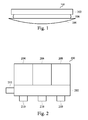
- FIG. 1 is a side view of a semiconductor wafer assembly according to an embodiment
- FIG. 2 is a block diagram of a wafer debonding and cleaning apparatus according to an embodiment
- FIG. 3A-3B are side views of a semiconductor wafer at various stages of processing according to an embodiment.
- FIG. 4 is a flow chart of a method of using the wafer debonding and clean apparatus according to an embodiment.
- FIG. 1 is a side view of a wafer assembly 100 .
- Wafer assembly 100 includes a semiconductor wafer 102 bonded to a carrier wafer 104 by an adhesive 106 .
- semiconductor wafer 102 is silicon.
- semiconductor wafer 102 is germanium, gallium arsenic, or other suitable semiconductor material.
- carrier wafer 104 is sapphire.
- carrier wafer 104 is silicon, a thermoplastic polymer, oxide, carbide, or other suitable material.
- adhesive 106 is a spin-on adhesive.
- adhesive 106 is a laminated tape, wax, or other suitable material.
- FIG. 2 is a block diagram of a wafer debonding and cleaning apparatus 200 including an automatic wafer handling module 202 for transferring/transporting semiconductor wafer 102 to/from various modules.
- Wafer debonding and cleaning apparatus 200 also includes a wafer debonding module 204 for separating semiconductor wafer 102 from carrier wafer 104 and two wafer cleaning modules 206 and 208 for removing adhesive 106 from semiconductor wafer 102 .
- Wafer debonding and cleaning apparatus further includes storage units 210 for storing multiple semiconductor wafers 102 or wafer assemblies 100 .
- a scanning module 212 scans barcodes on semiconductor wafer 102 for tracking purposes.
- wafer debonding and cleaning apparatus 200 may be integrated into a single apparatus.
- wafer debonding and cleaning apparatus may be separating into different apparatuses.
- One of ordinary skill in the art would recognize as the distance between apparatuses increases the time to transport wafer assembly 100 or semiconductor wafer 102 to/from the different apparatuses increases.
- Automatic wafer handling module 202 removes the need for manual transportation of the wafer assembly thus increasing production yield and decreased production cost.
- the automatic wafer handling module is a robotic arm.
- automatic wafer handling module 202 includes multiple robotic arms.
- the robotic arm has a blade portion configured to support the semiconductor wafer 102 or wafer assembly 100 .
- the blade portion includes sensors to enhance the positioning of the blade portion with respect to semiconductor wafer 102 or wafer assembly 100 ( FIG. 1 ) to prevent scratching a surface of semiconductor wafer 102 ( FIGS. 1 and 3A-3B ).
- the blade portion is substantially U-shaped to minimize the amount of contact between the blade portion and the wafer assembly. In other embodiments, the blade portion is circular, rectilinear or another suitable shape for supporting and moving semiconductor wafer 102 wafer assembly 100 .
- the blade portion does not need to evenly support the entire surface of the wafer assembly because semiconductor wafer 202 ( FIG. 2A-2C ) has a thickness ranging from about 350 ⁇ m to about 1500 ⁇ m. This range, in some embodiments, is narrower, e.g., from 350 ⁇ m to 1500 ⁇ m. Semiconductor wafer 102 has enhanced mechanical strength capable of withstanding the debonding and cleaning processes without significant risk of warping or fracture due to the larger thickness.
- Automatic wafer handling module 202 loads wafer assembly 100 ( FIG. 1 ), into wafer debonding module 204 . Following loading, wafer assembly 200 is transferred to a debonding stage. On the debonding stage, wafer assembly 100 is irradiated to weaken an adhesive 106 bonding semiconductor wafer 102 and carrier wafer 104 . In some embodiments, wafer assembly 100 is irradiated with ultraviolet light. In other embodiments, wafer assembly 100 is irradiated with laser light, thermal energy or other suitable types of energy to weaken the bond between carrier wafer 104 and semiconductor wafer 102 . Following irradiation, wafer assembly 100 is transferred off the debonding stage and carrier wafer 104 is lifted off semiconductor wafer 102 .
- a portion of adhesive 106 remains attached to each of semiconductor wafer 102 and carrier wafer 104 .
- Carrier wafer 104 is cleaned and stored for use with another semiconductor wafer. Following the debonding process, semiconductor wafer 102 resembles the structure shown in FIG. 3A .
- Automatic wafer handling module 202 removes semiconductor wafer 102 from wafer debonding module 204 following removal of the carrier wafer 104 . Automatic wafer handling module 202 then transfers semiconductor wafer 102 , shown in FIG. 3A , to a cleaning module 206 or 208 .
- semiconductor wafer 102 ( FIG. 3A ) is positioned on a cleaning stage.
- the cleaning stage is configured to rotate, e.g., by the use of a motor, semiconductor wafer 102 .
- a nozzle positioned above the cleaning stage supplies a solvent solution onto the surface of semiconductor wafer 102 bonded to residual adhesive 106 .
- the solvent solution is a mixture of deionized water, tetramethylammonium hydroxide (TMAH), potassium hydroxide (KOH), methylpyrrolidone (NMP), isopropanol (IPA), ethanol, acetone, hydrogen peroxide (H 2 O 2 ) and dimethyl sulfoixde (DMSO).
- TMAH tetramethylammonium hydroxide
- KOH potassium hydroxide
- NMP methylpyrrolidone
- IPA isopropanol
- ethanol acetone
- hydrogen peroxide H 2 O 2
- DMSO dimethyl sulfoixde
- cleaning module 206 or 208 further includes brushes to help remove residual adhesive 106 from semiconductor substrate 106 .
- Some embodiments of cleaning module 206 or 208 use the nozzle to spray high pressure air or liquid onto semiconductor wafer 102 to remove residual adhesive 106 .
- cleaning module 206 or 208 use the nozzle to introduce different chemicals onto semiconductor wafer 102 to chemically remove residual adhesive 106 from semiconductor wafer 102 .
- residual adhesive 106 is sufficiently removed from semiconductor wafer 102 for further processing, e.g., packing and dicing, as shown in FIG. 3B .
- Automatic wafer handling module 202 removes semiconductor wafer 102 from cleaning module 206 or 208 .
- Wafer debonding and cleaning apparatus 200 includes a second cleaning module 208 .
- the cleaning process requires more time than the wafer debonding process.
- second cleaning module 208 wafer debonding and cleaning apparatus 200 increases efficiency by eliminating a production bottleneck at the wafer cleaning process.
- Automatic wafer handling module 202 is equipped with a control system (not shown) to determine which cleaning module to use. The control system connects to cleaning modules 206 and 208 and to automatic wafer handling module 202 and determines whether either cleaning module is available to accept semiconductor wafer 102 ( FIG. 3A ).
- automatic wafer handling module 202 places a wafer assembly 100 or a semiconductor wafer 102 in one of storage units 210 when the wafer assembly 100 or the semiconductor wafer 102 is not in either debonding module 204 or cleaning modules 206 or 206 .
- Storage units 210 include support arrangements designed to support a plurality of wafer assemblies 100 or semiconductor wafers 102 . The spacing between wafer assemblies is sufficient to allow the automatic wafer handling module 202 to insert and remove wafer assemblies 200 or semiconductor wafers 102 without contacting adjacent wafer assemblies or semiconductor wafers to avoid damaging stored wafers.
- storage units 210 are stationary.
- automatic wafer handling module 202 removes wafer assembly 100 or semiconductor wafer 102 from a first storage unit and loads the wafer assembly or semiconductor wafer into a module 204 , 206 or 208 .
- automatic wafer handling module 202 places wafer assembly 100 or semiconductor wafer 102 in a second storage unit 210 different from the first storage unit 210 in order to move the wafer assemblies or semiconductor wafers further along the processing line.
- automatic wafer handling module 202 removes wafer assembly 100 from first storage unit 210 and loads the wafer assembly into wafer debonding module 204 .
- Automatic wafer handling module 202 then removes semiconductor wafer 102 from debonding module 204 and places the semiconductor wafer in a second storage unit 210 closer to cleaning module 206 or 208 .
- storage units 210 are movable, e.g., front opening unified pods (FOUPs), and transfer wafer assemblies 100 or semiconductor wafers 102 in groups from a present location to a new location.
- the new location is either adjacent a different module in wafer debonding and cleaning apparatus 200 or to another apparatus, such as a dicing or packaging apparatus.
- FOUPs front opening unified pods
- automatic wafer handling module 202 removes a wafer assembly 100 or semiconductor wafer 102 from storage unit 210 and loads the wafer assembly or the semiconductor wafer into a module 204 , 206 or 208 and returns the wafer assembly or the semiconductor wafer back to the same storage unit 210 following completion of the process in the module 204 , 206 or 208 .
- Storage unit 210 then moves the wafer to a new location.
- automatic wafer handling module 202 includes a robotic arm associated with each module 204 , 206 and 208 and storage units 210 are movable.
- Each robotic arm removes wafer assembly 100 or semiconductor wafer 102 from a storage unit 210 and loads the wafer assembly or the semiconductor wafer into the associated module 204 , 206 or 208 .
- the associated robotic arm removes wafer assembly 100 or semiconductor wafer 102 from the module 204 , 206 or 208 and stores the wafer assembly or the semiconductor wafer in the same storage unit 210 .
- Movable storage units 210 transfer wafer assemblies 100 or semiconductor wafers 102 between locations near each module 204 , 206 and 208 , to allow robotic arms associated with each module 204 , 206 or 208 to continue loading and removing wafer assemblies 100 or semiconductor wafers 102 without having to transfer the wafer assemblies or the semiconductor wafers between modules.
- Wafer debonding and cleaning apparatus 200 includes a wafer scanner 212 for scanning a barcode attached to each semiconductor wafer 102 prior to processing. Wafer scanner 212 scans the barcode upon semiconductor wafer 102 entering the wafer debonding and cleaning apparatus 200 . Wafer scanner 212 transmits the scanned barcode to a computer system to allow tracking of semiconductor wafers 102 throughout the production process. The ability to track semiconductor wafers 102 throughout the production process allows production errors to be located and corrected rapidly.
- FIG. 4 is a flow chart of a method 400 of using wafer debonding and cleaning apparatus 200 according to an embodiment.
- Method 400 begins with step 402 in which the barcode on the semiconductor wafer 102 is scanned by wafer scanner 212 .
- Step 404 is an optional step, in which automatic wafer handling module 202 places wafer assembly 100 into a storage unit 210 .
- automatic wafer handling module 202 loads wafer assembly 100 ( FIG. 1 ), into wafer debonding module 204 . If optional step 404 is included, automatic wafer handling module 202 removes wafer assembly 100 from storage unit 210 and loads wafer assembly 100 into wafer debonding module 204 . If optional step 404 is not included, automatic wafer handling module 202 transfers wafer assembly 100 directly from wafer scanner 212 to wafer debonding module 204 .
- wafer debonding module 204 debonds carrier wafer 104 from semiconductor wafer 102 .
- semiconductor wafer 102 FIG. 3A
- carrier wafer 104 is cleaned and stored for use with subsequent wafer assemblies, in step 410 .
- automatic wafer handling module 202 transfers the semiconductor wafer 102 to a storage unit 210 .
- automatic wafer handling module 202 loads the semiconductor wafer 102 ( FIG. 3A ), into wafer cleaning module 206 or 208 . If optional step 412 is included, automatic wafer handling module 202 removes semiconductor wafer 102 from storage unit 210 and loads the semiconductor wafer into wafer cleaning module 206 or 208 . If optional step 412 is not included, automatic wafer handling module 202 takes semiconductor wafer 102 directly from wafer debonding module 204 to wafer cleaning module 206 or 208 .
- the control system (not shown) connected to automatic wafer handling module 202 and wafer cleaning modules 206 and 208 determines to which wafer cleaning module 206 or 208 , semiconductor wafer 102 is transferred.
- step 416 semiconductor wafer 102 is cleaned in wafer cleaning module 206 or 208 , to produce semiconductor wafer 102 ( FIG. 3B ). Following the cleaning process, semiconductor wafer 102 is removed from wafer cleaning module 206 or 208 , in step 418 .
- step 420 semiconductor wafer 102 is sent to a packaging or dicing apparatus for further processing of the semiconductor wafer 102 .
- wafer debonding and cleaning apparatus 200 includes movable storage units 210
- semiconductor wafer 102 is placed in the storage unit 210 and storage unit 210 is transferred to the packaging or dicing apparatus.
- wafer debonding and cleaning apparatus 200 includes stationary storage units 210
- semiconductor wafer 102 is placed on a conveyor, a separate movable storage unit or some other device for transporting semiconductor wafer 102 to the dicing and/or packaging device.
- One aspect of the description relates to a wafer debonding and cleaning apparatus including an automatic wafer handling module, a wafer debonding module, and a wafer cleaning module, where the automatic wafer handling module loads a semiconductor wafer into the wafer debonding module and the wafer cleaning module.
- Another aspect of the description relates to a method of debonding and cleaning a wafer including loading a semiconductor wafer bonded to a carrier wafer into a wafer debonding module using an automatic wafer handling module, separating the semiconductor wafer from the carrier wafer, removing the semiconductor wafer from the wafer debonding module using the automatic wafer handling module, loading the semiconductor wafer into a wafer cleaning module using the automatic wafer handling module, cleaning a surface of the semiconductor wafer using the wafer cleaning module and removing the semiconductor wafer from the wafer cleaning module using the automatic wafer handling module.
Abstract
Description
Claims (20)
Priority Applications (5)
| Application Number | Priority Date | Filing Date | Title |
|---|---|---|---|
| US13/306,625 US9390949B2 (en) | 2011-11-29 | 2011-11-29 | Wafer debonding and cleaning apparatus and method of use |
| TW101112188A TWI466215B (en) | 2011-11-29 | 2012-04-06 | Methods and apparatuses of debonding and cleaning wafers |
| CN201210190020.0A CN103137524B (en) | 2011-11-29 | 2012-06-08 | Wafer separate and cleaning device and using method thereof |
| US14/479,806 US10381254B2 (en) | 2011-11-29 | 2014-09-08 | Wafer debonding and cleaning apparatus and method |
| US16/444,010 US11264262B2 (en) | 2011-11-29 | 2019-06-18 | Wafer debonding and cleaning apparatus |
Applications Claiming Priority (1)
| Application Number | Priority Date | Filing Date | Title |
|---|---|---|---|
| US13/306,625 US9390949B2 (en) | 2011-11-29 | 2011-11-29 | Wafer debonding and cleaning apparatus and method of use |
Related Child Applications (1)
| Application Number | Title | Priority Date | Filing Date |
|---|---|---|---|
| US14/479,806 Continuation-In-Part US10381254B2 (en) | 2011-11-29 | 2014-09-08 | Wafer debonding and cleaning apparatus and method |
Publications (2)
| Publication Number | Publication Date |
|---|---|
| US20130133688A1 US20130133688A1 (en) | 2013-05-30 |
| US9390949B2 true US9390949B2 (en) | 2016-07-12 |
Family
ID=48465690
Family Applications (1)
| Application Number | Title | Priority Date | Filing Date |
|---|---|---|---|
| US13/306,625 Active 2033-01-24 US9390949B2 (en) | 2011-11-29 | 2011-11-29 | Wafer debonding and cleaning apparatus and method of use |
Country Status (3)
| Country | Link |
|---|---|
| US (1) | US9390949B2 (en) |
| CN (1) | CN103137524B (en) |
| TW (1) | TWI466215B (en) |
Cited By (1)
| Publication number | Priority date | Publication date | Assignee | Title |
|---|---|---|---|---|
| US11335607B2 (en) * | 2020-07-09 | 2022-05-17 | Tokyo Electron Limited | Apparatus and methods for wafer to wafer bonding |
Families Citing this family (3)
| Publication number | Priority date | Publication date | Assignee | Title |
|---|---|---|---|---|
| CN104701214B (en) * | 2013-12-04 | 2017-11-03 | 中芯国际集成电路制造(上海)有限公司 | Semiconductor processing system |
| US9475272B2 (en) * | 2014-10-09 | 2016-10-25 | Taiwan Semiconductor Manufacturing Company, Ltd. | De-bonding and cleaning process and system |
| WO2020185745A1 (en) * | 2019-03-11 | 2020-09-17 | Versum Materials Us, Llc | Etching solution and method for aluminum nitride |
Citations (48)
| Publication number | Priority date | Publication date | Assignee | Title |
|---|---|---|---|---|
| US5391917A (en) | 1993-05-10 | 1995-02-21 | International Business Machines Corporation | Multiprocessor module packaging |
| US5510298A (en) | 1991-09-12 | 1996-04-23 | Texas Instruments Incorporated | Method of interconnect in an integrated circuit |
| US5767001A (en) | 1993-05-05 | 1998-06-16 | Siemens Aktiengesellschaft | Process for producing semiconductor components between which contact is made vertically |
| US5998292A (en) | 1997-11-12 | 1999-12-07 | International Business Machines Corporation | Method for making three dimensional circuit integration |
| US6122566A (en) * | 1998-03-03 | 2000-09-19 | Applied Materials Inc. | Method and apparatus for sequencing wafers in a multiple chamber, semiconductor wafer processing system |
| US6184060B1 (en) | 1996-10-29 | 2001-02-06 | Trusi Technologies Llc | Integrated circuits and methods for their fabrication |
| US6206441B1 (en) | 1999-08-03 | 2001-03-27 | Taiwan Semiconductor Manufacturing Company, Ltd. | Apparatus and method for transferring wafers by robot |
| US6322903B1 (en) | 1999-12-06 | 2001-11-27 | Tru-Si Technologies, Inc. | Package of integrated circuits and vertical integration |
| US6342434B1 (en) * | 1995-12-04 | 2002-01-29 | Hitachi, Ltd. | Methods of processing semiconductor wafer, and producing IC card, and carrier |
| US6448168B1 (en) | 1997-09-30 | 2002-09-10 | Intel Corporation | Method for distributing a clock on the silicon backside of an integrated circuit |
| US6465892B1 (en) | 1999-04-13 | 2002-10-15 | Oki Electric Industry Co., Ltd. | Interconnect structure for stacked semiconductor device |
| US20030008437A1 (en) | 1998-02-25 | 2003-01-09 | Seiko Epson Corporation | Method of separating thin film device, method of transferring thin film device, thin film device, active matrix substrate and liquid crystal display device |
| US6538333B2 (en) | 2000-06-16 | 2003-03-25 | Chartered Semiconductor Manufacturing Ltd. | Three dimensional IC package module |
| US6543988B2 (en) | 2001-07-18 | 2003-04-08 | Taiwan Semiconductor Manufacturing Co., Ltd | Apparatus for clamping and transporting a semiconductor wafer |
| US6599778B2 (en) | 2001-12-19 | 2003-07-29 | International Business Machines Corporation | Chip and wafer integration process using vertical connections |
| US6664129B2 (en) | 1996-10-29 | 2003-12-16 | Tri-Si Technologies, Inc. | Integrated circuits and methods for their fabrication |
| US20040089421A1 (en) * | 2002-02-15 | 2004-05-13 | Komandur Srinivasan M. | Distributed control system for semiconductor manufacturing equipment |
| US6800930B2 (en) | 2002-07-31 | 2004-10-05 | Micron Technology, Inc. | Semiconductor dice having back side redistribution layer accessed using through-silicon vias, and assemblies |
| US20040197179A1 (en) * | 2003-04-03 | 2004-10-07 | Applied Materials, Inc. | Method and apparatus for vertical transfer of semiconductor substrates between cleaning modules |
| US6841883B1 (en) | 2003-03-31 | 2005-01-11 | Micron Technology, Inc. | Multi-dice chip scale semiconductor components and wafer level methods of fabrication |
| US6924551B2 (en) | 2003-05-28 | 2005-08-02 | Intel Corporation | Through silicon via, folded flex microelectronic package |
| US20050233547A1 (en) * | 2002-06-03 | 2005-10-20 | Kazuki Noda | Laminate body, method, and apparatus for manufacturing ultrathin substrate using the laminate body |
| US6962872B2 (en) | 2002-12-09 | 2005-11-08 | International Business Machines Corporation | High density chip carrier with integrated passive devices |
| US7049170B2 (en) | 2003-12-17 | 2006-05-23 | Tru-Si Technologies, Inc. | Integrated circuits and packaging substrates with cavities, and attachment methods including insertion of protruding contact pads into cavities |
| US7060601B2 (en) | 2003-12-17 | 2006-06-13 | Tru-Si Technologies, Inc. | Packaging substrates for integrated circuits and soldering methods |
| US7071546B2 (en) | 2002-01-16 | 2006-07-04 | Alfred E. Mann Foundation For Scientific Research | Space-saving packaging of electronic circuits |
| US7100826B1 (en) * | 2001-03-26 | 2006-09-05 | Advanced Micro Devices, Inc. | Barcode marking of wafer products for inventory control |
| US7111149B2 (en) | 2003-07-07 | 2006-09-19 | Intel Corporation | Method and apparatus for generating a device ID for stacked devices |
| US7122912B2 (en) | 2004-01-28 | 2006-10-17 | Nec Electronics Corporation | Chip and multi-chip semiconductor device using thereof and method for manufacturing same |
| US7157787B2 (en) | 2002-02-20 | 2007-01-02 | Intel Corporation | Process of vertically stacking multiple wafers supporting different active integrated circuit (IC) devices |
| US7193308B2 (en) | 2003-09-26 | 2007-03-20 | Seiko Epson Corporation | Intermediate chip module, semiconductor device, circuit board, and electronic device |
| US7262495B2 (en) | 2004-10-07 | 2007-08-28 | Hewlett-Packard Development Company, L.P. | 3D interconnect with protruding contacts |
| US7297574B2 (en) | 2005-06-17 | 2007-11-20 | Infineon Technologies Ag | Multi-chip device and method for producing a multi-chip device |
| US7335972B2 (en) | 2003-11-13 | 2008-02-26 | Sandia Corporation | Heterogeneously integrated microsystem-on-a-chip |
| US7364922B2 (en) * | 2005-01-24 | 2008-04-29 | Tokyo Electron Limited | Automated semiconductor wafer salvage during processing |
| US20080099149A1 (en) | 2005-10-04 | 2008-05-01 | International Business Machines Corporation | Rework process for removing residual uv adhesive from c4 wafer surfaces |
| US20090075217A1 (en) | 2007-09-19 | 2009-03-19 | International Business Machines Corporation | Tapered edge bead removal process for immersion lithography |
| US20090314438A1 (en) * | 2008-06-18 | 2009-12-24 | Tokyo Ohka Kogyo Co., Ltd. | Supporting plate peeling apparatus |
| US20100148353A1 (en) | 2008-12-11 | 2010-06-17 | Stats Chippac, Ltd. | Double-Sided Semiconductor Device and Method of Forming Top-Side and Bottom-Side Interconnect Structures |
| US20100263794A1 (en) | 2009-04-16 | 2010-10-21 | Suss Microtec Inc | Apparatus for mechanically debonding temporary bonded semiconductor wafers |
| TW201039298A (en) | 2009-04-17 | 2010-11-01 | Ind Tech Res Inst | Method for isolating a flexible film from a substrate and method for fabricating an electric device |
| TW201039297A (en) | 2009-04-17 | 2010-11-01 | Ind Tech Res Inst | Method for isolating a flexible substrate from a carrier and method for fabricating an electric device |
| US20100330788A1 (en) | 2009-06-30 | 2010-12-30 | Taiwan Semiconductor Manufacturing Company, Ltd. | Thin wafer handling structure and method |
| US20110041764A1 (en) * | 2006-06-26 | 2011-02-24 | Aaron Webb | Batch processing platform for ald and cvd |
| US7935780B2 (en) * | 2007-06-25 | 2011-05-03 | Brewer Science Inc. | High-temperature spin-on temporary bonding compositions |
| US20110146901A1 (en) * | 2009-12-23 | 2011-06-23 | Suss Microtec Inc | Automated thermal slide debonder |
| US20120080150A1 (en) * | 2010-10-05 | 2012-04-05 | Skyworks Solutions, Inc. | Fixtures and methods for unbonding wafers by shear force |
| JP2014053465A (en) | 2012-09-07 | 2014-03-20 | Tokyo Electron Ltd | Peeling system |
Family Cites Families (3)
| Publication number | Priority date | Publication date | Assignee | Title |
|---|---|---|---|---|
| US6491083B2 (en) * | 2001-02-06 | 2002-12-10 | Anadigics, Inc. | Wafer demount receptacle for separation of thinned wafer from mounting carrier |
| US6736929B2 (en) * | 2002-02-15 | 2004-05-18 | Nutool, Inc. | Distributed control system for semiconductor manufacturing equipment |
| JP4668833B2 (en) * | 2006-04-26 | 2011-04-13 | 三菱電機株式会社 | Semiconductor wafer separation apparatus and separation method |
-
2011
- 2011-11-29 US US13/306,625 patent/US9390949B2/en active Active
-
2012
- 2012-04-06 TW TW101112188A patent/TWI466215B/en active
- 2012-06-08 CN CN201210190020.0A patent/CN103137524B/en active Active
Patent Citations (56)
| Publication number | Priority date | Publication date | Assignee | Title |
|---|---|---|---|---|
| US5510298A (en) | 1991-09-12 | 1996-04-23 | Texas Instruments Incorporated | Method of interconnect in an integrated circuit |
| US5767001A (en) | 1993-05-05 | 1998-06-16 | Siemens Aktiengesellschaft | Process for producing semiconductor components between which contact is made vertically |
| US5391917A (en) | 1993-05-10 | 1995-02-21 | International Business Machines Corporation | Multiprocessor module packaging |
| US6342434B1 (en) * | 1995-12-04 | 2002-01-29 | Hitachi, Ltd. | Methods of processing semiconductor wafer, and producing IC card, and carrier |
| US6639303B2 (en) | 1996-10-29 | 2003-10-28 | Tru-Si Technolgies, Inc. | Integrated circuits and methods for their fabrication |
| US6740582B2 (en) | 1996-10-29 | 2004-05-25 | Tru-Si Technologies, Inc. | Integrated circuits and methods for their fabrication |
| US6184060B1 (en) | 1996-10-29 | 2001-02-06 | Trusi Technologies Llc | Integrated circuits and methods for their fabrication |
| US6882030B2 (en) | 1996-10-29 | 2005-04-19 | Tru-Si Technologies, Inc. | Integrated circuit structures with a conductor formed in a through hole in a semiconductor substrate and protruding from a surface of the substrate |
| US6664129B2 (en) | 1996-10-29 | 2003-12-16 | Tri-Si Technologies, Inc. | Integrated circuits and methods for their fabrication |
| US6448168B1 (en) | 1997-09-30 | 2002-09-10 | Intel Corporation | Method for distributing a clock on the silicon backside of an integrated circuit |
| US5998292A (en) | 1997-11-12 | 1999-12-07 | International Business Machines Corporation | Method for making three dimensional circuit integration |
| US20030008437A1 (en) | 1998-02-25 | 2003-01-09 | Seiko Epson Corporation | Method of separating thin film device, method of transferring thin film device, thin film device, active matrix substrate and liquid crystal display device |
| US6122566A (en) * | 1998-03-03 | 2000-09-19 | Applied Materials Inc. | Method and apparatus for sequencing wafers in a multiple chamber, semiconductor wafer processing system |
| US6465892B1 (en) | 1999-04-13 | 2002-10-15 | Oki Electric Industry Co., Ltd. | Interconnect structure for stacked semiconductor device |
| US6472293B2 (en) | 1999-04-13 | 2002-10-29 | Oki Electric Industry Co., Ltd. | Method for manufacturing an interconnect structure for stacked semiconductor device |
| US6206441B1 (en) | 1999-08-03 | 2001-03-27 | Taiwan Semiconductor Manufacturing Company, Ltd. | Apparatus and method for transferring wafers by robot |
| US6322903B1 (en) | 1999-12-06 | 2001-11-27 | Tru-Si Technologies, Inc. | Package of integrated circuits and vertical integration |
| US6693361B1 (en) | 1999-12-06 | 2004-02-17 | Tru-Si Technologies, Inc. | Packaging of integrated circuits and vertical integration |
| US6538333B2 (en) | 2000-06-16 | 2003-03-25 | Chartered Semiconductor Manufacturing Ltd. | Three dimensional IC package module |
| US7100826B1 (en) * | 2001-03-26 | 2006-09-05 | Advanced Micro Devices, Inc. | Barcode marking of wafer products for inventory control |
| US6543988B2 (en) | 2001-07-18 | 2003-04-08 | Taiwan Semiconductor Manufacturing Co., Ltd | Apparatus for clamping and transporting a semiconductor wafer |
| US6599778B2 (en) | 2001-12-19 | 2003-07-29 | International Business Machines Corporation | Chip and wafer integration process using vertical connections |
| US7071546B2 (en) | 2002-01-16 | 2006-07-04 | Alfred E. Mann Foundation For Scientific Research | Space-saving packaging of electronic circuits |
| US20040089421A1 (en) * | 2002-02-15 | 2004-05-13 | Komandur Srinivasan M. | Distributed control system for semiconductor manufacturing equipment |
| US7157787B2 (en) | 2002-02-20 | 2007-01-02 | Intel Corporation | Process of vertically stacking multiple wafers supporting different active integrated circuit (IC) devices |
| US20050233547A1 (en) * | 2002-06-03 | 2005-10-20 | Kazuki Noda | Laminate body, method, and apparatus for manufacturing ultrathin substrate using the laminate body |
| US6800930B2 (en) | 2002-07-31 | 2004-10-05 | Micron Technology, Inc. | Semiconductor dice having back side redistribution layer accessed using through-silicon vias, and assemblies |
| US7355273B2 (en) | 2002-07-31 | 2008-04-08 | Micron Technology, Inc. | Semiconductor dice having back side redistribution layer accessed using through-silicon vias, methods |
| US6962867B2 (en) | 2002-07-31 | 2005-11-08 | Microntechnology, Inc. | Methods of fabrication of semiconductor dice having back side redistribution layer accessed using through-silicon vias and assemblies thereof |
| US6962872B2 (en) | 2002-12-09 | 2005-11-08 | International Business Machines Corporation | High density chip carrier with integrated passive devices |
| US7030481B2 (en) | 2002-12-09 | 2006-04-18 | Internation Business Machines Corporation | High density chip carrier with integrated passive devices |
| US6841883B1 (en) | 2003-03-31 | 2005-01-11 | Micron Technology, Inc. | Multi-dice chip scale semiconductor components and wafer level methods of fabrication |
| US20040197179A1 (en) * | 2003-04-03 | 2004-10-07 | Applied Materials, Inc. | Method and apparatus for vertical transfer of semiconductor substrates between cleaning modules |
| US6924551B2 (en) | 2003-05-28 | 2005-08-02 | Intel Corporation | Through silicon via, folded flex microelectronic package |
| US7111149B2 (en) | 2003-07-07 | 2006-09-19 | Intel Corporation | Method and apparatus for generating a device ID for stacked devices |
| US7193308B2 (en) | 2003-09-26 | 2007-03-20 | Seiko Epson Corporation | Intermediate chip module, semiconductor device, circuit board, and electronic device |
| US7335972B2 (en) | 2003-11-13 | 2008-02-26 | Sandia Corporation | Heterogeneously integrated microsystem-on-a-chip |
| US7060601B2 (en) | 2003-12-17 | 2006-06-13 | Tru-Si Technologies, Inc. | Packaging substrates for integrated circuits and soldering methods |
| US7049170B2 (en) | 2003-12-17 | 2006-05-23 | Tru-Si Technologies, Inc. | Integrated circuits and packaging substrates with cavities, and attachment methods including insertion of protruding contact pads into cavities |
| US7122912B2 (en) | 2004-01-28 | 2006-10-17 | Nec Electronics Corporation | Chip and multi-chip semiconductor device using thereof and method for manufacturing same |
| US7262495B2 (en) | 2004-10-07 | 2007-08-28 | Hewlett-Packard Development Company, L.P. | 3D interconnect with protruding contacts |
| US7364922B2 (en) * | 2005-01-24 | 2008-04-29 | Tokyo Electron Limited | Automated semiconductor wafer salvage during processing |
| US7297574B2 (en) | 2005-06-17 | 2007-11-20 | Infineon Technologies Ag | Multi-chip device and method for producing a multi-chip device |
| US20080099149A1 (en) | 2005-10-04 | 2008-05-01 | International Business Machines Corporation | Rework process for removing residual uv adhesive from c4 wafer surfaces |
| US20110041764A1 (en) * | 2006-06-26 | 2011-02-24 | Aaron Webb | Batch processing platform for ald and cvd |
| US7935780B2 (en) * | 2007-06-25 | 2011-05-03 | Brewer Science Inc. | High-temperature spin-on temporary bonding compositions |
| US20090075217A1 (en) | 2007-09-19 | 2009-03-19 | International Business Machines Corporation | Tapered edge bead removal process for immersion lithography |
| US20090314438A1 (en) * | 2008-06-18 | 2009-12-24 | Tokyo Ohka Kogyo Co., Ltd. | Supporting plate peeling apparatus |
| US20100148353A1 (en) | 2008-12-11 | 2010-06-17 | Stats Chippac, Ltd. | Double-Sided Semiconductor Device and Method of Forming Top-Side and Bottom-Side Interconnect Structures |
| US20100263794A1 (en) | 2009-04-16 | 2010-10-21 | Suss Microtec Inc | Apparatus for mechanically debonding temporary bonded semiconductor wafers |
| TW201039298A (en) | 2009-04-17 | 2010-11-01 | Ind Tech Res Inst | Method for isolating a flexible film from a substrate and method for fabricating an electric device |
| TW201039297A (en) | 2009-04-17 | 2010-11-01 | Ind Tech Res Inst | Method for isolating a flexible substrate from a carrier and method for fabricating an electric device |
| US20100330788A1 (en) | 2009-06-30 | 2010-12-30 | Taiwan Semiconductor Manufacturing Company, Ltd. | Thin wafer handling structure and method |
| US20110146901A1 (en) * | 2009-12-23 | 2011-06-23 | Suss Microtec Inc | Automated thermal slide debonder |
| US20120080150A1 (en) * | 2010-10-05 | 2012-04-05 | Skyworks Solutions, Inc. | Fixtures and methods for unbonding wafers by shear force |
| JP2014053465A (en) | 2012-09-07 | 2014-03-20 | Tokyo Electron Ltd | Peeling system |
Non-Patent Citations (3)
| Title |
|---|
| Brewer Science WaferBOND HT-10.10 Temporary Wafer Bonding Material brochure; Aug. 9, 2011. * |
| Office Action dated Apr. 22, 2016 and English translation from corresponding No. KR 102015-0097254. |
| Office Action dated Feb. 20, 2014 from corresponding application No. TW 101112188. |
Cited By (1)
| Publication number | Priority date | Publication date | Assignee | Title |
|---|---|---|---|---|
| US11335607B2 (en) * | 2020-07-09 | 2022-05-17 | Tokyo Electron Limited | Apparatus and methods for wafer to wafer bonding |
Also Published As
| Publication number | Publication date |
|---|---|
| US20130133688A1 (en) | 2013-05-30 |
| TW201322354A (en) | 2013-06-01 |
| TWI466215B (en) | 2014-12-21 |
| CN103137524A (en) | 2013-06-05 |
| CN103137524B (en) | 2016-06-01 |
Similar Documents
| Publication | Publication Date | Title |
|---|---|---|
| KR101823718B1 (en) | Substrate inverting device, substrate inverting method, and peeling system | |
| KR101922262B1 (en) | Peeling apparatus, peeling system and peeling method | |
| KR101900113B1 (en) | Peeling apparatus, peeling system and peeling method | |
| US10381254B2 (en) | Wafer debonding and cleaning apparatus and method | |
| JP5580806B2 (en) | Peeling apparatus, peeling system, peeling method, program, and computer storage medium | |
| TWI533366B (en) | Adhesive tape joining method and adhesive tape joining apparatus | |
| WO2013136982A1 (en) | Peeling apparatus, peeling system, and peeling method | |
| JP6158721B2 (en) | Cleaning device, peeling system, cleaning method, program, and computer storage medium | |
| TW201423832A (en) | Separation device, separation system, and separation method | |
| US9390949B2 (en) | Wafer debonding and cleaning apparatus and method of use | |
| KR101847661B1 (en) | Delamination system | |
| TWI745532B (en) | Semiconductor substrate treatment method and treatment device | |
| KR101837227B1 (en) | Release device, release system, release method, and computer storage medium | |
| KR101805964B1 (en) | Peeling system, peeling method, and computer storage medium | |
| KR101999054B1 (en) | Wafer debonding and cleaning apparatus and method | |
| US11264262B2 (en) | Wafer debonding and cleaning apparatus | |
| JP2015088620A (en) | Peeling system, peeling method, program, and computer storage medium | |
| JP2013106026A (en) | Separation device and method of semiconductor wafer | |
| JP2005276987A (en) | Ultra-thin chip manufacturing process and manufacturing apparatus therefor | |
| JP6466217B2 (en) | Peeling device and peeling system | |
| WO2023145558A1 (en) | Substrate-processing device and substrate-processing method | |
| WO2023100831A1 (en) | Chip periphery peeling apparatus, chip supply apparatus, chip supply system, chip bonding system, pickup apparatus, chip periphery peeling method, chip supply method, chip bonding method, and pickup method | |
| WO2023144971A1 (en) | Substrate processing apparatus and substrate processing method | |
| JP2017183413A (en) | Substrate transfer method and substrate transfer device | |
| JP5808721B2 (en) | Peeling system |
Legal Events
| Date | Code | Title | Description |
|---|---|---|---|
| AS | Assignment |
Owner name: TAIWAN SEMICONDUCTOR MANUFACTURING COMPANY, LTD., Free format text: ASSIGNMENT OF ASSIGNORS INTEREST;ASSIGNORS:CHIOU, WEN-CHIH;LIN, YU-LIANG;TU, HUNG-JUNG;REEL/FRAME:027594/0009 Effective date: 20120103 |
|
| STCF | Information on status: patent grant |
Free format text: PATENTED CASE |
|
| MAFP | Maintenance fee payment |
Free format text: PAYMENT OF MAINTENANCE FEE, 4TH YEAR, LARGE ENTITY (ORIGINAL EVENT CODE: M1551); ENTITY STATUS OF PATENT OWNER: LARGE ENTITY Year of fee payment: 4 |
|
| MAFP | Maintenance fee payment |
Free format text: PAYMENT OF MAINTENANCE FEE, 8TH YEAR, LARGE ENTITY (ORIGINAL EVENT CODE: M1552); ENTITY STATUS OF PATENT OWNER: LARGE ENTITY Year of fee payment: 8 |