US9385253B2 - Method of manufacturing solar cell module - Google Patents
Method of manufacturing solar cell module Download PDFInfo
- Publication number
- US9385253B2 US9385253B2 US14/045,059 US201314045059A US9385253B2 US 9385253 B2 US9385253 B2 US 9385253B2 US 201314045059 A US201314045059 A US 201314045059A US 9385253 B2 US9385253 B2 US 9385253B2
- Authority
- US
- United States
- Prior art keywords
- silicone gel
- solar cell
- receiving panel
- sheet
- gel sheet
- Prior art date
- Legal status (The legal status is an assumption and is not a legal conclusion. Google has not performed a legal analysis and makes no representation as to the accuracy of the status listed.)
- Active, expires
Links
- 238000004519 manufacturing process Methods 0.000 title claims abstract description 32
- 229920001296 polysiloxane Polymers 0.000 claims abstract description 140
- 229920005549 butyl rubber Polymers 0.000 claims abstract description 24
- 230000002093 peripheral effect Effects 0.000 claims abstract description 12
- 238000003825 pressing Methods 0.000 claims abstract description 6
- 239000000203 mixture Substances 0.000 claims description 37
- 125000003342 alkenyl group Chemical group 0.000 claims description 30
- BASFCYQUMIYNBI-UHFFFAOYSA-N platinum Chemical compound [Pt] BASFCYQUMIYNBI-UHFFFAOYSA-N 0.000 claims description 19
- 125000004435 hydrogen atom Chemical group [H]* 0.000 claims description 15
- 229920006136 organohydrogenpolysiloxane Polymers 0.000 claims description 14
- 230000035515 penetration Effects 0.000 claims description 14
- 125000001183 hydrocarbyl group Chemical group 0.000 claims description 11
- 125000001931 aliphatic group Chemical group 0.000 claims description 10
- 239000003054 catalyst Substances 0.000 claims description 7
- 229910052697 platinum Inorganic materials 0.000 claims description 7
- 239000000463 material Substances 0.000 description 39
- -1 solar cells Substances 0.000 description 37
- 229920001577 copolymer Polymers 0.000 description 31
- 229920000139 polyethylene terephthalate Polymers 0.000 description 25
- 239000005020 polyethylene terephthalate Substances 0.000 description 25
- 238000000034 method Methods 0.000 description 23
- 238000011156 evaluation Methods 0.000 description 19
- 238000012360 testing method Methods 0.000 description 18
- 230000006866 deterioration Effects 0.000 description 15
- 125000004432 carbon atom Chemical group C* 0.000 description 14
- 239000007788 liquid Substances 0.000 description 14
- 239000000047 product Substances 0.000 description 14
- 239000004205 dimethyl polysiloxane Substances 0.000 description 11
- 235000013870 dimethyl polysiloxane Nutrition 0.000 description 11
- 229920000435 poly(dimethylsiloxane) Polymers 0.000 description 11
- 239000008393 encapsulating agent Substances 0.000 description 10
- 239000005038 ethylene vinyl acetate Substances 0.000 description 10
- 125000002496 methyl group Chemical group [H]C([H])([H])* 0.000 description 10
- 229920001200 poly(ethylene-vinyl acetate) Polymers 0.000 description 10
- 230000001681 protective effect Effects 0.000 description 10
- 238000001723 curing Methods 0.000 description 8
- 238000005538 encapsulation Methods 0.000 description 8
- 239000011521 glass Substances 0.000 description 8
- 125000001997 phenyl group Chemical group [H]C1=C([H])C([H])=C(*)C([H])=C1[H] 0.000 description 7
- 230000000052 comparative effect Effects 0.000 description 6
- 238000010438 heat treatment Methods 0.000 description 5
- 229920005989 resin Polymers 0.000 description 5
- 239000011347 resin Substances 0.000 description 5
- 239000000758 substrate Substances 0.000 description 5
- 125000000391 vinyl group Chemical group [H]C([*])=C([H])[H] 0.000 description 5
- XUIMIQQOPSSXEZ-UHFFFAOYSA-N Silicon Chemical group [Si] XUIMIQQOPSSXEZ-UHFFFAOYSA-N 0.000 description 4
- 239000011248 coating agent Substances 0.000 description 4
- 238000000576 coating method Methods 0.000 description 4
- 229920001843 polymethylhydrosiloxane Polymers 0.000 description 4
- 229910020485 SiO4/2 Inorganic materials 0.000 description 3
- VYPSYNLAJGMNEJ-UHFFFAOYSA-N Silicium dioxide Chemical group O=[Si]=O VYPSYNLAJGMNEJ-UHFFFAOYSA-N 0.000 description 3
- 239000002253 acid Substances 0.000 description 3
- 125000000217 alkyl group Chemical group 0.000 description 3
- 125000003118 aryl group Chemical group 0.000 description 3
- 230000015572 biosynthetic process Effects 0.000 description 3
- 229920000840 ethylene tetrafluoroethylene copolymer Polymers 0.000 description 3
- 239000012943 hotmelt Substances 0.000 description 3
- 239000010410 layer Substances 0.000 description 3
- 230000007774 longterm Effects 0.000 description 3
- 229920002620 polyvinyl fluoride Polymers 0.000 description 3
- 230000002441 reversible effect Effects 0.000 description 3
- 238000003786 synthesis reaction Methods 0.000 description 3
- 229920003002 synthetic resin Polymers 0.000 description 3
- 239000000057 synthetic resin Substances 0.000 description 3
- 238000011179 visual inspection Methods 0.000 description 3
- 125000003903 2-propenyl group Chemical group [H]C([*])([H])C([H])=C([H])[H] 0.000 description 2
- 229920000178 Acrylic resin Polymers 0.000 description 2
- 239000004925 Acrylic resin Substances 0.000 description 2
- WKBOTKDWSSQWDR-UHFFFAOYSA-N Bromine atom Chemical compound [Br] WKBOTKDWSSQWDR-UHFFFAOYSA-N 0.000 description 2
- ZAMOUSCENKQFHK-UHFFFAOYSA-N Chlorine atom Chemical compound [Cl] ZAMOUSCENKQFHK-UHFFFAOYSA-N 0.000 description 2
- PXGOKWXKJXAPGV-UHFFFAOYSA-N Fluorine Chemical compound FF PXGOKWXKJXAPGV-UHFFFAOYSA-N 0.000 description 2
- XEEYBQQBJWHFJM-UHFFFAOYSA-N Iron Chemical compound [Fe] XEEYBQQBJWHFJM-UHFFFAOYSA-N 0.000 description 2
- 239000004743 Polypropylene Substances 0.000 description 2
- 229910020388 SiO1/2 Inorganic materials 0.000 description 2
- 229910020487 SiO3/2 Inorganic materials 0.000 description 2
- 229910052782 aluminium Inorganic materials 0.000 description 2
- XAGFODPZIPBFFR-UHFFFAOYSA-N aluminium Chemical compound [Al] XAGFODPZIPBFFR-UHFFFAOYSA-N 0.000 description 2
- 125000003710 aryl alkyl group Chemical group 0.000 description 2
- 125000001797 benzyl group Chemical group [H]C1=C([H])C([H])=C(C([H])=C1[H])C([H])([H])* 0.000 description 2
- 230000000740 bleeding effect Effects 0.000 description 2
- GDTBXPJZTBHREO-UHFFFAOYSA-N bromine Substances BrBr GDTBXPJZTBHREO-UHFFFAOYSA-N 0.000 description 2
- 229910052794 bromium Inorganic materials 0.000 description 2
- 125000004369 butenyl group Chemical group C(=CCC)* 0.000 description 2
- 125000000484 butyl group Chemical group [H]C([*])([H])C([H])([H])C([H])([H])C([H])([H])[H] 0.000 description 2
- 229910052801 chlorine Inorganic materials 0.000 description 2
- 239000000460 chlorine Substances 0.000 description 2
- 239000002131 composite material Substances 0.000 description 2
- 230000007797 corrosion Effects 0.000 description 2
- 238000005260 corrosion Methods 0.000 description 2
- 125000000113 cyclohexyl group Chemical group [H]C1([H])C([H])([H])C([H])([H])C([H])(*)C([H])([H])C1([H])[H] 0.000 description 2
- 125000002704 decyl group Chemical group [H]C([H])([H])C([H])([H])C([H])([H])C([H])([H])C([H])([H])C([H])([H])C([H])([H])C([H])([H])C([H])([H])C([H])([H])* 0.000 description 2
- 229920001971 elastomer Polymers 0.000 description 2
- 125000001495 ethyl group Chemical group [H]C([H])([H])C([H])([H])* 0.000 description 2
- 239000004744 fabric Substances 0.000 description 2
- 239000005357 flat glass Substances 0.000 description 2
- 229910052731 fluorine Inorganic materials 0.000 description 2
- 239000011737 fluorine Substances 0.000 description 2
- 125000005843 halogen group Chemical group 0.000 description 2
- 125000004051 hexyl group Chemical group [H]C([H])([H])C([H])([H])C([H])([H])C([H])([H])C([H])([H])C([H])([H])* 0.000 description 2
- 125000000959 isobutyl group Chemical group [H]C([H])([H])C([H])(C([H])([H])[H])C([H])([H])* 0.000 description 2
- 125000000555 isopropenyl group Chemical group [H]\C([H])=C(\*)C([H])([H])[H] 0.000 description 2
- 125000001449 isopropyl group Chemical group [H]C([H])([H])C([H])(*)C([H])([H])[H] 0.000 description 2
- 239000007769 metal material Substances 0.000 description 2
- 238000002156 mixing Methods 0.000 description 2
- 229910021421 monocrystalline silicon Inorganic materials 0.000 description 2
- 125000002347 octyl group Chemical group [H]C([*])([H])C([H])([H])C([H])([H])C([H])([H])C([H])([H])C([H])([H])C([H])([H])C([H])([H])[H] 0.000 description 2
- 239000003921 oil Substances 0.000 description 2
- 125000001147 pentyl group Chemical group C(CCCC)* 0.000 description 2
- 125000000286 phenylethyl group Chemical group [H]C1=C([H])C([H])=C(C([H])=C1[H])C([H])([H])C([H])([H])* 0.000 description 2
- 229920001155 polypropylene Polymers 0.000 description 2
- 125000004368 propenyl group Chemical group C(=CC)* 0.000 description 2
- 125000001436 propyl group Chemical group [H]C([*])([H])C([H])([H])C([H])([H])[H] 0.000 description 2
- 239000004065 semiconductor Substances 0.000 description 2
- 229910052710 silicon Inorganic materials 0.000 description 2
- 125000000999 tert-butyl group Chemical group [H]C([H])([H])C(*)(C([H])([H])[H])C([H])([H])[H] 0.000 description 2
- 125000003944 tolyl group Chemical group 0.000 description 2
- 229920002554 vinyl polymer Polymers 0.000 description 2
- XLYOFNOQVPJJNP-UHFFFAOYSA-N water Substances O XLYOFNOQVPJJNP-UHFFFAOYSA-N 0.000 description 2
- 229920002799 BoPET Polymers 0.000 description 1
- 241000283690 Bos taurus Species 0.000 description 1
- KQWXWNGVCAMIGQ-UHFFFAOYSA-N C[Si](C)(C)O[Si](C)(C)O[Si](C)(C)O[Si](C)(C)O[Si](C)(C)O[Si](C)(C)O[Si](C)(C)O[Si](C)(C)O[Si](C)(C)O[Si](C)(C)O[Si](C)(C)O[Si](C)(C)O[Si](C)(C)O[Si](C)(C)O[Si](C)(C)O[Si](C)(C)O[Si](C)(C)O[Si](C)(C)O[Si](C)(C)O[Si](C)(C)O[Si](C)(C)O[Si](C)(C)O[Si](C)(C)O[Si](C)(C)O[Si](C)(C)O[Si](C)(C)O[Si](C)(C)O[Si](C)(C)O[Si](C)(C)O[Si](C)(C)O[Si](C)(C)O[Si](C)(C)O[Si](C)(C)O[Si](C)(C)O[Si](C)(C)O[Si](C)(C)O[Si](C)(C)O[Si](C)(C)O[Si](C)(C)O[Si](C)(C)O[Si](C)(C)O[Si](C)(C)O[Si](C)(C)O[Si](C)(C)O[Si](C)(C)O[Si](C)(C)O[Si](C)(C)O[Si](C)(C)O[Si](C)(C)O[Si](C)(C)O[Si](C)(C)O[Si](C)(C)O[Si](C)(C)O[Si](C)(C)O[Si](C)(C)O[Si](C)(C)O[Si](C)(C)O[Si](C)(C)O[Si](C)(C)O[Si](C)(C)O[Si](C)(C)O[Si](C)(C)O[Si](C)(C)O[Si](C)(C)O[Si](C)(C)O[Si](C)(C)O[Si](C)(C)O[Si](C)(C)O[Si](C)(C)O[Si](C)(C)O[Si](C)(C)O[Si](C)(C)O[Si](C)(C)O[Si](C)(C)O[Si](C)(C)O[Si](C)(C)O[Si](C)(C)O[Si](C)(C)O[Si](C)(C)O[Si](C)(C)O[Si](C)(C)O[Si](C)(C)O[Si](C)(C)O[Si](C)(C)O[Si](C)(C)O[Si](C)(C)O[Si](C)(C)O[Si](C)(C)O[Si](C)(C)O[Si](C)(C)O[Si](C)(C)O[Si](C)(C)O[Si](C)(C)O[Si](C)(C)O[Si](C)(C)O[Si](C)(C)O[Si](C)(C)O[Si](C)(C)O[Si](C)(C)O[Si](C)(C)O[Si](C)(C)O[Si](C)(C)O[Si](C)(C)O[Si](C)(C)O[Si](C)(C)O[Si](C)(C)O[Si](C)(C)O[Si](C)(C)O[Si](C)(C)O[Si](C)(C)O[Si](C)(C)O[Si](C)(C)O[Si](C)(C)O[Si](C)(C)O[Si](C)(C)O[Si](C)(C)O[Si](C)(C)O[Si](C)(C)O[Si](C)(C)O[Si](C)(C)O[Si](C)(C)O[Si](C)(C)O[Si](C)(C)O[Si](C)(C)O[Si](C)(C)O[Si](C)(C)O[Si](C)(C)O[Si](C)(C)O[Si](C)(C)O[Si](C)(C)O[Si](C)(C)O[Si](C)(C)O[Si](C)(C)O[Si](C)(C)O[Si](C)(C)O[Si](C)(C)O[Si](C)(C)O[Si](C)(C)O[Si](C)(C)O[Si](C)(C)O[Si](C)(C)O[Si](C)(C)O[Si](C)(C)O[Si](C)(C)O[Si](C)(C)O[Si](C)(C)O[Si](C)(C)O[Si](C)(C)O[Si](C)(C)O[Si](C)(C)O[Si](C)(C)O[Si](C)(C)O[Si](C)(C)O[Si](C)(C)O[Si](C)(C)O[Si](C)(C)O[Si](C)(C)O[Si](C)(C)O[Si](C)(C)O[Si](C)(C)O[Si](C)(C)O[Si](C)(C)O[Si](C)(C)O[Si](C)(C)O[Si](C)(C)O[Si](C)(C)O[Si](C)(C)O[Si](C)(C)O[Si](C)(C)O[Si](C)(C)O[Si](C)(C)O[Si](C)(C)O[Si](C)(C)O[Si](C)(C)O[Si](C)(C)O[Si](C)(C)O[Si](C)(C)O[Si](C)(C)O[Si](C)(C)O[Si](C)(C)O[Si](C)(C)O[Si](C)(C)O[Si](C)(C)O[Si](C)(C)O[Si](C)(C)O[Si](C)(C)O[Si](C)(C)O[Si](C)(C)O[Si](C)(C)O[Si](C)(C)O[Si](C)(C)O[Si](C)(C)O[Si](C)(C)O[Si](C)(C)O[Si](C)(C)O[Si](C)(C)O[Si](C)(C)O[Si](C)(C)O[Si](C)(C)O[Si](C)(C)O[Si](C)(C)O[Si](C)(C)C Chemical compound C[Si](C)(C)O[Si](C)(C)O[Si](C)(C)O[Si](C)(C)O[Si](C)(C)O[Si](C)(C)O[Si](C)(C)O[Si](C)(C)O[Si](C)(C)O[Si](C)(C)O[Si](C)(C)O[Si](C)(C)O[Si](C)(C)O[Si](C)(C)O[Si](C)(C)O[Si](C)(C)O[Si](C)(C)O[Si](C)(C)O[Si](C)(C)O[Si](C)(C)O[Si](C)(C)O[Si](C)(C)O[Si](C)(C)O[Si](C)(C)O[Si](C)(C)O[Si](C)(C)O[Si](C)(C)O[Si](C)(C)O[Si](C)(C)O[Si](C)(C)O[Si](C)(C)O[Si](C)(C)O[Si](C)(C)O[Si](C)(C)O[Si](C)(C)O[Si](C)(C)O[Si](C)(C)O[Si](C)(C)O[Si](C)(C)O[Si](C)(C)O[Si](C)(C)O[Si](C)(C)O[Si](C)(C)O[Si](C)(C)O[Si](C)(C)O[Si](C)(C)O[Si](C)(C)O[Si](C)(C)O[Si](C)(C)O[Si](C)(C)O[Si](C)(C)O[Si](C)(C)O[Si](C)(C)O[Si](C)(C)O[Si](C)(C)O[Si](C)(C)O[Si](C)(C)O[Si](C)(C)O[Si](C)(C)O[Si](C)(C)O[Si](C)(C)O[Si](C)(C)O[Si](C)(C)O[Si](C)(C)O[Si](C)(C)O[Si](C)(C)O[Si](C)(C)O[Si](C)(C)O[Si](C)(C)O[Si](C)(C)O[Si](C)(C)O[Si](C)(C)O[Si](C)(C)O[Si](C)(C)O[Si](C)(C)O[Si](C)(C)O[Si](C)(C)O[Si](C)(C)O[Si](C)(C)O[Si](C)(C)O[Si](C)(C)O[Si](C)(C)O[Si](C)(C)O[Si](C)(C)O[Si](C)(C)O[Si](C)(C)O[Si](C)(C)O[Si](C)(C)O[Si](C)(C)O[Si](C)(C)O[Si](C)(C)O[Si](C)(C)O[Si](C)(C)O[Si](C)(C)O[Si](C)(C)O[Si](C)(C)O[Si](C)(C)O[Si](C)(C)O[Si](C)(C)O[Si](C)(C)O[Si](C)(C)O[Si](C)(C)O[Si](C)(C)O[Si](C)(C)O[Si](C)(C)O[Si](C)(C)O[Si](C)(C)O[Si](C)(C)O[Si](C)(C)O[Si](C)(C)O[Si](C)(C)O[Si](C)(C)O[Si](C)(C)O[Si](C)(C)O[Si](C)(C)O[Si](C)(C)O[Si](C)(C)O[Si](C)(C)O[Si](C)(C)O[Si](C)(C)O[Si](C)(C)O[Si](C)(C)O[Si](C)(C)O[Si](C)(C)O[Si](C)(C)O[Si](C)(C)O[Si](C)(C)O[Si](C)(C)O[Si](C)(C)O[Si](C)(C)O[Si](C)(C)O[Si](C)(C)O[Si](C)(C)O[Si](C)(C)O[Si](C)(C)O[Si](C)(C)O[Si](C)(C)O[Si](C)(C)O[Si](C)(C)O[Si](C)(C)O[Si](C)(C)O[Si](C)(C)O[Si](C)(C)O[Si](C)(C)O[Si](C)(C)O[Si](C)(C)O[Si](C)(C)O[Si](C)(C)O[Si](C)(C)O[Si](C)(C)O[Si](C)(C)O[Si](C)(C)O[Si](C)(C)O[Si](C)(C)O[Si](C)(C)O[Si](C)(C)O[Si](C)(C)O[Si](C)(C)O[Si](C)(C)O[Si](C)(C)O[Si](C)(C)O[Si](C)(C)O[Si](C)(C)O[Si](C)(C)O[Si](C)(C)O[Si](C)(C)O[Si](C)(C)O[Si](C)(C)O[Si](C)(C)O[Si](C)(C)O[Si](C)(C)O[Si](C)(C)O[Si](C)(C)O[Si](C)(C)O[Si](C)(C)O[Si](C)(C)O[Si](C)(C)O[Si](C)(C)O[Si](C)(C)O[Si](C)(C)O[Si](C)(C)O[Si](C)(C)O[Si](C)(C)O[Si](C)(C)O[Si](C)(C)O[Si](C)(C)O[Si](C)(C)O[Si](C)(C)O[Si](C)(C)O[Si](C)(C)O[Si](C)(C)O[Si](C)(C)O[Si](C)(C)O[Si](C)(C)O[Si](C)(C)O[Si](C)(C)O[Si](C)(C)O[Si](C)(C)O[Si](C)(C)O[Si](C)(C)O[Si](C)(C)O[Si](C)(C)C KQWXWNGVCAMIGQ-UHFFFAOYSA-N 0.000 description 1
- BVKZGUZCCUSVTD-UHFFFAOYSA-L Carbonate Chemical compound [O-]C([O-])=O BVKZGUZCCUSVTD-UHFFFAOYSA-L 0.000 description 1
- RYGMFSIKBFXOCR-UHFFFAOYSA-N Copper Chemical compound [Cu] RYGMFSIKBFXOCR-UHFFFAOYSA-N 0.000 description 1
- GWEVSGVZZGPLCZ-UHFFFAOYSA-N Titan oxide Chemical compound O=[Ti]=O GWEVSGVZZGPLCZ-UHFFFAOYSA-N 0.000 description 1
- 238000003848 UV Light-Curing Methods 0.000 description 1
- XTXRWKRVRITETP-UHFFFAOYSA-N Vinyl acetate Chemical compound CC(=O)OC=C XTXRWKRVRITETP-UHFFFAOYSA-N 0.000 description 1
- 0 [2*][Si]([2*])(O[Si]([3*])([3*])[3*])O[Si]([2*])([3*])O[Si]([3*])([3*])O[Si]([3*])([3*])[3*] Chemical compound [2*][Si]([2*])(O[Si]([3*])([3*])[3*])O[Si]([2*])([3*])O[Si]([3*])([3*])O[Si]([3*])([3*])[3*] 0.000 description 1
- URZITMFJSQEDAY-UHFFFAOYSA-N [H][Si](C)(C)O[Si](C)(C)O[Si](C)(C)O[Si](C)(C)O[Si](C)(C)O[Si](C)(C)O[Si](C)(C)O[Si](C)(C)O[Si](C)(C)O[Si](C)(C)O[Si](C)(C)O[Si](C)(C)O[Si](C)(C)O[Si](C)(C)O[Si](C)(C)O[Si](C)(C)O[Si](C)(C)O[Si](C)(C)O[Si](C)(C)O[Si](C)(C)O[Si](C)(C)O[Si](C)(C)O[Si](C)(C)O[Si](C)(C)O[Si](C)(C)O[Si](C)(C)O[Si](C)(C)O[Si](C)(C)O[Si](C)(C)O[Si](C)(C)O[Si](C)(C)O[Si](C)(C)O[Si](C)(C)O[Si](C)(C)O[Si](C)(C)O[Si](C)(C)O[Si](C)(C)O[Si](C)(C)O[Si](C)(C)O[Si](C)(C)O[Si](C)(C)O[Si](C)(C)O[Si](C)(C)O[Si](C)(C)O[Si](C)(C)O[Si](C)(C)O[Si](C)(C)O[Si](C)(C)O[Si](C)(C)O[Si](C)(C)O[Si](C)(C)O[Si](C)(C)O[Si](C)(C)O[Si](C)(C)O[Si](C)(C)O[Si](C)(C)O[Si](C)(C)O[Si](C)(C)O[Si](C)(C)O[Si](C)(C)O[Si](C)(C)O[Si](C)(C)O[Si](C)(C)O[Si](C)(C)O[Si](C)(C)O[Si](C)(C)O[Si](C)(C)O[Si](C)(C)O[Si](C)(C)O[Si](C)(C)O[Si](C)(C)O[Si](C)(C)O[Si](C)(C)O[Si](C)(C)O[Si](C)(C)O[Si](C)(C)O[Si](C)(C)O[Si](C)(C)O[Si](C)(C)O[Si](C)(C)O[Si](C)(C)O[Si](C)(C)O[Si](C)(C)O[Si](C)(C)O[Si](C)(C)O[Si](C)(C)O[Si](C)(C)O[Si](C)(C)O[Si](C)(C)O[Si](C)(C)O[Si](C)(C)O[Si](C)(C)O[Si](C)(C)O[Si](C)(C)O[Si](C)(C)O[Si](C)(C)O[Si](C)(C)O[Si](C)(C)O[Si](C)(C)O[Si](C)(C)O[Si](C)(C)O[Si](C)(C)O[Si](C)(C)O[Si](C)(C)O[Si](C)(C)O[Si](C)(C)O[Si](C)(C)O[Si](C)(C)O[Si](C)(C)O[Si](C)(C)O[Si](C)(C)O[Si](C)(C)O[Si](C)(C)O[Si](C)(C)O[Si](C)(C)O[Si](C)(C)O[Si](C)(C)O[Si](C)(C)O[Si](C)(C)O[Si](C)(C)O[Si](C)(C)O[Si](C)(C)O[Si](C)(C)O[Si](C)(C)O[Si](C)(C)O[Si](C)(C)O[Si](C)(C)O[Si](C)(C)O[Si](C)(C)O[Si](C)(C)O[Si](C)(C)O[Si](C)(C)O[Si](C)(C)O[Si](C)(C)O[Si](C)(C)O[Si](C)(C)O[Si](C)(C)O[Si](C)(C)O[Si](C)(C)O[Si](C)(C)O[Si](C)(C)O[Si](C)(C)O[Si](C)(C)O[Si](C)(C)O[Si](C)(C)O[Si](C)(C)O[Si](C)(C)O[Si](C)(C)O[Si](C)(C)O[Si](C)(C)O[Si](C)(C)O[Si](C)(C)O[Si](C)(C)O[Si](C)(C)O[Si](C)(C)O[Si](C)(C)O[Si](C)(C)O[Si](C)(C)O[Si](C)(C)O[Si](C)(C)O[Si](C)(C)O[Si]([H])(C)C Chemical compound [H][Si](C)(C)O[Si](C)(C)O[Si](C)(C)O[Si](C)(C)O[Si](C)(C)O[Si](C)(C)O[Si](C)(C)O[Si](C)(C)O[Si](C)(C)O[Si](C)(C)O[Si](C)(C)O[Si](C)(C)O[Si](C)(C)O[Si](C)(C)O[Si](C)(C)O[Si](C)(C)O[Si](C)(C)O[Si](C)(C)O[Si](C)(C)O[Si](C)(C)O[Si](C)(C)O[Si](C)(C)O[Si](C)(C)O[Si](C)(C)O[Si](C)(C)O[Si](C)(C)O[Si](C)(C)O[Si](C)(C)O[Si](C)(C)O[Si](C)(C)O[Si](C)(C)O[Si](C)(C)O[Si](C)(C)O[Si](C)(C)O[Si](C)(C)O[Si](C)(C)O[Si](C)(C)O[Si](C)(C)O[Si](C)(C)O[Si](C)(C)O[Si](C)(C)O[Si](C)(C)O[Si](C)(C)O[Si](C)(C)O[Si](C)(C)O[Si](C)(C)O[Si](C)(C)O[Si](C)(C)O[Si](C)(C)O[Si](C)(C)O[Si](C)(C)O[Si](C)(C)O[Si](C)(C)O[Si](C)(C)O[Si](C)(C)O[Si](C)(C)O[Si](C)(C)O[Si](C)(C)O[Si](C)(C)O[Si](C)(C)O[Si](C)(C)O[Si](C)(C)O[Si](C)(C)O[Si](C)(C)O[Si](C)(C)O[Si](C)(C)O[Si](C)(C)O[Si](C)(C)O[Si](C)(C)O[Si](C)(C)O[Si](C)(C)O[Si](C)(C)O[Si](C)(C)O[Si](C)(C)O[Si](C)(C)O[Si](C)(C)O[Si](C)(C)O[Si](C)(C)O[Si](C)(C)O[Si](C)(C)O[Si](C)(C)O[Si](C)(C)O[Si](C)(C)O[Si](C)(C)O[Si](C)(C)O[Si](C)(C)O[Si](C)(C)O[Si](C)(C)O[Si](C)(C)O[Si](C)(C)O[Si](C)(C)O[Si](C)(C)O[Si](C)(C)O[Si](C)(C)O[Si](C)(C)O[Si](C)(C)O[Si](C)(C)O[Si](C)(C)O[Si](C)(C)O[Si](C)(C)O[Si](C)(C)O[Si](C)(C)O[Si](C)(C)O[Si](C)(C)O[Si](C)(C)O[Si](C)(C)O[Si](C)(C)O[Si](C)(C)O[Si](C)(C)O[Si](C)(C)O[Si](C)(C)O[Si](C)(C)O[Si](C)(C)O[Si](C)(C)O[Si](C)(C)O[Si](C)(C)O[Si](C)(C)O[Si](C)(C)O[Si](C)(C)O[Si](C)(C)O[Si](C)(C)O[Si](C)(C)O[Si](C)(C)O[Si](C)(C)O[Si](C)(C)O[Si](C)(C)O[Si](C)(C)O[Si](C)(C)O[Si](C)(C)O[Si](C)(C)O[Si](C)(C)O[Si](C)(C)O[Si](C)(C)O[Si](C)(C)O[Si](C)(C)O[Si](C)(C)O[Si](C)(C)O[Si](C)(C)O[Si](C)(C)O[Si](C)(C)O[Si](C)(C)O[Si](C)(C)O[Si](C)(C)O[Si](C)(C)O[Si](C)(C)O[Si](C)(C)O[Si](C)(C)O[Si](C)(C)O[Si](C)(C)O[Si](C)(C)O[Si](C)(C)O[Si](C)(C)O[Si](C)(C)O[Si](C)(C)O[Si](C)(C)O[Si](C)(C)O[Si](C)(C)O[Si](C)(C)O[Si](C)(C)O[Si](C)(C)O[Si](C)(C)O[Si]([H])(C)C URZITMFJSQEDAY-UHFFFAOYSA-N 0.000 description 1
- AGLGPGYFBSOCSR-UHFFFAOYSA-N [H][Si](C)(C)O[Si]([H])(C)O[Si]([H])(C)O[Si](C)(C)O[Si](C)(C)O[Si](C)(C)O[Si](C)(C)O[Si](C)(C)O[Si](C)(C)O[Si](C)(C)O[Si](C)(C)O[Si](C)(C)O[Si](C)(C)O[Si](C)(C)O[Si](C)(C)O[Si](C)(C)O[Si](C)(C)O[Si](C)(C)O[Si](C)(C)O[Si](C)(C)O[Si](C)(C)O[Si](C)(C)O[Si](C)(C)O[Si](C)(C)O[Si](C)(C)O[Si](C)(C)O[Si](C)(C)O[Si](C)(C)O[Si](C)(C)O[Si](C)(C)O[Si](C)(C)O[Si](C)(C)O[Si](C)(C)O[Si](C)(C)O[Si](C)(C)O[Si](C)(C)O[Si](C)(C)O[Si](C)(C)O[Si](C)(C)O[Si](C)(C)O[Si](C)(C)O[Si](C)(C)O[Si](C)(C)O[Si](C)(C)O[Si](C)(C)O[Si](C)(C)O[Si](C)(C)O[Si](C)(C)O[Si](C)(C)O[Si](C)(C)O[Si](C)(C)O[Si](C)(C)O[Si](C)(C)O[Si](C)(C)O[Si](C)(C)O[Si](C)(C)O[Si](C)(C)O[Si](C)(C)O[Si](C)(C)O[Si](C)(C)O[Si](C)(C)O[Si](C)(C)O[Si](C)(C)O[Si](C)(C)O[Si](C)(C)O[Si](C)(C)O[Si](C)(C)O[Si](C)(C)O[Si](C)(C)O[Si](C)(C)O[Si](C)(C)O[Si](C)(C)O[Si](C)(C)O[Si](C)(C)O[Si](C)(C)O[Si](C)(C)O[Si](C)(C)O[Si](C)(C)O[Si](C)(C)O[Si](C)(C)O[Si](C)(C)O[Si](C)(C)O[Si](C)(C)O[Si](C)(C)O[Si](C)(C)O[Si](C)(C)O[Si](C)(C)O[Si](C)(C)O[Si](C)(C)O[Si](C)(C)O[Si](C)(C)O[Si](C)(C)O[Si](C)(C)O[Si](C)(C)O[Si](C)(C)O[Si](C)(C)O[Si](C)(C)O[Si](C)(C)O[Si](C)(C)O[Si](C)(C)O[Si](C)(C)O[Si](C)(C)O[Si](C)(C)O[Si](C)(C)O[Si](C)(C)O[Si](C)(C)O[Si](C)(C)O[Si](C)(C)O[Si](C)(C)O[Si](C)(C)O[Si](C)(C)O[Si](C)(C)O[Si](C)(C)O[Si](C)(C)O[Si](C)(C)O[Si](C)(C)O[Si](C)(C)O[Si](C)(C)O[Si](C)(C)O[Si](C)(C)O[Si](C)(C)O[Si](C)(C)O[Si](C)(C)O[Si](C)(C)O[Si](C)(C)O[Si](C)(C)O[Si](C)(C)O[Si](C)(C)O[Si](C)(C)O[Si](C)(C)O[Si](C)(C)O[Si](C)(C)O[Si](C)(C)O[Si](C)(C)O[Si](C)(C)O[Si](C)(C)O[Si](C)(C)O[Si](C)(C)O[Si](C)(C)O[Si](C)(C)O[Si](C)(C)O[Si](C)(C)O[Si](C)(C)O[Si](C)(C)O[Si](C)(C)O[Si](C)(C)O[Si](C)(C)O[Si](C)(C)O[Si](C)(C)O[Si](C)(C)O[Si](C)(C)O[Si](C)(C)O[Si](C)(C)O[Si](C)(C)O[Si](C)(C)O[Si](C)(C)O[Si](C)(C)O[Si](C)(C)O[Si](C)(C)O[Si](C)(C)O[Si](C)(C)O[Si]([H])(C)C Chemical compound [H][Si](C)(C)O[Si]([H])(C)O[Si]([H])(C)O[Si](C)(C)O[Si](C)(C)O[Si](C)(C)O[Si](C)(C)O[Si](C)(C)O[Si](C)(C)O[Si](C)(C)O[Si](C)(C)O[Si](C)(C)O[Si](C)(C)O[Si](C)(C)O[Si](C)(C)O[Si](C)(C)O[Si](C)(C)O[Si](C)(C)O[Si](C)(C)O[Si](C)(C)O[Si](C)(C)O[Si](C)(C)O[Si](C)(C)O[Si](C)(C)O[Si](C)(C)O[Si](C)(C)O[Si](C)(C)O[Si](C)(C)O[Si](C)(C)O[Si](C)(C)O[Si](C)(C)O[Si](C)(C)O[Si](C)(C)O[Si](C)(C)O[Si](C)(C)O[Si](C)(C)O[Si](C)(C)O[Si](C)(C)O[Si](C)(C)O[Si](C)(C)O[Si](C)(C)O[Si](C)(C)O[Si](C)(C)O[Si](C)(C)O[Si](C)(C)O[Si](C)(C)O[Si](C)(C)O[Si](C)(C)O[Si](C)(C)O[Si](C)(C)O[Si](C)(C)O[Si](C)(C)O[Si](C)(C)O[Si](C)(C)O[Si](C)(C)O[Si](C)(C)O[Si](C)(C)O[Si](C)(C)O[Si](C)(C)O[Si](C)(C)O[Si](C)(C)O[Si](C)(C)O[Si](C)(C)O[Si](C)(C)O[Si](C)(C)O[Si](C)(C)O[Si](C)(C)O[Si](C)(C)O[Si](C)(C)O[Si](C)(C)O[Si](C)(C)O[Si](C)(C)O[Si](C)(C)O[Si](C)(C)O[Si](C)(C)O[Si](C)(C)O[Si](C)(C)O[Si](C)(C)O[Si](C)(C)O[Si](C)(C)O[Si](C)(C)O[Si](C)(C)O[Si](C)(C)O[Si](C)(C)O[Si](C)(C)O[Si](C)(C)O[Si](C)(C)O[Si](C)(C)O[Si](C)(C)O[Si](C)(C)O[Si](C)(C)O[Si](C)(C)O[Si](C)(C)O[Si](C)(C)O[Si](C)(C)O[Si](C)(C)O[Si](C)(C)O[Si](C)(C)O[Si](C)(C)O[Si](C)(C)O[Si](C)(C)O[Si](C)(C)O[Si](C)(C)O[Si](C)(C)O[Si](C)(C)O[Si](C)(C)O[Si](C)(C)O[Si](C)(C)O[Si](C)(C)O[Si](C)(C)O[Si](C)(C)O[Si](C)(C)O[Si](C)(C)O[Si](C)(C)O[Si](C)(C)O[Si](C)(C)O[Si](C)(C)O[Si](C)(C)O[Si](C)(C)O[Si](C)(C)O[Si](C)(C)O[Si](C)(C)O[Si](C)(C)O[Si](C)(C)O[Si](C)(C)O[Si](C)(C)O[Si](C)(C)O[Si](C)(C)O[Si](C)(C)O[Si](C)(C)O[Si](C)(C)O[Si](C)(C)O[Si](C)(C)O[Si](C)(C)O[Si](C)(C)O[Si](C)(C)O[Si](C)(C)O[Si](C)(C)O[Si](C)(C)O[Si](C)(C)O[Si](C)(C)O[Si](C)(C)O[Si](C)(C)O[Si](C)(C)O[Si](C)(C)O[Si](C)(C)O[Si](C)(C)O[Si](C)(C)O[Si](C)(C)O[Si](C)(C)O[Si](C)(C)O[Si](C)(C)O[Si](C)(C)O[Si](C)(C)O[Si](C)(C)O[Si](C)(C)O[Si](C)(C)O[Si](C)(C)O[Si](C)(C)O[Si](C)(C)O[Si](C)(C)O[Si]([H])(C)C AGLGPGYFBSOCSR-UHFFFAOYSA-N 0.000 description 1
- RQGVBQFKWRURSC-UHFFFAOYSA-N [H][Si](C)(O[Si](C)(C)C)O[Si]([H])(C)O[Si]([H])(C)O[Si](C)(C)O[Si](C)(C)O[Si](C)(C)O[Si](C)(C)O[Si](C)(C)O[Si](C)(C)O[Si](C)(C)O[Si](C)(C)O[Si](C)(C)O[Si](C)(C)O[Si](C)(C)O[Si](C)(C)O[Si](C)(C)O[Si](C)(C)O[Si](C)(C)O[Si](C)(C)O[Si](C)(C)O[Si](C)(C)O[Si](C)(C)O[Si](C)(C)O[Si](C)(C)O[Si](C)(C)O[Si](C)(C)O[Si](C)(C)O[Si](C)(C)O[Si](C)(C)O[Si](C)(C)O[Si](C)(C)O[Si](C)(C)O[Si](C)(C)O[Si](C)(C)O[Si](C)(C)O[Si](C)(C)O[Si](C)(C)O[Si](C)(C)O[Si](C)(C)O[Si](C)(C)O[Si](C)(C)O[Si](C)(C)O[Si](C)(C)O[Si](C)(C)O[Si](C)(C)O[Si](C)(C)O[Si](C)(C)O[Si](C)(C)O[Si](C)(C)O[Si](C)(C)O[Si](C)(C)O[Si](C)(C)O[Si](C)(C)O[Si](C)(C)O[Si](C)(C)O[Si](C)(C)O[Si](C)(C)O[Si](C)(C)O[Si](C)(C)O[Si](C)(C)O[Si](C)(C)O[Si](C)(C)O[Si](C)(C)O[Si](C)(C)O[Si](C)(C)O[Si](C)(C)O[Si](C)(C)O[Si](C)(C)O[Si](C)(C)O[Si](C)(C)O[Si](C)(C)O[Si](C)(C)O[Si](C)(C)O[Si](C)(C)O[Si](C)(C)O[Si](C)(C)O[Si](C)(C)O[Si](C)(C)O[Si](C)(C)O[Si](C)(C)O[Si](C)(C)O[Si](C)(C)O[Si](C)(C)O[Si](C)(C)O[Si](C)(C)O[Si](C)(C)O[Si](C)(C)O[Si](C)(C)O[Si](C)(C)O[Si](C)(C)O[Si](C)(C)O[Si](C)(C)O[Si](C)(C)O[Si](C)(C)O[Si](C)(C)O[Si](C)(C)O[Si](C)(C)O[Si](C)(C)O[Si](C)(C)O[Si](C)(C)O[Si](C)(C)O[Si](C)(C)O[Si](C)(C)O[Si](C)(C)O[Si](C)(C)O[Si](C)(C)O[Si](C)(C)O[Si](C)(C)O[Si](C)(C)O[Si](C)(C)O[Si](C)(C)O[Si](C)(C)O[Si](C)(C)O[Si](C)(C)O[Si](C)(C)O[Si](C)(C)O[Si](C)(C)O[Si](C)(C)O[Si](C)(C)O[Si](C)(C)O[Si](C)(C)O[Si](C)(C)O[Si](C)(C)O[Si](C)(C)O[Si](C)(C)O[Si](C)(C)O[Si](C)(C)O[Si](C)(C)O[Si](C)(C)O[Si](C)(C)O[Si](C)(C)O[Si](C)(C)O[Si](C)(C)O[Si](C)(C)O[Si](C)(C)O[Si](C)(C)O[Si](C)(C)O[Si](C)(C)O[Si](C)(C)O[Si](C)(C)O[Si](C)(C)O[Si](C)(C)O[Si](C)(C)O[Si](C)(C)O[Si](C)(C)O[Si](C)(C)O[Si](C)(C)O[Si](C)(C)O[Si](C)(C)O[Si](C)(C)O[Si](C)(C)O[Si](C)(C)O[Si](C)(C)O[Si](C)(C)O[Si](C)(C)O[Si](C)(C)O[Si](C)(C)O[Si](C)(C)O[Si](C)(C)O[Si](C)(C)O[Si](C)(C)O[Si](C)(C)O[Si](C)(C)O[Si](C)(C)O[Si](C)(C)O[Si](C)(C)O[Si](C)(C)O[Si](C)(C)O[Si](C)(C)O[Si](C)(C)O[Si](C)(C)O[Si](C)(C)O[Si](C)(C)O[Si](C)(C)O[Si](C)(C)O[Si](C)(C)O[Si](C)(C)O[Si](C)(C)O[Si](C)(C)O[Si](C)(C)O[Si](C)(C)O[Si](C)(C)O[Si](C)(C)O[Si](C)(C)O[Si](C)(C)O[Si](C)(C)O[Si](C)(C)O[Si](C)(C)O[Si](C)(C)O[Si](C)(C)O[Si](C)(C)O[Si](C)(C)O[Si](C)(C)O[Si](C)(C)O[Si](C)(C)O[Si](C)(C)O[Si](C)(C)O[Si](C)(C)O[Si](C)(C)O[Si](C)(C)O[Si](C)(C)C Chemical compound [H][Si](C)(O[Si](C)(C)C)O[Si]([H])(C)O[Si]([H])(C)O[Si](C)(C)O[Si](C)(C)O[Si](C)(C)O[Si](C)(C)O[Si](C)(C)O[Si](C)(C)O[Si](C)(C)O[Si](C)(C)O[Si](C)(C)O[Si](C)(C)O[Si](C)(C)O[Si](C)(C)O[Si](C)(C)O[Si](C)(C)O[Si](C)(C)O[Si](C)(C)O[Si](C)(C)O[Si](C)(C)O[Si](C)(C)O[Si](C)(C)O[Si](C)(C)O[Si](C)(C)O[Si](C)(C)O[Si](C)(C)O[Si](C)(C)O[Si](C)(C)O[Si](C)(C)O[Si](C)(C)O[Si](C)(C)O[Si](C)(C)O[Si](C)(C)O[Si](C)(C)O[Si](C)(C)O[Si](C)(C)O[Si](C)(C)O[Si](C)(C)O[Si](C)(C)O[Si](C)(C)O[Si](C)(C)O[Si](C)(C)O[Si](C)(C)O[Si](C)(C)O[Si](C)(C)O[Si](C)(C)O[Si](C)(C)O[Si](C)(C)O[Si](C)(C)O[Si](C)(C)O[Si](C)(C)O[Si](C)(C)O[Si](C)(C)O[Si](C)(C)O[Si](C)(C)O[Si](C)(C)O[Si](C)(C)O[Si](C)(C)O[Si](C)(C)O[Si](C)(C)O[Si](C)(C)O[Si](C)(C)O[Si](C)(C)O[Si](C)(C)O[Si](C)(C)O[Si](C)(C)O[Si](C)(C)O[Si](C)(C)O[Si](C)(C)O[Si](C)(C)O[Si](C)(C)O[Si](C)(C)O[Si](C)(C)O[Si](C)(C)O[Si](C)(C)O[Si](C)(C)O[Si](C)(C)O[Si](C)(C)O[Si](C)(C)O[Si](C)(C)O[Si](C)(C)O[Si](C)(C)O[Si](C)(C)O[Si](C)(C)O[Si](C)(C)O[Si](C)(C)O[Si](C)(C)O[Si](C)(C)O[Si](C)(C)O[Si](C)(C)O[Si](C)(C)O[Si](C)(C)O[Si](C)(C)O[Si](C)(C)O[Si](C)(C)O[Si](C)(C)O[Si](C)(C)O[Si](C)(C)O[Si](C)(C)O[Si](C)(C)O[Si](C)(C)O[Si](C)(C)O[Si](C)(C)O[Si](C)(C)O[Si](C)(C)O[Si](C)(C)O[Si](C)(C)O[Si](C)(C)O[Si](C)(C)O[Si](C)(C)O[Si](C)(C)O[Si](C)(C)O[Si](C)(C)O[Si](C)(C)O[Si](C)(C)O[Si](C)(C)O[Si](C)(C)O[Si](C)(C)O[Si](C)(C)O[Si](C)(C)O[Si](C)(C)O[Si](C)(C)O[Si](C)(C)O[Si](C)(C)O[Si](C)(C)O[Si](C)(C)O[Si](C)(C)O[Si](C)(C)O[Si](C)(C)O[Si](C)(C)O[Si](C)(C)O[Si](C)(C)O[Si](C)(C)O[Si](C)(C)O[Si](C)(C)O[Si](C)(C)O[Si](C)(C)O[Si](C)(C)O[Si](C)(C)O[Si](C)(C)O[Si](C)(C)O[Si](C)(C)O[Si](C)(C)O[Si](C)(C)O[Si](C)(C)O[Si](C)(C)O[Si](C)(C)O[Si](C)(C)O[Si](C)(C)O[Si](C)(C)O[Si](C)(C)O[Si](C)(C)O[Si](C)(C)O[Si](C)(C)O[Si](C)(C)O[Si](C)(C)O[Si](C)(C)O[Si](C)(C)O[Si](C)(C)O[Si](C)(C)O[Si](C)(C)O[Si](C)(C)O[Si](C)(C)O[Si](C)(C)O[Si](C)(C)O[Si](C)(C)O[Si](C)(C)O[Si](C)(C)O[Si](C)(C)O[Si](C)(C)O[Si](C)(C)O[Si](C)(C)O[Si](C)(C)O[Si](C)(C)O[Si](C)(C)O[Si](C)(C)O[Si](C)(C)O[Si](C)(C)O[Si](C)(C)O[Si](C)(C)O[Si](C)(C)O[Si](C)(C)O[Si](C)(C)O[Si](C)(C)O[Si](C)(C)O[Si](C)(C)O[Si](C)(C)O[Si](C)(C)O[Si](C)(C)O[Si](C)(C)O[Si](C)(C)O[Si](C)(C)O[Si](C)(C)O[Si](C)(C)O[Si](C)(C)O[Si](C)(C)O[Si](C)(C)O[Si](C)(C)O[Si](C)(C)O[Si](C)(C)C RQGVBQFKWRURSC-UHFFFAOYSA-N 0.000 description 1
- 238000013006 addition curing Methods 0.000 description 1
- 238000007259 addition reaction Methods 0.000 description 1
- 150000001336 alkenes Chemical class 0.000 description 1
- HSFWRNGVRCDJHI-UHFFFAOYSA-N alpha-acetylene Natural products C#C HSFWRNGVRCDJHI-UHFFFAOYSA-N 0.000 description 1
- PNEYBMLMFCGWSK-UHFFFAOYSA-N aluminium oxide Inorganic materials [O-2].[O-2].[O-2].[Al+3].[Al+3] PNEYBMLMFCGWSK-UHFFFAOYSA-N 0.000 description 1
- 238000013459 approach Methods 0.000 description 1
- 229920005601 base polymer Polymers 0.000 description 1
- 239000006227 byproduct Substances 0.000 description 1
- 238000005266 casting Methods 0.000 description 1
- 125000004218 chloromethyl group Chemical group [H]C([H])(Cl)* 0.000 description 1
- 238000013005 condensation curing Methods 0.000 description 1
- 229910052802 copper Inorganic materials 0.000 description 1
- 239000010949 copper Substances 0.000 description 1
- PMHQVHHXPFUNSP-UHFFFAOYSA-M copper(1+);methylsulfanylmethane;bromide Chemical compound Br[Cu].CSC PMHQVHHXPFUNSP-UHFFFAOYSA-M 0.000 description 1
- 238000005336 cracking Methods 0.000 description 1
- 239000003431 cross linking reagent Substances 0.000 description 1
- 239000013078 crystal Substances 0.000 description 1
- 125000004122 cyclic group Chemical group 0.000 description 1
- 230000003247 decreasing effect Effects 0.000 description 1
- 238000006356 dehydrogenation reaction Methods 0.000 description 1
- 229920005645 diorganopolysiloxane polymer Polymers 0.000 description 1
- 238000002845 discoloration Methods 0.000 description 1
- 230000000694 effects Effects 0.000 description 1
- 238000005401 electroluminescence Methods 0.000 description 1
- 230000002708 enhancing effect Effects 0.000 description 1
- 239000003822 epoxy resin Substances 0.000 description 1
- 238000002474 experimental method Methods 0.000 description 1
- 239000000945 filler Substances 0.000 description 1
- 238000005187 foaming Methods 0.000 description 1
- 239000011888 foil Substances 0.000 description 1
- 125000002485 formyl group Chemical class [H]C(*)=O 0.000 description 1
- LNEPOXFFQSENCJ-UHFFFAOYSA-N haloperidol Chemical compound C1CC(O)(C=2C=CC(Cl)=CC=2)CCN1CCCC(=O)C1=CC=C(F)C=C1 LNEPOXFFQSENCJ-UHFFFAOYSA-N 0.000 description 1
- 238000011835 investigation Methods 0.000 description 1
- 229910052742 iron Inorganic materials 0.000 description 1
- 238000003475 lamination Methods 0.000 description 1
- 238000012986 modification Methods 0.000 description 1
- 230000004048 modification Effects 0.000 description 1
- 125000001624 naphthyl group Chemical group 0.000 description 1
- 125000001971 neopentyl group Chemical group [H]C([*])([H])C(C([H])([H])[H])(C([H])([H])[H])C([H])([H])[H] 0.000 description 1
- 125000001400 nonyl group Chemical group [H]C([*])([H])C([H])([H])C([H])([H])C([H])([H])C([H])([H])C([H])([H])C([H])([H])C([H])([H])C([H])([H])[H] 0.000 description 1
- JRZJOMJEPLMPRA-UHFFFAOYSA-N olefin Natural products CCCCCCCC=C JRZJOMJEPLMPRA-UHFFFAOYSA-N 0.000 description 1
- 150000001451 organic peroxides Chemical class 0.000 description 1
- 238000009304 pastoral farming Methods 0.000 description 1
- 125000004344 phenylpropyl group Chemical group 0.000 description 1
- 230000008635 plant growth Effects 0.000 description 1
- 150000003058 platinum compounds Chemical class 0.000 description 1
- 239000004417 polycarbonate Substances 0.000 description 1
- 229920000515 polycarbonate Polymers 0.000 description 1
- 229910021420 polycrystalline silicon Inorganic materials 0.000 description 1
- 229920000647 polyepoxide Polymers 0.000 description 1
- 238000006116 polymerization reaction Methods 0.000 description 1
- 238000003672 processing method Methods 0.000 description 1
- 238000007789 sealing Methods 0.000 description 1
- 239000000377 silicon dioxide Substances 0.000 description 1
- 239000002356 single layer Substances 0.000 description 1
- OGIDPMRJRNCKJF-UHFFFAOYSA-N titanium oxide Inorganic materials [Ti]=O OGIDPMRJRNCKJF-UHFFFAOYSA-N 0.000 description 1
- 239000005341 toughened glass Substances 0.000 description 1
- 238000002834 transmittance Methods 0.000 description 1
- 125000005023 xylyl group Chemical group 0.000 description 1
Images


Classifications
-
- H—ELECTRICITY
- H01—ELECTRIC ELEMENTS
- H01L—SEMICONDUCTOR DEVICES NOT COVERED BY CLASS H10
- H01L31/00—Semiconductor devices sensitive to infrared radiation, light, electromagnetic radiation of shorter wavelength or corpuscular radiation and specially adapted either for the conversion of the energy of such radiation into electrical energy or for the control of electrical energy by such radiation; Processes or apparatus specially adapted for the manufacture or treatment thereof or of parts thereof; Details thereof
- H01L31/04—Semiconductor devices sensitive to infrared radiation, light, electromagnetic radiation of shorter wavelength or corpuscular radiation and specially adapted either for the conversion of the energy of such radiation into electrical energy or for the control of electrical energy by such radiation; Processes or apparatus specially adapted for the manufacture or treatment thereof or of parts thereof; Details thereof adapted as photovoltaic [PV] conversion devices
- H01L31/042—PV modules or arrays of single PV cells
- H01L31/048—Encapsulation of modules
- H01L31/0488—Double glass encapsulation, e.g. photovoltaic cells arranged between front and rear glass sheets
-
- B—PERFORMING OPERATIONS; TRANSPORTING
- B32—LAYERED PRODUCTS
- B32B—LAYERED PRODUCTS, i.e. PRODUCTS BUILT-UP OF STRATA OF FLAT OR NON-FLAT, e.g. CELLULAR OR HONEYCOMB, FORM
- B32B37/00—Methods or apparatus for laminating, e.g. by curing or by ultrasonic bonding
- B32B37/10—Methods or apparatus for laminating, e.g. by curing or by ultrasonic bonding characterised by the pressing technique, e.g. using action of vacuum or fluid pressure
- B32B37/1018—Methods or apparatus for laminating, e.g. by curing or by ultrasonic bonding characterised by the pressing technique, e.g. using action of vacuum or fluid pressure using only vacuum
-
- C—CHEMISTRY; METALLURGY
- C08—ORGANIC MACROMOLECULAR COMPOUNDS; THEIR PREPARATION OR CHEMICAL WORKING-UP; COMPOSITIONS BASED THEREON
- C08K—Use of inorganic or non-macromolecular organic substances as compounding ingredients
- C08K5/00—Use of organic ingredients
- C08K5/56—Organo-metallic compounds, i.e. organic compounds containing a metal-to-carbon bond
-
- C—CHEMISTRY; METALLURGY
- C08—ORGANIC MACROMOLECULAR COMPOUNDS; THEIR PREPARATION OR CHEMICAL WORKING-UP; COMPOSITIONS BASED THEREON
- C08L—COMPOSITIONS OF MACROMOLECULAR COMPOUNDS
- C08L83/00—Compositions of macromolecular compounds obtained by reactions forming in the main chain of the macromolecule a linkage containing silicon with or without sulfur, nitrogen, oxygen or carbon only; Compositions of derivatives of such polymers
- C08L83/04—Polysiloxanes
-
- H—ELECTRICITY
- H01—ELECTRIC ELEMENTS
- H01L—SEMICONDUCTOR DEVICES NOT COVERED BY CLASS H10
- H01L31/00—Semiconductor devices sensitive to infrared radiation, light, electromagnetic radiation of shorter wavelength or corpuscular radiation and specially adapted either for the conversion of the energy of such radiation into electrical energy or for the control of electrical energy by such radiation; Processes or apparatus specially adapted for the manufacture or treatment thereof or of parts thereof; Details thereof
- H01L31/04—Semiconductor devices sensitive to infrared radiation, light, electromagnetic radiation of shorter wavelength or corpuscular radiation and specially adapted either for the conversion of the energy of such radiation into electrical energy or for the control of electrical energy by such radiation; Processes or apparatus specially adapted for the manufacture or treatment thereof or of parts thereof; Details thereof adapted as photovoltaic [PV] conversion devices
- H01L31/042—PV modules or arrays of single PV cells
- H01L31/048—Encapsulation of modules
- H01L31/0481—Encapsulation of modules characterised by the composition of the encapsulation material
-
- H—ELECTRICITY
- H01—ELECTRIC ELEMENTS
- H01L—SEMICONDUCTOR DEVICES NOT COVERED BY CLASS H10
- H01L31/00—Semiconductor devices sensitive to infrared radiation, light, electromagnetic radiation of shorter wavelength or corpuscular radiation and specially adapted either for the conversion of the energy of such radiation into electrical energy or for the control of electrical energy by such radiation; Processes or apparatus specially adapted for the manufacture or treatment thereof or of parts thereof; Details thereof
- H01L31/18—Processes or apparatus specially adapted for the manufacture or treatment of these devices or of parts thereof
-
- C—CHEMISTRY; METALLURGY
- C08—ORGANIC MACROMOLECULAR COMPOUNDS; THEIR PREPARATION OR CHEMICAL WORKING-UP; COMPOSITIONS BASED THEREON
- C08G—MACROMOLECULAR COMPOUNDS OBTAINED OTHERWISE THAN BY REACTIONS ONLY INVOLVING UNSATURATED CARBON-TO-CARBON BONDS
- C08G77/00—Macromolecular compounds obtained by reactions forming a linkage containing silicon with or without sulfur, nitrogen, oxygen or carbon in the main chain of the macromolecule
- C08G77/04—Polysiloxanes
- C08G77/12—Polysiloxanes containing silicon bound to hydrogen
-
- C—CHEMISTRY; METALLURGY
- C08—ORGANIC MACROMOLECULAR COMPOUNDS; THEIR PREPARATION OR CHEMICAL WORKING-UP; COMPOSITIONS BASED THEREON
- C08G—MACROMOLECULAR COMPOUNDS OBTAINED OTHERWISE THAN BY REACTIONS ONLY INVOLVING UNSATURATED CARBON-TO-CARBON BONDS
- C08G77/00—Macromolecular compounds obtained by reactions forming a linkage containing silicon with or without sulfur, nitrogen, oxygen or carbon in the main chain of the macromolecule
- C08G77/04—Polysiloxanes
- C08G77/20—Polysiloxanes containing silicon bound to unsaturated aliphatic groups
-
- Y—GENERAL TAGGING OF NEW TECHNOLOGICAL DEVELOPMENTS; GENERAL TAGGING OF CROSS-SECTIONAL TECHNOLOGIES SPANNING OVER SEVERAL SECTIONS OF THE IPC; TECHNICAL SUBJECTS COVERED BY FORMER USPC CROSS-REFERENCE ART COLLECTIONS [XRACs] AND DIGESTS
- Y02—TECHNOLOGIES OR APPLICATIONS FOR MITIGATION OR ADAPTATION AGAINST CLIMATE CHANGE
- Y02E—REDUCTION OF GREENHOUSE GAS [GHG] EMISSIONS, RELATED TO ENERGY GENERATION, TRANSMISSION OR DISTRIBUTION
- Y02E10/00—Energy generation through renewable energy sources
- Y02E10/50—Photovoltaic [PV] energy
-
- Y—GENERAL TAGGING OF NEW TECHNOLOGICAL DEVELOPMENTS; GENERAL TAGGING OF CROSS-SECTIONAL TECHNOLOGIES SPANNING OVER SEVERAL SECTIONS OF THE IPC; TECHNICAL SUBJECTS COVERED BY FORMER USPC CROSS-REFERENCE ART COLLECTIONS [XRACs] AND DIGESTS
- Y10—TECHNICAL SUBJECTS COVERED BY FORMER USPC
- Y10T—TECHNICAL SUBJECTS COVERED BY FORMER US CLASSIFICATION
- Y10T156/00—Adhesive bonding and miscellaneous chemical manufacture
- Y10T156/10—Methods of surface bonding and/or assembly therefor
Definitions
- the present invention relates to a method of manufacturing a solar cell module.
- silicones are advantageous, in internal quantum efficiency based on transmittance characteristics for light with wavelengths of around 300 to 400 nm, as compared with ethylene-vinyl acetate copolymer (hereinafter abridged to EVA) which is the main stream of encapsulant material at present (see, for example, S. Ohl, G. Hahn, “Increased internal quantum efficiency of encapsulated solar cell by using two-component silicone as encapsulant material,” Proc.
- EVA ethylene-vinyl acetate copolymer
- Non-patent Document 1 23 rd , EU PVSEC, Valencia (2008), pp. 2693-2697 (Non-patent Document 1)).
- comparative experiments in output electric power between the cases of practically using EVA and silicones, respectively, have also been reported (see, for example, Barry Ketola, Chris Shirk, Philip Griffith, Gabriela Bunea, “DEMONSTRATION OF THE BENEFITS OF SILICONE ENCAPSULATION OF PV MODULES IN A LARGE SCALE OUTDOOR ARRAY,” Dow Corning Corporation (Non-patent Document 2)).
- silicones as encapsulant material was already achieved in the former half of the 1970s on the basis of manufacture of solar cells for space use. In manufacturing solar cells for ground use, however, there were problems as to the cost of silicones and as to workability in encapsulating the solar cells with silicones. In view of these problems, silicones were replaced by EVA which was available at low cost and in film form in those days.
- Patent Document 1 JP-A 2009-515355 (Patent Document 1), there is proposed encapsulation with a hot melt type sheet composed mainly of an organopolysiloxane.
- a hot melt type sheet composed mainly of an organopolysiloxane.
- the processing method is limited to casting, and pressing, due to the “brittleness” of the material.
- the material is not suited to mass production.
- the “brittleness” can be improved by enhancing moldability (formability) through admixing the material with filler, this approach is disadvantageous in that it becomes impossible to maintain high transparency.
- JP-A 2007-527109 Patent Document 2
- JP-A 2011-514690 Patent Document 3
- solar cells are disposed on a cured or semi-cured silicone in a vacuum by use of a cell press having a movable plate, to achieve encapsulation without air bubble entrapment.
- Patent Document 4 there is proposed a process in which an encapsulant material, solar cells, and liquid silicone material are disposed on a glass substrate, and a back surface protective substrate is finally laid over them to form a temporary laminated body, which is pressed into close contact in vacuum at room temperature, thereby achieving encapsulation.
- a step of applying or disposing a liquid silicone material is involved before or after a solar cell encapsulating step.
- the present inventors made intensive and extensive investigations in order to attain the above object. As a result, the present inventors have found a promising method of manufacturing a solar cell module.
- silicone gel sheets are adhered respectively to a sunlight receiving panel and a sunlight non-receiving panel or back sheet on the side opposite to the sunlight receiving surface, of a solar cell module.
- a solar cell string is disposed on the silicone gel sheet on the panel on the light receiving surface side or the opposite side, and butyl rubber is disposed in a picture frame-like shape along an outer peripheral region of a panel where either of the silicone gel sheets are not formed.
- the light receiving panel and the light non-receiving panel or back sheet on the opposite side are laid over each other, and, in this condition, they are pressed at 100 to 150° C. in vacuum to sandwich the solar cell string between the silicone gel sheets, thereby manufacturing a solar cell module. It has been found that, according to this manufacturing method, an application device for using silicone as encapsulant material is not needed, and that a vacuum laminator which has been used as the solar cell module manufacturing equipment in the related art can be employed.
- a method of manufacturing a solar cell module comprising:
- silicone gel sheet is a sheet of a silicone gel obtained by curing a silicone gel composition
- a silicone gel composition comprising:
- the silicone gel having a penetration of 30 to 200.
- the method of manufacturing a solar cell module according to the present invention ensures that a vacuum laminator, which is an equipment used for manufacturing a solar cell module using EVA films in the related art, can be employed in carrying out a process of adhering silicone gel sheets respectively to a transparent light receiving panel on the side of a sunlight incidence surface and a light non-receiving panel or back sheet on the side opposite to the sunlight incidence surface, disposing a solar cell string on the silicone gel sheet on the light receiving surface side or the light non-receiving surface side, simultaneously disposing butyl rubber in a picture frame-like shape along an outer peripheral region of a panel where either of the silicone gel sheets are not formed, laying the light receiving panel and the light non-receiving panel or back sheet over each other, and pressing them at 100 to 150° C.
- a vacuum laminator which is an equipment used for manufacturing a solar cell module using EVA films in the related art
- a solar cell module can be manufactured without preparing a liquid silicone applying device, which has been needed for manufacturing a silicone-encapsulated solar cell module in the related art.
- FIG. 1 is a sectional view of a state in which silicone gel sheets each of which is laminated on a base member are adhered to a light receiving panel and a light non-receiving panel or back sheet;
- FIG. 2 is a sectional view of a state in which the base members are peeled from the silicone gel sheets in the state shown in FIG. 1 ;
- FIG. 3 is a sectional view of a state in which solar cell strings are disposed over the light receiving panel in the state shown in FIG. 2 , and butyl rubber is disposed along an outer peripheral portion of the silicone gel sheet;
- FIG. 4 is a sectional view of a solar cell module in which the solar cell strings are encapsulated between the silicone gel sheets by a vacuum laminator.
- silicone gel sheets are used for encapsulation of a solar cell string.
- a silicone gel composition is applied to a base member and is cured to form a silicone gel layer, and, if required, a protective sheet is peelably laid on the silicone gel layer.
- the base member there is preferably used a base member from which the silicone gel layer (silicone gel sheet) can be peeled off.
- a flexible thin sheet-shaped material such as polyethylene terephthalate film, polypropylene film, papers, and fabrics is used as the base member.
- a material wound into a roll form is used as the base member.
- the base member is continuously coated with the silicone gel material (composition) described below by use of a coating apparatus.
- the coating apparatus one of those which have been known such as comma coater, reverse coater, bar coater, and die coater is used.
- the silicone gel material is cured by heating at 100 to 300° C. for about five minutes, to form a silicone gel sheet.
- the heating temperature is preferably in the range of 120 to 200° C.
- a protective sheet is adhered to a surface, on the silicone gel side, of the silicone gel sheet formed in this manner, whereby the silicone gel sheet is protected and handling thereof is facilitated.
- the material for the protective sheet a flexible thin sheet-shaped material such as polyethylene terephthalate film, polypropylene film, papers, and fabrics is used, like the material for the base member.
- the thickness of the silicone gel sheet it is preferable on a practical use basis to control the thickness of the silicone gel sheet to within the range of 200 to 1,000 ⁇ m, more preferably 300 to 800 ⁇ m. If the thickness is less than 200 ⁇ m, it becomes difficult for the advantageous features of the cured silicone gel product such as low modulus and low hardness to be displayed. As a result, solar cell elements may be cracked in the manufacturing process in which the solar cell elements including a semiconductor substrate are sandwiched between panels. Especially, in outdoor environments where temperature variations are generated, it may become impossible for differences in linear expansion coefficient or modulus between the solar cell element surface and a wiring connection part to be absorbed, leading to embrittlement of the solar cell elements. On the other hand, if the thickness is larger than 1,000 ⁇ m, longer time is required for curing of the silicone gel sheet, and the amount of silicone gel to be used is increased, possibly leading to a rise in cost.
- the penetration of the silicone gel after curing thereof in terms of penetration measured by use of a 1 ⁇ 4 cone according to JIS K 2220, is preferably 30 to 200, more preferably 40 to 150. If the penetration is below 30, it becomes difficult for the advantageous features of the cured silicone gel product such as low modulus and low hardness to be displayed. Consequently, solar cell elements may be cracked in the manufacturing process in which the solar cell elements including a semiconductor substrate are sandwiched between panels. Particularly, in outdoor environments where temperature variations are generated, it may become impossible for differences in linear expansion coefficient or modulus between the solar cell element surface and a wiring connection part to be absorbed, leading to embrittlement of the solar cell elements. If the penetration exceeds 200, on the other hand, the cured silicone gel product would become unable to maintain its form and would flow.
- the silicone gel composition may be crosslinked by a method of any of condensation curing type, UV curing type, organic peroxide curing type, and addition curing type based on the use of a platinum catalyst.
- the silicone gel is preferably composed of a cured product of an addition-curable silicone gel composition which involves no by-products and which is little susceptible to discoloration.
- the silicone gel composition to be used comprises:
- the component (A) is a main component (base polymer) of the silicone gel composition.
- the component (A) is an organopolysiloxane which has at least one silicon-bonded alkenyl group (the expression “silicon-bonded alkenyl group” herein means an alkenyl group bonded to a silicon atom), preferably at least two silicon-bonded alkenyl groups in one molecule and which is represented by the above-mentioned average compositional formula (1).
- R is an alkenyl group having 2 to 6 carbon atoms, preferably 2 to 4 carbon atoms, and more preferably 2 to 3 carbon atoms.
- alkenyl group include vinyl, allyl, propenyl, isopropenyl, butenyl, and isobutenyl groups, among which preferred is vinyl group.
- R 1 is independently an unsubstituted or substituted monovalent hydrocarbon group which does not have any aliphatic unsaturated bond and which has 1 to 10 carbon atoms, preferably 1 to 6 carbon atoms.
- hydrocarbon group examples include: alkyl groups such as methyl, ethyl, propyl, isopropyl, butyl, isobutyl, tert-butyl, pentyl, hexyl, cyclohexyl, octyl, and decyl groups; aryl groups such as phenyl and tolyl groups; aralkyl groups such as benzyl, and phenylethyl groups; substituted groups obtained by substituting at least one hydrogen atoms in the unsubstituted group with a halogen atom such as chlorine, bromine, and fluorine, such as chloromethyl and 3,3,3-trifluoropropyl groups.
- alkyl groups such as methyl, ethyl, propyl, isopropyl, butyl, isobutyl, tert-butyl, pentyl, hexyl, cyclohexyl, octyl,
- letter a should be a positive number of 0.0001 to 0.2, and is preferably a positive number of 0.0005 to 0.1
- letter b should be a positive number of 1.7 to 2.2, and is preferably a positive number of 1.9 to 2.02, provided that a+b should be in the range of 1.9 to 2.4, and is preferably in the range of 1.95 to 2.05.
- This component should have at least one silicon-bonded alkenyl group, preferably 2 to 50 silicon-bonded alkenyl groups, and more preferably 2 to 10 silicon-bonded alkenyl groups in one molecule. It suffices for the values of the above-mentioned a and b to be so selected that this condition concerning the silicon-bonded alkenyl groups is satisfied.
- the molecular structure of the organopolysiloxane is not particularly restricted, and may be a straight chain structure or may be a branched chain structure which includes, for example, an R 1 SiO 3/2 unit (R 1 is the same as above-mentioned), an R 1 SiO 3/2 unit (R 1 is the same as above-mentioned), or an SiO 2 unit.
- the organopolysiloxane is a straight chain diorganopolysiloxane wherein the backbone chain is basically composed of repetition of diorganosiloxane units and both ends of the molecular chain are each capped (blocked) with a triorganosiloxy group, typically an organopolysiloxane represented by the following general formula (1a):
- R 2 is independently an unsubstituted or substituted monovalent hydrocarbon group which does not have any aliphatic unsaturated bond
- R 3 is independently an unsubstituted or substituted monovalent hydrocarbon group which does not have any aliphatic unsaturated bond or an alkenyl group, provided that at least one of the groups R 3 is an alkenyl group.
- k is an integer of 40, to 1,200, in is an integer of 0 to 50, and n is an integer of 0 to 50.
- k is an integer of 40 to 1,200
- m is an integer of 1 to 50, particularly an integer of 2 to 50
- n is an integer of 0 to 50, provided that m+n is at least 1, preferably at least 2.
- the unsubstituted or substituted monovalent hydrocarbon group which does not have any aliphatic unsaturated bond such as an alkenyl group and which is represented by R 2 has 1 to 10 carbon atoms, preferably 1 to 6 carbon atoms.
- Specific examples of the group R 2 include the groups mentioned above as examples of the group R 1 , among which preferred in view of easy synthesis are methyl, phenyl, and 3,3,3-trifluoropropyl groups.
- the unsubstituted or substituted monovalent hydrocarbon group which does not have any aliphatic unsaturated bond and which is represented by R 3 has 1 to 10 carbon atoms, preferably 1 to 6 carbon atoms.
- Specific examples of the group R 3 include the groups mentioned above as examples of the group R 1 , among which preferred in view of easy synthesis are methyl, phenyl, and 3,3,3-trifluoropropyl groups.
- the alkenyl group represented by R 3 has 2 to 6 carbon atoms, preferably 2 to 4 carbon atoms, and more preferably 2 to 3 carbon atoms.
- Specific examples of the alkenyl group represented by R 3 include vinyl, allyl, propenyl, isopropenyl, butenyl, and isobutenyl groups, among which preferred is vinyl group.
- organopolysiloxane represented by the above formula (1a) examples include.
- the viscosity of the organopolysiloxane is not particularly limited.
- the viscosity as measured at 25° C. by a rotational viscometer is preferably 50 to 100,000 mPa ⁇ s, more preferably 1,000 to 50,000 mPa ⁇ s.
- the component (B) reacts with the above-mentioned component (A), and acts as a crosslinking agent.
- the component (B) is an organohydrogenpolysiloxane having at least 2 silicon-bonded hydrogen atoms (the expression “silicon-bonded hydrogen atom” used herein means a hydrogen atom bonded to a silicon atom, namely, it means a SiH group (hydrosilyl group)) in one molecule.
- the number of the silicon-bonded hydrogen atoms in the organohydrogenpolysiloxane is preferably 2 to 30, more preferably 2 to 10, and most preferably 2 to 5 in one molecule.
- the silicon-bonded hydrogen atoms contained in the organohydrogenpolysiloxane may be located at an end of the molecular chain or an intermediate position of the molecular chain, or at both of them.
- the molecular structure of the organohydrogenpolysiloxane is not specifically restricted, it may be any of straight chain, cyclic, branched chain, and three-dimensional network (resinous) structures.
- the number of the silicon atoms in one molecule of the organohydrogenpolysiloxane (in other words, the polymerization degree of the organohydrogenpolysiloxane) is 20 to 1,000. From the viewpoint of good workability in handling the composition and good characteristics (low elastic modulus, low stress) of the cured product obtained, the number of silicon atoms in one molecule is preferably 40 to 1,000, more preferably 40 to 400, further preferably 50 to 300, still further preferably 100 to 300, and most preferably 160 to 300.
- the viscosity of the organohydrogenpolysiloxane as measured at 25° C. by a rotational viscometer is 10 to 100,000 mPa ⁇ s, more preferably 200 to 50,000 mPa ⁇ s, and most preferably 500 to 25,000 mPa ⁇ s.
- an organohydrogenpolysiloxane which is liquid at room temperature (25° C.) is preferably used.
- organohydrogenpolysiloxane there is preferably used an organohydrogenpolysiloxane having the following average compositional formula (2): R 4 c H d SiO (4-c-d)/2 (2) where R 4 is independently an unsubstituted or substituted monovalent hydrocarbon groups which does not have any aliphatic unsaturated bond, c is a positive number of 0.7 to 2.2, and d is a positive number of 0.001 to 0.5, and c+d is 0.8 to 7.5.
- R 4 is independently an unsubstituted or substituted monovalent hydrocarbon groups which does not have any aliphatic unsaturated bond
- c is a positive number of 0.7 to 2.2
- d is a positive number of 0.001 to 0.5
- c+d is 0.8 to 7.5.
- R 4 is independently an unsubstituted or substituted monovalent hydrocarbon group which does not have any aliphatic unsaturated bond, and which has 1 to 10 carbon atoms, preferably 1 to 6 carbon atoms.
- the groups R 4 include: alkyl groups such as methyl, ethyl, propyl, isopropyl, butyl, isobutyl, tert-butyl, pentyl, neopentyl, hexyl, cyclohexyl, octyl, nonyl, and decyl groups; aryl groups such as phenyl, tolyl, xylyl, and naphthyl groups; aralkyl groups such as benzyl, phenylethyl, and phenylpropyl groups; and groups obtained by substituting at least one of the hydrogen atoms of these groups by a halogen atom such as chlorine, bromine, and fluorine,
- c is preferably a positive number of 1.0 to 2.1
- d is preferably a positive number of 0.001 to 0.1, more preferably a positive number of 0.005 to 0.1, further preferably a positive number of 0.005 to 0.05, and most preferably a positive number of 0.005 to 0.03.
- c+d is preferably in the range from 1.0 to 2.5, and is more preferably in the range from 1.5 to 2.2.
- organohydrogenpolysiloxane represented by the above formula (2) examples include
- copolymers composed of (CH 3 ) 2 HSiO 1/2 units and (C 6 H 5 ) 3 SiO 1/2 units and SiO 4/2 units.
- the amount of component (B) is at least 1 part by weight, preferably at least 3 parts by weight based on 100 parts by weight of the component (A). Considering the upper limit of the amount, the amount is preferably 15 to 500 parts by weight, more preferably 20 to 500 parts by weight, and further preferably 30 to 200 parts by weight per 100 parts by weight of component (A). While satisfying the above-mentioned condition, the amount of this component (B) should be such that the number of the silicon-bonded hydrogen atoms present in this component (B) per one silicon-bonded alkenyl group present in the component (A) is in the range of 0.3 to 2.5, preferably 0.5 to 2, and more preferably 0.6 to 0.5.
- the cured product obtained is susceptible to oil bleeding. If the number of the silicon-bonded hydrogen atoms per one silicon-bonded alkenyl group is less than 0.3, the crosslink density would be so low that the composition obtained may fail to be cured, or, even if cured, the cured product may show lowered heat resistance. If the number of silicon-bonded hydrogen atoms per one silicon-bonded alkenyl group is more than 2.5, foaming due to a dehydrogenation reaction or lowering in the heat resistance of the cured product obtained or generation of oil bleeding may result.
- the component (C) is used as a catalyst for accelerating an addition reaction between the silicon-bonded alkenyl groups in the component (A) and the silicon-bonded hydrogen atoms in the component (B).
- the component (C) is a platinum catalyst (platinum or a platinum compound), and those which have been known can be used.
- platinum catalyst include: platinum black, chloroplatinic acid, or alcohol-modified products of chloroplatinic acid; and complexes of chloroplatinic acid with olefin, aldehyde, or vinylsiloxane or acetylene alcohol.
- the amount of this component (C) may be an effective amount, which can be appropriately increased or decreased according to a desired curing rate.
- the amount in terms of the weight of platinum atoms based on the total amount of the component (A) and the component (B), is 0.1 to 1,000 ppm, preferably 1 to 300 ppm. If the amount is too large, the cured product obtained may show lowered heat resistance.
- the silicone gel composition can be prepared by mixing the above-mentioned components (A) to (C) (inclusive of optional components, if used) according to an ordinary method.
- the components to be mixed may be mixed after divided into two or more parts, as required.
- the components (A) to (C) may be mixed after divided into a part consisting of a portion of the component (A) and the component (C) and a part consisting of the remainder of the component (A) and the component (B).
- the curing conditions are preferably a temperature of 80 to 150° C. and a time of five to 3.0 minutes, according to an ordinary curing method.
- a protective film is adhered to the silicone gel sheet
- the protective film is peeled off.
- a first silicone gel sheet is adhered to one surface (an inner surface in manufacturing the solar cell module) of the transparent light receiving panel which will be a sunlight incidence surface.
- a space with a width of 5 to 20 mm is left intact in a picture frame-like shape as a space in which to dispose butyl rubber in a later step.
- a second silicone gel sheet to be adhered to the light non-receiving panel or back sheet on the side opposite to the light receiving surface is deprived of the protective film, and is thereafter adhered to one surface (inner surface) of the light non-receiving panel or back sheet.
- a space with a width of 5 to 20 mm is also left intact in a picture frame-like shape as a space in which to dispose butyl rubber in a later step (see FIG. 1 ).
- numeral 1 denotes the transparent light receiving panel
- numeral 2 denotes the light non-receiving panel or back sheet
- numeral 3 denotes the silicone gel sheet
- numeral 4 denotes the base member.
- FIG. 2 the base members on the silicone gel sheets adhered to the panel on the light receiving surface side and the panel or back sheet on the opposite side are peeled off ( FIG. 2 ).
- a solar cell string is arranged on the first silicone gel sheet adhered to the light receiving surface side panel, and, simultaneously, butyl rubber is disposed in a picture frame-like shape with a width of 5 to 20 mm at en outer peripheral portion of the light receiving panel along an outer peripheral portion of the first silicone gel sheet ( FIG. 3 ).
- numeral 5 denotes the solar cell string
- numeral 6 denotes the butyl rubber.
- the solar cell string is first arranged on the second silicone gel sheet on the light non-receiving panel or hack sheet on the side opposite to the light receiving surface.
- butyl rubber is disposed in a picture frame-like shape with a width of 5 to 20 mm at an outer peripheral portion of the light non-receiving panel or back sheet on the side opposite to the light receiving surface along an outer peripheral portion of the second silicone gel sheet.
- the solar cells are produced by use of single-crystal silicon and/or polycrystalline silicon, and the solar cell string is a group of solar cells interconnected by tab wires.
- a member having good long-term reliability in outdoor use in addition to good transparency, weatherability and impact resistance is needed.
- the member satisfying these conditions include tempered white glass, acrylic resin, fluoro-resin, and carbonate resin; in general, a tempered white glass with a thickness of about 3 to 5 mm is widely used.
- the butyl rubber for use is a rubber preliminarily processed into a tape-like shape or a cord-like shape by use of a hot melt applicator.
- the butyl rubber may be of the commonly commercialized type. Since the butyl rubber is subjected to a temperature of 100 to 150° C. during the vacuum lamination in the subsequent step, however, the butyl rubber is preferably of the hot melt type that can keep its shape in the temperature range; for example, butyl rubber M-155P (produced by The Yokohama Rubber Co., Ltd.) is used.
- the light non-receiving panel or back sheet on the side opposite to the light receiving surface with the silicone gel sheet adhered thereto is disposed over the light receiving panel on which the solar cell string and the butyl rubber have been disposed.
- Air present in the gap between the surface of the first silicone gel sheet on the light receiving surface side and the surface of the second silicone gel sheet on the side opposite to the light receiving surface is removed at a reduced pressure, or in vacuum, by the vacuum laminator, and thereafter they are pressed at the atmospheric pressure while heating to 100 to 150° C. for one to five minutes, so as to press bond them through the butyl rubber disposed in the picture frame-like shape, thereby manufacturing the solar cell module ( FIG. 4 ).
- the surface of the first or second silicone gel sheet on the light receiving surface side or on the side opposite to the light receiving surface may preliminary be subjected to a plasma irradiation treatment or an excimer laser beam irradiation treatment to activate the surface of the silicone gel sheet, before pressing in vacuum with heating.
- the light non-receiving panel on the side opposite to the light receiving surface is required to efficiently radiate the heat of the solar cell string (or to efficiently lower the temperature of the solar cell string). Therefore, examples of the material for the light non-receiving panel include glass materials, synthetic resins materials, metallic materials, and their composite members. Examples of the glass materials include blue plate glass, white plate glass, and tempered glass. Examples of the synthetic resin materials include acrylic resins, polycarbonate (PC) resins, polyethylene terephthalate (PET) resins, and epoxy resins. Examples of the metallic materials include copper, aluminum, and iron. Examples of the composite members include synthetic resins supporting thereon a high thermal conductivity material such as silica, titanium oxide, alumina, or aluminum nitride.
- the light non-receiving panel on the side opposite to the sunlight incidence side there may be used a member which is transparent, like the panel on the side of incidence of sunlight. This ensures that the direct reaching sunlight and the scattered light thereof can be partly transmitted to the side opposite to the sunlight incidence side. Consequently, for example where the solar cell module is installed on grassland, the part on the side opposite to the incidence surface of the solar cell module, or the part which would originally be in the shade is also irradiated with part of the sunlight, whereby growth of plants can be promoted and utilization for grazing of cattle can be realized.
- the back sheet examples include films ETFE (ethylene-tetrafluoroethylene copolymer) films, fluoro-resin films such as PVF (polyvinyl fluoride) films, and laminate sheets having an aluminum foil or PET film sandwiched between PVF sheets.
- films ETFE ethylene-tetrafluoroethylene copolymer
- fluoro-resin films such as PVF (polyvinyl fluoride) films
- laminate sheets having an aluminum foil or PET film sandwiched between PVF sheets examples of the back sheet.
- parts means “parts by weight”
- % means “wt %”
- Vi represents “vinyl group.”
- viscosity is given in values as measured at 25° C. by a rotational viscometer.
- the viscosity of 10,000 mPa ⁇ s (the number of silicon-bonded hydrogen atoms in the component (B) per one silicon-bonded alkenyl group in the component (A) (the number will hereinafter be referred to as H/Vi) was 1.05), and 0.05 parts of a dimethylpolysiloxane solution of a vinylsiloxane chloroplatinate complex having a concentration of 1% as platinum atoms, were mixed uniformly to obtain a composition.
- the composition thus obtained was heated at 150° C. for 30 minutes in an oven to obtain a cured product having a penetration of 75.
- the penetration was measured by use of a 1 ⁇ 4 cone according to JIS K 2220; specifically, the penetration was measured by use of an automatic penetration tester RPM-101 produced by Rigo Co., Ltd.
- a silicone gel sheet was produced.
- a comma coater was charged with the above-mentioned materials, and a 50 ⁇ m-thick polyethylene terephthalate (PET) film as a base member was coated with she composition, with such a control as to promise an overall thickness of 250 ⁇ m. Further, the coating film thus obtained was cured at 150° C. for 30 minutes in an oven to obtain a silicone gel sheet. A protective film was laminated onto the silicone gel side of the silicone gel sheet to obtain a roll of silicone gel sheet.
- PET polyethylene terephthalate
- single-crystal solar cell strings were arranged on the surface of the silicone gel sheet on the light receiving surface side, and, further, butyl rubber in a cord-like shape with a diameter of 6 mm was disposed in a picture frame-like shape in the space area with a width of 10 mm along the outer periphery.
- the resulting assembly was placed on a vacuum laminator, another tempered white glass (with the silicone gel sheet adhered thereto) on the side opposite to the light receiving surface was laid thereon, and they were pressed in a vacuum atmosphere at the atmospheric pressure at 120° C. for five minutes, to encapsulate the solar cell strings, thereby manufacturing a solar cell module A.
- Evaluation of cracks in the solar cell module A was conducted. The evaluation was carried out by visual inspection or EL (electroluminescence) light emission method, according to an ordinary method.
- the solar cell module A was put to a severe deterioration test by PCT (pressure cooker test).
- the test conditions were a temperature of 125° C., a humidity of 95%, a pressure of 2.1 atm, and a time of 100 hours.
- evaluation of cracks by the EL light emission method, evaluation of the presence/absence of corrosion of the tab wires by visual inspection, and evaluation of the presence/absence of intrusion of water (moisture) into the module by visual inspection were conducted.
- a comma coater was charged with the uniform liquid mixture obtained in Example 1, and a 50 ⁇ m-thick polyethylene terephthalate (PET) film as a base member was coated with the mixture, with such a control as to promise an overall thickness of 550 ⁇ m.
- PET polyethylene terephthalate
- a solar cell module B was manufactured in the same manner as in Example 1. The solar cell element was put to evaluation of cracking and a severe deterioration test.
- a comma coater was charged with the uniform liquid mixture obtained in Example 1, and a 50 ⁇ m-thick polyethylene terephthalate (PET) film as a base member was coated with the mixture, with such a control as to promise an overall thickness of 850 ⁇ m. Subsequently, a solar cell module C was manufactured in the same manner as in Example 1. The solar cell element was put to evaluation of cracks and a severe deterioration test.
- PET polyethylene terephthalate
- a comma coater was charged with the above-mentioned material, and a 50 ⁇ m-thick polyethylene terephthalate (PET) film as a base member was coated with the material, with such a control as to promise an overall thickness of 250 ⁇ m.
- PET polyethylene terephthalate
- a solar cell module D was manufactured in the same manner as in Example 1, except that one of the two silicone gel sheets blanked as above was, after peeling off the protective film therefrom, adhered to a 25 ⁇ m-thick ETFE film measuring 340 mm by 360 mm prepared as a back sheet, leaving the space with a width of 10 mm along the outer periphery.
- the solar cell element was put to evaluation of cracks and a severe deterioration test.
- a comma coater was charged with the uniform liquid mixture obtained in Example 4, and a 50 ⁇ m-thick polyethylene terephthalate (PET) film as a base member was coated with the mixture, with such a control as to promise an overall thickness of 550 ⁇ m.
- PET polyethylene terephthalate
- a solar cell module E was manufactured in the same manner as in Example 4, and the solar cell element was put to evaluation of cracks and a severe deterioration test.
- a comma coater was charged with the uniform liquid mixture obtained in Example 4, and a 50 ⁇ m-thick polyethylene terephthalate (PET) film as a base member was coated with the mixture, with such a control as to promise an overall thickness of 850 ⁇ m.
- PET polyethylene terephthalate
- a solar cell module F was manufactured in the same manner as in Example 4, and the solar cell element was put to evaluation of cracks and a severe deterioration test.
- a comma coater was charged with the above-mentioned material, and a 50 ⁇ m-thick polyethylene terephthalate (PET) film as a base member was coated with the material, with such a control as to promise an overall thickness of 250 ⁇ m.
- PET polyethylene terephthalate
- a solar cell module C was manufactured in the same manner as in Example 1, and the solar cell element was put to evaluation of cracks and a severe deterioration test.
- a comma coater was charged with the uniform liquid mixture obtained in Example 7, and a 50 ⁇ m-thick polyethylene terephthalate (PET) film as a have member was coated with the mixture, with such a control as to promise an overall thickness of 550 ⁇ m. Subsequently, a solar cell module H was manufactured in the same manner as in Example 7, and the solar cell element was put to evaluation of cracks and a severe deterioration test.
- PET polyethylene terephthalate
- a comma coater was charged with the uniform liquid mixture obtained in Example 7, and a 50 nm-thick polyethylene terephthalate (PET) film as a base member was coated with the mixture, with such a control as to promise an overall thickness of 850 ⁇ m.
- PET polyethylene terephthalate
- a solar cell module I was manufactured in the same manner as in Example 7. The solar cell element was put to evaluation of cracks and a severe deterioration test.
- a solar cell module J was manufactured in the same manner as in Example 1, except that the base member was coated with the uniform liquid mixture obtained in Example 1 by use of a comma coater in the same manner as in Example 2, with such a control as to promise an overall thickness of 550 ⁇ m, to obtain one of the two silicone gel sheets on the light receiving surface side, and that the uniform liquid mixture obtained in Example 4 was applied in the same manner as in Example 5, with such a control as to promise an overall thickness of 550 ⁇ m, to obtain the other one of the two silicone gel sheets as a panel on the side opposite to the light receiving surface side.
- the solar cell element was put to evaluation of cracks and a severe deterioration test.
- a comma coater was charged with the uniform liquid mixture obtained in Example 4, and a 50 ⁇ m-thick polyethylene terephthalate (PET) film as a time member was coated with the mixture, with such a control as to promise an overall thickness of 550 ml, to obtain a roll of silicone gel sheet. From this silicone gel sheet roll, two sheets measuring 340 mm by 360 mm were blanked. Next, a solar cell module K was manufactured in the same manner as in Example 4, except that butyl rubber was not disposed in the picture frame-like shape. The solar cell element was put to evaluation of cracks and a severe deterioration test.
- PET polyethylene terephthalate
- a single-crystal silicon solar cell element was encapsulated between two tempered white glass base members measuring 340 mm by 360 mm, based on an ordinary method.
- the encapsulation was carried out through melt pressure bonding by use of a vacuum laminator in a vacuum atmosphere with heating at 120° C. for 30 minutes, to thereby manufacture a solar cell module L.
- the solar cell element was put to evaluation of cracks and a severe deterioration test.
Abstract
Description
- Patent Document 1: JP-A 2009-515365 corresponding to US 2008/276983 A1
- Patent Document 2: JP-A 2007-527109 corresponding to US 2006/707646 A1
- Patent Document 3: JP-A 2011-514680 corresponding to US 2011/005066 A1
- Patent Document 4: WO 7009/091068 corresponding to US 2010/775997 A1
- Non-patent Document 1: S. Ohl, G. Hahn, “Increased internal quantum efficiency of encapsulated solar cell by using two-component silicone as encapsulant material,”Proc. 23rd, EU PVSEC, Valencia (2008), pp. 2693-2697
- Non-patent Document 2: Barry Ketola, Chris Shirk, Philip Griffith, Gabriela Bunea, “DEMONSTRATION OF THE BENEFITS OF SILICONE ENCAPSULATION OF PV MODULES IN A LARGE SCALE OUTDOOR ARRAY,” Dow Corning Corporation
RaR1 bSiO(4-a-b)/2 (1)
wherein R is an alkenyl group, R1 is independently an unsubstituted or substituted monovalent hydrocarbon group not having any aliphatic unsaturated bond, a is a positive number of 0.0001 to 0.2, b is a positive number of 1.7 to 2.2, and a+b is 1.9 to 2.4;
RaR1 bSiO(4-a-b)/2 (1)
where R is an alkenyl group, R1 is independently an unsubstituted or substituted monovalent hydrocarbon group not having any aliphatic unsaturated bond, a is a positive number of 0.0001 to 0.2, b is a positive number of 1.7 to 2.2, and a+b is 1.9 to 2.4;

In the formula (1a), R2 is independently an unsubstituted or substituted monovalent hydrocarbon group which does not have any aliphatic unsaturated bond, and R3 is independently an unsubstituted or substituted monovalent hydrocarbon group which does not have any aliphatic unsaturated bond or an alkenyl group, provided that at least one of the groups R3 is an alkenyl group. In the case where either of the groups R3 at both ends of the molecular chain is an alkenyl group, k is an integer of 40, to 1,200, in is an integer of 0 to 50, and n is an integer of 0 to 50. In the case where neither of the groups R3 at both ends of the molecular chain is an alkenyl group, k is an integer of 40 to 1,200, m is an integer of 1 to 50, particularly an integer of 2 to 50, and n is an integer of 0 to 50, provided that m+n is at least 1, preferably at least 2.
R4 cHdSiO(4-c-d)/2 (2)
where R4 is independently an unsubstituted or substituted monovalent hydrocarbon groups which does not have any aliphatic unsaturated bond, c is a positive number of 0.7 to 2.2, and d is a positive number of 0.001 to 0.5, and c+d is 0.8 to 7.5.

and having a viscosity of 10,000 mPa·s (the number of silicon-bonded hydrogen atoms in the component (B) per one silicon-bonded alkenyl group in the component (A) (the number will hereinafter be referred to as H/Vi) was 1.05), and 0.05 parts of a dimethylpolysiloxane solution of a vinylsiloxane chloroplatinate complex having a concentration of 1% as platinum atoms, were mixed uniformly to obtain a composition. The composition thus obtained was heated at 150° C. for 30 minutes in an oven to obtain a cured product having a penetration of 75. Incidentally, the penetration was measured by use of a ¼ cone according to JIS K 2220; specifically, the penetration was measured by use of an automatic penetration tester RPM-101 produced by Rigo Co., Ltd.
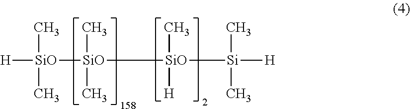
and having a viscosity of 2,000 mPa·s (H/Vi was 1.3), and 0.05 parts of a dimethylpolysiloxane solution of a vinylsiloxane chloroplatinate complex having a concentration of 1% as platinum atoms were uniformly mixed to obtain a composition. The composition was heated in an oven at 150° C. for 30 minutes to obtain a cured product with a penetration of 40.

and having a viscosity of 10,000 mPa·s, 40 parts of a both end dimethylhydrogensiloxy-blocked dimethylpolysiloxane represented by the following formula (6):

and having a viscosity of 6,000 mPa·s (H/Vi was 0.95), and 0.05 parts of a dimethylpolysiloxane solution of a vinylsiloxane chloroplatinate complex having a concentration of 1% as platinum atoms were mixed uniformly to obtain a composition. The composition was heated in an oven at 150° C. for 30 minutes to obtain a cured product with a penetration of 120.
| TABLE 1 | |||||
| Light receiving | Back | Observation | |||
| surface | surface | after | |||
| silicone | silicone | Number of | PCT severe | ||
| gel sheet | gel sheet | cracks, | deterioration test | ||
| Film | Film | detected | Number | Corrosion | Intrusion | |||||
| thickness | thickness | by EL | of | of | of | |||||
| Module | Penetration | (μm) | Penetration | (μm) | observation | cracks | tab wire | water | ||
| Example 1 | A | 75 | 200 | 75 | 200 | 0 | 1 | absent | absent |
| Example 2 | B | 75 | 500 | 75 | 500 | 0 | 0 | absent | absent |
| Example 3 | C | 75 | 800 | 75 | 800 | 0 | 0 | absent | absent |
| Example 4 | D | 40 | 200 | 40 | 200 | 1 | 2 | absent | absent |
| Example 5 | E | 40 | 500 | 40 | 500 | 0 | 0 | absent | absent |
| Example 6 | F | 40 | 800 | 40 | 800 | 0 | 0 | absent | absent |
| Example 7 | G | 120 | 200 | 120 | 200 | 1 | 2 | absent | absent |
| Example 8 | H | 120 | 500 | 120 | 500 | 1 | 1 | absent | absent |
| Example 9 | I | 120 | 800 | 120 | 800 | 0 | 0 | absent | absent |
| Example 10 | J | 75 | 500 | 40 | 500 | 0 | 0 | absent | absent |
| Comparative | K | 40 | 500 | 40 | 500 | 0 | 5 | present | present |
| Example 1 | |||||||||
| (no butyl | |||||||||
| rubber | |||||||||
| sealing) |
| Comparative | L | EVA film/ | EVA film/ | 2 | 3 | present | present |
| Example 2 | 500 μm thick | 500 μm thick | |||||
Claims (2)
RaR1 bSiO(4-a-b)/2 (1)
Applications Claiming Priority (2)
| Application Number | Priority Date | Filing Date | Title |
|---|---|---|---|
| JP2012221816A JP5867356B2 (en) | 2012-10-04 | 2012-10-04 | Manufacturing method of solar cell module |
| JP2012-221816 | 2012-10-04 |
Publications (2)
| Publication Number | Publication Date |
|---|---|
| US20140096885A1 US20140096885A1 (en) | 2014-04-10 |
| US9385253B2 true US9385253B2 (en) | 2016-07-05 |
Family
ID=50408101
Family Applications (1)
| Application Number | Title | Priority Date | Filing Date |
|---|---|---|---|
| US14/045,059 Active 2034-09-05 US9385253B2 (en) | 2012-10-04 | 2013-10-03 | Method of manufacturing solar cell module |
Country Status (5)
| Country | Link |
|---|---|
| US (1) | US9385253B2 (en) |
| JP (1) | JP5867356B2 (en) |
| KR (1) | KR102013963B1 (en) |
| CN (1) | CN103715296B (en) |
| TW (1) | TWI578559B (en) |
Families Citing this family (2)
| Publication number | Priority date | Publication date | Assignee | Title |
|---|---|---|---|---|
| DE102015103141A1 (en) * | 2015-03-04 | 2016-09-08 | Thyssenkrupp Ag | Method for producing a metal composite material with embedded functional structure and corresponding metal composite material |
| CN114899273B (en) * | 2022-04-06 | 2024-03-01 | 尚越光电科技股份有限公司 | Method for prolonging service life of flexible CIGS battery assembly and reducing cost |
Citations (35)
| Publication number | Priority date | Publication date | Assignee | Title |
|---|---|---|---|---|
| US5306797A (en) | 1990-08-01 | 1994-04-26 | Shin-Etsu Chemical Co., Ltd. | Organopolysiloxane composition and its gel cured product |
| JP2005179533A (en) | 2003-12-19 | 2005-07-07 | Ge Toshiba Silicones Co Ltd | Silicone gel composition |
| US20050250903A1 (en) | 2004-05-07 | 2005-11-10 | Shin-Etsu Chemical Co., Ltd. | Silicone gel composition |
| JP2005344106A (en) | 2004-05-07 | 2005-12-15 | Shin Etsu Chem Co Ltd | Silicone gel composition |
| US20060207646A1 (en) | 2003-07-07 | 2006-09-21 | Christine Terreau | Encapsulation of solar cells |
| US7128977B2 (en) | 2002-07-25 | 2006-10-31 | Shin-Etsu Chemical Co., Ltd. | Silicone coating composition and release sheet |
| US20060275617A1 (en) | 2005-06-07 | 2006-12-07 | Shin-Etsu Chemical Co., Ltd. | Silicone resin composition for die bonding |
| US20080276983A1 (en) | 2005-11-04 | 2008-11-13 | Robert Andrew Drake | Encapsulation of Photovoltaic Cells |
| JP2008291148A (en) | 2007-05-25 | 2008-12-04 | Shin Etsu Chem Co Ltd | Silicone gel composition excellent in heat resistance |
| JP2009515362A (en) | 2005-11-07 | 2009-04-09 | スリーエム イノベイティブ プロパティズ カンパニー | Structured heat transfer article |
| US20090159117A1 (en) | 2007-12-20 | 2009-06-25 | Truseal Technologies, Inc. | Hot melt sealant containing desiccant for use in photovoltaic modules |
| WO2009091068A1 (en) | 2008-01-15 | 2009-07-23 | Affinity Co., Ltd. | Solar cell module and method for manufacturing the same |
| US20090194156A1 (en) | 2008-02-01 | 2009-08-06 | Grommesh Robert C | Dual seal photovoltaic glazing assembly and method |
| US20090320921A1 (en) | 2008-02-01 | 2009-12-31 | Grommesh Robert C | Photovoltaic Glazing Assembly and Method |
| US20110005066A1 (en) | 2008-03-14 | 2011-01-13 | Crofoot Steven D | Method Of Forming A Photovoltaic Cell Module |
| US20110036390A1 (en) | 2009-08-11 | 2011-02-17 | Miasole | Composite encapsulants containing fillers for photovoltaic modules |
| US20110036389A1 (en) | 2009-08-11 | 2011-02-17 | Miasole | Cte modulated encapsulants for solar modules |
| US20110132437A1 (en) | 2007-12-10 | 2011-06-09 | Alan Kost | Methods to bond or seal glass pieces of photovoltaic cell modules |
| US20110139224A1 (en) | 2009-12-16 | 2011-06-16 | Miasole | Oriented reinforcement for frameless solar modules |
| US20110203665A1 (en) | 2008-11-04 | 2011-08-25 | Bridgestone Corporation | Adhesive sheet and solar cell including the same |
| US20110203642A1 (en) | 2008-12-02 | 2011-08-25 | Skc Co., Ltd. | Envelope material sheet for solar cell module and solar cell module including same |
| US20110214716A1 (en) | 2009-05-12 | 2011-09-08 | Miasole | Isolated metallic flexible back sheet for solar module encapsulation |
| US20110247674A1 (en) | 2010-04-09 | 2011-10-13 | Nitto Denko Corporation | Sealing composition, multiple glass and solar cell panel |
| US20120017980A1 (en) | 2010-07-21 | 2012-01-26 | Du Pont Apollo Limited | Photovoltaic panel and method of manufacturing the same |
| US20120129292A1 (en) | 2009-04-08 | 2012-05-24 | Saphire Solar Technologies Aps | Laminating assembly |
| WO2012112000A2 (en) | 2011-02-17 | 2012-08-23 | 주식회사 한일루브텍 | Lubricant supply device |
| US20120266943A1 (en) | 2011-04-20 | 2012-10-25 | Bo Li | Solar cell module structure and fabrication method for preventing polarization |
| US20120282727A1 (en) | 2008-08-11 | 2012-11-08 | Basol Bulent M | Method of manufacturing photovoltaic modules with improved reliability |
| US20120282725A1 (en) | 2011-05-04 | 2012-11-08 | Jongkyoung Hong | Solar cell module and method for manufacturing the same |
| US20120318354A1 (en) | 2010-12-29 | 2012-12-20 | E. I. Du Pont De Nemours And Company | Photovoltaic module with chlorosulfonated polyolefin layer |
| US20120318438A1 (en) | 2009-10-09 | 2012-12-20 | Fotoverbundglas Marl Gmbh | Device and method for producing laminated safety glass |
| US20130068279A1 (en) | 2011-09-15 | 2013-03-21 | Benyamin Buller | Photovoltaic module interlayer |
| US20130250229A1 (en) | 2010-11-19 | 2013-09-26 | Fujifilm Corporation | Birefringence pattern transfer foil |
| US20140099746A1 (en) | 2012-10-04 | 2014-04-10 | Shin-Etsu Chemical Co., Ltd. | Method of manufacturing solar cell module |
| US8999743B2 (en) | 2013-07-04 | 2015-04-07 | Shin-Etsu Chemical Co., Ltd. | Manufacture of solar cell module |
Family Cites Families (4)
| Publication number | Priority date | Publication date | Assignee | Title |
|---|---|---|---|---|
| JP3838684B2 (en) * | 1995-11-30 | 2006-10-25 | 富士電機ホールディングス株式会社 | Method for manufacturing flexible solar cell |
| US20120048348A1 (en) * | 2010-08-26 | 2012-03-01 | Fujifilm Corporation | Solar cell protective sheet and its production method, backsheet for solar cell, and solar cell module |
| WO2012113000A2 (en) * | 2011-02-21 | 2012-08-30 | Inova Lisec Technologiezentrum Gmbh | Method for producing modules |
| CN102321450A (en) * | 2011-08-23 | 2012-01-18 | 杭州之江有机硅化工有限公司 | Solar energy photovoltaic assembly organosilicon sealant material and preparation method thereof |
-
2012
- 2012-10-04 JP JP2012221816A patent/JP5867356B2/en active Active
-
2013
- 2013-09-30 KR KR1020130116025A patent/KR102013963B1/en active IP Right Grant
- 2013-09-30 CN CN201310459652.7A patent/CN103715296B/en active Active
- 2013-10-03 TW TW102135834A patent/TWI578559B/en active
- 2013-10-03 US US14/045,059 patent/US9385253B2/en active Active
Patent Citations (41)
| Publication number | Priority date | Publication date | Assignee | Title |
|---|---|---|---|---|
| US5306797A (en) | 1990-08-01 | 1994-04-26 | Shin-Etsu Chemical Co., Ltd. | Organopolysiloxane composition and its gel cured product |
| US7128977B2 (en) | 2002-07-25 | 2006-10-31 | Shin-Etsu Chemical Co., Ltd. | Silicone coating composition and release sheet |
| US20060207646A1 (en) | 2003-07-07 | 2006-09-21 | Christine Terreau | Encapsulation of solar cells |
| JP2007527109A (en) | 2003-07-07 | 2007-09-20 | ダウ・コ−ニング・コ−ポレ−ション | Solar cell encapsulation |
| JP2005179533A (en) | 2003-12-19 | 2005-07-07 | Ge Toshiba Silicones Co Ltd | Silicone gel composition |
| US20050250903A1 (en) | 2004-05-07 | 2005-11-10 | Shin-Etsu Chemical Co., Ltd. | Silicone gel composition |
| JP2005344106A (en) | 2004-05-07 | 2005-12-15 | Shin Etsu Chem Co Ltd | Silicone gel composition |
| US20060275617A1 (en) | 2005-06-07 | 2006-12-07 | Shin-Etsu Chemical Co., Ltd. | Silicone resin composition for die bonding |
| US20080276983A1 (en) | 2005-11-04 | 2008-11-13 | Robert Andrew Drake | Encapsulation of Photovoltaic Cells |
| JP2009515365A (en) | 2005-11-04 | 2009-04-09 | ダウ・コーニング・コーポレイション | Photovoltaic encapsulation |
| JP2009515362A (en) | 2005-11-07 | 2009-04-09 | スリーエム イノベイティブ プロパティズ カンパニー | Structured heat transfer article |
| JP2008291148A (en) | 2007-05-25 | 2008-12-04 | Shin Etsu Chem Co Ltd | Silicone gel composition excellent in heat resistance |
| US20110132437A1 (en) | 2007-12-10 | 2011-06-09 | Alan Kost | Methods to bond or seal glass pieces of photovoltaic cell modules |
| US20090159117A1 (en) | 2007-12-20 | 2009-06-25 | Truseal Technologies, Inc. | Hot melt sealant containing desiccant for use in photovoltaic modules |
| WO2009091068A1 (en) | 2008-01-15 | 2009-07-23 | Affinity Co., Ltd. | Solar cell module and method for manufacturing the same |
| US20100275992A1 (en) | 2008-01-15 | 2010-11-04 | Affinity Co., Ltd. | Solar Cell Module and Process for its Production |
| US20090194156A1 (en) | 2008-02-01 | 2009-08-06 | Grommesh Robert C | Dual seal photovoltaic glazing assembly and method |
| US20090320921A1 (en) | 2008-02-01 | 2009-12-31 | Grommesh Robert C | Photovoltaic Glazing Assembly and Method |
| US20110061724A1 (en) | 2008-03-14 | 2011-03-17 | Kevin Houle | Photovoltaic Cell Module And Method Of Forming Same |
| JP2011514680A (en) | 2008-03-14 | 2011-05-06 | ダウ・コーニング・コーポレイション | Method for forming photovoltaic cell module |
| US20110005066A1 (en) | 2008-03-14 | 2011-01-13 | Crofoot Steven D | Method Of Forming A Photovoltaic Cell Module |
| US20120282727A1 (en) | 2008-08-11 | 2012-11-08 | Basol Bulent M | Method of manufacturing photovoltaic modules with improved reliability |
| US20110203665A1 (en) | 2008-11-04 | 2011-08-25 | Bridgestone Corporation | Adhesive sheet and solar cell including the same |
| US20110203642A1 (en) | 2008-12-02 | 2011-08-25 | Skc Co., Ltd. | Envelope material sheet for solar cell module and solar cell module including same |
| US20120129292A1 (en) | 2009-04-08 | 2012-05-24 | Saphire Solar Technologies Aps | Laminating assembly |
| US20110214716A1 (en) | 2009-05-12 | 2011-09-08 | Miasole | Isolated metallic flexible back sheet for solar module encapsulation |
| US20110036390A1 (en) | 2009-08-11 | 2011-02-17 | Miasole | Composite encapsulants containing fillers for photovoltaic modules |
| US20110036389A1 (en) | 2009-08-11 | 2011-02-17 | Miasole | Cte modulated encapsulants for solar modules |
| US20120318438A1 (en) | 2009-10-09 | 2012-12-20 | Fotoverbundglas Marl Gmbh | Device and method for producing laminated safety glass |
| US20110139224A1 (en) | 2009-12-16 | 2011-06-16 | Miasole | Oriented reinforcement for frameless solar modules |
| US20110247674A1 (en) | 2010-04-09 | 2011-10-13 | Nitto Denko Corporation | Sealing composition, multiple glass and solar cell panel |
| JP2011231309A (en) | 2010-04-09 | 2011-11-17 | Nitto Denko Corp | Sealing composition, double glazing and solar cell panel |
| US20120017980A1 (en) | 2010-07-21 | 2012-01-26 | Du Pont Apollo Limited | Photovoltaic panel and method of manufacturing the same |
| US20130250229A1 (en) | 2010-11-19 | 2013-09-26 | Fujifilm Corporation | Birefringence pattern transfer foil |
| US20120318354A1 (en) | 2010-12-29 | 2012-12-20 | E. I. Du Pont De Nemours And Company | Photovoltaic module with chlorosulfonated polyolefin layer |
| WO2012112000A2 (en) | 2011-02-17 | 2012-08-23 | 주식회사 한일루브텍 | Lubricant supply device |
| US20120266943A1 (en) | 2011-04-20 | 2012-10-25 | Bo Li | Solar cell module structure and fabrication method for preventing polarization |
| US20120282725A1 (en) | 2011-05-04 | 2012-11-08 | Jongkyoung Hong | Solar cell module and method for manufacturing the same |
| US20130068279A1 (en) | 2011-09-15 | 2013-03-21 | Benyamin Buller | Photovoltaic module interlayer |
| US20140099746A1 (en) | 2012-10-04 | 2014-04-10 | Shin-Etsu Chemical Co., Ltd. | Method of manufacturing solar cell module |
| US8999743B2 (en) | 2013-07-04 | 2015-04-07 | Shin-Etsu Chemical Co., Ltd. | Manufacture of solar cell module |
Non-Patent Citations (8)
| Title |
|---|
| Ketola, B., et al., "Demonstration of the Benefits of Silicone Encapsulation of PV Modules in a Large Scale Outdoor Array", Dow Corning Corporation. |
| Notification of Reasons for Rejection dated Aug. 18, 2015, issued in counterpart Japanese Patent Application No. 2012-221816 (2 pages). |
| Office Action dated Apr. 20, 2015, issued in U.S. Appl. No. 13/904,569 (26 pages). |
| Office Action dated Feb. 28, 2014 issued in U.S. Appl. No. 13/904,569 (23 pages). |
| Office Action dated May 19, 2015, issued in Japanese Patent Application No. 2012-121475 (2 pages) (counterpart to U.S. Appl. No. 13/904,569). |
| Office Action dated Nov. 4, 2015, issued in U.S. Appl. No. 14/045,352 (10 pages). |
| Ohl, S., et al., "Increased Internal Quantum Efficiency of Encapsulated Solar Cell by Using Two-Component Silicone as Encapsulant Material", Proc. 23rd, EU PVSEC, Valencia (2008), pp. 2693-2697. |
| U.S. Office Action dated Nov. 24, 2014, issued in U.S. Appl. No. 13/904,569 (23 pages). |
Also Published As
| Publication number | Publication date |
|---|---|
| JP5867356B2 (en) | 2016-02-24 |
| US20140096885A1 (en) | 2014-04-10 |
| CN103715296A (en) | 2014-04-09 |
| TW201428990A (en) | 2014-07-16 |
| TWI578559B (en) | 2017-04-11 |
| JP2014075464A (en) | 2014-04-24 |
| KR20140044740A (en) | 2014-04-15 |
| CN103715296B (en) | 2017-07-04 |
| KR102013963B1 (en) | 2019-08-23 |
Similar Documents
| Publication | Publication Date | Title |
|---|---|---|
| KR101952970B1 (en) | Method for producing a solar cell module | |
| US9520522B2 (en) | Method of manufacturing solar cell module | |
| EP3070748B1 (en) | Silicone adhesive sheet having ultraviolet ray shielding properties for sealing solar cell and solar cell module using same | |
| US9299875B2 (en) | Manufacture of solar cell module | |
| US8999743B2 (en) | Manufacture of solar cell module | |
| EP2930214A1 (en) | Solar cell encapsulant silicone composition and solar cell module | |
| US20150000738A1 (en) | Solar cell module and making method | |
| US9385253B2 (en) | Method of manufacturing solar cell module | |
| KR102165215B1 (en) | Silicone adhesive sheet for sealing a solar cell and method for producing a solar cell module using the same | |
| JP6269527B2 (en) | Manufacturing method of solar cell module | |
| JP2015018892A (en) | Method for manufacturing solar cell module | |
| JP6070527B2 (en) | Manufacturing method of solar cell module | |
| JP2017191813A (en) | Solar battery module and manufacturing method for the same |
Legal Events
| Date | Code | Title | Description |
|---|---|---|---|
| AS | Assignment |
Owner name: SHIN-ETSU CHEMICAL CO., LTD., JAPAN Free format text: ASSIGNMENT OF ASSIGNORS INTEREST;ASSIGNORS:FURIHATA, TOMOYOSHI;ITO, ATSUO;OHWADA, HIROTO;AND OTHERS;REEL/FRAME:031341/0380 Effective date: 20130920 |
|
| STCF | Information on status: patent grant |
Free format text: PATENTED CASE |
|
| MAFP | Maintenance fee payment |
Free format text: PAYMENT OF MAINTENANCE FEE, 4TH YEAR, LARGE ENTITY (ORIGINAL EVENT CODE: M1551); ENTITY STATUS OF PATENT OWNER: LARGE ENTITY Year of fee payment: 4 |
|
| FEPP | Fee payment procedure |
Free format text: MAINTENANCE FEE REMINDER MAILED (ORIGINAL EVENT CODE: REM.); ENTITY STATUS OF PATENT OWNER: LARGE ENTITY |