US9373636B2 - Methods of forming semiconductor constructions - Google Patents
Methods of forming semiconductor constructions Download PDFInfo
- Publication number
- US9373636B2 US9373636B2 US14/930,504 US201514930504A US9373636B2 US 9373636 B2 US9373636 B2 US 9373636B2 US 201514930504 A US201514930504 A US 201514930504A US 9373636 B2 US9373636 B2 US 9373636B2
- Authority
- US
- United States
- Prior art keywords
- dielectric material
- trenches
- panels
- forming
- stack
- Prior art date
- Legal status (The legal status is an assumption and is not a legal conclusion. Google has not performed a legal analysis and makes no representation as to the accuracy of the status listed.)
- Active
Links
- 238000000034 method Methods 0.000 title claims abstract description 30
- 238000010276 construction Methods 0.000 title claims abstract description 19
- 239000004065 semiconductor Substances 0.000 title claims abstract description 19
- 239000000463 material Substances 0.000 claims abstract description 137
- 239000003989 dielectric material Substances 0.000 claims abstract description 112
- 239000011232 storage material Substances 0.000 claims abstract description 29
- 230000008878 coupling Effects 0.000 claims 2
- 238000010168 coupling process Methods 0.000 claims 2
- 238000005859 coupling reaction Methods 0.000 claims 2
- VYPSYNLAJGMNEJ-UHFFFAOYSA-N Silicium dioxide Chemical compound O=[Si]=O VYPSYNLAJGMNEJ-UHFFFAOYSA-N 0.000 description 22
- 239000000203 mixture Substances 0.000 description 18
- 235000012239 silicon dioxide Nutrition 0.000 description 11
- 239000000377 silicon dioxide Substances 0.000 description 11
- XUIMIQQOPSSXEZ-UHFFFAOYSA-N Silicon Chemical compound [Si] XUIMIQQOPSSXEZ-UHFFFAOYSA-N 0.000 description 8
- 229910052710 silicon Inorganic materials 0.000 description 8
- 239000010703 silicon Substances 0.000 description 8
- 238000004519 manufacturing process Methods 0.000 description 7
- 229910052581 Si3N4 Inorganic materials 0.000 description 5
- 238000000231 atomic layer deposition Methods 0.000 description 5
- 229910052751 metal Inorganic materials 0.000 description 5
- 239000002184 metal Substances 0.000 description 5
- HQVNEWCFYHHQES-UHFFFAOYSA-N silicon nitride Chemical compound N12[Si]34N5[Si]62N3[Si]51N64 HQVNEWCFYHHQES-UHFFFAOYSA-N 0.000 description 5
- 239000000758 substrate Substances 0.000 description 5
- 238000005229 chemical vapour deposition Methods 0.000 description 4
- 238000005240 physical vapour deposition Methods 0.000 description 4
- 229910021420 polycrystalline silicon Inorganic materials 0.000 description 3
- 238000000429 assembly Methods 0.000 description 2
- 230000000712 assembly Effects 0.000 description 2
- 230000015572 biosynthetic process Effects 0.000 description 2
- 238000004891 communication Methods 0.000 description 2
- -1 etc.) Substances 0.000 description 2
- 229910015844 BCl3 Inorganic materials 0.000 description 1
- CPELXLSAUQHCOX-UHFFFAOYSA-N Hydrogen bromide Chemical compound Br CPELXLSAUQHCOX-UHFFFAOYSA-N 0.000 description 1
- RTAQQCXQSZGOHL-UHFFFAOYSA-N Titanium Chemical compound [Ti] RTAQQCXQSZGOHL-UHFFFAOYSA-N 0.000 description 1
- VQLOCUKZAJRPAO-UHFFFAOYSA-N aluminum oxygen(2-) tantalum(5+) Chemical compound [O--].[O--].[O--].[O--].[Al+3].[Ta+5] VQLOCUKZAJRPAO-UHFFFAOYSA-N 0.000 description 1
- 230000004888 barrier function Effects 0.000 description 1
- 238000013500 data storage Methods 0.000 description 1
- 238000009792 diffusion process Methods 0.000 description 1
- RWRIWBAIICGTTQ-UHFFFAOYSA-N difluoromethane Chemical compound FCF RWRIWBAIICGTTQ-UHFFFAOYSA-N 0.000 description 1
- 238000005530 etching Methods 0.000 description 1
- 229910052732 germanium Inorganic materials 0.000 description 1
- GNPVGFCGXDBREM-UHFFFAOYSA-N germanium atom Chemical compound [Ge] GNPVGFCGXDBREM-UHFFFAOYSA-N 0.000 description 1
- 229910000449 hafnium oxide Inorganic materials 0.000 description 1
- WIHZLLGSGQNAGK-UHFFFAOYSA-N hafnium(4+);oxygen(2-) Chemical compound [O-2].[O-2].[Hf+4] WIHZLLGSGQNAGK-UHFFFAOYSA-N 0.000 description 1
- 239000012212 insulator Substances 0.000 description 1
- 238000002955 isolation Methods 0.000 description 1
- 238000005259 measurement Methods 0.000 description 1
- 150000002739 metals Chemical class 0.000 description 1
- 229910021421 monocrystalline silicon Inorganic materials 0.000 description 1
- 150000004767 nitrides Chemical class 0.000 description 1
- GVGCUCJTUSOZKP-UHFFFAOYSA-N nitrogen trifluoride Chemical compound FN(F)F GVGCUCJTUSOZKP-UHFFFAOYSA-N 0.000 description 1
- 230000003647 oxidation Effects 0.000 description 1
- 238000007254 oxidation reaction Methods 0.000 description 1
- RVTZCBVAJQQJTK-UHFFFAOYSA-N oxygen(2-);zirconium(4+) Chemical compound [O-2].[O-2].[Zr+4] RVTZCBVAJQQJTK-UHFFFAOYSA-N 0.000 description 1
- 229920002120 photoresistant polymer Polymers 0.000 description 1
- 229920005591 polysilicon Polymers 0.000 description 1
- 239000003870 refractory metal Substances 0.000 description 1
- 229910021332 silicide Inorganic materials 0.000 description 1
- FVBUAEGBCNSCDD-UHFFFAOYSA-N silicide(4-) Chemical compound [Si-4] FVBUAEGBCNSCDD-UHFFFAOYSA-N 0.000 description 1
- 239000007787 solid Substances 0.000 description 1
- 229910052719 titanium Inorganic materials 0.000 description 1
- 239000010936 titanium Substances 0.000 description 1
- FAQYAMRNWDIXMY-UHFFFAOYSA-N trichloroborane Chemical compound ClB(Cl)Cl FAQYAMRNWDIXMY-UHFFFAOYSA-N 0.000 description 1
- WFKWXMTUELFFGS-UHFFFAOYSA-N tungsten Chemical compound [W] WFKWXMTUELFFGS-UHFFFAOYSA-N 0.000 description 1
- 229910052721 tungsten Inorganic materials 0.000 description 1
- 239000010937 tungsten Substances 0.000 description 1
- 229910001928 zirconium oxide Inorganic materials 0.000 description 1
Images


Classifications
-
- H01L27/11582—
-
- H01L27/11524—
-
- H01L27/11556—
-
- H01L27/1157—
-
- H—ELECTRICITY
- H01—ELECTRIC ELEMENTS
- H01L—SEMICONDUCTOR DEVICES NOT COVERED BY CLASS H10
- H01L29/00—Semiconductor devices adapted for rectifying, amplifying, oscillating or switching, or capacitors or resistors with at least one potential-jump barrier or surface barrier, e.g. PN junction depletion layer or carrier concentration layer; Details of semiconductor bodies or of electrodes thereof ; Multistep manufacturing processes therefor
- H01L29/66—Types of semiconductor device ; Multistep manufacturing processes therefor
- H01L29/66007—Multistep manufacturing processes
- H01L29/66075—Multistep manufacturing processes of devices having semiconductor bodies comprising group 14 or group 13/15 materials
- H01L29/66227—Multistep manufacturing processes of devices having semiconductor bodies comprising group 14 or group 13/15 materials the devices being controllable only by the electric current supplied or the electric potential applied, to an electrode which does not carry the current to be rectified, amplified or switched, e.g. three-terminal devices
- H01L29/66409—Unipolar field-effect transistors
- H01L29/66477—Unipolar field-effect transistors with an insulated gate, i.e. MISFET
- H01L29/66825—Unipolar field-effect transistors with an insulated gate, i.e. MISFET with a floating gate
-
- H—ELECTRICITY
- H01—ELECTRIC ELEMENTS
- H01L—SEMICONDUCTOR DEVICES NOT COVERED BY CLASS H10
- H01L29/00—Semiconductor devices adapted for rectifying, amplifying, oscillating or switching, or capacitors or resistors with at least one potential-jump barrier or surface barrier, e.g. PN junction depletion layer or carrier concentration layer; Details of semiconductor bodies or of electrodes thereof ; Multistep manufacturing processes therefor
- H01L29/66—Types of semiconductor device ; Multistep manufacturing processes therefor
- H01L29/66007—Multistep manufacturing processes
- H01L29/66075—Multistep manufacturing processes of devices having semiconductor bodies comprising group 14 or group 13/15 materials
- H01L29/66227—Multistep manufacturing processes of devices having semiconductor bodies comprising group 14 or group 13/15 materials the devices being controllable only by the electric current supplied or the electric potential applied, to an electrode which does not carry the current to be rectified, amplified or switched, e.g. three-terminal devices
- H01L29/66409—Unipolar field-effect transistors
- H01L29/66477—Unipolar field-effect transistors with an insulated gate, i.e. MISFET
- H01L29/66833—Unipolar field-effect transistors with an insulated gate, i.e. MISFET with a charge trapping gate insulator, e.g. MNOS transistors
-
- H—ELECTRICITY
- H01—ELECTRIC ELEMENTS
- H01L—SEMICONDUCTOR DEVICES NOT COVERED BY CLASS H10
- H01L29/00—Semiconductor devices adapted for rectifying, amplifying, oscillating or switching, or capacitors or resistors with at least one potential-jump barrier or surface barrier, e.g. PN junction depletion layer or carrier concentration layer; Details of semiconductor bodies or of electrodes thereof ; Multistep manufacturing processes therefor
- H01L29/66—Types of semiconductor device ; Multistep manufacturing processes therefor
- H01L29/68—Types of semiconductor device ; Multistep manufacturing processes therefor controllable by only the electric current supplied, or only the electric potential applied, to an electrode which does not carry the current to be rectified, amplified or switched
- H01L29/76—Unipolar devices, e.g. field effect transistors
- H01L29/772—Field effect transistors
- H01L29/78—Field effect transistors with field effect produced by an insulated gate
- H01L29/788—Field effect transistors with field effect produced by an insulated gate with floating gate
- H01L29/7889—Vertical transistors, i.e. transistors having source and drain not in the same horizontal plane
-
- H—ELECTRICITY
- H01—ELECTRIC ELEMENTS
- H01L—SEMICONDUCTOR DEVICES NOT COVERED BY CLASS H10
- H01L29/00—Semiconductor devices adapted for rectifying, amplifying, oscillating or switching, or capacitors or resistors with at least one potential-jump barrier or surface barrier, e.g. PN junction depletion layer or carrier concentration layer; Details of semiconductor bodies or of electrodes thereof ; Multistep manufacturing processes therefor
- H01L29/66—Types of semiconductor device ; Multistep manufacturing processes therefor
- H01L29/68—Types of semiconductor device ; Multistep manufacturing processes therefor controllable by only the electric current supplied, or only the electric potential applied, to an electrode which does not carry the current to be rectified, amplified or switched
- H01L29/76—Unipolar devices, e.g. field effect transistors
- H01L29/772—Field effect transistors
- H01L29/78—Field effect transistors with field effect produced by an insulated gate
- H01L29/792—Field effect transistors with field effect produced by an insulated gate with charge trapping gate insulator, e.g. MNOS-memory transistors
- H01L29/7926—Vertical transistors, i.e. transistors having source and drain not in the same horizontal plane
-
- H—ELECTRICITY
- H10—SEMICONDUCTOR DEVICES; ELECTRIC SOLID-STATE DEVICES NOT OTHERWISE PROVIDED FOR
- H10B—ELECTRONIC MEMORY DEVICES
- H10B41/00—Electrically erasable-and-programmable ROM [EEPROM] devices comprising floating gates
- H10B41/20—Electrically erasable-and-programmable ROM [EEPROM] devices comprising floating gates characterised by three-dimensional arrangements, e.g. with cells on different height levels
- H10B41/23—Electrically erasable-and-programmable ROM [EEPROM] devices comprising floating gates characterised by three-dimensional arrangements, e.g. with cells on different height levels with source and drain on different levels, e.g. with sloping channels
- H10B41/27—Electrically erasable-and-programmable ROM [EEPROM] devices comprising floating gates characterised by three-dimensional arrangements, e.g. with cells on different height levels with source and drain on different levels, e.g. with sloping channels the channels comprising vertical portions, e.g. U-shaped channels
-
- H—ELECTRICITY
- H10—SEMICONDUCTOR DEVICES; ELECTRIC SOLID-STATE DEVICES NOT OTHERWISE PROVIDED FOR
- H10B—ELECTRONIC MEMORY DEVICES
- H10B41/00—Electrically erasable-and-programmable ROM [EEPROM] devices comprising floating gates
- H10B41/30—Electrically erasable-and-programmable ROM [EEPROM] devices comprising floating gates characterised by the memory core region
- H10B41/35—Electrically erasable-and-programmable ROM [EEPROM] devices comprising floating gates characterised by the memory core region with a cell select transistor, e.g. NAND
-
- H—ELECTRICITY
- H10—SEMICONDUCTOR DEVICES; ELECTRIC SOLID-STATE DEVICES NOT OTHERWISE PROVIDED FOR
- H10B—ELECTRONIC MEMORY DEVICES
- H10B43/00—EEPROM devices comprising charge-trapping gate insulators
- H10B43/20—EEPROM devices comprising charge-trapping gate insulators characterised by three-dimensional arrangements, e.g. with cells on different height levels
- H10B43/23—EEPROM devices comprising charge-trapping gate insulators characterised by three-dimensional arrangements, e.g. with cells on different height levels with source and drain on different levels, e.g. with sloping channels
- H10B43/27—EEPROM devices comprising charge-trapping gate insulators characterised by three-dimensional arrangements, e.g. with cells on different height levels with source and drain on different levels, e.g. with sloping channels the channels comprising vertical portions, e.g. U-shaped channels
-
- H—ELECTRICITY
- H10—SEMICONDUCTOR DEVICES; ELECTRIC SOLID-STATE DEVICES NOT OTHERWISE PROVIDED FOR
- H10B—ELECTRONIC MEMORY DEVICES
- H10B43/00—EEPROM devices comprising charge-trapping gate insulators
- H10B43/30—EEPROM devices comprising charge-trapping gate insulators characterised by the memory core region
- H10B43/35—EEPROM devices comprising charge-trapping gate insulators characterised by the memory core region with cell select transistors, e.g. NAND
Definitions
- Flash memory provides data storage for electronic systems. Flash memory is one type of memory, and has numerous uses in modern computers and devices. For instance, modern personal computers may have BIOS stored on a flash memory chip. As another example, it is becoming increasingly common for computers and other devices to utilize flash memory in solid state drives to replace conventional hard drives. As yet another example, flash memory is popular in wireless electronic devices because it enables the manufacturer to support new communication protocols as they become standardized, and to provide the ability to remotely upgrade the devices for enhanced features.
- a typical flash memory comprises a memory array that includes a large number of memory cells arranged in row and column fashion.
- the flash memory may be erased and reprogrammed in blocks.
- NAND may be a basic architecture of flash memory.
- a NAND comprises at least one selecting device coupled in series to a serial combination of memory cells.
- Example NAND architecture is described in U.S. Pat. No. 7,898,850.
- FIGS. 1-19 are diagrammatic cross-sectional views of a semiconductor construction at various process stages of an example embodiment.
- FIGS. 1, 3, 5, 7, 9, 11, 13, 15 and 17 are top views;
- FIGS. 2, 4, 6, 8, 10, 12, 14, 16 and 18 are cross-sectional side views along the line X-X of FIGS. 1, 3, 5, 7, 9, 11, 13, 15 and 17 , respectively;
- FIG. 19 is a diagrammatic cross-sectional view of the construction of FIG. 18 shown at a process stage subsequent to that of FIG. 18 .
- NAND architecture may be fabricated to comprise substantially vertical NAND strings.
- the fabrication may utilize line and space patterns for formation of channel regions and isolation regions, which can advantageously avoid difficulties encountered in conventional NAND fabrication processes utilizing pillars (or other high aspect ratio contacts) to support channel regions.
- new NAND architectures may result from processes described herein. Although NAND architectures are described in some example embodiments presented herein, in other embodiments processing described herein may be utilized for fabrication of other memory, such as, for example, NOR, etc. Some example embodiments are described with reference to FIGS. 1-19 .
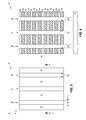
- FIGS. 1 and 2 a semiconductor construction 10 is shown in top view ( FIG. 1 ) and cross-sectional side view ( FIG. 2 ).
- the construction 10 includes a stack 14 supported by a base 12 .
- Stack 14 comprises alternating levels (e.g., sheets, layers, etc.) of control gate material 16 and intervening dielectric material 18 . Dashed lines are provided between the stack 14 and the base 12 to indicate that there may be additional materials and/or integrated circuit structures between the base and the stack in some embodiments.
- the base 12 may comprise semiconductor material, and in some embodiments may comprise, consist essentially of, or consist of monocrystalline silicon. In some embodiments, base 12 may be considered to comprise a semiconductor substrate.
- semiconductor substrate means any construction comprising semiconductive material, including, but not limited to, bulk semiconductive materials such as a semiconductive wafer (either alone or in assemblies comprising other materials), and semiconductive material layers (either alone or in assemblies comprising other materials).
- substrate refers to any supporting structure, including, but not limited to, the semiconductor substrates described above.
- base 12 may correspond to a semiconductor substrate containing one or more materials associated with integrated circuit fabrication. Such materials may include, for example, one or more of refractory metal materials, barrier materials, diffusion materials, insulator materials, etc.
- Control gate material 16 may comprise any suitable composition or combination of compositions; and in some embodiments may comprise, consist essentially of, or consist of one or more of various metals (for example, tungsten, titanium, etc.), metal-containing compositions (for instance, metal nitride, metal carbide, metal silicide, etc.), and conductively-doped semiconductor materials (for instance, conductively-doped silicon, conductively-doped germanium, etc.).
- the control gate material 16 may comprise, consist essentially of, or consist of conductively-doped silicon; such as, for example, n-type doped polycrystalline silicon.
- the intervening dielectric material 18 may comprise any suitable composition; and in some embodiments may comprise, consist essentially of, or consist of silicon dioxide.
- the levels of control gate material 16 may be of any suitable thickness (T 1 ), and in some embodiments may have a thickness within a range of from about 5 nm to about 300 nm.
- the levels of intervening dielectric material 18 may be of any suitable thickness (T 2 ), and in some embodiments may have a thickness within a range of from about 5 nm to about 200 nm.
- the example processing described herein forms vertical NAND strings, with the number of memory cells in each string been determined by the number of control gate levels.
- the shown example embodiment has eight levels of control gate material 16 .
- Other embodiments may have more or less than the shown eight levels. Accordingly, other example embodiments may have a stack with a total of 16 control gate levels, 32 control gate levels, 64 control gate levels, etc.
- the stack 14 is etched to form a plurality of first trenches 20 - 22 within the stack.
- the first trenches extend along a first direction of an axis 5 , as shown in the top view of FIG. 3 .
- the first trenches are configured as lines extending along the axis 5 .
- the first trenches may form structures which are curved or wavy along axis 5 , rather than being straight lines, but may still extend primarily along the direction of axis 5 .
- the first trenches 20 - 22 may have any suitable widths (W), and in some embodiments may have widths within a range of from about 5 nm to about 100 nm.
- the trenches 20 - 22 may be formed with any suitable processing.
- a mask (not shown) may be formed across a top of construction 10 to define locations of the trenches, and then one or more suitable etches may be utilized to pattern the trenches through stack 14 (in some example embodiments, the etching used to form trenches 20 - 22 may utilize one or more of NF 3 , CH 2 F 2 , HBr and BCl 3 ). Subsequently, the patterned mask may be removed to leave the illustrated construction of FIGS. 3 and 4 .
- the patterned mask may comprise any suitable material and may be formed utilizing any suitable processing.
- the patterned mask may comprise photolithographically-patterned photoresist and/or the patterned mask may comprise material patterned through a pitch-multiplication process.
- the trenches 20 - 22 may be considered to comprise interior walls 23 (only some of which are labeled) which extend along the materials 16 and 18 of stack 14 .
- the control gate material 16 is recessed along the interior walls of trenches 20 - 22 to form a plurality of cavities 24 (only some of which are labeled).
- the individual cavities are bounded on top and bottom by intervening dielectric material 18 , and are bounded along one side by control gate material 16 .
- some of the cavities have the tops and bottoms labeled as 25 and 27 , respectively; and some of the cavities have the side bounded by the control gate material labeled as 29 .
- the cavities may be recessed to any suitable distance (D) into the control gate material 16 , and in some embodiments may be recessed to a distance within a range of from about 5 nm to about 100 nm.
- cell dielectric material 26 (only some of which is labeled) is formed within cavities 24 along exposed edges of control gate material 16 .
- the cell dielectric material 26 may be referred to as a first cell dielectric material to distinguish it from other cell dielectric materials that are subsequently formed (discussed below).
- the cell dielectric material 26 may comprise any suitable composition or combination of compositions; and in some embodiments may comprise, consist essentially of, or consist of silicon dioxide. Such silicon dioxide may be thermally grown from silicon of control gate material 16 in embodiments in which the control gate material comprises, consists essentially of, or consists of silicon. Alternatively, or additionally, at least some of the cell dielectric material may be deposited.
- the cell dielectric 26 may be formed to any suitable thickness, and in some example embodiments may be formed to a thickness within a range of from about 10 ⁇ to about 200 ⁇ .
- second cell dielectric material 28 (only some of which is labeled) is formed directly adjacent the first cell dielectric material 26 .
- the second cell dielectric material within cavities 24 may be considered to be shaped as containers having open ends pointing away from the adjacent first cell dielectric material 26 .
- the second cell dielectric material 28 may comprise any suitable composition or combination of compositions; and in some embodiments may comprise, consist essentially of, or consist of silicon nitride.
- the second cell dielectric material may be formed utilizing any suitable processing, such as, for example, one or more of atomic layer deposition (ALD), chemical vapor deposition (CVD) and physical vapor deposition (PVD). It may be advantageous that the second cell dielectric material be formed conformally, as shown, and thus it may be advantageous to utilize ALD for forming such material in some embodiments.
- ALD atomic layer deposition
- CVD chemical vapor deposition
- PVD physical vapor deposition
- the intervening dielectric material 18 has surfaces 31 (only some of which are labeled) along trenches 20 - 22 .
- the second cell dielectric 28 extends within cavities 24 , and along surfaces 31 of dielectric material 18 .
- material 28 be removed from surfaces 31 with an appropriate etch following formation of material 28 within cavities 24 .
- Material 28 may be formed to any suitable thickness, and in some example embodiments may be formed to a thickness within a range of from about 50 ⁇ to about 200 ⁇ .
- a third cell dielectric 30 (only some of which is labeled) is formed within the containers defined by the second cell dielectric 28 .
- the second cell dielectric material 28 may comprise, consist essentially of, or consist of silicon nitride; and the third cell dielectric 30 may comprise, consist essentially of, or consist of silicon dioxide.
- the first and third cell dielectrics 26 and 30 may comprise the same composition as one another; and may, for example, both comprise, consist essentially of, or consist of silicon dioxide.
- the third cell dielectric may be thermally grown from the silicon nitride, and/or may be deposited over the silicon nitride.
- the third cell dielectric 30 may comprise any suitable thickness, and in some example embodiments may be formed to a thickness within a range of from about 10 ⁇ to about 100 ⁇ .
- charge-storage material 32 (only some of which is labeled) is formed within the containers defined by material 28 , and directly against material 30 in the shown embodiment.
- the third cell dielectric 30 may be considered to partially fill the containers defined by the second cell dielectric 28
- the charge-storage material 32 may be considered to be formed within such partially-filled containers.
- the charge-storage material may comprise any material suitable for retaining charge in memory cells.
- the charge-storage material may comprise, consist essentially of, or consist of appropriately-doped polycrystalline silicon, and may thus be utilized to form floating gates of memory cells.
- the charge-storage material may comprise charge-trapping material, such as, for example, silicon nitride, silicon oxynitride, conductive nanodots, etc.
- the cell dielectrics 26 , 28 and 30 together with the charge-storage material 32 , form memory cell stacks 36 (only some of which are labeled) within the cavities 24 (the cavities are labeled in previous figures, such as, for example, FIG. 6 ). Although the shown embodiment utilizes three cell dielectrics within the memory cell stacks, in other embodiments other numbers of cell dielectrics may be used. Generally, there will be at least one cell dielectric.
- gate dielectric material 38 is formed along interior sidewalls of the trenches 20 - 22 , and then channel material 40 is formed within such trenches.
- the gate dielectric material 38 may comprise any suitable composition or combination of compositions; and in some embodiments may comprise, consist essentially of, or consist of one or more of silicon dioxide, tantalum aluminum oxide, hafnium oxide, zirconium oxide, etc. In some embodiments, the gate dielectric material may comprise a same composition as cell dielectric 26 . For example, in some embodiments the gate dielectric 38 and the cell dielectric 26 may each comprise, consist essentially of, or consist of silicon dioxide.
- the gate dielectric material 38 may be formed with any suitable processing including, for example, one or more of ALD, CVD and PVD.
- the gate dielectric material may be formed to any suitable thickness, including, for example, a thickness within a range of from about 10 ⁇ to about 50 ⁇ . In the shown embodiment, the gate dielectric material extends across the open ends of the containers defined by material 28 , and extends across the charge-storage material 32 .
- the charge-storage material 32 comprises silicon
- the gate dielectric material 38 comprises silicon dioxide formed by thermal oxidation of such silicon.
- the gate dielectric material may be only along surfaces of material 32 , rather than entirely along the sidewalls of the trenches.
- the channel material 40 may comprise any suitable composition or combination of compositions; and in some embodiments may comprise, consist essentially of, or consist of appropriately-doped silicon (e.g., conductively-doped polysilicon).
- the channel material may be formed with any suitable processing, including, for example, one or more of ALD, CVD and PVD.
- the channel material 40 may be considered to form panels 50 - 52 within the trenches 20 - 22 , respectively. Such channel material panels extend along the direction of axis 5 . In some embodiments, the channel material panels may be considered to divide stack 14 into sections. Each channel panel may form a first section on a first side of the channel panel, and a second section on a second side of the channel panel, with the second side being in opposing relation to the first side.
- a plurality of second trenches 54 - 57 are formed within the stack 14 , and extend along the direction of axis 5 as shown in the top view of FIG. 17 .
- the trenches 54 - 57 may be formed with any suitable processing, including, for example, processing analogous to that described above with reference to FIGS. 3 and for fabrication of the first trenches 20 - 22 . Accordingly, in some embodiments a patterned mask (not shown) may be formed over stack 14 , a pattern transferred from the patterned mask into the stack 14 to form the trenches 54 - 57 , and then the mask may be removed.
- the second trenches are filled with dielectric material 60 .
- dielectric material may comprise any suitable composition or combination of compositions; and in some embodiments may comprise, consist essentially of, or consist of silicon dioxide.
- the dielectric material 60 may be considered to form dielectric material panels 104 - 107 within the trenches 54 - 57 .
- FIGS. 17 and 18 also show a plurality of third trenches 61 - 78 formed within stack 14 and channel material 40 .
- the third trenches extend along an axis 7 which is substantially orthogonal to the axis 5 in the shown embodiment; with the term “substantially orthogonal” meaning that the axes 5 and 7 are orthogonal to within reasonable tolerances of fabrication and measurement.
- the trenches 61 - 78 may be formed with any suitable processing, including, for example, processing analogous to that described above with reference to FIGS. 3 and 4 for fabrication of the first trenches 20 - 22 . Accordingly, in some embodiments a patterned mask (not shown) may be formed over stack 14 , a pattern transferred from the patterned mask into the stack 14 and channel material 40 to form the trenches 61 - 78 , and then the mask may be removed.
- the third trenches are filled with dielectric material 80 .
- dielectric material may comprise a suitable composition or combination of compositions; and in some embodiments may comprise, consist essentially of, or consist of silicon dioxide.
- the dielectric material 80 may be considered to form dielectric material panels 108 - 125 within the trenches 61 - 78 .
- the dielectric material panels 104 - 107 may be referred to as first dielectric material panels, and the dielectric material panels 108 - 125 may be referred to as second dielectric material panels.
- the second dielectric material panels are thicker than the first dielectric material panels.
- the first and second dielectric material panels may be the same thicknesses as one another, or the first dielectric material panels may be thicker than the second dielectric material panels.
- the trenches 54 - 57 may be formed prior to the trenches 61 - 78 ; in other embodiments the trenches 61 - 78 may be formed prior to the trenches 54 - 57 ; and in yet other embodiments the trenches 61 - 78 may be formed simultaneously with the trenches 54 - 57 .
- the trenches 54 - 57 may be filled with dielectric material 60 prior to filling the trenches 61 - 78 (and even prior to forming the trenches 61 - 78 in some embodiments); in other embodiments the trenches 61 - 78 may be filled with dielectric material 80 prior to filling the trenches 54 - 57 (and even prior to forming the trenches 54 - 57 in some embodiments); and in some embodiments the trenches 54 - 57 may be filled simultaneously with the filling of the trenches 61 - 78 .
- all of the trenches 54 - 57 and 61 - 78 may be filled with the same material as one another.
- the material filling trenches 54 - 57 and 61 - 78 may, for example, comprise, consist essentially of, or consist of silicon dioxide.
- the shown embodiment has the trenches 20 - 22 formed and filled with channel material prior to forming and filling the second trenches 54 - 57 ; in other embodiments, the trenches 54 - 57 may be formed and filled prior to forming and filling the trenches 20 - 22 . In such other embodiments, the dielectric material panels 104 - 107 may be considered to be formed prior to the channel material panels 50 - 52 .
- the first dielectric material panels 104 - 107 may be considered to divide stack 14 into a plurality of slices 150 - 152 , with the individual slices extending along a first direction defined by axis 5 (as shown in the top view of FIG. 17 ).
- the channel material panels 50 - 52 may be considered to extend along such first direction.
- the channel material panels 50 - 52 extend approximately along the center of each slice 150 - 152 in the shown embodiment.
- the second dielectric material panels 108 - 125 extend along a second direction defined by axis 7 , with such second direction being substantially orthogonal to the first direction of axis 5 .
- the second dielectric material panels 108 - 125 are in a many-to-one correspondence with each of slices 150 - 152 .
- the second dielectric material panels 108 - 125 extend through the channel material panels, but only extend partially across the slices so that there are regions 154 of the slices (labeled in FIG. 17 , with only some of regions 154 being labeled) that are on either edge of the second dielectric material panels 108 - 125 between the second dielectric material panel edges and the first dielectric material panels 54 - 57 .
- the regions 154 enable all of the control gate material within the same level and the same slice (for example, the top level within the slice 150 ) to be electrically coupled as a continuous unit.
- the dielectric material panels 108 - 125 divide the channel material panels 50 - 52 into a plurality of segments 160 (labeled in FIG. 17 , with only some of the segments 160 being labeled). Such segments are incorporated into vertical NAND strings, as shown along the cross-section of FIG. 18 .
- Each NAND string has a plurality of memory cell stacks 36 (only some of which are labeled) extending vertically from the bottom of stack 14 to the top of stack 14 .
- the cross-section of FIG. 18 shows that source regions of select gates 90 - 92 may be coupled to the bottoms of the vertical NAND strings, and that drain regions of select gates 94 - 96 may be coupled to the tops of the vertical NAND strings.
- the illustrated embodiment is one of many embodiments, and the various relations of select gates and strings could be flipped in other embodiments, or alternated along axis 7 .
- the memory cell stacks 36 are between the control gate material 16 and the channel material 40 , with the memory cell stacks being incorporated into memory cells formed along the levels of the control gate material 16 .
- memory cell stacks may be considered to be paired across a channel region. For instance, two memory cell stacks are labeled as cell stacks 36 a and 36 b in FIG. 18 , with such cell stacks being on opposing sides of the channel material panel 50 relative to one another.
- memory cell stack 36 a may be part of a different string of memory cells than memory cell stack 36 b , and in other embodiments the memory cell stacks 36 a and 36 b may be part of the same memory cell string as one another.
- memory cell stack 36 a may be part of a memory cell string which includes only the memory cells directly above and directly below the stack 36 a ; and memory cell stack 36 b may be part of a memory cell string which includes only the memory cells directly above and below the stack 36 b .
- the portion of the channel material panel 50 shown in FIG. 18 separates two different memory cell strings (e.g., NAND strings) from one another, but is a common channel for both of such memory cell strings.
- each of the shown portions of channel material panels 50 - 52 separating a set of eight memory cell stacks from another set of eight memory cell stacks (for instance, panel 50 separates the set comprising memory cell stack 36 a from the set comprising memory cell stack 36 b ), but being a common channel for both of the sets.
- the memory cell stacks 36 at a common level along a channel are electrically coupled to one another and are thereby paired to form a single memory cell (e.g., a NAND memory cell) from two adjacent memory cell stacks.
- memory cell stacks 36 a and 36 b may be part of a single memory cell in some embodiments.
- Such embodiments may comprise ohmically connecting charge-storage material 32 on one side of a channel material panel with charge-storage material on an opposing side of the channel material panel; such as, for example, ohmically connecting charge-storage material of memory stack 36 a with charge-storage material of memory stack 36 b.
- the charge storage materials 32 of the memory cells described above may comprise floating gates or charge-trapping materials; and thus the memory cells may, for example, correspond to SONOS configurations, TaNOS configurations, etc.
- the various structures of construction 10 may be incorporated into an integrated circuit by forming electrically conductive contacts 130 adjacent the select gates 94 - 96 to connect such select gates to other circuitry (not shown). Such other circuitry may be utilized for reading and writing of information from and to the NAND array. Other contacts (not shown) may be formed to electrically couple other structural components of FIG. 19 with other integrated circuitry (not shown).
- the control gate material 16 associated with the various levels of the NAND strings within the slices 150 - 152 ( FIGS. 17 and 18 ) may be electrically coupled to other circuitry to enable the various memory cells within each of the slices 150 - 152 to be programmed and/or block-erased; and select gates 90 - 92 may be electrically coupled to other circuitry (not shown).
- the memory discussed above may be incorporated into electronic systems.
- Such electronic systems may be used in, for example, memory modules, device drivers, power modules, communication modems, processor modules, and application-specific modules, and may include multilayer, multichip modules.
- the electronic systems may be any of a broad range of systems, such as, for example, clocks, televisions, cell phones, personal computers, automobiles, industrial control systems, aircraft, etc.
- Some embodiments include a semiconductor construction which comprises a stack containing alternating levels of control gate material and intervening dielectric material.
- a channel material panel extends through the stack along a first direction.
- the channel material panel divides the stack into a first section on a first side of the channel material panel and a second section on a second side of the channel material panel. The second side is in opposing relation to the first side.
- Memory cell stacks are between the channel material panel and the control gate material on both sides of the channel material panel.
- the memory cell stacks comprise cell dielectric material shaped as containers having open ends pointing toward the channel material panel, and comprise charge-storage material within the containers.
- Electrically insulative panels extend through the channel material panel and the stack, and sub-divide the channel material panel into a plurality of segments.
- the channel material panel extends along a first direction, and the electrically insulative panels extend along a second direction substantially orthogonal to the first direction.
- Some embodiments include a semiconductor construction which comprises a stack containing alternating control gate material and intervening dielectric material.
- First dielectric material panels extend through the stack.
- the first dielectric material panels divide the stack into a plurality of slices which extend along a first direction.
- Channel material panels extend along the first direction.
- Individual channel material panels extend approximately along a center of each slice.
- a plurality of second dielectric material panels extend through the stack and along a second direction substantially orthogonal to the first direction.
- the second dielectric material panels are in a many-to-one correspondence with each slice, extend through the channel material panels, and extend only partially across the slices.
- Memory cell stacks are between the channel material panels and the control gate material.
- the memory cell stacks comprise cell dielectric material shaped as containers having open ends pointing toward the channel material panels, and comprise charge-storage material within the containers.
- Some embodiments include a method of forming a semiconductor construction.
- a stack is formed, with the stack comprising alternating control gate material and intervening dielectric material.
- First trenches are formed within the stack and such first trenches extend along a first direction.
- the control gate material is recessed along interior walls of the first trenches to form a plurality of cavities along the interior walls.
- the cavities are bounded on top and bottom by the intervening dielectric material, and on one side by the control gate material.
- Memory cell stacks are formed within the cavities.
- the memory cell stacks comprise cell dielectric material shaped as containers and having open ends pointing away from the sides of the cavities bounded by the control gate material.
- the memory cell stacks also comprise charge-storage material within the containers.
- channel material panels are formed within the first trenches.
- the channel material panels extend along the first direction of the first trenches.
- Second trenches are formed within the stack and extend along the first direction.
- First dielectric material panels are formed within the second trenches.
- Third trenches are formed within the stack and channel material panels, with the third trenches extending along a second direction substantially orthogonal to the first direction. Second dielectric material panels are formed within the third trenches.
Abstract
Description
Claims (20)
Priority Applications (1)
| Application Number | Priority Date | Filing Date | Title |
|---|---|---|---|
| US14/930,504 US9373636B2 (en) | 2012-11-13 | 2015-11-02 | Methods of forming semiconductor constructions |
Applications Claiming Priority (2)
| Application Number | Priority Date | Filing Date | Title |
|---|---|---|---|
| US13/675,933 US9178077B2 (en) | 2012-11-13 | 2012-11-13 | Semiconductor constructions |
| US14/930,504 US9373636B2 (en) | 2012-11-13 | 2015-11-02 | Methods of forming semiconductor constructions |
Related Parent Applications (1)
| Application Number | Title | Priority Date | Filing Date |
|---|---|---|---|
| US13/675,933 Division US9178077B2 (en) | 2012-11-13 | 2012-11-13 | Semiconductor constructions |
Publications (2)
| Publication Number | Publication Date |
|---|---|
| US20160071878A1 US20160071878A1 (en) | 2016-03-10 |
| US9373636B2 true US9373636B2 (en) | 2016-06-21 |
Family
ID=50680898
Family Applications (2)
| Application Number | Title | Priority Date | Filing Date |
|---|---|---|---|
| US13/675,933 Active 2033-03-14 US9178077B2 (en) | 2012-11-13 | 2012-11-13 | Semiconductor constructions |
| US14/930,504 Active US9373636B2 (en) | 2012-11-13 | 2015-11-02 | Methods of forming semiconductor constructions |
Family Applications Before (1)
| Application Number | Title | Priority Date | Filing Date |
|---|---|---|---|
| US13/675,933 Active 2033-03-14 US9178077B2 (en) | 2012-11-13 | 2012-11-13 | Semiconductor constructions |
Country Status (3)
| Country | Link |
|---|---|
| US (2) | US9178077B2 (en) |
| TW (1) | TWI548035B (en) |
| WO (1) | WO2014077972A1 (en) |
Cited By (1)
| Publication number | Priority date | Publication date | Assignee | Title |
|---|---|---|---|---|
| US11315945B2 (en) | 2020-01-14 | 2022-04-26 | Macronix International Co., Ltd. | Memory device with lateral offset |
Families Citing this family (39)
| Publication number | Priority date | Publication date | Assignee | Title |
|---|---|---|---|---|
| US9178077B2 (en) | 2012-11-13 | 2015-11-03 | Micron Technology, Inc. | Semiconductor constructions |
| US9105737B2 (en) | 2013-01-07 | 2015-08-11 | Micron Technology, Inc. | Semiconductor constructions |
| US8853769B2 (en) | 2013-01-10 | 2014-10-07 | Micron Technology, Inc. | Transistors and semiconductor constructions |
| US8946807B2 (en) * | 2013-01-24 | 2015-02-03 | Micron Technology, Inc. | 3D memory |
| US9219070B2 (en) | 2013-02-05 | 2015-12-22 | Micron Technology, Inc. | 3-D memory arrays |
| US9184175B2 (en) | 2013-03-15 | 2015-11-10 | Micron Technology, Inc. | Floating gate memory cells in vertical memory |
| US9064970B2 (en) | 2013-03-15 | 2015-06-23 | Micron Technology, Inc. | Memory including blocking dielectric in etch stop tier |
| US9276011B2 (en) | 2013-03-15 | 2016-03-01 | Micron Technology, Inc. | Cell pillar structures and integrated flows |
| US9159845B2 (en) * | 2013-05-15 | 2015-10-13 | Micron Technology, Inc. | Charge-retaining transistor, array of memory cells, and methods of forming a charge-retaining transistor |
| KR20150047823A (en) * | 2013-10-25 | 2015-05-06 | 삼성전자주식회사 | Vertical memory devices and methods of manufacturing the same |
| US9437604B2 (en) | 2013-11-01 | 2016-09-06 | Micron Technology, Inc. | Methods and apparatuses having strings of memory cells including a metal source |
| KR102248205B1 (en) * | 2014-06-25 | 2021-05-04 | 삼성전자주식회사 | Semiconductor device having vertical channel and air gap |
| US9620514B2 (en) | 2014-09-05 | 2017-04-11 | Sandisk Technologies Llc | 3D semicircular vertical NAND string with self aligned floating gate or charge trap cell memory cells and methods of fabricating and operating the same |
| US9917096B2 (en) * | 2014-09-10 | 2018-03-13 | Toshiba Memory Corporation | Semiconductor memory device and method for manufacturing same |
| WO2016139725A1 (en) | 2015-03-02 | 2016-09-09 | 株式会社 東芝 | Semiconductor memory device and method for producing same |
| US9721960B2 (en) | 2015-03-13 | 2017-08-01 | Micron Technology, Inc. | Data line arrangement and pillar arrangement in apparatuses |
| US9711224B2 (en) | 2015-03-13 | 2017-07-18 | Micron Technology, Inc. | Devices including memory arrays, row decoder circuitries and column decoder circuitries |
| US9608000B2 (en) | 2015-05-27 | 2017-03-28 | Micron Technology, Inc. | Devices and methods including an etch stop protection material |
| US9595669B2 (en) | 2015-06-30 | 2017-03-14 | Western Digital Technologies, Inc. | Electroplated phase change switch |
| TWI611560B (en) * | 2015-07-06 | 2018-01-11 | Toshiba Memory Corp | Semiconductor memory device and method of manufacturing same |
| US9484353B1 (en) | 2015-07-20 | 2016-11-01 | Macronix International Co., Ltd. | Memory device and method for fabricating the same |
| US9627397B2 (en) | 2015-07-20 | 2017-04-18 | Macronix International Co., Ltd. | Memory device and method for fabricating the same |
| TWI565038B (en) * | 2015-07-24 | 2017-01-01 | 旺宏電子股份有限公司 | Memory device and method for fabricating the same |
| US9564585B1 (en) | 2015-09-03 | 2017-02-07 | HGST Netherlands B.V. | Multi-level phase change device |
| US9397111B1 (en) * | 2015-10-30 | 2016-07-19 | Sandisk Technologies Llc | Select gate transistor with single crystal silicon for three-dimensional memory |
| US9837431B2 (en) | 2015-11-20 | 2017-12-05 | Sandisk Technologies Llc | 3D semicircular vertical NAND string with recessed inactive semiconductor channel sections |
| US9935124B2 (en) | 2015-11-25 | 2018-04-03 | Sandisk Technologies Llc | Split memory cells with unsplit select gates in a three-dimensional memory device |
| US10199472B2 (en) * | 2015-12-30 | 2019-02-05 | SK Hynix Inc. | Neuromorphic device including gating lines with different widths |
| JP2017163044A (en) * | 2016-03-10 | 2017-09-14 | 東芝メモリ株式会社 | Semiconductor device and manufacturing method of the same |
| US9812463B2 (en) | 2016-03-25 | 2017-11-07 | Sandisk Technologies Llc | Three-dimensional memory device containing vertically isolated charge storage regions and method of making thereof |
| TWI613761B (en) * | 2016-07-12 | 2018-02-01 | 旺宏電子股份有限公司 | Three-dimensional non-volatile memory and manufacturing method thereof |
| US9991277B1 (en) | 2016-11-28 | 2018-06-05 | Sandisk Technologies Llc | Three-dimensional memory device with discrete self-aligned charge storage elements and method of making thereof |
| US10707121B2 (en) * | 2016-12-31 | 2020-07-07 | Intel Corporatino | Solid state memory device, and manufacturing method thereof |
| US9960180B1 (en) | 2017-03-27 | 2018-05-01 | Sandisk Technologies Llc | Three-dimensional memory device with partially discrete charge storage regions and method of making thereof |
| CN113871394A (en) * | 2018-09-19 | 2021-12-31 | 长江存储科技有限责任公司 | Memory structure |
| US11043412B2 (en) * | 2019-08-05 | 2021-06-22 | Micron Technology, Inc. | Methods of forming microelectronic devices, and related microelectronic devices and electronic systems |
| TWI700820B (en) * | 2019-10-03 | 2020-08-01 | 旺宏電子股份有限公司 | Memory device and method for manufacturing the same |
| US11631686B2 (en) * | 2021-02-08 | 2023-04-18 | Sandisk Technologies Llc | Three-dimensional memory array including dual work function floating gates and method of making the same |
| US11864475B2 (en) | 2021-05-27 | 2024-01-02 | Micron Technology, Inc. | Memory device with laterally formed memory cells |
Citations (86)
| Publication number | Priority date | Publication date | Assignee | Title |
|---|---|---|---|---|
| US6057193A (en) | 1998-04-16 | 2000-05-02 | Advanced Micro Devices, Inc. | Elimination of poly cap for easy poly1 contact for NAND product |
| US6063666A (en) | 1998-06-16 | 2000-05-16 | Advanced Micro Devices, Inc. | RTCVD oxide and N2 O anneal for top oxide of ONO film |
| US6143604A (en) | 1999-06-04 | 2000-11-07 | Taiwan Semiconductor Manufacturing Company | Method for fabricating small-size two-step contacts for word-line strapping on dynamic random access memory (DRAM) |
| US6180454B1 (en) | 1999-10-29 | 2001-01-30 | Advanced Micro Devices, Inc. | Method for forming flash memory devices |
| US6274471B1 (en) | 1999-06-04 | 2001-08-14 | Taiwan Semiconductor Manufacturing Company | Method for making high-aspect-ratio contacts on integrated circuits using a borderless pre-opened hard-mask technique |
| US6353242B1 (en) | 1998-03-30 | 2002-03-05 | Kabushiki Kaisha Toshiba | Nonvolatile semiconductor memory |
| US20030201500A1 (en) | 2001-06-12 | 2003-10-30 | Toshiharu Furukawa | Dual gate logic device |
| US6661691B2 (en) | 2002-04-02 | 2003-12-09 | Hewlett-Packard Development Company, L.P. | Interconnection structure and methods |
| US6803318B1 (en) | 2000-09-14 | 2004-10-12 | Cypress Semiconductor Corp. | Method of forming self aligned contacts |
| US20050200026A1 (en) | 2004-03-10 | 2005-09-15 | Taiwan Semiconductor Manufacturing Co. Ltd. | Contact structure for nanometer characteristic dimensions |
| US7112488B2 (en) | 2004-05-27 | 2006-09-26 | Micron Technology, Inc. | Source lines for NAND memory devices |
| US7112490B1 (en) | 2005-07-25 | 2006-09-26 | Freescale Semiconductor, Inc. | Hot carrier injection programmable structure including discontinuous storage elements and spacer control gates in a trench |
| US20070004140A1 (en) | 2005-06-29 | 2007-01-04 | Samsung Electronics Co., Ltd. | Method of manufacturing a non-volatile semiconductor memory device |
| US20070004141A1 (en) | 2005-07-04 | 2007-01-04 | Hynix Semiconductor Inc. | Method of manufacturing flash memory device |
| US20070048989A1 (en) | 2005-08-30 | 2007-03-01 | Micron Technology, Inc. | Atomic layer deposition of GdScO3 films as gate dielectrics |
| US7196004B2 (en) | 2003-12-22 | 2007-03-27 | Hynix Semiconductor Inc. | Method and fabricating semiconductor device |
| US20080009113A1 (en) | 2003-05-20 | 2008-01-10 | Mitsubishi Denki Kabushiki Kaisha | Semiconductor device, method of manufacturing semiconductor device, and method of evaluating manufacturing process of semiconductor device |
| US20080179659A1 (en) | 2007-01-26 | 2008-07-31 | Kabushiki Kaisha Toshiba | Nonvolatile semiconductor memory device |
| US7419895B2 (en) | 2003-10-23 | 2008-09-02 | Micron Technology, Inc. | NAND memory arrays |
| US20080220600A1 (en) | 2007-03-05 | 2008-09-11 | Micron Technology, Inc. | Semiconductor constructions, methods of forming multiple lines, and methods of forming high density structures and low density structures with a single photomask |
| US20090117725A1 (en) | 2007-11-05 | 2009-05-07 | Jong-Won Sun | Method of manufacturing flash memory device |
| US20090230454A1 (en) | 2008-03-13 | 2009-09-17 | Pekny Theodore T | Memory array with a pair of memory-cell strings to a single conductive pillar |
| US20090289297A1 (en) | 2008-05-21 | 2009-11-26 | Hynix Semiconductor Inc. | Charge trap-type non-volatile memory device and method of fabricating the same |
| US20090296476A1 (en) | 2008-05-28 | 2009-12-03 | Hynix Semiconductor Inc. | Flash Memory Device and Method for Manufacturing the Same |
| US20090310425A1 (en) | 2008-06-11 | 2009-12-17 | Samsung Electronics Co., Ltd. | Memory devices including vertical pillars and methods of manufacturing and operating the same |
| US7713819B2 (en) | 2006-04-28 | 2010-05-11 | Kabushiki Kaisha Toshiba | Semiconductor device manufacturing method and semiconductor integrated circuit device |
| US20100155813A1 (en) | 2008-12-24 | 2010-06-24 | Takeshi Murata | Semiconductor memory device having stack gate structure and method for manufacturing the same |
| US20100171162A1 (en) | 2009-01-07 | 2010-07-08 | Kabushiki Kaisha Toshiba | Non-volatile semiconductor storage device and method of manufacturing the same |
| US20100208503A1 (en) | 2009-02-18 | 2010-08-19 | Macronix International Co., Ltd. | Three-dimensional semiconductor structure and method of fabricating the same |
| US20100258852A1 (en) | 2009-04-13 | 2010-10-14 | Se-Yun Lim | Non-volatile memory device and method for fabricating the same |
| US20100276743A1 (en) | 2007-12-27 | 2010-11-04 | Kabushiki Kaisha Toshiba | Semiconductor memory device and method for manufacturing same |
| US7829935B2 (en) | 2008-03-26 | 2010-11-09 | Hiroshima University | Semiconductor memory, semiconductor memory system using the memory, and method for manufacturing quantum dot used in semiconductor memory |
| KR20110000487A (en) | 2009-06-26 | 2011-01-03 | 주식회사 하이닉스반도체 | Vertical channel type non-volatile memory device and method for manufacturing the same |
| US20110019486A1 (en) | 2009-07-22 | 2011-01-27 | Samsung Electronics Co., Ltd. | Semiconductor memory device and programming method thereof |
| US20110024816A1 (en) | 2009-07-31 | 2011-02-03 | Moon Hui-Chang | Flash memory device having verticle channel structure |
| US20110032772A1 (en) | 2009-08-07 | 2011-02-10 | Seiichi Aritome | Semiconductor device with vertical gate and method for fabricating the same |
| US20110031550A1 (en) | 2009-08-04 | 2011-02-10 | Kabushiki Kaisha Toshiba | Nonvolatile semiconductor memory device and method for manufacturing same |
| US7898856B2 (en) | 2007-10-25 | 2011-03-01 | Micron Technology, Inc. | Memory cell heights |
| US20110149656A1 (en) | 2009-12-23 | 2011-06-23 | Tang Sanh D | Multi-cell vertical memory nodes |
| US20110147823A1 (en) | 2009-12-18 | 2011-06-23 | Kuk Seoung-Woo | Vertical channel type nonvolatile memory device and method for fabricating the same |
| US7968406B2 (en) | 2009-01-09 | 2011-06-28 | Micron Technology, Inc. | Memory cells, methods of forming dielectric materials, and methods of forming memory cells |
| US20110177661A1 (en) | 2010-01-20 | 2011-07-21 | Samsung Electronics Co., Ltd. | Methods of manufacturing nor-type nonvolatile memory devices including impurity expansion regions |
| US20110180865A1 (en) | 2010-01-25 | 2011-07-28 | Micron Technology, Inc. | Charge storage nodes with conductive nanodots |
| US20110193153A1 (en) | 2010-02-08 | 2011-08-11 | Kabushiki Kaisha Toshiba | Nonvolatile semiconductor memory device |
| US20110241098A1 (en) | 2010-04-05 | 2011-10-06 | Snu R&Db Foundation | 3d stacked array having cut-off gate line and fabrication method thereof |
| KR20110120654A (en) | 2010-04-29 | 2011-11-04 | 주식회사 하이닉스반도체 | Method for fabricating non-volatile memory device |
| US20110291172A1 (en) | 2010-05-25 | 2011-12-01 | Sung-Min Hwang | Semiconductor device and method of fabricating the same |
| US20110316064A1 (en) | 2010-06-24 | 2011-12-29 | Jung Ho Kim | Semiconductor Memory Devices And Methods Of Forming The Same |
| US20120001249A1 (en) | 2010-06-30 | 2012-01-05 | Sandisk Corporation | Ultrahigh density vertical nand memory device & method of making thereof |
| US20120012921A1 (en) | 2010-07-15 | 2012-01-19 | Micron Technology, Inc. | Memory arrays having substantially vertical, adjacent semiconductor structures and the formation thereof |
| US20120068247A1 (en) | 2010-09-17 | 2012-03-22 | Lee Changhyun | Three-dimensional semiconductor memory device |
| US8148216B2 (en) | 2006-12-21 | 2012-04-03 | Kabushiki Kaisha Toshiba | Nonvolatile semiconductor memory and process of producing the same |
| US20120086072A1 (en) | 2010-10-11 | 2012-04-12 | Samsung Electronics Co., Ltd. | Three-dimensional semiconductor memory device and related method of manufacture |
| US20120098050A1 (en) | 2010-10-25 | 2012-04-26 | Jae-Joo Shim | Three-Dimensional Semiconductor Devices |
| US20120119285A1 (en) | 2010-11-15 | 2012-05-17 | Hynix Semiconductor Inc. | Semiconductor device and method for manufacturing the same |
| US20120135583A1 (en) | 2010-11-29 | 2012-05-31 | Samsung Electronics Co., Ltd. | Methods of manufacturing three dimensional semiconductor memory devices using sub-plates |
| US20120175697A1 (en) | 2011-01-12 | 2012-07-12 | Hall Mark D | Multi-state non-volatile memory cell integration and method of operation |
| US20120184078A1 (en) | 2011-01-17 | 2012-07-19 | Kabushiki Kaisha Toshiba | Method for manufacturing semiconductor memory device |
| US8228743B2 (en) | 2007-10-12 | 2012-07-24 | Micron Technology, Inc. | Memory cells containing charge-trapping zones |
| US20120193596A1 (en) | 2011-01-27 | 2012-08-02 | Keisuke Nakazawa | Semiconductor device and manufacturing method thereof |
| US20120205722A1 (en) | 2011-02-16 | 2012-08-16 | Samsung Electronics Co., Ltd. | Three-dimensional semiconductor memory devices and methods of fabricating the same |
| US20120211823A1 (en) | 2011-02-17 | 2012-08-23 | Hynix Semiconductor Inc. | Semiconductor memory device and method of manufacturing the same |
| US20120217564A1 (en) | 2011-02-25 | 2012-08-30 | Tang Sanh D | Semiconductor charge storage apparatus and methods |
| US20120220088A1 (en) | 2010-06-30 | 2012-08-30 | Sandisk Technologies Inc. | Ultrahigh density vertical nand memory device and method of making thereof |
| US20120231593A1 (en) | 2011-03-07 | 2012-09-13 | Han-Soo Joo | Method for fabricating 3d-nonvolatile memory device |
| US20120241842A1 (en) | 2011-03-24 | 2012-09-27 | Kabushiki Kaisha Toshiba | Nonvolatile semiconductor memory device and method for manufacturing same |
| US8278695B2 (en) | 2006-09-15 | 2012-10-02 | Kabushiki Kaisha Toshiba | Nonvolatile semiconductor memory device and manufacturing method thereof |
| US8283205B2 (en) | 2010-08-27 | 2012-10-09 | Stats Chippac, Ltd. | Semiconductor device and method of forming stepped interconnect layer for stacked semiconductor die |
| KR20120113596A (en) | 2011-04-05 | 2012-10-15 | 한양대학교 산학협력단 | 3d non-volatile memory device |
| US8288811B2 (en) | 2010-03-22 | 2012-10-16 | Micron Technology, Inc. | Fortification of charge-storing material in high-K dielectric environments and resulting apparatuses |
| US20120329224A1 (en) | 2011-06-23 | 2012-12-27 | Samsung Electronics Co., Ltd. | Method of forming fine pattern and method of manufacturing semiconductor device |
| US20130087843A1 (en) | 2011-10-05 | 2013-04-11 | SK Hynix Inc. | Semiconductor device and capacitor |
| US8437192B2 (en) | 2010-05-21 | 2013-05-07 | Macronix International Co., Ltd. | 3D two bit-per-cell NAND flash memory |
| US8450791B2 (en) | 2010-06-30 | 2013-05-28 | Sandisk Technologies Inc. | Ultrahigh density vertical NAND memory device |
| US20130193503A1 (en) | 2012-02-01 | 2013-08-01 | SK Hynix Inc. | Semiconductor device and method of manufacturing the same |
| US8507976B2 (en) | 2011-12-29 | 2013-08-13 | SK Hynix Inc. | Nonvolatile memory device and method for fabricating the same |
| US20140008714A1 (en) | 2012-07-09 | 2014-01-09 | Sandisk Technologies Inc. | Three Dimensional NAND Device and Method of Charge Trap Layer Separation and Floating Gate Formation in the NAND Device |
| US20140131784A1 (en) | 2012-11-13 | 2014-05-15 | Micron Technology, Inc. | Semiconductor Constructions and Methods of Forming Semiconductor Constructions |
| US20140162418A1 (en) | 2012-12-07 | 2014-06-12 | Micron Technology, Inc. | Methods of Forming Vertically-Stacked Structures, and Methods of Forming Vertically-Stacked Memory Cells |
| US20140191306A1 (en) | 2013-01-07 | 2014-07-10 | Micron Technology, Inc. | Semiconductor Constructions, Methods of Forming Vertical Memory Strings, and Methods of Forming Vertically-Stacked Structures |
| US20140191340A1 (en) | 2013-01-10 | 2014-07-10 | Micron Technology, Inc. | Transistors, Semiconductor Constructions, and Methods of Forming Semiconductor Constructions |
| US20140203344A1 (en) | 2013-01-24 | 2014-07-24 | Micron Technology, Inc. | 3d memory |
| US20140217488A1 (en) | 2013-02-05 | 2014-08-07 | Micron Technology, Inc. | 3-D Memory Arrays |
| US20140339621A1 (en) | 2013-05-15 | 2014-11-20 | Micron Technology, Inc. | Methods for forming a string of memory cells and apparatuses having a vertical string of memory cells including metal |
| US20140339624A1 (en) | 2013-05-15 | 2014-11-20 | Micron Technology, Inc. | Charge-Retaining Transistor, Array Of Memory Cells, and Methods Of Forming A Charge-Retaining Transistor |
| US8969153B2 (en) | 2013-07-01 | 2015-03-03 | Sandisk Technologies Inc. | NAND string containing self-aligned control gate sidewall cladding |
Family Cites Families (2)
| Publication number | Priority date | Publication date | Assignee | Title |
|---|---|---|---|---|
| US6083586A (en) | 1993-11-19 | 2000-07-04 | E. Khashoggi Industries, Llc | Sheets having a starch-based binding matrix |
| US9249500B2 (en) | 2013-02-07 | 2016-02-02 | Applied Materials, Inc. | PVD RF DC open/closed loop selectable magnetron |
-
2012
- 2012-11-13 US US13/675,933 patent/US9178077B2/en active Active
-
2013
- 2013-10-03 WO PCT/US2013/063302 patent/WO2014077972A1/en active Application Filing
- 2013-10-24 TW TW102138545A patent/TWI548035B/en active
-
2015
- 2015-11-02 US US14/930,504 patent/US9373636B2/en active Active
Patent Citations (99)
| Publication number | Priority date | Publication date | Assignee | Title |
|---|---|---|---|---|
| US6353242B1 (en) | 1998-03-30 | 2002-03-05 | Kabushiki Kaisha Toshiba | Nonvolatile semiconductor memory |
| US6057193A (en) | 1998-04-16 | 2000-05-02 | Advanced Micro Devices, Inc. | Elimination of poly cap for easy poly1 contact for NAND product |
| US6063666A (en) | 1998-06-16 | 2000-05-16 | Advanced Micro Devices, Inc. | RTCVD oxide and N2 O anneal for top oxide of ONO film |
| US6143604A (en) | 1999-06-04 | 2000-11-07 | Taiwan Semiconductor Manufacturing Company | Method for fabricating small-size two-step contacts for word-line strapping on dynamic random access memory (DRAM) |
| US6274471B1 (en) | 1999-06-04 | 2001-08-14 | Taiwan Semiconductor Manufacturing Company | Method for making high-aspect-ratio contacts on integrated circuits using a borderless pre-opened hard-mask technique |
| US6180454B1 (en) | 1999-10-29 | 2001-01-30 | Advanced Micro Devices, Inc. | Method for forming flash memory devices |
| US6803318B1 (en) | 2000-09-14 | 2004-10-12 | Cypress Semiconductor Corp. | Method of forming self aligned contacts |
| US20030201500A1 (en) | 2001-06-12 | 2003-10-30 | Toshiharu Furukawa | Dual gate logic device |
| US6661691B2 (en) | 2002-04-02 | 2003-12-09 | Hewlett-Packard Development Company, L.P. | Interconnection structure and methods |
| US20080009113A1 (en) | 2003-05-20 | 2008-01-10 | Mitsubishi Denki Kabushiki Kaisha | Semiconductor device, method of manufacturing semiconductor device, and method of evaluating manufacturing process of semiconductor device |
| US7419895B2 (en) | 2003-10-23 | 2008-09-02 | Micron Technology, Inc. | NAND memory arrays |
| US7196004B2 (en) | 2003-12-22 | 2007-03-27 | Hynix Semiconductor Inc. | Method and fabricating semiconductor device |
| US20050200026A1 (en) | 2004-03-10 | 2005-09-15 | Taiwan Semiconductor Manufacturing Co. Ltd. | Contact structure for nanometer characteristic dimensions |
| US7112488B2 (en) | 2004-05-27 | 2006-09-26 | Micron Technology, Inc. | Source lines for NAND memory devices |
| US20070004140A1 (en) | 2005-06-29 | 2007-01-04 | Samsung Electronics Co., Ltd. | Method of manufacturing a non-volatile semiconductor memory device |
| US20070004141A1 (en) | 2005-07-04 | 2007-01-04 | Hynix Semiconductor Inc. | Method of manufacturing flash memory device |
| US7112490B1 (en) | 2005-07-25 | 2006-09-26 | Freescale Semiconductor, Inc. | Hot carrier injection programmable structure including discontinuous storage elements and spacer control gates in a trench |
| US20070048989A1 (en) | 2005-08-30 | 2007-03-01 | Micron Technology, Inc. | Atomic layer deposition of GdScO3 films as gate dielectrics |
| US7713819B2 (en) | 2006-04-28 | 2010-05-11 | Kabushiki Kaisha Toshiba | Semiconductor device manufacturing method and semiconductor integrated circuit device |
| US8278695B2 (en) | 2006-09-15 | 2012-10-02 | Kabushiki Kaisha Toshiba | Nonvolatile semiconductor memory device and manufacturing method thereof |
| US8148216B2 (en) | 2006-12-21 | 2012-04-03 | Kabushiki Kaisha Toshiba | Nonvolatile semiconductor memory and process of producing the same |
| US20080179659A1 (en) | 2007-01-26 | 2008-07-31 | Kabushiki Kaisha Toshiba | Nonvolatile semiconductor memory device |
| TW200845125A (en) | 2007-03-05 | 2008-11-16 | Micron Technology Inc | Semiconductor constructions, methods of forming multiple lines, and methods of forming high density structures and low density structures with a single photomask |
| US7790360B2 (en) | 2007-03-05 | 2010-09-07 | Micron Technology, Inc. | Methods of forming multiple lines |
| US20080220600A1 (en) | 2007-03-05 | 2008-09-11 | Micron Technology, Inc. | Semiconductor constructions, methods of forming multiple lines, and methods of forming high density structures and low density structures with a single photomask |
| US8431456B2 (en) | 2007-03-05 | 2013-04-30 | Micron Technology, Inc. | Methods of forming high density structures and low density structures with a single photomask |
| US20120238077A1 (en) | 2007-03-05 | 2012-09-20 | Micron Technology, Inc. | Methods of Forming High Density Structures and Low Density Structures with a Single Photomask |
| US20100295114A1 (en) | 2007-03-05 | 2010-11-25 | Micron Technology, Inc. | Semiconductor Constructions |
| US8207570B2 (en) | 2007-03-05 | 2012-06-26 | Micron Technology, Inc. | Semiconductor constructions |
| US8228743B2 (en) | 2007-10-12 | 2012-07-24 | Micron Technology, Inc. | Memory cells containing charge-trapping zones |
| US7898856B2 (en) | 2007-10-25 | 2011-03-01 | Micron Technology, Inc. | Memory cell heights |
| US20090117725A1 (en) | 2007-11-05 | 2009-05-07 | Jong-Won Sun | Method of manufacturing flash memory device |
| US20100276743A1 (en) | 2007-12-27 | 2010-11-04 | Kabushiki Kaisha Toshiba | Semiconductor memory device and method for manufacturing same |
| US20090230454A1 (en) | 2008-03-13 | 2009-09-17 | Pekny Theodore T | Memory array with a pair of memory-cell strings to a single conductive pillar |
| US7906818B2 (en) | 2008-03-13 | 2011-03-15 | Micron Technology, Inc. | Memory array with a pair of memory-cell strings to a single conductive pillar |
| US7829935B2 (en) | 2008-03-26 | 2010-11-09 | Hiroshima University | Semiconductor memory, semiconductor memory system using the memory, and method for manufacturing quantum dot used in semiconductor memory |
| US20090289297A1 (en) | 2008-05-21 | 2009-11-26 | Hynix Semiconductor Inc. | Charge trap-type non-volatile memory device and method of fabricating the same |
| US20090296476A1 (en) | 2008-05-28 | 2009-12-03 | Hynix Semiconductor Inc. | Flash Memory Device and Method for Manufacturing the Same |
| US20090310425A1 (en) | 2008-06-11 | 2009-12-17 | Samsung Electronics Co., Ltd. | Memory devices including vertical pillars and methods of manufacturing and operating the same |
| US20100155813A1 (en) | 2008-12-24 | 2010-06-24 | Takeshi Murata | Semiconductor memory device having stack gate structure and method for manufacturing the same |
| US20100171162A1 (en) | 2009-01-07 | 2010-07-08 | Kabushiki Kaisha Toshiba | Non-volatile semiconductor storage device and method of manufacturing the same |
| US8183110B2 (en) | 2009-01-09 | 2012-05-22 | Micron Technology, Inc. | Memory cells, methods of forming dielectric materials, and methods of forming memory cells |
| US7968406B2 (en) | 2009-01-09 | 2011-06-28 | Micron Technology, Inc. | Memory cells, methods of forming dielectric materials, and methods of forming memory cells |
| US20100208503A1 (en) | 2009-02-18 | 2010-08-19 | Macronix International Co., Ltd. | Three-dimensional semiconductor structure and method of fabricating the same |
| US8187938B2 (en) | 2009-04-13 | 2012-05-29 | Hynix Semiconductor Inc. | Non-volatile memory device and method for fabricating the same |
| US20100258852A1 (en) | 2009-04-13 | 2010-10-14 | Se-Yun Lim | Non-volatile memory device and method for fabricating the same |
| US20120211822A1 (en) | 2009-04-13 | 2012-08-23 | Se-Yun Lim | Non-volatile memory device and method for fabricating the same |
| KR20110000487A (en) | 2009-06-26 | 2011-01-03 | 주식회사 하이닉스반도체 | Vertical channel type non-volatile memory device and method for manufacturing the same |
| US20110019486A1 (en) | 2009-07-22 | 2011-01-27 | Samsung Electronics Co., Ltd. | Semiconductor memory device and programming method thereof |
| US20110024816A1 (en) | 2009-07-31 | 2011-02-03 | Moon Hui-Chang | Flash memory device having verticle channel structure |
| US20110031550A1 (en) | 2009-08-04 | 2011-02-10 | Kabushiki Kaisha Toshiba | Nonvolatile semiconductor memory device and method for manufacturing same |
| US20110032772A1 (en) | 2009-08-07 | 2011-02-10 | Seiichi Aritome | Semiconductor device with vertical gate and method for fabricating the same |
| US20110147823A1 (en) | 2009-12-18 | 2011-06-23 | Kuk Seoung-Woo | Vertical channel type nonvolatile memory device and method for fabricating the same |
| US20110149656A1 (en) | 2009-12-23 | 2011-06-23 | Tang Sanh D | Multi-cell vertical memory nodes |
| US20110177661A1 (en) | 2010-01-20 | 2011-07-21 | Samsung Electronics Co., Ltd. | Methods of manufacturing nor-type nonvolatile memory devices including impurity expansion regions |
| US20110180865A1 (en) | 2010-01-25 | 2011-07-28 | Micron Technology, Inc. | Charge storage nodes with conductive nanodots |
| US20110193153A1 (en) | 2010-02-08 | 2011-08-11 | Kabushiki Kaisha Toshiba | Nonvolatile semiconductor memory device |
| US8288811B2 (en) | 2010-03-22 | 2012-10-16 | Micron Technology, Inc. | Fortification of charge-storing material in high-K dielectric environments and resulting apparatuses |
| US20110241098A1 (en) | 2010-04-05 | 2011-10-06 | Snu R&Db Foundation | 3d stacked array having cut-off gate line and fabrication method thereof |
| KR20110120654A (en) | 2010-04-29 | 2011-11-04 | 주식회사 하이닉스반도체 | Method for fabricating non-volatile memory device |
| US8437192B2 (en) | 2010-05-21 | 2013-05-07 | Macronix International Co., Ltd. | 3D two bit-per-cell NAND flash memory |
| US20110291172A1 (en) | 2010-05-25 | 2011-12-01 | Sung-Min Hwang | Semiconductor device and method of fabricating the same |
| US20110316064A1 (en) | 2010-06-24 | 2011-12-29 | Jung Ho Kim | Semiconductor Memory Devices And Methods Of Forming The Same |
| US20120001249A1 (en) | 2010-06-30 | 2012-01-05 | Sandisk Corporation | Ultrahigh density vertical nand memory device & method of making thereof |
| US20120220088A1 (en) | 2010-06-30 | 2012-08-30 | Sandisk Technologies Inc. | Ultrahigh density vertical nand memory device and method of making thereof |
| US8450791B2 (en) | 2010-06-30 | 2013-05-28 | Sandisk Technologies Inc. | Ultrahigh density vertical NAND memory device |
| US8237213B2 (en) | 2010-07-15 | 2012-08-07 | Micron Technology, Inc. | Memory arrays having substantially vertical, adjacent semiconductor structures and the formation thereof |
| US20120012921A1 (en) | 2010-07-15 | 2012-01-19 | Micron Technology, Inc. | Memory arrays having substantially vertical, adjacent semiconductor structures and the formation thereof |
| US8283205B2 (en) | 2010-08-27 | 2012-10-09 | Stats Chippac, Ltd. | Semiconductor device and method of forming stepped interconnect layer for stacked semiconductor die |
| US20120068247A1 (en) | 2010-09-17 | 2012-03-22 | Lee Changhyun | Three-dimensional semiconductor memory device |
| US20120086072A1 (en) | 2010-10-11 | 2012-04-12 | Samsung Electronics Co., Ltd. | Three-dimensional semiconductor memory device and related method of manufacture |
| US20120098050A1 (en) | 2010-10-25 | 2012-04-26 | Jae-Joo Shim | Three-Dimensional Semiconductor Devices |
| US20120119285A1 (en) | 2010-11-15 | 2012-05-17 | Hynix Semiconductor Inc. | Semiconductor device and method for manufacturing the same |
| US20120135583A1 (en) | 2010-11-29 | 2012-05-31 | Samsung Electronics Co., Ltd. | Methods of manufacturing three dimensional semiconductor memory devices using sub-plates |
| US20120175697A1 (en) | 2011-01-12 | 2012-07-12 | Hall Mark D | Multi-state non-volatile memory cell integration and method of operation |
| US20120184078A1 (en) | 2011-01-17 | 2012-07-19 | Kabushiki Kaisha Toshiba | Method for manufacturing semiconductor memory device |
| US20120193596A1 (en) | 2011-01-27 | 2012-08-02 | Keisuke Nakazawa | Semiconductor device and manufacturing method thereof |
| US20120205722A1 (en) | 2011-02-16 | 2012-08-16 | Samsung Electronics Co., Ltd. | Three-dimensional semiconductor memory devices and methods of fabricating the same |
| US20120211823A1 (en) | 2011-02-17 | 2012-08-23 | Hynix Semiconductor Inc. | Semiconductor memory device and method of manufacturing the same |
| US20120217564A1 (en) | 2011-02-25 | 2012-08-30 | Tang Sanh D | Semiconductor charge storage apparatus and methods |
| US20120231593A1 (en) | 2011-03-07 | 2012-09-13 | Han-Soo Joo | Method for fabricating 3d-nonvolatile memory device |
| US20120241842A1 (en) | 2011-03-24 | 2012-09-27 | Kabushiki Kaisha Toshiba | Nonvolatile semiconductor memory device and method for manufacturing same |
| KR20120113596A (en) | 2011-04-05 | 2012-10-15 | 한양대학교 산학협력단 | 3d non-volatile memory device |
| US20120329224A1 (en) | 2011-06-23 | 2012-12-27 | Samsung Electronics Co., Ltd. | Method of forming fine pattern and method of manufacturing semiconductor device |
| US20130087843A1 (en) | 2011-10-05 | 2013-04-11 | SK Hynix Inc. | Semiconductor device and capacitor |
| US8507976B2 (en) | 2011-12-29 | 2013-08-13 | SK Hynix Inc. | Nonvolatile memory device and method for fabricating the same |
| US20130193503A1 (en) | 2012-02-01 | 2013-08-01 | SK Hynix Inc. | Semiconductor device and method of manufacturing the same |
| US20140008714A1 (en) | 2012-07-09 | 2014-01-09 | Sandisk Technologies Inc. | Three Dimensional NAND Device and Method of Charge Trap Layer Separation and Floating Gate Formation in the NAND Device |
| WO2014077972A1 (en) | 2012-11-13 | 2014-05-22 | Micron Technology, Inc. | Semiconductor constructions and methods of forming semiconductor constructions |
| US20140131784A1 (en) | 2012-11-13 | 2014-05-15 | Micron Technology, Inc. | Semiconductor Constructions and Methods of Forming Semiconductor Constructions |
| US20140162418A1 (en) | 2012-12-07 | 2014-06-12 | Micron Technology, Inc. | Methods of Forming Vertically-Stacked Structures, and Methods of Forming Vertically-Stacked Memory Cells |
| US20140191306A1 (en) | 2013-01-07 | 2014-07-10 | Micron Technology, Inc. | Semiconductor Constructions, Methods of Forming Vertical Memory Strings, and Methods of Forming Vertically-Stacked Structures |
| US20140191340A1 (en) | 2013-01-10 | 2014-07-10 | Micron Technology, Inc. | Transistors, Semiconductor Constructions, and Methods of Forming Semiconductor Constructions |
| US20140203344A1 (en) | 2013-01-24 | 2014-07-24 | Micron Technology, Inc. | 3d memory |
| US20140217488A1 (en) | 2013-02-05 | 2014-08-07 | Micron Technology, Inc. | 3-D Memory Arrays |
| US20140339621A1 (en) | 2013-05-15 | 2014-11-20 | Micron Technology, Inc. | Methods for forming a string of memory cells and apparatuses having a vertical string of memory cells including metal |
| US20140339624A1 (en) | 2013-05-15 | 2014-11-20 | Micron Technology, Inc. | Charge-Retaining Transistor, Array Of Memory Cells, and Methods Of Forming A Charge-Retaining Transistor |
| US9041090B2 (en) | 2013-05-15 | 2015-05-26 | Micron Technology, Inc. | Methods for forming a string of memory cells and apparatuses having a vertical string of memory cells including metal |
| US8969153B2 (en) | 2013-07-01 | 2015-03-03 | Sandisk Technologies Inc. | NAND string containing self-aligned control gate sidewall cladding |
Non-Patent Citations (6)
| Title |
|---|
| TW TW 102138545 Search Rept Trans, Apr. 20, 2015, Micron Technology, Inc. |
| Wang et al. "Electrical Properties of Crystalline YSZ Films on Silicon as Alternative Gate Dielectrics", Semiconductor Science & Technology 16, 2001, United Kingdom, pp. L13-L16. |
| WO PCT/US2013/063302 Search Rept., Jan. 15, 2014, Micron Technology, Inc. |
| WO PCT/US2013/063302 Writ. Opin., Jan. 15, 2014, Micron Technology, Inc. |
| WO PCT/US2014/011228 Search Rept., Apr. 30, 2014, Micron Technology, Inc. |
| WO PCT/US2014/011228 Writ. Opin., Apr. 30, 2014, Micron Technology, Inc. |
Cited By (1)
| Publication number | Priority date | Publication date | Assignee | Title |
|---|---|---|---|---|
| US11315945B2 (en) | 2020-01-14 | 2022-04-26 | Macronix International Co., Ltd. | Memory device with lateral offset |
Also Published As
| Publication number | Publication date |
|---|---|
| US20160071878A1 (en) | 2016-03-10 |
| WO2014077972A1 (en) | 2014-05-22 |
| TW201428895A (en) | 2014-07-16 |
| TWI548035B (en) | 2016-09-01 |
| US20140131784A1 (en) | 2014-05-15 |
| US9178077B2 (en) | 2015-11-03 |
Similar Documents
| Publication | Publication Date | Title |
|---|---|---|
| US9373636B2 (en) | Methods of forming semiconductor constructions | |
| US10833205B2 (en) | Semiconductor constructions, methods of forming vertical memory strings, and methods of forming vertically-stacked structures | |
| US10541252B2 (en) | Memory arrays, and methods of forming memory arrays | |
| US10388668B2 (en) | Integrated structures and methods of forming vertically-stacked memory cells | |
| US10431591B2 (en) | NAND memory arrays | |
| US9818756B2 (en) | Methods of forming a charge-retaining transistor having selectively-formed islands of charge-trapping material within a lateral recess | |
| US20190229126A1 (en) | Integrated Structures and Methods of Forming Vertically-Stacked Memory Cells | |
| CN109256390B (en) | Vertical memory device | |
| US8778762B2 (en) | Methods of forming vertically-stacked structures, and methods of forming vertically-stacked memory cells | |
| EP2259306A1 (en) | Semiconductor memory and method for manufacturing the same | |
| KR20120122673A (en) | Vertical structure non-volatile memory device and method for manufacturing the same | |
| US20130256781A1 (en) | Semiconductor devices and methods of manufacturing the same | |
| US20160293623A1 (en) | Integrated Structures and Methods of Forming Vertically-Stacked Memory Cells | |
| US8072018B2 (en) | Semiconductor device and method for fabricating the same |
Legal Events
| Date | Code | Title | Description |
|---|---|---|---|
| FEPP | Fee payment procedure |
Free format text: PAYOR NUMBER ASSIGNED (ORIGINAL EVENT CODE: ASPN); ENTITY STATUS OF PATENT OWNER: LARGE ENTITY |
|
| AS | Assignment |
Owner name: U.S. BANK NATIONAL ASSOCIATION, AS COLLATERAL AGENT, CALIFORNIA Free format text: SECURITY INTEREST;ASSIGNOR:MICRON TECHNOLOGY, INC.;REEL/FRAME:038669/0001 Effective date: 20160426 Owner name: U.S. BANK NATIONAL ASSOCIATION, AS COLLATERAL AGEN Free format text: SECURITY INTEREST;ASSIGNOR:MICRON TECHNOLOGY, INC.;REEL/FRAME:038669/0001 Effective date: 20160426 |
|
| STCF | Information on status: patent grant |
Free format text: PATENTED CASE |
|
| AS | Assignment |
Owner name: MORGAN STANLEY SENIOR FUNDING, INC., AS COLLATERAL AGENT, MARYLAND Free format text: PATENT SECURITY AGREEMENT;ASSIGNOR:MICRON TECHNOLOGY, INC.;REEL/FRAME:038954/0001 Effective date: 20160426 Owner name: MORGAN STANLEY SENIOR FUNDING, INC., AS COLLATERAL Free format text: PATENT SECURITY AGREEMENT;ASSIGNOR:MICRON TECHNOLOGY, INC.;REEL/FRAME:038954/0001 Effective date: 20160426 |
|
| CC | Certificate of correction | ||
| AS | Assignment |
Owner name: U.S. BANK NATIONAL ASSOCIATION, AS COLLATERAL AGENT, CALIFORNIA Free format text: CORRECTIVE ASSIGNMENT TO CORRECT THE REPLACE ERRONEOUSLY FILED PATENT #7358718 WITH THE CORRECT PATENT #7358178 PREVIOUSLY RECORDED ON REEL 038669 FRAME 0001. ASSIGNOR(S) HEREBY CONFIRMS THE SECURITY INTEREST;ASSIGNOR:MICRON TECHNOLOGY, INC.;REEL/FRAME:043079/0001 Effective date: 20160426 Owner name: U.S. BANK NATIONAL ASSOCIATION, AS COLLATERAL AGEN Free format text: CORRECTIVE ASSIGNMENT TO CORRECT THE REPLACE ERRONEOUSLY FILED PATENT #7358718 WITH THE CORRECT PATENT #7358178 PREVIOUSLY RECORDED ON REEL 038669 FRAME 0001. ASSIGNOR(S) HEREBY CONFIRMS THE SECURITY INTEREST;ASSIGNOR:MICRON TECHNOLOGY, INC.;REEL/FRAME:043079/0001 Effective date: 20160426 |
|
| AS | Assignment |
Owner name: JPMORGAN CHASE BANK, N.A., AS COLLATERAL AGENT, ILLINOIS Free format text: SECURITY INTEREST;ASSIGNORS:MICRON TECHNOLOGY, INC.;MICRON SEMICONDUCTOR PRODUCTS, INC.;REEL/FRAME:047540/0001 Effective date: 20180703 Owner name: JPMORGAN CHASE BANK, N.A., AS COLLATERAL AGENT, IL Free format text: SECURITY INTEREST;ASSIGNORS:MICRON TECHNOLOGY, INC.;MICRON SEMICONDUCTOR PRODUCTS, INC.;REEL/FRAME:047540/0001 Effective date: 20180703 |
|
| AS | Assignment |
Owner name: MICRON TECHNOLOGY, INC., IDAHO Free format text: RELEASE BY SECURED PARTY;ASSIGNOR:U.S. BANK NATIONAL ASSOCIATION, AS COLLATERAL AGENT;REEL/FRAME:047243/0001 Effective date: 20180629 |
|
| AS | Assignment |
Owner name: MICRON TECHNOLOGY, INC., IDAHO Free format text: RELEASE BY SECURED PARTY;ASSIGNOR:MORGAN STANLEY SENIOR FUNDING, INC., AS COLLATERAL AGENT;REEL/FRAME:050937/0001 Effective date: 20190731 |
|
| AS | Assignment |
Owner name: MICRON SEMICONDUCTOR PRODUCTS, INC., IDAHO Free format text: RELEASE BY SECURED PARTY;ASSIGNOR:JPMORGAN CHASE BANK, N.A., AS COLLATERAL AGENT;REEL/FRAME:051028/0001 Effective date: 20190731 Owner name: MICRON TECHNOLOGY, INC., IDAHO Free format text: RELEASE BY SECURED PARTY;ASSIGNOR:JPMORGAN CHASE BANK, N.A., AS COLLATERAL AGENT;REEL/FRAME:051028/0001 Effective date: 20190731 |
|
| MAFP | Maintenance fee payment |
Free format text: PAYMENT OF MAINTENANCE FEE, 4TH YEAR, LARGE ENTITY (ORIGINAL EVENT CODE: M1551); ENTITY STATUS OF PATENT OWNER: LARGE ENTITY Year of fee payment: 4 |
|
| MAFP | Maintenance fee payment |
Free format text: PAYMENT OF MAINTENANCE FEE, 8TH YEAR, LARGE ENTITY (ORIGINAL EVENT CODE: M1552); ENTITY STATUS OF PATENT OWNER: LARGE ENTITY Year of fee payment: 8 |