US9343665B2 - Methods of forming a non-volatile resistive oxide memory cell and methods of forming a non-volatile resistive oxide memory array - Google Patents
Methods of forming a non-volatile resistive oxide memory cell and methods of forming a non-volatile resistive oxide memory array Download PDFInfo
- Publication number
- US9343665B2 US9343665B2 US12/166,604 US16660408A US9343665B2 US 9343665 B2 US9343665 B2 US 9343665B2 US 16660408 A US16660408 A US 16660408A US 9343665 B2 US9343665 B2 US 9343665B2
- Authority
- US
- United States
- Prior art keywords
- conductive
- etch stop
- metal oxide
- stop material
- forming
- Prior art date
- Legal status (The legal status is an assumption and is not a legal conclusion. Google has not performed a legal analysis and makes no representation as to the accuracy of the status listed.)
- Active, expires
Links
- 238000000034 method Methods 0.000 title claims abstract description 47
- 239000000463 material Substances 0.000 claims abstract description 260
- 239000000758 substrate Substances 0.000 claims abstract description 57
- 239000004020 conductor Substances 0.000 claims abstract description 56
- 238000005530 etching Methods 0.000 claims abstract description 41
- 229910052751 metal Inorganic materials 0.000 claims abstract description 38
- 239000002184 metal Substances 0.000 claims abstract description 38
- 229910044991 metal oxide Inorganic materials 0.000 claims description 39
- 150000004706 metal oxides Chemical class 0.000 claims description 39
- 238000010276 construction Methods 0.000 claims description 24
- 239000000203 mixture Substances 0.000 claims description 22
- VYPSYNLAJGMNEJ-UHFFFAOYSA-N Silicium dioxide Chemical compound O=[Si]=O VYPSYNLAJGMNEJ-UHFFFAOYSA-N 0.000 claims description 14
- 238000000151 deposition Methods 0.000 claims description 14
- WOCIAKWEIIZHES-UHFFFAOYSA-N ruthenium(iv) oxide Chemical compound O=[Ru]=O WOCIAKWEIIZHES-UHFFFAOYSA-N 0.000 claims description 10
- 235000012239 silicon dioxide Nutrition 0.000 claims description 7
- 239000000377 silicon dioxide Substances 0.000 claims description 7
- GWEVSGVZZGPLCZ-UHFFFAOYSA-N Titan oxide Chemical compound O=[Ti]=O GWEVSGVZZGPLCZ-UHFFFAOYSA-N 0.000 claims description 6
- ATJFFYVFTNAWJD-UHFFFAOYSA-N Tin Chemical compound [Sn] ATJFFYVFTNAWJD-UHFFFAOYSA-N 0.000 claims description 5
- AMGQUBHHOARCQH-UHFFFAOYSA-N indium;oxotin Chemical compound [In].[Sn]=O AMGQUBHHOARCQH-UHFFFAOYSA-N 0.000 claims description 5
- HBMJWWWQQXIZIP-UHFFFAOYSA-N silicon carbide Chemical compound [Si+]#[C-] HBMJWWWQQXIZIP-UHFFFAOYSA-N 0.000 claims description 5
- 229910010271 silicon carbide Inorganic materials 0.000 claims description 5
- 229910052718 tin Inorganic materials 0.000 claims description 5
- 229910002969 CaMnO3 Inorganic materials 0.000 claims description 4
- QVGXLLKOCUKJST-UHFFFAOYSA-N atomic oxygen Chemical compound [O] QVGXLLKOCUKJST-UHFFFAOYSA-N 0.000 claims description 4
- 229910052760 oxygen Inorganic materials 0.000 claims description 4
- 239000001301 oxygen Substances 0.000 claims description 4
- 229910052712 strontium Inorganic materials 0.000 claims description 4
- 229910052581 Si3N4 Inorganic materials 0.000 claims description 3
- HQVNEWCFYHHQES-UHFFFAOYSA-N silicon nitride Chemical compound N12[Si]34N5[Si]62N3[Si]51N64 HQVNEWCFYHHQES-UHFFFAOYSA-N 0.000 claims description 3
- 239000011800 void material Substances 0.000 claims description 3
- XUIMIQQOPSSXEZ-UHFFFAOYSA-N Silicon Chemical compound [Si] XUIMIQQOPSSXEZ-UHFFFAOYSA-N 0.000 claims description 2
- 229910052710 silicon Inorganic materials 0.000 claims description 2
- 239000010703 silicon Substances 0.000 claims description 2
- 239000004408 titanium dioxide Substances 0.000 claims description 2
- 239000012634 fragment Substances 0.000 description 28
- 239000004065 semiconductor Substances 0.000 description 8
- 230000008021 deposition Effects 0.000 description 5
- 238000004519 manufacturing process Methods 0.000 description 5
- 238000001020 plasma etching Methods 0.000 description 5
- 230000006870 function Effects 0.000 description 4
- 238000000059 patterning Methods 0.000 description 4
- 238000000926 separation method Methods 0.000 description 3
- 230000002411 adverse Effects 0.000 description 2
- 238000003491 array Methods 0.000 description 2
- 238000000429 assembly Methods 0.000 description 2
- 230000000712 assembly Effects 0.000 description 2
- 239000003989 dielectric material Substances 0.000 description 2
- 239000012212 insulator Substances 0.000 description 2
- 238000002955 isolation Methods 0.000 description 2
- 229920002120 photoresistant polymer Polymers 0.000 description 2
- 238000012935 Averaging Methods 0.000 description 1
- OKTJSMMVPCPJKN-UHFFFAOYSA-N Carbon Chemical compound [C] OKTJSMMVPCPJKN-UHFFFAOYSA-N 0.000 description 1
- CBENFWSGALASAD-UHFFFAOYSA-N Ozone Chemical compound [O-][O+]=O CBENFWSGALASAD-UHFFFAOYSA-N 0.000 description 1
- 229910002370 SrTiO3 Inorganic materials 0.000 description 1
- 229910003134 ZrOx Inorganic materials 0.000 description 1
- PNEYBMLMFCGWSK-UHFFFAOYSA-N aluminium oxide Inorganic materials [O-2].[O-2].[O-2].[Al+3].[Al+3] PNEYBMLMFCGWSK-UHFFFAOYSA-N 0.000 description 1
- 229910003481 amorphous carbon Inorganic materials 0.000 description 1
- 229910002056 binary alloy Inorganic materials 0.000 description 1
- 229910052799 carbon Inorganic materials 0.000 description 1
- 229910052593 corundum Inorganic materials 0.000 description 1
- 239000008367 deionised water Substances 0.000 description 1
- 229910021641 deionized water Inorganic materials 0.000 description 1
- 238000001312 dry etching Methods 0.000 description 1
- 239000007772 electrode material Substances 0.000 description 1
- CJNBYAVZURUTKZ-UHFFFAOYSA-N hafnium(IV) oxide Inorganic materials O=[Hf]=O CJNBYAVZURUTKZ-UHFFFAOYSA-N 0.000 description 1
- 150000002500 ions Chemical class 0.000 description 1
- CPLXHLVBOLITMK-UHFFFAOYSA-N magnesium oxide Inorganic materials [Mg]=O CPLXHLVBOLITMK-UHFFFAOYSA-N 0.000 description 1
- 230000000873 masking effect Effects 0.000 description 1
- 230000002085 persistent effect Effects 0.000 description 1
- 229910021420 polycrystalline silicon Inorganic materials 0.000 description 1
- 229920005591 polysilicon Polymers 0.000 description 1
- 230000000630 rising effect Effects 0.000 description 1
- 239000005368 silicate glass Substances 0.000 description 1
- 239000000126 substance Substances 0.000 description 1
- PBCFLUZVCVVTBY-UHFFFAOYSA-N tantalum pentoxide Inorganic materials O=[Ta](=O)O[Ta](=O)=O PBCFLUZVCVVTBY-UHFFFAOYSA-N 0.000 description 1
- XLYOFNOQVPJJNP-UHFFFAOYSA-N water Chemical compound O XLYOFNOQVPJJNP-UHFFFAOYSA-N 0.000 description 1
- 238000001039 wet etching Methods 0.000 description 1
- 229910001845 yogo sapphire Inorganic materials 0.000 description 1
Images


Classifications
-
- H—ELECTRICITY
- H10—SEMICONDUCTOR DEVICES; ELECTRIC SOLID-STATE DEVICES NOT OTHERWISE PROVIDED FOR
- H10B—ELECTRONIC MEMORY DEVICES
- H10B63/00—Resistance change memory devices, e.g. resistive RAM [ReRAM] devices
- H10B63/80—Arrangements comprising multiple bistable or multi-stable switching components of the same type on a plane parallel to the substrate, e.g. cross-point arrays
- H10B63/82—Arrangements comprising multiple bistable or multi-stable switching components of the same type on a plane parallel to the substrate, e.g. cross-point arrays the switching components having a common active material layer
-
- H—ELECTRICITY
- H10—SEMICONDUCTOR DEVICES; ELECTRIC SOLID-STATE DEVICES NOT OTHERWISE PROVIDED FOR
- H10N—ELECTRIC SOLID-STATE DEVICES NOT OTHERWISE PROVIDED FOR
- H10N70/00—Solid-state devices without a potential-jump barrier or surface barrier, and specially adapted for rectifying, amplifying, oscillating or switching
- H10N70/011—Manufacture or treatment of multistable switching devices
- H10N70/061—Patterning of the switching material
- H10N70/066—Patterning of the switching material by filling of openings, e.g. damascene method
-
- H01L45/04—
-
- H01L27/2472—
-
- H01L45/1233—
-
- H01L45/146—
-
- H01L45/147—
-
- H01L45/16—
-
- H—ELECTRICITY
- H10—SEMICONDUCTOR DEVICES; ELECTRIC SOLID-STATE DEVICES NOT OTHERWISE PROVIDED FOR
- H10N—ELECTRIC SOLID-STATE DEVICES NOT OTHERWISE PROVIDED FOR
- H10N70/00—Solid-state devices without a potential-jump barrier or surface barrier, and specially adapted for rectifying, amplifying, oscillating or switching
- H10N70/011—Manufacture or treatment of multistable switching devices
-
- H—ELECTRICITY
- H10—SEMICONDUCTOR DEVICES; ELECTRIC SOLID-STATE DEVICES NOT OTHERWISE PROVIDED FOR
- H10N—ELECTRIC SOLID-STATE DEVICES NOT OTHERWISE PROVIDED FOR
- H10N70/00—Solid-state devices without a potential-jump barrier or surface barrier, and specially adapted for rectifying, amplifying, oscillating or switching
- H10N70/20—Multistable switching devices, e.g. memristors
- H10N70/24—Multistable switching devices, e.g. memristors based on migration or redistribution of ionic species, e.g. anions, vacancies
- H10N70/245—Multistable switching devices, e.g. memristors based on migration or redistribution of ionic species, e.g. anions, vacancies the species being metal cations, e.g. programmable metallization cells
-
- H—ELECTRICITY
- H10—SEMICONDUCTOR DEVICES; ELECTRIC SOLID-STATE DEVICES NOT OTHERWISE PROVIDED FOR
- H10N—ELECTRIC SOLID-STATE DEVICES NOT OTHERWISE PROVIDED FOR
- H10N70/00—Solid-state devices without a potential-jump barrier or surface barrier, and specially adapted for rectifying, amplifying, oscillating or switching
- H10N70/801—Constructional details of multistable switching devices
- H10N70/821—Device geometry
- H10N70/826—Device geometry adapted for essentially vertical current flow, e.g. sandwich or pillar type devices
-
- H—ELECTRICITY
- H10—SEMICONDUCTOR DEVICES; ELECTRIC SOLID-STATE DEVICES NOT OTHERWISE PROVIDED FOR
- H10N—ELECTRIC SOLID-STATE DEVICES NOT OTHERWISE PROVIDED FOR
- H10N70/00—Solid-state devices without a potential-jump barrier or surface barrier, and specially adapted for rectifying, amplifying, oscillating or switching
- H10N70/801—Constructional details of multistable switching devices
- H10N70/841—Electrodes
- H10N70/8416—Electrodes adapted for supplying ionic species
-
- H—ELECTRICITY
- H10—SEMICONDUCTOR DEVICES; ELECTRIC SOLID-STATE DEVICES NOT OTHERWISE PROVIDED FOR
- H10N—ELECTRIC SOLID-STATE DEVICES NOT OTHERWISE PROVIDED FOR
- H10N70/00—Solid-state devices without a potential-jump barrier or surface barrier, and specially adapted for rectifying, amplifying, oscillating or switching
- H10N70/801—Constructional details of multistable switching devices
- H10N70/881—Switching materials
- H10N70/883—Oxides or nitrides
- H10N70/8833—Binary metal oxides, e.g. TaOx
-
- H—ELECTRICITY
- H10—SEMICONDUCTOR DEVICES; ELECTRIC SOLID-STATE DEVICES NOT OTHERWISE PROVIDED FOR
- H10N—ELECTRIC SOLID-STATE DEVICES NOT OTHERWISE PROVIDED FOR
- H10N70/00—Solid-state devices without a potential-jump barrier or surface barrier, and specially adapted for rectifying, amplifying, oscillating or switching
- H10N70/801—Constructional details of multistable switching devices
- H10N70/881—Switching materials
- H10N70/883—Oxides or nitrides
- H10N70/8836—Complex metal oxides, e.g. perovskites, spinels
Definitions
- Embodiments disclosed herein pertain to methods of forming a non-volatile resistive oxide memory cell and to methods of forming a non-volatile resistive oxide memory array.
- Memory is one type of integrated circuitry, and is used in computer systems for storing data. Such is typically fabricated in one or more arrays of individual memory cells.
- the memory cells might be volatile, semi-volatile, or non-volatile.
- Non-volatile memory cells can store data for extended periods of time, and in many instances including when the computer is turned off. Volatile memory dissipates and therefore requires to be refreshed/rewritten, and in many instances including multiple times per second.
- the smallest unit in each array is termed as a memory cell and is configured to retain or store memory in at least two different selectable states. In a binary system, the storage conditions are considered as either a “0” or a “1”. Further, some individual memory cells can be configured to store more than two levels of information.
- the smallest and simplest memory cell will be comprised of two conductive electrodes having a programmable material received there-between.
- Example materials include metal oxides which may or may not be homogenous, and may or may not contain other materials therewith.
- the collective material received between the two electrodes is selected or designed to be configured in a selected one of at least two different resistive states to enable storing of information by an individual memory cell. When configured in one extreme of the resistive states, the material may have a high resistance to electrical current.
- the material when configured in another resistive state, the material may have a low resistance to electrical current.
- Existing and yet-to-be developed memory cells might also be configured to have one or more additional possible stable resistive states in between a highest and a lowest resistance state.
- the resistive state in which the programmable material is configured may be changed using electrical signals. For example, if the material is in a high-resistance state, the material may be configured to be in a low resistance state by applying a voltage across the material.
- the programmed resistive state is designed to be persistent in non-volatile memory. For example, once configured in a resistive state, the material stays in such resistive state even if neither a current nor a voltage is applied to the material. Further, the configuration of the material may be repeatedly changed from one resistance state to another for programming the memory cell into different of at least two resistive states. Upon such programming, the resistive state of the material can be determined by appropriate signals applied to one or both of the two electrodes between which the material is received.
- Certain metal oxides can be used as such materials in resistive memory cells.
- the materials which make up the memory elements are deposited and patterned to produce a desired finished shape and construction of the individual memory cells in an array of such cells. Accordingly, a conductive material is deposited for one of the electrodes, followed by deposition of at least some metal oxide for the programmable region, and followed by deposition of more conductive material for the other electrode of the memory cell.
- the first and second conductive layers are fabricated as elongated conductive lines which run generally parallel an outermost major surface of the substrate upon which such are fabricated, yet generally orthogonal relative to one another.
- the three different regions of the memory cell are often patterned by etching using multiple masking and etching steps. Such typically include anisotropic plasma etching through the conductive outer electrode material inwardly at least to the metal oxide which will be the programmable region of the memory cell. Further, usually subsequent plasma etching is conducted through the metal oxide to the lower electrode conductive material. Also, the metal oxide may be exposed to plasma-based post-etch cleans. Regardless, exposure of the metal oxide material to plasma etching can adversely affect the operation of the memory cell in that composition and/or structure of the metal oxide material may be modified in an unpredictable manner.
- FIG. 1 is a diagrammatic top plan view of a semiconductor substrate fragment in process in accordance with an embodiment of the invention.
- FIG. 2 is a cross sectional view of the FIG. 1 substrate fragment comprising a planar cross section taken through line 2 - 2 in FIG. 1 .
- FIG. 3 is a view of the FIG. 2 substrate fragment at a processing step subsequent to that shown by FIG. 2 .
- FIG. 4 is a view of the FIG. 3 substrate fragment at a processing step subsequent to that shown by FIG. 3 .
- FIG. 5 is a view of the FIG. 4 substrate fragment at a processing step subsequent to that shown by FIG. 4 .
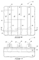
- FIG. 6 is a diagrammatic top plan view of the FIG. 1 semiconductor substrate fragment at a processing step subsequent to that shown by FIG. 5 .
- FIG. 7 is a cross sectional view of the FIG. 6 substrate fragment comprising a planar cross section taken through line 7 - 7 in FIG. 6 .
- FIG. 8 is a cross sectional view of an alternate embodiment substrate fragment to that shown in FIG. 7 .
- FIG. 9 is a cross sectional view of an alternate embodiment substrate fragment to those shown in FIGS. 7 and 8 .
- FIG. 10 is a cross sectional view of an alternate embodiment substrate fragment to those shown in FIG. 7-9 .
- FIG. 11 is a diagrammatic isometric view of a semiconductor substrate fragment in process in accordance with an embodiment of the invention.
- FIG. 12 is a view of the FIG. 11 substrate fragment at a processing step subsequent to that shown by FIG. 11 .
- FIG. 13 is a view of the FIG. 12 substrate fragment at a processing step subsequent to that shown by FIG. 12 .
- FIG. 14 is a view of the FIG. 13 substrate fragment at a processing step subsequent to that shown by FIG. 13 .
- FIG. 15 is a view of the FIG. 14 substrate fragment at a processing step subsequent to that shown by FIG. 14 .
- FIG. 16 is a view of the FIG. 15 substrate fragment at a processing step subsequent to that shown by FIG. 15 .
- FIG. 17 is a view of the FIG. 16 substrate fragment at a processing step subsequent to that shown by FIG. 16 .
- FIG. 18 is a diagrammatic isometric view of a semiconductor substrate fragment in process in accordance with an embodiment of the invention.
- FIG. 19 is a view of the FIG. 18 substrate fragment at a processing step subsequent to that shown by FIG. 18 .
- a substrate for example a semiconductor substrate
- a substrate for example a semiconductor substrate
- semiconductor substrate or “semiconductive substrate” is defined to mean any construction comprising semiconductive material, including, but not limited to, bulk semiconductive materials such as a semiconductive wafer (either alone or in assemblies comprising other materials thereon), and semiconductive material layers (either alone or in assemblies comprising other materials).
- substrate refers to any supporting structure, including, but not limited to, the semiconductive substrates described above.
- Substrate fragment 10 comprises material 12 over which a series of conductive lines 13 , 14 and 15 has been fabricated. Multiple different materials and layers would likely be present at least below material 12 , and may for example comprise bulk semiconductor processing, semiconductor-on-insulator processing, or other substrates in process and whether existing or yet-to-be developed.
- material 12 is insulative, for example doped and/or undoped silicon dioxide. Insulative material 12 is also shown as being received between conductive lines 13 , 14 and 15 .
- Conductive lines 13 , 14 and 15 may be comprised of one or more conductive materials and/or layers, including conductively doped semiconductive material.
- each of conductive lines 13 , 14 and 15 will comprise a first conductive electrode of a memory cell which will be fabricated.
- a plurality of non-volatile resistive oxide memory cells may be fabricated within a memory array, thereby for example perhaps millions of such individual memory cells being fabricated at essentially the same time.
- each of conductive lines 13 , 14 and 15 may constitute a first conductive electrode of multiple different memory cells, as will be apparent in the continuing discussion.
- Conductive lines 13 , 14 and 15 comprise an example of a plurality of one of conductive word lines or conductive bit lines which have been formed over a substrate.
- each of the depicted conductive lines 13 , 14 and 15 will comprise conductive word lines or each of conductive lines 13 , 14 and 15 will comprise conductive bit lines.
- the lines 13 , 14 and 15 run in respective straight lines within the array, although other configurations are of course contemplated.
- a metal oxide-comprising material 18 has been formed over first conductive electrode 15 , and accordingly over the one of conductive word lines 13 , 14 , and 15 or conductive bit lines 13 , 14 , and 15 .
- Material 18 may or may not comprise an outermost planar surface.
- Material 18 may be homogenous or non-homogenous, and may comprise one or more different compositions and/or layers. Accordingly, material 18 may be deposited/formed in one or more steps.
- material 18 might comprise multi-resistive state metal oxide-comprising material, further for example comprising two different layers or regions generally regarded as or understood to be active or passive regions, although not necessarily.
- Example active cell region compositions which comprise metal oxide and can be configured in multi-resistive states include one or a combination of Sr x Ru y O z , Ru x O y , and In x Sn y O z .
- Other examples include MgO, Ta 2 O 5 , SrTiO 3 , ZrO x (perhaps doped with La), and CaMnO 3 (doped with one or more of Pr, La, Sr, or Sm).
- Example passive cell region compositions include one or a combination of Al 2 O 3 , TiO 2 , and HfO 2 .
- multi-resistive state metal oxide-comprising material 28 might comprise additional metal oxide or other materials not comprising metal oxide.
- Example materials and constructions for a multi-resistive state region comprising one or more layers including a programmable metal oxide-comprising material are described and disclosed in U.S. Pat. Nos. 6,753,561; 7,149,108; 7,067,862; and 7,187,201, as well as in U.S. Patent Application Publication Nos. 2006/0171200 and 2007/0173019, the disclosures of which are hereby fully incorporated herein by reference for all purposes of this disclosure.
- multi-resistive state metal oxide-comprising materials encompass filament-type metal oxides, ferroelectric metal oxides and others, and whether existing or yet-to-be developed, as long as resistance of the metal oxide-comprising material can be selectively changed.
- metal oxide-comprising material 18 might be configured to have its current leakage capabilities be selectively varied in addition to or instead of its resistive state.
- etch stop material 20 has been deposited over metal oxide-comprising material 18 .
- etch stop material is homogenous and in one embodiment is completely blanketly covering over metal oxide-comprising material 18 .
- etch stop material 20 will be used to provide an etch stopping function when etching a subsequently deposited conductive material, as will be described below.
- etch stop material 20 comprises an inherently/always electrically conductive material, for example an inherently/always electrically conductive metal oxide.
- inherently/always electrically conductive materials include indium tin oxide, TiN, oxygen doped TiN, and RuO 2 . Accordingly, etch stop material 20 may comprise one or more of such compositions.
- etch stop material 20 is of an electrically insulative composition yet is of an effective thinness in such instances to be electrically conductive through such composition. Composition of etch stop material 20 in such instances will determine maximum thickness of material 20 in a finished circuitry construction to enable electrical conduction through such composition.
- Example electrically insulative compositions for etch stop material 20 comprise at least one of silicon dioxide, silicon nitride, silicon oxynitride, silicon carbide, and titanium dioxide.
- etch stop material 20 has a thickness no greater than 200 Angstroms in a finished circuitry construction incorporating the memory cell or cells being fabricated, and in one embodiment no greater than 100 Angstroms in such finished circuitry construction.
- an example thickness range for etch stop material 20 in a finished circuitry construction incorporating such etch stop material is from 50 Angstroms to 200 Angstroms, although thicknesses less than 50 Angstroms are also of course contemplated.
- Conductive material 22 has been deposited over etch stop material 20 .
- Conductive material 22 may be homogenous or non-homogenous, and regardless be of the same or different composition from that of conductive material of first electrode 15 .
- a plurality of the other of conductive word lines 24 , 25 , 26 or conductive bit lines 24 , 25 , 26 has been formed from conductive material 22 .
- An example technique for forming conductive lines 24 , 25 , and 26 comprises photolithographic patterning of an imageable material, such as photoresist, followed by develop and subsequent subtractive etch of material 22 to produce the FIGS. 6 and 7 construction. Portions of each of lines 24 , 25 , and 26 will comprise second conductive electrodes of the respective memory cells being fabricated.
- the forming of the second conductive electrode 24 , 25 , and 26 of a respective memory cell comprises etching through conductive material 22 to stop etching action relative to etch stop material 20 .
- etch stop material 20 provides an effective etch stopping function when etching through material 22 to form the depicted plurality of the other of conductive word lines 24 , 25 , 26 or conductive bit lines 24 , 25 , 26 .
- FIGS. 6 and 7 depict respective non-volatile resistive oxide memory cells 30 which comprise a portion of conductive line 15 which comprises a first conductive electrode of the respective memory cells, and a second conductive electrode comprising portions of one of the depicted conductive lines 24 , 25 , and 26 .
- the respective memory cells 30 also comprise both metal oxide-comprising material 18 and etch stop material 20 which are received between the respective first and second conductive electrodes of the respective memory cells. Accordingly, etch stop material 20 comprises a part of the finished circuitry construction incorporating an individual memory cell.
- etch stop material 20 is completely blanketly covering between metal oxide-comprising material 18 and the overlying second conductive electrode in a finished circuitry construction incorporating the memory cell.
- etch stop material 20 is of an electrically insulative composition
- such material 20 is of an effective thinness between the respective first and second conductive electrodes to be electrically conductive through such composition when a multi-resistive state metal oxide-comprising material 18 is in a lowest resistive state, thereby for example for a binary memory cell enabling such cell to be switchable between “on” and “off” conditions.
- etch stop material 20 is conductive, such is removed sufficiently (not shown in FIGS. 6 and 7 ) between/among memory cells 30 to preclude electrical shorting of different memory cells 30 .
- etch stop material 20 is insulative, such may or may not need to be any of treated, removed partially, removed wholly, or not removed at all between/among memory cells 30 to preclude electrical shorting of different memory cells 30 . Such may depend at least in part upon the dielectric properties of etch stop material 20 and/or spacing between adjacent memory cells 30 . For example in the embodiment of FIGS.
- composition of an insulative etch stop material 20 might be both (a) insufficiently resistive to enable conductivity between electrodes 22 and 15 when material 18 is in a lowest resistance state due in part to separation distance between electrodes 22 and 15 in a memory cell, and (b) sufficiently resistive between adjacent memory cells 30 due to greater separation distance therebetween as compared to the separation distance between electrodes 22 and 15 in a memory cell. Yet if condition (a) is satisfied and condition (b) is not, etch stop material 20 between memory cells 30 might be one or both of i) treated to increase resistivity thereof, or ii) thinned.
- Such might be desirable to minimize electrical interference between or among spaced memory cells 30 , and further may be desirable even if both conditions (a) and (b) are satisfied.
- segments of etch stop material 20 remaining between adjacent memory cells 30 might adversely or unpredictably impact programming voltage required to change states of material 18 in spaced memory cells 30 .
- Thinning and/or treating to increase resistance of such material 20 between memory cells 30 might be used in such instances.
- different dielectric materials 20 can be deposited in one lower resistance state and treated after deposition to a second higher resistance state.
- lower density of a given inherently/always dielectric material typically results in lower resistivity as compared to higher density of the same material.
- a low density silicon dioxide can be increased in density and resistance by treating with ozone with deionized water at elevated temperature.
- etch stop material 20 can be removed to material 18 between memory cells 30 such that material 20 does not interconnect among individual memory cells 30 .
- the act of etching through conductive material 22 to form the respective second conductive electrode portions of the memory cell stops on etch stop material 20 such that no detectable quantity of etch stop material 20 is etched during any of the etching of such conductive material 22 .
- FIG. 7 depicts a perfect selective etch of material 22 relative to etch stop material 20 such that none of etch stop material 20 is etched away after clearing conductive material 22 from between the depicted other of conductive word lines 24 , 25 , 26 or conductive bit lines 24 , 25 , 26 .
- an alternate embodiment comprises etching through conductive material 22 whereby etch stop material 20 is only partially etched into upon complete etching through material 22 between conductive lines 24 , 25 , and 26 , and accordingly still providing an etch stopping function during the etch of conductive material 22 .
- Such partial etching into etch stop material 20 while etching conductive material 22 might, for example, etch less or more than half of thickness of etch stop material 20 , or about half of thickness of etch stop material 20 .
- FIG. 8 illustrates an alternate embodiment substrate fragment 10 a wherein etching of conductive material 22 has also etched partially into etch stop material 20 to less than half of the thickness of etch stop material 20 .
- FIG. 8 illustrates an alternate embodiment substrate fragment 10 a wherein etching of conductive material 22 has also etched partially into etch stop material 20 to less than half of the thickness of etch stop material 20 .
- FIG. 9 illustrates an alternate embodiment substrate fragment 10 b wherein etching through conductive material 22 has etched partially into etch stop material 20 to more than half of the thickness etch stop material 20 .
- any etching of etch stop material 20 while etching conductive material 22 may or may not result in some lateral recess of material 22 relative to one or both of the respective first and second conductive electrodes, whereby the etch stop material may not be completely blanketly covering between the metal oxide-comprising material and the second conductive electrode in a finished circuitry construction incorporating the memory cell.
- subsequently deposited insulative and wiring layers would likely be provided over each of the substrates of FIGS. 7, 8, and 9 in respective finished circuitry constructions.
- methods of forming a non-volatile resistive oxide memory cell and/or memory array are void of exposing any of metal oxide-comprising material 18 to any etching plasma, for example as may be desirable to overcome one or more problems identified in the Background section above.
- metal oxide-comprising material 18 may be exposed to an etching plasma.
- some embodiments of the invention also contemplate etching through etch stop material 20 laterally outward of the second conductive electrode to the metal oxide-comprising material after etching through the conductive material and using the etch stopping attribute or act relative to the etch stop material. For example, FIG.
- substrate fragment 10 c illustrates an alternate embodiment substrate fragment 10 c which could result from subsequent processing of any of the substrate fragments 10 , 10 a , or 10 b of FIGS. 7, 8, and 9 , respectively.
- Substrate fragment 10 c in FIG. 10 has been processed to etch through etch stop material 20 laterally outward of each of the depicted second conductive electrodes 24 , 25 , and 26 to metal oxide-comprising material 18 .
- Such subsequent etching of etch stop material 20 may or may not be conducted selectively relative to metal oxide-comprising material 18 , and may or may not comprise wet, dry, and/or plasma etching.
- programmable junctions or memory cells manifest where the respective word lines and bit lines cross one another.
- the plurality of the other of conductive word lines 24 , 25 , 26 or conductive bit lines 24 , 25 , 26 run generally parallel an outer major surface of the substrate (as do the plurality of one of conductive word lines 13 , 14 , 15 or conductive bit lines 13 , 14 , 15 ), and are angled relative to the plurality of such one of word lines 13 , 14 , 15 or bit lines 13 , 14 , 15 .
- the outermost surface of the respective substrates may or may not be planar at certain or any points during processing.
- the above-described and depicted substrates at their respective largest or global scales can be considered as having some respective outer major surface that can be considered, on average, as defining some general horizontal plane relative to which the various layers and circuitry components are fabricated.
- Such outer major surface of the respective substrates may, of course, be comprised of more than one composition at different points in processing of the respective substrates.
- the outer major surface of the respective substrates can be considered as averaging to be planar throughout fabrication, with such general plane rising and lowering as the circuitry is fabricated.
- a substrate fragment is indicated generally with reference numeral 40 .
- Such comprises material 42 relative to which a series of conductive lines has been fabricated, for example lines 44 and 46 .
- material 42 is insulative, for example doped and/or undoped silicon dioxide. Insulative material 42 is also shown as being received between conductive lines 44 and 46 .
- Conductive lines 44 and 46 may be comprised of one or more conductive materials and/or layers, including conductively doped semiconductive material.
- each of conductive lines 44 and 46 will comprise a first conductive electrode of a respective memory cell which will be fabricated.
- a plurality of non-volatile resistive oxide memory cells may be fabricated within a memory array, thereby for example perhaps millions of such individual memory cells being fabricated at essentially the same time.
- each of conductive lines 44 and 46 may constitute a first conductive electrode of multiple different memory cells.
- Conductive lines 44 and 46 comprise an example of a plurality of one of conductive word lines or conductive bit lines which have been formed over a substrate.
- each of the depicted conductive lines 44 and 46 will comprise conductive word lines or each of conductive lines 44 and 46 will comprise conductive bit lines.
- lines 44 and 46 run in respective straight lines within the array, although other configurations are of course contemplated.
- Metal oxide-comprising material 48 has been formed over the one of conductive word lines 44 , 46 or conductive bit lines 44 , 46 .
- Example materials and constructions are as described above in the first-described embodiments with respect to material 18 .
- Etch stop material 50 has been deposited over metal oxide-comprising material 48 .
- Example compositions and constructions are as described above in the first-described embodiments in connection with etch stop material 20 . However, none or some of etch stop material 20 may remain in a finished circuitry construction of a non-volatile resistive oxide memory cell in the embodiments of FIGS. 11-19 , as will be apparent from the continuing discussion.
- Damascene template material 52 has been deposited over etch stop material 50 .
- example damascene template materials include at least one of amorphous carbon, transparent carbon, photoresist, silicon nitride, silicon dioxide (whether doped or undoped and including silicate glasses) and polysilicon (whether doped or undoped).
- a series of elongated trenches 60 , 62 has been etched into damascene template material 52 to etch stop material 50 over the plurality of the one of word lines 44 , 46 or bit lines 44 , 46 to stop relative to etch stop material 50 .
- either of trenches 60 , 62 might be considered as an opening which has been etched through damascene template material 52 to etch stop material 50 over a first conductive electrode comprised of a portion of either of conductive lines 44 , 46 to stop relative to etch stop material 50 .
- such example openings respectively comprise an elongated trench in the damascene template material which runs generally parallel an outer major surface of the substrate, and which is angled relative to the plurality of the one of word lines 44 , 46 or bit lines 44 , 46 .
- Some of etch stop material 50 might also be etched into while still providing an etch stopping function.
- etching has been conducted through etch stop material 50 within the respective openings 60 , 62 to metal oxide-comprising material 48 .
- Any suitable wet or dry etching chemistry might be utilized. In one embodiment, such etching does not utilize any etching plasma such that the process is void of exposing metal oxide-comprising material 50 within the respective openings 60 , 62 to any etching plasma, for example to overcome one or more of the problems identified in the Background section above.
- the etch stop material comprises silicon dioxide
- a suitable dry non-plasma etching chemistry comprises use of NH 3 and HF vapors, and/or NF 3 radicals.
- ion implanting of a suitable substance might be conducted into etch stop material 50 within the respective opening 60 , 62 , or even before deposition of damascene template material 52 , to facilitate ease of etching of etch stop material 50 from within the respective openings 60 , 62 .
- etching of etch stop material 50 within openings 60 , 62 may or may not recess material 50 laterally beneath damascene template material 52 . If such lateral recessing occurs and produces a less than desirable resultant outline, subsequent etching might be conducted at least of the sidewalls of damascene template material 52 to remove or reduce such recesses.
- FIGS. 14 and 15 depict an example embodiment whereby conductive material 64 has been deposited to overfill the respective openings/trenches 60 , 62 , and then polished back to at least an outermost surface of damascene template material 52 .
- a plurality of the other of conductive word lines 70 , 72 ( FIG. 16 ) or conductive bit lines 70 , 72 has been formed from conductive material 64 .
- damascene template material 52 may remain as part of the finished circuitry construction where such is of a desired insulative material. Alternately and by way of example only and referring to FIG. 16 , all remaining of damascene template material 52 (not shown) has been removed from the substrate.
- etch stop material 50 may be removed from the substrate, with FIG. 17 showing an example embodiment wherein all such remaining etch stop material 50 (not shown) has been removed from the substrate.
- metal oxide-comprising material 48 between the one of word lines 44 , 46 or bit lines 44 , 46 and the other of word lines 70 , 72 or bit lines 70 , 72 form individually programmable junctions where the word lines and bit lines cross one another, thereby forming the depicted example individual non-volatile resistive oxide memory cells 75 .
- the above-described embodiments depict non-volatile resistive oxide memory cells and memory arrays where word lines and bit lines cross one another without isolation patterning of the metal oxide-comprising material and without a conductive projection extending from one or both of the word lines or bit lines for each memory cell.
- embodiments of the invention encompass incorporating these or other features in a memory cell or an array of memory cells.
- the metal oxide-comprising material might be patterned relative to one or a plurality of memory cells, and/or one or more conductive projections might be provided relative to the respective word lines and/or bit lines.
- FIGS. 18 and 19 depict an alternate exemplary embodiment with respect to a substrate fragment 40 a .
- Like numerals from the FIGS. 11-17 embodiment have been utilized where appropriate, with differences being indicated with the suffix “a” or with different numerals.
- FIG. 18 corresponds in processing sequence to FIG. 11 of the substrate fragment embodiment of FIG. 11 , yet wherein a plurality of respective conductive projections 80 extend upwardly from word lines 44 , 46 or bit lines 44 , 46 .
- a plurality of respective conductive projections 80 extend upwardly from word lines 44 , 46 or bit lines 44 , 46 .
- Such conductive projection extending upwardly from a conductive line 44 , 46 may be of the same or different composition from that of the conductive line.
- conductive lines 44 , 46 and respective projections 80 are depicted as being of the same composition, and may comprise one or more conductive materials including conductively doped semiconductive material.
- An example manner of fabricating conductive lines 44 , 46 to include projections 80 includes initial deposition of one or more conductive materials to a thickness at or greater than the thickness of a conductive projection including that of the underlying conductive line. The outline of the conductive lines can then be patterned. This can be followed by cross patterning of the conductive projections using a timed etch into the conductive material from which such projections and lines are formed. Other manners of fabrication might be used.
- FIG. 19 depicts an analogous construction to that of FIG. 17 but additionally incorporating projections 80 to thereby form individual non-volatile resistive oxide memory cells 75 a . Nevertheless and regardless, such still defines or forms a non-volatile resistive oxide memory array comprising metal oxide-comprising material received between the one of the word lines or bit lines and the other of the word lines or bit lines to form individually programmable junctions where the word lines and bit lines cross one another.
- downward projections might be provided from the overlying conductive lines 70 , 72 .
- either or both of such projection concepts and/or isolation patterning of metal oxide-comprising material might be incorporated in any of the above-described FIGS. 1-10 embodiments.
Abstract
Description
Claims (33)
Priority Applications (2)
| Application Number | Priority Date | Filing Date | Title |
|---|---|---|---|
| US12/166,604 US9343665B2 (en) | 2008-07-02 | 2008-07-02 | Methods of forming a non-volatile resistive oxide memory cell and methods of forming a non-volatile resistive oxide memory array |
| US15/156,105 US9666801B2 (en) | 2008-07-02 | 2016-05-16 | Methods of forming a non-volatile resistive oxide memory cell and methods of forming a non-volatile resistive oxide memory array |
Applications Claiming Priority (1)
| Application Number | Priority Date | Filing Date | Title |
|---|---|---|---|
| US12/166,604 US9343665B2 (en) | 2008-07-02 | 2008-07-02 | Methods of forming a non-volatile resistive oxide memory cell and methods of forming a non-volatile resistive oxide memory array |
Related Child Applications (1)
| Application Number | Title | Priority Date | Filing Date |
|---|---|---|---|
| US15/156,105 Division US9666801B2 (en) | 2008-07-02 | 2016-05-16 | Methods of forming a non-volatile resistive oxide memory cell and methods of forming a non-volatile resistive oxide memory array |
Publications (2)
| Publication Number | Publication Date |
|---|---|
| US20100003782A1 US20100003782A1 (en) | 2010-01-07 |
| US9343665B2 true US9343665B2 (en) | 2016-05-17 |
Family
ID=41464699
Family Applications (2)
| Application Number | Title | Priority Date | Filing Date |
|---|---|---|---|
| US12/166,604 Active 2029-02-12 US9343665B2 (en) | 2008-07-02 | 2008-07-02 | Methods of forming a non-volatile resistive oxide memory cell and methods of forming a non-volatile resistive oxide memory array |
| US15/156,105 Active US9666801B2 (en) | 2008-07-02 | 2016-05-16 | Methods of forming a non-volatile resistive oxide memory cell and methods of forming a non-volatile resistive oxide memory array |
Family Applications After (1)
| Application Number | Title | Priority Date | Filing Date |
|---|---|---|---|
| US15/156,105 Active US9666801B2 (en) | 2008-07-02 | 2016-05-16 | Methods of forming a non-volatile resistive oxide memory cell and methods of forming a non-volatile resistive oxide memory array |
Country Status (1)
| Country | Link |
|---|---|
| US (2) | US9343665B2 (en) |
Cited By (2)
| Publication number | Priority date | Publication date | Assignee | Title |
|---|---|---|---|---|
| TWI732723B (en) * | 2020-02-12 | 2021-07-01 | 力旺電子股份有限公司 | Resistive random-access memory cell and associated array structure |
| TWI785861B (en) * | 2020-12-18 | 2022-12-01 | 力旺電子股份有限公司 | Resistive memory cell and associated cell array structure |
Families Citing this family (23)
| Publication number | Priority date | Publication date | Assignee | Title |
|---|---|---|---|---|
| US7768812B2 (en) | 2008-01-15 | 2010-08-03 | Micron Technology, Inc. | Memory cells, memory cell programming methods, memory cell reading methods, memory cell operating methods, and memory devices |
| US8034655B2 (en) | 2008-04-08 | 2011-10-11 | Micron Technology, Inc. | Non-volatile resistive oxide memory cells, non-volatile resistive oxide memory arrays, and methods of forming non-volatile resistive oxide memory cells and memory arrays |
| US8211743B2 (en) * | 2008-05-02 | 2012-07-03 | Micron Technology, Inc. | Methods of forming non-volatile memory cells having multi-resistive state material between conductive electrodes |
| US8114468B2 (en) | 2008-06-18 | 2012-02-14 | Boise Technology, Inc. | Methods of forming a non-volatile resistive oxide memory array |
| US8134137B2 (en) | 2008-06-18 | 2012-03-13 | Micron Technology, Inc. | Memory device constructions, memory cell forming methods, and semiconductor construction forming methods |
| US9343665B2 (en) | 2008-07-02 | 2016-05-17 | Micron Technology, Inc. | Methods of forming a non-volatile resistive oxide memory cell and methods of forming a non-volatile resistive oxide memory array |
| US8411477B2 (en) | 2010-04-22 | 2013-04-02 | Micron Technology, Inc. | Arrays of vertically stacked tiers of non-volatile cross point memory cells, methods of forming arrays of vertically stacked tiers of non-volatile cross point memory cells, and methods of reading a data value stored by an array of vertically stacked tiers of non-volatile cross point memory cells |
| US8427859B2 (en) | 2010-04-22 | 2013-04-23 | Micron Technology, Inc. | Arrays of vertically stacked tiers of non-volatile cross point memory cells, methods of forming arrays of vertically stacked tiers of non-volatile cross point memory cells, and methods of reading a data value stored by an array of vertically stacked tiers of non-volatile cross point memory cells |
| US8283198B2 (en) * | 2010-05-10 | 2012-10-09 | Micron Technology, Inc. | Resistive memory and methods of processing resistive memory |
| US8289763B2 (en) | 2010-06-07 | 2012-10-16 | Micron Technology, Inc. | Memory arrays |
| KR101133701B1 (en) * | 2010-09-10 | 2012-04-06 | 주식회사 하이닉스반도체 | Method for manufacturing semiconductor device with buried bitline |
| US8351242B2 (en) | 2010-09-29 | 2013-01-08 | Micron Technology, Inc. | Electronic devices, memory devices and memory arrays |
| US8759809B2 (en) | 2010-10-21 | 2014-06-24 | Micron Technology, Inc. | Integrated circuitry comprising nonvolatile memory cells having platelike electrode and ion conductive material layer |
| US8526213B2 (en) | 2010-11-01 | 2013-09-03 | Micron Technology, Inc. | Memory cells, methods of programming memory cells, and methods of forming memory cells |
| US8796661B2 (en) | 2010-11-01 | 2014-08-05 | Micron Technology, Inc. | Nonvolatile memory cells and methods of forming nonvolatile memory cell |
| US9454997B2 (en) | 2010-12-02 | 2016-09-27 | Micron Technology, Inc. | Array of nonvolatile memory cells having at least five memory cells per unit cell, having a plurality of the unit cells which individually comprise three elevational regions of programmable material, and/or having a continuous volume having a combination of a plurality of vertically oriented memory cells and a plurality of horizontally oriented memory cells; array of vertically stacked tiers of nonvolatile memory cells |
| US8431458B2 (en) | 2010-12-27 | 2013-04-30 | Micron Technology, Inc. | Methods of forming a nonvolatile memory cell and methods of forming an array of nonvolatile memory cells |
| US8791447B2 (en) | 2011-01-20 | 2014-07-29 | Micron Technology, Inc. | Arrays of nonvolatile memory cells and methods of forming arrays of nonvolatile memory cells |
| US8488365B2 (en) | 2011-02-24 | 2013-07-16 | Micron Technology, Inc. | Memory cells |
| US8537592B2 (en) | 2011-04-15 | 2013-09-17 | Micron Technology, Inc. | Arrays of nonvolatile memory cells and methods of forming arrays of nonvolatile memory cells |
| KR102043920B1 (en) * | 2011-11-08 | 2019-11-12 | 노스이스턴 유니버시티 | Damascene template for directed assembly and transfer of nanoelements |
| EP3580375A4 (en) | 2017-02-10 | 2020-12-02 | Northeastern University | Damascene template for nanoelement printing fabricated without chemomechanical planarizaton |
| US11114331B2 (en) * | 2019-05-03 | 2021-09-07 | United Microelectronics Corp. | Method for fabricating shallow trench isolation |
Citations (268)
| Publication number | Priority date | Publication date | Assignee | Title |
|---|---|---|---|---|
| GB1266513A (en) | 1969-05-19 | 1972-03-08 | ||
| US4715685A (en) | 1985-03-04 | 1987-12-29 | Energy Conversion Devices, Inc. | Liquid crystal display having potential source in a diode ring |
| US4964080A (en) | 1990-03-09 | 1990-10-16 | Intel Corporation | Three-dimensional memory cell with integral select transistor |
| US5049970A (en) | 1987-11-17 | 1991-09-17 | Sharp Kabushiki Kaisha | High resistive element |
| US5122476A (en) | 1991-01-28 | 1992-06-16 | Micron Technology, Inc. | Double DRAM cell |
| US6034882A (en) | 1998-11-16 | 2000-03-07 | Matrix Semiconductor, Inc. | Vertically stacked field programmable nonvolatile memory and method of fabrication |
| US6218696B1 (en) | 1999-06-07 | 2001-04-17 | Infineon Technologies North America Corp. | Layout and wiring scheme for memory cells with vertical transistors |
| US20020018355A1 (en) | 1998-11-16 | 2002-02-14 | Johnson Mark G. | Vertically stacked field programmable nonvolatile memory and method of fabrication |
| US20020034117A1 (en) | 2000-09-19 | 2002-03-21 | Takeshi Okazawa | Non-volatile semiconductor memory device with magnetic memory cell array |
| US20020079524A1 (en) | 2000-12-26 | 2002-06-27 | Charles Dennison | Lower electrode isolation in a double-wide trench |
| US6432767B2 (en) * | 1995-12-05 | 2002-08-13 | Hitachi, Ltd. | Method of fabricating semiconductor device |
| US20020196695A1 (en) | 2001-05-30 | 2002-12-26 | Stmicroelectronics S.R.L. | Column multiplexer for semiconductor memories |
| US20030031047A1 (en) | 2001-08-09 | 2003-02-13 | Anthony Thomas C. | One-time programmable unit memory cell based on vertically oriented fuse and diode and one-time programmable memory using the same |
| US6524867B2 (en) | 2000-12-28 | 2003-02-25 | Micron Technology, Inc. | Method for forming platinum-rhodium stack as an oxygen barrier |
| US20030086313A1 (en) | 2001-11-07 | 2003-05-08 | Yoshiaki Asao | Magnetic memory device using SOI substrate and method of manufacturing the same |
| KR20030048421A (en) | 2000-11-01 | 2003-06-19 | 가가쿠 기쥬츠 신코 지교단 | Point contact array, not circuit, and electronic circuit comprising the same |
| US20030174570A1 (en) | 2002-03-12 | 2003-09-18 | Mitsubishi Denki Kabushiki Kaisha | Semiconductor memory device having potential control circuit |
| US20030185049A1 (en) | 2002-04-02 | 2003-10-02 | Peter Fricke | Cubic memory array |
| US20030218929A1 (en) | 2002-05-24 | 2003-11-27 | Heiko Fibranz | Circuit configuration having a flow controller, integrated memory device, and test configuration having such a circuit configuration |
| US20030218902A1 (en) | 2002-05-22 | 2003-11-27 | Perner Frederick A. | Triple sample sensing for magnetic random access memory (MRAM) with series diodes |
| US20030223283A1 (en) | 2002-04-03 | 2003-12-04 | Mitsubishi Denki Kabushiki Kaisha | Magnetic memory device |
| US20040002186A1 (en) | 2002-06-27 | 2004-01-01 | Vyvoda Michael A. | Electrically isolated pillars in active devices |
| US6693821B2 (en) | 2001-06-28 | 2004-02-17 | Sharp Laboratories Of America, Inc. | Low cross-talk electrically programmable resistance cross point memory |
| US20040100835A1 (en) | 2002-11-27 | 2004-05-27 | Nec Corporation | Magnetic memory cell and magnetic random access memory using the same |
| US20040108528A1 (en) | 2001-06-28 | 2004-06-10 | Sharp Laboratories Of America, Inc. | Cross-point resistor memory array and method of fabrication |
| US6753562B1 (en) | 2003-03-27 | 2004-06-22 | Sharp Laboratories Of America, Inc. | Spin transistor magnetic random access memory device |
| US6753561B1 (en) | 2002-08-02 | 2004-06-22 | Unity Semiconductor Corporation | Cross point memory array using multiple thin films |
| US20040124407A1 (en) | 2000-02-11 | 2004-07-01 | Kozicki Michael N. | Scalable programmable structure, an array including the structure, and methods of forming the same |
| US6778421B2 (en) | 2002-03-14 | 2004-08-17 | Hewlett-Packard Development Company, Lp. | Memory device array having a pair of magnetic bits sharing a common conductor line |
| US6785159B2 (en) * | 2002-08-29 | 2004-08-31 | Micron Technology, Inc. | Combination etch stop and in situ resistor in a magnetoresistive memory and methods for fabricating same |
| US20040188714A1 (en) | 2003-03-31 | 2004-09-30 | Scheuerlein Roy E. | Three-dimensional memory device incorporating segmented bit line memory array |
| US6806531B1 (en) | 2003-04-07 | 2004-10-19 | Silicon Storage Technology, Inc. | Non-volatile floating gate memory cell with floating gates formed in cavities, and array thereof, and method of formation |
| US20040245547A1 (en) | 2003-06-03 | 2004-12-09 | Hitachi Global Storage Technologies B.V. | Ultra low-cost solid-state memory |
| US6834008B2 (en) | 2002-08-02 | 2004-12-21 | Unity Semiconductor Corporation | Cross point memory array using multiple modes of operation |
| US20050001257A1 (en) | 2003-02-14 | 2005-01-06 | Till Schloesser | Method of fabricating and architecture for vertical transistor cells and transistor-controlled memory cells |
| KR20050008353A (en) | 2003-07-15 | 2005-01-21 | 현대자동차주식회사 | Knocking sensor mounting position determining method |
| US20050032100A1 (en) | 2003-06-24 | 2005-02-10 | California Institute Of Technology | Electrochemical method and resulting structures for attaching molecular and biomolecular structures to semiconductor micro and nanostructures |
| US20050054119A1 (en) * | 2003-09-05 | 2005-03-10 | Sharp Laboratories Of America, Inc. | Buffered-layer memory cell |
| US20050128799A1 (en) | 2003-12-05 | 2005-06-16 | Renesas Technology Corp. | Semiconductor integrated circuit device |
| JP2005175457A (en) | 2003-12-08 | 2005-06-30 | Sharp Corp | Rram memory cell electrode |
| US20050161747A1 (en) | 2004-01-26 | 2005-07-28 | Hsiang-Lan Lung | Thin film phase-change memory |
| US20050174835A1 (en) | 2004-02-06 | 2005-08-11 | Unity Semiconductor Corporation | Multi-resistive state element with reactive metal |
| US6930324B2 (en) | 2002-12-31 | 2005-08-16 | Infineon Technologies Ag | Device architecture and process for improved vertical memory arrays |
| US6940113B2 (en) | 2001-06-28 | 2005-09-06 | Sharp Laboratories Of America, Inc. | Trench isolated cross-point memory array |
| US6946702B2 (en) | 2003-06-03 | 2005-09-20 | Winbond Electronics Corp. | Resistance random access memory |
| US20050205943A1 (en) | 2004-03-17 | 2005-09-22 | Sanyo Electric Co., Ltd. | Memory and method of fabricating the same |
| US6950369B2 (en) | 2001-02-06 | 2005-09-27 | Mitsubishi Denki Kabushiki Kaisha | Magnetic memory device capable of passing bidirectional currents through the bit lines |
| US6955992B2 (en) | 2003-09-30 | 2005-10-18 | Sharp Laboratories Of America, Inc. | One mask PT/PCMO/PT stack etching process for RRAM applications |
| US6958273B2 (en) | 2003-03-21 | 2005-10-25 | Silicon Storage Technology, Inc. | Self-aligned method of forming a semiconductor memory array of floating gate memory cells with buried floating gate, pointed floating gate and pointed channel region, and a memory array made thereby |
| US6961258B2 (en) | 2001-06-30 | 2005-11-01 | Ovonyx, Inc. | Pore structure for programmable device |
| US20050250281A1 (en) | 2004-04-26 | 2005-11-10 | Infineon Technologies Ag | Method for manufacturing resistively switching memory devices |
| US6970375B2 (en) | 2002-08-02 | 2005-11-29 | Unity Semiconductor Corporation | Providing a reference voltage to a cross point memory array |
| US20050275003A1 (en) | 2004-06-10 | 2005-12-15 | Sharp Kabushiki Kaisha | Crosspoint structure semiconductor memory device, and manufacturing method thereof |
| US20050287741A1 (en) | 2004-06-28 | 2005-12-29 | Yi Ding | Nonvolatile memory fabrication methods in which a dielectric layer underlying a floating gate layer is spaced from an edge of an isolation trench and/or an edge of the floating gate layer |
| US6985374B2 (en) | 2003-01-17 | 2006-01-10 | Seiko Epson Corporation | Ferroelectric memory device |
| WO2006003620A1 (en) | 2004-06-30 | 2006-01-12 | Koninklijke Philips Electronics N.V. | Method for manufacturing an electric device with a layer of conductive material contacted by nanowire |
| JP2006032729A (en) | 2004-07-16 | 2006-02-02 | Matsushita Electric Ind Co Ltd | Nonvolatile memory and its manufacturing method |
| JP2006040981A (en) | 2004-07-22 | 2006-02-09 | Sharp Corp | High density soi crosspoint memory array and its manufacturing method |
| US20060035451A1 (en) | 2003-05-20 | 2006-02-16 | Sharp Laboratories Of America, Inc. | High-density SOI cross-point memory fabricating method |
| US7002197B2 (en) | 2004-01-23 | 2006-02-21 | Hewlett-Packard Development Company, L.P. | Cross point resistive memory array |
| US7005350B2 (en) | 2002-12-31 | 2006-02-28 | Matrix Semiconductor, Inc. | Method for fabricating programmable memory array structures incorporating series-connected transistor strings |
| US20060046509A1 (en) | 2004-08-31 | 2006-03-02 | Samsung Electronics Co., Ltd. | Method of forming a phase change memory device having a small area of contact |
| US7009278B2 (en) | 2003-11-24 | 2006-03-07 | Sharp Laboratories Of America, Inc. | 3d rram |
| US20060062049A1 (en) | 2004-09-17 | 2006-03-23 | Seok-Heon Lee | Methods for programming user data and confirmation information in nonvolatile memory devices |
| US20060071272A1 (en) * | 2004-10-01 | 2006-04-06 | International Business Machines Corporation | Programmable non-volatile resistance switching device |
| US7029925B2 (en) * | 2002-01-31 | 2006-04-18 | Texas Instruments Incorporated | FeRAM capacitor stack etch |
| US7035141B1 (en) | 2004-11-17 | 2006-04-25 | Spansion Llc | Diode array architecture for addressing nanoscale resistive memory arrays |
| US20060097238A1 (en) | 2002-07-26 | 2006-05-11 | Laurent Breuil | Non-volatile memory element and production method thereof and storage memory arrangement |
| US20060099813A1 (en) | 2004-10-21 | 2006-05-11 | Sharp Laboratories Of America, Inc. | Chemical mechanical polish of PCMO thin films for RRAM applications |
| US7046550B1 (en) | 2005-01-18 | 2006-05-16 | International Business Machines Corporation | Cross-point memory architecture with improved selectivity |
| US7050316B1 (en) | 2004-03-09 | 2006-05-23 | Silicon Storage Technology, Inc. | Differential non-volatile content addressable memory cell and array using phase changing resistor storage elements |
| US20060110878A1 (en) | 2004-11-22 | 2006-05-25 | Macronix International Co., Ltd. | Side wall active pin memory and manufacturing method |
| US7067862B2 (en) | 2002-08-02 | 2006-06-27 | Unity Semiconductor Corporation | Conductive memory device with conductive oxide electrodes |
| US20060160304A1 (en) | 2005-01-19 | 2006-07-20 | Sharp Laboratories Of America, Inc. | Non-volatile memory resistor cell with nanotip electrode |
| KR20060087882A (en) | 2005-01-31 | 2006-08-03 | 삼성전자주식회사 | Nonvolatile memory device using resistance material and fabrication method of the same |
| US20060171200A1 (en) | 2004-02-06 | 2006-08-03 | Unity Semiconductor Corporation | Memory using mixed valence conductive oxides |
| US20060181920A1 (en) | 2005-02-09 | 2006-08-17 | Klaus-Dieter Ufert | Resistive memory element with shortened erase time |
| US20060215445A1 (en) * | 2005-03-28 | 2006-09-28 | In-Gyu Baek | Magneto-resistive memory cells and devices having asymmetrical contacts and methods of fabrication therefor |
| US20060258089A1 (en) | 2005-05-10 | 2006-11-16 | Chen Chung-Zen | FLASH memory device and method of manufacture |
| US7149108B2 (en) | 2002-08-02 | 2006-12-12 | Unity Semiconductor Corporation | Memory array of a non-volatile RAM |
| US20060284242A1 (en) | 2005-06-07 | 2006-12-21 | Jo Sang-Youn | Non-volatile memory device having floating gate and methods forming the same |
| US20060286709A1 (en) | 2005-06-17 | 2006-12-21 | Macronix International Co., Ltd. | Manufacturing methods for thin film fuse phase change ram |
| US20070010082A1 (en) | 2005-07-05 | 2007-01-11 | Cay-Uwe Pinnow | Structure and method for manufacturing phase change memories with particular switching characteristics |
| US20070015330A1 (en) | 2005-07-18 | 2007-01-18 | Sharp Laboratories Of America, Inc. | Metal/semiconductor/metal (MSM) back-to-back Schottky diode |
| US7167387B2 (en) | 2003-10-23 | 2007-01-23 | Matsushita Electric Industrial Co., Ltd. | Variable resistance element, method of manufacturing the element, memory containing the element, and method of driving the memory |
| US20070019923A1 (en) * | 2005-07-22 | 2007-01-25 | Teruo Sasagawa | Support structure for MEMS device and methods therefor |
| US20070034848A1 (en) | 2005-08-15 | 2007-02-15 | Micron Technology, Inc. | Reproducible resistance variable insulating memory devices and methods for forming same |
| US7180160B2 (en) | 2004-07-30 | 2007-02-20 | Infineon Technologies Ag | MRAM storage device |
| US20070041235A1 (en) * | 2005-08-17 | 2007-02-22 | Sharp Kabushiki Kaisha | Semiconductor storage device |
| US20070045615A1 (en) | 2005-08-31 | 2007-03-01 | Samsung Electronics Co., Ltd. | Non-volatile organic resistance random access memory device and method of manufacturing the same |
| US20070048990A1 (en) | 2005-08-30 | 2007-03-01 | Sharp Laboratories Of America, Inc. | Method of buffer layer formation for RRAM thin film deposition |
| US7187201B1 (en) | 2004-06-24 | 2007-03-06 | Xilinx, Inc. | Programmable logic device suitable for implementation in molecular electronics |
| US7193267B2 (en) | 2001-06-28 | 2007-03-20 | Sharp Laboratories Of America, Inc. | Cross-point resistor memory array |
| US20070086235A1 (en) | 2005-10-18 | 2007-04-19 | Du-Eung Kim | Phase-change memory device and method of fabricating the same |
| US20070109835A1 (en) | 2005-11-17 | 2007-05-17 | Sharp Laboratories Of America, Inc. | Cross-point RRAM memory array having low bit line crosstalk |
| US20070121369A1 (en) | 2004-05-27 | 2007-05-31 | Thomas Happ | Resistive memory cell arrangement and a semiconductor memory including the same |
| US20070123039A1 (en) | 2004-11-03 | 2007-05-31 | Elkins Patricia C | Electroless plating of metal caps for chalcogenide-based memory devices |
| US20070120124A1 (en) | 2005-11-30 | 2007-05-31 | I-Wei Chen | Resistance-switching oxide thin film devices |
| US20070132049A1 (en) | 2005-12-12 | 2007-06-14 | Stipe Barry C | Unipolar resistance random access memory (RRAM) device and vertically stacked architecture |
| US20070165434A1 (en) | 2006-01-19 | 2007-07-19 | Samsung Electronics Co., Ltd. | Resistive RAM having at least one varistor and methods of operating the same |
| US7247876B2 (en) | 2000-06-30 | 2007-07-24 | Intel Corporation | Three dimensional programmable device and method for fabricating the same |
| CN101005113A (en) | 2005-12-27 | 2007-07-25 | 旺宏电子股份有限公司 | Method for forming self-aligned thermal isolation cell for a variable resistance memory array |
| US20070173019A1 (en) | 2006-01-09 | 2007-07-26 | Macronix International Co., Ltd. | Programmable Resistive Ram and Manufacturing Method |
| US20070171706A1 (en) | 2006-01-25 | 2007-07-26 | Elpida Memory, Inc. | Semiconductor memory device |
| US20070176261A1 (en) | 2006-01-30 | 2007-08-02 | Macronix International Co., Ltd. | Vertical Side Wall Active Pin Structures in a Phase Change Memory and Manufacturing Methods |
| US20070210348A1 (en) | 2005-12-23 | 2007-09-13 | Song Jongheui | Phase-change memory device and methods of fabricating the same |
| US7273791B2 (en) | 2000-11-09 | 2007-09-25 | Micron Technology, Inc. | Methods for forming a conductive structure using oxygen diffusion through one metal layer to oxidize a second metal layer |
| US20070224770A1 (en) | 2006-03-25 | 2007-09-27 | Makoto Nagashima | Systems and methods for fabricating self-aligned memory cell |
| US20070231988A1 (en) | 2006-03-09 | 2007-10-04 | Samsung Electronics Co., Ltd. | Method of fabricating nanowire memory device and system of controlling nanowire formation used in the same |
| CN101051670A (en) | 2007-04-19 | 2007-10-10 | 复旦大学 | Preparing method for RRAM to avoid forming phenomenon using CuxO as storage medium |
| US20070246795A1 (en) | 2006-04-20 | 2007-10-25 | Micron Technology, Inc. | Dual depth shallow trench isolation and methods to form same |
| US20070257257A1 (en) | 2006-02-20 | 2007-11-08 | Samsung Electronics Co., Ltd. | Nonvolatile memory device including amorphous alloy metal oxide layer and method of manufacturing the same |
| US20070269683A1 (en) | 2005-11-30 | 2007-11-22 | The Trustees Of The University Of Pennyslvani | Non-volatile resistance-switching oxide thin film devices |
| US20070267675A1 (en) * | 2006-05-19 | 2007-11-22 | Samsung Electronics Co., Ltd. | Nonvolatile memory devices including oxygen-deficient metal oxide layers and methods of manufacturing the same |
| US20070268739A1 (en) | 2006-03-08 | 2007-11-22 | Samsung Electronics Co., Ltd. | Nanowire memory device and method of manufacturing the same |
| US20070268742A1 (en) | 2006-05-18 | 2007-11-22 | Micron Technology, Inc. | Memory Architecture and Cell Design Employing Two Access Transistors |
| US20070278578A1 (en) | 2005-02-18 | 2007-12-06 | Fujitsu Limited | Memory cell array, method of producing the same, and semiconductor memory device using the same |
| US20070285965A1 (en) | 2007-06-11 | 2007-12-13 | Kabushiki Kaisha Toshiba | Resistance change memory device |
| KR20070118865A (en) | 2006-06-13 | 2007-12-18 | 광주과학기술원 | Non-volatile memory device and manufacturing method and apparatus therefor |
| US20070295950A1 (en) | 2006-06-27 | 2007-12-27 | Samsung Electronics Co., Ltd. | Variable resistance random access memory device and a method of fabricating the same |
| US20080001172A1 (en) | 2006-06-30 | 2008-01-03 | Karg Siegfried F | Nonvolatile programmable resistor memory cell |
| US20080008642A1 (en) | 2004-08-24 | 2008-01-10 | Osaka University | Process For Producing Aluminum Nitride Crystal And Aluminum Nitride Crystal Obtained Thereby |
| US20080012064A1 (en) | 2006-04-21 | 2008-01-17 | Samsung Electronics Co., Ltd. | Nonvolatile memory device and methods of operating and fabricating the same |
| US20080013363A1 (en) * | 2006-06-27 | 2008-01-17 | Samsung Electronics Co., Ltd | Operation method of nonvolatile memory device induced by pulse voltage |
| US20080014750A1 (en) | 2006-07-14 | 2008-01-17 | Makoto Nagashima | Systems and methods for fabricating self-aligned memory cell |
| US7323349B2 (en) * | 2005-05-02 | 2008-01-29 | Sharp Laboratories Of America, Inc. | Self-aligned cross point resistor memory array |
| US20080026547A1 (en) | 2006-07-27 | 2008-01-31 | Samsung Electronics Co. Ltd. | Method of forming poly-si pattern, diode having poly-si pattern, multi-layer cross point resistive memory device having poly-si pattern, and method of manufacturing the diode and the memory device |
| US20080029754A1 (en) | 2006-08-01 | 2008-02-07 | Samsung Electronics Co., Ltd. | Variable resistance non-volatile memory devices including a uniformly narrow contact layer and methods of manufacturing same |
| US20080029842A1 (en) | 2006-08-02 | 2008-02-07 | Ralf Symanczyk | CBRAM cell and CBRAM array, and method of operating thereof |
| US20080036508A1 (en) | 2004-12-27 | 2008-02-14 | Nec Corporation | Switching Element, Switching Element Drive Method and Fabrication Method, Reconfigurable Logic Integrated Circuit, and Memory Element |
| US20080048165A1 (en) | 2006-07-24 | 2008-02-28 | Seiko Epson Corporation | Variable resistance element and resistance variable type memory device |
| US20080049487A1 (en) | 2006-08-22 | 2008-02-28 | Sharp Kabushiki Kaisha | Semiconductor memory device |
| WO2008029446A1 (en) * | 2006-09-05 | 2008-03-13 | Fujitsu Limited | Writing method of nonvolatile semiconductor storage apparatus |
| US20080062740A1 (en) * | 2006-08-28 | 2008-03-13 | In-Gyu Baek | Methods of programming a resistive memory device |
| US20080073635A1 (en) * | 2006-09-21 | 2008-03-27 | Masahiro Kiyotoshi | Semiconductor Memory and Method of Manufacturing the Same |
| US20080080229A1 (en) | 2006-10-02 | 2008-04-03 | Byung-Gil Choi | Variable resistive memory wordline switch |
| US20080078985A1 (en) | 2006-09-29 | 2008-04-03 | Rene Meyer | Electrochemical memory with internal boundary |
| US20080089105A1 (en) | 2006-10-02 | 2008-04-17 | Yu-Hwan Ro | Variable Resistance Memory Device and Method of Manufacturing the Same |
| US20080093591A1 (en) | 2006-10-18 | 2008-04-24 | Samsung Electronics Co., Ltd | Storage nodes, phase change memory devices, and methods of manufacturing the same |
| US20080099753A1 (en) | 2006-10-31 | 2008-05-01 | Samsung Electronics Co., Ltd. | Phase change memory devices having dual lower electrodes and methods of fabricating the same |
| US20080102278A1 (en) | 2006-10-27 | 2008-05-01 | Franz Kreupl | Carbon filament memory and method for fabrication |
| US20080105862A1 (en) | 2005-06-17 | 2008-05-08 | Macronix International Co., Ltd. | Thin film fuse phase change ram and manufacturing method |
| US20080106925A1 (en) | 2006-11-08 | 2008-05-08 | Symetrix Corporation | Correlated electron memory |
| US20080123390A1 (en) | 2006-11-28 | 2008-05-29 | Kim Won-Joo | Non-volatile memory device and method of fabricating the same |
| US7388775B2 (en) | 2005-03-30 | 2008-06-17 | Ovonyx, Inc. | Detecting switching of access elements of phase change memory cells |
| US7393785B2 (en) | 1998-08-26 | 2008-07-01 | Micron Technology, Inc. | Methods and apparatus for forming rhodium-containing layers |
| US20080157257A1 (en) | 2005-05-09 | 2008-07-03 | Nantero, Inc. | Nonvolatile nanotube diodes and nonvolatile nanotube blocks and systems using same and methods of making same |
| US20080175032A1 (en) | 2007-01-23 | 2008-07-24 | Kabushiki Kaisha Toshiba | Semiconductor memory and method for manufacturing the same |
| US20080175031A1 (en) | 2007-01-23 | 2008-07-24 | Samsung Electronics Co., Ltd. | Memory cell of a resistive semiconductor memory device, a resistive semiconductor memory device having a three-dimensional stack structure, and related methods |
| US7405967B2 (en) | 1998-12-04 | 2008-07-29 | Axon Technologies Corporation | Microelectronic programmable device and methods of forming and programming the same |
| US20080185687A1 (en) | 2007-02-07 | 2008-08-07 | Industry-University Cooperation Foundation Hanyang University | Memory device and method for fabricating the same |
| US20080185571A1 (en) | 2007-02-01 | 2008-08-07 | Thomas Happ | Resistive memory including buried word lines |
| JP2008192995A (en) | 2007-02-07 | 2008-08-21 | Matsushita Electric Ind Co Ltd | Resistance change element, method of manufacturing the same, and resistance change memory using the same |
| CN101256831A (en) | 2007-01-30 | 2008-09-03 | 三星电子株式会社 | Memory devices including multi-bit memory cells having magnetic and resistive memory elements and related methods |
| US20080212361A1 (en) | 2005-05-09 | 2008-09-04 | Nantero, Inc. | Nonvolatile nanotube diodes and nonvolatile nanotube blocks and systems using same and methods of making same |
| US20080232160A1 (en) | 2007-02-27 | 2008-09-25 | International Business Machines Corporation | Rectifying element for a crosspoint based memory array architecture |
| US20080247219A1 (en) | 2007-04-04 | 2008-10-09 | Samsung Electronics Co., Ltd. | Resistive Random Access Memory Devices Including Sidewall Resistive Layers and Related Methods |
| US20080251779A1 (en) | 2007-04-11 | 2008-10-16 | Infineon Technologies Ag | Apparatus of memory array using finfets |
| US20080258126A1 (en) | 2007-04-17 | 2008-10-23 | Macronix International Co., Ltd. | Memory Cell Sidewall Contacting Side Electrode |
| US7459715B2 (en) | 2003-04-03 | 2008-12-02 | Kabushiki Kaisha Toshiba | Resistance change memory device |
| US20080303014A1 (en) | 2005-12-20 | 2008-12-11 | Nxp B.V. | Vertical Phase Change Memory Cell and Methods For Manufacturing Thereof |
| US20090014706A1 (en) | 2007-07-13 | 2009-01-15 | Macronix International Co., Ltd. | 4f2 self align fin bottom electrodes fet drive phase change memory |
| US20090014707A1 (en) | 2006-10-20 | 2009-01-15 | Wei Lu | Non-volatile solid state resistive switching devices |
| US20090026436A1 (en) | 2007-07-25 | 2009-01-29 | Yoon-Jong Song | Phase change memory devices and methods of forming the same |
| US20090057640A1 (en) | 2007-09-04 | 2009-03-05 | Industrial Technology Research Institute | Phase-change memory element |
| US20090059644A1 (en) | 2007-08-29 | 2009-03-05 | Elpida Memory, Inc. | Semiconductor memory device having vertical transistors |
| US20090072217A1 (en) | 2007-09-17 | 2009-03-19 | Ulrich Klostermann | Integrated Circuits; Methods for Manufacturing an Integrated Circuit and Memory Module |
| US20090085121A1 (en) | 2007-09-28 | 2009-04-02 | Human Park | Condensed Memory Cell Structure Using a FinFET |
| US20090097295A1 (en) | 2005-12-16 | 2009-04-16 | Hidenori Morimoto | Nonvolatile Semiconductor Memory Device |
| JP2009081251A (en) | 2007-09-26 | 2009-04-16 | Panasonic Corp | Resistance change element, production method thereof, and resistance change memory |
| US7538338B2 (en) | 2004-09-03 | 2009-05-26 | Unity Semiconductor Corporation | Memory using variable tunnel barrier widths |
| US20090141547A1 (en) | 2007-11-29 | 2009-06-04 | Samsung Electronics Co., Ltd. | Non-volatile memory devices and methods of fabricating and using the same |
| US7544987B2 (en) | 2000-08-30 | 2009-06-09 | Micron Technology, Inc. | High-k dielectric materials and processes for manufacturing them |
| US7557424B2 (en) | 2007-01-03 | 2009-07-07 | International Business Machines Corporation | Reversible electric fuse and antifuse structures for semiconductor devices |
| US20090173930A1 (en) | 2008-01-09 | 2009-07-09 | Sony Corporation | Memory element and memory device |
| US7560815B1 (en) | 1998-08-27 | 2009-07-14 | Micron Technology, Inc. | Device structures including ruthenium silicide diffusion barrier layers |
| US20090180309A1 (en) | 2008-01-15 | 2009-07-16 | Jun Liu | Memory Cells, Memory Cell Programming Methods, Memory Cell Reading Methods, Memory Cell Operating Methods, and Memory Devices |
| JP2009163867A (en) | 2007-06-01 | 2009-07-23 | Panasonic Corp | Resistance change type memory |
| US7570511B2 (en) | 2006-11-10 | 2009-08-04 | Samsung Electronics Co., Ltd. | Semiconductor memory device having a three-dimensional cell array structure |
| US20090207647A1 (en) | 2008-02-14 | 2009-08-20 | Kabushiki Kaisha Toshiba | Nonvolatile semiconductor storage device and data writing method therefor |
| US20090207681A1 (en) | 2008-02-19 | 2009-08-20 | Micron Technology, Inc. | Systems and devices including local data lines and methods of using, making, and operating the same |
| US20090218557A1 (en) | 2008-03-03 | 2009-09-03 | Elpida Memory, Inc. | Phase change memory device and fabrication method thereof |
| US20090250681A1 (en) | 2008-04-08 | 2009-10-08 | John Smythe | Non-Volatile Resistive Oxide Memory Cells, Non-Volatile Resistive Oxide Memory Arrays, And Methods Of Forming Non-Volatile Resistive Oxide Memory Cells And Memory Arrays |
| KR20090109804A (en) | 2008-04-16 | 2009-10-21 | 삼성전자주식회사 | Non-volatile memory device and method of fabricating the same |
| WO2009127187A2 (en) | 2008-04-15 | 2009-10-22 | Technische Universität Dresden | Apparatus and method for producing switchable temporary magnetism in oxidic materials by means of electrical fields |
| US20090261343A1 (en) | 2002-12-19 | 2009-10-22 | Sandisk 3D Llc | High-density nonvolatile memory and methods of making the same |
| US20090268532A1 (en) | 2008-04-28 | 2009-10-29 | Qimonda Ag | Systems and Methods for Writing to a Memory |
| US20090267047A1 (en) | 2008-04-28 | 2009-10-29 | Hitachi, Ltd. | Semiconductor memory device and manufacturing method thereof |
| US20090272962A1 (en) | 2008-05-01 | 2009-11-05 | Pragati Kumar | Reduction of forming voltage in semiconductor devices |
| US20090273087A1 (en) | 2008-05-01 | 2009-11-05 | Wayne French | Closed-loop sputtering controlled to enhance electrical characteristics in deposited layer |
| US20090272959A1 (en) | 2008-05-01 | 2009-11-05 | Prashant Phatak | Non-Volatile Resistive-Switching Memories |
| US20090272960A1 (en) | 2008-05-02 | 2009-11-05 | Bhaskar Srinivasan | Non-Volatile Resistive Oxide Memory Cells, and Methods Of Forming Non-Volatile Resistive Oxide Memory Cells |
| US20090272961A1 (en) | 2008-05-01 | 2009-11-05 | Michael Miller | Surface treatment to improve resistive-switching characteristics |
| JP2009267411A (en) | 2008-04-25 | 2009-11-12 | Seagate Technology Llc | Storage device including memory cell having a plurality of memory layers |
| US20090278109A1 (en) | 2008-05-10 | 2009-11-12 | Prashant Phatak | Confinement techniques for non-volatile resistive-switching memories |
| US20090303780A1 (en) * | 2008-06-09 | 2009-12-10 | Qimonda Ag | Integrated circuit including an array of diodes coupled to a layer of resistance changing material |
| US20090316474A1 (en) | 2008-06-23 | 2009-12-24 | Samsung Electronics Co., Ltd. | Phase change memory |
| US20090316467A1 (en) | 2008-06-18 | 2009-12-24 | Jun Liu | Memory Device Constructions, Memory Cell Forming Methods, and Semiconductor Construction Forming Methods |
| US20090315090A1 (en) | 2008-06-23 | 2009-12-24 | Rolf Weis | Isolation Trenches with Conductive Plates |
| US20090317540A1 (en) | 2008-06-18 | 2009-12-24 | Gurtej Sandhu | Methods Of Forming A Non-Volatile Resistive Oxide Memory Array |
| US7639523B2 (en) | 2006-11-08 | 2009-12-29 | Symetrix Corporation | Stabilized resistive switching memory |
| US20090323385A1 (en) | 2008-06-30 | 2009-12-31 | ScanDisk 3D LLC | Method for fabricating high density pillar structures by double patterning using positive photoresist |
| US20090321878A1 (en) | 2008-06-26 | 2009-12-31 | Koo June-Mo | Non-volatile memory device and method of fabricating the same |
| US20100003782A1 (en) | 2008-07-02 | 2010-01-07 | Nishant Sinha | Methods Of Forming A Non-Volatile Resistive Oxide Memory Cell And Methods Of Forming A Non-Volatile Resistive Oxide Memory Array |
| JP2010009669A (en) | 2008-06-26 | 2010-01-14 | Toshiba Corp | Semiconductor memory device |
| US20100046273A1 (en) | 2007-06-22 | 2010-02-25 | Panasonic Corporation | Resistance change nonvolatile memory device |
| US20100061132A1 (en) | 2006-12-07 | 2010-03-11 | Yoshihisa Fujisaki | Semiconductor storage device |
| US20100065836A1 (en) | 2008-09-18 | 2010-03-18 | Hynix Semiconductor Inc. | Resistive memory device and method of fabricating the same |
| US20100072452A1 (en) | 2008-09-19 | 2010-03-25 | Samsung Electronics Co., Ltd. | Non-volatile memory device |
| US7687793B2 (en) | 2001-05-11 | 2010-03-30 | Micron Technology, Inc. | Resistance variable memory cells |
| US20100085798A1 (en) | 2008-10-08 | 2010-04-08 | The Regents Of The University Of Michigan | Silicon-based nanoscale resistive device with adjustable resistance |
| US20100084741A1 (en) | 2008-10-08 | 2010-04-08 | Dieter Andres | Integrated Circuit |
| US7696077B2 (en) | 2006-07-14 | 2010-04-13 | Micron Technology, Inc. | Bottom electrode contacts for semiconductor devices and methods of forming same |
| US20100090187A1 (en) | 2008-10-13 | 2010-04-15 | Samsung Electronics Co.,Ltd | Resistive memory device |
| US20100110759A1 (en) | 2008-11-03 | 2010-05-06 | Seagate Technology Llc | Programmable resistive memory cell with filament placement structure |
| US20100123542A1 (en) | 2008-11-18 | 2010-05-20 | Seagate Technology Llc | Nano-dimensional non-volatile memory cells |
| US7727908B2 (en) | 2006-08-03 | 2010-06-01 | Micron Technology, Inc. | Deposition of ZrA1ON films |
| US20100135061A1 (en) | 2008-12-02 | 2010-06-03 | Shaoping Li | Non-Volatile Memory Cell with Ferroelectric Layer Configurations |
| US20100140578A1 (en) | 2008-12-05 | 2010-06-10 | Seagate Technology Llc | Non volatile memory cells including a composite solid electrolyte layer |
| WO2010068221A1 (en) | 2008-12-12 | 2010-06-17 | Hewlett-Packard Development Company, L.P. | Memristive device |
| US20100157658A1 (en) | 2008-12-19 | 2010-06-24 | Unity Semiconductor Corporation | Conductive metal oxide structures in non-volatile re-writable memory devices |
| US20100163829A1 (en) | 2008-12-30 | 2010-07-01 | Industrial Technology Research Institute | Conductive bridging random access memory device and method of manufacturing the same |
| US20100163820A1 (en) | 2008-12-26 | 2010-07-01 | Min Seok Son | Phase change memory device having a reduced contact area and method for manufacturing the same |
| US7751163B2 (en) | 2006-09-29 | 2010-07-06 | Qimonda Ag | Electric device protection circuit and method for protecting an electric device |
| KR20100078808A (en) | 2008-12-30 | 2010-07-08 | 삼성전자주식회사 | Resistive memory device |
| US7755076B2 (en) | 2007-04-17 | 2010-07-13 | Macronix International Co., Ltd. | 4F2 self align side wall active phase change memory |
| US20100176368A1 (en) | 2009-01-14 | 2010-07-15 | Ko Nikka | Method of manufacturing semiconductor memory device, and semiconductor memory device |
| US20100178729A1 (en) | 2009-01-13 | 2010-07-15 | Yoon Hongsik | Resistance-Type Random Access Memory Device Having Three-Dimensional Bit Line and Word Line Patterning |
| WO2010082928A1 (en) | 2009-01-15 | 2010-07-22 | Hewlett-Packard Development Company, L.P. | Silicon-based memristive device |
| WO2010082923A2 (en) | 2009-01-13 | 2010-07-22 | Hewlett-Packard Development Company, L.P. | Programmable bipolar electronic device |
| WO2010082922A1 (en) | 2009-01-13 | 2010-07-22 | Hewlett-Packard Development Company, L.P. | Memristor having a triangular shaped electrode |
| WO2010085241A1 (en) | 2009-01-20 | 2010-07-29 | Hewlett-Packard Development Company, L.P. | Multilayer memristive devices |
| US20100193761A1 (en) | 2009-01-30 | 2010-08-05 | Seagate Technology Llc | Programmable metallization memory cell with layered solid electrolyte structure |
| US20100195371A1 (en) | 2007-08-06 | 2010-08-05 | Sony Corporation | Memory element and memory device |
| US20100193758A1 (en) | 2009-01-30 | 2010-08-05 | Seagate Technology Llc | Programmable metallization memory cell with planarized silver electrode |
| WO2010087854A1 (en) | 2009-01-30 | 2010-08-05 | Hewlett-Packard Development Company, L.P. | Memristive transistor memory |
| US20100193762A1 (en) | 2009-02-03 | 2010-08-05 | Nanya Technology Corp. | Non-volatile memory cell and fabrication method thereof |
| US7772580B2 (en) | 2007-08-10 | 2010-08-10 | Qimonda Ag | Integrated circuit having a cell with a resistivity changing layer |
| US7777215B2 (en) * | 2007-07-20 | 2010-08-17 | Macronix International Co., Ltd. | Resistive memory structure with buffer layer |
| JP2010192646A (en) | 2009-02-18 | 2010-09-02 | Toshiba Corp | Semiconductor device and method of manufacturing the same |
| JP2010192569A (en) | 2009-02-17 | 2010-09-02 | Toshiba Corp | Nonvolatile semiconductor memory device and method for manufacturing the same |
| WO2010101340A1 (en) | 2009-03-05 | 2010-09-10 | 광주과학기술원 | Resistance change memory device with three-dimensional structure, and device array, electronic product and manufacturing method therefor |
| US20100232200A1 (en) | 2009-03-10 | 2010-09-16 | Shepard Daniel R | Vertical switch three-dimensional memory array |
| US20100237442A1 (en) | 2009-03-19 | 2010-09-23 | International Business Machines Corporation | Selectively self-assembling oxygen diffusion barrier |
| US20100243983A1 (en) | 2009-03-31 | 2010-09-30 | Tony Chiang | Controlled localized defect paths for resistive memories |
| WO2010117911A2 (en) | 2009-04-08 | 2010-10-14 | Sandisk 3D Llc | Three-dimensional array of re-programmable non-volatile memory elements having vertical bit lines |
| US20100259961A1 (en) | 2009-04-08 | 2010-10-14 | Luca Fasoli | Three-Dimensional Array of Re-Programmable Non-Volatile Memory Elements Having Vertical Bit Lines and a Double-Global-Bit-Line Architecture |
| US20100259962A1 (en) | 2009-04-08 | 2010-10-14 | Tianhong Yan | Three-Dimensional Array of Re-Programmable Non-Volatile Memory Elements Having Vertical Bit Lines and a Single-Sided Word Line Architecture |
| JP2010232214A (en) | 2009-03-25 | 2010-10-14 | Toshiba Corp | Nonvolatile memory device, and method of manufacturing the same |
| US20100258782A1 (en) | 2009-04-10 | 2010-10-14 | Ronald John Kuse | Resistive-switching memory elements having improved switching characteristics |
| JP2010263211A (en) | 2009-05-04 | 2010-11-18 | Samsung Electronics Co Ltd | Laminated memory element |
| WO2011051785A2 (en) | 2009-10-30 | 2011-05-05 | Synopsys, Inc. | Routing method for flip chip package and apparatus using the same |
| WO2011059095A1 (en) | 2009-11-16 | 2011-05-19 | 株式会社上原Otec研究所 | Device for treating plastic |
| CN101034732B (en) | 2006-03-10 | 2011-06-01 | 三星电子株式会社 | Resistance random memory device |
| US20110171836A1 (en) | 2007-02-21 | 2011-07-14 | Air Liquide Electronics U.S. Lp | Methods for forming a ruthenium-based film on a substrate |
| US20110193044A1 (en) | 2010-02-08 | 2011-08-11 | Micron Technology, Inc. | Resistive memory and methods of processing resistive memory |
| US8021897B2 (en) | 2009-02-19 | 2011-09-20 | Micron Technology, Inc. | Methods of fabricating a cross point memory array |
| US20110261606A1 (en) | 2010-04-22 | 2011-10-27 | Sandhu Gurtej S | Arrays Of Vertically Stacked Tiers Of Non-Volatile Cross Point Memory Cells, Methods Of Forming Arrays Of Vertically Stacked Tiers Of Non-Volatile Cross Point Memory Cells, And Methods Of Reading A Data Value Stored By An Array Of Vertically Stacked Tiers Of Non-Volatile Cross Point Memory Cells |
| US20110261607A1 (en) | 2010-04-22 | 2011-10-27 | Micron Technology, Inc. | Arrays Of Vertically Stacked Tiers Of Non-Volatile Cross Point Memory Cells, Methods Of Forming Arrays Of Vertically Stacked Tiers Of Non-Volatile Cross Point Memory Cells, And Methods Of Reading A Data Value Stored By An Array Of Vertically Stacked Tiers Of Non-Volatile Cross Point Memory Cells |
| US8094477B2 (en) | 2008-07-30 | 2012-01-10 | Kabushiki Kaisha Toshiba | Resistance change semiconductor storage device |
| US20120140542A1 (en) | 2010-12-02 | 2012-06-07 | Jun Liu | Arrays of Nonvolatile Memory Cells |
| US20120147648A1 (en) | 2010-12-14 | 2012-06-14 | Scheuerlein Roy E | Three dimensional non-volatile storage with dual gate selection of vertical bit lines |
| US20120164798A1 (en) | 2010-12-27 | 2012-06-28 | Sills Scott E | Methods of forming a nonvolatile memory cell and methods of forming an array of nonvolatile memory cells |
| US20120248399A1 (en) | 2009-12-17 | 2012-10-04 | Yoshitaka Sasago | Semiconductor storage device and method for manufacturing same |
| US8355274B2 (en) | 2008-09-19 | 2013-01-15 | Panasonic Corporation | Current steering element, storage element, storage device, and method for manufacturing current steering element |
| US8537592B2 (en) | 2011-04-15 | 2013-09-17 | Micron Technology, Inc. | Arrays of nonvolatile memory cells and methods of forming arrays of nonvolatile memory cells |
| CN101546602B (en) | 2008-03-27 | 2014-05-14 | 三星电子株式会社 | Nonvolatile memory device using variable resistance element |
| US8791447B2 (en) | 2011-01-20 | 2014-07-29 | Micron Technology, Inc. | Arrays of nonvolatile memory cells and methods of forming arrays of nonvolatile memory cells |
Family Cites Families (15)
| Publication number | Priority date | Publication date | Assignee | Title |
|---|---|---|---|---|
| AU562641B2 (en) | 1983-01-18 | 1987-06-18 | Energy Conversion Devices Inc. | Electronic matrix array |
| US6034803A (en) | 1997-04-30 | 2000-03-07 | K2 T, Inc. | Method and apparatus for directing energy based range detection sensor |
| US6589109B2 (en) * | 2001-01-11 | 2003-07-08 | Goodrich Hella Aerospace Lighting Systems Gmbh | Air outlet device for a vehicle, especially for an airplane |
| US6440753B1 (en) * | 2001-01-24 | 2002-08-27 | Infineon Technologies North America Corp. | Metal hard mask for ILD RIE processing of semiconductor memory devices to prevent oxidation of conductive lines |
| US6524887B2 (en) * | 2001-07-20 | 2003-02-25 | Intel Corporation | Embedded recess in polymer memory package and method of making same |
| US7316922B2 (en) * | 2002-01-09 | 2008-01-08 | Photothera Inc. | Method for preserving organs for transplant |
| US7335906B2 (en) | 2003-04-03 | 2008-02-26 | Kabushiki Kaisha Toshiba | Phase change memory device |
| US7098438B1 (en) | 2003-11-19 | 2006-08-29 | Raytheon Company | Method and apparatus for resetting a high speed latch circuit |
| US7791141B2 (en) * | 2004-07-09 | 2010-09-07 | International Business Machines Corporation | Field-enhanced programmable resistance memory cell |
| MX2007003819A (en) | 2004-10-07 | 2007-06-05 | Treofan Germany Gmbh & Co Kg | Label film for deep drawing methods. |
| US7238994B2 (en) | 2005-06-17 | 2007-07-03 | Macronix International Co., Ltd. | Thin film plate phase change ram circuit and manufacturing method |
| JP4526587B2 (en) * | 2006-07-27 | 2010-08-18 | パナソニック株式会社 | Nonvolatile semiconductor memory device and manufacturing method thereof |
| US7553758B2 (en) * | 2006-09-18 | 2009-06-30 | Samsung Electronics Co., Ltd. | Method of fabricating interconnections of microelectronic device using dual damascene process |
| US20100006163A1 (en) * | 2008-01-25 | 2010-01-14 | Vitec. LLC | Fuel System and Method for Assembling the Same |
| CN101350360B (en) | 2008-08-29 | 2011-06-01 | 中国科学院上海微系统与信息技术研究所 | Three-dimensional stacking non-phase-change caused resistance conversion storage apparatus and manufacturing method thereof |
-
2008
- 2008-07-02 US US12/166,604 patent/US9343665B2/en active Active
-
2016
- 2016-05-16 US US15/156,105 patent/US9666801B2/en active Active
Patent Citations (364)
| Publication number | Priority date | Publication date | Assignee | Title |
|---|---|---|---|---|
| GB1266513A (en) | 1969-05-19 | 1972-03-08 | ||
| US4715685A (en) | 1985-03-04 | 1987-12-29 | Energy Conversion Devices, Inc. | Liquid crystal display having potential source in a diode ring |
| US5049970A (en) | 1987-11-17 | 1991-09-17 | Sharp Kabushiki Kaisha | High resistive element |
| US4964080A (en) | 1990-03-09 | 1990-10-16 | Intel Corporation | Three-dimensional memory cell with integral select transistor |
| US5122476A (en) | 1991-01-28 | 1992-06-16 | Micron Technology, Inc. | Double DRAM cell |
| US6432767B2 (en) * | 1995-12-05 | 2002-08-13 | Hitachi, Ltd. | Method of fabricating semiconductor device |
| US7393785B2 (en) | 1998-08-26 | 2008-07-01 | Micron Technology, Inc. | Methods and apparatus for forming rhodium-containing layers |
| US7560815B1 (en) | 1998-08-27 | 2009-07-14 | Micron Technology, Inc. | Device structures including ruthenium silicide diffusion barrier layers |
| CN1339159A (en) | 1998-11-16 | 2002-03-06 | 矩阵半导体公司 | Vertically stacked field programmable nonvolatile memory and method of fabrication |
| US20020018355A1 (en) | 1998-11-16 | 2002-02-14 | Johnson Mark G. | Vertically stacked field programmable nonvolatile memory and method of fabrication |
| US6034882A (en) | 1998-11-16 | 2000-03-07 | Matrix Semiconductor, Inc. | Vertically stacked field programmable nonvolatile memory and method of fabrication |
| US7405967B2 (en) | 1998-12-04 | 2008-07-29 | Axon Technologies Corporation | Microelectronic programmable device and methods of forming and programming the same |
| US6218696B1 (en) | 1999-06-07 | 2001-04-17 | Infineon Technologies North America Corp. | Layout and wiring scheme for memory cells with vertical transistors |
| US20040124407A1 (en) | 2000-02-11 | 2004-07-01 | Kozicki Michael N. | Scalable programmable structure, an array including the structure, and methods of forming the same |
| US7247876B2 (en) | 2000-06-30 | 2007-07-24 | Intel Corporation | Three dimensional programmable device and method for fabricating the same |
| US7544987B2 (en) | 2000-08-30 | 2009-06-09 | Micron Technology, Inc. | High-k dielectric materials and processes for manufacturing them |
| US20020034117A1 (en) | 2000-09-19 | 2002-03-21 | Takeshi Okazawa | Non-volatile semiconductor memory device with magnetic memory cell array |
| KR100751736B1 (en) | 2000-11-01 | 2007-08-27 | 도꾸리쯔교세이호징 가가꾸 기쥬쯔 신꼬 기꼬 | Point contact array, not circuit, and electronic circuit using the same |
| KR20030048421A (en) | 2000-11-01 | 2003-06-19 | 가가쿠 기쥬츠 신코 지교단 | Point contact array, not circuit, and electronic circuit comprising the same |
| US20030174042A1 (en) | 2000-11-01 | 2003-09-18 | Masakazu Aono | Point contact array, not circuit, and electronic circuit comprising the same |
| US7026911B2 (en) | 2000-11-01 | 2006-04-11 | Japan Science And Technology Corporation | Point contact array, not circuit, and electronic circuit comprising the same |
| US7473982B2 (en) | 2000-11-01 | 2009-01-06 | Japan Science And Technology Agency | Point contact array, not circuit, and electronic circuit comprising the same |
| US7525410B2 (en) | 2000-11-01 | 2009-04-28 | Japan Science And Technology Agency | Point contact array, not circuit, and electronic circuit using the same |
| US20050014325A1 (en) | 2000-11-01 | 2005-01-20 | Japan Science And Technology Corporation | Point contact array, not circuit, and electronic circuit comprising the same |
| US20050243844A1 (en) | 2000-11-01 | 2005-11-03 | Japan Science And Technology Corporation | Point contact array, not circuit, and electronic circuit using the same |
| US7273791B2 (en) | 2000-11-09 | 2007-09-25 | Micron Technology, Inc. | Methods for forming a conductive structure using oxygen diffusion through one metal layer to oxidize a second metal layer |
| US20020079524A1 (en) | 2000-12-26 | 2002-06-27 | Charles Dennison | Lower electrode isolation in a double-wide trench |
| US6524867B2 (en) | 2000-12-28 | 2003-02-25 | Micron Technology, Inc. | Method for forming platinum-rhodium stack as an oxygen barrier |
| US6950369B2 (en) | 2001-02-06 | 2005-09-27 | Mitsubishi Denki Kabushiki Kaisha | Magnetic memory device capable of passing bidirectional currents through the bit lines |
| US7687793B2 (en) | 2001-05-11 | 2010-03-30 | Micron Technology, Inc. | Resistance variable memory cells |
| US6552952B2 (en) | 2001-05-30 | 2003-04-22 | Stmicroelectronics S.R.L. | Column multiplexer for semiconductor memories |
| US20020196695A1 (en) | 2001-05-30 | 2002-12-26 | Stmicroelectronics S.R.L. | Column multiplexer for semiconductor memories |
| US6972211B2 (en) | 2001-06-28 | 2005-12-06 | Sharp Laboratories Of America, Inc. | Method of fabricating trench isolated cross-point memory array |
| US6905937B2 (en) | 2001-06-28 | 2005-06-14 | Sharp Laboratories Of America, Inc. | Methods of fabricating a cross-point resistor memory array |
| US20040108528A1 (en) | 2001-06-28 | 2004-06-10 | Sharp Laboratories Of America, Inc. | Cross-point resistor memory array and method of fabrication |
| US7193267B2 (en) | 2001-06-28 | 2007-03-20 | Sharp Laboratories Of America, Inc. | Cross-point resistor memory array |
| US6693821B2 (en) | 2001-06-28 | 2004-02-17 | Sharp Laboratories Of America, Inc. | Low cross-talk electrically programmable resistance cross point memory |
| US6940113B2 (en) | 2001-06-28 | 2005-09-06 | Sharp Laboratories Of America, Inc. | Trench isolated cross-point memory array |
| US6961258B2 (en) | 2001-06-30 | 2005-11-01 | Ovonyx, Inc. | Pore structure for programmable device |
| US20030031047A1 (en) | 2001-08-09 | 2003-02-13 | Anthony Thomas C. | One-time programmable unit memory cell based on vertically oriented fuse and diode and one-time programmable memory using the same |
| US20060023498A1 (en) | 2001-11-07 | 2006-02-02 | Yoshiaki Asao | Magnetic memory device using SOI substrate and method of manufacturing the same |
| US20030086313A1 (en) | 2001-11-07 | 2003-05-08 | Yoshiaki Asao | Magnetic memory device using SOI substrate and method of manufacturing the same |
| US7029925B2 (en) * | 2002-01-31 | 2006-04-18 | Texas Instruments Incorporated | FeRAM capacitor stack etch |
| US20030174570A1 (en) | 2002-03-12 | 2003-09-18 | Mitsubishi Denki Kabushiki Kaisha | Semiconductor memory device having potential control circuit |
| CN1444284A (en) | 2002-03-12 | 2003-09-24 | 三菱电机株式会社 | Semiconductor storage with electric potential control circuit |
| US6717881B2 (en) | 2002-03-12 | 2004-04-06 | Renesas Technology Corp. | Semiconductor memory device having potential control circuit |
| US6778421B2 (en) | 2002-03-14 | 2004-08-17 | Hewlett-Packard Development Company, Lp. | Memory device array having a pair of magnetic bits sharing a common conductor line |
| US20030185049A1 (en) | 2002-04-02 | 2003-10-02 | Peter Fricke | Cubic memory array |
| US6687147B2 (en) | 2002-04-02 | 2004-02-03 | Hewlett-Packard Development Company, L.P. | Cubic memory array with diagonal select lines |
| US20030223283A1 (en) | 2002-04-03 | 2003-12-04 | Mitsubishi Denki Kabushiki Kaisha | Magnetic memory device |
| US20030218902A1 (en) | 2002-05-22 | 2003-11-27 | Perner Frederick A. | Triple sample sensing for magnetic random access memory (MRAM) with series diodes |
| US6873544B2 (en) | 2002-05-22 | 2005-03-29 | Hewlett-Packard Company, L.P. | Triple sample sensing for magnetic random access memory (MRAM) with series diodes |
| CN1459792A (en) | 2002-05-22 | 2003-12-03 | 惠普公司 | Triple sampling readout of magnetic RAM having series diode |
| US20040090841A1 (en) | 2002-05-22 | 2004-05-13 | Perner Frederick A. | Triple sample sensing for magnetic random access memory (MRAM) with series diodes |
| US6757188B2 (en) | 2002-05-22 | 2004-06-29 | Hewlett-Packard Development Company, L.P. | Triple sample sensing for magnetic random access memory (MRAM) with series diodes |
| US20030218929A1 (en) | 2002-05-24 | 2003-11-27 | Heiko Fibranz | Circuit configuration having a flow controller, integrated memory device, and test configuration having such a circuit configuration |
| US6693846B2 (en) | 2002-05-24 | 2004-02-17 | Infineon Technologies Ag | Command controller for an integrated circuit memory device and test circuitry thereof |
| US20040002186A1 (en) | 2002-06-27 | 2004-01-01 | Vyvoda Michael A. | Electrically isolated pillars in active devices |
| US20060097238A1 (en) | 2002-07-26 | 2006-05-11 | Laurent Breuil | Non-volatile memory element and production method thereof and storage memory arrangement |
| US6834008B2 (en) | 2002-08-02 | 2004-12-21 | Unity Semiconductor Corporation | Cross point memory array using multiple modes of operation |
| US6753561B1 (en) | 2002-08-02 | 2004-06-22 | Unity Semiconductor Corporation | Cross point memory array using multiple thin films |
| US7067862B2 (en) | 2002-08-02 | 2006-06-27 | Unity Semiconductor Corporation | Conductive memory device with conductive oxide electrodes |
| US6970375B2 (en) | 2002-08-02 | 2005-11-29 | Unity Semiconductor Corporation | Providing a reference voltage to a cross point memory array |
| US7149108B2 (en) | 2002-08-02 | 2006-12-12 | Unity Semiconductor Corporation | Memory array of a non-volatile RAM |
| US6785159B2 (en) * | 2002-08-29 | 2004-08-31 | Micron Technology, Inc. | Combination etch stop and in situ resistor in a magnetoresistive memory and methods for fabricating same |
| US20040100835A1 (en) | 2002-11-27 | 2004-05-27 | Nec Corporation | Magnetic memory cell and magnetic random access memory using the same |
| US20090261343A1 (en) | 2002-12-19 | 2009-10-22 | Sandisk 3D Llc | High-density nonvolatile memory and methods of making the same |
| US6930324B2 (en) | 2002-12-31 | 2005-08-16 | Infineon Technologies Ag | Device architecture and process for improved vertical memory arrays |
| US7005350B2 (en) | 2002-12-31 | 2006-02-28 | Matrix Semiconductor, Inc. | Method for fabricating programmable memory array structures incorporating series-connected transistor strings |
| US6985374B2 (en) | 2003-01-17 | 2006-01-10 | Seiko Epson Corporation | Ferroelectric memory device |
| US7109544B2 (en) | 2003-02-14 | 2006-09-19 | Infineon Technologies Ag | Architecture for vertical transistor cells and transistor-controlled memory cells |
| US20050001257A1 (en) | 2003-02-14 | 2005-01-06 | Till Schloesser | Method of fabricating and architecture for vertical transistor cells and transistor-controlled memory cells |
| US6958273B2 (en) | 2003-03-21 | 2005-10-25 | Silicon Storage Technology, Inc. | Self-aligned method of forming a semiconductor memory array of floating gate memory cells with buried floating gate, pointed floating gate and pointed channel region, and a memory array made thereby |
| US6753562B1 (en) | 2003-03-27 | 2004-06-22 | Sharp Laboratories Of America, Inc. | Spin transistor magnetic random access memory device |
| US7233024B2 (en) | 2003-03-31 | 2007-06-19 | Sandisk 3D Llc | Three-dimensional memory device incorporating segmented bit line memory array |
| US20040188714A1 (en) | 2003-03-31 | 2004-09-30 | Scheuerlein Roy E. | Three-dimensional memory device incorporating segmented bit line memory array |
| US7459715B2 (en) | 2003-04-03 | 2008-12-02 | Kabushiki Kaisha Toshiba | Resistance change memory device |
| US6806531B1 (en) | 2003-04-07 | 2004-10-19 | Silicon Storage Technology, Inc. | Non-volatile floating gate memory cell with floating gates formed in cavities, and array thereof, and method of formation |
| US20060035451A1 (en) | 2003-05-20 | 2006-02-16 | Sharp Laboratories Of America, Inc. | High-density SOI cross-point memory fabricating method |
| US6946702B2 (en) | 2003-06-03 | 2005-09-20 | Winbond Electronics Corp. | Resistance random access memory |
| US20040245547A1 (en) | 2003-06-03 | 2004-12-09 | Hitachi Global Storage Technologies B.V. | Ultra low-cost solid-state memory |
| US20050032100A1 (en) | 2003-06-24 | 2005-02-10 | California Institute Of Technology | Electrochemical method and resulting structures for attaching molecular and biomolecular structures to semiconductor micro and nanostructures |
| KR20050008353A (en) | 2003-07-15 | 2005-01-21 | 현대자동차주식회사 | Knocking sensor mounting position determining method |
| US20050054119A1 (en) * | 2003-09-05 | 2005-03-10 | Sharp Laboratories Of America, Inc. | Buffered-layer memory cell |
| US7029924B2 (en) | 2003-09-05 | 2006-04-18 | Sharp Laboratories Of America, Inc. | Buffered-layer memory cell |
| US6955992B2 (en) | 2003-09-30 | 2005-10-18 | Sharp Laboratories Of America, Inc. | One mask PT/PCMO/PT stack etching process for RRAM applications |
| US7167387B2 (en) | 2003-10-23 | 2007-01-23 | Matsushita Electric Industrial Co., Ltd. | Variable resistance element, method of manufacturing the element, memory containing the element, and method of driving the memory |
| US7009278B2 (en) | 2003-11-24 | 2006-03-07 | Sharp Laboratories Of America, Inc. | 3d rram |
| CN1624803B (en) | 2003-12-05 | 2010-12-15 | 瑞萨电子株式会社 | Semiconductor integrated circuit device |
| US7489552B2 (en) | 2003-12-05 | 2009-02-10 | Renesas Technology Corp. | Semiconductor integrated circuit device |
| US20050128799A1 (en) | 2003-12-05 | 2005-06-16 | Renesas Technology Corp. | Semiconductor integrated circuit device |
| US20060274593A1 (en) | 2003-12-05 | 2006-12-07 | Renesas Technology Corp. | Semiconductor integrated circuit device |
| US7123535B2 (en) | 2003-12-05 | 2006-10-17 | Renesas Technology Corp. | Semiconductor integrated circuit device |
| JP2005175457A (en) | 2003-12-08 | 2005-06-30 | Sharp Corp | Rram memory cell electrode |
| US7002197B2 (en) | 2004-01-23 | 2006-02-21 | Hewlett-Packard Development Company, L.P. | Cross point resistive memory array |
| US20070258279A1 (en) | 2004-01-26 | 2007-11-08 | Macronix International Co., Ltd. | Thin film phase-change memory |
| US20050161747A1 (en) | 2004-01-26 | 2005-07-28 | Hsiang-Lan Lung | Thin film phase-change memory |
| US20060258079A1 (en) | 2004-01-26 | 2006-11-16 | Hsiang-Lan Lung | Thin film phase-change memory |
| US20050174835A1 (en) | 2004-02-06 | 2005-08-11 | Unity Semiconductor Corporation | Multi-resistive state element with reactive metal |
| US20100157657A1 (en) | 2004-02-06 | 2010-06-24 | Unity Semiconductor Corporation | Multi-resistive state memory device with conductive oxide electrodes |
| US20060171200A1 (en) | 2004-02-06 | 2006-08-03 | Unity Semiconductor Corporation | Memory using mixed valence conductive oxides |
| US7050316B1 (en) | 2004-03-09 | 2006-05-23 | Silicon Storage Technology, Inc. | Differential non-volatile content addressable memory cell and array using phase changing resistor storage elements |
| US20050269646A1 (en) | 2004-03-17 | 2005-12-08 | Sanyo Electric Co., Ltd | Memory |
| US20050205943A1 (en) | 2004-03-17 | 2005-09-22 | Sanyo Electric Co., Ltd. | Memory and method of fabricating the same |
| US20050250281A1 (en) | 2004-04-26 | 2005-11-10 | Infineon Technologies Ag | Method for manufacturing resistively switching memory devices |
| US20070121369A1 (en) | 2004-05-27 | 2007-05-31 | Thomas Happ | Resistive memory cell arrangement and a semiconductor memory including the same |
| US20050275003A1 (en) | 2004-06-10 | 2005-12-15 | Sharp Kabushiki Kaisha | Crosspoint structure semiconductor memory device, and manufacturing method thereof |
| JP2005353779A (en) | 2004-06-10 | 2005-12-22 | Sharp Corp | Semiconductor storage device having cross-point structure, and its manufacturing method |
| US7687840B2 (en) | 2004-06-10 | 2010-03-30 | Sharp Kabushiki Kaisha | Crosspoint structure semiconductor memory device, and manufacturing method thereof |
| US7187201B1 (en) | 2004-06-24 | 2007-03-06 | Xilinx, Inc. | Programmable logic device suitable for implementation in molecular electronics |
| US20050287741A1 (en) | 2004-06-28 | 2005-12-29 | Yi Ding | Nonvolatile memory fabrication methods in which a dielectric layer underlying a floating gate layer is spaced from an edge of an isolation trench and/or an edge of the floating gate layer |
| WO2006003620A1 (en) | 2004-06-30 | 2006-01-12 | Koninklijke Philips Electronics N.V. | Method for manufacturing an electric device with a layer of conductive material contacted by nanowire |
| JP2006032729A (en) | 2004-07-16 | 2006-02-02 | Matsushita Electric Ind Co Ltd | Nonvolatile memory and its manufacturing method |
| JP2006040981A (en) | 2004-07-22 | 2006-02-09 | Sharp Corp | High density soi crosspoint memory array and its manufacturing method |
| US7180160B2 (en) | 2004-07-30 | 2007-02-20 | Infineon Technologies Ag | MRAM storage device |
| US20080008642A1 (en) | 2004-08-24 | 2008-01-10 | Osaka University | Process For Producing Aluminum Nitride Crystal And Aluminum Nitride Crystal Obtained Thereby |
| US7465675B2 (en) | 2004-08-31 | 2008-12-16 | Samsung Electronics Co., Ltd. | Method of forming a phase change memory device having a small area of contact |
| US20060046509A1 (en) | 2004-08-31 | 2006-03-02 | Samsung Electronics Co., Ltd. | Method of forming a phase change memory device having a small area of contact |
| JP2006074028A (en) | 2004-08-31 | 2006-03-16 | Samsung Electronics Co Ltd | Method of forming phase change memory element having contact of small area |
| US7538338B2 (en) | 2004-09-03 | 2009-05-26 | Unity Semiconductor Corporation | Memory using variable tunnel barrier widths |
| US20060062049A1 (en) | 2004-09-17 | 2006-03-23 | Seok-Heon Lee | Methods for programming user data and confirmation information in nonvolatile memory devices |
| US7085167B2 (en) | 2004-09-17 | 2006-08-01 | Samsung Electronics Co., Ltd. | Methods for programming user data and confirmation information in nonvolatile memory devices |
| US20060071272A1 (en) * | 2004-10-01 | 2006-04-06 | International Business Machines Corporation | Programmable non-volatile resistance switching device |
| US20060099813A1 (en) | 2004-10-21 | 2006-05-11 | Sharp Laboratories Of America, Inc. | Chemical mechanical polish of PCMO thin films for RRAM applications |
| JP2006121044A (en) | 2004-10-21 | 2006-05-11 | Sharp Corp | Chemical mechanical polishing of pcmo thin film in rram device |
| US7205238B2 (en) | 2004-10-21 | 2007-04-17 | Sharp Laboratories Of America, Inc. | Chemical mechanical polish of PCMO thin films for RRAM applications |
| US20070123039A1 (en) | 2004-11-03 | 2007-05-31 | Elkins Patricia C | Electroless plating of metal caps for chalcogenide-based memory devices |
| US7035141B1 (en) | 2004-11-17 | 2006-04-25 | Spansion Llc | Diode array architecture for addressing nanoscale resistive memory arrays |
| US20060104111A1 (en) | 2004-11-17 | 2006-05-18 | Spansion Llc | Diode array architecture for addressing nanoscale resistive memory arrays |
| US20060110878A1 (en) | 2004-11-22 | 2006-05-25 | Macronix International Co., Ltd. | Side wall active pin memory and manufacturing method |
| US20080036508A1 (en) | 2004-12-27 | 2008-02-14 | Nec Corporation | Switching Element, Switching Element Drive Method and Fabrication Method, Reconfigurable Logic Integrated Circuit, and Memory Element |
| US7046550B1 (en) | 2005-01-18 | 2006-05-16 | International Business Machines Corporation | Cross-point memory architecture with improved selectivity |
| US20060160304A1 (en) | 2005-01-19 | 2006-07-20 | Sharp Laboratories Of America, Inc. | Non-volatile memory resistor cell with nanotip electrode |
| US20070167008A1 (en) | 2005-01-19 | 2007-07-19 | Sharp Laboratories Of America, Inc. | Nanotip electrode non-volatile memory resistor cell |
| US20060170027A1 (en) | 2005-01-31 | 2006-08-03 | Samsung Electronics Co., Ltd. | Nonvolatile memory device made of resistance material and method of fabricating the same |
| KR20060087882A (en) | 2005-01-31 | 2006-08-03 | 삼성전자주식회사 | Nonvolatile memory device using resistance material and fabrication method of the same |
| US20060181920A1 (en) | 2005-02-09 | 2006-08-17 | Klaus-Dieter Ufert | Resistive memory element with shortened erase time |
| US20070278578A1 (en) | 2005-02-18 | 2007-12-06 | Fujitsu Limited | Memory cell array, method of producing the same, and semiconductor memory device using the same |
| US7671417B2 (en) | 2005-02-18 | 2010-03-02 | Fujitsu Microelectronics Limited | Memory cell array, method of producing the same, and semiconductor memory device using the same |
| US20100044666A1 (en) | 2005-03-28 | 2010-02-25 | Samsung Electronics Co., Ltd. | Resistive memory cells and devices having asymmetrical contacts |
| US20060215445A1 (en) * | 2005-03-28 | 2006-09-28 | In-Gyu Baek | Magneto-resistive memory cells and devices having asymmetrical contacts and methods of fabrication therefor |
| US7388775B2 (en) | 2005-03-30 | 2008-06-17 | Ovonyx, Inc. | Detecting switching of access elements of phase change memory cells |
| US7323349B2 (en) * | 2005-05-02 | 2008-01-29 | Sharp Laboratories Of America, Inc. | Self-aligned cross point resistor memory array |
| US20080157257A1 (en) | 2005-05-09 | 2008-07-03 | Nantero, Inc. | Nonvolatile nanotube diodes and nonvolatile nanotube blocks and systems using same and methods of making same |
| US20080212361A1 (en) | 2005-05-09 | 2008-09-04 | Nantero, Inc. | Nonvolatile nanotube diodes and nonvolatile nanotube blocks and systems using same and methods of making same |
| US20060258089A1 (en) | 2005-05-10 | 2006-11-16 | Chen Chung-Zen | FLASH memory device and method of manufacture |
| US20060284242A1 (en) | 2005-06-07 | 2006-12-21 | Jo Sang-Youn | Non-volatile memory device having floating gate and methods forming the same |
| US20060286709A1 (en) | 2005-06-17 | 2006-12-21 | Macronix International Co., Ltd. | Manufacturing methods for thin film fuse phase change ram |
| US20080105862A1 (en) | 2005-06-17 | 2008-05-08 | Macronix International Co., Ltd. | Thin film fuse phase change ram and manufacturing method |
| US20070010082A1 (en) | 2005-07-05 | 2007-01-11 | Cay-Uwe Pinnow | Structure and method for manufacturing phase change memories with particular switching characteristics |
| US20070015330A1 (en) | 2005-07-18 | 2007-01-18 | Sharp Laboratories Of America, Inc. | Metal/semiconductor/metal (MSM) back-to-back Schottky diode |
| US20070019923A1 (en) * | 2005-07-22 | 2007-01-25 | Teruo Sasagawa | Support structure for MEMS device and methods therefor |
| US7679812B2 (en) | 2005-07-22 | 2010-03-16 | Qualcomm Mems Technologies Inc. | Support structure for MEMS device and methods therefor |
| US20070034848A1 (en) | 2005-08-15 | 2007-02-15 | Micron Technology, Inc. | Reproducible resistance variable insulating memory devices and methods for forming same |
| US20070041235A1 (en) * | 2005-08-17 | 2007-02-22 | Sharp Kabushiki Kaisha | Semiconductor storage device |
| US20070048990A1 (en) | 2005-08-30 | 2007-03-01 | Sharp Laboratories Of America, Inc. | Method of buffer layer formation for RRAM thin film deposition |
| US20070045615A1 (en) | 2005-08-31 | 2007-03-01 | Samsung Electronics Co., Ltd. | Non-volatile organic resistance random access memory device and method of manufacturing the same |
| US20070086235A1 (en) | 2005-10-18 | 2007-04-19 | Du-Eung Kim | Phase-change memory device and method of fabricating the same |
| US7236389B2 (en) | 2005-11-17 | 2007-06-26 | Sharp Laboratories Of America, Inc. | Cross-point RRAM memory array having low bit line crosstalk |
| US20070109835A1 (en) | 2005-11-17 | 2007-05-17 | Sharp Laboratories Of America, Inc. | Cross-point RRAM memory array having low bit line crosstalk |
| US20070269683A1 (en) | 2005-11-30 | 2007-11-22 | The Trustees Of The University Of Pennyslvani | Non-volatile resistance-switching oxide thin film devices |
| US20070120124A1 (en) | 2005-11-30 | 2007-05-31 | I-Wei Chen | Resistance-switching oxide thin film devices |
| US7666526B2 (en) | 2005-11-30 | 2010-02-23 | The Trustees Of The University Of Pennsylvania | Non-volatile resistance-switching oxide thin film devices |
| US8106375B2 (en) | 2005-11-30 | 2012-01-31 | The Trustees Of The University Of Pennsylvania | Resistance-switching memory based on semiconductor composition of perovskite conductor doped perovskite insulator |
| US20070132049A1 (en) | 2005-12-12 | 2007-06-14 | Stipe Barry C | Unipolar resistance random access memory (RRAM) device and vertically stacked architecture |
| EP1796103A3 (en) | 2005-12-12 | 2007-07-18 | Hitachi Global Storage Technologies Netherlands B.V. | Unpolar resistance random access memory (pram) device and vertically stacked architecture |
| US20090097295A1 (en) | 2005-12-16 | 2009-04-16 | Hidenori Morimoto | Nonvolatile Semiconductor Memory Device |
| US20080303014A1 (en) | 2005-12-20 | 2008-12-11 | Nxp B.V. | Vertical Phase Change Memory Cell and Methods For Manufacturing Thereof |
| US20070210348A1 (en) | 2005-12-23 | 2007-09-13 | Song Jongheui | Phase-change memory device and methods of fabricating the same |
| CN101005113A (en) | 2005-12-27 | 2007-07-25 | 旺宏电子股份有限公司 | Method for forming self-aligned thermal isolation cell for a variable resistance memory array |
| US20070173019A1 (en) | 2006-01-09 | 2007-07-26 | Macronix International Co., Ltd. | Programmable Resistive Ram and Manufacturing Method |
| US20070165434A1 (en) | 2006-01-19 | 2007-07-19 | Samsung Electronics Co., Ltd. | Resistive RAM having at least one varistor and methods of operating the same |
| US20070171706A1 (en) | 2006-01-25 | 2007-07-26 | Elpida Memory, Inc. | Semiconductor memory device |
| US20070176261A1 (en) | 2006-01-30 | 2007-08-02 | Macronix International Co., Ltd. | Vertical Side Wall Active Pin Structures in a Phase Change Memory and Manufacturing Methods |
| US20070257257A1 (en) | 2006-02-20 | 2007-11-08 | Samsung Electronics Co., Ltd. | Nonvolatile memory device including amorphous alloy metal oxide layer and method of manufacturing the same |
| US20070268739A1 (en) | 2006-03-08 | 2007-11-22 | Samsung Electronics Co., Ltd. | Nanowire memory device and method of manufacturing the same |
| US20070231988A1 (en) | 2006-03-09 | 2007-10-04 | Samsung Electronics Co., Ltd. | Method of fabricating nanowire memory device and system of controlling nanowire formation used in the same |
| CN101034732B (en) | 2006-03-10 | 2011-06-01 | 三星电子株式会社 | Resistance random memory device |
| US20070224770A1 (en) | 2006-03-25 | 2007-09-27 | Makoto Nagashima | Systems and methods for fabricating self-aligned memory cell |
| US20070246795A1 (en) | 2006-04-20 | 2007-10-25 | Micron Technology, Inc. | Dual depth shallow trench isolation and methods to form same |
| US20080012064A1 (en) | 2006-04-21 | 2008-01-17 | Samsung Electronics Co., Ltd. | Nonvolatile memory device and methods of operating and fabricating the same |
| US20130021836A1 (en) | 2006-05-18 | 2013-01-24 | Jun Liu | Memory architecture and cell design employing two access transistors |
| US20100008163A1 (en) | 2006-05-18 | 2010-01-14 | Micron Technology, Inc. | Memory architecture and cell design employing two access transistors |
| US20070268742A1 (en) | 2006-05-18 | 2007-11-22 | Micron Technology, Inc. | Memory Architecture and Cell Design Employing Two Access Transistors |
| US20140247640A1 (en) | 2006-05-18 | 2014-09-04 | Micron Technology, Inc. | Memory architecture and cell design employing two access transistors |
| US7842991B2 (en) | 2006-05-19 | 2010-11-30 | Samsung Electronics Co., Ltd. | Nonvolatile memory devices including oxygen-deficient metal oxide layers and methods of manufacturing the same |
| US8043926B2 (en) | 2006-05-19 | 2011-10-25 | Samsung Electronics Co., Ltd. | Nonvolatile memory devices including oxygen-deficient metal oxide layers and methods of manufacturing the same |
| US20110059576A1 (en) | 2006-05-19 | 2011-03-10 | Cho Sung-Il | Nonvolatile memory devices including oxygen-deficient metal oxide layers and methods of manufacturing the same |
| US20070267675A1 (en) * | 2006-05-19 | 2007-11-22 | Samsung Electronics Co., Ltd. | Nonvolatile memory devices including oxygen-deficient metal oxide layers and methods of manufacturing the same |
| KR20070111840A (en) | 2006-05-19 | 2007-11-22 | 삼성전자주식회사 | Nonvolatile memory device using oxygen-deficient metal oxide layer and the fabrication method |
| KR20070118865A (en) | 2006-06-13 | 2007-12-18 | 광주과학기술원 | Non-volatile memory device and manufacturing method and apparatus therefor |
| US20070295950A1 (en) | 2006-06-27 | 2007-12-27 | Samsung Electronics Co., Ltd. | Variable resistance random access memory device and a method of fabricating the same |
| US20080013363A1 (en) * | 2006-06-27 | 2008-01-17 | Samsung Electronics Co., Ltd | Operation method of nonvolatile memory device induced by pulse voltage |
| US20080001172A1 (en) | 2006-06-30 | 2008-01-03 | Karg Siegfried F | Nonvolatile programmable resistor memory cell |
| US7696077B2 (en) | 2006-07-14 | 2010-04-13 | Micron Technology, Inc. | Bottom electrode contacts for semiconductor devices and methods of forming same |
| US20080014750A1 (en) | 2006-07-14 | 2008-01-17 | Makoto Nagashima | Systems and methods for fabricating self-aligned memory cell |
| US20080048165A1 (en) | 2006-07-24 | 2008-02-28 | Seiko Epson Corporation | Variable resistance element and resistance variable type memory device |
| US20080026547A1 (en) | 2006-07-27 | 2008-01-31 | Samsung Electronics Co. Ltd. | Method of forming poly-si pattern, diode having poly-si pattern, multi-layer cross point resistive memory device having poly-si pattern, and method of manufacturing the diode and the memory device |
| US20080029754A1 (en) | 2006-08-01 | 2008-02-07 | Samsung Electronics Co., Ltd. | Variable resistance non-volatile memory devices including a uniformly narrow contact layer and methods of manufacturing same |
| US20080029842A1 (en) | 2006-08-02 | 2008-02-07 | Ralf Symanczyk | CBRAM cell and CBRAM array, and method of operating thereof |
| US7727908B2 (en) | 2006-08-03 | 2010-06-01 | Micron Technology, Inc. | Deposition of ZrA1ON films |
| US20080049487A1 (en) | 2006-08-22 | 2008-02-28 | Sharp Kabushiki Kaisha | Semiconductor memory device |
| US20080062740A1 (en) * | 2006-08-28 | 2008-03-13 | In-Gyu Baek | Methods of programming a resistive memory device |
| WO2008029446A1 (en) * | 2006-09-05 | 2008-03-13 | Fujitsu Limited | Writing method of nonvolatile semiconductor storage apparatus |
| US20090168495A1 (en) | 2006-09-05 | 2009-07-02 | Fujitsu Limited | Semiconductor memory device and method of writing into semiconductor memory device |
| US7898839B2 (en) * | 2006-09-05 | 2011-03-01 | Fujitsu Limited | Semiconductor memory device and method of writing into semiconductor memory device |
| US20080073635A1 (en) * | 2006-09-21 | 2008-03-27 | Masahiro Kiyotoshi | Semiconductor Memory and Method of Manufacturing the Same |
| US7751163B2 (en) | 2006-09-29 | 2010-07-06 | Qimonda Ag | Electric device protection circuit and method for protecting an electric device |
| US20080078985A1 (en) | 2006-09-29 | 2008-04-03 | Rene Meyer | Electrochemical memory with internal boundary |
| US20080089105A1 (en) | 2006-10-02 | 2008-04-17 | Yu-Hwan Ro | Variable Resistance Memory Device and Method of Manufacturing the Same |
| US20080080229A1 (en) | 2006-10-02 | 2008-04-03 | Byung-Gil Choi | Variable resistive memory wordline switch |
| US20080093591A1 (en) | 2006-10-18 | 2008-04-24 | Samsung Electronics Co., Ltd | Storage nodes, phase change memory devices, and methods of manufacturing the same |
| US20090014707A1 (en) | 2006-10-20 | 2009-01-15 | Wei Lu | Non-volatile solid state resistive switching devices |
| US20080102278A1 (en) | 2006-10-27 | 2008-05-01 | Franz Kreupl | Carbon filament memory and method for fabrication |
| US20080099753A1 (en) | 2006-10-31 | 2008-05-01 | Samsung Electronics Co., Ltd. | Phase change memory devices having dual lower electrodes and methods of fabricating the same |
| US20080106925A1 (en) | 2006-11-08 | 2008-05-08 | Symetrix Corporation | Correlated electron memory |
| US7639523B2 (en) | 2006-11-08 | 2009-12-29 | Symetrix Corporation | Stabilized resistive switching memory |
| US7570511B2 (en) | 2006-11-10 | 2009-08-04 | Samsung Electronics Co., Ltd. | Semiconductor memory device having a three-dimensional cell array structure |
| US20080123390A1 (en) | 2006-11-28 | 2008-05-29 | Kim Won-Joo | Non-volatile memory device and method of fabricating the same |
| JP2008135744A (en) | 2006-11-28 | 2008-06-12 | Samsung Electronics Co Ltd | Nonvolatile memory element and manufacturing method therefor |
| US7700935B2 (en) | 2006-11-28 | 2010-04-20 | Samsung Electronics Co., Ltd. | Non-volatile memory device and method of fabricating the same |
| US20100061132A1 (en) | 2006-12-07 | 2010-03-11 | Yoshihisa Fujisaki | Semiconductor storage device |
| US7864568B2 (en) | 2006-12-07 | 2011-01-04 | Renesas Electronics Corporation | Semiconductor storage device |
| US7557424B2 (en) | 2007-01-03 | 2009-07-07 | International Business Machines Corporation | Reversible electric fuse and antifuse structures for semiconductor devices |
| US20080175031A1 (en) | 2007-01-23 | 2008-07-24 | Samsung Electronics Co., Ltd. | Memory cell of a resistive semiconductor memory device, a resistive semiconductor memory device having a three-dimensional stack structure, and related methods |
| US20080175032A1 (en) | 2007-01-23 | 2008-07-24 | Kabushiki Kaisha Toshiba | Semiconductor memory and method for manufacturing the same |
| US7952914B2 (en) | 2007-01-30 | 2011-05-31 | Samsung Electronics Co., Ltd. | Memory devices including multi-bit memory cells having magnetic and resistive memory elements and related methods |
| CN101256831A (en) | 2007-01-30 | 2008-09-03 | 三星电子株式会社 | Memory devices including multi-bit memory cells having magnetic and resistive memory elements and related methods |
| US20080185571A1 (en) | 2007-02-01 | 2008-08-07 | Thomas Happ | Resistive memory including buried word lines |
| US20080185687A1 (en) | 2007-02-07 | 2008-08-07 | Industry-University Cooperation Foundation Hanyang University | Memory device and method for fabricating the same |
| JP2008192995A (en) | 2007-02-07 | 2008-08-21 | Matsushita Electric Ind Co Ltd | Resistance change element, method of manufacturing the same, and resistance change memory using the same |
| US20110171836A1 (en) | 2007-02-21 | 2011-07-14 | Air Liquide Electronics U.S. Lp | Methods for forming a ruthenium-based film on a substrate |
| US20080232160A1 (en) | 2007-02-27 | 2008-09-25 | International Business Machines Corporation | Rectifying element for a crosspoint based memory array architecture |
| US20080247219A1 (en) | 2007-04-04 | 2008-10-09 | Samsung Electronics Co., Ltd. | Resistive Random Access Memory Devices Including Sidewall Resistive Layers and Related Methods |
| US20080251779A1 (en) | 2007-04-11 | 2008-10-16 | Infineon Technologies Ag | Apparatus of memory array using finfets |
| US20080258126A1 (en) | 2007-04-17 | 2008-10-23 | Macronix International Co., Ltd. | Memory Cell Sidewall Contacting Side Electrode |
| US7755076B2 (en) | 2007-04-17 | 2010-07-13 | Macronix International Co., Ltd. | 4F2 self align side wall active phase change memory |
| CN101051670A (en) | 2007-04-19 | 2007-10-10 | 复旦大学 | Preparing method for RRAM to avoid forming phenomenon using CuxO as storage medium |
| US7990754B2 (en) | 2007-06-01 | 2011-08-02 | Panasonic Corporation | Resistance variable memory apparatus |
| US20110249486A1 (en) | 2007-06-01 | 2011-10-13 | Panasonic Corporation | Resistance variable memory apparatus |
| US8154909B2 (en) | 2007-06-01 | 2012-04-10 | Panasonic Corporation | Resistance variable memory apparatus |
| US20100172171A1 (en) | 2007-06-01 | 2010-07-08 | Ryotaro Azuma | Resistance variable memory apparatus |
| JP2009163867A (en) | 2007-06-01 | 2009-07-23 | Panasonic Corp | Resistance change type memory |
| US20070285965A1 (en) | 2007-06-11 | 2007-12-13 | Kabushiki Kaisha Toshiba | Resistance change memory device |
| US20100046273A1 (en) | 2007-06-22 | 2010-02-25 | Panasonic Corporation | Resistance change nonvolatile memory device |
| US20090014706A1 (en) | 2007-07-13 | 2009-01-15 | Macronix International Co., Ltd. | 4f2 self align fin bottom electrodes fet drive phase change memory |
| US7777215B2 (en) * | 2007-07-20 | 2010-08-17 | Macronix International Co., Ltd. | Resistive memory structure with buffer layer |
| US20090026436A1 (en) | 2007-07-25 | 2009-01-29 | Yoon-Jong Song | Phase change memory devices and methods of forming the same |
| US20100195371A1 (en) | 2007-08-06 | 2010-08-05 | Sony Corporation | Memory element and memory device |
| US7772580B2 (en) | 2007-08-10 | 2010-08-10 | Qimonda Ag | Integrated circuit having a cell with a resistivity changing layer |
| US20090059644A1 (en) | 2007-08-29 | 2009-03-05 | Elpida Memory, Inc. | Semiconductor memory device having vertical transistors |
| US7948784B2 (en) | 2007-08-29 | 2011-05-24 | Elpida Memory, Inc. | Semiconductor memory device having vertical transistors |
| US20090057640A1 (en) | 2007-09-04 | 2009-03-05 | Industrial Technology Research Institute | Phase-change memory element |
| US20090072217A1 (en) | 2007-09-17 | 2009-03-19 | Ulrich Klostermann | Integrated Circuits; Methods for Manufacturing an Integrated Circuit and Memory Module |
| US7838861B2 (en) | 2007-09-17 | 2010-11-23 | Qimonda Ag | Integrated circuits; methods for manufacturing an integrated circuit and memory module |
| JP2009081251A (en) | 2007-09-26 | 2009-04-16 | Panasonic Corp | Resistance change element, production method thereof, and resistance change memory |
| US20090085121A1 (en) | 2007-09-28 | 2009-04-02 | Human Park | Condensed Memory Cell Structure Using a FinFET |
| US20090141547A1 (en) | 2007-11-29 | 2009-06-04 | Samsung Electronics Co., Ltd. | Non-volatile memory devices and methods of fabricating and using the same |
| US20090173930A1 (en) | 2008-01-09 | 2009-07-09 | Sony Corporation | Memory element and memory device |
| US7768812B2 (en) | 2008-01-15 | 2010-08-03 | Micron Technology, Inc. | Memory cells, memory cell programming methods, memory cell reading methods, memory cell operating methods, and memory devices |
| US20090180309A1 (en) | 2008-01-15 | 2009-07-16 | Jun Liu | Memory Cells, Memory Cell Programming Methods, Memory Cell Reading Methods, Memory Cell Operating Methods, and Memory Devices |
| US20110128775A1 (en) | 2008-02-14 | 2011-06-02 | Kabushiki Kaisha Toshiba | Nonvolatile semiconductor storage device and data writing method therefor |
| US20090207647A1 (en) | 2008-02-14 | 2009-08-20 | Kabushiki Kaisha Toshiba | Nonvolatile semiconductor storage device and data writing method therefor |
| US7907436B2 (en) | 2008-02-14 | 2011-03-15 | Kabushiki Kaisha Toshiba | Nonvolatile semiconductor storage device and data writing method therefor |
| US8154908B2 (en) | 2008-02-14 | 2012-04-10 | Kabushiki Kaisha Toshiba | Nonvolatile semiconductor storage device and data writing method therefor |
| US20090207681A1 (en) | 2008-02-19 | 2009-08-20 | Micron Technology, Inc. | Systems and devices including local data lines and methods of using, making, and operating the same |
| US20090218557A1 (en) | 2008-03-03 | 2009-09-03 | Elpida Memory, Inc. | Phase change memory device and fabrication method thereof |
| CN101546602B (en) | 2008-03-27 | 2014-05-14 | 三星电子株式会社 | Nonvolatile memory device using variable resistance element |
| US20090250681A1 (en) | 2008-04-08 | 2009-10-08 | John Smythe | Non-Volatile Resistive Oxide Memory Cells, Non-Volatile Resistive Oxide Memory Arrays, And Methods Of Forming Non-Volatile Resistive Oxide Memory Cells And Memory Arrays |
| WO2009127187A2 (en) | 2008-04-15 | 2009-10-22 | Technische Universität Dresden | Apparatus and method for producing switchable temporary magnetism in oxidic materials by means of electrical fields |
| KR20090109804A (en) | 2008-04-16 | 2009-10-21 | 삼성전자주식회사 | Non-volatile memory device and method of fabricating the same |
| US7910909B2 (en) | 2008-04-16 | 2011-03-22 | Samsung Electronics Co., Ltd. | Non-volatile memory device and method of fabricating the same |
| US20090261314A1 (en) | 2008-04-16 | 2009-10-22 | Samsung Electronics Co., Ltd. | Non-volatile memory device and method of fabricating the same |
| US8098520B2 (en) | 2008-04-25 | 2012-01-17 | Seagate Technology Llc | Storage device including a memory cell having multiple memory layers |
| JP2009267411A (en) | 2008-04-25 | 2009-11-12 | Seagate Technology Llc | Storage device including memory cell having a plurality of memory layers |
| US20090268532A1 (en) | 2008-04-28 | 2009-10-29 | Qimonda Ag | Systems and Methods for Writing to a Memory |
| US20090267047A1 (en) | 2008-04-28 | 2009-10-29 | Hitachi, Ltd. | Semiconductor memory device and manufacturing method thereof |
| US20090272961A1 (en) | 2008-05-01 | 2009-11-05 | Michael Miller | Surface treatment to improve resistive-switching characteristics |
| US20090272962A1 (en) | 2008-05-01 | 2009-11-05 | Pragati Kumar | Reduction of forming voltage in semiconductor devices |
| US20090273087A1 (en) | 2008-05-01 | 2009-11-05 | Wayne French | Closed-loop sputtering controlled to enhance electrical characteristics in deposited layer |
| US20090272959A1 (en) | 2008-05-01 | 2009-11-05 | Prashant Phatak | Non-Volatile Resistive-Switching Memories |
| US20090272960A1 (en) | 2008-05-02 | 2009-11-05 | Bhaskar Srinivasan | Non-Volatile Resistive Oxide Memory Cells, and Methods Of Forming Non-Volatile Resistive Oxide Memory Cells |
| US20090278109A1 (en) | 2008-05-10 | 2009-11-12 | Prashant Phatak | Confinement techniques for non-volatile resistive-switching memories |
| US20090303780A1 (en) * | 2008-06-09 | 2009-12-10 | Qimonda Ag | Integrated circuit including an array of diodes coupled to a layer of resistance changing material |
| US20090317540A1 (en) | 2008-06-18 | 2009-12-24 | Gurtej Sandhu | Methods Of Forming A Non-Volatile Resistive Oxide Memory Array |
| US8114468B2 (en) * | 2008-06-18 | 2012-02-14 | Boise Technology, Inc. | Methods of forming a non-volatile resistive oxide memory array |
| US20090316467A1 (en) | 2008-06-18 | 2009-12-24 | Jun Liu | Memory Device Constructions, Memory Cell Forming Methods, and Semiconductor Construction Forming Methods |
| US20090315090A1 (en) | 2008-06-23 | 2009-12-24 | Rolf Weis | Isolation Trenches with Conductive Plates |
| US20090316474A1 (en) | 2008-06-23 | 2009-12-24 | Samsung Electronics Co., Ltd. | Phase change memory |
| US20120119180A1 (en) | 2008-06-26 | 2012-05-17 | Koo June-Mo | Non-volatile memory device and method of fabricating the same |
| JP2010009669A (en) | 2008-06-26 | 2010-01-14 | Toshiba Corp | Semiconductor memory device |
| US20090321878A1 (en) | 2008-06-26 | 2009-12-31 | Koo June-Mo | Non-volatile memory device and method of fabricating the same |
| US20110205783A1 (en) | 2008-06-26 | 2011-08-25 | Kabushiki Kaisha Toshiba | Semiconductor memory device |
| US8124968B2 (en) | 2008-06-26 | 2012-02-28 | Samsung Electronics Co., Ltd. | Non-volatile memory device |
| JP2010010688A (en) | 2008-06-26 | 2010-01-14 | Samsung Electronics Co Ltd | Non-volatile memory element, and method of manufacturing the same |
| US8295077B2 (en) | 2008-06-26 | 2012-10-23 | Kabushiki Kaisha Toshiba | Semiconductor memory device |
| US20090323385A1 (en) | 2008-06-30 | 2009-12-31 | ScanDisk 3D LLC | Method for fabricating high density pillar structures by double patterning using positive photoresist |
| US20100003782A1 (en) | 2008-07-02 | 2010-01-07 | Nishant Sinha | Methods Of Forming A Non-Volatile Resistive Oxide Memory Cell And Methods Of Forming A Non-Volatile Resistive Oxide Memory Array |
| US8094477B2 (en) | 2008-07-30 | 2012-01-10 | Kabushiki Kaisha Toshiba | Resistance change semiconductor storage device |
| US20100065836A1 (en) | 2008-09-18 | 2010-03-18 | Hynix Semiconductor Inc. | Resistive memory device and method of fabricating the same |
| US20100072452A1 (en) | 2008-09-19 | 2010-03-25 | Samsung Electronics Co., Ltd. | Non-volatile memory device |
| US8355274B2 (en) | 2008-09-19 | 2013-01-15 | Panasonic Corporation | Current steering element, storage element, storage device, and method for manufacturing current steering element |
| US20100085798A1 (en) | 2008-10-08 | 2010-04-08 | The Regents Of The University Of Michigan | Silicon-based nanoscale resistive device with adjustable resistance |
| US20100084741A1 (en) | 2008-10-08 | 2010-04-08 | Dieter Andres | Integrated Circuit |
| US20100090187A1 (en) | 2008-10-13 | 2010-04-15 | Samsung Electronics Co.,Ltd | Resistive memory device |
| US20100110759A1 (en) | 2008-11-03 | 2010-05-06 | Seagate Technology Llc | Programmable resistive memory cell with filament placement structure |
| US20100123542A1 (en) | 2008-11-18 | 2010-05-20 | Seagate Technology Llc | Nano-dimensional non-volatile memory cells |
| US20100135061A1 (en) | 2008-12-02 | 2010-06-03 | Shaoping Li | Non-Volatile Memory Cell with Ferroelectric Layer Configurations |
| US20100140578A1 (en) | 2008-12-05 | 2010-06-10 | Seagate Technology Llc | Non volatile memory cells including a composite solid electrolyte layer |
| WO2010068221A1 (en) | 2008-12-12 | 2010-06-17 | Hewlett-Packard Development Company, L.P. | Memristive device |
| US20100157658A1 (en) | 2008-12-19 | 2010-06-24 | Unity Semiconductor Corporation | Conductive metal oxide structures in non-volatile re-writable memory devices |
| US20100163820A1 (en) | 2008-12-26 | 2010-07-01 | Min Seok Son | Phase change memory device having a reduced contact area and method for manufacturing the same |
| US20100163829A1 (en) | 2008-12-30 | 2010-07-01 | Industrial Technology Research Institute | Conductive bridging random access memory device and method of manufacturing the same |
| KR20100078808A (en) | 2008-12-30 | 2010-07-08 | 삼성전자주식회사 | Resistive memory device |
| KR20100083402A (en) | 2009-01-13 | 2010-07-22 | 삼성전자주식회사 | Resistive random access memory device and method for fabricating the same |
| CN101840995A (en) | 2009-01-13 | 2010-09-22 | 三星电子株式会社 | Resistor-type random access memory and manufacture method thereof |
| US20100178729A1 (en) | 2009-01-13 | 2010-07-15 | Yoon Hongsik | Resistance-Type Random Access Memory Device Having Three-Dimensional Bit Line and Word Line Patterning |
| WO2010082923A2 (en) | 2009-01-13 | 2010-07-22 | Hewlett-Packard Development Company, L.P. | Programmable bipolar electronic device |
| WO2010082922A1 (en) | 2009-01-13 | 2010-07-22 | Hewlett-Packard Development Company, L.P. | Memristor having a triangular shaped electrode |
| US20100176368A1 (en) | 2009-01-14 | 2010-07-15 | Ko Nikka | Method of manufacturing semiconductor memory device, and semiconductor memory device |
| WO2010082928A1 (en) | 2009-01-15 | 2010-07-22 | Hewlett-Packard Development Company, L.P. | Silicon-based memristive device |
| WO2010085241A1 (en) | 2009-01-20 | 2010-07-29 | Hewlett-Packard Development Company, L.P. | Multilayer memristive devices |
| WO2010087854A1 (en) | 2009-01-30 | 2010-08-05 | Hewlett-Packard Development Company, L.P. | Memristive transistor memory |
| US20100193761A1 (en) | 2009-01-30 | 2010-08-05 | Seagate Technology Llc | Programmable metallization memory cell with layered solid electrolyte structure |
| US20100193758A1 (en) | 2009-01-30 | 2010-08-05 | Seagate Technology Llc | Programmable metallization memory cell with planarized silver electrode |
| US20100193762A1 (en) | 2009-02-03 | 2010-08-05 | Nanya Technology Corp. | Non-volatile memory cell and fabrication method thereof |
| JP2010192569A (en) | 2009-02-17 | 2010-09-02 | Toshiba Corp | Nonvolatile semiconductor memory device and method for manufacturing the same |
| US8436414B2 (en) | 2009-02-17 | 2013-05-07 | Kabushiki Kaisha Toshiba | Non-volatile semiconductor stacked memory device having two semiconductor pillars in a through hole and method for manufacturing same |
| JP2010192646A (en) | 2009-02-18 | 2010-09-02 | Toshiba Corp | Semiconductor device and method of manufacturing the same |
| US7799672B2 (en) | 2009-02-18 | 2010-09-21 | Kabushiki Kaisha Toshiba | Semiconductor device and method for manufacturing same |
| US8021897B2 (en) | 2009-02-19 | 2011-09-20 | Micron Technology, Inc. | Methods of fabricating a cross point memory array |
| WO2010101340A1 (en) | 2009-03-05 | 2010-09-10 | 광주과학기술원 | Resistance change memory device with three-dimensional structure, and device array, electronic product and manufacturing method therefor |
| US20110309322A1 (en) | 2009-03-05 | 2011-12-22 | Gwangju Institute Of Science And Technology | Resistance change memory device with three-dimensional structure, and device array, electronic product and manufacturing method therefor |
| US20100232200A1 (en) | 2009-03-10 | 2010-09-16 | Shepard Daniel R | Vertical switch three-dimensional memory array |
| US20100237442A1 (en) | 2009-03-19 | 2010-09-23 | International Business Machines Corporation | Selectively self-assembling oxygen diffusion barrier |
| JP2010232214A (en) | 2009-03-25 | 2010-10-14 | Toshiba Corp | Nonvolatile memory device, and method of manufacturing the same |
| US8536556B2 (en) | 2009-03-25 | 2013-09-17 | Kabushiki Kaisha Toshiba | Nonvolatile memory device and method for manufacturing nonvolatile memory device |
| US20100243983A1 (en) | 2009-03-31 | 2010-09-30 | Tony Chiang | Controlled localized defect paths for resistive memories |
| US20100259961A1 (en) | 2009-04-08 | 2010-10-14 | Luca Fasoli | Three-Dimensional Array of Re-Programmable Non-Volatile Memory Elements Having Vertical Bit Lines and a Double-Global-Bit-Line Architecture |
| WO2010117911A2 (en) | 2009-04-08 | 2010-10-14 | Sandisk 3D Llc | Three-dimensional array of re-programmable non-volatile memory elements having vertical bit lines |
| US20100259962A1 (en) | 2009-04-08 | 2010-10-14 | Tianhong Yan | Three-Dimensional Array of Re-Programmable Non-Volatile Memory Elements Having Vertical Bit Lines and a Single-Sided Word Line Architecture |
| US20100259960A1 (en) | 2009-04-08 | 2010-10-14 | George Samachisa | Three-Dimensional Array of Re-Programmable Non-Volatile Memory Elements Having Vertical Bit Lines |
| US20100258782A1 (en) | 2009-04-10 | 2010-10-14 | Ronald John Kuse | Resistive-switching memory elements having improved switching characteristics |
| US8611121B2 (en) | 2009-05-04 | 2013-12-17 | Samsung Electronics Co., Ltd. | Stacked memory devices |
| JP2010263211A (en) | 2009-05-04 | 2010-11-18 | Samsung Electronics Co Ltd | Laminated memory element |
| WO2011051785A2 (en) | 2009-10-30 | 2011-05-05 | Synopsys, Inc. | Routing method for flip chip package and apparatus using the same |
| WO2011059095A1 (en) | 2009-11-16 | 2011-05-19 | 株式会社上原Otec研究所 | Device for treating plastic |
| US20120248399A1 (en) | 2009-12-17 | 2012-10-04 | Yoshitaka Sasago | Semiconductor storage device and method for manufacturing same |
| US8048755B2 (en) | 2010-02-08 | 2011-11-01 | Micron Technology, Inc. | Resistive memory and methods of processing resistive memory |
| US20110193044A1 (en) | 2010-02-08 | 2011-08-11 | Micron Technology, Inc. | Resistive memory and methods of processing resistive memory |
| US20110261606A1 (en) | 2010-04-22 | 2011-10-27 | Sandhu Gurtej S | Arrays Of Vertically Stacked Tiers Of Non-Volatile Cross Point Memory Cells, Methods Of Forming Arrays Of Vertically Stacked Tiers Of Non-Volatile Cross Point Memory Cells, And Methods Of Reading A Data Value Stored By An Array Of Vertically Stacked Tiers Of Non-Volatile Cross Point Memory Cells |
| US8411477B2 (en) | 2010-04-22 | 2013-04-02 | Micron Technology, Inc. | Arrays of vertically stacked tiers of non-volatile cross point memory cells, methods of forming arrays of vertically stacked tiers of non-volatile cross point memory cells, and methods of reading a data value stored by an array of vertically stacked tiers of non-volatile cross point memory cells |
| US8427859B2 (en) | 2010-04-22 | 2013-04-23 | Micron Technology, Inc. | Arrays of vertically stacked tiers of non-volatile cross point memory cells, methods of forming arrays of vertically stacked tiers of non-volatile cross point memory cells, and methods of reading a data value stored by an array of vertically stacked tiers of non-volatile cross point memory cells |
| US8743589B2 (en) | 2010-04-22 | 2014-06-03 | Micron Technology, Inc. | Arrays of vertically stacked tiers of non-volatile cross point memory cells and methods of reading a data value stored by an array of vertically stacked tiers of non-volatile cross point memory cells |
| US8542513B2 (en) | 2010-04-22 | 2013-09-24 | Micron Technology, Inc. | Arrays of vertically stacked tiers of non-volatile cross point memory cells, methods of forming arrays of vertically stacked tiers of non-volatile cross point memory cells, and methods of reading a data value stored by an array of vertically stacked tiers of non-volatile cross point memory cells |
| US20110261607A1 (en) | 2010-04-22 | 2011-10-27 | Micron Technology, Inc. | Arrays Of Vertically Stacked Tiers Of Non-Volatile Cross Point Memory Cells, Methods Of Forming Arrays Of Vertically Stacked Tiers Of Non-Volatile Cross Point Memory Cells, And Methods Of Reading A Data Value Stored By An Array Of Vertically Stacked Tiers Of Non-Volatile Cross Point Memory Cells |
| US20120140542A1 (en) | 2010-12-02 | 2012-06-07 | Jun Liu | Arrays of Nonvolatile Memory Cells |
| US20120147648A1 (en) | 2010-12-14 | 2012-06-14 | Scheuerlein Roy E | Three dimensional non-volatile storage with dual gate selection of vertical bit lines |
| US8652909B2 (en) | 2010-12-27 | 2014-02-18 | Micron Technology, Inc. | Methods of forming a nonvolatile memory cell and methods of forming an array of nonvolatile memory cells array of nonvolatile memory cells |
| US20120164798A1 (en) | 2010-12-27 | 2012-06-28 | Sills Scott E | Methods of forming a nonvolatile memory cell and methods of forming an array of nonvolatile memory cells |
| US8431458B2 (en) | 2010-12-27 | 2013-04-30 | Micron Technology, Inc. | Methods of forming a nonvolatile memory cell and methods of forming an array of nonvolatile memory cells |
| US8791447B2 (en) | 2011-01-20 | 2014-07-29 | Micron Technology, Inc. | Arrays of nonvolatile memory cells and methods of forming arrays of nonvolatile memory cells |
| US8537592B2 (en) | 2011-04-15 | 2013-09-17 | Micron Technology, Inc. | Arrays of nonvolatile memory cells and methods of forming arrays of nonvolatile memory cells |
| US8854863B2 (en) | 2011-04-15 | 2014-10-07 | Micron Technology, Inc. | Arrays of nonvolatile memory cells and methods of forming arrays of nonvolatile memory cells |
Non-Patent Citations (44)
| Title |
|---|
| Baek et al., "Multi-layer Cross-point Binary Oxide Resistive Memory (OxRRAM) for Post-NAND Storage Application", IEEE, 2005. |
| Bedeschi et al., "A Bipolar-Selected Phase Change Memory Featuring Multi-Level Cell Storage", IEEE, vol. 44, No. 1, Jan. 2009, pp. 217-227. |
| Chen et al., "No9n-Volatile Resistive Switching for Advanced Memory Applications", IEEE, 2005, 4 pages. |
| Chen et al., "Perovskite RRAM Devices with Metal/Insulator/PCMO/Metal Heterostructures", IEEE, 2005, pp. 125-128. |
| Choi et al., "Defect Structure and Electrical Properties of Single-Crystal Ba0.03SR0.97TiO3", J. Am. Ceram. Soc., 71, [4], pp. 201-205, 1988. |
| Courtade et al., "Microstructure and resistance switching in NiO binary oxide films obtained from Ni oxidation", IEEE, 2006, pp. 94-99. |
| Higaki et al., "Effects of Gas Phase Absorption into Si Substractes in Plasma doping Process" A208. |
| Ho et al., "A Highly Reliable Self-Aligned Graded Oxide WOx Resistance Memory: Conduction Mechanisms and Reliability", 2007 Symposium on VLSI Technology Digest of Technical Papers, pp. 228-229. |
| Hosoi et al., "High Speed Unipolar Switching Resistance RAM (RRAM) Technology", Advanced Materials Research Laboratories, Japan; Correlated Electron Research Center, Japan; Nanotechnology Research Institute (NRI), Japan, 4 pages. |
| http://en.wikipedia.org/wiki/Programmable-metallization-cell. |
| Hudgens et al., "Overview of Phase-Change Chalcogenide Nonvolatile Memory Technology", MRS Bulletin, Nov. 2004, pp. 829-832. |
| Ignatiev et al., "Resistance Non-volatile Memory-RRAM", Mater. Res. Soc. Symp. Proc., vol. 997, 2007, Materials Research Society, 9 pages. |
| Karg et al., "Nanoscale Resistive Memory Device Using SrTiO3 Films", IEEE, 2007, pp. 68-70. |
| Kau et al., "A Stackable cross point phase change memory", IEEE, 2009, pp. 27.1.1-27.1.4. |
| Komori et al., Disturbless flash memory due to high boost efficiency on BiCS structure and optimal memory film stack for ultra high density storage device; Dec. 2008; pp. 851-854. |
| Kooij et al., "Photoselective Metal deposition on Amorphous Silicon p-i-n Solar Cells", Electrochemical Sociery Letters, Journal of Electrochemical Society vol. 44, No. 10, Oct. 1997, pp. L271-L272. |
| Kozicki et al., "Non-Volatile Memory Based on Solid Electrolytes", Center for Solid State Electronics, Research, Arizona State University, 8 pages. |
| Kozicki, "Memory Devices Based on Solid Electrolytes", Mater. Res. Soc. Symp. Proc., vol. 997, 2007, Materials Research Society, 10 pages. |
| Lee et al., "2-stack 1D-1R Cross-point Structure with Oxide Diodes as Switch Elements for High Density Resistance RAM Applications", IEEE, 2007 pp. 771-774. |
| Lee et al., "Resistance switching of Al doped ZnO for non volatile memory applications", Dept. of Materials Science and Engineering, Gwangju Institute of Science and Technology, 2 pages. |
| Lin et al., "Effect of Top Electrode Material on Resistive Switching Properties of ZrO2 Film Memory Devices", IEEE, May 2007, vol. 28, No. 5, pp. 366-368. |
| Meyer et al., "Oxide Dual-Layer Memory Element for Scalable Non-Volatile Cross-Point Memory Technology", IEEE, 2008, 5 pages. |
| Miyashita et al., "A Novel Bit-Line Process using Poly-Si Masked Dual-Damascene (PMDD) for 0.13 um DRAMs and Beyond", IEEE, 2000, pp. 15.4.1-15.4.4. |
| Muller et al., "Emerging Non-Volatile Memory Technologies", IEEE, 2003, pp. 37-44. |
| Oh, "Full Integration of Highly Manufacturable 512Mb PRAM based on 90nm Technology", 2006, IEEE, 4 pages. |
| Pein et al., "Performance of the 3-D Pencil Flash EPROM Cell and Memory Array", IEEE, 1995, pp. 1982-1991. |
| Pellizzer et al., "A 90nm Phase change memory technology for stand-alone non-volatile memory applications", IEEE, 2006, Symposium on VLSI Technology Digest of Technical Papers, 2 pages, Abstract Only. |
| Pirovano et al., "Self-Aligned u Trench Phase-Change Memory Cell Architecture for 90nm Technology and Beyond", IEEE, 2007, pp. 22-225. Abstract Only. |
| Sheck et al., "Selective Metal Electrodeposition Through Doping Modulation of Semiconductor Surfaces". Applied Physics Letter 86, 2005, 3 pgs. |
| U.S. Appl. No. 12/099,267, filed Apr. 8, 2008, Smythe et al. |
| U.S. Appl. No. 12/114,096, filed May 2, 2008, Srinivasan et al. |
| U.S. Appl. No. 12/141,559, filed Jun. 18, 2008, Sandhu et al. |
| U.S. Appl. No. 12/701,885, filed Feb. 8, 2010, Sandhu et al. |
| U.S. Appl. No. 12/765,598, filed Apr. 22, 2010, Sandhu et al. |
| U.S. Appl. No. 12/765,606, filed Apr. 22, 2010, Tang et al. |
| U.S. Appl. No. 12/959,015, filed Dec. 2, 2010, Liu. |
| U.S. Appl. No. 12/979,189, filed Dec. 27, 2010, Sills et al. |
| U.S. Appl. No. 13/010,048, filed Jan. 20, 2011, Liu et al. |
| Wikipedia, Despotuli et al., "Programmable Metallization Cell", pp. 1-4, Dec. 11, 2007, Place of Publication: Internet. |
| Wuttig, "Towards a Universal Memory?", Nature Materials, vol. 4, Apr. 2005, pp. 265-266. |
| Xing et al., "Characterization of AlGaN/GaN p-n Diodes with Selectively Regrown n-AlGaN by Metal-Organic Chemical-Vapor Deposition and its Application to GaN-Based Bipolar Transistors", Journal of Allpied Physics 97, 2005, 4 pgs. |
| Yih et al., "SiC/Si Heterojunction Diodes Fabricated by Self-Selective and by Blanket Rapid Thermal Chemical Vapor Deposition", IEEE vol. 41 No. 3, Mar. 1994, pp. 281-287. |
| Yoon et al., "Vertical Cross-point Resistance Change Memory for Ultra-High Density Non-volatile Memory applications", 2009 Symposium on VLSI Technology Digest of Technical Papers, pp. 26-27. |
| Yu et al., "Structure Effects on Resistive Switching of Al/TiOx/A1 Devices for RRAM Applications", IEEE, 2008, pp. 331-333. |
Cited By (2)
| Publication number | Priority date | Publication date | Assignee | Title |
|---|---|---|---|---|
| TWI732723B (en) * | 2020-02-12 | 2021-07-01 | 力旺電子股份有限公司 | Resistive random-access memory cell and associated array structure |
| TWI785861B (en) * | 2020-12-18 | 2022-12-01 | 力旺電子股份有限公司 | Resistive memory cell and associated cell array structure |
Also Published As
| Publication number | Publication date |
|---|---|
| US20160260899A1 (en) | 2016-09-08 |
| US9666801B2 (en) | 2017-05-30 |
| US20100003782A1 (en) | 2010-01-07 |
Similar Documents
| Publication | Publication Date | Title |
|---|---|---|
| US9666801B2 (en) | Methods of forming a non-volatile resistive oxide memory cell and methods of forming a non-volatile resistive oxide memory array | |
| US8211743B2 (en) | Methods of forming non-volatile memory cells having multi-resistive state material between conductive electrodes | |
| US8034655B2 (en) | Non-volatile resistive oxide memory cells, non-volatile resistive oxide memory arrays, and methods of forming non-volatile resistive oxide memory cells and memory arrays | |
| US11856797B2 (en) | Resistive switching random access memory with asymmetric source and drain | |
| US8114468B2 (en) | Methods of forming a non-volatile resistive oxide memory array | |
| US9286979B2 (en) | Method and structure for resistive switching random access memory with high reliable and high density | |
| KR101851101B1 (en) | A resistive random access memory (rram) with improved forming voltage characteristics and method for making | |
| US11785781B2 (en) | Integrated circuit constructions comprising memory and methods used in the formation of integrated circuitry comprising memory | |
| US9812641B2 (en) | Non-volatile memory device and methods for fabricating the same | |
| US11342379B2 (en) | Trench formation scheme for programmable metallization cell to prevent metal redeposit | |
| TWI552316B (en) | Resistive random access memory device and method for fabricating the same | |
| US7713857B2 (en) | Methods of forming an antifuse and a conductive interconnect, and methods of forming DRAM circuitry | |
| US20170338181A1 (en) | Integrated Circuit Structures Comprising Conductive Vias And Methods Of Forming Conductive Vias | |
| US10692727B2 (en) | Integrated circuit, construction of integrated circuitry, and method of forming an array |
Legal Events
| Date | Code | Title | Description |
|---|---|---|---|
| AS | Assignment |
Owner name: MICRON TECHNOLOGY, INC., IDAHO Free format text: ASSIGNMENT OF ASSIGNORS INTEREST;ASSIGNORS:SINHA, NISHANT;SMYTHE, JOHN;SRINIVASAN, BHASKAR;AND OTHERS;SIGNING DATES FROM 20080613 TO 20080630;REEL/FRAME:021248/0215 Owner name: MICRON TECHNOLOGY, INC., IDAHO Free format text: ASSIGNMENT OF ASSIGNORS INTEREST;ASSIGNORS:SINHA, NISHANT;SMYTHE, JOHN;SRINIVASAN, BHASKAR;AND OTHERS;REEL/FRAME:021248/0215;SIGNING DATES FROM 20080613 TO 20080630 |
|
| FEPP | Fee payment procedure |
Free format text: PAYOR NUMBER ASSIGNED (ORIGINAL EVENT CODE: ASPN); ENTITY STATUS OF PATENT OWNER: LARGE ENTITY |
|
| STCF | Information on status: patent grant |
Free format text: PATENTED CASE |
|
| AS | Assignment |
Owner name: U.S. BANK NATIONAL ASSOCIATION, AS COLLATERAL AGENT, CALIFORNIA Free format text: SECURITY INTEREST;ASSIGNOR:MICRON TECHNOLOGY, INC.;REEL/FRAME:038669/0001 Effective date: 20160426 Owner name: U.S. BANK NATIONAL ASSOCIATION, AS COLLATERAL AGEN Free format text: SECURITY INTEREST;ASSIGNOR:MICRON TECHNOLOGY, INC.;REEL/FRAME:038669/0001 Effective date: 20160426 |
|
| AS | Assignment |
Owner name: MORGAN STANLEY SENIOR FUNDING, INC., AS COLLATERAL AGENT, MARYLAND Free format text: PATENT SECURITY AGREEMENT;ASSIGNOR:MICRON TECHNOLOGY, INC.;REEL/FRAME:038954/0001 Effective date: 20160426 Owner name: MORGAN STANLEY SENIOR FUNDING, INC., AS COLLATERAL Free format text: PATENT SECURITY AGREEMENT;ASSIGNOR:MICRON TECHNOLOGY, INC.;REEL/FRAME:038954/0001 Effective date: 20160426 |
|
| CC | Certificate of correction | ||
| AS | Assignment |
Owner name: U.S. BANK NATIONAL ASSOCIATION, AS COLLATERAL AGENT, CALIFORNIA Free format text: CORRECTIVE ASSIGNMENT TO CORRECT THE REPLACE ERRONEOUSLY FILED PATENT #7358718 WITH THE CORRECT PATENT #7358178 PREVIOUSLY RECORDED ON REEL 038669 FRAME 0001. ASSIGNOR(S) HEREBY CONFIRMS THE SECURITY INTEREST;ASSIGNOR:MICRON TECHNOLOGY, INC.;REEL/FRAME:043079/0001 Effective date: 20160426 Owner name: U.S. BANK NATIONAL ASSOCIATION, AS COLLATERAL AGEN Free format text: CORRECTIVE ASSIGNMENT TO CORRECT THE REPLACE ERRONEOUSLY FILED PATENT #7358718 WITH THE CORRECT PATENT #7358178 PREVIOUSLY RECORDED ON REEL 038669 FRAME 0001. ASSIGNOR(S) HEREBY CONFIRMS THE SECURITY INTEREST;ASSIGNOR:MICRON TECHNOLOGY, INC.;REEL/FRAME:043079/0001 Effective date: 20160426 |
|
| AS | Assignment |
Owner name: JPMORGAN CHASE BANK, N.A., AS COLLATERAL AGENT, ILLINOIS Free format text: SECURITY INTEREST;ASSIGNORS:MICRON TECHNOLOGY, INC.;MICRON SEMICONDUCTOR PRODUCTS, INC.;REEL/FRAME:047540/0001 Effective date: 20180703 Owner name: JPMORGAN CHASE BANK, N.A., AS COLLATERAL AGENT, IL Free format text: SECURITY INTEREST;ASSIGNORS:MICRON TECHNOLOGY, INC.;MICRON SEMICONDUCTOR PRODUCTS, INC.;REEL/FRAME:047540/0001 Effective date: 20180703 |
|
| AS | Assignment |
Owner name: MICRON TECHNOLOGY, INC., IDAHO Free format text: RELEASE BY SECURED PARTY;ASSIGNOR:U.S. BANK NATIONAL ASSOCIATION, AS COLLATERAL AGENT;REEL/FRAME:047243/0001 Effective date: 20180629 |
|
| AS | Assignment |
Owner name: MICRON TECHNOLOGY, INC., IDAHO Free format text: RELEASE BY SECURED PARTY;ASSIGNOR:MORGAN STANLEY SENIOR FUNDING, INC., AS COLLATERAL AGENT;REEL/FRAME:050937/0001 Effective date: 20190731 |
|
| AS | Assignment |
Owner name: MICRON SEMICONDUCTOR PRODUCTS, INC., IDAHO Free format text: RELEASE BY SECURED PARTY;ASSIGNOR:JPMORGAN CHASE BANK, N.A., AS COLLATERAL AGENT;REEL/FRAME:051028/0001 Effective date: 20190731 Owner name: MICRON TECHNOLOGY, INC., IDAHO Free format text: RELEASE BY SECURED PARTY;ASSIGNOR:JPMORGAN CHASE BANK, N.A., AS COLLATERAL AGENT;REEL/FRAME:051028/0001 Effective date: 20190731 |
|
| MAFP | Maintenance fee payment |
Free format text: PAYMENT OF MAINTENANCE FEE, 4TH YEAR, LARGE ENTITY (ORIGINAL EVENT CODE: M1551); ENTITY STATUS OF PATENT OWNER: LARGE ENTITY Year of fee payment: 4 |
|
| MAFP | Maintenance fee payment |
Free format text: PAYMENT OF MAINTENANCE FEE, 8TH YEAR, LARGE ENTITY (ORIGINAL EVENT CODE: M1552); ENTITY STATUS OF PATENT OWNER: LARGE ENTITY Year of fee payment: 8 |