US9312176B2 - Removing conductive material to form conductive features in a substrate - Google Patents
Removing conductive material to form conductive features in a substrate Download PDFInfo
- Publication number
- US9312176B2 US9312176B2 US14/500,692 US201414500692A US9312176B2 US 9312176 B2 US9312176 B2 US 9312176B2 US 201414500692 A US201414500692 A US 201414500692A US 9312176 B2 US9312176 B2 US 9312176B2
- Authority
- US
- United States
- Prior art keywords
- hole
- conductive
- feature
- conductive material
- substrate
- Prior art date
- Legal status (The legal status is an assumption and is not a legal conclusion. Google has not performed a legal analysis and makes no representation as to the accuracy of the status listed.)
- Expired - Fee Related
Links
Images


Classifications
-
- H—ELECTRICITY
- H01—ELECTRIC ELEMENTS
- H01L—SEMICONDUCTOR DEVICES NOT COVERED BY CLASS H10
- H01L21/00—Processes or apparatus adapted for the manufacture or treatment of semiconductor or solid state devices or of parts thereof
- H01L21/70—Manufacture or treatment of devices consisting of a plurality of solid state components formed in or on a common substrate or of parts thereof; Manufacture of integrated circuit devices or of parts thereof
- H01L21/71—Manufacture of specific parts of devices defined in group H01L21/70
- H01L21/768—Applying interconnections to be used for carrying current between separate components within a device comprising conductors and dielectrics
- H01L21/76898—Applying interconnections to be used for carrying current between separate components within a device comprising conductors and dielectrics formed through a semiconductor substrate
-
- H—ELECTRICITY
- H01—ELECTRIC ELEMENTS
- H01L—SEMICONDUCTOR DEVICES NOT COVERED BY CLASS H10
- H01L21/00—Processes or apparatus adapted for the manufacture or treatment of semiconductor or solid state devices or of parts thereof
- H01L21/70—Manufacture or treatment of devices consisting of a plurality of solid state components formed in or on a common substrate or of parts thereof; Manufacture of integrated circuit devices or of parts thereof
- H01L21/71—Manufacture of specific parts of devices defined in group H01L21/70
- H01L21/768—Applying interconnections to be used for carrying current between separate components within a device comprising conductors and dielectrics
- H01L21/76801—Applying interconnections to be used for carrying current between separate components within a device comprising conductors and dielectrics characterised by the formation and the after-treatment of the dielectrics, e.g. smoothing
- H01L21/76802—Applying interconnections to be used for carrying current between separate components within a device comprising conductors and dielectrics characterised by the formation and the after-treatment of the dielectrics, e.g. smoothing by forming openings in dielectrics
- H01L21/76816—Aspects relating to the layout of the pattern or to the size of vias or trenches
-
- H—ELECTRICITY
- H01—ELECTRIC ELEMENTS
- H01L—SEMICONDUCTOR DEVICES NOT COVERED BY CLASS H10
- H01L21/00—Processes or apparatus adapted for the manufacture or treatment of semiconductor or solid state devices or of parts thereof
- H01L21/70—Manufacture or treatment of devices consisting of a plurality of solid state components formed in or on a common substrate or of parts thereof; Manufacture of integrated circuit devices or of parts thereof
- H01L21/71—Manufacture of specific parts of devices defined in group H01L21/70
- H01L21/768—Applying interconnections to be used for carrying current between separate components within a device comprising conductors and dielectrics
- H01L21/76801—Applying interconnections to be used for carrying current between separate components within a device comprising conductors and dielectrics characterised by the formation and the after-treatment of the dielectrics, e.g. smoothing
- H01L21/76829—Applying interconnections to be used for carrying current between separate components within a device comprising conductors and dielectrics characterised by the formation and the after-treatment of the dielectrics, e.g. smoothing characterised by the formation of thin functional dielectric layers, e.g. dielectric etch-stop, barrier, capping or liner layers
- H01L21/76831—Applying interconnections to be used for carrying current between separate components within a device comprising conductors and dielectrics characterised by the formation and the after-treatment of the dielectrics, e.g. smoothing characterised by the formation of thin functional dielectric layers, e.g. dielectric etch-stop, barrier, capping or liner layers in via holes or trenches, e.g. non-conductive sidewall liners
-
- H—ELECTRICITY
- H01—ELECTRIC ELEMENTS
- H01L—SEMICONDUCTOR DEVICES NOT COVERED BY CLASS H10
- H01L21/00—Processes or apparatus adapted for the manufacture or treatment of semiconductor or solid state devices or of parts thereof
- H01L21/70—Manufacture or treatment of devices consisting of a plurality of solid state components formed in or on a common substrate or of parts thereof; Manufacture of integrated circuit devices or of parts thereof
- H01L21/71—Manufacture of specific parts of devices defined in group H01L21/70
- H01L21/768—Applying interconnections to be used for carrying current between separate components within a device comprising conductors and dielectrics
- H01L21/76838—Applying interconnections to be used for carrying current between separate components within a device comprising conductors and dielectrics characterised by the formation and the after-treatment of the conductors
- H01L21/76877—Filling of holes, grooves or trenches, e.g. vias, with conductive material
-
- H—ELECTRICITY
- H01—ELECTRIC ELEMENTS
- H01L—SEMICONDUCTOR DEVICES NOT COVERED BY CLASS H10
- H01L23/00—Details of semiconductor or other solid state devices
- H01L23/48—Arrangements for conducting electric current to or from the solid state body in operation, e.g. leads, terminal arrangements ; Selection of materials therefor
- H01L23/481—Internal lead connections, e.g. via connections, feedthrough structures
-
- H—ELECTRICITY
- H01—ELECTRIC ELEMENTS
- H01L—SEMICONDUCTOR DEVICES NOT COVERED BY CLASS H10
- H01L2924/00—Indexing scheme for arrangements or methods for connecting or disconnecting semiconductor or solid-state bodies as covered by H01L24/00
-
- H—ELECTRICITY
- H01—ELECTRIC ELEMENTS
- H01L—SEMICONDUCTOR DEVICES NOT COVERED BY CLASS H10
- H01L2924/00—Indexing scheme for arrangements or methods for connecting or disconnecting semiconductor or solid-state bodies as covered by H01L24/00
- H01L2924/0001—Technical content checked by a classifier
- H01L2924/0002—Not covered by any one of groups H01L24/00, H01L24/00 and H01L2224/00
Definitions
- Embodiments of the present disclosure relate to the field of integrated circuits, and more particularly, to techniques for forming through-silicon vias.
- Integrated circuit devices such as transistors, are formed on semiconductor dies or chips. Integrated circuit features continue to scale in size to smaller dimensions. The shrinking dimensions of these features are challenging conventional techniques of forming features, such as through-silicon vias (TSVs), within a substrate.
- TSVs through-silicon vias
- TSVs are fabricated using chemical etching to produce a tunnel through the silicon or other substrate material. The hole is then filled with a conductive material to form a via.
- Conventional chemical etching techniques if applied to the formation of relatively small TSVs, such as vias on the order of 10-20 ⁇ m in diameter, result in cone-shaped TSVs that have relatively large diameters at the top of the silicon surface, and relatively small diameters at the bottom of the silicon surface.
- the TSVs formed using conventional techniques cannot be situated close together, or close to other packaging or integrated circuit features, somewhat obviating the benefits of small-diameter TSVs.
- the present disclosure provides a method of forming a conductive feature.
- a hole is formed in a substrate and a conductive material is deposited into the hole.
- a part of the conductive material that occupies a first lengthwise portion of the hole is removed, such that at least one conductive feature occupying a second lengthwise portion of the hole remains.
- the hole may include a groove that extends outward from a center of the hole and that traverses a vertical dimension of the hole.
- the conductive features may be disposed at least partially within the groove.
- the present disclosure provides an apparatus with a substrate and a hole defined with the substrate.
- a first conductive feature traverses from a top surface of the substrate to a bottom surface of the substrate.
- the first conductive feature is formed by removing a lengthwise contiguous portion of the substance that was deposited in the hole.
- the first conductive feature may be a through-silicon via.
- the hole may include a center portion and a plurality of side features, and the first conductive feature may be disposed in one of a plurality of side features.
- FIGS. 1A-D illustrate top-level views of a substrate having conductive features at various stages of fabrication.
- FIGS. 1E-I illustrate top-level views of an example embodiment of a conductive feature at various stages of fabrication.
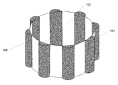
- FIGS. 2A-D illustrate three-dimensional perspective views of a substrate having conductive features at various stages of fabrication.
- FIGS. 3A and 3B illustrate top-level views of example conductive features according to various embodiments.
- FIG. 4 is a process flow diagram of a method to fabricate a semiconductor package described herein.
- Embodiments of the present disclosure describe methods of fabricating through-silicon vias and other similar packaging and integrated circuit features.
- Embodiments include fabricating conductive features that are relatively small, such as vias with diameters less than 20 ⁇ m.
- conventional chemical etching techniques are unsuited for fabricating vias that have relatively small diameters because such techniques result in cone-shaped vias.
- Techniques disclosed herein include drilling relatively large holes in a substrate, coating the interior surfaces of those holes with a conductive material, and then removing a portion of the conductive material so that one or more relatively small vertical conductive features remain within the hole.
- FIGS. 1A-D illustrate top-level views of a substrate having conductive features at various stages of fabrication.
- a hole 102 is formed in substrate 100 .
- the hole 102 is drilled, such as for example using a mechanical drill, laser drill, or some other drill type.
- the hole 102 includes several side features 104 .
- the side features 104 may be grooves, channels, or other features that extend outward from the center of the hole 102 and run lengthwise down the hole 102 from a bottom surface of the substrate 100 to a top surface of the substrate 100 .
- the side features 104 may have different shapes, e.g., round, semi-circular, square or rectangular.
- the substrate 100 may include Silicon (Si), silicon-germanium (SiGe), germanium (Ge), gallium arsenide (GaAs), or other suitable substrate material.
- a conducive material 106 is placed into the hole 102 .
- the conductive material 106 may be, for example, aluminum (Al), copper (Cu), aluminum-copper alloy, nickel (Ni), or other conductive material.
- the conductive material 106 is deposited by electrodeposition, evaporation, a sputtering process, or other suitable process.
- FIG. 1B shows that the hole 102 is completely filled with the conductive material 106 , in embodiments a portion of the hole 102 may be unfilled. An example of this is illustrated in FIG. 1C , where the conductive material 106 is placed into the hole 102 sufficient to coat the internal surface of the hole 102 and to fill the side features 104 .
- One or more lengthwise portions of the conductive material 106 are etched away, such as by employing, for example, chemical etching, or some other etching process.
- the conductive material 106 is shown etched away until one or more conductive features 108 remain.
- the conductive features 108 occupy lengthwise portions of the hole 102 .
- the conductive features 108 are disposed within the side features 104 .
- a material, such as a non-conducting dielectric material may be deposited into a center portion 110 of the hole 102 after the portion of the conductive material 106 has been etched away.
- the dielectric material (not illustrated) may fully or partially fill the center portion 110 .
- the conductive features 108 may be used as through-silicon vias (TSVs), through package vias (TPV), or similar features.
- the conducive material 106 is etched away at least until the resulting conductive features 108 are physically separate from one another.
- the dielectric material deposited into the center portion 110 may enhance the electrical isolation between the conductive features 108 .
- the diameter of the hole 102 may be approximately 50 ⁇ m to 200 ⁇ m, and the widest lateral dimension of the conductive features 108 may be less than 20 ⁇ m, such as on the order of 5 ⁇ m to 20 ⁇ m. Also, adjacent conductive features 108 may be relatively close to one another, such as between 5 ⁇ m and 40 ⁇ m apart. As previously noted, forming a TSV or other conductive feature with such relatively small dimensions using a conventional chemical etching process generally results in cone-shaped TSVs, making it difficult or impossible to space such TSVs close together without one TSV impinging on another TSV.
- conductive features such as conductive features 108
- conductive features 108 that have substantially uniform shape and size along their lengths, and may therefore be spaced relatively close together, thereby occupying less space than if conventional processes for forming conductive features were used.
- FIGS. 1E-I illustrate top-level views of an example embodiment of a conductive feature 108 at various stages of fabrication. While only one conductive feature 108 is illustrated, it is to be understood that FIGS. 1E-I apply to multiple conductive features 108 .
- FIG. 1E illustrates a dielectric or insulating layer 120 being deposited within the hole 102 .
- the dielectric layer 120 is deposited to generally conform to the contours of the side feature 104 .
- the dielectric layer 120 can be etched if desired such as by employing, for example, chemical etching, or some other etching process.
- FIG. 1F illustrates a conductive material being deposited within the hole 102 over the dielectric layer 120 to provide a metal layer 122 .
- the conductive material may be, for example, aluminum (Al), copper (Cu), aluminum-copper alloy, nickel (Ni), or other conductive material.
- the conductive material is deposited by electrodeposition, evaporation, a sputtering process, or other suitable process.
- the metal layer 122 is then etched so that the metal layer 122 is substantially within the conductive feature 108 .
- FIG. 1H illustrates another dielectric layer 124 being deposited within the hole 102 over the metal layer 122 .
- the dielectric layer 124 can be etched if desired. This other dielectric layer 124 is used to insulate the metal layer 122 .
- the center portion 110 of the hole 102 can then be filled with material 126 .
- the material 126 is a dielectric material.
- the dielectric material deposited into the center portion 110 may enhance the electrical isolation between the conductive features 108 .
- the material 126 is a conductive material.
- the conductive material within the hole 102 allows for a connection to, for example, ground.
- FIGS. 2A-D illustrate three-dimensional perspective views of a substrate having conductive features at various stages of fabrication.
- FIG. 2A corresponds to the same or similar stage of fabrication illustrated in FIG. 1A .
- FIG. 2B corresponds to the same or similar stage of fabrication illustrated in FIG. 1B .
- FIG. 2C corresponds to the same or similar stage of fabrication illustrated in FIG. 1C .
- FIG. 2D corresponds to the same or similar stage of fabrication illustrated in FIG. 1D .
- the conductive features 108 traverse a lengthwise dimension of the hole 102 .
- the conductive features 108 can serve as conductors for features situated on or near the top and bottom of the substrate 100 .
- FIGS. 3A and 3B illustrate top-level views of example conductive features according to various embodiments of the present disclosure.
- the examples illustrated in FIGS. 1A-D show the formation of conductive features that wholly occupy the side features, or grooves, formed in the outer edges of the holes.
- the conductive material is etched away such that the conductive features 108 are flush with an interior surface of the hole 102 in which they are formed.
- the example shown in FIG. 3A illustrates a substrate 300 with conductive features 302 formed by etching away the conductive material to a point at which the conductive features are physically separate from one another, but are not flush with the interior surface of the hole and extend inward towards a center of the hole 304 .
- the conductive features 302 formed according to embodiments may take on various shapes.
- triangle-shaped conductive features 310 are formed into a substrate 312 by coating the interior surfaces of a hole 314 having a square-shaped interior portion and triangular-shape side features 316 .
- the example shown in FIG. 3B illustrates conductive features 310 that are flush with the interior of the hole 312
- the conductive features 310 may also be formed such that they extend inward towards the hole, similar to the conductive features 302 illustrated in FIG. 3A .
- FIGS. 1A-D and FIGS. 2A-D include circular holes 102 , with rounded side features 104 .
- embodiments such as, for example, the embodiment illustrated in FIG. 3B , are not limited to circular-shaped holes and rounded side features.
- the inner portion of the holes may be, in various embodiments, substantially square, rectangular, elliptical, triangular, parallelograms, quadrangular, polygonal, and so forth.
- the side features may likewise be, in various embodiments, curved, triangular, square, quadrangular, parallelograms, polygonal, and so forth.
- holes may be formed in the substrate without side features or grooves.
- a square-shaped hole may be formed in a substrate, a conductive material deposited to coat the interior surfaces of the square-shaped hole, and then an etching process utilized to leave only the corners of the square-shaped hole filled with the conductive material, thereby forming four conductive features in the corners that traverse the hole lengthwise.
- Similar embodiments could utilize triangular-shaped holes, star-shaped holes, pentagon-shaped holes, and so forth.
- FIG. 4 is a process flow diagram of an example of a method 400 to fabricate a semiconductor package described herein with respect to FIGS. 1A-D , 2 A-D and 3 A-B.
- a hole is formed in a substrate.
- the substrate may include Silicon (Si), silicon-germanium (SiGe), germanium (Ge), gallium arsenide (GaAs), or other suitable substrate material.
- the hole may be drilled such as with a mechanical or laser drill, or formed in some other suitable manner.
- the hole may include one or more side features, such as grooves or channels, that extend outward from the center of the hole and that traverse a vertical dimension of the hole.
- the hole may be one of various shapes.
- the hole may be substantially square, rectangular, elliptical, triangular, a parallelogram, quadrangular, polygonal, irregular, or some other shape.
- an inner portion of the holes may be, in various embodiments, substantially square, rectangular, elliptical, triangular, a parallelogram, quadrangular, polygonal, irregular, and so forth.
- the side features may be curved, triangular, square, quadrangular, parallelograms, polygonal, irregular, and so forth.
- Embodiments are not limited to holes and side features of any particular shape or shapes.
- a conductive material is deposited into the hole.
- the conductive material may completely or partially fill the hole.
- the conductive material is deposited sufficient to substantially coat the inner surface of the hole, including filling one more side features in embodiments where the hole is formed with one or more side features.
- the conductive material may be aluminum (Al), aluminum-copper alloy, copper (Cu), nickel (Ni), or other conductive material.
- a part of the conductive material is removed from the hole.
- a part of the conductive material that occupies a first lengthwise portion of the hole is removed, such that at least one contiguous portion of the conductive material that occupies a second lengthwise portion of the hole remains in the substrate.
- the part of the substrate that is removed previously traversed the length of the hole, and the part of the substrate that remains also traverses the length of the hole.
- the portion of the conductive material that remains is at least partially disposed in one of the side features. Where multiple side features are present in the hole, multiple parts of the conductive material remain in the hole, at least partly situated in the side features.
- the multiple conductive features are physically separate from one another, such that they are usable as separate vias or other conductive feature types. Multiple conductive features may be created concurrently according to various embodiments.
- a dielectric material is deposited into the hole.
- the dielectric material may occupy all or some of the space where the conductive material was removed from the hole, and may serve to physically and/or electrically isolate the conductive features from one another.
- the phrase “A/B” means A or B.
- the phrase “A and/or B” means “(A), (B), or (A and B).”
- the phrase “at least one of A, B, and C” means “(A), (B), (C), (A and B), (A and C), (B and C), or (A, B and C).”
- the phrase “(A)B” means “(B) or (AB)” that is, A is an optional element.
Abstract
Description
Claims (23)
Priority Applications (1)
| Application Number | Priority Date | Filing Date | Title |
|---|---|---|---|
| US14/500,692 US9312176B2 (en) | 2011-10-03 | 2014-09-29 | Removing conductive material to form conductive features in a substrate |
Applications Claiming Priority (3)
| Application Number | Priority Date | Filing Date | Title |
|---|---|---|---|
| US201161542744P | 2011-10-03 | 2011-10-03 | |
| US13/633,825 US8847364B2 (en) | 2011-10-03 | 2012-10-02 | Removing conductive material to form conductive features in a substrate |
| US14/500,692 US9312176B2 (en) | 2011-10-03 | 2014-09-29 | Removing conductive material to form conductive features in a substrate |
Related Parent Applications (1)
| Application Number | Title | Priority Date | Filing Date |
|---|---|---|---|
| US13/633,825 Continuation US8847364B2 (en) | 2011-10-03 | 2012-10-02 | Removing conductive material to form conductive features in a substrate |
Publications (2)
| Publication Number | Publication Date |
|---|---|
| US20150024590A1 US20150024590A1 (en) | 2015-01-22 |
| US9312176B2 true US9312176B2 (en) | 2016-04-12 |
Family
ID=47991785
Family Applications (2)
| Application Number | Title | Priority Date | Filing Date |
|---|---|---|---|
| US13/633,825 Expired - Fee Related US8847364B2 (en) | 2011-10-03 | 2012-10-02 | Removing conductive material to form conductive features in a substrate |
| US14/500,692 Expired - Fee Related US9312176B2 (en) | 2011-10-03 | 2014-09-29 | Removing conductive material to form conductive features in a substrate |
Family Applications Before (1)
| Application Number | Title | Priority Date | Filing Date |
|---|---|---|---|
| US13/633,825 Expired - Fee Related US8847364B2 (en) | 2011-10-03 | 2012-10-02 | Removing conductive material to form conductive features in a substrate |
Country Status (5)
| Country | Link |
|---|---|
| US (2) | US8847364B2 (en) |
| EP (1) | EP2764537A1 (en) |
| CN (1) | CN103946972B (en) |
| TW (1) | TWI545711B (en) |
| WO (1) | WO2013050877A1 (en) |
Citations (9)
| Publication number | Priority date | Publication date | Assignee | Title |
|---|---|---|---|---|
| US4543715A (en) | 1983-02-28 | 1985-10-01 | Allied Corporation | Method of forming vertical traces on printed circuit board |
| US6077780A (en) * | 1997-12-03 | 2000-06-20 | Advanced Micro Devices, Inc. | Method for filling high aspect ratio openings of an integrated circuit to minimize electromigration failure |
| US20040251047A1 (en) | 2003-06-12 | 2004-12-16 | International Business Machines Corporation | Via structure for increased wiring on printed wiring boards |
| US20060043598A1 (en) | 2004-08-31 | 2006-03-02 | Kirby Kyle K | Methods of manufacture of a via structure comprising a plurality of conductive elements, semiconductor die, multichip module, and system including same |
| US20060148250A1 (en) | 2004-12-30 | 2006-07-06 | Micron Technology, Inc. | Methods for forming interconnects in microelectronic workpieces and microelectronic workpieces formed using such methods |
| US20090057912A1 (en) * | 2007-08-31 | 2009-03-05 | Micron Technology, Inc. | Partitioned through-layer via and associated systems and methods |
| US20090243120A1 (en) | 2008-03-25 | 2009-10-01 | Panasonic Corporation | Semiconductor element and semiconductor element fabrication method |
| US20100314742A1 (en) | 2009-06-15 | 2010-12-16 | Sung Min Kim | Semiconductor package |
| US7994044B2 (en) * | 2009-09-03 | 2011-08-09 | Ati Technologies Ulc | Semiconductor chip with contoured solder structure opening |
Family Cites Families (1)
| Publication number | Priority date | Publication date | Assignee | Title |
|---|---|---|---|---|
| US8405196B2 (en) * | 2007-03-05 | 2013-03-26 | DigitalOptics Corporation Europe Limited | Chips having rear contacts connected by through vias to front contacts |
-
2012
- 2012-10-02 US US13/633,825 patent/US8847364B2/en not_active Expired - Fee Related
- 2012-10-03 EP EP12816499.3A patent/EP2764537A1/en not_active Withdrawn
- 2012-10-03 TW TW101136601A patent/TWI545711B/en not_active IP Right Cessation
- 2012-10-03 WO PCT/IB2012/002580 patent/WO2013050877A1/en active Application Filing
- 2012-10-03 CN CN201280057102.6A patent/CN103946972B/en not_active Expired - Fee Related
-
2014
- 2014-09-29 US US14/500,692 patent/US9312176B2/en not_active Expired - Fee Related
Patent Citations (10)
| Publication number | Priority date | Publication date | Assignee | Title |
|---|---|---|---|---|
| US4543715A (en) | 1983-02-28 | 1985-10-01 | Allied Corporation | Method of forming vertical traces on printed circuit board |
| US6077780A (en) * | 1997-12-03 | 2000-06-20 | Advanced Micro Devices, Inc. | Method for filling high aspect ratio openings of an integrated circuit to minimize electromigration failure |
| US20040251047A1 (en) | 2003-06-12 | 2004-12-16 | International Business Machines Corporation | Via structure for increased wiring on printed wiring boards |
| US20060043598A1 (en) | 2004-08-31 | 2006-03-02 | Kirby Kyle K | Methods of manufacture of a via structure comprising a plurality of conductive elements, semiconductor die, multichip module, and system including same |
| US20060148250A1 (en) | 2004-12-30 | 2006-07-06 | Micron Technology, Inc. | Methods for forming interconnects in microelectronic workpieces and microelectronic workpieces formed using such methods |
| US20090008780A1 (en) | 2004-12-30 | 2009-01-08 | Micron Technology, Inc. | Methods for forming interconnects in microelectronic workpieces and microelectronic workpieces formed using such methods |
| US20090057912A1 (en) * | 2007-08-31 | 2009-03-05 | Micron Technology, Inc. | Partitioned through-layer via and associated systems and methods |
| US20090243120A1 (en) | 2008-03-25 | 2009-10-01 | Panasonic Corporation | Semiconductor element and semiconductor element fabrication method |
| US20100314742A1 (en) | 2009-06-15 | 2010-12-16 | Sung Min Kim | Semiconductor package |
| US7994044B2 (en) * | 2009-09-03 | 2011-08-09 | Ati Technologies Ulc | Semiconductor chip with contoured solder structure opening |
Also Published As
| Publication number | Publication date |
|---|---|
| TWI545711B (en) | 2016-08-11 |
| US8847364B2 (en) | 2014-09-30 |
| US20130082359A1 (en) | 2013-04-04 |
| CN103946972B (en) | 2017-08-04 |
| US20150024590A1 (en) | 2015-01-22 |
| WO2013050877A1 (en) | 2013-04-11 |
| EP2764537A1 (en) | 2014-08-13 |
| TW201322403A (en) | 2013-06-01 |
| CN103946972A (en) | 2014-07-23 |
Similar Documents
| Publication | Publication Date | Title |
|---|---|---|
| US20200258865A1 (en) | Stacked Integrated Circuits with Redistribution Lines | |
| US7750441B2 (en) | Conductive interconnects along the edge of a microelectronic device | |
| DE112010005236B4 (en) | Backside pseudo plug for 3D integration | |
| CN102446865B (en) | Crack stop barrier and manufacture method thereof | |
| US20110193197A1 (en) | Structure and method for making crack stop for 3d integrated circuits | |
| TWI515859B (en) | Interconnection structure and fabrication thereof | |
| KR101556474B1 (en) | Monitor structures | |
| US9991204B2 (en) | Through via structure for step coverage improvement | |
| US11145623B2 (en) | Integrated circuit packages and methods of forming the same | |
| EP3306654B1 (en) | Method for etching through-silicon vias and corresponding semiconductor device | |
| US9165895B2 (en) | Method for separating a plurality of dies and a processing device for separating a plurality of dies | |
| US9312176B2 (en) | Removing conductive material to form conductive features in a substrate | |
| WO2024021631A1 (en) | Through-silicon-via structure and manufacturing method therefor | |
| US20220254739A1 (en) | Specificatdevices with through silicon vias, guard rings and methods of making the same | |
| WO2022241962A1 (en) | Chip, memory, and preparation method for chip | |
| DE102020124580A1 (en) | WAFER BONDING METHOD | |
| US8951833B2 (en) | Defect free deep trench method for semiconductor chip | |
| US20130277798A1 (en) | Implementing Semiconductor Signal-Capable Capacitors with Deep Trench and TSV Technologies | |
| CN109300877B (en) | Through hole structure in semiconductor substrate and manufacturing method thereof | |
| TWI482548B (en) | Manufacturing method of circuit structure | |
| CN113539945A (en) | Semiconductor structure and forming method thereof | |
| TW201533874A (en) | Chip structure having pillar bump embedded in TSV | |
| TW201448116A (en) | Forming fence conductors in an integrated circuit |
Legal Events
| Date | Code | Title | Description |
|---|---|---|---|
| STCF | Information on status: patent grant |
Free format text: PATENTED CASE |
|
| FEPP | Fee payment procedure |
Free format text: MAINTENANCE FEE REMINDER MAILED (ORIGINAL EVENT CODE: REM.); ENTITY STATUS OF PATENT OWNER: LARGE ENTITY |
|
| AS | Assignment |
Owner name: MARVELL INTERNATIONAL LTD., BERMUDA Free format text: ASSIGNMENT OF ASSIGNORS INTEREST;ASSIGNOR:MARVELL WORLD TRADE LTD.;REEL/FRAME:051778/0537 Effective date: 20191231 |
|
| AS | Assignment |
Owner name: CAVIUM INTERNATIONAL, CAYMAN ISLANDS Free format text: ASSIGNMENT OF ASSIGNORS INTEREST;ASSIGNOR:MARVELL INTERNATIONAL LTD.;REEL/FRAME:052918/0001 Effective date: 20191231 |
|
| LAPS | Lapse for failure to pay maintenance fees |
Free format text: PATENT EXPIRED FOR FAILURE TO PAY MAINTENANCE FEES (ORIGINAL EVENT CODE: EXP.); ENTITY STATUS OF PATENT OWNER: LARGE ENTITY |
|
| STCH | Information on status: patent discontinuation |
Free format text: PATENT EXPIRED DUE TO NONPAYMENT OF MAINTENANCE FEES UNDER 37 CFR 1.362 |
|
| FP | Lapsed due to failure to pay maintenance fee |
Effective date: 20200412 |
|
| AS | Assignment |
Owner name: MARVELL ASIA PTE, LTD., SINGAPORE Free format text: ASSIGNMENT OF ASSIGNORS INTEREST;ASSIGNOR:CAVIUM INTERNATIONAL;REEL/FRAME:053475/0001 Effective date: 20191231 |