US9298636B1 - Managing data storage - Google Patents
Managing data storage Download PDFInfo
- Publication number
- US9298636B1 US9298636B1 US13/248,219 US201113248219A US9298636B1 US 9298636 B1 US9298636 B1 US 9298636B1 US 201113248219 A US201113248219 A US 201113248219A US 9298636 B1 US9298636 B1 US 9298636B1
- Authority
- US
- United States
- Prior art keywords
- data storage
- write
- data
- response
- processor
- Prior art date
- Legal status (The legal status is an assumption and is not a legal conclusion. Google has not performed a legal analysis and makes no representation as to the accuracy of the status listed.)
- Active, expires
Links
Images


Classifications
-
- G—PHYSICS
- G06—COMPUTING; CALCULATING OR COUNTING
- G06F—ELECTRIC DIGITAL DATA PROCESSING
- G06F12/00—Accessing, addressing or allocating within memory systems or architectures
- G06F12/02—Addressing or allocation; Relocation
- G06F12/08—Addressing or allocation; Relocation in hierarchically structured memory systems, e.g. virtual memory systems
- G06F12/0802—Addressing of a memory level in which the access to the desired data or data block requires associative addressing means, e.g. caches
- G06F12/0888—Addressing of a memory level in which the access to the desired data or data block requires associative addressing means, e.g. caches using selective caching, e.g. bypass
-
- G—PHYSICS
- G06—COMPUTING; CALCULATING OR COUNTING
- G06F—ELECTRIC DIGITAL DATA PROCESSING
- G06F12/00—Accessing, addressing or allocating within memory systems or architectures
- G06F12/02—Addressing or allocation; Relocation
- G06F12/08—Addressing or allocation; Relocation in hierarchically structured memory systems, e.g. virtual memory systems
- G06F12/0802—Addressing of a memory level in which the access to the desired data or data block requires associative addressing means, e.g. caches
- G06F12/0893—Caches characterised by their organisation or structure
- G06F12/0895—Caches characterised by their organisation or structure of parts of caches, e.g. directory or tag array
-
- G—PHYSICS
- G06—COMPUTING; CALCULATING OR COUNTING
- G06F—ELECTRIC DIGITAL DATA PROCESSING
- G06F11/00—Error detection; Error correction; Monitoring
-
- G—PHYSICS
- G06—COMPUTING; CALCULATING OR COUNTING
- G06F—ELECTRIC DIGITAL DATA PROCESSING
- G06F11/00—Error detection; Error correction; Monitoring
- G06F11/07—Responding to the occurrence of a fault, e.g. fault tolerance
- G06F11/14—Error detection or correction of the data by redundancy in operation
-
- G—PHYSICS
- G06—COMPUTING; CALCULATING OR COUNTING
- G06F—ELECTRIC DIGITAL DATA PROCESSING
- G06F11/00—Error detection; Error correction; Monitoring
- G06F11/07—Responding to the occurrence of a fault, e.g. fault tolerance
- G06F11/16—Error detection or correction of the data by redundancy in hardware
- G06F11/20—Error detection or correction of the data by redundancy in hardware using active fault-masking, e.g. by switching out faulty elements or by switching in spare elements
- G06F11/2053—Error detection or correction of the data by redundancy in hardware using active fault-masking, e.g. by switching out faulty elements or by switching in spare elements where persistent mass storage functionality or persistent mass storage control functionality is redundant
- G06F11/2056—Error detection or correction of the data by redundancy in hardware using active fault-masking, e.g. by switching out faulty elements or by switching in spare elements where persistent mass storage functionality or persistent mass storage control functionality is redundant by mirroring
- G06F11/2058—Error detection or correction of the data by redundancy in hardware using active fault-masking, e.g. by switching out faulty elements or by switching in spare elements where persistent mass storage functionality or persistent mass storage control functionality is redundant by mirroring using more than 2 mirrored copies
-
- G—PHYSICS
- G06—COMPUTING; CALCULATING OR COUNTING
- G06F—ELECTRIC DIGITAL DATA PROCESSING
- G06F11/00—Error detection; Error correction; Monitoring
- G06F11/07—Responding to the occurrence of a fault, e.g. fault tolerance
- G06F11/16—Error detection or correction of the data by redundancy in hardware
- G06F11/20—Error detection or correction of the data by redundancy in hardware using active fault-masking, e.g. by switching out faulty elements or by switching in spare elements
- G06F11/2053—Error detection or correction of the data by redundancy in hardware using active fault-masking, e.g. by switching out faulty elements or by switching in spare elements where persistent mass storage functionality or persistent mass storage control functionality is redundant
- G06F11/2056—Error detection or correction of the data by redundancy in hardware using active fault-masking, e.g. by switching out faulty elements or by switching in spare elements where persistent mass storage functionality or persistent mass storage control functionality is redundant by mirroring
- G06F11/2064—Error detection or correction of the data by redundancy in hardware using active fault-masking, e.g. by switching out faulty elements or by switching in spare elements where persistent mass storage functionality or persistent mass storage control functionality is redundant by mirroring while ensuring consistency
-
- G—PHYSICS
- G06—COMPUTING; CALCULATING OR COUNTING
- G06F—ELECTRIC DIGITAL DATA PROCESSING
- G06F11/00—Error detection; Error correction; Monitoring
- G06F11/07—Responding to the occurrence of a fault, e.g. fault tolerance
- G06F11/16—Error detection or correction of the data by redundancy in hardware
- G06F11/20—Error detection or correction of the data by redundancy in hardware using active fault-masking, e.g. by switching out faulty elements or by switching in spare elements
- G06F11/2053—Error detection or correction of the data by redundancy in hardware using active fault-masking, e.g. by switching out faulty elements or by switching in spare elements where persistent mass storage functionality or persistent mass storage control functionality is redundant
- G06F11/2056—Error detection or correction of the data by redundancy in hardware using active fault-masking, e.g. by switching out faulty elements or by switching in spare elements where persistent mass storage functionality or persistent mass storage control functionality is redundant by mirroring
- G06F11/2071—Error detection or correction of the data by redundancy in hardware using active fault-masking, e.g. by switching out faulty elements or by switching in spare elements where persistent mass storage functionality or persistent mass storage control functionality is redundant by mirroring using a plurality of controllers
- G06F11/2076—Synchronous techniques
-
- G—PHYSICS
- G06—COMPUTING; CALCULATING OR COUNTING
- G06F—ELECTRIC DIGITAL DATA PROCESSING
- G06F11/00—Error detection; Error correction; Monitoring
- G06F11/07—Responding to the occurrence of a fault, e.g. fault tolerance
- G06F11/16—Error detection or correction of the data by redundancy in hardware
- G06F11/20—Error detection or correction of the data by redundancy in hardware using active fault-masking, e.g. by switching out faulty elements or by switching in spare elements
- G06F11/2053—Error detection or correction of the data by redundancy in hardware using active fault-masking, e.g. by switching out faulty elements or by switching in spare elements where persistent mass storage functionality or persistent mass storage control functionality is redundant
- G06F11/2089—Redundant storage control functionality
-
- G—PHYSICS
- G06—COMPUTING; CALCULATING OR COUNTING
- G06F—ELECTRIC DIGITAL DATA PROCESSING
- G06F11/00—Error detection; Error correction; Monitoring
- G06F11/30—Monitoring
- G06F11/3003—Monitoring arrangements specially adapted to the computing system or computing system component being monitored
- G06F11/3024—Monitoring arrangements specially adapted to the computing system or computing system component being monitored where the computing system component is a central processing unit [CPU]
-
- G—PHYSICS
- G06—COMPUTING; CALCULATING OR COUNTING
- G06F—ELECTRIC DIGITAL DATA PROCESSING
- G06F11/00—Error detection; Error correction; Monitoring
- G06F11/30—Monitoring
- G06F11/3003—Monitoring arrangements specially adapted to the computing system or computing system component being monitored
- G06F11/3034—Monitoring arrangements specially adapted to the computing system or computing system component being monitored where the computing system component is a storage system, e.g. DASD based or network based
-
- G—PHYSICS
- G06—COMPUTING; CALCULATING OR COUNTING
- G06F—ELECTRIC DIGITAL DATA PROCESSING
- G06F11/00—Error detection; Error correction; Monitoring
- G06F11/30—Monitoring
- G06F11/3003—Monitoring arrangements specially adapted to the computing system or computing system component being monitored
- G06F11/3041—Monitoring arrangements specially adapted to the computing system or computing system component being monitored where the computing system component is an input/output interface
-
- G—PHYSICS
- G06—COMPUTING; CALCULATING OR COUNTING
- G06F—ELECTRIC DIGITAL DATA PROCESSING
- G06F3/00—Input arrangements for transferring data to be processed into a form capable of being handled by the computer; Output arrangements for transferring data from processing unit to output unit, e.g. interface arrangements
- G06F3/06—Digital input from, or digital output to, record carriers, e.g. RAID, emulated record carriers or networked record carriers
- G06F3/0601—Interfaces specially adapted for storage systems
- G06F3/0602—Interfaces specially adapted for storage systems specifically adapted to achieve a particular effect
- G06F3/061—Improving I/O performance
-
- G—PHYSICS
- G06—COMPUTING; CALCULATING OR COUNTING
- G06F—ELECTRIC DIGITAL DATA PROCESSING
- G06F3/00—Input arrangements for transferring data to be processed into a form capable of being handled by the computer; Output arrangements for transferring data from processing unit to output unit, e.g. interface arrangements
- G06F3/06—Digital input from, or digital output to, record carriers, e.g. RAID, emulated record carriers or networked record carriers
- G06F3/0601—Interfaces specially adapted for storage systems
- G06F3/0628—Interfaces specially adapted for storage systems making use of a particular technique
- G06F3/0629—Configuration or reconfiguration of storage systems
- G06F3/0635—Configuration or reconfiguration of storage systems by changing the path, e.g. traffic rerouting, path reconfiguration
-
- G—PHYSICS
- G06—COMPUTING; CALCULATING OR COUNTING
- G06F—ELECTRIC DIGITAL DATA PROCESSING
- G06F3/00—Input arrangements for transferring data to be processed into a form capable of being handled by the computer; Output arrangements for transferring data from processing unit to output unit, e.g. interface arrangements
- G06F3/06—Digital input from, or digital output to, record carriers, e.g. RAID, emulated record carriers or networked record carriers
- G06F3/0601—Interfaces specially adapted for storage systems
- G06F3/0628—Interfaces specially adapted for storage systems making use of a particular technique
- G06F3/0655—Vertical data movement, i.e. input-output transfer; data movement between one or more hosts and one or more storage devices
- G06F3/0659—Command handling arrangements, e.g. command buffers, queues, command scheduling
-
- G—PHYSICS
- G06—COMPUTING; CALCULATING OR COUNTING
- G06F—ELECTRIC DIGITAL DATA PROCESSING
- G06F3/00—Input arrangements for transferring data to be processed into a form capable of being handled by the computer; Output arrangements for transferring data from processing unit to output unit, e.g. interface arrangements
- G06F3/06—Digital input from, or digital output to, record carriers, e.g. RAID, emulated record carriers or networked record carriers
- G06F3/0601—Interfaces specially adapted for storage systems
- G06F3/0668—Interfaces specially adapted for storage systems adopting a particular infrastructure
- G06F3/0671—In-line storage system
- G06F3/0683—Plurality of storage devices
-
- G—PHYSICS
- G06—COMPUTING; CALCULATING OR COUNTING
- G06F—ELECTRIC DIGITAL DATA PROCESSING
- G06F11/00—Error detection; Error correction; Monitoring
- G06F11/07—Responding to the occurrence of a fault, e.g. fault tolerance
- G06F11/16—Error detection or correction of the data by redundancy in hardware
- G06F11/20—Error detection or correction of the data by redundancy in hardware using active fault-masking, e.g. by switching out faulty elements or by switching in spare elements
- G06F11/2015—Redundant power supplies
-
- G—PHYSICS
- G06—COMPUTING; CALCULATING OR COUNTING
- G06F—ELECTRIC DIGITAL DATA PROCESSING
- G06F2212/00—Indexing scheme relating to accessing, addressing or allocation within memory systems or architectures
- G06F2212/10—Providing a specific technical effect
- G06F2212/1016—Performance improvement
- G06F2212/1024—Latency reduction
Definitions
- the present invention relates to managing data storage.
- Computer systems may include different resources used by one or more hosts. Resources and hosts in a computer system may be interconnected by one or more communication connections. These resources may include, for example, data storage devices such as those included in the data storage systems manufactured by EMC Corporation. These data storage systems may be coupled to one or more servers or hosts and provide storage services to each host. Multiple data storage systems from one or more different vendors may be connected and may provide common data storage for one or more hosts in a computer system.
- the hosts may access data by sending access requests to the one or more storage systems.
- Some storage systems require that the access requests identify units of data to be accessed using logical volume and block addresses that define where the units of data are stored on the storage system.
- Such storage systems are known as “block I/O” storage systems.
- the logical volumes presented by the storage system to the host correspond directly to physical storage devices (e.g., disk drives) on the storage system, so that the specification of a logical volume and block address specifies where the data is physically stored within the storage system.
- internal mapping techniques may be employed so that the logical volumes presented by the storage system do not necessarily map in a one-to-one manner to physical storage devices within the storage system. Nevertheless, the specification of a logical volume and a block address used with an intelligent storage system specifies where associated content is logically stored within the storage system, and from the perspective of the host is perceived as specifying where the data is physically stored.
- some storage systems receive and process access requests that identify a data unit or other content unit (also referenced to as an object) using an object identifier, rather than an address that specifies where the data unit is physically or logically stored in the storage system.
- object addressable storage OAS
- a content unit may be identified using its object identifier and the object identifier may be independent of both the physical and logical location(s) at which the content unit is stored (although it is not required to be because in some embodiments the storage system may use the object identifier to inform where a content unit is stored in a storage system).
- the object identifier does not control where the content unit is logically (or physically) stored.
- the identifier by which host computer(s) access the unit of content may remain the same.
- data storage systems may utilize a variety of different techniques in connection with write or update operations.
- block I/O storage systems or OAS systems or other storage systems such as a file system storage architecture
- write back caching the data storage system may temporarily cache data received from a host within its storage cache and destage the cached data at different times onto the physical disk drives.
- the cache may be implemented using fast storage media such as RAM (random access memory), dynamic RAM (DRAM), FLASH memory or FLASH drives.
- the data storage system may utilize a backup or secondary power supply for use in connection with preventing loss of cached data in the event of a power failure.
- the data storage system may utilize the backup power supply to provide power to the storage processor and physical data storage devices of the data storage system for a short period of time.
- the storage processor stores the data from its cache to a dedicated area on the storage devices that may be referred to as a “vault” so that the vault includes the cached data which has not yet been destaged onto the physical storage devices.
- a data storage system may include multiple storage processors storing data to a same set of storage devices.
- Each of the storage processors may have its own cache so that cached data for the above operations, as well as possibly other cached data, may be mirrored in the caches of the storage processors.
- Multiple storage processors may be desirable for use in providing fault tolerance and the like.
- a method and a system for use in managing data storage is disclosed.
- Data storage is managed in a data storage system comprising a first and a second storage processor and a plurality of data storage devices.
- the first and the second storage processor having respective caches configured to mirror each other.
- a write I/O is received in the data storage system, wherein the write I/O is an operation for updating data storage in the data storage system.
- Load associated with the first and second storage processor in the data storage system is determined.
- the cache is bypassed and write I/O is delivered to the plurality of data storage devices in the data storage system in response to determining a heavy load associated with the first and second storage processor in the data storage system.
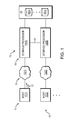
- FIG. 1 is a block diagram of a system that may utilize the techniques described herein;
- FIG. 2 is a block diagram of components of a system that may utilize the techniques described herein;
- FIG. 3 is a flowchart summarizing the steps for managing data storage.
- the invention can be implemented in numerous ways, including as a process, an apparatus, a system, a computer program embodied on a computer readable storage medium, and/or a processor, such as a processor configured to execute instructions stored on and/or provided by a memory coupled to the processor.
- a processor such as a processor configured to execute instructions stored on and/or provided by a memory coupled to the processor.
- the implementations, or any other form that the invention may take, may be referred to as techniques.
- the order of the steps of disclosed processes may be altered within the scope of the invention.
- a component such as a processor or a memory described as being configured to perform a task may be implemented as a general component that is temporarily configured to perform the task at a given time or a specific component that is manufactured to perform the task.
- the term ‘processor’ refers to one or more devices, circuits, and/or processing cores configured to process data, such as computer program instructions.
- the technique is suitable for managing, but not limited to, high bandwidth write requests that optimizes the use of storage processor compute and memory system resources to improve the throughput achievable on the storage processor. It does so by dynamically deciding which I/Os to mirror and which not to mirror between the storage processors. By selectively mirroring writes, it improves the system throughput under heavy load.
- the prior art techniques nearly always mirrored write data between controllers and performed a later lazy flush using substantial CPU and memory system resources.
- the techniques never mirrored write data between controllers and limited the size of I/Os that can be performed on the backend.
- the dynamic bandwidth optimization can deliver advantages over these approaches. For example, it can reduce CPU and memory system resources by not mirroring all the data.
- the system 10 comprises host computers 11 ( 1 ), 11 ( 2 ), . . . (collectively, hosts 11 ) connectable to a data storage system 12 via communications medium 13 ( 1 ), 13 ( 2 ), . . . (collectively, communications media 13 ).
- the data storage system 12 comprises multiple storage processors 14 (A), 14 (B) (collectively, storage processors 14 ), a cache mirror bus 15 and a set of data storage devices, for example, disk drives 16 ( 1 ), . . . 16 (N) (collectively, disk drives 16 ).
- the host 11 ( 1 ) is shown communicating with storage processor 14 (A) and the host 11 ( 2 ) is shown communicating with storage processor 14 (B). However, it will be readily apparent to those skilled in the art that this is for illustration purposes and that the host 11 ( 1 ) may have connections with and communicate with any storage processor 14 . It will also be apparent that similar comments also apply to the other host 11 ( 2 ).
- the storage processors 14 may be configured to perform data storage operations (e.g., read operations, write operations, etc.) on behalf of the hosts 11 .
- the cache mirror bus 15 may be configured to convey data between caches of the storage processors 14 thus enabling cache mirroring between the storage processors 14 .
- the set of disk drives 16 enables the data storage system 12 to store and retrieve data on behalf of the hosts 11 in a fault tolerant, non-volatile manner (e.g., using a RAID scheme).
- Each storage processor 14 may be configured to perform write-back caching in response to write operations 17 from the hosts 11 while both storage processors 14 are in operation. That is the storage processor 14 acknowledges completion of a write operation 17 to the host after the data has been stored in its cache as well as mirrored to the cache of the other storage processor. Such operations enable the data storage system 12 to provide improved response times.
- cache mirroring as described above may be performed over any communication channel between storage processors which may include frontend interfaces, backend interfaces, or some dedicated storage processor to storage processor interfaces. Additionally, it will be appreciated that there may be more than one interface on a storage processor that can be used for cache mirroring and the implementation may distribute mirroring requests across the multiple interfaces based on some load balancing policy. Moreover, it will be appreciated that cache mirroring may be performed over hardwired interfaces like dedicated cables or signals carried over a mid-plane between controllers. Alternatively cache mirror may be performed over networks such as Ethernet, fibre channel, SAS, or PCI networks. Furthermore, it will be appreciated that cache mirroring may be performed between collections of more than two storage processors, with cache data being hosted in two or more storage processors to protect against storage processor failure.
- the storage processor 14 may include a communications interface 21 , a controller 22 and a memory subsystem 23 .
- the communications interface 21 may include a host interface 24 , a cache mirroring interface 25 , and a disk interface 26 .
- the memory subsystem 23 may include a control circuit 27 , cache 28 and additional memory 29 .
- the additional memory 29 includes operating system storage, firmware for storing BIOS and POST code, optional flash memory, etc.
- the cache 28 may have separate read and write cache memory in the storage processor.
- the cache 28 may be a unified read/write cache with pages of the cache holding cache read data, dirty cached write data, or clean cached write data.
- the dirty cached write data may be data written by the host that has not yet been written to disk.
- the clean cached write data may be data written by the host that has been written to disk but is still in the cache. It will also be appreciated that in certain instances the cached read data may not be mirrored between storage processors but cached write data may be mirrored.
- the communications interface 21 may be configured to provide connectivity from the storage processor 14 to various other components.
- the host interface 24 may be configured to connect the storage processor 14 to one or more hosts 11 through the communications media 13 .
- the cache mirroring interface 25 may be configured to connect the storage processor 14 (e.g., the storage processor 14 (A)) to another storage processor 14 (e.g., the storage processor 14 (B)) to enable cache mirroring through the cache mirror bus 15 .
- the disk interface 26 may be configured to connect the storage processor 14 to the set of disk drives 16 .
- the controller 22 may be configured to carryout data storage operations on behalf of one or more of the hosts 11 through the communications interface 21 (e.g., the write operations 17 in FIG. 1 ).
- the controller 22 may be implemented as a set of processors running an operating system which is capable of being stored in a designated area on one or more of the disk drives 16 .
- the controller 22 may be implemented as logic circuitry (e.g., Application Specific Integrated Circuitry, Field Programmable Gate Arrays, etc.), microprocessors or processor chip sets, analog circuitry, various combinations thereof, and so on.
- the memory subsystem 23 may be configured to provide memory services to the controller 22 .
- the control circuitry 27 of the memory subsystem 23 may be configured to provide logic for use with the cache 28 so as to manage the data storage as described herein. It will be appreciated that the control circuit 27 may be further capable of performing other tasks using the additional memory 29 such as vaulting contents of the cache 28 into non-volatile flash memory or disk drive memory in response to a failure of the controller 22 and the like.
- the technique can manage data storage 31 in a data storage system comprising a first and a second storage processor and a plurality of data storage devices wherein the first and second storage processors have respective caches configured to mirror each other.
- the data storage devices may be disk drives.
- a write I/O or write operation is any operation that updates data storage in the data storage system.
- the write I/O may be the data to be forwarded to the data storage devices in the data storage system.
- the write I/O may initially be a command or request from a host for permission to forward data associated with the write I/O to the data storage system. The data may subsequently be forwarded in response to a reply from the data storage system that it is in order to send the data in connection with the write I/O.
- SCSI commands such as WRITE SAME, EXTENDED COPY and the like may be considered for the purposes of this disclosure as write I/O.
- file or object systems may have other commands including update commands like TRUNCATE or DELETE that may also for the purposes of this disclosure be considered as write I/O. It will be appreciated that any other update command may also be considered as a write I/O.
- the technique can determine 33 load associated with the first and second storage processor in the data storage system. For example, the state of the load may be determined 34 to be a heavy load or a light load. Moreover, the technique can bypass cache and deliver 35 the write I/O to the plurality of data storage devices in the data storage system in response to determining a heavy load associated with the first and second storage processor in the data storage system. Alternatively, the technique can deliver 36 the write I/O to cache so that the write I/O can be mirrored in the respective cache in response to determining a light load associated with the first and second storage processor in the data storage system.
- the technique can determine the load by monitoring the activity on a communications link that facilitates mirroring between the respective cache in the first and second storage processor.
- the communications link may be the cache mirror bus 15 of FIG. 1 .
- the technique can determine a heavy load associated with the first and second storage processor in response to monitoring a high amount of activity on the communications link between the cache in the first and second storage processor. Based on determining a heavy load, the technique can bypass cache and deliver the write I/O to the data storage devices.
- the technique can determine a light load associated with the first and second storage processor in response to monitoring a low amount of activity on the communications link between the cache in the first and second storage processor. Based on determining a light load, the technique can deliver the write I/O to cache.
- the advantage of monitoring the communications link for activity is that if a bottleneck occurs in the storage processors the technique is immediately aware and may decide to avoid mirroring thereby increasing the overall performance of the system by bypassing cache and delivering write I/O direct to the data storage devices.
- the technique can determine the load by monitoring the CPU utilization in connection with the first and second storage processor.
- the technique can determine a heavy load associated with the first and second storage processor in response to monitoring a high CPU utilization in connection with the first and second storage processor. Based on determining a heavy load, the technique can bypass cache and deliver the write I/O to the data storage devices.
- the technique can determine a light load associated with the first and second storage processor in response to monitoring a low CPU utilization in connection with the first and second storage processor. Based on determining a light load, the technique can deliver the write I/O to cache.
- the technique can determine the load by monitoring the memory bandwidth utilization in connection with the first and second storage processor.
- the technique can determine a heavy load associated with the first and second storage processor in response to monitoring high memory bandwidth utilization in connection with the first and second storage processor. Based on determining a heavy load, the technique can bypass cache and deliver the write I/O to the data storage devices.
- the technique can determine a light load associated with the first and second storage processor in response to monitoring low memory bandwidth utilization in connection with the first and second storage processor. Based on determining a light load, the technique can deliver the write I/O to cache.
- the technique can determine first and second response times in response to determining the load associated with the respective first and second storage processor.
- the first and second response times may be the response times for a write-back in the event of delivering the write I/O to mirrored cache and the storage devices, respectively.
- the decision to deliver the write I/O to the mirrored cache or storage devices may be dependent on the lowest response time. For example, if the load associated with cache in the respective first and second storage processor in the data storage system is a light load, the response time in connection with caching the write I/O may be determined to be lower than the response time of bypassing cache and delivering the write I/O directly to the data storage devices in the backend of the data storage system. Alternatively, if the storage processors present a bottleneck to the write I/O, it may be more efficient to deliver the write I/O directly to the data storage device bypassing the respective caches as the response time may be determined to be substantially similar or even lower.
- cache mirroring can take up substantial resources in the data storage system. For example, the CPU and memory overhead in connection with cache mirroring can be considerable.
- the advantage of the above technique is that it can manage high bandwidth write requests by optimizing the use of storage processor compute and memory system resources while at the same time improving the throughput achievable on the storage processor.
- the technique as described does so by dynamically deciding which write I/O to mirror.
- the technique can improve the overall performance of the system by selectively delivering the write I/O to either cache or direct to data storage devices in response to determining the load associated with the first and second storage processor in the data storage system.
- mirrored cache may not be as good depending on the state of the load associated with the first and second storage processor in the data storage system. For example, consider the scenario where there is large amount of data queuing for mirroring. It may be found that in such a scenario the response time in connection with bypassing cache and delivering the write I/O directly to the data storage devices is substantially similar or even better than caching. In view of the foregoing it will be readily apparent to those skilled in the art that, in accordance with the technique as described herein, two similar write I/Os received in the data storage system may be treated differently depending on the load in the system at that particular moment in time.
- An embodiment may implement the techniques herein using code executed by a computer processor.
- an embodiment may implement the techniques herein using code which is executed by a processor of the data storage system.
- the code may be stored on the data storage system on any one of a computer-readable medium having any one of a variety of different forms including volatile and nonvolatile, removable and non-removable media implemented in any method or technology for storage of information such as computer readable instructions, data structures, program modules or other data.
- Computer storage media includes, but is not limited to, RAM, ROM, EEPROM, flash memory or other memory technology, CD-ROM, (DVD) or other optical storage, magnetic cassettes, magnetic tape, magnetic disk storage or other magnetic storage devices, or any other medium which can be used to store the desired information and which can accessed by a data storage system processor.
Abstract
Description
Claims (14)
Priority Applications (1)
| Application Number | Priority Date | Filing Date | Title |
|---|---|---|---|
| US13/248,219 US9298636B1 (en) | 2011-09-29 | 2011-09-29 | Managing data storage |
Applications Claiming Priority (1)
| Application Number | Priority Date | Filing Date | Title |
|---|---|---|---|
| US13/248,219 US9298636B1 (en) | 2011-09-29 | 2011-09-29 | Managing data storage |
Publications (1)
| Publication Number | Publication Date |
|---|---|
| US9298636B1 true US9298636B1 (en) | 2016-03-29 |
Family
ID=55537465
Family Applications (1)
| Application Number | Title | Priority Date | Filing Date |
|---|---|---|---|
| US13/248,219 Active 2032-12-22 US9298636B1 (en) | 2011-09-29 | 2011-09-29 | Managing data storage |
Country Status (1)
| Country | Link |
|---|---|
| US (1) | US9298636B1 (en) |
Cited By (6)
| Publication number | Priority date | Publication date | Assignee | Title |
|---|---|---|---|---|
| US20160283387A1 (en) * | 2013-10-29 | 2016-09-29 | Shannon Systems Ltd. | Dynamic caching method and system for data storage system |
| JP2017134500A (en) * | 2016-01-26 | 2017-08-03 | 日本電気株式会社 | Control circuit and control method |
| US20180173435A1 (en) * | 2016-12-21 | 2018-06-21 | EMC IP Holding Company LLC | Method and apparatus for caching data |
| US10078591B2 (en) * | 2016-09-27 | 2018-09-18 | International Business Machines Corporation | Data storage cache management |
| US20180364922A1 (en) * | 2015-10-26 | 2018-12-20 | Netapp, Inc. | Dynamic caching mode based on utilization of mirroring channels |
| US10613783B2 (en) | 2017-04-17 | 2020-04-07 | EMC IP Holding Company LLC | Techniques for managing data which is accessible by multiple storage processors |
Citations (8)
| Publication number | Priority date | Publication date | Assignee | Title |
|---|---|---|---|---|
| US6240461B1 (en) * | 1997-09-25 | 2001-05-29 | Cisco Technology, Inc. | Methods and apparatus for caching network data traffic |
| US20030079027A1 (en) * | 2001-10-18 | 2003-04-24 | Michael Slocombe | Content request routing and load balancing for content distribution networks |
| US20040078790A1 (en) * | 2002-10-22 | 2004-04-22 | Youfeng Wu | Methods and apparatus to manage mucache bypassing |
| US20070005880A1 (en) * | 2005-06-29 | 2007-01-04 | Burroughs John V | Techniques for providing communications in a data storage system using a single IC for both storage device communications and peer-to-peer communications |
| US20070067417A1 (en) * | 2005-06-29 | 2007-03-22 | Burroughs John V | Managing serial attached small computer systems interface communications |
| US20080082856A1 (en) * | 2006-09-28 | 2008-04-03 | Emc Corporation | Recovering from a storage processor failure using write cache preservation |
| US20080104329A1 (en) * | 2006-10-31 | 2008-05-01 | Gaither Blaine D | Cache and method for cache bypass functionality |
| US20080172526A1 (en) * | 2007-01-11 | 2008-07-17 | Akshat Verma | Method and System for Placement of Logical Data Stores to Minimize Request Response Time |
-
2011
- 2011-09-29 US US13/248,219 patent/US9298636B1/en active Active
Patent Citations (10)
| Publication number | Priority date | Publication date | Assignee | Title |
|---|---|---|---|---|
| US6240461B1 (en) * | 1997-09-25 | 2001-05-29 | Cisco Technology, Inc. | Methods and apparatus for caching network data traffic |
| US20030079027A1 (en) * | 2001-10-18 | 2003-04-24 | Michael Slocombe | Content request routing and load balancing for content distribution networks |
| US20040078790A1 (en) * | 2002-10-22 | 2004-04-22 | Youfeng Wu | Methods and apparatus to manage mucache bypassing |
| US20040133886A1 (en) * | 2002-10-22 | 2004-07-08 | Youfeng Wu | Methods and apparatus to compile a software program to manage parallel mucaches |
| US20070005880A1 (en) * | 2005-06-29 | 2007-01-04 | Burroughs John V | Techniques for providing communications in a data storage system using a single IC for both storage device communications and peer-to-peer communications |
| US20070067417A1 (en) * | 2005-06-29 | 2007-03-22 | Burroughs John V | Managing serial attached small computer systems interface communications |
| US20080082856A1 (en) * | 2006-09-28 | 2008-04-03 | Emc Corporation | Recovering from a storage processor failure using write cache preservation |
| US20080155307A1 (en) * | 2006-09-28 | 2008-06-26 | Emc Corporation | Responding to a storage processor failure with continued write caching |
| US20080104329A1 (en) * | 2006-10-31 | 2008-05-01 | Gaither Blaine D | Cache and method for cache bypass functionality |
| US20080172526A1 (en) * | 2007-01-11 | 2008-07-17 | Akshat Verma | Method and System for Placement of Logical Data Stores to Minimize Request Response Time |
Cited By (9)
| Publication number | Priority date | Publication date | Assignee | Title |
|---|---|---|---|---|
| US20160283387A1 (en) * | 2013-10-29 | 2016-09-29 | Shannon Systems Ltd. | Dynamic caching method and system for data storage system |
| US9898413B2 (en) * | 2013-10-29 | 2018-02-20 | Shannon Systems Ltd. | Auto-adaptive system to implement partial write buffering for storage systems dynamic caching method and system for data storage system |
| US20180364922A1 (en) * | 2015-10-26 | 2018-12-20 | Netapp, Inc. | Dynamic caching mode based on utilization of mirroring channels |
| JP2017134500A (en) * | 2016-01-26 | 2017-08-03 | 日本電気株式会社 | Control circuit and control method |
| US10078591B2 (en) * | 2016-09-27 | 2018-09-18 | International Business Machines Corporation | Data storage cache management |
| US20180173435A1 (en) * | 2016-12-21 | 2018-06-21 | EMC IP Holding Company LLC | Method and apparatus for caching data |
| US10496287B2 (en) * | 2016-12-21 | 2019-12-03 | EMC IP Holding Company LLC | Method and apparatus for caching data |
| US10613783B2 (en) | 2017-04-17 | 2020-04-07 | EMC IP Holding Company LLC | Techniques for managing data which is accessible by multiple storage processors |
| US11048422B2 (en) | 2017-04-17 | 2021-06-29 | EMC IP Holding Company LLC | Method, device, and computer readable storage medium for allocating access rights to data among storage processors |
Similar Documents
| Publication | Publication Date | Title |
|---|---|---|
| US9037793B1 (en) | Managing data storage | |
| US9836404B2 (en) | Write mirroring to storage class memory devices | |
| US11544000B2 (en) | Managed switching between one or more hosts and solid state drives (SSDs) based on the NVMe protocol to provide host storage services | |
| US9280478B2 (en) | Cache rebuilds based on tracking data for cache entries | |
| US9767017B2 (en) | Memory device with volatile and non-volatile media | |
| US9648081B2 (en) | Network-attached memory | |
| US8782335B2 (en) | Latency reduction associated with a response to a request in a storage system | |
| US8966170B2 (en) | Elastic cache of redundant cache data | |
| US9298636B1 (en) | Managing data storage | |
| US20120290786A1 (en) | Selective caching in a storage system | |
| US20100049902A1 (en) | Storage subsystem and storage system including storage subsystem | |
| US10296240B2 (en) | Cache management | |
| US11188430B2 (en) | Determine whether to rebuild track metadata to determine whether a track format table has a track format code for the track format metadata | |
| US20130311706A1 (en) | Storage system and method of controlling data transfer in storage system | |
| US9785561B2 (en) | Integrating a flash cache into large storage systems | |
| US10061523B2 (en) | Versioning storage devices and methods | |
| US9921913B2 (en) | Flushing host cache data before rebuilding degraded redundant virtual disk | |
| US9946496B2 (en) | SSD with non-blocking flush command | |
| US11074113B1 (en) | Method and apparatus for performing atomic operations on local cache slots of a shared global memory | |
| US9645926B2 (en) | Storage system and method for managing file cache and block cache based on access type | |
| WO2017107162A1 (en) | Heterogeneous hybrid internal storage component, system, and storage method | |
| TWI782847B (en) | Method and apparatus for performing pipeline-based accessing management in a storage server | |
| US11315028B2 (en) | Method and apparatus for increasing the accuracy of predicting future IO operations on a storage system | |
| US9098422B2 (en) | System and method for management of cache configuration | |
| EP4099171A1 (en) | Systems, methods, and apparatus for page migration in memory systems |
Legal Events
| Date | Code | Title | Description |
|---|---|---|---|
| AS | Assignment |
Owner name: EMC CORPORATION, MASSACHUSETTS Free format text: ASSIGNMENT OF ASSIGNORS INTEREST;ASSIGNORS:O'BRIEN, WALTER A, III;DIBB, THOMAS N;SIGNING DATES FROM 20110928 TO 20110929;REEL/FRAME:026988/0669 |
|
| STCF | Information on status: patent grant |
Free format text: PATENTED CASE |
|
| AS | Assignment |
Owner name: THE BANK OF NEW YORK MELLON TRUST COMPANY, N.A., AS NOTES COLLATERAL AGENT, TEXAS Free format text: SECURITY AGREEMENT;ASSIGNORS:ASAP SOFTWARE EXPRESS, INC.;AVENTAIL LLC;CREDANT TECHNOLOGIES, INC.;AND OTHERS;REEL/FRAME:040136/0001 Effective date: 20160907 Owner name: CREDIT SUISSE AG, CAYMAN ISLANDS BRANCH, AS COLLATERAL AGENT, NORTH CAROLINA Free format text: SECURITY AGREEMENT;ASSIGNORS:ASAP SOFTWARE EXPRESS, INC.;AVENTAIL LLC;CREDANT TECHNOLOGIES, INC.;AND OTHERS;REEL/FRAME:040134/0001 Effective date: 20160907 Owner name: CREDIT SUISSE AG, CAYMAN ISLANDS BRANCH, AS COLLAT Free format text: SECURITY AGREEMENT;ASSIGNORS:ASAP SOFTWARE EXPRESS, INC.;AVENTAIL LLC;CREDANT TECHNOLOGIES, INC.;AND OTHERS;REEL/FRAME:040134/0001 Effective date: 20160907 Owner name: THE BANK OF NEW YORK MELLON TRUST COMPANY, N.A., A Free format text: SECURITY AGREEMENT;ASSIGNORS:ASAP SOFTWARE EXPRESS, INC.;AVENTAIL LLC;CREDANT TECHNOLOGIES, INC.;AND OTHERS;REEL/FRAME:040136/0001 Effective date: 20160907 |
|
| AS | Assignment |
Owner name: EMC IP HOLDING COMPANY LLC, MASSACHUSETTS Free format text: ASSIGNMENT OF ASSIGNORS INTEREST;ASSIGNOR:EMC CORPORATION;REEL/FRAME:040203/0001 Effective date: 20160906 |
|
| AS | Assignment |
Owner name: THE BANK OF NEW YORK MELLON TRUST COMPANY, N.A., T Free format text: SECURITY AGREEMENT;ASSIGNORS:CREDANT TECHNOLOGIES, INC.;DELL INTERNATIONAL L.L.C.;DELL MARKETING L.P.;AND OTHERS;REEL/FRAME:049452/0223 Effective date: 20190320 Owner name: THE BANK OF NEW YORK MELLON TRUST COMPANY, N.A., TEXAS Free format text: SECURITY AGREEMENT;ASSIGNORS:CREDANT TECHNOLOGIES, INC.;DELL INTERNATIONAL L.L.C.;DELL MARKETING L.P.;AND OTHERS;REEL/FRAME:049452/0223 Effective date: 20190320 |
|
| MAFP | Maintenance fee payment |
Free format text: PAYMENT OF MAINTENANCE FEE, 4TH YEAR, LARGE ENTITY (ORIGINAL EVENT CODE: M1551); ENTITY STATUS OF PATENT OWNER: LARGE ENTITY Year of fee payment: 4 |
|
| AS | Assignment |
Owner name: THE BANK OF NEW YORK MELLON TRUST COMPANY, N.A., TEXAS Free format text: SECURITY AGREEMENT;ASSIGNORS:CREDANT TECHNOLOGIES INC.;DELL INTERNATIONAL L.L.C.;DELL MARKETING L.P.;AND OTHERS;REEL/FRAME:053546/0001 Effective date: 20200409 |
|
| AS | Assignment |
Owner name: WYSE TECHNOLOGY L.L.C., CALIFORNIA Free format text: RELEASE BY SECURED PARTY;ASSIGNOR:CREDIT SUISSE AG, CAYMAN ISLANDS BRANCH;REEL/FRAME:058216/0001 Effective date: 20211101 Owner name: SCALEIO LLC, MASSACHUSETTS Free format text: RELEASE BY SECURED PARTY;ASSIGNOR:CREDIT SUISSE AG, CAYMAN ISLANDS BRANCH;REEL/FRAME:058216/0001 Effective date: 20211101 Owner name: MOZY, INC., WASHINGTON Free format text: RELEASE BY SECURED PARTY;ASSIGNOR:CREDIT SUISSE AG, CAYMAN ISLANDS BRANCH;REEL/FRAME:058216/0001 Effective date: 20211101 Owner name: MAGINATICS LLC, CALIFORNIA Free format text: RELEASE BY SECURED PARTY;ASSIGNOR:CREDIT SUISSE AG, CAYMAN ISLANDS BRANCH;REEL/FRAME:058216/0001 Effective date: 20211101 Owner name: FORCE10 NETWORKS, INC., CALIFORNIA Free format text: RELEASE BY SECURED PARTY;ASSIGNOR:CREDIT SUISSE AG, CAYMAN ISLANDS BRANCH;REEL/FRAME:058216/0001 Effective date: 20211101 Owner name: EMC IP HOLDING COMPANY LLC, TEXAS Free format text: RELEASE BY SECURED PARTY;ASSIGNOR:CREDIT SUISSE AG, CAYMAN ISLANDS BRANCH;REEL/FRAME:058216/0001 Effective date: 20211101 Owner name: EMC CORPORATION, MASSACHUSETTS Free format text: RELEASE BY SECURED PARTY;ASSIGNOR:CREDIT SUISSE AG, CAYMAN ISLANDS BRANCH;REEL/FRAME:058216/0001 Effective date: 20211101 Owner name: DELL SYSTEMS CORPORATION, TEXAS Free format text: RELEASE BY SECURED PARTY;ASSIGNOR:CREDIT SUISSE AG, CAYMAN ISLANDS BRANCH;REEL/FRAME:058216/0001 Effective date: 20211101 Owner name: DELL SOFTWARE INC., CALIFORNIA Free format text: RELEASE BY SECURED PARTY;ASSIGNOR:CREDIT SUISSE AG, CAYMAN ISLANDS BRANCH;REEL/FRAME:058216/0001 Effective date: 20211101 Owner name: DELL PRODUCTS L.P., TEXAS Free format text: RELEASE BY SECURED PARTY;ASSIGNOR:CREDIT SUISSE AG, CAYMAN ISLANDS BRANCH;REEL/FRAME:058216/0001 Effective date: 20211101 Owner name: DELL MARKETING L.P., TEXAS Free format text: RELEASE BY SECURED PARTY;ASSIGNOR:CREDIT SUISSE AG, CAYMAN ISLANDS BRANCH;REEL/FRAME:058216/0001 Effective date: 20211101 Owner name: DELL INTERNATIONAL, L.L.C., TEXAS Free format text: RELEASE BY SECURED PARTY;ASSIGNOR:CREDIT SUISSE AG, CAYMAN ISLANDS BRANCH;REEL/FRAME:058216/0001 Effective date: 20211101 Owner name: DELL USA L.P., TEXAS Free format text: RELEASE BY SECURED PARTY;ASSIGNOR:CREDIT SUISSE AG, CAYMAN ISLANDS BRANCH;REEL/FRAME:058216/0001 Effective date: 20211101 Owner name: CREDANT TECHNOLOGIES, INC., TEXAS Free format text: RELEASE BY SECURED PARTY;ASSIGNOR:CREDIT SUISSE AG, CAYMAN ISLANDS BRANCH;REEL/FRAME:058216/0001 Effective date: 20211101 Owner name: AVENTAIL LLC, CALIFORNIA Free format text: RELEASE BY SECURED PARTY;ASSIGNOR:CREDIT SUISSE AG, CAYMAN ISLANDS BRANCH;REEL/FRAME:058216/0001 Effective date: 20211101 Owner name: ASAP SOFTWARE EXPRESS, INC., ILLINOIS Free format text: RELEASE BY SECURED PARTY;ASSIGNOR:CREDIT SUISSE AG, CAYMAN ISLANDS BRANCH;REEL/FRAME:058216/0001 Effective date: 20211101 |
|
| AS | Assignment |
Owner name: SCALEIO LLC, MASSACHUSETTS Free format text: RELEASE OF SECURITY INTEREST IN PATENTS PREVIOUSLY RECORDED AT REEL/FRAME (040136/0001);ASSIGNOR:THE BANK OF NEW YORK MELLON TRUST COMPANY, N.A., AS NOTES COLLATERAL AGENT;REEL/FRAME:061324/0001 Effective date: 20220329 Owner name: EMC IP HOLDING COMPANY LLC (ON BEHALF OF ITSELF AND AS SUCCESSOR-IN-INTEREST TO MOZY, INC.), TEXAS Free format text: RELEASE OF SECURITY INTEREST IN PATENTS PREVIOUSLY RECORDED AT REEL/FRAME (040136/0001);ASSIGNOR:THE BANK OF NEW YORK MELLON TRUST COMPANY, N.A., AS NOTES COLLATERAL AGENT;REEL/FRAME:061324/0001 Effective date: 20220329 Owner name: EMC CORPORATION (ON BEHALF OF ITSELF AND AS SUCCESSOR-IN-INTEREST TO MAGINATICS LLC), MASSACHUSETTS Free format text: RELEASE OF SECURITY INTEREST IN PATENTS PREVIOUSLY RECORDED AT REEL/FRAME (040136/0001);ASSIGNOR:THE BANK OF NEW YORK MELLON TRUST COMPANY, N.A., AS NOTES COLLATERAL AGENT;REEL/FRAME:061324/0001 Effective date: 20220329 Owner name: DELL MARKETING CORPORATION (SUCCESSOR-IN-INTEREST TO FORCE10 NETWORKS, INC. AND WYSE TECHNOLOGY L.L.C.), TEXAS Free format text: RELEASE OF SECURITY INTEREST IN PATENTS PREVIOUSLY RECORDED AT REEL/FRAME (040136/0001);ASSIGNOR:THE BANK OF NEW YORK MELLON TRUST COMPANY, N.A., AS NOTES COLLATERAL AGENT;REEL/FRAME:061324/0001 Effective date: 20220329 Owner name: DELL PRODUCTS L.P., TEXAS Free format text: RELEASE OF SECURITY INTEREST IN PATENTS PREVIOUSLY RECORDED AT REEL/FRAME (040136/0001);ASSIGNOR:THE BANK OF NEW YORK MELLON TRUST COMPANY, N.A., AS NOTES COLLATERAL AGENT;REEL/FRAME:061324/0001 Effective date: 20220329 Owner name: DELL INTERNATIONAL L.L.C., TEXAS Free format text: RELEASE OF SECURITY INTEREST IN PATENTS PREVIOUSLY RECORDED AT REEL/FRAME (040136/0001);ASSIGNOR:THE BANK OF NEW YORK MELLON TRUST COMPANY, N.A., AS NOTES COLLATERAL AGENT;REEL/FRAME:061324/0001 Effective date: 20220329 Owner name: DELL USA L.P., TEXAS Free format text: RELEASE OF SECURITY INTEREST IN PATENTS PREVIOUSLY RECORDED AT REEL/FRAME (040136/0001);ASSIGNOR:THE BANK OF NEW YORK MELLON TRUST COMPANY, N.A., AS NOTES COLLATERAL AGENT;REEL/FRAME:061324/0001 Effective date: 20220329 Owner name: DELL MARKETING L.P. (ON BEHALF OF ITSELF AND AS SUCCESSOR-IN-INTEREST TO CREDANT TECHNOLOGIES, INC.), TEXAS Free format text: RELEASE OF SECURITY INTEREST IN PATENTS PREVIOUSLY RECORDED AT REEL/FRAME (040136/0001);ASSIGNOR:THE BANK OF NEW YORK MELLON TRUST COMPANY, N.A., AS NOTES COLLATERAL AGENT;REEL/FRAME:061324/0001 Effective date: 20220329 Owner name: DELL MARKETING CORPORATION (SUCCESSOR-IN-INTEREST TO ASAP SOFTWARE EXPRESS, INC.), TEXAS Free format text: RELEASE OF SECURITY INTEREST IN PATENTS PREVIOUSLY RECORDED AT REEL/FRAME (040136/0001);ASSIGNOR:THE BANK OF NEW YORK MELLON TRUST COMPANY, N.A., AS NOTES COLLATERAL AGENT;REEL/FRAME:061324/0001 Effective date: 20220329 |
|
| AS | Assignment |
Owner name: SCALEIO LLC, MASSACHUSETTS Free format text: RELEASE OF SECURITY INTEREST IN PATENTS PREVIOUSLY RECORDED AT REEL/FRAME (045455/0001);ASSIGNOR:THE BANK OF NEW YORK MELLON TRUST COMPANY, N.A., AS NOTES COLLATERAL AGENT;REEL/FRAME:061753/0001 Effective date: 20220329 Owner name: EMC IP HOLDING COMPANY LLC (ON BEHALF OF ITSELF AND AS SUCCESSOR-IN-INTEREST TO MOZY, INC.), TEXAS Free format text: RELEASE OF SECURITY INTEREST IN PATENTS PREVIOUSLY RECORDED AT REEL/FRAME (045455/0001);ASSIGNOR:THE BANK OF NEW YORK MELLON TRUST COMPANY, N.A., AS NOTES COLLATERAL AGENT;REEL/FRAME:061753/0001 Effective date: 20220329 Owner name: EMC CORPORATION (ON BEHALF OF ITSELF AND AS SUCCESSOR-IN-INTEREST TO MAGINATICS LLC), MASSACHUSETTS Free format text: RELEASE OF SECURITY INTEREST IN PATENTS PREVIOUSLY RECORDED AT REEL/FRAME (045455/0001);ASSIGNOR:THE BANK OF NEW YORK MELLON TRUST COMPANY, N.A., AS NOTES COLLATERAL AGENT;REEL/FRAME:061753/0001 Effective date: 20220329 Owner name: DELL MARKETING CORPORATION (SUCCESSOR-IN-INTEREST TO FORCE10 NETWORKS, INC. AND WYSE TECHNOLOGY L.L.C.), TEXAS Free format text: RELEASE OF SECURITY INTEREST IN PATENTS PREVIOUSLY RECORDED AT REEL/FRAME (045455/0001);ASSIGNOR:THE BANK OF NEW YORK MELLON TRUST COMPANY, N.A., AS NOTES COLLATERAL AGENT;REEL/FRAME:061753/0001 Effective date: 20220329 Owner name: DELL PRODUCTS L.P., TEXAS Free format text: RELEASE OF SECURITY INTEREST IN PATENTS PREVIOUSLY RECORDED AT REEL/FRAME (045455/0001);ASSIGNOR:THE BANK OF NEW YORK MELLON TRUST COMPANY, N.A., AS NOTES COLLATERAL AGENT;REEL/FRAME:061753/0001 Effective date: 20220329 Owner name: DELL INTERNATIONAL L.L.C., TEXAS Free format text: RELEASE OF SECURITY INTEREST IN PATENTS PREVIOUSLY RECORDED AT REEL/FRAME (045455/0001);ASSIGNOR:THE BANK OF NEW YORK MELLON TRUST COMPANY, N.A., AS NOTES COLLATERAL AGENT;REEL/FRAME:061753/0001 Effective date: 20220329 Owner name: DELL USA L.P., TEXAS Free format text: RELEASE OF SECURITY INTEREST IN PATENTS PREVIOUSLY RECORDED AT REEL/FRAME (045455/0001);ASSIGNOR:THE BANK OF NEW YORK MELLON TRUST COMPANY, N.A., AS NOTES COLLATERAL AGENT;REEL/FRAME:061753/0001 Effective date: 20220329 Owner name: DELL MARKETING L.P. (ON BEHALF OF ITSELF AND AS SUCCESSOR-IN-INTEREST TO CREDANT TECHNOLOGIES, INC.), TEXAS Free format text: RELEASE OF SECURITY INTEREST IN PATENTS PREVIOUSLY RECORDED AT REEL/FRAME (045455/0001);ASSIGNOR:THE BANK OF NEW YORK MELLON TRUST COMPANY, N.A., AS NOTES COLLATERAL AGENT;REEL/FRAME:061753/0001 Effective date: 20220329 Owner name: DELL MARKETING CORPORATION (SUCCESSOR-IN-INTEREST TO ASAP SOFTWARE EXPRESS, INC.), TEXAS Free format text: RELEASE OF SECURITY INTEREST IN PATENTS PREVIOUSLY RECORDED AT REEL/FRAME (045455/0001);ASSIGNOR:THE BANK OF NEW YORK MELLON TRUST COMPANY, N.A., AS NOTES COLLATERAL AGENT;REEL/FRAME:061753/0001 Effective date: 20220329 |
|
| MAFP | Maintenance fee payment |
Free format text: PAYMENT OF MAINTENANCE FEE, 8TH YEAR, LARGE ENTITY (ORIGINAL EVENT CODE: M1552); ENTITY STATUS OF PATENT OWNER: LARGE ENTITY Year of fee payment: 8 |