US9293103B2 - Display device, and method for driving same - Google Patents
Display device, and method for driving same Download PDFInfo
- Publication number
- US9293103B2 US9293103B2 US14/009,340 US201214009340A US9293103B2 US 9293103 B2 US9293103 B2 US 9293103B2 US 201214009340 A US201214009340 A US 201214009340A US 9293103 B2 US9293103 B2 US 9293103B2
- Authority
- US
- United States
- Prior art keywords
- display device
- period
- scanning
- display panel
- pause
- Prior art date
- Legal status (The legal status is an assumption and is not a legal conclusion. Google has not performed a legal analysis and makes no representation as to the accuracy of the status listed.)
- Active
Links
Images


Classifications
-
- G—PHYSICS
- G09—EDUCATION; CRYPTOGRAPHY; DISPLAY; ADVERTISING; SEALS
- G09G—ARRANGEMENTS OR CIRCUITS FOR CONTROL OF INDICATING DEVICES USING STATIC MEANS TO PRESENT VARIABLE INFORMATION
- G09G3/00—Control arrangements or circuits, of interest only in connection with visual indicators other than cathode-ray tubes
- G09G3/20—Control arrangements or circuits, of interest only in connection with visual indicators other than cathode-ray tubes for presentation of an assembly of a number of characters, e.g. a page, by composing the assembly by combination of individual elements arranged in a matrix no fixed position being assigned to or needed to be assigned to the individual characters or partial characters
- G09G3/34—Control arrangements or circuits, of interest only in connection with visual indicators other than cathode-ray tubes for presentation of an assembly of a number of characters, e.g. a page, by composing the assembly by combination of individual elements arranged in a matrix no fixed position being assigned to or needed to be assigned to the individual characters or partial characters by control of light from an independent source
- G09G3/36—Control arrangements or circuits, of interest only in connection with visual indicators other than cathode-ray tubes for presentation of an assembly of a number of characters, e.g. a page, by composing the assembly by combination of individual elements arranged in a matrix no fixed position being assigned to or needed to be assigned to the individual characters or partial characters by control of light from an independent source using liquid crystals
- G09G3/3611—Control of matrices with row and column drivers
- G09G3/3674—Details of drivers for scan electrodes
-
- G—PHYSICS
- G09—EDUCATION; CRYPTOGRAPHY; DISPLAY; ADVERTISING; SEALS
- G09G—ARRANGEMENTS OR CIRCUITS FOR CONTROL OF INDICATING DEVICES USING STATIC MEANS TO PRESENT VARIABLE INFORMATION
- G09G3/00—Control arrangements or circuits, of interest only in connection with visual indicators other than cathode-ray tubes
- G09G3/20—Control arrangements or circuits, of interest only in connection with visual indicators other than cathode-ray tubes for presentation of an assembly of a number of characters, e.g. a page, by composing the assembly by combination of individual elements arranged in a matrix no fixed position being assigned to or needed to be assigned to the individual characters or partial characters
- G09G3/34—Control arrangements or circuits, of interest only in connection with visual indicators other than cathode-ray tubes for presentation of an assembly of a number of characters, e.g. a page, by composing the assembly by combination of individual elements arranged in a matrix no fixed position being assigned to or needed to be assigned to the individual characters or partial characters by control of light from an independent source
- G09G3/36—Control arrangements or circuits, of interest only in connection with visual indicators other than cathode-ray tubes for presentation of an assembly of a number of characters, e.g. a page, by composing the assembly by combination of individual elements arranged in a matrix no fixed position being assigned to or needed to be assigned to the individual characters or partial characters by control of light from an independent source using liquid crystals
- G09G3/3611—Control of matrices with row and column drivers
- G09G3/3614—Control of polarity reversal in general
-
- G—PHYSICS
- G09—EDUCATION; CRYPTOGRAPHY; DISPLAY; ADVERTISING; SEALS
- G09G—ARRANGEMENTS OR CIRCUITS FOR CONTROL OF INDICATING DEVICES USING STATIC MEANS TO PRESENT VARIABLE INFORMATION
- G09G2310/00—Command of the display device
- G09G2310/08—Details of timing specific for flat panels, other than clock recovery
-
- G—PHYSICS
- G09—EDUCATION; CRYPTOGRAPHY; DISPLAY; ADVERTISING; SEALS
- G09G—ARRANGEMENTS OR CIRCUITS FOR CONTROL OF INDICATING DEVICES USING STATIC MEANS TO PRESENT VARIABLE INFORMATION
- G09G2320/00—Control of display operating conditions
- G09G2320/02—Improving the quality of display appearance
- G09G2320/0219—Reducing feedthrough effects in active matrix panels, i.e. voltage changes on the scan electrode influencing the pixel voltage due to capacitive coupling
-
- G—PHYSICS
- G09—EDUCATION; CRYPTOGRAPHY; DISPLAY; ADVERTISING; SEALS
- G09G—ARRANGEMENTS OR CIRCUITS FOR CONTROL OF INDICATING DEVICES USING STATIC MEANS TO PRESENT VARIABLE INFORMATION
- G09G2330/00—Aspects of power supply; Aspects of display protection and defect management
- G09G2330/02—Details of power systems and of start or stop of display operation
- G09G2330/021—Power management, e.g. power saving
-
- G—PHYSICS
- G09—EDUCATION; CRYPTOGRAPHY; DISPLAY; ADVERTISING; SEALS
- G09G—ARRANGEMENTS OR CIRCUITS FOR CONTROL OF INDICATING DEVICES USING STATIC MEANS TO PRESENT VARIABLE INFORMATION
- G09G3/00—Control arrangements or circuits, of interest only in connection with visual indicators other than cathode-ray tubes
- G09G3/20—Control arrangements or circuits, of interest only in connection with visual indicators other than cathode-ray tubes for presentation of an assembly of a number of characters, e.g. a page, by composing the assembly by combination of individual elements arranged in a matrix no fixed position being assigned to or needed to be assigned to the individual characters or partial characters
- G09G3/34—Control arrangements or circuits, of interest only in connection with visual indicators other than cathode-ray tubes for presentation of an assembly of a number of characters, e.g. a page, by composing the assembly by combination of individual elements arranged in a matrix no fixed position being assigned to or needed to be assigned to the individual characters or partial characters by control of light from an independent source
- G09G3/36—Control arrangements or circuits, of interest only in connection with visual indicators other than cathode-ray tubes for presentation of an assembly of a number of characters, e.g. a page, by composing the assembly by combination of individual elements arranged in a matrix no fixed position being assigned to or needed to be assigned to the individual characters or partial characters by control of light from an independent source using liquid crystals
- G09G3/3611—Control of matrices with row and column drivers
- G09G3/3648—Control of matrices with row and column drivers using an active matrix
Definitions
- the present invention relates to a display device which enables reducing electric power consumption, and a method for driving the display device.
- display devices which are thin, lightweight, and low in electric power consumption, and are typified by liquid crystal display devices.
- Such display devices are particularly provided to, for example, a mobile phone, a smart phone, a laptop personal computer, or the like.
- electronic paper which is a thinner display device, is expected to be rapidly developed and widespread in the future. Under such circumstances, a reduction in electric power consumption in various kinds of display devices is a common object at present.
- Patent Literature 1 discloses a method for driving a display device in which method low electric power consumption is realized by providing a pause period during which no scanning signal lines are scanned.
- FIG. 16 is a timing diagram showing a vertical sync signal, an operating state, and a waveform of a power supply current of the display device described in Patent Literature 1. Note that in Patent Literature 1, a single scanning period and a single pause period are set to a single frame, whereas in FIG. 16 , a scanning period is set to one of two consecutive frames, and a pause period is set to the other of the two consecutive frames.
- the display device is configured such that, with respect to two consecutive frames, for example, a frame between t 16 — 1 and t 16 — 2 and a frame between t 16 — 2 and t 16 — 3 , the former frame is set as a scanning period during which the display device is in a ‘scanning’ operating state, whereas the latter frame is set as a pause period during which the display device is in a ‘pause’ operating state. That is, the frame between t 16 — 1 and t 16 — 2 is set as a scanning frame, and the frame between t 16 — 2 and t 16 — 3 is set as a pause frame. Likewise, the frame between t 16 — 3 and t 16 — 4 is set as a scanning frame, and the frame between t 16 — 4 and t 16 — 5 is set as a pause frame.
- pause frames causes a reduction in value I 161 of an average consumed electric current relative to a ground potential GND.
- a single pause period is set to a single frame.
- generation of a stationary electric current self-consumed electric current
- the period during which the generation of the stationary electric current is stopped i.e., a pause period, corresponds to a single frame and is long enough to reduce the value I 162 of the self-consumed electric current.
- the reduction in value I 162 of the self-consumed electric current in the pause frame allows reducing the electric power consumption of the display device.
- a single scanning period is also set to a single frame, similarly as the pause period. This means that there is room for further reduction in consumed electric current in each scanning period. This is because shortening a scanning period allows a reduction in self-consumed electric current in the scanning period, and thus allows a further reduction in the electric power consumption of the display device.
- shortening a scanning period provides another effect that a period until the next polarity reversal occurs becomes longer, so that the possibility that the user recognizes a luminance gradient on the display panel can be reduced.
- Patent Literature 1 does not disclose anything about the shortening of a scanning period.
- an object of the present invention is to provide a display device which repeats a scanning period and a pause period and can reduce electric power consumption, and a method for driving the display device.
- a display device is a display device including a display panel, the display device repeating a scanning period during which the display panel is scanned and a pause period during which the display panel is not scanned, wherein: a scanning period and a pause period are set successively to a preceding frame out of two consecutive frames; and a pause period is set to an entire period of a subsequent frame out of the two consecutive frames.
- a ratio of a pause period to a scanning period in an entire period of two consecutive frames is increased.
- This makes it possible to effectively suppress generation of a self-consumed electric current which is consumed by a scanning line drive circuit for driving a scanning signal line of the display panel, a signal line drive circuit for driving a data signal line of the display panel, a power supply circuit for supplying electric power to the scanning line drive circuit and the signal line drive circuit, and the like. That is, a reduction in value of the self-consumed electric current in the pause period, which is sufficiently long, allows a reduction in value of an average consumed electric current in the scanning line drive circuit, the signal line drive circuit, and the like.
- a ratio of a scanning period to a pause period in the entire period of the two consecutive frames can be significantly reduced. This makes it possible to prevent degradation of display quality caused by generation of a luminance gradient.
- a display device is a display device including a display panel, the display device repeating a scanning period during which the display panel is scanned and a pause period during which the display panel is not scanned, wherein: a pause period is set to an entire period of a preceding frame out of two consecutive frames; and a pause period and a scanning period are set successively to a subsequent frame out of the two consecutive frames.
- a ratio of a pause period to a scanning period in an entire period of two consecutive frames is increased.
- This makes it possible to effectively suppress generation of a self-consumed electric current which is consumed by a scanning line drive circuit for driving a scanning signal line of the display panel, a signal line drive circuit for driving a data signal line of the display panel, a power supply circuit for supplying electric power to the scanning line drive circuit and the signal line drive circuit, and the like. That is, a reduction in value of the self-consumed electric current in the pause period, which is sufficiently long, allows a reduction in value of an average consumed electric current in the scanning line drive circuit, the signal line drive circuit, and the like.
- a method, according to the present invention, for driving a display device is a method for driving a display device which includes a display panel and repeats a scanning period during which the display panel is scanned and a pause period during which the display panel is not scanned, the method including: setting a scanning period and a pause period successively to a preceding frame out of two consecutive frames; and setting a pause period to an entire period of a subsequent frame out of the two consecutive frames.
- a ratio of a pause period to a scanning period in an entire period of two consecutive frames is increased. This makes it possible to effectively stop generation of a self-consumed electric current which is consumed by a scanning line drive circuit for driving a scanning signal line of the display panel, a signal line drive circuit for driving a data signal line of the display panel, a power supply circuit for supplying electric power to the scanning line drive circuit and the signal line drive circuit, and the like.
- a reduction in value of the self-consumed electric current in the pause period which is sufficiently long, allows a reduction in value of an average consumed electric current in the scanning line drive circuit, the signal line drive circuit, and the like.
- a ratio of a scanning period to a pause period in the entire period of the two consecutive frames can be significantly reduced as compared with the display device described in Patent Literature 1 and the above-described reference configuration. This makes it possible to prevent degradation of display quality caused by generation of a luminance gradient.
- a method, according to the present invention, for driving a display device is a method for driving a display device which includes a display panel and repeats a scanning period during which the display panel is scanned and a pause period during which the display panel is not scanned, the method including: setting a pause period to an entire period of a preceding frame out of two consecutive frames; and setting a scanning period and a pause period successively to a subsequent frame out of the two consecutive frames.
- a ratio of a pause period to a scanning period in an entire period of two consecutive frames is increased.
- This makes it possible to effectively suppress generation of a self-consumed electric current which is consumed by a scanning line drive circuit for driving a scanning signal line of the display panel, a signal line drive circuit for driving a data signal line of the display panel, a power supply circuit for supplying electric power to the scanning line drive circuit and the signal line drive circuit, and the like. That is, a reduction in value of the self-consumed electric current in the pause period, which is sufficiently long, allows a reduction in value of an average consumed electric current in the scanning line drive circuit, the signal line drive circuit, and the like.
- a display device is a display device including a display panel, the display device repeating a scanning period during which the display panel is scanned and a pause period during which the display panel is not scanned, wherein: a scanning period and a pause period are set successively to a preceding frame out of two consecutive frames; and a pause period is set to an entire period of a subsequent frame out of the two consecutive frames.
- FIG. 1 is a timing diagram showing a vertical sync signal, an operating state, and a waveform of a power supply current of a display device according to an embodiment of the present invention.
- FIG. 2 is a block diagram schematically illustrating a configuration of the display device.
- FIG. 3 is a timing diagram showing a vertical sync signal, an operating state, and a waveform of a power supply current of a comparative configuration of the display device.
- FIG. 4 is a timing diagram showing a vertical sync signal and an operating state of a display device according to another embodiment of the present invention.
- FIG. 5 is a timing diagram showing a vertical sync signal, an operating state, and a source outputting state of a display device according to another embodiment of the present invention.
- FIG. 6 is a timing diagram showing a vertical sync signal, an operating state, and a source outputting state of a display device according to another embodiment of the present invention.
- FIG. 7 is a timing diagram showing a vertical sync signal, and an operating state of a display device according to another embodiment of the present invention.
- FIG. 8 is a timing diagram showing a vertical sync signal, an operating state, and a waveform of a power supply current of a display device according to another embodiment of the present invention.
- FIG. 9 is a timing diagram showing a vertical sync signal, an operating state, and a waveform of a power supply current of a display device according to another embodiment of the present invention.
- FIG. 10 is a timing diagram showing a vertical sync signal, an operating state, a waveform of a power supply current, and a scanning signal of the display device.
- FIG. 11 is an equivalent circuit of one pixel.
- FIG. 12 is a timing diagram for illustrating the principle by which a luminance gradient is generated, the timing diagram showing a vertical sync signal, a horizontal sync signal, a source outputting state, and various signals.
- FIG. 13 is a timing diagram for illustrating the principle by which a luminance gradient is generated, the timing diagram showing a vertical sync signal, a horizontal sync signal, a source outputting state, and various signals.
- FIG. 14 are explanatory views illustrating how a display panel is driven.
- FIG. 15 are explanatory views illustrating how a display panel is driven.
- FIG. 16 is a timing diagram showing a vertical sync signal, an operating state, and a waveform of a power supply current of a conventional display device.
- FIG. 17 is a graph showing a characteristic of a TFT made from an oxide semiconductor.
- FIG. 2 is a view illustrating an entire configuration of the display device 1 .
- the display device 1 includes a display panel 2 , a scanning line drive circuit (gate driver) 4 , a signal line drive circuit (source driver) 6 , a common electrode drive circuit 8 , a timing controller 10 , a power supply circuit 14 , and a memory 16 .
- the timing controller 10 includes a control signal outputting section 12 .
- the display panel 2 includes (i) a screen which is constituted by a plurality of pixels arranged in a matrix pattern, (ii) N (N is any integer) scanning signal lines G (gate lines) which are provided so that parts of the screen are scanned while being line-sequentially selected, and (iii) M (M is any integer) data signal lines S (source lines) which are provided so that a data signal is supplied to pixels which belong to a selected line of the scanning signal lines G.
- N is any integer
- G gate lines
- the scanning signal lines G and the data signal lines S intersect with each other.
- the display panel 2 can be, for example, a liquid crystal display panel.
- the display device 1 can be provided as a liquid crystal display device.
- the display panel 2 can be an EL display panel such as an organic electroluminescent (EL) display panel.
- the display device 1 can be provided as an electroluminescent display device.
- G(n) illustrated in FIG. 2 indicates the n-th (n is any integer) scanning signal line G.
- G( 1 ), G( 2 ), and G( 3 ) indicate the respective first, second, and third scanning signal lines G.
- S(i) indicates the i-th (i is any integer) data signal line S.
- S( 1 ), S( 2 ), and S( 3 ) indicate the respective first, second, and third data signal lines S.
- the present embodiment describes an example case in which an equivalent circuit is driven, and in which each pixel in the display panel 2 is provided with a TFT having a drain connected with a pixel electrode.
- the scanning line drive circuit 4 line-sequentially scans the scanning signal lines G from the top to the bottom of the screen. While line-sequentially scanning the scanning signal lines G, the scanning line drive circuit 4 supplies, to each of the scanning signal lines G, a rectangular wave (scanning signal) for turning on switching elements (TFTs) which are provided to respective pixels and connected to respective pixel electrodes. This causes pixels belonging to a line of the scanning signal lines G in the screen to be selected.
- a rectangular wave scanning signal
- TFTs switching elements
- the signal line drive circuit 6 calculates, in accordance with a video signal supplied from the memory 16 (see an arrow E shown in FIG. 2 ), a value of a voltage to be supplied to each of the pixels belonging to the selected line of the scanning signal lines G and (ii) then supplies, to each of the data signal lines S, the voltage having the value. As a result, image data (data signal) is supplied to the each of the pixels belonging to the selected line of the scanning signal lines G.
- the display device 1 further includes a common electrode (COM: not shown) which is common to the pixels in the screen.
- the common electrode drive circuit 8 drives the common electrode by supplying, to the common electrode, a predetermined common voltage in accordance with a reverse polarity signal supplied from the timing controller 10 (see an arrow G shown in FIG. 2 ).
- the timing controller 10 receives, from a main device (not shown), a horizontal sync signal (Hsync) and a vertical sync signal (Vsync) each serving as an input video sync signal, and an input clock signal (DotClock signal) (see an arrow B shown in FIG. 2 ).
- the timing controller 10 generates, in accordance with the input video sync signals and the input clock signal (DotClock signal), a horizontal sync control signal (e.g., GCK) and a vertical sync control signal (e.g., GSP) each serving as a video sync signal, which is a standard by which circuits operate in sync with each other.
- a horizontal sync control signal e.g., GCK
- GSP vertical sync control signal
- the timing controller 10 supplies the horizontal sync control signal and the vertical sync control signal to each of the scanning line drive circuit 4 , the signal line drive circuit 6 , and the memory 16 (see arrows C, D, and F shown in FIG. 2 ).
- the timing controller 10 receives, from the main device (not shown), an input video signal (see an arrow A shown in FIG. 2 ).
- the horizontal sync control signal is used as an output timing signal which controls a timing at which the signal line drive circuit 6 supplies, to the display panel 2 , the video signal received from the memory 16 . Further, the horizontal sync control signal is used as a timing signal which controls a timing at which the scanning line drive circuit 4 supplies a scanning signal to the display panel 2 .
- the vertical sync control signal is used as a timing signal which controls a timing at which the scanning line drive circuit 4 starts scanning the scanning signal lines G.
- the scanning line drive circuit 4 starts scanning the display panel 2 so as to supply the scanning signal to each of the scanning signal lines G while sequentially selecting the scanning signal lines G.
- the signal line drive circuit 6 writes, to each of the data signal lines S of the display panel 2 , the image data (data signal) based on the video signal received from the memory 16 .
- the power supply circuit 14 generates Vdd, Vdd2, Vcc, Vgh, and Vgl, which are voltages necessary for the respective circuits in the display device 1 to operate.
- the power supply circuit 14 supplies Vcc, Vgh, and Vgl to the scanning line drive circuit 4 , Vdd and Vcc to the signal line drive circuit 6 , Vcc to the timing controller 10 , and Vdd2 to the common electrode drive circuit 8 .
- the memory 16 has the function of recording the input video signal received from the timing controller 10 (see an arrow J shown in FIG. 2 ). In accordance with the video sync signal received from the timing controller 10 , the memory 16 supplies, to the signal line drive circuit 6 , the video signal (see the arrow E shown in FIG. 2 ) based on the input video signal which has been recorded.
- the main device transmits the video signal (arrow A) and the video sync signals (arrow B) to the timing controller 10 , the main device, owing to provision of the memory 16 , does not have to convert each of these signals into a signal having a speed in accordance with scanning carried out by the display device 1 .
- the main device can use the same circuit configuration as that in a conventional technique, without the need to include a special circuit which is separately provided in accordance with a speed of the scanning carried out by the display device 1 . In other words, it becomes possible to suppress an increase in production cost of the main device.
- FIG. 3 is a view showing electric power consumption of the comparative configuration of the display device 1 , specifically a timing diagram showing a vertical sync signal, an operating state, and a waveform of a power supply current of the comparative configuration of the display device 1 .
- a single scanning period and a single pause period are set to a single frame, for example, to each of a plurality of frames such as a frame between t 3 — 1 and t 3 — 3 and a frame between t 3 — 3 and t 3 — 5 . That is, in the frame between t 3 — 1 and t 3 — 3 , a high-speed scanning period for carrying out high-speed scanning is set between t 3 — 1 and t 3 — 2 , and a pause period is set between t 3 — 2 and t 3 — 3 .
- a high-speed scanning period for carrying out a high-speed scanning is set between t 3 — 3 and t 3 — 4
- a pause period is set between t 3 — 4 and t 3 — 5 .
- a normal scanning period is about 16 ms to 17 ms, which corresponds to a frequency of 60 Hz
- the high-speed scanning periods are each about 10 ms due to an increased driving frequency.
- “high-speed scanning” denotes such a scanning that allows the entire screen of the display panel 2 to be displayed in a period shorter than an entire period of a single frame.
- each frame includes a scanning period and thus serves as a scanning frame. That is, a plurality of scanning frames occur in succession.
- the comparative configuration makes it possible to achieve a high display quality in which flickering on the screen is sufficiently suppressed.
- the high-speed scanning period is set in a single frame, in other words, in a single vertical period, so that a pause period is further set in the single frame. Accordingly, even in a case where a plurality of scanning frames are sequentially provided, it is possible to stop or suppress, in the pause period included in each scanning frame, generation of a self-consumed electric current which is consumed by drive circuits for driving scanning lines and signal lines of the display panel, a power supply circuit for supplying electric power to the drive circuits, and the like. Also in the comparative configuration, a reduction in value I 32 of the self-consumed electric current in the pause period allows reducing the electric power consumption of the display device.
- a scanning period and a pause period are set to a single frame, as described above.
- a pause period has an insufficient length. This means that a period from a stop to a return of the drive circuits and the power supply circuit is short. That is, as shown in FIG. 3 , the value I 32 of the self-consumed electric current cannot be reduced to around a ground potential GND. This makes it difficult to reduce significantly a value I 31 of an average consumed electric current relative to the ground potential GND.
- a ratio of a scanning period to a single frame that includes the scanning period cannot be reduced too significantly, that is, to an extent that allows generation of the above-described self-consumed electric current to be stopped or suppressed.
- the display device 1 according to Embodiment 1 of the present invention is advantageous in that (i) the display device 1 can be driven by less electric power consumption than that for the above-described comparative configuration and (ii) degradation of display quality caused by generation of a luminance gradient can be prevented.
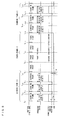
- FIG. 1 is a timing diagram showing a vertical sync signal, an operating state, and a waveform of a power supply current of the display device 1 .
- a single high-speed scanning period and a single pause period are set to two consecutive frames, for example, a frame between t 1 — 1 and t 1 — 3 and a frame between t 1 — 3 and t 1 — 4 , respectively.
- the display device 1 is different from the display device described in Patent Literature 1 in that, instead of setting a scanning period set to an entire period of a preceding one (hereinafter also simply referred to as “preceding frame”) of the two consecutive frames, the scanning period is speeded up so that the pause period is further set to a remaining period, which follows the end of the scanning period, in the preceding one of the two frames.
- the pause period is set to an entire period of a subsequent one (hereinafter also simply referred to as “subsequent frame”) of the two frames.
- a frame that includes a scanning period is called a scanning frame
- a frame that does not include a scanning period is called a pause frame.
- a scanning period (high-speed scanning period) is set to a period between t 1 — 1 and t 1 — 2 in the preceding frame
- a pause period is set to a period between t 1 — 2 and t 1 — 3 in the preceding frame.
- the pause period is also set to an entire period of the subsequent frame.
- a scanning period (high-speed scanning period) is set to a period between t 1 — 4 and t 1 — 5 in the preceding frame
- a pause period is set to a period between t 1 — 5 and t 1 — 6 in the preceding frame.
- the pause period is also set to an entire period of the subsequent frame.
- the display device 1 is configured such that, first, instead of setting a scanning period to an entire period of a preceding frame out of two consecutive frames, the scanning period is speeded up so that a pause period is set to a remaining period, which follows the end of the scanning period, in the preceding frame.
- the pause period is further set to an entire period of a subsequent frame out of the two consecutive frames.
- the display device 1 allows the display device 1 to have a significant increase in ratio of the pause period to the scanning period in an entire period of the two consecutive frames, as compared with the display device described in Patent Literature 1 and the comparative configuration of the display device.
- This makes it possible to more effectively stop or suppress generation of a self-consumed electric current which is consumed by the scanning line drive circuit 4 and the signal line drive circuit 6 for driving the scanning signal lines G and the data signal lines S of the display panel 2 , the power supply circuit 14 for supplying electric power to the scanning line drive circuit 4 and the signal line drive circuit 6 , and the like.
- a reduction in value I 12 of the self-consumed electric current in the pause period which is sufficiently long, allows a significant reduction in value I 11 of an average consumed electric current relative to a ground potential GND. This allows a significant reduction in electric power consumption of the display device 1 .
- a ratio of the scanning period to the pause period in the entire period of the two consecutive frames can be significantly reduced as compared with the display device described in Patent Literature 1 and the comparative configuration of the display device. This makes it possible to prevent degradation of display quality caused by generation of a luminance gradient. This point will be described later as well as the principle by which a luminance gradient is generated.
- FIG. 4 is a timing diagram showing a vertical sync signal and an operating state of a display device according to Embodiment 2 of the present invention.
- the display device according to Embodiment 2 of the present invention has the same configuration as that of the display device 1 of Embodiment 1 illustrated in FIG. 2 .
- the following description will discuss a difference between the display device according to Embodiment 2 and the display device 1 of Embodiment 1.
- a single high-speed scanning period and a single pause period are set to two consecutive frames, for example, to a frame between T 4 — 1 and T 4 — 3 and a frame between T 4 — 3 and T 4 — 4 , respectively.
- the display device 1 is configured such that, instead of setting the scanning period to an entire period of a preceding frame out of the two consecutive frames, the scanning period is speeded up so that the pause period is further set to a remaining period that follows the end of the scanning period in the preceding frame.
- the pause period is set to an entire period of a subsequent frame out of the two frames.
- Embodiment 2 of the present invention The difference between Embodiment 2 of the present invention and Embodiment 1 is that the following relation is maintained between a high-speed scanning period Td and a pause period Ts in the two consecutive frames.
- Td ⁇ (1 ⁇ 2) ⁇ Ts [Math 1]
- a period between T 4 — 1 and T 4 — 2 is shorter than a half of a period between T 4 — 2 and T 4 — 4 .
- Embodiment 2 of the present invention it is possible to significantly reduce electric power consumption of the display device 1 as in Embodiment 1.
- FIG. 5 is a timing diagram showing a vertical sync signal, an operating state, and a source outputting state of a display device according to Embodiment 3 of the present invention.
- the display device of Embodiment 3 of the present invention has the same configuration as that of the display device 1 of Embodiment 1 as illustrated in FIG. 2 .
- the following description will discuss a difference between the display device of Embodiment 3 and the display device 1 of Embodiment 1.
- a single high-speed scanning period and a single pause period are set to two consecutive frames, for example, a frame between T 5 — 1 and T 5 — 3 and a frame between T 5 — 3 and T 5 — 4 , respectively.
- the display device 1 is configured such that, instead of setting the scanning period to an entire period of a preceding frame out of the two consecutive frames, the scanning period is speeded up so that the pause period is further set to a remaining period that follows the end of the scanning period in the preceding frame.
- the pause period is set to an entire period of a subsequent frame out of the two frames.
- Embodiment 3 combines source inversion driving, in which a positive data signal and a negative data signal are alternately supplied from the signal line drive circuit 6 to a single data signal line S by AC driving.
- the source outputting state is positive in the frame between T 5 — 1 and T 5 — 3 and the frame between T 5 — 3 and T 5 — 4 , which are two consecutive frames, and the source outputting state is negative in the frame between T 5 — 4 and T 5 — 6 and the frame between T 5 — 6 and T 5 — 7 , which are two consecutive frames.
- Embodiment 3 of the present invention it is possible to significantly reduce electric power consumption of the display device 1 as in Embodiment 1, and also to prevent degradation of display quality caused by generation of a luminance gradient.
- FIG. 6 is a timing diagram showing a vertical sync signal, an operating state, and a source outputting state of a display device according to Embodiment 4 of the present invention.
- the display device of Embodiment 4 of the present invention has the same configuration as that of the display device 1 of Embodiment 1 as illustrated in FIG. 2 .
- the following description will discuss a difference between the display device of Embodiment 4 and the display device 1 of Embodiment 1.
- a single high-speed scanning period and a single pause period are set to two consecutive frames, for example, a frame between T 6 — 1 and T 6 — 3 and a frame between T 6 — 3 and T 6 — 4 , respectively.
- the display device 1 is configured such that, instead of setting the scanning period to an entire period of a preceding frame out of the two consecutive frames, the scanning period is speeded up so that the pause period is further set to a remaining period that follows an end of the scanning period in the preceding frame.
- the pause period is set to an entire period of a subsequent frame out of the two frames.
- Embodiment 4 of the present invention differs from Embodiment 1 in that, like Embodiment 2, the following relation is maintained between a high-speed scanning period Td and a pause period Ts the two consecutive frames.
- Td ⁇ (1 ⁇ 2) ⁇ Ts [Math 2]
- a period between T 6 — 1 and T 6 — 2 is shorter than a half of a period between T 6 — 2 and T 6 — 4 .
- Embodiment 4 of the present invention combines source inversion driving, in which a positive data signal and a negative data signal are alternately supplied from the signal line drive circuit 6 to a single data signal line S by AC driving.
- the source outputting state is positive in the frame between T 6 — 1 and T 6 — 3 and the frame between T 6 — 3 and T 6 — 4 , which are two consecutive frames, and the source outputting state is negative in the frame between T 6 — 4 and T 6 — 6 and the frame between T 5 — 6 and T 5 — 7 , which are two consecutive frames.
- Embodiment 4 of the present invention it is possible to significantly reduce electric power consumption of the display device 1 as in Embodiment 1, and also to prevent degradation of display quality caused by generation of a luminance gradient.
- FIG. 7 is a timing diagram showing a vertical sync signal and an operating state of a display device according to Embodiment 5 of the present invention.
- the display device of Embodiment 5 of the present invention has the same configuration as that of the display device 1 of Embodiment 1 as illustrated in FIG. 2 .
- the following description will discuss a difference between the display device of Embodiment 5 and the display device 1 of Embodiment 1.
- a single high-speed scanning period and a single pause period are set to two consecutive frames, for example, a frame between T 7 — 1 and T 7 — 3 and a frame between T 7 — 3 and T 7 — 4 , respectively.
- the display device 1 is configured such that, instead of setting the scanning period to an entire period of a preceding frame out of the two consecutive frames, the scanning period is speeded up so that the pause period is further set to a remaining period that follows an end of the scanning period in the preceding frame.
- the pause period is set to an entire period of a subsequent frame out of the two frames.
- Embodiment 5 of the present invention a driving frequency (refresh rate) is set to at least about 40 Hz in the two consecutive frames. That is, the difference is that the following relation is maintained between a high-speed scanning period Td and a pause period Ts. 1/( Td+Ts ) ⁇ 40 Hz [Math 3]
- a period between T 7 — 1 and T 7 — 4 is about 25 ms.
- Embodiment 5 of the present invention a ratio of a high-speed scanning period to two consecutive frames is not reduced. This makes it possible to reduce electric power consumption without causing flickering.
- FIG. 8 is a timing diagram showing a vertical sync signal, an operating state, and a waveform of a power supply current of a display device according to Embodiment 6 of the present invention.
- the display device of Embodiment 6 of the present invention has the same configuration as that of the display device 1 of Embodiment 1 as illustrated in FIG. 2 .
- the following description will discuss a difference between the display device of Embodiment 6 and the display device 1 of Embodiment 1.
- Embodiments 1 through 5 described above are configured such that a scanning frame and a pause frame are alternated.
- Embodiment 6 of the present invention is configured such that a plurality of consecutive pause frames follow a plurality of consecutive scanning frames. That is, (i) the plurality of consecutive scanning frames and (ii) the plurality of consecutive pause frames alternate with each other.
- a scanning frame is set between T 8 — 1 and T 8 — 3 , between T 8 — 3 and T 8 — 5 , and between T 8 — 5 and T 8 — 7 . That is, three scanning frames occur in succession.
- a pause frame is set between T 8 — 7 and T 8 — 8 , between T 8 — 8 and T 8 — 9 , between T 8 — 9 and T 8 — 10 , and between T 8 — 10 and T 8 — 11 . That is, four scanning frames occur in succession.
- a scanning frame is set between T 8 — 11 and T 8 — 13 , between T 8 — 13 and T 8 — 15 , and between T 8 — 15 and T 8 — 17 . That is, three scanning frames occur in succession.
- a focus on the scanning frame between T 8 — 5 and T 8 — 7 and the pause frame between T 8 — 7 and T 8 — 8 shows that similar descriptions as given in Embodiments 1 through 5 apply to Embodiment 5. That is, first, instead of setting the scanning period in an entire period of a preceding frame (the scanning frame between T 8 — 5 and T 8 — 7 ) of these two consecutive frames, the scanning period is speeded up so that a pause period is set to a remaining period, which follows an end of the scanning period, in the preceding frame. The pause period is further set in an entire period of a subsequent frame (the pause frame between T 8 — 7 and T 8 — 8 ).
- a reduction in value I 82 of a self-consumed electric current in the pause period which follows an end of the scanning period and is sufficiently long, allows a significant reduction in value I 81 of an average consumed electric current relative to a ground potential GND. This allows a significant reduction in electric power consumption of the display device 1 .
- Embodiment 6 of the present invention where a plurality of consecutive pause frames follow a plurality of consecutive scanning frames, it is possible to significantly reduce electric power consumption of the display device 1 as in Embodiment 1, and also to prevent degradation of display quality caused by generation of a luminance gradient.
- FIG. 9 is a timing diagram showing a vertical sync signal, an operating state, and a waveform of a power supply current of a display device according to Embodiment 7 of the present invention.
- the display device of Embodiment 7 of the present invention has the same configuration as that of the display device 1 of Embodiment 1 as illustrated in FIG. 2 .
- the following description will discuss a difference between the display device of Embodiment 7 and the display device 1 of Embodiment 1.
- Embodiment 7 of the present invention is configured similarly as Embodiment 6 such that a plurality of consecutive pause frames follow a plurality of consecutive scanning frames. That is, (i) the plurality of consecutive scanning frames and (ii) the plurality of consecutive pause frames alternate with each other.
- a scanning frame is set between T 9 — 1 and T 9 — 3 , between T 9 — 3 and T 9 — 5 , and between T 9 — 5 and T 9 — 7 . That is, three scanning frames occur in succession.
- a pause frame is set between T 9 — 7 and T 9 — 8 , between T 9 — 8 and T 9 — 9 , between T 9 — 9 and T 9 — 10 , and between T 9 — 10 and T 9 — 11 . That is, four scanning frames occur in succession.
- a scanning frame is set between T 9 — 11 and T 9 — 13 , between T 9 — 13 and T 9 — 15 , and between T 9 — 15 and T 9 — 17 . That is, three scanning frames occur in succession.
- a focus on the pause frame between T 9 — 10 and T 9 — 11 and the scanning frame between T 9 — 11 and T 9 — 13 shows that, unlike Embodiments 1 through 6, first, a pause period is set to an entire period of a preceding frame (the pause frame between T 9 — 10 and T 9 — 11 ) of these two consecutive frames. Further, a pause period (between T 9 — 11 and T 9 — 12 ) is set first to a subsequent frame (the scanning frame between T 9 — 11 and T 9 — 13 ), and a high-speed scanning period (between T 9 — 12 and T 9 — 13 ) is set to a remaining period, which follows an end of the pause period, in the subsequent frame.
- a reduction in value I 92 of a self-consumed electric current in the pause period which precedes an end of the scanning period and is sufficiently long, allows a significant reduction in value I 91 of an average consumed electric current relative to a ground potential GND. This allows a significant reduction in electric power consumption of the display device 1 .
- Embodiment 7 of the present invention where a plurality of consecutive pause frames follow a plurality of consecutive scanning frames, it is possible to significantly reduce electric power consumption of the display device 1 as in Embodiment 1, and also to prevent degradation of display quality caused by generation of a luminance gradient.
- FIG. 10 is a timing diagram showing a vertical sync signal, an operating state, a waveform of a power supply current, and a scanning signal of the display device 1 according to Embodiments 1 through 7 of the present invention.
- a single high-speed scanning period and a single pause period are set to two consecutive frames, for example, a frame between T 10 — 1 and T 10 — 3 and a frame between T 10 — 3 and T 10 — 4 , respectively.
- the pause period is set to a remaining period, which follows an end of the scanning period, in the preceding frame. Further, the pause period is set to an entire period of a subsequent frame out of the two frames.
- the vertical sync control signal is supplied for each high-speed scanning period.
- the control signal outputting section 12 changes a voltage of an AMP_Enable signal from an L value to an H value in sync with the vertical sync control signal. This causes a change in state of analog amplifiers (not shown) of the signal line drive circuit 6 from a non-operating state to an operating state (normal state).
- the scanning line drive circuit 4 supplies the scanning signal to the first scanning signal line G in sync with the vertical sync control signal and the horizontal sync control signal. This causes a state of gates of TFTs of pixels which are connected to the first scanning signal line G to be an on-state.
- the signal line drive circuit 6 supplies, to each of the data signal lines S, the data signal via a corresponding analog amplifier, among the analog amplifiers in the signal line drive circuit 6 , which is connected to the each of the data signal lines S.
- This causes a voltage necessary for a display to be supplied to the each of the data signal lines S. Accordingly, the voltage necessary for a display is written, via the TFTs, to pixel electrodes. In a case where the writing is completed, the state of the gates of the TFTs of the pixels which are connected to the first scanning signal line G returns from the on-state to an off-state.
- the next horizontal sync control signal is inputted.
- Pixels which are connected to the second and later scanning signal lines G are subjected to the writing by a process similar to that by which the writing is carried out with respect to the pixels which are connected to the first scanning signal line G.
- a period during which the writing is thus carried out with respect to the pixels connected to all the N scanning signal lines G is referred to as a “writing period”.
- the writing period is a period identical to the high-speed scanning period.
- the AMP_Enable signal maintains the H value during the writing period.
- the control signal outputting section 12 changes a voltage of the AMP_Enable signal from the H value to the L value. This causes the state of the analog amplifiers in the signal line drive circuit 6 to be the non-operating state (have a lower performance).
- the next vertical sync control signal is inputted.
- the second and later frames are driven by a process similar to the above process.
- each of the data signal lines S and an output of a corresponding one of the analog amplifiers in the signal line drive circuit 6 may be disconnected from each other.
- a gate of a TFT of each of the pixels included in the display panel 2 is, as described above, switched between an on-state and an off-state.
- a liquid crystal capacitor and a storage capacitor which are connected to each of the TFTs are charged by the switching between an on-state and an off-state of the gate of the each of the TFTs.
- FIG. 11 shows an equivalent circuit of one pixel.
- a pixel 100 is provided corresponding to an intersection between a gate line Gj and a source line Si.
- the pixel 100 includes a TFT 101 , a liquid crystal capacitor Clc, and a storage capacitor Ccs.
- the pixel 100 further includes a parasitic capacitance such as a capacitance Cgd formed between a drain electrode 102 and the gate line Gj.
- a gate, a source, and a drain of the TFT 101 are connected to the gate line Gj, the source line Si, and the drain electrode 102 , respectively.
- the liquid crystal capacitor Clc is formed by a liquid crystal layer provided between the drain electrode 102 and a common electrode to which a voltage COM is applied.
- the storage capacitor Ccs is formed by an insulating film provided between (i) the drain electrode 102 or an electrode connected to the drain electrode 102 and (ii) a storage capacitor bus line to which a voltage CS is applied.
- the voltage CS is, for example, equal to the voltage COM, but may have other voltage values.
- An electric potential of the drain electrode 102 is first charged with a source voltage supplied from the source line Si via the TFT 101 . Then, the electric potential of the drain electrode 102 changes in accordance with a change in voltage (Vgh ⁇ Vgl) on the gate line Gj via the parasitic capacitance Cgd. Further, since a parasitic capacitance Csd1 is formed, the electric potential of the drain electrode 102 also changes in accordance with a change in voltage caused by a reversal of polarity of the source line Si.
- ⁇ C, ⁇ Vg, and ⁇ Vs are calculated from the following formulae (3) through (5).
- [Math 5] ⁇ C ⁇ Clc+Ccs+Cgd+Csd 1 +Csd 2 (3) ⁇ Vg
- (4) ⁇ Vs
- Vgh, Vgl, Vsh, and Vsl are as follows. [Math 6]
- the electric potential of the drain electrode 102 is affected by the parasitic capacitance Csd2 as well as by the parasitic capacitance Csd1.
- an absolute value of an influence of the parasitic capacitance Csd2 on the drain electrode 102 is not so large enough to affect a luminance gradient, and is therefore ignored.
- the amounts of change in electric potential of the drain electrode 102 expressed by the formulae (1) and (2) are each called a feed-through voltage.
- Such feed-through voltages cause generation of a luminance gradient.
- a drain electrode is charged with a drain voltage, via a TFT of each pixel, by a data signal supplied from the signal line drive circuit 6 . Then, the drain voltage is caused to change by the feed-through voltages due to a fall of a scanning signal and a reversal of polarity of the data signal.
- a timing at which a change in drain voltage is caused by the reversal of polarity of the data signal varies between the first line and the m-th line.
- an effective voltage applied to liquid crystal is lower on the m-th line.
- a gradient of the voltage applied to the liquid crystal is generated along a scanning direction of the scanning line drive circuit 4 . This leads to a luminance gradient.
- the effect of preventing degradation of display quality caused by generation of a luminance gradient is exhibited by the present invention the most notably in a case where source inversion driving illustrated in (a) and (b) of FIG. 14 is used.
- the present invention exhibits the effect of reducing electric power consumption also in a case where dot inversion driving illustrated in (a) of FIG. 15 is used and in a case where line inversion driving illustrated in (b) of FIG. 15 is used.
- FIGS. 14 and 15 is a structural diagram illustrating a structure of the scanning signal lines G, the data signal lines S, and the pixel electrodes of the display panel 2 .
- (a) of each of FIGS. 14 and 15 illustrates polarities of voltages applied to the pixel electrodes in the n-th frame.
- (b) of each of FIGS. 14 and 15 illustrates polarities of voltages which are applied to the pixel electrodes in a subsequent frame (the (n+1)-th frame) and are reverse in polarity to the voltages applied in the n-th frame.
- the polarities of the voltages applied to the pixel electrodes are indicated by + (plus) and ⁇ (minus) shown in each of FIGS. 14 and 15 .
- FIG. 14 illustrates an example of the source inversion.
- the source inversion polarities of voltages to be applied are reversed for each of the data signal lines (source lines) S. This makes it possible to reverse the polarities of the voltages for every pixel electrodes arranged in the direction in which the scanning signal lines G extend (see (a) of FIG. 14 ).
- FIG. 14 also illustrates the source inversion identical to that illustrated in (a) of FIG. 14 .
- (b) of FIG. 14 is different from (a) of FIG. 14 in arrangement of the pixel electrodes.
- pixel electrodes connected to each of the data signal lines S are provided on one side of the each of the data signal lines S (on the right side in the example illustrated in (a) of FIG. 14 ).
- the pixel electrodes connected to each of the data signal lines S are provided in a zigzag pattern with respect to the each of the data signal lines S.
- the polarities of the voltages applied to pixel electrodes provided between adjacent ones of the data signal lines S are identical in the case of the arrangement illustrated in (a) of FIG. 14 .
- the polarities of the voltages applied to the pixel electrodes provided between adjacent ones of the data signal lines S alternate in the case of the arrangement illustrated in (b) of FIG. 14 .
- FIG. 15 illustrates an example of the line inversion.
- the line inversion polarities of voltages applied to the data signal lines S are reversed for each of the scanning signal lines G to be driven (for each of horizontal scanning periods). This makes it possible to reverse the polarities of the voltages for every pixel electrodes arranged in the direction in which the data signal lines S extend.
- FIG. 15 illustrates an example of the dot inversion.
- the dot inversion can be carried out by combining the source inversion illustrated in (a) of FIG. 14 and the line inversion illustrated in (a) of FIG. 15 .
- a voltage applied to the first data signal line S is set to have a plus (+) polarity, and then polarities of voltages applied to the second and later data signal lines S are sequentially reversed.
- the second scanning signal line G 2 a voltage applied to the first data signal line S is set to have a minus ( ⁇ ) polarity, and then polarities of voltages applied to the second and later data signal lines S are sequentially reversed.
- a transistor of the display panel 2 be a TFT having a semiconductor layer made from what is called “an oxide semiconductor.”
- the oxide semiconductor include IGZO (InGaZnOx).
- FIG. 17 shows respective characteristics of a TFT made from the oxide semiconductor, a TFT made from a-Si (amorphous silicon), and a TFT made from LTPS (Low Temperature Poly Silicon).
- a horizontal axis (Vg) indicates a gate voltage supplied to each of the TFTs
- a vertical axis (Id) indicates an electric current between a source and a drain of each of the TFTs.
- a period indicated as “TFT-on” is a period during which the TFTs are in an on-state
- a period indicated as “TFT-off” is a period during which the TFTs are in an off-state.
- a value of the electric current (i.e., electron mobility) of the TFT made from the oxide semiconductor is greater than that of the TFT made from a-Si.
- the TFT made from a-Si has an electric current Id of 1 uA in an on-state (at “TFT-on”), whereas the TFT made from the oxide semiconductor has an electric current Id of 20 uA to 50 uA at TFT-on.
- the value of the electric current (electron mobility) of the TFT made from the oxide semiconductor is 20 to 50 times greater than that of the TFT made from a-Si.
- the TFT made from the oxide semiconductor thus has an excellent ON characteristic.
- the TFT made from the oxide semiconductor is used for each of the pixels as the transistor of the display panel 2 , the TFT of the each of the pixels has an excellent ON characteristic. This increases electron mobility at the time of writing pixel data to each of the pixels. Accordingly, time required to write the pixel data to each of the pixels can be further reduced.
- Td is a length of the scanning period and Ts is a sum of a length of the pause period set to the preceding frame and a length of the pause period set to the subsequent frame.
- Td ⁇ (1 ⁇ 2) ⁇ Ts [Math 7]
- the following formula is preferably met. 1/( Td+Ts ) ⁇ 40 Hz [Math 8]
- a polarity of a voltage of a data signal supplied to the display panel is preferably reversed for each scanning period.
- a pause period is preferably set to an entire period of each of a plurality of consecutive frames which follow the subsequent frame.
- the display device further includes a memory in which a video signal supplied from outside the display device is tentatively stored.
- a video signal is transmitted from the main device, which is provided outside the display device, to, for example, the timing controller of the display device.
- the main device transmits a video signal to the timing controller
- the main device owing to the provision of the memory, does not have to convert the video signal into a signal having a speed in accordance with scanning carried out by the display device.
- the main device can use the same circuit configuration as that in a conventional technique, without the need to include a special circuit which is separately provided in accordance with a speed of the scanning carried out by the display device.
- the display device according to the embodiment of the present invention be a liquid crystal display device.
- the display panel include a data signal line, a scanning signal line, a pixel electrode, and a transistor which is connected with the data signal line, the scanning signal line, and the pixel electrode and (ii) the transistor have a semiconductor layer which is made from an oxide semiconductor.
- the oxide semiconductor be IGZO.
- the display device may include a liquid crystal display panel or an organic electroluminescent display panel so that the display device is provided as a liquid crystal display device or an organic EL display device.
- a display device can be widely used as various display devices such as a liquid crystal display device, an organic EL display device, and an electronic paper.
Abstract
Description
- Japanese Patent Application Publication, Tokukai, No. 2001-312253 A (Publication Date: Nov. 9, 2001)
Td≦(½)·Ts [Math 1]
Td≦(½)·Ts [Math 2]
1/(Td+Ts)≧40 Hz [Math 3]
[Math 4]
ΔVgd=(Cgd/ΣC)*ΔVg (1)
ΔVsd1=(Csd1/ΣC)*ΔVs (2)
[Math 5]
ΣC≈Clc+Ccs+Cgd+Csd1+Csd2 (3)
ΔVg=|Vgh−Vgl| (4)
ΔVs=|Vsh−Vsl| (5)
[Math 6]
Td≦(½)·Ts [Math 7]
1/(Td+Ts)≧40 Hz [Math 8]
- 1: display device
- 2: display panel
- 4: scanning line drive circuit
- 6: signal line drive circuit
- 8: common electrode drive circuit
- 10: timing controller
- 12: control signal outputting section
- 14: power supply circuit
- 16: memory
- G: scanning signal line
- S: data signal line
Claims (20)
Td≦(½)·Ts
1/(Td+Ts)≧40 Hz.
Td≦(½)·Ts
1/(Td+Ts)≧40 Hz
Applications Claiming Priority (3)
| Application Number | Priority Date | Filing Date | Title |
|---|---|---|---|
| JP2011-085812 | 2011-04-07 | ||
| JP2011085812 | 2011-04-07 | ||
| PCT/JP2012/059035 WO2012137756A1 (en) | 2011-04-07 | 2012-04-03 | Display device, and method for driving same |
Publications (2)
| Publication Number | Publication Date |
|---|---|
| US20140028646A1 US20140028646A1 (en) | 2014-01-30 |
| US9293103B2 true US9293103B2 (en) | 2016-03-22 |
Family
ID=46969153
Family Applications (1)
| Application Number | Title | Priority Date | Filing Date |
|---|---|---|---|
| US14/009,340 Active US9293103B2 (en) | 2011-04-07 | 2012-04-03 | Display device, and method for driving same |
Country Status (3)
| Country | Link |
|---|---|
| US (1) | US9293103B2 (en) |
| TW (1) | TWI537926B (en) |
| WO (1) | WO2012137756A1 (en) |
Cited By (2)
| Publication number | Priority date | Publication date | Assignee | Title |
|---|---|---|---|---|
| US20150170599A1 (en) * | 2012-06-01 | 2015-06-18 | Sharp Kabushiki Kaisha | Method of driving display device, display device, and portable device including the same |
| US20160196789A1 (en) * | 2012-12-27 | 2016-07-07 | Sharp Kabushiki Kaisha | Liquid crystal display device and driving method therefor |
Families Citing this family (6)
| Publication number | Priority date | Publication date | Assignee | Title |
|---|---|---|---|---|
| WO2013118652A1 (en) * | 2012-02-10 | 2013-08-15 | シャープ株式会社 | Display device and drive method therefor |
| CN104781871B (en) * | 2012-11-20 | 2017-06-13 | 夏普株式会社 | Liquid crystal display device and its driving method |
| JP6185998B2 (en) * | 2013-08-23 | 2017-08-23 | シャープ株式会社 | Liquid crystal display |
| US10497330B2 (en) * | 2015-12-02 | 2019-12-03 | Sharp Kabushiki Kaisha | Display device that performs pause driving |
| KR102518922B1 (en) * | 2016-01-21 | 2023-04-07 | 삼성디스플레이 주식회사 | Display device and method of driving the same |
| CN108665844B (en) * | 2018-05-21 | 2021-05-14 | 京东方科技集团股份有限公司 | Display device, driving method thereof and driving device thereof |
Citations (22)
| Publication number | Priority date | Publication date | Assignee | Title |
|---|---|---|---|---|
| JP2001312253A (en) | 2000-04-28 | 2001-11-09 | Sharp Corp | Driving method for display device and display device using the same and portable equipment |
| US20020041281A1 (en) * | 2000-10-06 | 2002-04-11 | Toshihiro Yanagi | Active matrix type display and a driving method thereof |
| US20020180673A1 (en) * | 2000-04-28 | 2002-12-05 | Kazuhiho Tsuda | Display device method of driving same and electronic device mounting same |
| US20040145551A1 (en) * | 2003-01-29 | 2004-07-29 | Mitsubishi Denki Kabushiki Kaisha | Liquid crystal display apparatus having pixels with low leakage current |
| US20040233228A1 (en) * | 2003-03-24 | 2004-11-25 | Yusuke Ota | Display system, data driver, and display drive method |
| US20050104831A1 (en) | 2003-11-14 | 2005-05-19 | Masafumi Hoshino | TFT liquid crystal display driving method and TFT liquid crystal display driving module |
| US20060007092A1 (en) * | 2004-06-16 | 2006-01-12 | Hitachi Displays, Ltd. | Liquid-crystal display device and method of driving liquid-crystal display device |
| US20060103637A1 (en) * | 2004-10-29 | 2006-05-18 | Sony Corporation | Inputting/outputting apparatus and method, recording medium, and program |
| US20070273683A1 (en) * | 2004-07-14 | 2007-11-29 | Takaharu Yamada | Active Matrix Substrate and Drive Circuit Thereof |
| US20080297500A1 (en) | 2007-05-30 | 2008-12-04 | Hirofumi Kato | Display device and method of driving the same |
| US20090122172A1 (en) * | 2007-11-13 | 2009-05-14 | Canon Kabushiki Kaisha | Solid-state imaging apparatus |
| US20100065840A1 (en) | 2008-09-12 | 2010-03-18 | Semiconductor Energy Laboratory Co., Ltd. | Display device |
| US20100073341A1 (en) * | 2008-09-19 | 2010-03-25 | Seiko Epson Corporation | Electro-optical device, driving method thereof, and electronic apparatus |
| US20100103156A1 (en) * | 2008-10-29 | 2010-04-29 | Sony Corporation | Image display apparatus and method of driving the image display apparatus |
| US20100277463A1 (en) * | 2009-04-29 | 2010-11-04 | Shih-Chieh Yen | Timing controller with power-saving function |
| US20110175883A1 (en) * | 2010-01-20 | 2011-07-21 | Semiconductor Energy Laboratory Co., Ltd. | Driving method of liquid crystal display device |
| US20110181560A1 (en) * | 2010-01-24 | 2011-07-28 | Semiconductor Energy Laboratory Co., Ltd. | Display device |
| US20110180794A1 (en) * | 2010-01-24 | 2011-07-28 | Semiconductor Energy Laboratory Co., Ltd. | Display device |
| US20130009935A1 (en) * | 2010-03-03 | 2013-01-10 | Sharp Kabushiki Kaisha | Display device, method for driving same, and liquid crystal display device |
| US20130050146A1 (en) * | 2010-05-21 | 2013-02-28 | Kohji Saitoh | Display device and method of driving the same, and display system |
| US20130314360A1 (en) * | 2011-04-15 | 2013-11-28 | Sharp Kabushiki Kaisha | Display device, method for driving display device, and electronic equipment |
| US20140191989A1 (en) * | 2011-04-07 | 2014-07-10 | Sharp Kabushiki Kaisha | Electronic apparatus, and method for controlling electronic apparatus |
Family Cites Families (1)
| Publication number | Priority date | Publication date | Assignee | Title |
|---|---|---|---|---|
| JP4487024B2 (en) * | 2002-12-10 | 2010-06-23 | 株式会社日立製作所 | Method for driving liquid crystal display device and liquid crystal display device |
-
2012
- 2012-04-03 WO PCT/JP2012/059035 patent/WO2012137756A1/en active Application Filing
- 2012-04-03 US US14/009,340 patent/US9293103B2/en active Active
- 2012-04-06 TW TW101112366A patent/TWI537926B/en not_active IP Right Cessation
Patent Citations (26)
| Publication number | Priority date | Publication date | Assignee | Title |
|---|---|---|---|---|
| JP2001312253A (en) | 2000-04-28 | 2001-11-09 | Sharp Corp | Driving method for display device and display device using the same and portable equipment |
| US20020180673A1 (en) * | 2000-04-28 | 2002-12-05 | Kazuhiho Tsuda | Display device method of driving same and electronic device mounting same |
| US20080055218A1 (en) | 2000-04-28 | 2008-03-06 | Sharp Kabushiki Kaisha | Display device, method of driving same and electronic device mounting same |
| US20020041281A1 (en) * | 2000-10-06 | 2002-04-11 | Toshihiro Yanagi | Active matrix type display and a driving method thereof |
| US20040145551A1 (en) * | 2003-01-29 | 2004-07-29 | Mitsubishi Denki Kabushiki Kaisha | Liquid crystal display apparatus having pixels with low leakage current |
| US20040233228A1 (en) * | 2003-03-24 | 2004-11-25 | Yusuke Ota | Display system, data driver, and display drive method |
| US20050104831A1 (en) | 2003-11-14 | 2005-05-19 | Masafumi Hoshino | TFT liquid crystal display driving method and TFT liquid crystal display driving module |
| JP2005148362A (en) | 2003-11-14 | 2005-06-09 | Seiko Instruments Inc | Method for driving tft liquid crystal panel and tft liquid crystal panel driving module |
| US20060007092A1 (en) * | 2004-06-16 | 2006-01-12 | Hitachi Displays, Ltd. | Liquid-crystal display device and method of driving liquid-crystal display device |
| US20070273683A1 (en) * | 2004-07-14 | 2007-11-29 | Takaharu Yamada | Active Matrix Substrate and Drive Circuit Thereof |
| US20060103637A1 (en) * | 2004-10-29 | 2006-05-18 | Sony Corporation | Inputting/outputting apparatus and method, recording medium, and program |
| JP2008298997A (en) | 2007-05-30 | 2008-12-11 | Toshiba Matsushita Display Technology Co Ltd | Display, and driving method for display |
| US20080297500A1 (en) | 2007-05-30 | 2008-12-04 | Hirofumi Kato | Display device and method of driving the same |
| US20090122172A1 (en) * | 2007-11-13 | 2009-05-14 | Canon Kabushiki Kaisha | Solid-state imaging apparatus |
| US20100065840A1 (en) | 2008-09-12 | 2010-03-18 | Semiconductor Energy Laboratory Co., Ltd. | Display device |
| JP2010092036A (en) | 2008-09-12 | 2010-04-22 | Semiconductor Energy Lab Co Ltd | Display device |
| US20100073341A1 (en) * | 2008-09-19 | 2010-03-25 | Seiko Epson Corporation | Electro-optical device, driving method thereof, and electronic apparatus |
| US20100103156A1 (en) * | 2008-10-29 | 2010-04-29 | Sony Corporation | Image display apparatus and method of driving the image display apparatus |
| US20100277463A1 (en) * | 2009-04-29 | 2010-11-04 | Shih-Chieh Yen | Timing controller with power-saving function |
| US20110175883A1 (en) * | 2010-01-20 | 2011-07-21 | Semiconductor Energy Laboratory Co., Ltd. | Driving method of liquid crystal display device |
| US20110181560A1 (en) * | 2010-01-24 | 2011-07-28 | Semiconductor Energy Laboratory Co., Ltd. | Display device |
| US20110180794A1 (en) * | 2010-01-24 | 2011-07-28 | Semiconductor Energy Laboratory Co., Ltd. | Display device |
| US20130009935A1 (en) * | 2010-03-03 | 2013-01-10 | Sharp Kabushiki Kaisha | Display device, method for driving same, and liquid crystal display device |
| US20130050146A1 (en) * | 2010-05-21 | 2013-02-28 | Kohji Saitoh | Display device and method of driving the same, and display system |
| US20140191989A1 (en) * | 2011-04-07 | 2014-07-10 | Sharp Kabushiki Kaisha | Electronic apparatus, and method for controlling electronic apparatus |
| US20130314360A1 (en) * | 2011-04-15 | 2013-11-28 | Sharp Kabushiki Kaisha | Display device, method for driving display device, and electronic equipment |
Non-Patent Citations (1)
| Title |
|---|
| Official Communication issued in International Patent Application No. PCT/JP2012/059035, mailed on May 15, 2012. |
Cited By (3)
| Publication number | Priority date | Publication date | Assignee | Title |
|---|---|---|---|---|
| US20150170599A1 (en) * | 2012-06-01 | 2015-06-18 | Sharp Kabushiki Kaisha | Method of driving display device, display device, and portable device including the same |
| US9659543B2 (en) * | 2012-06-01 | 2017-05-23 | Sharp Kabushiki Kaisha | Method of driving liquid crystal display device during write period |
| US20160196789A1 (en) * | 2012-12-27 | 2016-07-07 | Sharp Kabushiki Kaisha | Liquid crystal display device and driving method therefor |
Also Published As
| Publication number | Publication date |
|---|---|
| TW201248602A (en) | 2012-12-01 |
| US20140028646A1 (en) | 2014-01-30 |
| WO2012137756A1 (en) | 2012-10-11 |
| TWI537926B (en) | 2016-06-11 |
Similar Documents
| Publication | Publication Date | Title |
|---|---|---|
| US9293103B2 (en) | Display device, and method for driving same | |
| JP6105026B2 (en) | Driving device and display device | |
| JP5837177B2 (en) | Driving device and display device | |
| US9311872B2 (en) | Display device with timing controller | |
| US9633617B2 (en) | Liquid crystal display device with drive control circuit and method for driving same | |
| TWI536339B (en) | Display device and driving method thereof | |
| US9177517B2 (en) | Display device and drive method therefor | |
| US9299305B2 (en) | Display device and drive method therefor | |
| US9934743B2 (en) | Drive device, drive method, display device and display method | |
| WO2012133281A1 (en) | Display device | |
| US9412324B2 (en) | Drive device and display device | |
| US9165516B2 (en) | Display device and drive method therefor | |
| US9805673B2 (en) | Method of driving a display panel and display device performing the same | |
| US9349338B2 (en) | Display device and method for driving same | |
| WO2013024776A1 (en) | Display device and drive method for same | |
| US20150022509A1 (en) | Display device and drive method therefor | |
| KR102629152B1 (en) | Liquid crystal display device and method of driving the same | |
| KR101785339B1 (en) | Common voltage driver and liquid crystal display device including thereof | |
| US9626920B2 (en) | Liquid crystal display device and method for driving same | |
| JP2009205044A (en) | Electrooptical device, drive circuit, and electronic equipment | |
| JP2010026412A (en) | Electrooptical apparatus, method of driving the same, and electronic device |
Legal Events
| Date | Code | Title | Description |
|---|---|---|---|
| AS | Assignment |
Owner name: SHARP KABUSHIKI KAISHA, JAPAN Free format text: ASSIGNMENT OF ASSIGNORS INTEREST;ASSIGNORS:SAITOH, KOHJI;YAMATO, ASAHI;OZAKI, MASAMI;AND OTHERS;SIGNING DATES FROM 20130919 TO 20130925;REEL/FRAME:031327/0368 |
|
| STCF | Information on status: patent grant |
Free format text: PATENTED CASE |
|
| MAFP | Maintenance fee payment |
Free format text: PAYMENT OF MAINTENANCE FEE, 4TH YEAR, LARGE ENTITY (ORIGINAL EVENT CODE: M1551); ENTITY STATUS OF PATENT OWNER: LARGE ENTITY Year of fee payment: 4 |
|
| MAFP | Maintenance fee payment |
Free format text: PAYMENT OF MAINTENANCE FEE, 8TH YEAR, LARGE ENTITY (ORIGINAL EVENT CODE: M1552); ENTITY STATUS OF PATENT OWNER: LARGE ENTITY Year of fee payment: 8 |