US9281371B2 - Super-self-aligned contacts and method for making the same - Google Patents
Super-self-aligned contacts and method for making the same Download PDFInfo
- Publication number
- US9281371B2 US9281371B2 US14/566,249 US201414566249A US9281371B2 US 9281371 B2 US9281371 B2 US 9281371B2 US 201414566249 A US201414566249 A US 201414566249A US 9281371 B2 US9281371 B2 US 9281371B2
- Authority
- US
- United States
- Prior art keywords
- gate structure
- linear
- linear gate
- hard mask
- contact
- Prior art date
- Legal status (The legal status is an assumption and is not a legal conclusion. Google has not performed a legal analysis and makes no representation as to the accuracy of the status listed.)
- Expired - Fee Related
Links
- 238000000034 method Methods 0.000 title description 73
- 239000004065 semiconductor Substances 0.000 claims abstract description 44
- 239000000463 material Substances 0.000 claims description 55
- 238000010521 absorption reaction Methods 0.000 claims description 27
- 125000006850 spacer group Chemical group 0.000 claims description 11
- 239000003989 dielectric material Substances 0.000 claims 4
- 239000004020 conductor Substances 0.000 abstract description 7
- 229920002120 photoresistant polymer Polymers 0.000 description 110
- 238000005530 etching Methods 0.000 description 21
- 238000000151 deposition Methods 0.000 description 14
- 229910052751 metal Inorganic materials 0.000 description 14
- 239000002184 metal Substances 0.000 description 14
- 238000004519 manufacturing process Methods 0.000 description 13
- 238000005229 chemical vapour deposition Methods 0.000 description 7
- 239000000126 substance Substances 0.000 description 6
- 239000000758 substrate Substances 0.000 description 6
- ATJFFYVFTNAWJD-UHFFFAOYSA-N Tin Chemical compound [Sn] ATJFFYVFTNAWJD-UHFFFAOYSA-N 0.000 description 5
- 238000000059 patterning Methods 0.000 description 5
- 238000004380 ashing Methods 0.000 description 3
- 230000015572 biosynthetic process Effects 0.000 description 3
- 238000004132 cross linking Methods 0.000 description 3
- 238000007792 addition Methods 0.000 description 2
- 230000004075 alteration Effects 0.000 description 2
- 238000000206 photolithography Methods 0.000 description 2
- 238000005240 physical vapour deposition Methods 0.000 description 2
- 229910021332 silicide Inorganic materials 0.000 description 2
- FVBUAEGBCNSCDD-UHFFFAOYSA-N silicide(4-) Chemical compound [Si-4] FVBUAEGBCNSCDD-UHFFFAOYSA-N 0.000 description 2
- 229910012990 NiSi2 Inorganic materials 0.000 description 1
- 229910052581 Si3N4 Inorganic materials 0.000 description 1
- XUIMIQQOPSSXEZ-UHFFFAOYSA-N Silicon Chemical compound [Si] XUIMIQQOPSSXEZ-UHFFFAOYSA-N 0.000 description 1
- 239000002253 acid Substances 0.000 description 1
- 229910003481 amorphous carbon Inorganic materials 0.000 description 1
- 230000005540 biological transmission Effects 0.000 description 1
- 230000008021 deposition Effects 0.000 description 1
- 238000002955 isolation Methods 0.000 description 1
- 238000001465 metallisation Methods 0.000 description 1
- 229910021334 nickel silicide Inorganic materials 0.000 description 1
- RUFLMLWJRZAWLJ-UHFFFAOYSA-N nickel silicide Chemical compound [Ni]=[Si]=[Ni] RUFLMLWJRZAWLJ-UHFFFAOYSA-N 0.000 description 1
- 150000004767 nitrides Chemical class 0.000 description 1
- 229910021420 polycrystalline silicon Inorganic materials 0.000 description 1
- 229920000642 polymer Polymers 0.000 description 1
- 229920005591 polysilicon Polymers 0.000 description 1
- 238000011112 process operation Methods 0.000 description 1
- 229910052710 silicon Inorganic materials 0.000 description 1
- 239000010703 silicon Substances 0.000 description 1
- 229910052814 silicon oxide Inorganic materials 0.000 description 1
- WFKWXMTUELFFGS-UHFFFAOYSA-N tungsten Chemical compound [W] WFKWXMTUELFFGS-UHFFFAOYSA-N 0.000 description 1
- 229910052721 tungsten Inorganic materials 0.000 description 1
- 239000010937 tungsten Substances 0.000 description 1
Images


Classifications
-
- H—ELECTRICITY
- H01—ELECTRIC ELEMENTS
- H01L—SEMICONDUCTOR DEVICES NOT COVERED BY CLASS H10
- H01L27/00—Devices consisting of a plurality of semiconductor or other solid-state components formed in or on a common substrate
- H01L27/02—Devices consisting of a plurality of semiconductor or other solid-state components formed in or on a common substrate including semiconductor components specially adapted for rectifying, oscillating, amplifying or switching and having at least one potential-jump barrier or surface barrier; including integrated passive circuit elements with at least one potential-jump barrier or surface barrier
- H01L27/04—Devices consisting of a plurality of semiconductor or other solid-state components formed in or on a common substrate including semiconductor components specially adapted for rectifying, oscillating, amplifying or switching and having at least one potential-jump barrier or surface barrier; including integrated passive circuit elements with at least one potential-jump barrier or surface barrier the substrate being a semiconductor body
- H01L27/08—Devices consisting of a plurality of semiconductor or other solid-state components formed in or on a common substrate including semiconductor components specially adapted for rectifying, oscillating, amplifying or switching and having at least one potential-jump barrier or surface barrier; including integrated passive circuit elements with at least one potential-jump barrier or surface barrier the substrate being a semiconductor body including only semiconductor components of a single kind
- H01L27/085—Devices consisting of a plurality of semiconductor or other solid-state components formed in or on a common substrate including semiconductor components specially adapted for rectifying, oscillating, amplifying or switching and having at least one potential-jump barrier or surface barrier; including integrated passive circuit elements with at least one potential-jump barrier or surface barrier the substrate being a semiconductor body including only semiconductor components of a single kind including field-effect components only
- H01L27/088—Devices consisting of a plurality of semiconductor or other solid-state components formed in or on a common substrate including semiconductor components specially adapted for rectifying, oscillating, amplifying or switching and having at least one potential-jump barrier or surface barrier; including integrated passive circuit elements with at least one potential-jump barrier or surface barrier the substrate being a semiconductor body including only semiconductor components of a single kind including field-effect components only the components being field-effect transistors with insulated gate
- H01L27/092—Devices consisting of a plurality of semiconductor or other solid-state components formed in or on a common substrate including semiconductor components specially adapted for rectifying, oscillating, amplifying or switching and having at least one potential-jump barrier or surface barrier; including integrated passive circuit elements with at least one potential-jump barrier or surface barrier the substrate being a semiconductor body including only semiconductor components of a single kind including field-effect components only the components being field-effect transistors with insulated gate complementary MIS field-effect transistors
-
- H—ELECTRICITY
- H01—ELECTRIC ELEMENTS
- H01L—SEMICONDUCTOR DEVICES NOT COVERED BY CLASS H10
- H01L21/00—Processes or apparatus adapted for the manufacture or treatment of semiconductor or solid state devices or of parts thereof
- H01L21/70—Manufacture or treatment of devices consisting of a plurality of solid state components formed in or on a common substrate or of parts thereof; Manufacture of integrated circuit devices or of parts thereof
- H01L21/71—Manufacture of specific parts of devices defined in group H01L21/70
- H01L21/768—Applying interconnections to be used for carrying current between separate components within a device comprising conductors and dielectrics
- H01L21/76801—Applying interconnections to be used for carrying current between separate components within a device comprising conductors and dielectrics characterised by the formation and the after-treatment of the dielectrics, e.g. smoothing
- H01L21/76802—Applying interconnections to be used for carrying current between separate components within a device comprising conductors and dielectrics characterised by the formation and the after-treatment of the dielectrics, e.g. smoothing by forming openings in dielectrics
- H01L21/76816—Aspects relating to the layout of the pattern or to the size of vias or trenches
-
- H—ELECTRICITY
- H01—ELECTRIC ELEMENTS
- H01L—SEMICONDUCTOR DEVICES NOT COVERED BY CLASS H10
- H01L21/00—Processes or apparatus adapted for the manufacture or treatment of semiconductor or solid state devices or of parts thereof
- H01L21/70—Manufacture or treatment of devices consisting of a plurality of solid state components formed in or on a common substrate or of parts thereof; Manufacture of integrated circuit devices or of parts thereof
- H01L21/71—Manufacture of specific parts of devices defined in group H01L21/70
- H01L21/768—Applying interconnections to be used for carrying current between separate components within a device comprising conductors and dielectrics
- H01L21/76838—Applying interconnections to be used for carrying current between separate components within a device comprising conductors and dielectrics characterised by the formation and the after-treatment of the conductors
- H01L21/76877—Filling of holes, grooves or trenches, e.g. vias, with conductive material
- H01L21/76879—Filling of holes, grooves or trenches, e.g. vias, with conductive material by selective deposition of conductive material in the vias, e.g. selective C.V.D. on semiconductor material, plating
-
- H—ELECTRICITY
- H01—ELECTRIC ELEMENTS
- H01L—SEMICONDUCTOR DEVICES NOT COVERED BY CLASS H10
- H01L21/00—Processes or apparatus adapted for the manufacture or treatment of semiconductor or solid state devices or of parts thereof
- H01L21/70—Manufacture or treatment of devices consisting of a plurality of solid state components formed in or on a common substrate or of parts thereof; Manufacture of integrated circuit devices or of parts thereof
- H01L21/71—Manufacture of specific parts of devices defined in group H01L21/70
- H01L21/768—Applying interconnections to be used for carrying current between separate components within a device comprising conductors and dielectrics
- H01L21/76897—Formation of self-aligned vias or contact plugs, i.e. involving a lithographically uncritical step
-
- H—ELECTRICITY
- H01—ELECTRIC ELEMENTS
- H01L—SEMICONDUCTOR DEVICES NOT COVERED BY CLASS H10
- H01L21/00—Processes or apparatus adapted for the manufacture or treatment of semiconductor or solid state devices or of parts thereof
- H01L21/70—Manufacture or treatment of devices consisting of a plurality of solid state components formed in or on a common substrate or of parts thereof; Manufacture of integrated circuit devices or of parts thereof
- H01L21/77—Manufacture or treatment of devices consisting of a plurality of solid state components or integrated circuits formed in, or on, a common substrate
- H01L21/78—Manufacture or treatment of devices consisting of a plurality of solid state components or integrated circuits formed in, or on, a common substrate with subsequent division of the substrate into plural individual devices
- H01L21/82—Manufacture or treatment of devices consisting of a plurality of solid state components or integrated circuits formed in, or on, a common substrate with subsequent division of the substrate into plural individual devices to produce devices, e.g. integrated circuits, each consisting of a plurality of components
- H01L21/822—Manufacture or treatment of devices consisting of a plurality of solid state components or integrated circuits formed in, or on, a common substrate with subsequent division of the substrate into plural individual devices to produce devices, e.g. integrated circuits, each consisting of a plurality of components the substrate being a semiconductor, using silicon technology
- H01L21/8232—Field-effect technology
- H01L21/8234—MIS technology, i.e. integration processes of field effect transistors of the conductor-insulator-semiconductor type
- H01L21/823475—MIS technology, i.e. integration processes of field effect transistors of the conductor-insulator-semiconductor type interconnection or wiring or contact manufacturing related aspects
-
- H—ELECTRICITY
- H01—ELECTRIC ELEMENTS
- H01L—SEMICONDUCTOR DEVICES NOT COVERED BY CLASS H10
- H01L21/00—Processes or apparatus adapted for the manufacture or treatment of semiconductor or solid state devices or of parts thereof
- H01L21/70—Manufacture or treatment of devices consisting of a plurality of solid state components formed in or on a common substrate or of parts thereof; Manufacture of integrated circuit devices or of parts thereof
- H01L21/77—Manufacture or treatment of devices consisting of a plurality of solid state components or integrated circuits formed in, or on, a common substrate
- H01L21/78—Manufacture or treatment of devices consisting of a plurality of solid state components or integrated circuits formed in, or on, a common substrate with subsequent division of the substrate into plural individual devices
- H01L21/82—Manufacture or treatment of devices consisting of a plurality of solid state components or integrated circuits formed in, or on, a common substrate with subsequent division of the substrate into plural individual devices to produce devices, e.g. integrated circuits, each consisting of a plurality of components
- H01L21/822—Manufacture or treatment of devices consisting of a plurality of solid state components or integrated circuits formed in, or on, a common substrate with subsequent division of the substrate into plural individual devices to produce devices, e.g. integrated circuits, each consisting of a plurality of components the substrate being a semiconductor, using silicon technology
- H01L21/8232—Field-effect technology
- H01L21/8234—MIS technology, i.e. integration processes of field effect transistors of the conductor-insulator-semiconductor type
- H01L21/8238—Complementary field-effect transistors, e.g. CMOS
- H01L21/823807—Complementary field-effect transistors, e.g. CMOS with a particular manufacturing method of the channel structures, e.g. channel implants, halo or pocket implants, or channel materials
-
- H—ELECTRICITY
- H01—ELECTRIC ELEMENTS
- H01L—SEMICONDUCTOR DEVICES NOT COVERED BY CLASS H10
- H01L21/00—Processes or apparatus adapted for the manufacture or treatment of semiconductor or solid state devices or of parts thereof
- H01L21/70—Manufacture or treatment of devices consisting of a plurality of solid state components formed in or on a common substrate or of parts thereof; Manufacture of integrated circuit devices or of parts thereof
- H01L21/77—Manufacture or treatment of devices consisting of a plurality of solid state components or integrated circuits formed in, or on, a common substrate
- H01L21/78—Manufacture or treatment of devices consisting of a plurality of solid state components or integrated circuits formed in, or on, a common substrate with subsequent division of the substrate into plural individual devices
- H01L21/82—Manufacture or treatment of devices consisting of a plurality of solid state components or integrated circuits formed in, or on, a common substrate with subsequent division of the substrate into plural individual devices to produce devices, e.g. integrated circuits, each consisting of a plurality of components
- H01L21/822—Manufacture or treatment of devices consisting of a plurality of solid state components or integrated circuits formed in, or on, a common substrate with subsequent division of the substrate into plural individual devices to produce devices, e.g. integrated circuits, each consisting of a plurality of components the substrate being a semiconductor, using silicon technology
- H01L21/8232—Field-effect technology
- H01L21/8234—MIS technology, i.e. integration processes of field effect transistors of the conductor-insulator-semiconductor type
- H01L21/8238—Complementary field-effect transistors, e.g. CMOS
- H01L21/823828—Complementary field-effect transistors, e.g. CMOS with a particular manufacturing method of the gate conductors, e.g. particular materials, shapes
-
- H—ELECTRICITY
- H01—ELECTRIC ELEMENTS
- H01L—SEMICONDUCTOR DEVICES NOT COVERED BY CLASS H10
- H01L23/00—Details of semiconductor or other solid state devices
- H01L23/48—Arrangements for conducting electric current to or from the solid state body in operation, e.g. leads, terminal arrangements ; Selection of materials therefor
- H01L23/481—Internal lead connections, e.g. via connections, feedthrough structures
-
- H—ELECTRICITY
- H01—ELECTRIC ELEMENTS
- H01L—SEMICONDUCTOR DEVICES NOT COVERED BY CLASS H10
- H01L27/00—Devices consisting of a plurality of semiconductor or other solid-state components formed in or on a common substrate
- H01L27/02—Devices consisting of a plurality of semiconductor or other solid-state components formed in or on a common substrate including semiconductor components specially adapted for rectifying, oscillating, amplifying or switching and having at least one potential-jump barrier or surface barrier; including integrated passive circuit elements with at least one potential-jump barrier or surface barrier
- H01L27/0203—Particular design considerations for integrated circuits
- H01L27/0207—Geometrical layout of the components, e.g. computer aided design; custom LSI, semi-custom LSI, standard cell technique
-
- H—ELECTRICITY
- H01—ELECTRIC ELEMENTS
- H01L—SEMICONDUCTOR DEVICES NOT COVERED BY CLASS H10
- H01L29/00—Semiconductor devices adapted for rectifying, amplifying, oscillating or switching, or capacitors or resistors with at least one potential-jump barrier or surface barrier, e.g. PN junction depletion layer or carrier concentration layer; Details of semiconductor bodies or of electrodes thereof ; Multistep manufacturing processes therefor
- H01L29/02—Semiconductor bodies ; Multistep manufacturing processes therefor
- H01L29/06—Semiconductor bodies ; Multistep manufacturing processes therefor characterised by their shape; characterised by the shapes, relative sizes, or dispositions of the semiconductor regions ; characterised by the concentration or distribution of impurities within semiconductor regions
- H01L29/0603—Semiconductor bodies ; Multistep manufacturing processes therefor characterised by their shape; characterised by the shapes, relative sizes, or dispositions of the semiconductor regions ; characterised by the concentration or distribution of impurities within semiconductor regions characterised by particular constructional design considerations, e.g. for preventing surface leakage, for controlling electric field concentration or for internal isolations regions
- H01L29/0642—Isolation within the component, i.e. internal isolation
- H01L29/0649—Dielectric regions, e.g. SiO2 regions, air gaps
-
- H—ELECTRICITY
- H01—ELECTRIC ELEMENTS
- H01L—SEMICONDUCTOR DEVICES NOT COVERED BY CLASS H10
- H01L29/00—Semiconductor devices adapted for rectifying, amplifying, oscillating or switching, or capacitors or resistors with at least one potential-jump barrier or surface barrier, e.g. PN junction depletion layer or carrier concentration layer; Details of semiconductor bodies or of electrodes thereof ; Multistep manufacturing processes therefor
- H01L29/02—Semiconductor bodies ; Multistep manufacturing processes therefor
- H01L29/06—Semiconductor bodies ; Multistep manufacturing processes therefor characterised by their shape; characterised by the shapes, relative sizes, or dispositions of the semiconductor regions ; characterised by the concentration or distribution of impurities within semiconductor regions
- H01L29/10—Semiconductor bodies ; Multistep manufacturing processes therefor characterised by their shape; characterised by the shapes, relative sizes, or dispositions of the semiconductor regions ; characterised by the concentration or distribution of impurities within semiconductor regions with semiconductor regions connected to an electrode not carrying current to be rectified, amplified or switched and such electrode being part of a semiconductor device which comprises three or more electrodes
- H01L29/1095—Body region, i.e. base region, of DMOS transistors or IGBTs
-
- H—ELECTRICITY
- H01—ELECTRIC ELEMENTS
- H01L—SEMICONDUCTOR DEVICES NOT COVERED BY CLASS H10
- H01L29/00—Semiconductor devices adapted for rectifying, amplifying, oscillating or switching, or capacitors or resistors with at least one potential-jump barrier or surface barrier, e.g. PN junction depletion layer or carrier concentration layer; Details of semiconductor bodies or of electrodes thereof ; Multistep manufacturing processes therefor
- H01L29/40—Electrodes ; Multistep manufacturing processes therefor
- H01L29/41—Electrodes ; Multistep manufacturing processes therefor characterised by their shape, relative sizes or dispositions
- H01L29/423—Electrodes ; Multistep manufacturing processes therefor characterised by their shape, relative sizes or dispositions not carrying the current to be rectified, amplified or switched
- H01L29/42312—Gate electrodes for field effect devices
- H01L29/42316—Gate electrodes for field effect devices for field-effect transistors
- H01L29/4232—Gate electrodes for field effect devices for field-effect transistors with insulated gate
- H01L29/42372—Gate electrodes for field effect devices for field-effect transistors with insulated gate characterised by the conducting layer, e.g. the length, the sectional shape or the lay-out
- H01L29/42376—Gate electrodes for field effect devices for field-effect transistors with insulated gate characterised by the conducting layer, e.g. the length, the sectional shape or the lay-out characterised by the length or the sectional shape
-
- H—ELECTRICITY
- H01—ELECTRIC ELEMENTS
- H01L—SEMICONDUCTOR DEVICES NOT COVERED BY CLASS H10
- H01L29/00—Semiconductor devices adapted for rectifying, amplifying, oscillating or switching, or capacitors or resistors with at least one potential-jump barrier or surface barrier, e.g. PN junction depletion layer or carrier concentration layer; Details of semiconductor bodies or of electrodes thereof ; Multistep manufacturing processes therefor
- H01L29/40—Electrodes ; Multistep manufacturing processes therefor
- H01L29/43—Electrodes ; Multistep manufacturing processes therefor characterised by the materials of which they are formed
- H01L29/49—Metal-insulator-semiconductor electrodes, e.g. gates of MOSFET
- H01L29/4916—Metal-insulator-semiconductor electrodes, e.g. gates of MOSFET the conductor material next to the insulator being a silicon layer, e.g. polysilicon doped with boron, phosphorus or nitrogen
- H01L29/4925—Metal-insulator-semiconductor electrodes, e.g. gates of MOSFET the conductor material next to the insulator being a silicon layer, e.g. polysilicon doped with boron, phosphorus or nitrogen with a multiple layer structure, e.g. several silicon layers with different crystal structure or grain arrangement
- H01L29/4933—Metal-insulator-semiconductor electrodes, e.g. gates of MOSFET the conductor material next to the insulator being a silicon layer, e.g. polysilicon doped with boron, phosphorus or nitrogen with a multiple layer structure, e.g. several silicon layers with different crystal structure or grain arrangement with a silicide layer contacting the silicon layer, e.g. Polycide gate
-
- H—ELECTRICITY
- H01—ELECTRIC ELEMENTS
- H01L—SEMICONDUCTOR DEVICES NOT COVERED BY CLASS H10
- H01L21/00—Processes or apparatus adapted for the manufacture or treatment of semiconductor or solid state devices or of parts thereof
- H01L21/02—Manufacture or treatment of semiconductor devices or of parts thereof
- H01L21/04—Manufacture or treatment of semiconductor devices or of parts thereof the devices having at least one potential-jump barrier or surface barrier, e.g. PN junction, depletion layer or carrier concentration layer
- H01L21/18—Manufacture or treatment of semiconductor devices or of parts thereof the devices having at least one potential-jump barrier or surface barrier, e.g. PN junction, depletion layer or carrier concentration layer the devices having semiconductor bodies comprising elements of Group IV of the Periodic System or AIIIBV compounds with or without impurities, e.g. doping materials
- H01L21/30—Treatment of semiconductor bodies using processes or apparatus not provided for in groups H01L21/20 - H01L21/26
- H01L21/31—Treatment of semiconductor bodies using processes or apparatus not provided for in groups H01L21/20 - H01L21/26 to form insulating layers thereon, e.g. for masking or by using photolithographic techniques; After treatment of these layers; Selection of materials for these layers
- H01L21/3105—After-treatment
- H01L21/311—Etching the insulating layers by chemical or physical means
- H01L21/31144—Etching the insulating layers by chemical or physical means using masks
-
- H—ELECTRICITY
- H01—ELECTRIC ELEMENTS
- H01L—SEMICONDUCTOR DEVICES NOT COVERED BY CLASS H10
- H01L2924/00—Indexing scheme for arrangements or methods for connecting or disconnecting semiconductor or solid-state bodies as covered by H01L24/00
-
- H—ELECTRICITY
- H01—ELECTRIC ELEMENTS
- H01L—SEMICONDUCTOR DEVICES NOT COVERED BY CLASS H10
- H01L2924/00—Indexing scheme for arrangements or methods for connecting or disconnecting semiconductor or solid-state bodies as covered by H01L24/00
- H01L2924/0001—Technical content checked by a classifier
- H01L2924/0002—Not covered by any one of groups H01L24/00, H01L24/00 and H01L2224/00
Definitions
- electrically conductive active area contacts are formed between active areas at the substrate level of the wafer and electrically conductive interconnect lines located above the substrate level.
- electrically conductive gate contacts are formed between transistor gate structures within the wafer and electrically conductive interconnect lines located above the gate structures.
- Conventional active area contact and gate contact fabrication methods have relied upon photolithographic techniques in which a photomask is used to project a light pattern onto a photoresist layer deposited on the wafer, so as to transfer the pattern to the photoresist layer, wherein the pattern defines various openings within the photoresist layer at which contacts are to be formed.
- the various contacts are required to be accurately aligned to the underlying active areas and gate features for proper contact placement, and ultimately for proper device operation. Therefore, the photomask must be accurately aligned to the wafer to enable proper transfer of the contact pattern onto the wafer.
- a method for fabricating an active area contact within a semiconductor wafer.
- a number of first hard mask portions are formed over a corresponding number of underlying gate structures, such that each first hard mask portion vertically shadows a respective one of the underlying gate structures.
- a number of second hard mask filaments are formed adjacent to each of the number of first hard mask portions.
- a combined width of each first hard mask portion and its adjoining second hard mask filaments is greater than a width of the respective underlying gate structure.
- a width of each second hard mask filament defines an active area contact-to-gate structure spacing.
- the method further includes an operation for etching a passage between facing surfaces of neighboring second hard mask filaments, and through a depth of the semiconductor wafer to an active area. Then, an electrically conductive material is deposited within the passage to form the active area contact.
- a method for fabricating a gate contact within a semiconductor wafer.
- a first hard mask portion is formed over a gate structure within a section of the semiconductor wafer, such that the first hard mask portion vertically shadows the gate structure.
- the first hard mask portion is formed to include substantially vertical side surfaces.
- a second hard mask filament is formed adjacent to each side surface of the first hard mask portion.
- An etching operation is then performed to etch a passage through the first hard mask portion, and through a depth of the semiconductor wafer to a top surface of the gate structure. During this etching operation, surfaces of the second hard mask filaments adjacent to the vertical side surfaces of the first hard mask portion are revealed through etching of the first mask portion. The revealed side surfaces of the first hard mask portion define side surfaces of the passage.
- the method then proceeds with an operation for depositing an electrically conductive material within the passage to form the gate contact.
- a method for fabricating an active area contact and a gate contact within a semiconductor wafer.
- the method includes an operation for depositing a photon absorption layer between gate structures within a section of the semiconductor wafer, so as to substantially cover an area present between gate structures with the photon absorption layer while leaving a top surface of each gate structure uncovered.
- a dielectric layer is deposited over both the photon absorption layer and the top of each gate structure within the section of the semiconductor wafer.
- the method continues with forming a number of first hard mask portions on the dielectric layer and over the gate structures within the section of the semiconductor wafer. Each first hard mask portion vertically shadows a respective one of the gate structures. Also, each first hard mask portion includes substantially vertical side surfaces.
- the method then proceeds with forming a second hard mask filament adjacent to each vertical side surface of each first hard mask portion, such that each second hard mask filament has an exposed side surface.
- a width of each second hard mask filament defines an active area contact-to-gate structure spacing.
- the method also includes an operation for etching a first passage between facing exposed side surfaces of a given pair of neighboring second hard mask filaments, and through a depth of the semiconductor wafer to an active area.
- the method further includes an operation for etching a second passage through a given first hard mask portion, and through a depth of the semiconductor wafer to a top surface of the gate structure underlying the given first hard mask portion.
- a semiconductor device in another embodiment, includes a linear gate structure having side surfaces and a top surface. A width of the linear gate structure is defined by a perpendicular distance between the side surfaces of the linear gate structure.
- the semiconductor device also includes a gate contact disposed to electrically connect to the top surface of the linear gate structure.
- the gate contact has a substantially rectangular horizontal cross-section. Also, the gate contact is defined to substantially cover the width of the linear gate structure without extending substantially beyond either of the side surfaces of the gate structure.
- FIG. 1A is an illustration showing a flowchart of a method for fabricating super-self-aligned contacts within a semiconductor wafer, in accordance with one embodiment of the present invention
- FIG. 1B is an illustration showing an expanded view of operation 101 of FIG. 1A , in accordance with one embodiment of the present invention
- FIG. 1C is an illustration showing an expanded view of operation 103 of FIG. 1A , in accordance with one embodiment of the present invention.
- FIG. 1D is an illustration showing an expanded view of operation 105 of FIG. 1A , in accordance with one embodiment of the present invention
- FIG. 1E is an illustration showing an expanded view of operation 107 of FIG. 1A , in accordance with one embodiment of the present invention.
- FIG. 1F is an illustration showing an expanded view of operation 109 of FIG. 1A , in accordance with one embodiment of the present invention.
- FIG. 1G is an illustration showing an expanded view of operation 113 of FIG. 1A , in accordance with one embodiment of the present invention.
- FIG. 2A is an illustration showing a top view of the wafer portion, in accordance with one embodiment of the present invention.
- FIG. 2B is an illustration showing a vertical cross-section view of the wafer portion, in accordance with one embodiment of the present invention.
- FIG. 2C is an illustration showing the an expanded view of a given gate structure, in accordance with one embodiment of the present invention.
- FIG. 3 is an illustration showing the photon absorption layer deposited over the wafer portion, in accordance with one embodiment of the present invention.
- FIG. 4 is an illustration showing the upper portion of the photon absorption layer removed to expose the top surfaces of the gate structures, in accordance with one embodiment of the present invention
- FIG. 5 is an illustration showing the dielectric layer deposited over the wafer portion, in accordance with one embodiment of the present invention.
- FIG. 6 is an illustration showing the first hard mask layer deposited over the dielectric layer, and the negative photoresist layer deposited over the first hard mask layer, in accordance with one embodiment of the present invention
- FIG. 7 is an illustration showing the exposure of the wafer portion to the vertically collimated, incoherent light, in accordance with one embodiment of the present invention.
- FIG. 8 is an illustration showing the wafer portion following removal of the non-cross-linked portions of the negative photoresist layer, in accordance with one embodiment of the present invention.
- FIG. 9 is an illustration showing the wafer portion following removal of the unprotected portions of the first hard mask layer, in accordance with one embodiment of the present invention.
- FIG. 10 is an illustration showing the wafer portion following removal of the remaining negative photoresist portions, in accordance with one embodiment of the present invention.
- FIG. 11 is an illustration showing the second hard mask layer deposited over the wafer portion, in accordance with one embodiment of the present invention.
- FIG. 12 is an illustration showing the second hard mask filaments adjacent to the first hard mask portions, in accordance with one embodiment of the present invention.
- FIG. 13 is an illustration showing the positive photoresist layer deposited over the wafer portion, in accordance with one embodiment of the present invention.
- FIG. 14A is an illustration showing an example active area contact mask used to pattern the positive photoresist layer, in accordance with one embodiment of the present invention.
- FIG. 14B is an illustration showing the vertical cross-section view A-A of the wafer portion with the patterned positive photoresist layer, in accordance with one embodiment of the present invention.
- FIG. 15 is an illustration showing the vertical cross-section view A-A of the wafer portion with the passages for the active area contacts etched therein, in accordance with one embodiment of the present invention
- FIG. 16 is an illustration showing the wafer portion following removal of the patterned photoresist layer, in accordance with one embodiment of the present invention.
- FIG. 17 is an illustration showing the positive photoresist layer deposited over the wafer portion, in accordance with one embodiment of the present invention.
- FIG. 18A is an illustration showing an example gate contact mask used to pattern the positive photoresist layer, in accordance with one embodiment of the present invention.
- FIG. 18B is an illustration showing the vertical cross-section view A-A of the wafer portion with the patterned positive photoresist layer, in accordance with one embodiment of the present invention.
- FIG. 19 is an illustration showing the vertical cross-section view A-A of the wafer portion with the passages for the gate contacts etched therein, in accordance with one embodiment of the present invention.
- FIG. 20 is an illustration showing the wafer portion following removal of the patterned photoresist layer, in accordance with one embodiment of the present invention.
- FIG. 21 is an illustration showing the wafer portion following removal of the first hard mask portions and the second hard mask filaments, in accordance with one embodiment of the present invention.
- FIG. 22 is an illustration showing the vertical cross-section view A-A of the wafer portion with the metal layer deposited thereon, in accordance with one embodiment of the present invention.
- FIG. 23 is an illustration showing the vertical cross-section view A-A of the wafer portion with the excess metal layer removed to leave the active area contacts and the gate contacts, in accordance with one embodiment of the present invention
- FIG. 24A is an illustration showing a top view of the wafer portion following formation of the active area contacts and gate contacts, in accordance with one embodiment of the present invention.
- FIG. 24B is an illustration showing an expanded view of an area, as called out in FIG. 24A , in accordance with one embodiment of the present invention.
- FIGS. 1A-1G are illustrations showing a flowchart of a method for fabricating super-self-aligned (SSA) contacts within a semiconductor wafer (“wafer” hereafter), in accordance with one embodiment of the present invention.
- the SSA contacts fabricated according to the method of FIGS. 1A-1G can be either active area contacts or gate contacts.
- FIGS. 2A-24B illustrate physical representations of a portion of the wafer as it is subjected to the operations of the method of FIGS. 1A-1G .
- the method begins with an operation 101 for preparing a wafer portion for the SSA contact process.
- FIG. 1B is an illustration showing an expanded view of operation 101 , in accordance with one embodiment of the present invention.
- operation 101 includes an operation 115 for providing the wafer portion upon which the SSA contacts are to be fabricated.
- FIGS. 2A-2C are illustrations showing an exemplary wafer portion 200 provided in operation 115 .
- the exemplary wafer portion 200 is provided by way of example for the purpose of describing the SSA contact fabrication method of FIGS. 1A-1G .
- the SSA contact fabrication method disclosed herein is not to be limited to use with the particular exemplary wafer portion 200 .
- the SSA contact fabrication process disclosed herein can be performed on essentially any semiconductor device or semiconductor wafer within which one or more active area contacts and/or one or more gate contacts are to be defined.
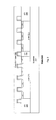
- FIG. 2A is an illustration showing a top view of the wafer portion 200 , in accordance with one embodiment of the present invention.
- FIG. 2B is an illustration showing a vertical cross-section view of the wafer portion 200 , in accordance with one embodiment of the present invention.
- the vertical cross-section view (A-A) of FIG. 2B corresponds to the vertical cross-section of the wafer portion 200 at a location corresponding to bracket A-A in FIG. 2A .
- the wafer portion 200 includes a number of gate structures 205 defined thereon in a parallel orientation with respect to each other.
- FIG. 2C is an illustration showing an expanded view of a given gate structure 205 , in accordance with one embodiment of the present invention. It should be understood that the given gate structure 205 , as shown in FIG. 2C , is representative of the other gate structures 205 within the wafer portion 200 .
- Each gate structure 205 is defined as a linear gate structure having a central conductive region 219 , a top region 217 , and sidewall spacers 215 .
- the central conductive region 219 can be formed of polysilicon, metal, or essentially any other suitable electrically conductive material.
- the top region 217 is formed of an electrically conductive material that is capable of reflecting photons, such a those of incoherent light.
- the top region 217 is formed of NiSi 2 .
- the sidewall spacers 215 can be formed of essentially any suitable material.
- the sidewall spacers 215 are formed of Si 3 N 4 .
- Each gate structure 205 is defined as a linear gate structure having a top surface 222 , substantially parallel side surfaces 220 , a width 216 defined perpendicularly between the side surfaces 220 , and a length 218 extending perpendicular to the width 216 along the top surface 222 .
- each linear gate structure 205 is shown to have a length approximately equal to the length 218 .
- the various gate structures 205 are not required to have the same length.
- any number of the linear gate structures 205 may be segmented to include a number of breaks, depending on the circuit function to be defined.
- Each linear gate structure 205 is devoid of a substantial change in direction along its length.
- a substantial change in direction of a linear gate structure 205 exists when the width 216 of the linear gate structure 205 at any point thereon changes by more than 50% of the nominal width 216 of the linear gate structure 205 along its entire length.
- a substantial change in direction of a linear gate structure 205 exists when the width 216 of the linear gate structure 205 changes from any first location on the linear gate structure 205 to any second location on the linear gate structure 205 by more than 50% of the width 216 at the first location.
- the exemplary wafer portion 200 further includes a number of active areas 203 for NMOS devices, as denoted by (n+), and a number of active areas 201 for PMOS devices, as denoted by (p+).
- the n+ active areas 203 are disposed within a “p well” 211
- the p wells 211 are bordered by shallow trench isolation (STI) regions 209 .
- STI shallow trench isolation
- the wafer portion 200 including the p wells 211 , the STI regions 209 and the gate structures 205 thereabove, is defined over a substrate 213 , such as a silicon substrate. Additionally, the active area regions 201 / 203 between the sidewalls 215 of each gate structure 205 can be defined to have an exposed conductive surface 207 .
- the exposed conductive surface 207 is formed of metal, metal silicide, or a combination thereof.
- a salicide process is performed to form a nickel silicide as the exposed conductive surface 207 present over portions of the active area regions 201 / 203 .
- the wafer portion 200 can include a thin, e.g., 200-300 angstroms thick, etch stop and/or stress liner conformally disposed over its top surface, i.e., conformally disposed over the upper exposed surfaces of the substrate 213 , STI regions 209 , active area regions 201 / 203 , and gate structures 205 .
- etch stop and/or stress liner conformally disposed over its top surface, i.e., conformally disposed over the upper exposed surfaces of the substrate 213 , STI regions 209 , active area regions 201 / 203 , and gate structures 205 .
- the etch stop and/or stress liner is not shown in FIGS. 2A-24B . However, it should be understood that such a conformal layer can be present, if appropriate.
- the wafer portion 200 provided for the SSA contact process has been described in some detail in FIGS. 2A-2C , it should be understood that the SSA contact process is not restricted to the specifically disclosed features of the exemplary wafer portion 200 .
- the SSA contact process described herein can be used to defined contacts on a semiconductor wafer portion that includes either more or less features than what are explicitly disclosed herein with regard to the exemplary wafer portion 200 , so long as the top surface 222 and/or top region 217 of each gate structure is capable of reflecting photons.
- the method proceeds with an operation 117 for depositing a photon absorption layer 301 over the wafer portion 200 .
- the photon absorption layer 301 is formed of amorphous carbon.
- the photon absorption layer 301 can be formed from essentially any material that has a sufficiently strong photon absorption property and has adequate chemical, structural, thermal, and electrical properties as required for successful manufacture and operation of the semiconductor device formed on the wafer portion 200 .
- the sufficiently strong photon absorption property of the photon absorption layer 301 material is evidenced by a minimal backscattering of photons incident upon a surface of the photon absorption layer 301 material.
- FIG. 3 is an illustration showing the photon absorption layer 301 deposited over the wafer portion 200 , in accordance with one embodiment of the present invention.
- the photon absorption layer 301 is initially deposited to fill the regions between the gate structures 205 , and to extend up to a level above the top surfaces 222 of the gate structures 205 .
- An operation 119 is then performed to remove an upper portion of the photon absorption layer 301 so as to expose the top surfaces 222 of the gate structures 205 .
- FIG. 4 is an illustration showing the upper portion of the photon absorption layer 301 removed to expose the top surfaces 222 of the gate structures 205 , in accordance with one embodiment of the present invention.
- the removal of the upper portion of the photon absorption layer 301 in operation 119 can be performed using an etching process, a chemical mechanical planarization (CMP) process, or a combination thereof.
- CMP chemical mechanical planarization
- the photon absorption layer 301 is deposited between the gate structures 205 so as to substantially cover an area of the wafer portion 200 present between the gate structures 205 with the photon absorption layer 301 , while leaving the top surface 222 of each gate structure 205 uncovered.
- the photon absorption layer 301 fills regions adjacent to each gate structure 205 so as to contact the side surfaces 220 of each gate structure 205 without covering the top surface 222 of each gate structure 205 .
- FIG. 5 is an illustration showing the dielectric layer 501 deposited over the wafer portion 200 , in accordance with one embodiment of the present invention.
- the dielectric layer 501 is deposited over both the photon absorption layer 301 and the top surface 222 of each gate structure 205 .
- the dielectric layer 501 is formed of an electrically insulating oxide material.
- the SSA contact fabrication process is not limited to use with a specific type of dielectric layer 501 .
- the dielectric layer 501 can be formed from essentially any material, or stack of materials, having adequate chemical, structural, thermal, and electrical properties as required for successful manufacture and operation of the semiconductor device formed on the wafer portion 200 . Additionally, as part of operation 121 , an upper surface 503 of the deposited dielectric layer 501 is substantially planarized. In one embodiment, planarization of the dielectric layer 501 upper surface 503 is performed using a CMP process. However, in other embodiments, essentially any technique can be used to planarize the dielectric layer 501 , so long as the technique is compatible with the materials present on the wafer portion 200 .
- first hard mask portions 601 A are formed directly over the gate structures 205 .
- first as used herein with regard to the first hard mask portions 601 A, distinguishes a material type used to form the first hard mask portions 601 A.
- second hard mask filaments 1101 A are also used in the SSA fabrication process.
- second as used herein with regard to the second hard mask filaments 1101 A, distinguishes a material type used to form the second hard mask filaments 1101 A, that is different from the “first” material type used to form the first hard mask portions 601 A.
- the first hard mask portions 601 A are formed over a corresponding number of underlying gate structures such that each first hard mask portion 601 A vertically shadows a respective one of the underlying gate structures 205 .
- FIG. 1C is an illustration showing an expanded view of operation 103 , in accordance with one embodiment of the present invention.
- operation 103 includes an operation 123 for depositing a first hard mask layer 601 over the wafer portion 200 . More specifically, the first hard mask layer 601 is deposited over the dielectric layer 501 . An operation 125 is then performed to deposit a negative photoresist layer 603 over the first hard mask layer 601 .
- FIG. 6 is an illustration showing the first hard mask layer 601 deposited over the dielectric layer 501 , and the negative photoresist layer 603 deposited over the first hard mask layer 601 , in accordance with one embodiment of the present invention.
- the first hard mask layer 601 can be defined by essentially any suitable hard mask material.
- the first hard mask layer 601 can be defined as an advanced patterning film (APF) or as a SiON hard mask.
- the first hard mask layer 601 can be deposited on the wafer portion 200 using essentially any hard mask deposition technique.
- the first hard mask layer 601 is deposited using a chemical vapor deposition (CVD) process.
- a negative photoresist material is characterized in that portions of the negative photoresist material that are sufficiently exposed to a light source will made insoluble, i.e., non-removable, in the presence of a developer solution, and underexposed portions of the negative photoresist material will be remain soluble, i.e., removable, in the presence of the developer solution.
- the negative photoresist layer 603 can be defined by essentially any type of negative photoresist material, e.g., photosensitive polymer, so long as the light exposure threshold for cross-linking of the negative photoresist material is suitable for use with a given light source, such that more than a forward exposure of the negative photoresist material to the given light source is required for cross-linking of the negative photoresist material.
- negative photoresist material e.g., photosensitive polymer
- the light exposure threshold of the negative photoresist material is such that a transmission of collimated, incoherent light from the given light source through an upper surface 605 of the negative photoresist layer 603 to a lower surface 607 of the negative photoresist layer 603 , i.e., forward exposure, is not sufficient to cross-link the negative photoresist material.
- the light exposure threshold of the negative photoresist material is such that the forward exposure of the negative photoresist material combined with a reflective exposure of the negative photoresist material, i.e., exposure to light reflected upward from below the lower surface 607 of the negative photoresist layer 603 , is sufficient to cross-link the negative photoresist material.
- the characteristics of the light, e.g., intensity, duration, wavelength, etc., incident upon the negative photoresist layer 603 can be controlled in conjunction with the light exposure threshold of the negative photoresist material such that a specific amount of reflective exposure of the negative photoresist material is required for cross-linking of the negative photoresist material.
- the negative photoresist layer 603 can be deposited on the wafer portion 200 using essentially any photoresist deposition technique, such as spin-on deposition.
- operation 125 for exposing and developing the negative photoresist layer 603 , so as to only leave negative photoresist portions that vertically overlie gate structures 205 .
- operation 125 is performed by uniformly exposing the negative photoresist layer 603 to vertically collimated, incoherent light, whereby the light passes through the negative photoresist layer 603 to be absorbed by the photon absorption layer 301 , and to be reflected by the top surface 222 /top region 217 of the gate structures 205 .
- FIG. 7 is an illustration showing the exposure of the wafer portion 200 to the vertically collimated, incoherent light, in accordance with one embodiment of the present invention.
- both forward and reflected exposures of the negative photoresist layer 603 are required to cross-link the negative photoresist, only those portions of negative photoresist that vertically overlie the reflective top surfaces 222 /top regions 217 of the gate structures will be cross-linked. Also, it should be appreciated that because the light is vertically collimated to be normally, i.e., perpendicularly, incident upon the top surfaces 222 of the gate structures 205 , which are substantially horizontal, only those portions of the negative photoresist layer 603 that are located vertically over the gate structures 205 will be subjected to substantial reflective exposure of the light.
- FIG. 8 is an illustration showing the wafer portion 200 following removal of the non-cross-linked portions of the negative photoresist layer 603 , in accordance with one embodiment of the present invention. As shown in FIG. 8 , exposure and development of the negative photoresist layer 603 in operation 127 leaves the negative photoresist portions 603 A, such that each negative photoresist portion 603 A vertically overlies a respective one of the underlying gate structures 205 .
- operation 129 for removing portions of the first hard mask layer 601 that are not protected by the negative photoresist portions 603 A, thereby forming the first hard mask portions 601 A directly over the gate structures 205 .
- operation 129 is performed using a vertically biased etching process, such that the portions of the first hard mask layer 601 that are not protected by the negative photoresist portions 603 A are removed in a substantially top-down manner.
- FIG. 9 is an illustration showing the wafer portion 200 following removal of the unprotected portions of the first hard mask layer 601 , in accordance with one embodiment of the present invention.
- removal of the unprotected portions of the first hard mask layer 601 in operation 129 leaves the first hard mask portions 601 A, such that each first hard mask portion 601 A vertically shadows a respective one of the underlying gate structures 205 .
- vertical shadowing of a given underlying gate structure 205 by a given first hard mask portion 601 A is defined by the given first hard mask portion 601 A having the substantially same horizontal cross-section size and shape as the given underlying gate structure 205 .
- the horizontal cross-section size and shape refers to the size and shape of the feature, i.e., gate structure 205 or first hard mask portion 601 A, when cut in a horizontal plane substantially parallel to the horizontal surface of the substrate 213 . It should be further appreciated that the horizontal width 901 of each first hard mask portion 601 A is substantially the same as the horizontal width of the top surface 222 /top region 217 of the underlying gate structure 205 .
- FIG. 10 is an illustration showing the wafer portion 200 following removal of the remaining negative photoresist portions 603 A, in accordance with one embodiment of the present invention.
- FIG. 1D is an illustration showing an expanded view of operation 105 , in accordance with one embodiment of the present invention.
- operation 105 includes an operation 133 for conformally depositing a second hard mask layer 1101 over the wafer portion 200 .
- FIG. 11 is an illustration showing the second hard mask layer 1101 conformally deposited over the wafer portion 200 , in accordance with one embodiment of the present invention.
- the second hard mask layer 1101 is conformally deposited over both the dielectric layer 501 and the first hard mask portions 601 A.
- the second hard mask layer 1101 can be defined by essentially any suitable hard mask material, so long as the second hard mask material is different from the first hard mask material used to form the first hard mask portions 601 A. More specifically, the second hard mask material should have an etching selectivity different than that of the first hard mask material, such that the first hard mask material can be etched without substantially etching the second hard mask material.
- the second hard mask layer 1101 can be formed of a nitride material.
- the second hard mask layer 1101 can be deposited on the wafer portion 200 using essentially any hard mask deposition technique. For example, in one embodiment, the second hard mask layer 1101 is conformally deposited using a chemical vapor deposition (CVD) process.
- CVD chemical vapor deposition
- FIG. 12 is an illustration showing the second hard mask filaments 1101 A adjacent to the first hard mask portions 601 A, in accordance with one embodiment of the present invention.
- the second hard mask filaments 1101 A are essentially defined as sidewall spacers adjacent to the first hard mask portions 601 A, such that each side surface of each first hard mask portion 601 A has an adjoining second hard mask filament 1101 A.
- a horizontal width 1201 of each second hard mask filament 1101 A, as measured perpendicular to the sidewall of its adjoining first hard mask portion 601 A, is defined to be substantially the same.
- a vertical cross-section profile of each exposed sidewall 1203 of each second hard mask filament 1101 A is defined to be substantially vertical.
- the vertical cross-section profile of the exposed sidewalls 1203 of the hard mask filaments 1101 A may other than substantially vertical.
- the vertical cross-section profile of the exposed sidewall 1203 of the second hard mask filament 1101 A can be tapered such that the second hard mask filament 1101 A is thicker at its bottom, i.e., at the dielectric layer 501 , relative to its top.
- the second hard mask filaments 1101 A are formed by etching the second hard mask layer 1101 , such that horizontal surfaces of the second hard mask layer 1101 are preferentially etched relative to the vertical surfaces of the second hard mask layer 1101 . It should be understood, however, that other techniques can be utilized to form the second hard mask filaments 1101 A from the second hard mask layer 1101 , such that each second hard mask filament 1101 A is formed as a hard mask spacer extending out from the sidewalls of the first hard mask portions 601 A.
- a combined width of the given first hard mask portion 601 A and its adjoining second hard mask filaments 1101 A is greater than the width of the underlying gate structure 205 .
- a perpendicular spacing 1205 between facing exposed side surfaces of a given pair of neighboring second hard mask filaments 1101 A effectively defines a width of an active area contact to be formed between the given pair of neighboring second hard mask filaments 1101 A. Therefore, because the first hard mask portion 601 A vertically shadows the underlying gate structure 205 , the width 1201 of each second hard mask filament effectively defines an active area contact-to-gate structure 205 spacing.
- FIG. 1E is an illustration showing an expanded view of operation 107 , in accordance with one embodiment of the present invention.
- operation 107 includes an operation 137 for depositing a positive photoresist layer 1301 over the wafer portion 200 .
- FIG. 13 is an illustration showing the positive photoresist layer 1301 deposited over the wafer portion 200 , in accordance with one embodiment of the present invention.
- the positive photoresist layer 1301 is deposited over both the exposed dielectric layer 501 portions, the exposed first hard mask portions 601 A, and the exposed second hard mask filaments 1101 A.
- the positive photoresist layer 1301 can be defined by essentially any type of positive photoresist material.
- the positive photoresist material is characterized in that portions of the positive photoresist material that are sufficiently exposed to a light source will made soluble, i.e., removable, in the presence of a developer solution, and underexposed portions of the positive photoresist material will remain insoluble, i.e., non-removable, in the presence of the developer solution.
- an operation 139 is performed to pattern the positive photoresist layer 1301 with an active area contact mask. More specifically, the positive photoresist layer 1301 is patterned to include a substantially linear opening through the positive photoresist layer 1301 , extending from one first hard mask portion 601 A to a neighboring first hard mask portion 601 A in a direction substantially perpendicular to the length of each of the neighboring first hard mask portions 601 A.
- the patterning of the positive photoresist layer 1301 can be performed using essentially any conventional photolithography technique.
- FIG. 14A is an illustration showing an example active area contact mask used to pattern the positive photoresist layer 1301 , in accordance with one embodiment of the present invention.
- the active area contact mask includes a number of linear openings 1401 .
- Each linear opening 1401 represents an area where the positive photoresist layer 1301 is removed to expose the underlying dielectric layer 501 , first hard mask portions 601 A, and second hard mask filaments 1101 A.
- the linear openings 1401 are shown as “ideal” rectangular-shaped openings, it should be understood that the actual linear openings 1401 may have somewhat rounded ends.
- the rounded ends will lie above the first hard mask portions 601 A and/or the second hard mask filaments 1101 A, but not above the dielectric layer 501 portion that extends perpendicularly between the second hard mask filaments 1101 A.
- FIG. 14B is an illustration showing the vertical cross-section view A-A of the wafer portion 200 with the patterned positive photoresist layer 1301 , in accordance with one embodiment of the present invention.
- Substantially rectangular areas 1403 of the dielectric layer 501 are exposed between the neighboring second hard mask filaments 1101 A within the linear openings 1401 .
- the substantially rectangular areas 1403 of the dielectric layer 501 are bounded on two opposing side by the second hard mask filaments 1101 A, and on the other two opposing sides by the linear opening 1401 of the patterned positive photoresist layer 1301 . It should be appreciated that the substantially rectangular areas 1403 of the dielectric layer 501 represent the horizontal cross-section of the active area contact to be formed.
- the active area contact is to be bounded by the second hard mask filaments 1101 A in the linear openings 1401 , and because the linear openings 1401 are “oversized” with respect to the distance between the sidewalls of the neighboring second hard mask filaments 1101 A, there is some flexibility provided in the indexing of the active area contact mask to the wafer portion 200 when patterning the positive photoresist layer 1301 .
- the linear opening 1401 is offset slightly in its direction of extent between the first hard mask portions 601 A, the substantially rectangular area 1403 of exposed dielectric layer 501 will be unaffected.
- FIG. 15 is an illustration showing the vertical cross-section view A-A of the wafer portion 200 with the passages 1501 etched therein, in accordance with one embodiment of the present invention.
- the passages 1501 for the active area contacts are etched downward through the exposed, substantially rectangular areas 1403 of the dielectric layer 501 within the linear openings 1401 .
- the passages 1501 for the active area contacts are etched in a substantially vertical manner, such that sidewalls of the passages 1501 extend in a substantially vertical manner downward from the periphery of the substantially rectangular areas 1403 of the dielectric layer 501 within the linear openings 1401 .
- the sidewalls of the passages 1501 ideally extend downward in a substantially vertical manner, it should be understood that the sidewalls of the passages 1501 can be slightly tapered.
- the sidewalls of a given passage 1501 can be tapered such that the rectangular opening of the given passage 1501 is slightly smaller at its bottom end relative to its top end.
- a vertically biased etching process can be used to form the passages 1501 for the active area contacts.
- the passages 1501 are etched downward through the underlying portion of the dielectric layer 501 , and the underlying portion of the photon absorption layer 301 to reach the conductive material, e.g., silicide, present at the top of the underlying active area, or to reach an etch stop layer present over the underlying active area.
- the conductive material e.g., silicide
- FIG. 16 is an illustration showing the wafer portion 200 following removal of the patterned photoresist layer 1301 , in accordance with one embodiment of the present invention.
- the patterned photoresist layer 1301 can be removed using essentially any photoresist stripping technique, e.g., chemical stripping, ashing, etc.
- FIG. 1F is an illustration showing an expanded view of operation 109 , in accordance with one embodiment of the present invention.
- operation 109 includes an operation 145 for depositing a positive photoresist layer 1701 over the wafer portion 200 .
- FIG. 17 is an illustration showing the positive photoresist layer 1701 deposited over the wafer portion 200 , in accordance with one embodiment of the present invention. As shown in FIG.
- the positive photoresist layer 1701 is deposited over both the exposed dielectric layer 501 portions, the exposed first hard mask portions 601 A, the exposed second hard mask filaments 1101 A, and within the active area contact passages 1501 previously etched in operation 107 .
- the positive photoresist layer 1701 can be defined by essentially any type of positive photoresist material.
- the positive photoresist material is characterized in that portions of the positive photoresist material that are sufficiently exposed to a light source will made soluble, i.e., removable, in the presence of a developer solution, and underexposed portions of the positive photoresist material will remain insoluble, i.e., non-removable, in the presence of the developer solution.
- an operation 147 is performed to pattern the positive photoresist layer 1701 with a gate contact mask. More specifically, the positive photoresist layer 1701 is patterned to include a number of substantially linear openings through the positive photoresist layer 1701 , each extending across a given first hard mask portion 601 A and across portions of the two second hard mask filaments 1101 A adjacent to the given first hard mask portion 601 A.
- the substantially linear opening defined through the positive photoresist layer 1701 is oriented to extend in a direction substantially perpendicular to the length 218 of the underlying gate structure 205 over which the linear opening is defined.
- the patterning of the positive photoresist layer 1701 can be performed using essentially any conventional photolithography technique.
- FIG. 18A is an illustration showing an example gate contact mask used to pattern the positive photoresist layer 1701 , in accordance with one embodiment of the present invention.
- the gate contact mask includes a number of linear openings 1801 .
- Each linear openings 1801 represents area where the positive photoresist layer 1701 is removed to expose the underlying first hard mask portion 601 A, and adjoining portions of the second hard mask filaments 1101 A.
- the linear openings 1801 are shown as “ideal” rectangular-shaped openings, it should be understood that the actual linear openings 1801 may have somewhat rounded ends. However, it should be noted that the rounded ends of a given linear opening 1801 will lie above the adjoining second hard mask filaments 1101 A, and will not lie above the first hard mask portion 601 A over which the given linear opening 1801 extends.
- FIG. 18B is an illustration showing the vertical cross-section view A-A of the wafer portion 200 with the patterned positive photoresist layer 1701 , in accordance with one embodiment of the present invention.
- Substantially rectangular areas 1803 of first hard mask portions 601 A are exposed between the neighboring second hard mask filaments 1101 A within the linear openings 1801 .
- the substantially rectangular areas 1803 of the first hard mask portions 601 A are bounded on two opposing side by the second hard mask filaments 1101 A, and on the other two opposing sides by the linear opening 1801 of the patterned positive photoresist layer 1701 .
- the substantially rectangular area 1803 of the first hard portion 601 A represents the horizontal cross-section of the gate contact to be formed. Also, it should be appreciated that because the gate contact is to be bounded by the second hard mask filaments 1101 A in the linear opening 1801 , and because the linear opening 1801 is “oversized” with respect to the width of the first hard mask portion 601 A, there is some flexibility provided in the indexing of the gate contact mask to the wafer portion 200 when patterning the positive photoresist layer 1701 . For example, if the linear opening 1801 is offset slightly in its direction of extent between the second hard mask filaments 1101 A, the substantially rectangular area 1803 of the exposed first hard mask portion 601 A will be unaffected.
- FIG. 19 is an illustration showing the vertical cross-section view A-A of the wafer portion 200 with the passages 1901 etched therein, in accordance with one embodiment of the present invention.
- the passages 1901 for the gate contacts are etched downward through the exposed, substantially rectangular areas 1803 of the first hard mask portion 601 A within the linear openings 1801 . It should be appreciated that because the materials of the first hard mask portion 601 A and the second hard mask filament 1101 A are different, these material can be selected to have a substantially different etching selectivity with respect to a given etching process.
- the first hard mask portion 601 A may be defined to etch ten times faster than the second hard mask filaments 1101 A. Therefore, during the particular etching process to be performed in operation 149 , the exposed first hard mask portion 601 A is defined to be preferentially etched without substantially affecting the neighboring exposed second hard mask filaments 1101 A. It should be understood that during the etching of the passages 1901 for the gate contacts, the second hard mask filaments 1101 A are etched very slowly so as to not be substantially removed.
- the passages 1901 for the gate contacts are etched in a substantially vertical manner, such that sidewalls of the passages 1901 extend in a substantially vertical manner downward from the periphery of the substantially rectangular areas 1803 of the exposed first hard mask portion 601 A within the linear openings 1801 .
- the sidewalls of the passages 1901 are not required to extend downward in a substantially vertical manner.
- the sidewalls of the passages 1901 can be slightly tapered, such that the rectangular opening of the given passage 1901 is slightly smaller at its bottom end relative to its top end.
- a vertically biased etching process can be used to form the passages 1901 for the gate contacts.
- the passages 1901 are etched downward through the first hard mask portion 601 A to reach the top surface 222 of the underlying gate structure 205 , or to reach an etch stop layer present over the underlying gate structure 205 .
- FIG. 20 is an illustration showing the wafer portion 200 following removal of the patterned photoresist layer 1701 , in accordance with one embodiment of the present invention.
- the patterned photoresist layer 1701 can be removed using essentially any photoresist stripping technique, e.g., chemical stripping, ashing, etc.
- FIG. 21 is an illustration showing the wafer portion 200 following removal of the first hard mask portions 601 A and the second hard mask filaments 1101 A, in accordance with one embodiment of the present invention.
- Operation 111 can be performed using essentially any hard mask removal technique.
- the first hard mask portions 601 A and the second hard mask filaments 1101 A are removed using a wet stripping technique. It should also be understood that the operation 111 includes removal of any exposed etch stop layer, if present at the bottoms of the passages 1501 and 1901 .
- FIG. 1G is an illustration showing an expanded view of operation 113 , in accordance with one embodiment of the present invention.
- operation 113 includes an operation 153 for depositing a metal layer 2201 over the wafer portion 200 .
- FIG. 22 is an illustration showing the vertical cross-section view A-A of the wafer portion 200 with the metal layer 2201 deposited thereon, in accordance with one embodiment of the present invention.
- the metal layer 2201 is deposited as a liner followed by a metal fill.
- the metal layer 2201 is formed by first depositing a TiN liner over the wafer portion 200 using a chemical vapor deposition (CVD) process or a physical vapor deposition (PVD) process. Then, a tungsten (W) fill layer is deposited over the TiN liner using a CVD process.
- the TiN liner is relatively thin, while the W fill layer completely fills the contact passages 1501 and 1901 .
- an operation 155 is performed to removal excess metal from the top of the wafer portion 200 , so as to leave the top surface of the dielectric layer exposed 501 and the contact passages 1501 and 1901 filled with metal.
- a CMP process can be used to perform operation 155 so as to remove the W fill layer and the TiN liner from the top surface of the dielectric layer 501 .
- FIG. 23 is an illustration showing the vertical cross-section view A-A of the wafer portion 200 with the excess metal layer 2201 removed to leave the active area contacts 2301 and the gate contacts 2303 , in accordance with one embodiment of the present invention.
- fabrication of the wafer portion 200 can continue with fabrication of a metalization layer over the dielectric layer 501 .
- FIG. 24A is an illustration showing a top view of the wafer portion 200 following formation of the active area contacts 2301 and gate contacts 2303 , in accordance with one embodiment of the present invention.
- each active area contact 2301 is substantially centered between its neighboring gate structures 205 .
- each gate contact 2303 is defined to substantially cover the width of the underlying gate structure 205 without extending substantially beyond either of the side surfaces of the underlying gate structure 205 .
- the active area contacts 2301 and the gate contacts 2303 are considered to be super-self-aligned (SSA) contacts with respect to the gate structures 205 .
- SSA super-self-aligned
- FIG. 24B is an illustration showing an expanded view of an area 2401 , as called out in FIG. 24A , in accordance with one embodiment of the present invention.
- the active area contact 2301 is substantially centered between its neighboring gate structures 205 , such that a substantially equal gate-to-active area contact spacing (SGC) exists on each side the active area contact 2301 .
- the gate-to-active area contact spacing (SGC) is defined by the width of the second hard mask filament 1101 A, as measured in the horizontal direction perpendicular to the length 218 of the gate structure 205 .
- the gate pitch (PGA) is equal to the sum of the gate width (WGA), the active area contact width (WCT), and twice the gate-to-active area contact spacing (SGC).
Abstract
Description
Claims (20)
Priority Applications (4)
| Application Number | Priority Date | Filing Date | Title |
|---|---|---|---|
| US14/566,249 US9281371B2 (en) | 2007-12-13 | 2014-12-10 | Super-self-aligned contacts and method for making the same |
| US15/064,323 US9818747B2 (en) | 2007-12-13 | 2016-03-08 | Super-self-aligned contacts and method for making the same |
| US15/811,538 US10461081B2 (en) | 2007-12-13 | 2017-11-13 | Super-self-aligned contacts and method for making the same |
| US16/667,750 US20200066722A1 (en) | 2007-12-13 | 2019-10-29 | Super-Self-Aligned Contacts and Method for Making the Same |
Applications Claiming Priority (3)
| Application Number | Priority Date | Filing Date | Title |
|---|---|---|---|
| US11/956,305 US8541879B2 (en) | 2007-12-13 | 2007-12-13 | Super-self-aligned contacts and method for making the same |
| US14/033,952 US8951916B2 (en) | 2007-12-13 | 2013-09-23 | Super-self-aligned contacts and method for making the same |
| US14/566,249 US9281371B2 (en) | 2007-12-13 | 2014-12-10 | Super-self-aligned contacts and method for making the same |
Related Parent Applications (1)
| Application Number | Title | Priority Date | Filing Date |
|---|---|---|---|
| US14/033,952 Continuation US8951916B2 (en) | 2007-12-13 | 2013-09-23 | Super-self-aligned contacts and method for making the same |
Related Child Applications (1)
| Application Number | Title | Priority Date | Filing Date |
|---|---|---|---|
| US15/064,323 Continuation US9818747B2 (en) | 2007-12-13 | 2016-03-08 | Super-self-aligned contacts and method for making the same |
Publications (2)
| Publication Number | Publication Date |
|---|---|
| US20150091190A1 US20150091190A1 (en) | 2015-04-02 |
| US9281371B2 true US9281371B2 (en) | 2016-03-08 |
Family
ID=40752138
Family Applications (6)
| Application Number | Title | Priority Date | Filing Date |
|---|---|---|---|
| US11/956,305 Expired - Fee Related US8541879B2 (en) | 2006-03-09 | 2007-12-13 | Super-self-aligned contacts and method for making the same |
| US14/033,952 Expired - Fee Related US8951916B2 (en) | 2007-12-13 | 2013-09-23 | Super-self-aligned contacts and method for making the same |
| US14/566,249 Expired - Fee Related US9281371B2 (en) | 2007-12-13 | 2014-12-10 | Super-self-aligned contacts and method for making the same |
| US15/064,323 Expired - Fee Related US9818747B2 (en) | 2007-12-13 | 2016-03-08 | Super-self-aligned contacts and method for making the same |
| US15/811,538 Expired - Fee Related US10461081B2 (en) | 2007-12-13 | 2017-11-13 | Super-self-aligned contacts and method for making the same |
| US16/667,750 Abandoned US20200066722A1 (en) | 2007-12-13 | 2019-10-29 | Super-Self-Aligned Contacts and Method for Making the Same |
Family Applications Before (2)
| Application Number | Title | Priority Date | Filing Date |
|---|---|---|---|
| US11/956,305 Expired - Fee Related US8541879B2 (en) | 2006-03-09 | 2007-12-13 | Super-self-aligned contacts and method for making the same |
| US14/033,952 Expired - Fee Related US8951916B2 (en) | 2007-12-13 | 2013-09-23 | Super-self-aligned contacts and method for making the same |
Family Applications After (3)
| Application Number | Title | Priority Date | Filing Date |
|---|---|---|---|
| US15/064,323 Expired - Fee Related US9818747B2 (en) | 2007-12-13 | 2016-03-08 | Super-self-aligned contacts and method for making the same |
| US15/811,538 Expired - Fee Related US10461081B2 (en) | 2007-12-13 | 2017-11-13 | Super-self-aligned contacts and method for making the same |
| US16/667,750 Abandoned US20200066722A1 (en) | 2007-12-13 | 2019-10-29 | Super-Self-Aligned Contacts and Method for Making the Same |
Country Status (3)
| Country | Link |
|---|---|
| US (6) | US8541879B2 (en) |
| TW (1) | TWI381447B (en) |
| WO (1) | WO2009076661A2 (en) |
Cited By (2)
| Publication number | Priority date | Publication date | Assignee | Title |
|---|---|---|---|---|
| US10216890B2 (en) | 2004-04-21 | 2019-02-26 | Iym Technologies Llc | Integrated circuits having in-situ constraints |
| US10395990B2 (en) | 2016-11-14 | 2019-08-27 | Samsung Electronics Co., Ltd. | Semiconductor device and method for fabricating the same |
Families Citing this family (14)
| Publication number | Priority date | Publication date | Assignee | Title |
|---|---|---|---|---|
| US8890256B2 (en) * | 2009-03-20 | 2014-11-18 | International Business Machines Corporation | Structure for heavy ion tolerant device, method of manufacturing the same and structure thereof |
| US8541311B2 (en) * | 2010-12-22 | 2013-09-24 | GlobalFoundries, Inc. | Integrated circuit fabrication methods utilizing embedded hardmask layers for high resolution patterning |
| US9337318B2 (en) | 2012-10-26 | 2016-05-10 | Taiwan Semiconductor Manufacturing Company, Ltd. | FinFET with dummy gate on non-recessed shallow trench isolation (STI) |
| US9087587B2 (en) * | 2013-03-15 | 2015-07-21 | GlobalFoundries, Inc. | Integrated circuits and methods for operating integrated circuits with non-volatile memory |
| US9312174B2 (en) | 2013-12-17 | 2016-04-12 | United Microelectronics Corp. | Method for manufacturing contact plugs for semiconductor devices |
| KR102150942B1 (en) * | 2014-12-01 | 2020-09-03 | 삼성전자주식회사 | Semiconductor device including fin FET |
| US20200402971A1 (en) * | 2015-01-16 | 2020-12-24 | Taiwan Semiconductor Manufacturing Company, Ltd. | Methods of manufacturing semiconductor devices |
| US9806070B2 (en) * | 2015-01-16 | 2017-10-31 | Taiwan Semiconductor Manufacturing Company, Ltd. | Semiconductor device layout, memory device layout, and method of manufacturing semiconductor device |
| US9985122B2 (en) * | 2015-05-19 | 2018-05-29 | Taiwan Semiconductor Manufacturing Company Ltd. | Semiconductor structures |
| US10043905B2 (en) * | 2015-09-11 | 2018-08-07 | Toshiba Memory Corporation | Semiconductor device |
| CN106611711B (en) * | 2015-10-22 | 2019-09-27 | 中芯国际集成电路制造(北京)有限公司 | The forming method of semiconductor devices |
| KR102532169B1 (en) * | 2015-12-22 | 2023-05-16 | 인텔 코포레이션 | Pin-based III-V/SI or GE CMOS SAGE integration |
| US11011417B2 (en) | 2019-05-31 | 2021-05-18 | International Business Machines Corporation | Method and structure of metal cut |
| CN112736079A (en) | 2019-10-28 | 2021-04-30 | 联华电子股份有限公司 | Semiconductor device having contact plug connected to gate structure of PMOS region |
Citations (628)
| Publication number | Priority date | Publication date | Assignee | Title |
|---|---|---|---|---|
| US4197555A (en) | 1975-12-29 | 1980-04-08 | Fujitsu Limited | Semiconductor device |
| US4417161A (en) | 1980-09-04 | 1983-11-22 | Matsushita Electric Industrial Co., Ltd. | Complementary channel type MOS transistor exclusive OR/NOR logic gate circuit |
| JPS58182242U (en) | 1982-05-28 | 1983-12-05 | パイオニア株式会社 | Push button with slide lock |
| US4424460A (en) | 1981-07-14 | 1984-01-03 | Rockwell International Corporation | Apparatus and method for providing a logical exclusive OR/exclusive NOR function |
| US4613940A (en) | 1982-11-09 | 1986-09-23 | International Microelectronic Products | Method and structure for use in designing and building electronic systems in integrated circuits |
| JPS61182244U (en) | 1985-05-02 | 1986-11-13 | ||
| US4657628A (en) | 1985-05-01 | 1987-04-14 | Texas Instruments Incorporated | Process for patterning local interconnects |
| US4682202A (en) | 1983-07-29 | 1987-07-21 | Fujitsu Limited | Master slice IC device |
| US4745084A (en) | 1986-11-12 | 1988-05-17 | Vlsi Technology, Inc. | Method of making a customized semiconductor integrated device |
| US4780753A (en) | 1982-03-03 | 1988-10-25 | Mitsubishi Denki Kabushiki Kaisha | Semiconductor integrated circuit device |
| JPS63310136A (en) | 1987-06-12 | 1988-12-19 | Nippon Telegr & Teleph Corp <Ntt> | Complementary mis master slice logic integrated circuit |
| US4801986A (en) | 1987-04-03 | 1989-01-31 | General Electric Company | Vertical double diffused metal oxide semiconductor VDMOS device with increased safe operating area and method |
| US4804636A (en) | 1985-05-01 | 1989-02-14 | Texas Instruments Incorporated | Process for making integrated circuits having titanium nitride triple interconnect |
| US4812688A (en) | 1987-12-30 | 1989-03-14 | International Business Machines Corporation | Transistor delay circuits |
| EP0102644B1 (en) | 1982-09-06 | 1989-07-19 | Hitachi, Ltd. | Semiconductor integrated circuit device |
| JPH01284115A (en) | 1988-05-11 | 1989-11-15 | Sharp Corp | Logical circuit |
| US4884115A (en) | 1987-02-27 | 1989-11-28 | Siemens Aktiengesellschaft | Basic cell for a gate array arrangement in CMOS Technology |
| US4928160A (en) | 1989-01-17 | 1990-05-22 | Ncr Corporation | Gate isolated base cell structure with off-grid gate polysilicon pattern |
| US4975756A (en) | 1985-05-01 | 1990-12-04 | Texas Instruments Incorporated | SRAM with local interconnect |
| JPH03165061A (en) | 1989-11-22 | 1991-07-17 | Hitachi Ltd | Semiconductor integrated circuit device |
| US5068603A (en) | 1987-10-07 | 1991-11-26 | Xilinx, Inc. | Structure and method for producing mask-programmed integrated circuits which are pin compatible substitutes for memory-configured logic arrays |
| US5079614A (en) | 1990-09-26 | 1992-01-07 | S-Mos Systems, Inc. | Gate array architecture with basic cell interleaved gate electrodes |
| US5097422A (en) | 1986-10-10 | 1992-03-17 | Cascade Design Automation Corporation | Method and apparatus for designing integrated circuits |
| US5117277A (en) | 1989-01-27 | 1992-05-26 | Hitachi, Ltd. | Semiconductor integrated circuit device with improved connection pattern of signal wirings |
| US5121186A (en) | 1984-06-15 | 1992-06-09 | Hewlett-Packard Company | Integrated circuit device having improved junction connections |
| US5208765A (en) | 1990-07-20 | 1993-05-04 | Advanced Micro Devices, Inc. | Computer-based method and system for product development |
| JPH05152937A (en) | 1991-11-26 | 1993-06-18 | Hitachi Ltd | Logic gate circuit |
| US5224057A (en) | 1989-02-28 | 1993-06-29 | Kabushiki Kaisha Toshiba | Arrangement method for logic cells in semiconductor IC device |
| JPH05211437A (en) | 1992-01-20 | 1993-08-20 | Nec Corp | Logic circuit |
| JPH05218362A (en) | 1992-02-04 | 1993-08-27 | Sharp Corp | Basic cells of gate array |
| US5242770A (en) | 1992-01-16 | 1993-09-07 | Microunity Systems Engineering, Inc. | Mask for photolithography |
| US5268319A (en) | 1988-06-08 | 1993-12-07 | Eliyahou Harari | Highly compact EPROM and flash EEPROM devices |
| US5298774A (en) | 1990-01-11 | 1994-03-29 | Mitsubishi Denki Kabushiki Kaisha | Gate array system semiconductor integrated circuit device |
| US5313426A (en) | 1991-12-09 | 1994-05-17 | Oki Electric Industry Co., Ltd. | Semiconductor memory device |
| US5351197A (en) | 1989-04-13 | 1994-09-27 | Cascade Design Automation Corporation | Method and apparatus for designing the layout of a subcircuit in an integrated circuit |
| US5359226A (en) | 1993-02-02 | 1994-10-25 | Paradigm Technology, Inc. | Static memory with self aligned contacts and split word lines |
| US5365454A (en) | 1990-10-18 | 1994-11-15 | Mitsubishi Denki Kabushiki Kaisha | Layout designing method for a semiconductor integrated circuit device |
| US5367187A (en) | 1992-12-22 | 1994-11-22 | Quality Semiconductor, Inc. | Master slice gate array integrated circuits with basic cells adaptable for both input/output and logic functions |
| US5378649A (en) | 1994-04-08 | 1995-01-03 | United Microelectronics Corporation | Process for producing non-volatile memory devices having closely spaced buried bit lines and non-overlapping code implant areas |
| US5396128A (en) | 1993-09-13 | 1995-03-07 | Motorola, Inc. | Output circuit for interfacing integrated circuits having different power supply potentials |
| US5420447A (en) | 1993-01-29 | 1995-05-30 | Sgs-Thomson Microelectronics, Inc. | Double buffer base gate array cell |
| JPH07153927A (en) | 1993-12-01 | 1995-06-16 | Nec Corp | Semiconductor integrated circuit |
| US5461577A (en) | 1987-08-04 | 1995-10-24 | Texas Instruments Incorporated | Comprehensive logic circuit layout system |
| JPH07302706A (en) | 1994-05-02 | 1995-11-14 | Tokin Corp | Magnetic garnet oxide powder and its manufacture |
| US5471403A (en) | 1991-03-08 | 1995-11-28 | Mitsubishi Denki Kabushiki Kaisha | Method for predicting the three-dimensional topography of surfaces of semiconductor devices after reflow processing |
| US5497334A (en) | 1993-02-19 | 1996-03-05 | International Business Machines Corporation | Application generator for use in verifying a hierarchical circuit design |
| US5497337A (en) | 1994-10-21 | 1996-03-05 | International Business Machines Corporation | Method for designing high-Q inductors in silicon technology without expensive metalization |
| US5526307A (en) | 1992-01-22 | 1996-06-11 | Macronix International Co., Ltd. | Flash EPROM integrated circuit architecture |
| US5536955A (en) | 1993-03-29 | 1996-07-16 | Toppan Electronics (Usa) Inc. | Electronic devices for use in generating integrated circuit structures and method therefor |
| US5545904A (en) | 1986-01-17 | 1996-08-13 | Quick Technologies Ltd. | Personalizable gate array devices |
| US5581202A (en) | 1993-11-08 | 1996-12-03 | Hitachi, Ltd. | Semiconductor integrated circuit device and production method thereof |
| US5581098A (en) | 1995-05-05 | 1996-12-03 | Circuit Integration Technology, Inc. | Circuit routing structure using fewer variable masks |
| US5612893A (en) | 1993-12-22 | 1997-03-18 | Vlsi Technology, Inc. | Method and apparatus for compacting integrataed circuits with transistor sizing |
| US5636002A (en) | 1994-04-29 | 1997-06-03 | Lucent Technologies Inc. | Auxiliary mask features for enhancing the resolution of photolithography |
| EP0788166A2 (en) | 1996-01-31 | 1997-08-06 | International Business Machines Corporation | Integrated circuit chip having gate array book personalisation using local interconnect |
| US5656861A (en) | 1990-01-12 | 1997-08-12 | Paradigm Technology, Inc. | Self-aligning contact and interconnect structure |
| US5682323A (en) | 1995-03-06 | 1997-10-28 | Lsi Logic Corporation | System and method for performing optical proximity correction on macrocell libraries |
| US5684733A (en) | 1996-09-30 | 1997-11-04 | Holtek Microelectronics, Inc. | Fixed resistance high density parallel ROM device |
| US5684311A (en) | 1994-05-10 | 1997-11-04 | Texas Instruments Incorporated | Base cell for BiCMOS and CMOS gate arrays |
| JP2684980B2 (en) | 1993-12-24 | 1997-12-03 | 日本電気株式会社 | Semiconductor memory device and manufacturing method thereof |
| US5698873A (en) | 1996-03-08 | 1997-12-16 | Lsi Logic Corporation | High density gate array base cell architecture |
| US5705301A (en) | 1996-02-27 | 1998-01-06 | Lsi Logic Corporation | Performing optical proximity correction with the aid of design rule checkers |
| US5723883A (en) | 1995-11-14 | 1998-03-03 | In-Chip | Gate array cell architecture and routing scheme |
| US5723908A (en) | 1993-03-11 | 1998-03-03 | Kabushiki Kaisha Toshiba | Multilayer wiring structure |
| US5740068A (en) | 1996-05-30 | 1998-04-14 | International Business Machines Corporation | Fidelity enhancement of lithographic and reactive-ion-etched images by optical proximity correction |
| US5745374A (en) | 1994-07-22 | 1998-04-28 | Kabushiki Kaisha Toshiba | Layout method for semiconductor integrated circuit and layout apparatus for semiconductor integrated circuit |
| JPH10116911A (en) | 1996-10-09 | 1998-05-06 | Toshiba Corp | Re-layout method for semiconductor integrated circuit and medium on which re-layout program for semiconductor integrated circuit is recorded |
| US5764533A (en) | 1995-08-01 | 1998-06-09 | Sun Microsystems, Inc. | Apparatus and methods for generating cell layouts |
| US5774367A (en) | 1995-07-24 | 1998-06-30 | Motorola, Inc. | Method of selecting device threshold voltages for high speed and low power |
| US5780909A (en) | 1995-02-28 | 1998-07-14 | Nec Corporation | Semiconductor memory device with a two-layer top gate |
| US5789776A (en) | 1995-09-22 | 1998-08-04 | Nvx Corporation | Single poly memory cell and array |
| US5790417A (en) | 1996-09-25 | 1998-08-04 | Taiwan Semiconductor Manufacturing Company Ltd. | Method of automatic dummy layout generation |
| US5796624A (en) | 1994-09-16 | 1998-08-18 | Research Foundation Of State University Of New York | Method and apparatus for designing circuits for wave pipelining |
| US5796128A (en) | 1996-07-25 | 1998-08-18 | Translogic Technology, Inc. | Gate array with fully wired multiplexer circuits |
| US5798298A (en) | 1996-02-09 | 1998-08-25 | United Microelectronics Corporation | Method of automatically generating dummy metals for multilevel interconnection |
| US5814844A (en) | 1995-09-28 | 1998-09-29 | Nippondenso Co., Ltd. | Gate array having highly flexible interconnection structure |
| US5825203A (en) | 1995-11-28 | 1998-10-20 | Hitachi, Ltd. | Variable logic integrated circuit device having connections through switch matrix and top layers for inter-cell connections |
| US5834851A (en) | 1990-02-09 | 1998-11-10 | Hitachi, Ltd. | SRAM having load transistor formed above driver transistor |
| US5838594A (en) | 1995-02-24 | 1998-11-17 | Fujitsu Limited | Method and apparatus for generating finite element meshes, and analyzing method and apparatus |
| US5841663A (en) | 1995-09-14 | 1998-11-24 | Vlsi Technology, Inc. | Apparatus and method for synthesizing integrated circuits using parameterized HDL modules |
| KR19980084215A (en) | 1997-05-22 | 1998-12-05 | 김영환 | Method of manufacturing transistor of semiconductor device |
| US5847421A (en) | 1996-07-15 | 1998-12-08 | Kabushiki Kaisha Toshiba | Logic cell having efficient optical proximity effect correction |
| US5852562A (en) | 1994-12-13 | 1998-12-22 | Matsushita Electric Industrial Co., Ltd. | Method and apparatus for designing an LSI layout utilizing cells having a predetermined wiring height in order to reduce wiring zones |
| US5858580A (en) | 1997-09-17 | 1999-01-12 | Numerical Technologies, Inc. | Phase shifting circuit manufacture method and apparatus |
| JPH1145948A (en) | 1997-05-30 | 1999-02-16 | St Microelectron Inc | Layout for sram structure |
| US5900340A (en) | 1997-03-03 | 1999-05-04 | Motorola, Inc. | One dimensional lithographic proximity correction using DRC shape functions |
| US5905287A (en) | 1996-04-25 | 1999-05-18 | Nec Corporation | Semiconductor device with high voltage protection |
| US5908827A (en) | 1992-12-22 | 1999-06-01 | Applied Research Systems Ars Holding N.V. | Protein from urine named component B |
| US5915199A (en) | 1998-06-04 | 1999-06-22 | Sharp Microelectronics Technology, Inc. | Method for manufacturing a CMOS self-aligned strapped interconnection |
| US5917207A (en) | 1993-07-01 | 1999-06-29 | Lsi Logic Corporation | Programmable polysilicon gate array base cell architecture |
| US5920486A (en) | 1996-08-16 | 1999-07-06 | International Business Machines Corporation | Parameterized cells for generating dense layouts of VLSI circuits |
| US5923060A (en) | 1996-09-27 | 1999-07-13 | In-Chip Systems, Inc. | Reduced area gate array cell design based on shifted placement of alternate rows of cells |
| KR19990057943A (en) | 1997-12-30 | 1999-07-15 | 김영환 | Contact hole formation method of semiconductor device |
| US5929469A (en) | 1996-12-25 | 1999-07-27 | Kabushiki Kaisha Toshiba | Contact holes of a different pitch in an application specific integrated circuit |
| US5930163A (en) | 1996-12-19 | 1999-07-27 | Kabushiki Kaisha Toshiba | Semiconductor memory device having two P-well layout structure |
| US5935763A (en) | 1996-06-11 | 1999-08-10 | International Business Machines Corporation | Self-aligned pattern over a reflective layer |
| US5949101A (en) | 1994-08-31 | 1999-09-07 | Kabushiki Kaisha Toshiba | Semiconductor memory device comprising multi-level logic value of the threshold voltage |
| US5973507A (en) | 1995-06-13 | 1999-10-26 | Fujitsu Limited | Exclusive-or gate for use in delay using transmission gate circuitry |
| US5977574A (en) | 1997-03-28 | 1999-11-02 | Lsi Logic Corporation | High density gate array cell architecture with sharing of well taps between cells |
| US5977305A (en) | 1990-04-20 | 1999-11-02 | Cold Spring Harbor Laboratories | Cloning by complementation and related processes |
| US5998879A (en) | 1997-02-03 | 1999-12-07 | Nec Corporation | Semiconductor memory device |
| US6009251A (en) | 1997-09-30 | 1999-12-28 | Synopsys, Inc. | Method and system for layout verification of an integrated circuit design with reusable subdesigns |
| US6026223A (en) | 1996-06-28 | 2000-02-15 | Scepanovic; Ranko | Advanced modular cell placement system with overlap remover with minimal noise |
| US6037617A (en) | 1997-02-03 | 2000-03-14 | Nec Corporation | SOI IGFETs having raised integration level |
| US6037613A (en) | 1997-02-24 | 2000-03-14 | Sharp Kabushiki Kaisha | Bidirectional thyristor device |
| US6044007A (en) | 1999-03-24 | 2000-03-28 | Advanced Micro Devices, Inc. | Modification of mask layout data to improve writeability of OPC |
| TW386288B (en) | 1997-04-14 | 2000-04-01 | Ibm | New structure for low cost mixed memory integration, new nvram structure, and process for forming the mixed memory and nvram structures |
| US6054872A (en) | 1996-12-27 | 2000-04-25 | Kabushiki Kaisha Toshiba | Semiconductor integrated circuit with mixed gate array and standard cell |
| US6063132A (en) | 1998-06-26 | 2000-05-16 | International Business Machines Corporation | Method for verifying design rule checking software |
| KR20000028830A (en) | 1998-10-05 | 2000-05-25 | 니시무로 타이죠 | A semiconductor device and a method of making thereof |
| US6077310A (en) | 1995-12-22 | 2000-06-20 | Kabushiki Kaisha Toshiba | Optical proximity correction system |
| US6080206A (en) | 1996-12-27 | 2000-06-27 | Oki Electric Industry Co., Ltd. | Method of laying out interconnections |
| US6084437A (en) | 1995-09-22 | 2000-07-04 | Kawasaki Steel Corporation | Logic circuit utilizing pass transistors and logic gate |
| US6091845A (en) | 1998-02-24 | 2000-07-18 | Micron Technology, Inc. | Inspection technique of photomask |
| US6100025A (en) | 1990-04-20 | 2000-08-08 | Cold Spring Harbor Laboratory | Cloning by complementation and related processes |
| US6099584A (en) | 1996-12-06 | 2000-08-08 | Vsli Technology, Inc. | System to fix post-layout timing and design rules violations |
| US6114071A (en) | 1997-11-24 | 2000-09-05 | Asml Masktools Netherlands B.V. | Method of fine feature edge tuning with optically-halftoned mask |
| US6144227A (en) | 1997-04-18 | 2000-11-07 | Sharp Kabushiki Kaisha | MOS logic circuit and semiconductor apparatus including the same |
| US6159839A (en) | 1999-02-11 | 2000-12-12 | Vanguard International Semiconductor Corporation | Method for fabricating borderless and self-aligned polysilicon and metal contact landing plugs for multilevel interconnections |
| US6166415A (en) | 1998-11-02 | 2000-12-26 | Mitsubishi Denki Kabushiki Kaisha | Semiconductor device with improved noise resistivity |
| US6166560A (en) | 1996-09-09 | 2000-12-26 | Sanyo Electric Co., Ltd. | Basic cell structure having a plurality of transistors for master slice type semiconductor integrated circuit device |
| US6174742B1 (en) | 1998-10-30 | 2001-01-16 | Lsi Logic Corporation | Off-grid metal layer utilization |
| US6182272B1 (en) | 1998-07-16 | 2001-01-30 | Lsi Logic Corporation | Metal layer assignment |
| US6194912B1 (en) | 1999-03-11 | 2001-02-27 | Easic Corporation | Integrated circuit device |
| US6194104B1 (en) | 1999-10-12 | 2001-02-27 | Taiwan Semiconductor Manufacturing Company | Optical proximity correction (OPC) method for improving lithography process window |
| JP2001056463A (en) | 1999-08-20 | 2001-02-27 | Casio Comput Co Ltd | Liquid crystal display device |
| JP2001068558A (en) | 1999-08-30 | 2001-03-16 | Hitachi Ltd | Semiconductor integrated circuit device |
| US6209123B1 (en) | 1996-11-01 | 2001-03-27 | Motorola, Inc. | Methods of placing transistors in a circuit layout and semiconductor device with automatically placed transistors |
| US6230299B1 (en) | 1998-03-31 | 2001-05-08 | Mentor Graphics Corporation | Method and apparatus for extracting and storing connectivity and geometrical data for a deep sub-micron integrated circuit design |
| US6240542B1 (en) | 1998-07-14 | 2001-05-29 | Lsi Logic Corporation | Poly routing for chip interconnects with minimal impact on chip performance |
| US6249902B1 (en) | 1998-01-09 | 2001-06-19 | Silicon Perspective Corporation | Design hierarchy-based placement |
| JP2001168707A (en) | 1999-12-03 | 2001-06-22 | Sony Corp | Logic circuit and full adder using the same |
| US6255600B1 (en) | 1993-03-01 | 2001-07-03 | The Board Of Trustees Of The University Of Arkansas | Electronic interconnection medium having offset electrical mesh plane |
| US6255845B1 (en) | 1999-11-16 | 2001-07-03 | Advanced Micro Devices, Inc. | Efficient use of spare gates for post-silicon debug and enhancements |
| US6262487B1 (en) | 1998-06-23 | 2001-07-17 | Kabushiki Kaisha Toshiba | Semiconductor integrated circuit device, semiconductor integrated circuit wiring method, and cell arranging method |
| US6269472B1 (en) | 1996-02-27 | 2001-07-31 | Lsi Logic Corporation | Optical proximity correction method and apparatus |
| US6275973B1 (en) | 1998-10-30 | 2001-08-14 | Lsi Logic Corporation | Integrated circuit design with delayed cell selection |
| US6282696B1 (en) | 1997-08-15 | 2001-08-28 | Lsi Logic Corporation | Performing optical proximity correction with the aid of design rule checkers |
| US6291276B1 (en) | 1995-11-20 | 2001-09-18 | Micron Technology, Inc. | Cross coupled thin film transistors and static random access memory cell |
| US6297668B1 (en) | 1998-11-25 | 2001-10-02 | Manopower Technologies, Inc. | Serial device compaction for improving integrated circuit layouts |
| US6297674B1 (en) | 1998-11-10 | 2001-10-02 | Hitachi, Ltd. | Semiconductor integrated circuit for low power and high speed operation |
| JP2001272228A (en) | 2000-03-24 | 2001-10-05 | Railway Technical Res Inst | System and method for measuring amount of relative displacement |
| US6303252B1 (en) | 1999-12-27 | 2001-10-16 | United Microelectronics Corp. | Reticle having assist feature between semi-dense lines |
| US20010049813A1 (en) | 1998-06-29 | 2001-12-06 | Chun Chan | Integrated circuit incorporating a power mesh |
| US6331791B1 (en) | 1999-10-06 | 2001-12-18 | Industrial Technology Research Institute | Charge-redistribution low-swing differential logic circuit |
| US6331733B1 (en) | 1999-08-10 | 2001-12-18 | Easic Corporation | Semiconductor device |
| US20020003270A1 (en) | 2000-07-10 | 2002-01-10 | Mitsubishi Denki Kabushiki Kaisha | Semiconductor device |
| JP2002026296A (en) | 2000-06-22 | 2002-01-25 | Internatl Business Mach Corp <Ibm> | Semiconductor integrated circuit device |
| US20020015899A1 (en) | 2000-05-01 | 2002-02-07 | Chen Jang Fung | Hybrid phase-shift mask |
| US6347062B2 (en) | 2000-05-16 | 2002-02-12 | Mitsubishi Denki Kabushiki Kaisha | Semiconductor memory device |
| US6356112B1 (en) | 2000-03-28 | 2002-03-12 | Translogic Technology, Inc. | Exclusive or/nor circuit |
| US6359804B2 (en) | 1998-04-16 | 2002-03-19 | Mitsubishi Denki Kabushiki Kaisha | Static semiconductor memory cell formed in an n-well and p-well |
| US6370679B1 (en) | 1997-09-17 | 2002-04-09 | Numerical Technologies, Inc. | Data hierarchy layout correction and verification method and apparatus |
| US6378110B1 (en) | 1998-03-31 | 2002-04-23 | Synopsys, Inc. | Layer-based rule checking for an integrated circuit layout |
| US6380592B2 (en) | 1997-11-28 | 2002-04-30 | Stmicroelectronics S.R.L. | Low power RAM memory cell using a precharge line pulse during write operation |
| KR20020034313A (en) | 2000-10-31 | 2002-05-09 | 박종섭 | Method of manufacturing sram cell |
| US6393601B1 (en) | 1997-04-14 | 2002-05-21 | Matsushita Electric Industrial Co., Ltd. | Layout designing apparatus for integrated circuit, transistor size determining apparatus, circuit characteristic evaluating method, and transistor size determining method |
| US6399972B1 (en) | 2000-03-13 | 2002-06-04 | Oki Electric Industry Co., Ltd. | Cell based integrated circuit and unit cell architecture therefor |
| US6400183B2 (en) | 1997-11-28 | 2002-06-04 | Hitachi, Ltd. | Logic circuit and its forming method |
| US20020068423A1 (en) | 2000-10-04 | 2002-06-06 | Park Young-Hoon | Contact forming method for semiconductor device |
| US6408427B1 (en) | 2000-02-22 | 2002-06-18 | The Regents Of The University Of California | Wire width planning and performance optimization for VLSI interconnects |
| US20020079927A1 (en) | 1997-12-26 | 2002-06-27 | Hitachi Ltd. | Semiconductor integrated circuit device, storage medium on which cell library is stored and designing method for semiconductor integrated circuit |
| JP2002184870A (en) | 2000-12-18 | 2002-06-28 | Mitsubishi Electric Corp | Static semiconductor storage device |
| US6415421B2 (en) | 2000-06-13 | 2002-07-02 | Mentor Graphics Corporation | Integrated verification and manufacturability tool |
| US6416907B1 (en) | 2000-04-27 | 2002-07-09 | Micron Technology, Inc. | Method for designing photolithographic reticle layout, reticle, and photolithographic process |
| US6417549B1 (en) | 2000-01-12 | 2002-07-09 | Samsung Electronics Co., Ltd. | Static random access memory device and method for manufacturing the same |
| US6421820B1 (en) | 1999-12-13 | 2002-07-16 | Infineon Technologies Ag | Semiconductor device fabrication using a photomask with assist features |
| US6425112B1 (en) | 1999-06-17 | 2002-07-23 | International Business Machines Corporation | Auto correction of error checked simulated printed images |
| US6426269B1 (en) | 1999-10-21 | 2002-07-30 | International Business Machines Corporation | Dummy feature reduction using optical proximity effect correction |
| US6436805B1 (en) | 1999-09-01 | 2002-08-20 | Micron Technology, Inc. | Local interconnect structures and methods for making the same |
| US6445049B1 (en) | 1997-06-30 | 2002-09-03 | Artisan Components, Inc. | Cell based array comprising logic, transfer and drive cells |
| US6445065B1 (en) | 2000-06-06 | 2002-09-03 | In-Chip Systems, Inc. | Routing driven, metal programmable integrated circuit architecture with multiple types of core cells |
| JP2002258463A (en) | 2001-03-05 | 2002-09-11 | Dainippon Printing Co Ltd | Photomask pattern defect inspecting method and detecting method for fine figure pattern |
| KR20020070777A (en) | 2001-03-01 | 2002-09-11 | 가부시키가이샤 히타치세이사쿠쇼 | A semiconductor device |
| JP2002289703A (en) | 2001-01-22 | 2002-10-04 | Nec Corp | Semiconductor memory and its manufacturing method |
| US6467072B1 (en) | 1998-11-20 | 2002-10-15 | Via Technologies, Inc. | Method of placement and routing for an array device |
| US20020149392A1 (en) | 1999-11-18 | 2002-10-17 | Shizuo Cho | Level adjustment circuit and data output circuit thereof |
| US6469328B2 (en) | 1998-10-27 | 2002-10-22 | Fujitsu Limited | Semiconductor memory device |
| US6470489B1 (en) | 1997-09-17 | 2002-10-22 | Numerical Technologies, Inc. | Design rule checking system and method |
| US6477695B1 (en) | 1998-12-09 | 2002-11-05 | Artisan Components, Inc. | Methods for designing standard cell transistor structures |
| US20020166107A1 (en) | 2001-05-04 | 2002-11-07 | Luigi Capodieci | Method and apparatus for generating masks utilized in conjunction with dipole illumination techniques |
| US6480032B1 (en) | 1999-03-04 | 2002-11-12 | Intel Corporation | Gate array architecture |
| US6492066B1 (en) | 1999-05-28 | 2002-12-10 | Advanced Micro Devices, Inc. | Characterization and synthesis of OPC structures by fourier space analysis and/or wavelet transform expansion |
| US6496965B1 (en) | 1999-09-20 | 2002-12-17 | Magma Design Automation, Inc. | Automated design of parallel drive standard cells |
| US20020194575A1 (en) | 2001-04-12 | 2002-12-19 | Allen Robert J. | Hierarchical layout method for integrated circuits |
| US6505327B2 (en) | 2001-04-13 | 2003-01-07 | Numerical Technologies, Inc. | Generating an instance-based representation of a design hierarchy |
| US6505328B1 (en) | 1999-04-27 | 2003-01-07 | Magma Design Automation, Inc. | Method for storing multiple levels of design data in a common database |
| US6504186B2 (en) | 1997-12-24 | 2003-01-07 | Mitsubishi Denki Kabushiki Kaisha | Semiconductor device having a library of standard cells and method of designing the same |
| US6507941B1 (en) | 1999-04-28 | 2003-01-14 | Magma Design Automation, Inc. | Subgrid detailed routing |
| US6509952B1 (en) | 2000-05-23 | 2003-01-21 | Silicon Valley Group, Inc. | Method and system for selective linewidth optimization during a lithographic process |
| US6516459B1 (en) | 2000-07-10 | 2003-02-04 | Mentor Graphics Corporation | Integrated circuit design correction using fragment correspondence |
| US6514849B1 (en) | 2001-04-02 | 2003-02-04 | Advanced Micro Devices, Inc. | Method of forming smaller contact size using a spacer hard mask |
| US6523156B2 (en) | 2001-06-08 | 2003-02-18 | Library Technologies, Inc. | Apparatus and methods for wire load independent logic synthesis and timing closure with constant replacement delay cell libraries |
| US6525350B1 (en) | 1999-07-16 | 2003-02-25 | Kawasaki Steel Corporation | Semiconductor integrated circuit basic cell semiconductor integrated circuit using the same |
| US20030046653A1 (en) | 2001-08-31 | 2003-03-06 | Numerical Technologies, Inc. | Microloading effect correction |
| US20030042930A1 (en) | 2001-09-05 | 2003-03-06 | Larry Pileggi | Programmable gate array based on configurable metal interconnect vias |
| KR20030022006A (en) | 2001-09-07 | 2003-03-15 | 후지쯔 가부시끼가이샤 | Method for designing wiring connecting section and semiconductor device |
| US6536028B1 (en) | 2000-03-14 | 2003-03-18 | Ammocore Technologies, Inc. | Standard block architecture for integrated circuit design |
| US20030061592A1 (en) | 2000-08-02 | 2003-03-27 | Numerical Technologies, Inc. | General purpose shape-based layout processing scheme for IC layout modifications |
| US6543039B1 (en) | 1998-09-29 | 2003-04-01 | Kabushiki Kaisha Toshiba | Method of designing integrated circuit and apparatus for designing integrated circuit |
| JP2003100872A (en) | 2001-09-25 | 2003-04-04 | Sharp Corp | Pass transistor logic circuit |
| US6553559B2 (en) | 2001-01-05 | 2003-04-22 | International Business Machines Corporation | Method to determine optical proximity correction and assist feature rules which account for variations in mask dimensions |
| US6553544B2 (en) | 2000-04-04 | 2003-04-22 | Matsushita Electric Industrial Co., Ltd. | Method for design of partial circuit |
| US6566720B2 (en) | 2000-10-05 | 2003-05-20 | United Memories, Inc. | Base cell layout permitting rapid layout with minimum clock line capacitance on CMOS standard-cell and gate-array integrated circuits |
| US6571379B2 (en) | 2000-06-26 | 2003-05-27 | Nec Electronics Corporation | Semiconductor integrated circuit and semiconductor integrated circuit wiring layout method |
| US6570234B1 (en) | 1999-11-17 | 2003-05-27 | Aeroflex Utmc Microelectronic Systems, Inc. | Radiation resistant integrated circuit design |
| US6571140B1 (en) | 1998-01-15 | 2003-05-27 | Eutech Cybernetics Pte Ltd. | Service-oriented community agent |
| US6574786B1 (en) | 2000-07-21 | 2003-06-03 | Aeroflex UTMC Microelectronics Systems, Inc. | Gate array cell generator using cadence relative object design |
| US20030106037A1 (en) | 2001-12-03 | 2003-06-05 | Hitachi, Ltd. | Method for fabricating a semiconductor device |
| US20030103176A1 (en) | 2001-11-30 | 2003-06-05 | Makoto Abe | Reflection type liquid crystal display device and process for producing the same |
| US6578190B2 (en) | 2001-01-11 | 2003-06-10 | International Business Machines Corporation | Process window based optical proximity correction of lithographic images |
| US6583041B1 (en) | 2000-05-01 | 2003-06-24 | Advanced Micro Devices, Inc. | Microdevice fabrication method using regular arrays of lines and spaces |
| US20030117168A1 (en) | 2001-12-20 | 2003-06-26 | Mitsubishi Denki Kabushiki Kaisha | Semiconductor integrated circuit having a gate array structure |
| US6588005B1 (en) | 1998-12-11 | 2003-07-01 | Hitachi, Ltd. | Method of manufacturing semiconductor integrated circuit device |
| US20030125917A1 (en) | 2002-01-02 | 2003-07-03 | International Business Machines Corporation | Size reduction techniques for vital compliant VHDL simulation models |
| US20030124847A1 (en) | 2001-12-28 | 2003-07-03 | Houston Theodore W. | Double pattern and etch of poly with hard mask |
| US20030126569A1 (en) | 2002-01-02 | 2003-07-03 | International Business Machines Corporation | Delay correlation analysis and representation for vital compliant VHDL models |
| US6590289B2 (en) | 2001-05-17 | 2003-07-08 | Lsi Logic Corporation | Hexadecagonal routing |
| US6591207B2 (en) | 2001-02-23 | 2003-07-08 | Hitachi, Ltd. | Semiconductor production system |
| US20030145299A1 (en) | 2002-01-28 | 2003-07-31 | Fried David M. | Finfet layout generation |
| US20030145288A1 (en) | 2002-01-25 | 2003-07-31 | Xinning Wang | Method and apparatus for improving digital circuit design |
| US6609235B2 (en) | 2001-06-22 | 2003-08-19 | Bae Systems Information And Electronic Systems Integration, Inc. | Method for providing a fill pattern for an integrated circuit design |
| US6610607B1 (en) | 2000-05-25 | 2003-08-26 | International Business Machines Corporation | Method to define and tailor process limited lithographic features using a modified hard mask process |
| US6617621B1 (en) | 2000-06-06 | 2003-09-09 | Virage Logic Corporation | Gate array architecture using elevated metal levels for customization |
| US6621132B2 (en) | 2000-09-05 | 2003-09-16 | Fuji Electric Co., Ltds. | Semiconductor device |
| US20030177465A1 (en) | 2002-03-15 | 2003-09-18 | Numerical Technologies, Inc. | Using a suggested solution to speed up a process for simulating and correcting an integrated circuit layout |
| JP2003264231A (en) | 2002-03-11 | 2003-09-19 | Mitsubishi Electric Corp | Method for designing layout and semiconductor device |
| US20030185076A1 (en) | 2002-03-29 | 2003-10-02 | Worley James L. | Sense amplifying circuit and method |
| US6632741B1 (en) | 2000-07-19 | 2003-10-14 | International Business Machines Corporation | Self-trimming method on looped patterns |
| US20030203287A1 (en) | 2002-04-24 | 2003-10-30 | Nec Electronics Corporation | Preparation method of exposure original plate |
| US6642744B2 (en) | 2000-03-10 | 2003-11-04 | Easic Corporation | Customizable and programmable cell array |
| US6643831B2 (en) | 1999-07-09 | 2003-11-04 | Sequence Design, Inc. | Method and system for extraction of parasitic interconnect impedance including inductance |
| US6650014B2 (en) | 2001-06-19 | 2003-11-18 | Nec Electronics Corporation | Semiconductor device |
| US6661041B2 (en) | 1996-01-26 | 2003-12-09 | Micron Technology, Inc. | Digitline architecture for dynamic memory |
| US20030229875A1 (en) | 2002-06-07 | 2003-12-11 | Smith Taber H. | Use of models in integrated circuit fabrication |
| US20030229868A1 (en) | 2002-06-07 | 2003-12-11 | David White | Electronic design for integrated circuits based process related variations |
| US6664587B2 (en) | 1996-02-28 | 2003-12-16 | Sandisk Corporation | EEPROM cell array structure with specific floating gate shape |
| US6673638B1 (en) | 2001-11-14 | 2004-01-06 | Kla-Tencor Corporation | Method and apparatus for the production of process sensitive lithographic features |
| US6677649B2 (en) | 1999-05-12 | 2004-01-13 | Hitachi, Ltd. | SRAM cells with two P-well structure |
| JP2004013920A (en) | 2002-06-03 | 2004-01-15 | Mitsubishi Electric Corp | Semiconductor storage device |
| US6687895B2 (en) | 2002-07-03 | 2004-02-03 | Numerical Technologies Inc. | Method and apparatus for reducing optical proximity correction output file size |
| US6691297B1 (en) | 1999-03-04 | 2004-02-10 | Matsushita Electric Industrial Co., Ltd. | Method for planning layout for LSI pattern, method for forming LSI pattern and method for generating mask data for LSI |
| US6690206B2 (en) | 1999-04-16 | 2004-02-10 | Renesas Technology Corporation | Semiconductor integrated circuit device |
| US20040029372A1 (en) | 2002-08-07 | 2004-02-12 | Se-Myeong Jang | Semiconductor memory devices having contact pads with silicide caps thereon and related methods |
| US6703170B1 (en) | 2000-12-13 | 2004-03-09 | Dupont Photomasks, Inc. | Method and apparatus for reducing loading effects on a semiconductor manufacturing component during an etch process |
| US20040049754A1 (en) | 2002-09-06 | 2004-03-11 | Sun Microsystems, Inc. | Method and apparatus for filling and connecting filler material in a layout |
| US6709880B2 (en) | 2001-09-18 | 2004-03-23 | Hitachi, Ltd. | Semiconductor device and a manufacturing method of the same |
| US6714903B1 (en) | 1998-07-10 | 2004-03-30 | Lsi Logic Corporation | Placement and routing of circuits using a combined processing/buffer cell |
| US20040063038A1 (en) | 2002-04-18 | 2004-04-01 | Taiwan Semiconductor Manufacturing Co. | New method to reduce CD non-uniformity in IC manufacturing |
| US6732334B2 (en) | 2001-04-02 | 2004-05-04 | Matsushita Electric Industrial Co., Ltd. | Analog MOS semiconductor device, manufacturing method therefor, manufacturing program therefor, and program device therefor |
| US6732338B2 (en) | 2002-03-20 | 2004-05-04 | International Business Machines Corporation | Method for comprehensively verifying design rule checking runsets |
| US6732344B2 (en) | 2001-10-29 | 2004-05-04 | Kabushiki Kaisha Toshiba | Semiconductor integrated circuit device and standard cell placement design method |
| KR100417093B1 (en) | 1995-11-21 | 2004-05-06 | 오끼 덴끼 고오교 가부시끼가이샤 | Semiconductor Device |
| US6734506B2 (en) | 2001-10-11 | 2004-05-11 | Kabushiki Kaisha Toshiba | Semiconductor device including a plurality of kinds of MOS transistors having different gate widths and method of manufacturing the same |
| US6737318B2 (en) | 1987-09-19 | 2004-05-18 | Hitachi, Ltd. | Semiconductor integrated circuit device having switching misfet and capacitor element and method of producing the same, including wiring therefor and method of producing such wiring |
| US6737199B1 (en) | 2000-01-31 | 2004-05-18 | Taiwan Semiconductor Manufacturing Company | Using new pattern fracturing rules for optical proximity correction mask-making to improve critical dimension uniformity |
| US6737347B1 (en) | 1999-10-20 | 2004-05-18 | Texas Instruments Incorporated | Semiconductor device with fully self-aligned local interconnects, and method for fabricating the device |
| US6745380B2 (en) | 2001-08-31 | 2004-06-01 | Infineon Technologies Ag | Method for optimizing and method for producing a layout for a mask, preferably for use in semiconductor production, and computer program therefor |
| US6745372B2 (en) | 2002-04-05 | 2004-06-01 | Numerical Technologies, Inc. | Method and apparatus for facilitating process-compliant layout optimization |
| US6749972B2 (en) | 2002-01-15 | 2004-06-15 | Taiwan Semiconductor Manufacturing Co., Ltd. | Optical proximity correction common process window maximization over varying feature pitch |
| US6750555B2 (en) | 2001-10-05 | 2004-06-15 | Matsushita Electric Industrial Co., Ltd. | Semiconductor SRAM having linear diffusion regions |
| US20040115539A1 (en) | 2002-09-11 | 2004-06-17 | Broeke Doug Van Den | Method of achieving CD linearity control for full-chip CPL manufacturing |
| US6760269B2 (en) | 2002-06-17 | 2004-07-06 | Renesas Technology Corp. | Semiconductor memory device capable of generating internal data read timing precisely |
| JP2004200300A (en) | 2002-12-17 | 2004-07-15 | Toshiba Corp | Sram cell and integrated memory circuit using it |
| US20040139412A1 (en) | 2002-08-06 | 2004-07-15 | Mitsumi Ito | Semiconductor device, method of generating pattern for semiconductor device, method of manufacturing semiconductor device and device of generating pattern used for semiconductor device |
| US6765245B2 (en) | 2002-03-25 | 2004-07-20 | Bae Systems Information And Electronic Systems Integration Inc. | Gate array core cell for VLSI ASIC devices |
| US20040145028A1 (en) | 2003-01-29 | 2004-07-29 | Nec Electronics Corporation | Semiconductor device and method of fabricating semiconductor device with high CMP uniformity and resistance to loss that occurs in dicing |
| US20040153979A1 (en) | 2003-01-30 | 2004-08-05 | Numerical Technologies, Inc. | System and method for generating a two-dimensional yield map for a full layout |
| US6777146B1 (en) | 2003-02-21 | 2004-08-17 | International Business Machines Corporation | Method of optical proximity correction with sub-resolution assists |
| US6777138B2 (en) | 2000-09-29 | 2004-08-17 | Numerical Technologies, Inc. | Mask product made by selection of evaluation point locations based on proximity effects model amplitudes for correcting proximity effects in a fabricat layout |
| US20040161878A1 (en) | 2002-12-18 | 2004-08-19 | Easic Corporation | Method for fabrication of semiconductor device |
| JP2004241529A (en) | 2003-02-05 | 2004-08-26 | Matsushita Electric Ind Co Ltd | Semiconductor circuit device and method of simulating circuit thereof |
| US20040164360A1 (en) | 2003-02-21 | 2004-08-26 | Akio Nishida | Semiconductor integrated circuit device and a method of manufacturing the same |
| US20040169201A1 (en) | 2003-02-27 | 2004-09-02 | Nec Electronics Corporation | Layout structure of multiplexer cells |
| US6787823B2 (en) | 2002-07-19 | 2004-09-07 | Renesas Technology Corp. | Semiconductor device having cell-based basic element aggregate having protruding part in active region |
| US6789246B1 (en) | 2002-04-07 | 2004-09-07 | Barcelona Design, Inc. | Method and apparatus for automatic layout of circuit structures |
| US6789244B1 (en) | 2002-08-08 | 2004-09-07 | Xilinx, Inc. | Placement of clock objects under constraints |
| US6792593B2 (en) | 2001-04-26 | 2004-09-14 | Kabushiki Kaisha Toshiba | Pattern correction method, apparatus, and program |
| US6792591B2 (en) | 2001-02-28 | 2004-09-14 | Asml Masktools B.V. | Method of identifying an extreme interaction pitch region, methods of designing mask patterns and manufacturing masks, device manufacturing methods and computer programs |
| US6794677B2 (en) | 2000-10-02 | 2004-09-21 | Matsushita Electric Industrial Co., Ltd. | Semiconductor integrated circuit device and method for fabricating the same |
| US6795953B2 (en) | 2002-06-11 | 2004-09-21 | Hpl Technologies, Inc. | Method for avoiding false failures attributable to dummy interconnects during defect analysis of an integrated circuit design |
| US6795332B2 (en) | 2001-06-12 | 2004-09-21 | Hitachi, Ltd. | Semiconductor memory device with memory cells operated by boosted voltage |
| US6794914B2 (en) | 2002-05-24 | 2004-09-21 | Qualcomm Incorporated | Non-volatile multi-threshold CMOS latch with leakage control |
| US6795358B2 (en) | 2002-06-24 | 2004-09-21 | Hitachi, Ltd. | Semiconductor integrated circuit device |
| US6795952B1 (en) | 1999-11-18 | 2004-09-21 | Pdf Solutions, Inc. | System and method for product yield prediction using device and process neighborhood characterization vehicle |
| US20040194050A1 (en) | 2002-07-11 | 2004-09-30 | Jiunn-Ren Hwang | Optical proximity correction method |
| US6800883B2 (en) | 2000-09-21 | 2004-10-05 | Matsushita Electric Industrial Co., Ltd. | CMOS basic cell and method for fabricating semiconductor integrated circuit using the same |
| US20040196705A1 (en) | 2003-04-04 | 2004-10-07 | Matsushita Electric Industrial Co., Ltd. | Semiconductor memory device |
| US6807663B2 (en) | 2002-09-23 | 2004-10-19 | Numerical Technologies, Inc. | Accelerated layout processing using OPC pre-processing |
| US6809399B2 (en) | 1994-05-27 | 2004-10-26 | Renesas Technology Corp. | Semiconductor integrated circuit device and process for manufacturing the same |
| US6812574B2 (en) | 2002-01-10 | 2004-11-02 | Renesas Technology Corp. | Semiconductor storage device and method of fabricating the same |
| US6818929B2 (en) | 2002-06-18 | 2004-11-16 | Matsushita Electric Industrial Co., Ltd. | Standard cell for plural power supplies and related technologies |
| US6819136B2 (en) | 2000-03-10 | 2004-11-16 | Easic Corporation | Customizable and programmable cell array |
| US6818389B2 (en) | 2000-09-13 | 2004-11-16 | Massachusetts Institute Of Technology | Method of design and fabrication of integrated circuits using regular arrays and gratings |
| US6820248B1 (en) | 2002-02-14 | 2004-11-16 | Xilinx, Inc. | Method and apparatus for routing interconnects to devices with dissimilar pitches |
| US20040229135A1 (en) | 2003-02-27 | 2004-11-18 | Jun Wang | Multiple exposure method for circuit performance improvement |
| US20040232444A1 (en) | 2003-05-21 | 2004-11-25 | Renesas Technology Corp. | Semiconductor device with dummy electrode |
| US6826738B2 (en) | 2002-05-10 | 2004-11-30 | Pdf Solutions, Inc. | Optimization of die placement on wafers |
| JP2004342757A (en) | 2003-05-14 | 2004-12-02 | Toshiba Corp | Semiconductor integrated circuit and method of designing the same |
| US20040243966A1 (en) | 2003-05-28 | 2004-12-02 | Eric Dellinger | Modular array defined by standard cell logic |
| US20040262640A1 (en) | 2003-06-25 | 2004-12-30 | Fujitsu Limited | Semiconductor integrated circuit device having diagonal direction wiring and layout method therefor |
| US20050009344A1 (en) | 2002-07-11 | 2005-01-13 | Jiunn-Ren Hwang | Optical proximity correction method |
| US20050009312A1 (en) | 2003-06-26 | 2005-01-13 | International Business Machines Corporation | Gate length proximity corrected device |
| US20050012157A1 (en) | 2003-07-15 | 2005-01-20 | Man-Hyoung Ryoo | Semiconductor device having sufficient process margin and method of forming same |
| US6854096B2 (en) | 2002-08-15 | 2005-02-08 | Fulcrum Microsystems, Inc. | Optimization of cell subtypes in a hierarchical design flow |
| US6854100B1 (en) | 2002-08-27 | 2005-02-08 | Taiwan Semiconductor Manufacturing Company | Methodology to characterize metal sheet resistance of copper damascene process |
| US20050044522A1 (en) | 2003-08-21 | 2005-02-24 | Kawasaki Microelectronics, Inc. | Layout method of semiconductor integrated circuit, layout structure thereof, and photomask for forming the layout structure |
| US6867073B1 (en) | 2003-10-21 | 2005-03-15 | Ziptronix, Inc. | Single mask via method and device |
| US20050055828A1 (en) | 2003-09-17 | 2005-03-17 | Hsin-Shih Wang | Method for programming a routing layout design through one via layer |
| US6871338B2 (en) | 2001-11-05 | 2005-03-22 | Matsushita Electric Industrial Co., Ltd. | Semiconductor integrated circuit device and method for designing the same |
| US6872990B1 (en) | 1998-12-31 | 2005-03-29 | Samsung Electronics Co., Ltd. | Layout method of semiconductor device |
| KR20050030347A (en) | 2003-09-25 | 2005-03-30 | 동부아남반도체 주식회사 | Cell for test of sram cell and method for test sram cell |
| US6877144B1 (en) | 2002-02-28 | 2005-04-05 | Dupont Photomasks, Inc. | System and method for generating a mask layout file to reduce power supply voltage fluctuations in an integrated circuit |
| US20050076320A1 (en) | 2003-10-02 | 2005-04-07 | Kawasaki Microelectronics, Inc. | Layout structure of semiconductor integrated circuit and method for forming the same |
| FR2860920A1 (en) | 2003-10-14 | 2005-04-15 | St Microelectronics Sa | Multiple short local electrical connections for selective linkage of integrated circuit elements comprise masked selective humid attack of deposited metal |
| US6881523B2 (en) | 2001-03-14 | 2005-04-19 | Asml Masktools B.V. | Optical proximity correction method utilizing ruled ladder bars as sub-resolution assist features |
| KR20050037965A (en) | 2003-10-20 | 2005-04-25 | 가부시끼가이샤 도시바 | Semiconductor device and manufacturing method thereof |
| US6884712B2 (en) | 2003-02-07 | 2005-04-26 | Chartered Semiconductor Manufacturing, Ltd. | Method of manufacturing semiconductor local interconnect and contact |
| JP2005114752A (en) | 2003-10-02 | 2005-04-28 | Yamaha Corp | Music player |
| US20050087806A1 (en) | 2001-12-25 | 2005-04-28 | Akira Hokazono | Semiconductor device having active regions connected together by interconnect layer and method of manufacture thereof |
| US6889370B1 (en) | 2000-06-20 | 2005-05-03 | Unisys Corporation | Method and apparatus for selecting and aligning cells using a placement tool |
| US20050093147A1 (en) | 2003-10-29 | 2005-05-05 | Taiwan Semiconductor Manufacturing Co. | Structure for reducing leakage currents and high contact resistance for embedded memory and method for making same |
| US20050101112A1 (en) | 2001-07-25 | 2005-05-12 | Nantero, Inc. | Methods of nanotubes films and articles |
| US6897536B2 (en) | 2002-06-11 | 2005-05-24 | Fujitsu Limited | ESD protection circuit |
| US6898770B2 (en) | 2003-01-09 | 2005-05-24 | Lsi Logic Corporation | Split and merge design flow concept for fast turnaround time of circuit layout design |
| US6897517B2 (en) | 2002-06-24 | 2005-05-24 | Interuniversitair Microelektronica Centrum (Imec) | Multibit non-volatile memory and method |
| US20050110130A1 (en) | 2003-10-28 | 2005-05-26 | Kabushiki Kaisha Toshiba | Semiconductor integrated circuit wiring design method and semiconductor integrated circuit |
| JP2005149265A (en) | 2003-11-18 | 2005-06-09 | Olympus Corp | Arithmetic processing system and arithmetic processor |
| US20050138598A1 (en) | 2003-12-22 | 2005-06-23 | Nec Electronics Corporation | Method for providing layout design and photo mask |
| US20050136340A1 (en) | 2000-07-21 | 2005-06-23 | Asml Netherlands B.V. | Lithographic apparatus and methods, patterning structure and method for making a patterning structure, device manufacturing method, and device manufactured thereby |
| US20050135134A1 (en) | 2003-06-30 | 2005-06-23 | Ting-Pwu Yen | Ternary content addressable memory (tcam) cells with small footprint size and efficient layout aspect ratio |
| US6918104B2 (en) | 2000-09-29 | 2005-07-12 | Synopsys, Inc. | Dissection of printed edges from a fabrication layout for correcting proximity effects |
| US6920079B2 (en) | 2003-08-08 | 2005-07-19 | Matsushita Electric Industrial Co., Ltd. | Semiconductor device and semiconductor memory device |
| US20050156200A1 (en) | 2004-01-13 | 2005-07-21 | Kabushiki Kaisha Toshiba | Semiconductor integrated circuit, semiconductor integrated circuit design system, and a method for designing semiconductor integrated circuits |
| US6921982B2 (en) | 2003-07-21 | 2005-07-26 | International Business Machines Corporation | FET channel having a strained lattice structure along multiple surfaces |
| US6924560B2 (en) | 2003-08-08 | 2005-08-02 | Taiwan Semiconductor Manufacturing Co., Ltd. | Compact SRAM cell with FinFET |
| US6928635B2 (en) | 2002-09-25 | 2005-08-09 | Numerical Technologies, Inc. | Selectively applying resolution enhancement techniques to improve performance and manufacturing cost of integrated circuits |
| US6931617B2 (en) | 2003-04-21 | 2005-08-16 | Synopsys, Inc. | Mask cost driven logic optimization and synthesis |
| US20050185325A1 (en) | 2004-02-19 | 2005-08-25 | Samsung Electronics Co., Ltd. | Hard disk drive |
| US20050189614A1 (en) | 2004-02-26 | 2005-09-01 | David Ihme | Configurable integrated circuit capacitor array using via mask layers |
| US20050189604A1 (en) | 2004-02-26 | 2005-09-01 | Puneet Gupta | Integrated circuit logic with self compensating block delays |
| US20050196685A1 (en) | 2004-02-24 | 2005-09-08 | Jun Wang | Rectangular contact lithography for circuit performance improvement and manufacture cost reduction |
| US20050205894A1 (en) | 2004-03-19 | 2005-09-22 | Matsushita Electric Industrial Co., Ltd. | Method for variability constraints in design of integrated circuits especially digital circuits which includes timing closure upon placement and routing of digital circuit or network |
| US20050212018A1 (en) | 2003-07-30 | 2005-09-29 | Stmicroelectronics S.A. | Conductive lines buried in insulating areas |
| US6954918B2 (en) | 2002-08-30 | 2005-10-11 | Texas Instruments Incorporated | Integrated circuit cells |
| US20050229130A1 (en) | 2004-04-07 | 2005-10-13 | Aprio Technologies, Inc. | Method and apparatus for selective, incremental, reconfigurable and reusable semiconductor manufacturing resolution-enhancements |
| US20050224982A1 (en) | 2004-04-02 | 2005-10-13 | Kemerling James C | Via configurable architecture for customization of analog circuitry in a semiconductor device |
| US6957402B2 (en) | 2003-09-24 | 2005-10-18 | Artisan Components, Inc. | Yield maximization in the manufacture of integrated circuits |
| WO2005104356A1 (en) | 2004-04-20 | 2005-11-03 | Koninklijke Philips Electronics N.V. | High speed differential receiver with rail to rail common mode operation having a symmetrical differential output signal with low skew |
| US20050251771A1 (en) | 2004-05-07 | 2005-11-10 | Mentor Graphics Corporation | Integrated circuit layout design methodology with process variation bands |
| US6968527B2 (en) | 2000-09-29 | 2005-11-22 | Synopsys Inc. | High yield reticle with proximity effect halos |
| US20050266621A1 (en) | 2004-06-01 | 2005-12-01 | Kim Kee-Yong | Gate electrodes of semiconductor devices and methods of manufacturing the same |
| US20050264320A1 (en) | 2004-05-27 | 2005-12-01 | International Business Machines Corporation | Logic circuits having linear and cellular gate transistors |
| US20050268256A1 (en) | 2004-04-02 | 2005-12-01 | Chi-Ming Tsai | Modeling resolution enhancement processes in integrated circuit fabrication |
| US20050264324A1 (en) | 2004-05-25 | 2005-12-01 | Takaaki Nakazato | SOI sense amplifier with cross-coupled body terminal |
| US6974978B1 (en) | 1999-03-04 | 2005-12-13 | Intel Corporation | Gate array architecture |
| US20050278673A1 (en) | 2004-06-10 | 2005-12-15 | Genshiro Kawachi | Thin-film transistor circuit, design method for thin-film transistor, design program for thin-film transistor circuit, design program recording medium, design library database, and display device |
| US6978436B2 (en) | 2000-07-05 | 2005-12-20 | Synopsys, Inc. | Design data format and hierarchy management for phase processing |
| US6978437B1 (en) | 2000-10-10 | 2005-12-20 | Toppan Photomasks, Inc. | Photomask for eliminating antenna effects in an integrated circuit and integrated circuit manufacture with same |
| US20050280031A1 (en) | 2004-06-16 | 2005-12-22 | Matsushita Electric Industrial Co., Ltd. | Standard cell, standard cell library, and semiconductor integrated circuit |
| US6980211B2 (en) | 2002-06-04 | 2005-12-27 | Springsoft, Inc. | Automatic schematic diagram generation using topology information |
| US6992925B2 (en) * | 2002-04-26 | 2006-01-31 | Kilopass Technologies, Inc. | High density semiconductor memory cell and memory array using a single transistor and having counter-doped poly and buried diffusion wordline |
| US6993741B2 (en) | 2003-07-15 | 2006-01-31 | International Business Machines Corporation | Generating mask patterns for alternating phase-shift mask lithography |
| US6992394B2 (en) | 2000-12-28 | 2006-01-31 | Infineon Technologies Ag | Multi-level conductive lines with reduced pitch |
| US6994939B1 (en) | 2002-10-29 | 2006-02-07 | Advanced Micro Devices, Inc. | Semiconductor manufacturing resolution enhancement system and method for simultaneously patterning different feature types |
| US6998722B2 (en) | 2002-07-08 | 2006-02-14 | Viciciv Technology | Semiconductor latches and SRAM devices |
| US7003068B2 (en) | 2004-06-21 | 2006-02-21 | Kenet, Inc. | Device for subtracting or adding a constant amount of charge in a charge-coupled device at high operating frequencies |
| US20060038234A1 (en) | 2004-08-23 | 2006-02-23 | Jhon-Jhy Liaw | Memory cell structure |
| US7009862B2 (en) | 2004-01-05 | 2006-03-07 | Hitachi, Ltd. | Semiconductor device |
| US7016214B2 (en) | 2003-10-06 | 2006-03-21 | Hitachi, Ltd. | Semiconductor integrated circuit device |
| US20060063334A1 (en) | 2004-09-17 | 2006-03-23 | International Business Machines Corporation | Fin FET diode structures and methods for building |
| US20060070018A1 (en) | 2004-09-24 | 2006-03-30 | Armin Semmler | Method for producing a mask layout avoiding imaging errors for a mask |
| US7022559B2 (en) | 1998-09-30 | 2006-04-04 | Intel Corporation | MOSFET gate electrodes having performance tuned work functions and methods of making same |
| US7028285B2 (en) | 2000-07-05 | 2006-04-11 | Synopsys, Inc. | Standard cell design incorporating phase information |
| US20060084261A1 (en) | 2004-10-19 | 2006-04-20 | Nec Electronics Corporation | Interconnect layout method |
| US20060091550A1 (en) | 2004-09-30 | 2006-05-04 | Matsushita Electric Industrial Co., Ltd. | Method of analyzing operation of semiconductor integrated circuit device, analyzing apparatus used in the same, and optimization designing method using the same |
| US20060095872A1 (en) | 2002-07-29 | 2006-05-04 | Mcelvain Kenneth S | Integrated circuit devices and methods and apparatuses for designing integrated circuit devices |
| US7041568B2 (en) | 2001-08-02 | 2006-05-09 | Infineon Technologies Ag | Method for the production of a self-adjusted structure on a semiconductor wafer |
| US20060101370A1 (en) | 2004-11-05 | 2006-05-11 | International Business Machines Corporation | Method for improving optical proximity correction |
| US20060112355A1 (en) | 2004-11-04 | 2006-05-25 | Fabbrix, Inc. | Method and process for design of integrated circuits using regular geometry patterns to obtain geometrically consistent component features |
| US7052972B2 (en) | 2003-12-19 | 2006-05-30 | Micron Technology, Inc. | Method for forming sublithographic features during the manufacture of a semiconductor device and a resulting in-process apparatus |
| US7053424B2 (en) | 2002-10-31 | 2006-05-30 | Yamaha Corporation | Semiconductor integrated circuit device and its manufacture using automatic layout |
| US20060113567A1 (en) | 2004-10-14 | 2006-06-01 | Sony Corporation | Semiconductor integrated circuit and method of producing same |
| US20060113533A1 (en) | 2004-11-30 | 2006-06-01 | Yasuhiro Tamaki | Semiconductor device and layout design method for the same |
| US20060121715A1 (en) * | 2004-12-03 | 2006-06-08 | International Business Machines Corporation | Integrated circuit having gates and active regions forming a regular grating |
| US20060123376A1 (en) | 2004-12-03 | 2006-06-08 | Lsi Logic Corporation | Power mesh for multiple frequency operation of semiconductor products |
| US20060120143A1 (en) | 2003-06-13 | 2006-06-08 | Taiwan Semiconductor Manufacturing Co., Ltd. | SRAM cell design with high resistor CMOS gate structure for soft error rate improvement |
| US20060125024A1 (en) | 2004-12-09 | 2006-06-15 | Yoshiyuki Ishigaki | Semiconductor device and a method of manufacturing the same |
| WO2006014849A3 (en) | 2004-07-27 | 2006-06-15 | Easic Corp | Structured integrated circuit device |
| US7065731B2 (en) | 2003-05-07 | 2006-06-20 | Cadence Design Systems, Inc. | Removal of acute angles in a design layout |
| US7064068B2 (en) | 2004-01-23 | 2006-06-20 | Taiwan Semiconductor Manufacturing Company, Ltd. | Method to improve planarity of electroplated copper |
| US7063920B2 (en) | 2003-05-16 | 2006-06-20 | Asml Holding, N.V. | Method for the generation of variable pitch nested lines and/or contact holes using fixed size pixels for direct-write lithographic systems |
| US20060131609A1 (en) | 2004-12-17 | 2006-06-22 | Koichi Kinoshita | Semiconductor integrated circuit device formed by automatic layout wiring by use of standard cells and design method of fixing its well potential |
| US20060136848A1 (en) | 2004-12-20 | 2006-06-22 | Matsushita Electric Industrial Co., Ltd. | Cell, standard cell, standard cell library, a placement method using standard cell, and a semiconductor integrated circuit |
| US20060146638A1 (en) | 2004-12-30 | 2006-07-06 | International Business Machines Corporation | Memory cell having improved read stability |
| US20060151810A1 (en) | 2005-01-12 | 2006-07-13 | Nec Electronics Corporation | Semiconductor device and computer program product for designing the same |
| US7079413B2 (en) | 2003-03-31 | 2006-07-18 | Renesas Technology Corp. | Semiconductor memory device with back gate potential control circuit for transistor in memory cell |
| US7079989B2 (en) | 2001-06-29 | 2006-07-18 | Shmuel Wimer | Arrangements for automatic re-legging of transistors |
| US20060158270A1 (en) | 2004-12-20 | 2006-07-20 | Atmel Nantes Sa | Electronic circuit including at least one first and one second differential pair with the transistors sharing one and the same well |
| US20060177744A1 (en) | 2005-01-14 | 2006-08-10 | Christof Bodendorf | Method for producing a mask layout avoiding imaging errors for a mask |
| US7093228B2 (en) | 2002-12-20 | 2006-08-15 | Lsi Logic Corporation | Method and system for classifying an integrated circuit for optical proximity correction |
| US7093208B2 (en) | 2003-05-12 | 2006-08-15 | International Business Machines Corporation | Method for tuning a digital design for synthesized random logic circuit macros in a continuous design space with optional insertion of multiple threshold voltage devices |
| US20060181310A1 (en) | 2005-02-17 | 2006-08-17 | Young-Chul Rhee | Exclusive-or and/or exclusive-nor circuits including output switches and related methods |
| US20060195809A1 (en) | 2005-02-25 | 2006-08-31 | International Business Machines Corporation | Circuit layout methodology |
| US20060195810A1 (en) | 2005-02-24 | 2006-08-31 | Icera Inc. | Aligned logic cell grid and interconnect routing architecture |
| US20060197557A1 (en) | 2005-03-07 | 2006-09-07 | Yuan-Hung Chung | Self dc-bias high frequency logic gate, high frequency nand gate and high frequency nor gate |
| US7107551B1 (en) | 2003-05-30 | 2006-09-12 | Prolific, Inc. | Optimization of circuit designs using a continuous spectrum of library cells |
| US20060206854A1 (en) | 2005-02-24 | 2006-09-14 | Barnes Levi D | Assist feature placement using a process-sensitivity model |
| US7115920B2 (en) | 2004-04-12 | 2006-10-03 | International Business Machines Corporation | FinFET transistor and circuit |
| US7115343B2 (en) | 2004-03-10 | 2006-10-03 | International Business Machines Corporation | Pliant SRAF for improved performance and manufacturability |
| US20060223302A1 (en) * | 2005-03-31 | 2006-10-05 | Chang Peter L | Self-aligned contacts for transistors |
| US7120882B2 (en) | 2002-03-12 | 2006-10-10 | Kabushiki Kaisha Toshiba | Method of setting process parameter and method of setting process parameter and/or design rule |
| US7124386B2 (en) | 2002-06-07 | 2006-10-17 | Praesagus, Inc. | Dummy fill for integrated circuits |
| KR20060108233A (en) | 2005-04-12 | 2006-10-17 | 가부시끼가이샤 도시바 | Pattern layout of integrated circuit, photomask, manufacturing method of semiconductor device, and data producing method |
| US7126837B1 (en) | 2004-03-26 | 2006-10-24 | Netlogic Microsystems, Inc. | Interlocking memory/logic cell layout and method of manufacture |
| JP2006303022A (en) | 2005-04-18 | 2006-11-02 | Toshiba Corp | Method of manufacturing semiconductor device |
| US20060248495A1 (en) | 2005-04-29 | 2006-11-02 | Invarium, Inc. | Method and apparatus of model-based photomask synthesis |
| US7132203B2 (en) | 2000-07-05 | 2006-11-07 | Synopsys, Inc. | Phase shift masking for complex patterns with proximity adjustments |
| US7143380B1 (en) | 2002-08-08 | 2006-11-28 | Xilinx, Inc. | Method for application of network flow techniques under constraints |
| US7141853B2 (en) | 2001-06-12 | 2006-11-28 | International Business Machines Corporation | Method and structure for buried circuits and devices |
| US7149999B2 (en) | 2003-02-25 | 2006-12-12 | The Regents Of The University Of California | Method for correcting a mask design layout |
| US7152215B2 (en) | 2002-06-07 | 2006-12-19 | Praesagus, Inc. | Dummy fill for integrated circuits |
| US7155685B2 (en) | 2002-12-27 | 2006-12-26 | Sipec Corporation | Optimizing designing apparatus of integrated circuit, optimizing designing method of integrated circuit, and storing medium in which program for carrying out optimizing designing method of integrated circuit is stored |
| US7155689B2 (en) | 2003-10-07 | 2006-12-26 | Magma Design Automation, Inc. | Design-manufacturing interface via a unified model |
| US7159197B2 (en) | 2001-12-31 | 2007-01-02 | Synopsys, Inc. | Shape-based geometry engine to perform smoothing and other layout beautification operations |
| US20070001304A1 (en) | 2005-06-29 | 2007-01-04 | Taiwan Semiconductor Manufacturing Co. | Interconnect structure for integrated circuits |
| US20070002617A1 (en) | 2005-06-30 | 2007-01-04 | Texas Instruments Incorporated | Area efficient implementation of small blocks in an SRAM array |
| US20070007574A1 (en) | 2005-07-06 | 2007-01-11 | Kabushiki Kaisha Toshiba | Semiconductor memory device and driving method of the same |
| JP2007013060A (en) | 2005-07-04 | 2007-01-18 | Matsushita Electric Ind Co Ltd | Semiconductor device |
| JP2007012855A (en) | 2005-06-30 | 2007-01-18 | Matsushita Electric Ind Co Ltd | Semiconductor integrated circuit, design method and design equipment thereof standard cell, and standard cell library |
| WO2007014053A2 (en) | 2005-07-22 | 2007-02-01 | Nanopower Technologies, Inc. | High sensitivity rfid tag integrated circuits |
| US7176508B2 (en) | 2004-07-27 | 2007-02-13 | International Business Machines Corporation | Temperature sensor for high power very large scale integration circuits |
| US7175940B2 (en) | 2001-10-09 | 2007-02-13 | Asml Masktools B.V. | Method of two dimensional feature model calibration and optimization |
| US20070038973A1 (en) | 2005-02-24 | 2007-02-15 | Jianliang Li | Method and apparatus for quickly determining the effect of placing an assist feature at a location in a layout |
| US7185294B2 (en) | 2004-09-23 | 2007-02-27 | Verisilicon Holdings, Co Ltd | Standard cell library having globally scalable transistor channel length |
| US7183611B2 (en) | 2003-06-03 | 2007-02-27 | Micron Technology, Inc. | SRAM constructions, and electronic systems comprising SRAM constructions |
| US7194712B2 (en) | 2004-05-12 | 2007-03-20 | Synopsys, Inc. | Method and apparatus for identifying line-end features for lithography verification |
| US20070074145A1 (en) | 2005-09-28 | 2007-03-29 | Renesas Technology Corp. | Mask pattern design method and manufacturing method of semiconductor device |
| US7200835B2 (en) | 2005-02-24 | 2007-04-03 | Texas Instruments Incorporated | Method of locating sub-resolution assist feature(s) |
| US7202517B2 (en) | 2003-07-18 | 2007-04-10 | Interuniversitair Microelektronica Centrum (Imec Vzw) | Multiple gate semiconductor device and method for forming same |
| US7208794B2 (en) | 2002-09-05 | 2007-04-24 | Infineon Technologies Ag | High-density NROM-FINFET |
| US20070094634A1 (en) | 2005-08-19 | 2007-04-26 | Abdurrahman Seizginer | Method for checking printability of a lithography target |
| US7214579B2 (en) | 2002-10-24 | 2007-05-08 | Nxp Bv. | Self-aligned 2-bit “double poly CMP” flash memory cell |
| US20070106971A1 (en) | 2005-11-04 | 2007-05-10 | Lizotech, Inc. | Apparatus for a routing system |
| US20070105023A1 (en) | 2005-11-10 | 2007-05-10 | Wen-Zhan Zhou | Reticle and optical proximity correction method |
| US7219326B2 (en) | 2002-12-16 | 2007-05-15 | Intrinsity, Inc. | Physical realization of dynamic logic using parameterized tile partitioning |
| US20070113216A1 (en) | 2005-11-14 | 2007-05-17 | Youping Zhang | Photolithographic mask correction |
| US7225423B2 (en) | 2000-06-30 | 2007-05-29 | Zenasis Technologies, Inc. | Method for automated design of integrated circuits with targeted quality objectives using dynamically generated building blocks |
| US7227183B2 (en) | 2004-09-17 | 2007-06-05 | International Business Machines Corporation | Polysilicon conductor width measurement for 3-dimensional FETs |
| US7231628B2 (en) | 2002-07-12 | 2007-06-12 | Cadence Design Systems, Inc. | Method and system for context-specific mask inspection |
| US7235424B2 (en) | 2005-07-14 | 2007-06-26 | Taiwan Semiconductor Manufacturing Co., Ltd. | Method and apparatus for enhanced CMP planarization using surrounded dummy design |
| US20070172770A1 (en) | 2005-12-29 | 2007-07-26 | Liesbeth Witters | Methods for manufacturing dense integrated circuits |
| US20070186196A1 (en) | 2006-02-07 | 2007-08-09 | Masakazu Tanaka | Position-dependent variation amount computation method and circuit analysis method |
| US7257017B2 (en) | 2004-05-28 | 2007-08-14 | Taiwan Semiconductor Manufacturing Company, Ltd. | SRAM cell for soft-error rate reduction and cell stability improvement |
| US20070196958A1 (en) | 2006-02-22 | 2007-08-23 | International Business Machines Corporation | Method for using partitioned masks to build a chip |
| US7266787B2 (en) | 2005-02-24 | 2007-09-04 | Icera, Inc. | Method for optimising transistor performance in integrated circuits |
| US20070209029A1 (en) | 2005-08-08 | 2007-09-06 | Micronic Laser Systems Ab | SLM Lithography: Printing to below K1=.30 without previous OPC processing |
| US7269803B2 (en) | 2003-12-18 | 2007-09-11 | Lsi Corporation | System and method for mapping logical components to physical locations in an integrated circuit design environment |
| EP1833091A1 (en) | 2004-12-28 | 2007-09-12 | Spansion LLC | Semiconductor device and operation control method for same |
| US20070210391A1 (en) | 2006-03-09 | 2007-09-13 | Tela Innovations, Inc. | Dynamic Array Architecture |
| EP1730777B1 (en) | 2004-04-01 | 2007-09-19 | Soisic | Improved layout of a sram memory cell |
| US20070234262A1 (en) | 2006-03-29 | 2007-10-04 | Fujitsu Limited | Method and apparatus for inspecting element layout in semiconductor device |
| US20070234252A1 (en) | 2006-02-21 | 2007-10-04 | Chandramouli Visweswariah | Method, system, and program product for computing a yield gradient from statistical timing |
| US7279727B2 (en) | 2004-07-22 | 2007-10-09 | Matsushita Electric Industrial Co., Ltd. | Semiconductor device |
| US20070241810A1 (en) | 2006-04-18 | 2007-10-18 | Elpida Memory, Inc., | Semiconductor device |
| US20070256039A1 (en) | 2002-06-07 | 2007-11-01 | Cadence Design Systems, Inc. | Dummy fill for integrated circuits |
| US20070257277A1 (en) | 2004-06-04 | 2007-11-08 | Nec Corporation | Semiconductor Device and Method for Manufacturing the Same |
| US7302651B2 (en) | 2004-10-29 | 2007-11-27 | International Business Machines Corporation | Technology migration for integrated circuits with radical design restrictions |
| US20070274140A1 (en) | 2006-05-24 | 2007-11-29 | International Business Machines Corporation | A novel sram cell design to improve stability |
| US7308669B2 (en) | 2005-05-18 | 2007-12-11 | International Business Machines Corporation | Use of redundant routes to increase the yield and reliability of a VLSI layout |
| US20070288882A1 (en) | 2006-06-13 | 2007-12-13 | Kniffin Margaret L | Methods and apparatus for simulating distributed effects |
| US20070294652A1 (en) | 2006-06-20 | 2007-12-20 | Bowen C T | System and method for designing a common centroid layout for an integrated circuit |
| US20070290361A1 (en) | 2006-06-19 | 2007-12-20 | Taiwan Semiconductor Manufacturing Co., Ltd. | Via layout with via groups placed in interlocked arrangement |
| US7312003B2 (en) | 2000-07-05 | 2007-12-25 | Synopsys, Inc. | Design and layout of phase shifting photolithographic masks |
| US20070297249A1 (en) | 2003-09-24 | 2007-12-27 | Yen-Jen Chang | Low-power SRAM memory cell |
| US7315994B2 (en) | 2003-12-22 | 2008-01-01 | International Business Machines Corporation | Method and device for automated layer generation for double-gate FinFET designs |
| US20080005712A1 (en) | 2006-06-29 | 2008-01-03 | Charlebois Steven E | Method of optimizing customizable filler cells in an integrated circuit physical design process |
| US20080001176A1 (en) | 2006-06-29 | 2008-01-03 | Kailash Gopalakrishnan | Multi-bit high-density memory device and architecture and method of fabricating multi-bit high-density memory devices |
| US20080022247A1 (en) | 2006-06-23 | 2008-01-24 | Tomokazu Kojima | Layout method and semiconductor device |
| US20080021689A1 (en) | 2006-07-18 | 2008-01-24 | Kyoji Yamashita | Method for designing semiconductor integrated circuit and method of circuit simulation |
| US7327591B2 (en) | 2004-06-17 | 2008-02-05 | Texas Instruments Incorporated | Staggered memory cell array |
| US20080046846A1 (en) | 2006-08-15 | 2008-02-21 | Chew Marko P | System and method of maximizing integrated circuit manufacturing yield with fabrication process simulation driven layout optimization |
| US7337421B2 (en) | 2004-09-30 | 2008-02-26 | Cadence Design Systems, Inc. | Method and system for managing design corrections for optical and process effects based on feature tolerances |
| TW200811704A (en) | 2006-08-31 | 2008-03-01 | Univ Nat Yunlin Sci & Tech | Full adder of complementary type carry logic voltage compensator |
| US7338896B2 (en) | 2004-12-17 | 2008-03-04 | Interuniversitair Microelektronica Centrum (Imec) | Formation of deep via airgaps for three dimensional wafer to wafer interconnect |
| US7353492B2 (en) | 2004-02-26 | 2008-04-01 | International Business Machines Corporation | Method of IC fabrication, IC mask fabrication and program product therefor |
| US20080081472A1 (en) | 2006-09-28 | 2008-04-03 | Elpida Memory, Inc. | Manufacturing method of semiconductor device |
| US20080082952A1 (en) | 2006-09-29 | 2008-04-03 | Texas Instruments Incorporated | Method of inclusion of sub-resolution assist feature(s) |
| US20080086712A1 (en) | 2006-10-05 | 2008-04-10 | Nec Electronics Corporation | Method of designing a pattern |
| US7360198B2 (en) | 2002-06-17 | 2008-04-15 | Amar Pal Singh Rana | Technology dependent transformations for CMOS in digital design synthesis |
| US20080097641A1 (en) | 2006-10-20 | 2008-04-24 | Hirofumi Miyashita | Interconnect structure of semiconductor integrated circuit, and design method and device therefor |
| US20080098341A1 (en) | 2006-10-20 | 2008-04-24 | Sachiko Kobayashi | Design layout generating method for semiconductor integrated circuits |
| US7366997B1 (en) | 2005-01-11 | 2008-04-29 | Synplicity, Inc. | Methods and apparatuses for thermal analysis based circuit design |
| US20080127000A1 (en) | 2006-05-26 | 2008-05-29 | Open-Silicon, Inc. | Method of IC design optimization via creation of design-specific cells from post-layout patterns |
| US20080127029A1 (en) | 2006-10-31 | 2008-05-29 | International Business Machines Corporation | Closed-loop design for manufacturability process |
| US7383521B2 (en) | 2002-06-07 | 2008-06-03 | Cadence Design Systems, Inc. | Characterization and reduction of variation for integrated circuits |
| US20080134128A1 (en) | 2006-11-30 | 2008-06-05 | James Walter Blatchford | Maximum/variable shifter widths to allow alternating phase-shift implementation for dense or existing layouts |
| US20080144361A1 (en) | 2002-10-02 | 2008-06-19 | Cisco Technology, Inc. | Static random access memory architecture |
| US20080148216A1 (en) | 2006-12-18 | 2008-06-19 | Cadence Design Systems, Inc. | Method and system for mask optimization |
| US20080163141A1 (en) | 2006-12-29 | 2008-07-03 | Cadence Design Systems, Inc. | Supplant design rules in electronic designs |
| US7397260B2 (en) | 2005-11-04 | 2008-07-08 | International Business Machines Corporation | Structure and method for monitoring stress-induced degradation of conductive interconnects |
| US7400627B2 (en) | 2003-06-05 | 2008-07-15 | Brooktree Broadband Holding, Inc. | ATM header compression using hash tables |
| US7404173B2 (en) | 2004-04-07 | 2008-07-22 | Aprio Technologies, Inc. | Intermediate layout for resolution enhancement in semiconductor fabrication |
| US7404154B1 (en) | 2005-07-25 | 2008-07-22 | Lsi Corporation | Basic cell architecture for structured application-specific integrated circuits |
| US7411252B2 (en) | 2005-06-21 | 2008-08-12 | International Business Machines Corporation | Substrate backgate for trigate FET |
| US20080211028A1 (en) | 2007-02-20 | 2008-09-04 | Fujitsu Limited | Electro-static discharge protection device, semiconductor device, and method for manufacturing electro-static discharge protection device |
| US7423298B2 (en) | 2004-03-17 | 2008-09-09 | Sharp Kabushiki Kaisha | Bidirectional photothyristor chip, optical lighting coupler, and solid state relay |
| US7424695B2 (en) | 2005-02-17 | 2008-09-09 | Kabushiki Kaisha Toshiba | Method of manufacturing a semiconductor integrated circuit, a program for a computer automated design system, and a semiconductor integrated circuit |
| US7424694B2 (en) | 2005-12-26 | 2008-09-09 | Fujitsu Limited | Integrated circuit layout device, method thereof and program thereof |
| US20080216207A1 (en) | 2007-03-09 | 2008-09-11 | Shen-Hai Tsai | Finger pressing massage glove |
| US7426710B2 (en) | 2004-05-27 | 2008-09-16 | Verisilicon Holdings, Co. Ltd. | Standard cell library having cell drive strengths selected according to delay |
| US20080244494A1 (en) | 2007-03-28 | 2008-10-02 | Mccullen Kevin W | Migration of integrated circuit layout for alternating phase shift masks |
| US7434185B2 (en) | 2006-09-27 | 2008-10-07 | International Business Machines Corporation | Method and apparatus for parallel data preparation and processing of integrated circuit graphical design data |
| US20080251779A1 (en) | 2007-04-11 | 2008-10-16 | Infineon Technologies Ag | Apparatus of memory array using finfets |
| US7441211B1 (en) | 2005-05-06 | 2008-10-21 | Blaze Dfm, Inc. | Gate-length biasing for digital circuit optimization |
| US7442630B2 (en) | 2001-05-03 | 2008-10-28 | Ixys Corporation | Method for fabricating forward and reverse blocking devices |
| US20080265290A1 (en) | 2007-04-24 | 2008-10-30 | Infineon Technologies Ag | Double mesh finfet |
| US20080276105A1 (en) | 2003-05-07 | 2008-11-06 | Mosaid Technologies Corporation | Power managers for an integrated circuit |
| US20080285331A1 (en) | 2007-05-17 | 2008-11-20 | Integrated Magnetoelectronics Corp. | Scalable nonvolatile memory |
| US20080283910A1 (en) | 2007-05-15 | 2008-11-20 | Qimonda Ag | Integrated circuit and method of forming an integrated circuit |
| US7458045B2 (en) | 2004-10-29 | 2008-11-25 | Synopsys, Inc. | Silicon tolerance specification using shapes as design intent markers |
| US7466607B2 (en) | 2004-09-30 | 2008-12-16 | Analog Devices, Inc. | Memory access system and method using de-coupled read and write circuits |
| US20080308848A1 (en) | 2007-05-15 | 2008-12-18 | Satoshi Inaba | Semiconductor device |
| US20080308880A1 (en) | 2007-06-15 | 2008-12-18 | Kabushiki Kaisha Toshiba | Semiconductor device |
| US7469396B2 (en) | 2004-06-11 | 2008-12-23 | Panasonic Corporation | Semiconductor device and layout design method therefor |
| US20090024974A1 (en) | 2007-07-17 | 2009-01-22 | Nec Electronics Corporation | Method and program for designing semiconductor integrated circuit |
| US7484197B2 (en) | 2006-04-14 | 2009-01-27 | International Business Machines Corporation | Minimum layout perturbation-based artwork legalization with grid constraints for hierarchical designs |
| US7485934B2 (en) | 2005-10-25 | 2009-02-03 | Taiwan Semiconductor Manufacturing Co., Ltd. | Integrated semiconductor structure for SRAM cells |
| US7487475B1 (en) | 2004-10-15 | 2009-02-03 | Cadence Design Systems, Inc. | Systems, methods, and apparatus to perform statistical static timing analysis |
| US20090037864A1 (en) | 2007-08-02 | 2009-02-05 | Tela Innovations, Inc. | Methods for Designing Semiconductor Device with Dynamic Array Section |
| US7492013B2 (en) | 2005-06-27 | 2009-02-17 | International Business Machines Corporation | Systems and arrangements to interconnect components of a semiconductor device |
| US7500211B2 (en) | 2006-03-31 | 2009-03-03 | Fujitsu Microelectronics Limited | Unit cell of semiconductor integrated circuit and wiring method and wiring program using unit cell |
| US20090057780A1 (en) | 2007-08-27 | 2009-03-05 | International Business Machines Corporation | Finfet structure including multiple semiconductor fin channel heights |
| US7502275B2 (en) | 2005-05-23 | 2009-03-10 | Renesas Technology Corp. | Semiconductor memory device |
| US7506300B2 (en) | 2005-04-29 | 2009-03-17 | Cadence Design Systems, Inc. | Apparatus and method for breaking up and merging polygons |
| US7504184B2 (en) | 2005-04-20 | 2009-03-17 | Nanya Technology Corp. | Phase-shifting mask for equal line/space dense line patterns |
| US20090077524A1 (en) | 2007-09-14 | 2009-03-19 | Renesas Technology Corp. | Method of manufacturing photomask |
| US20090075485A1 (en) | 2007-09-18 | 2009-03-19 | Hynix Semiconductor Inc | Method for forming pattern of semiconductor device |
| US7508238B2 (en) | 2004-08-09 | 2009-03-24 | Elpida Memory, Inc. | Semiconductor integrated circuit device |
| US7509622B2 (en) | 2006-04-17 | 2009-03-24 | Synopsys, Inc. | Dummy filling technique for improved planarization of chip surface topography |
| US7509621B2 (en) | 2005-01-03 | 2009-03-24 | Synopsys, Inc. | Method and apparatus for placing assist features by identifying locations of constructive and destructive interference |
| US7512921B2 (en) | 2002-10-10 | 2009-03-31 | Fujitsu Limited | Method and apparatus for designing integrated circuit enabling the yield of integrated circuit to be improved by considering random errors |
| US7512017B2 (en) | 2005-12-21 | 2009-03-31 | Intel Corporation | Integration of planar and tri-gate devices on the same substrate |
| US20090087991A1 (en) | 2007-09-28 | 2009-04-02 | Tokyo Electron Limited | Manufacturing method, manufacturing apparatus, control program and program recording medium of semicontructor device |
| US7523429B2 (en) | 2004-02-20 | 2009-04-21 | Takumi Technology Corporation | System for designing integrated circuits with enhanced manufacturability |
| US20090101940A1 (en) | 2007-10-19 | 2009-04-23 | Barrows Corey K | Dual gate fet structures for flexible gate array design methodologies |
| US20090106714A1 (en) | 2007-10-23 | 2009-04-23 | International Business Machines Corporation | Methods and system for analysis and management of parametric yield |
| US7543262B2 (en) | 2005-12-06 | 2009-06-02 | Cadence Design Systems, Inc. | Analog layout module generator and method |
| US20090155990A1 (en) | 2007-12-12 | 2009-06-18 | Kabushiki Kaisha Toshiba | Manufacturing method of a semiconductor device and method for creating a layout thereof |
| US20090181314A1 (en) | 2008-01-14 | 2009-07-16 | Jiing-Shin Shyu | Reverse Dummy Insertion Algorithm |
| US7564134B2 (en) | 2004-11-05 | 2009-07-21 | Samsung Electronics Co., Ltd. | Circuit wiring layout in semiconductor memory device and layout method |
| US20090187871A1 (en) | 2008-01-17 | 2009-07-23 | Synopsys, Inc. | Hierarchical Compression For Metal One Logic Layer |
| US7569894B2 (en) | 2005-05-17 | 2009-08-04 | Nec Electronics Corporation | Semiconductor device with NMOS transistors arranged continuously |
| US7569309B2 (en) | 2005-11-09 | 2009-08-04 | Texas Instruments Incorporated | Gate critical dimension variation by use of ghost features |
| US7569310B2 (en) | 2005-12-07 | 2009-08-04 | Intel Corporation | Sub-resolution assist features for photolithography with trim ends |
| US7575973B2 (en) | 2007-03-27 | 2009-08-18 | Sandisk 3D Llc | Method of making three dimensional NAND memory |
| US20090206443A1 (en) | 2008-02-19 | 2009-08-20 | Micron Technology, Inc. | Devices including fin transistors robust to gate shorts and methods of making the same |
| US20090228857A1 (en) | 2008-01-31 | 2009-09-10 | Tela Innovations, Inc. | Enforcement of Semiconductor Structure Regularity for Localized Transistors and Interconnect |
| US20090228853A1 (en) | 2006-03-09 | 2009-09-10 | Tela Innovations, Inc. | Methods for Defining Contact Grid in Dynamic Array Architecture |
| US20090224408A1 (en) | 2008-03-27 | 2009-09-10 | Tela Innovations, Inc. | Methods for Multi-Wire Routing and Apparatus Implementing Same |
| US7598541B2 (en) | 2004-02-26 | 2009-10-06 | Fujitsu Microelectronics Limited | Semiconductor device comprising transistor pair isolated by trench isolation |
| US7598558B2 (en) | 1995-07-18 | 2009-10-06 | Renesas Technology Corp. | Method of manufacturing semiconductor integrated circuit device having capacitor element |
| US7614030B2 (en) | 2006-01-17 | 2009-11-03 | Taiwan Semiconductor Manufacturing Co., Ltd. | Scattering bar OPC application method for mask ESD prevention |
| US20090273100A1 (en) | 2008-05-02 | 2009-11-05 | Texas Instruments Inc. | Integrated circuit having interleaved gridded features, mask set and method for printing |
| US20090280582A1 (en) | 2008-05-09 | 2009-11-12 | Interuniversitair Microelektronica Centrum | Design Methodology for MuGFET ESD Protection Devices |
| US7625790B2 (en) | 2007-07-26 | 2009-12-01 | International Business Machines Corporation | FinFET with sublithographic fin width |
| US20090302372A1 (en) | 2007-06-20 | 2009-12-10 | International Business Machines Corporation | Fin Field Effect Transistor Devices with Self-Aligned Source and Drain Regions |
| US7632610B2 (en) | 2004-09-02 | 2009-12-15 | Intel Corporation | Sub-resolution assist features |
| US20090319977A1 (en) | 2008-06-24 | 2009-12-24 | Synopsys, Inc. | Interconnect-Driven Physical Synthesis Using Persistent Virtual Routing |
| US7640522B2 (en) | 2006-01-14 | 2009-12-29 | Tela Innovations, Inc. | Method and system for placing layout objects in a standard-cell layout |
| US7646651B2 (en) | 2007-03-13 | 2010-01-12 | Hynix Semiconductor Inc. | Latch structure and bit line sense amplifier structure including the same |
| US20100006951A1 (en) | 2006-03-09 | 2010-01-14 | Tela Innovations, Inc. | Semiconductor Device Portion Having Sub-193 Nanometers -Sized Gate Electrode Conductive Structures Formed from Rectangular Shaped Gate Electrode Layout Features and Having Equal Number of PMOS and NMOS Transistors |
| US20100006901A1 (en) | 2006-03-09 | 2010-01-14 | Tela Innovations, Inc. | Semiconductor Device Portion Having Gate Electrode Conductive Structures Formed from Rectangular Shaped Gate Electrode Layout Features Defined Along At Least Four Gate Electrode Tracks and Having Corresponding Non-Symmetric Diffusion Regions |
| US7653884B2 (en) | 2005-06-29 | 2010-01-26 | Geoffrey Mark Furnish | Methods and systems for placement |
| US20100019308A1 (en) | 2008-07-25 | 2010-01-28 | Semiconductor Manufacturing International (Shanghai) Corporation | Electrically programmable device with embedded eeprom and method for making thereof |
| US7665051B2 (en) | 2006-08-01 | 2010-02-16 | Qimonda Ag | Method and device for classifying cells in a layout into a same environment and their use for checking the layout of an electronic circuit |
| US7700466B2 (en) | 2007-07-26 | 2010-04-20 | International Business Machines Corporation | Tunneling effect transistor with self-aligned gate |
| US7712056B2 (en) | 2002-06-07 | 2010-05-04 | Cadence Design Systems, Inc. | Characterization and verification for integrated circuit designs |
| US7739627B2 (en) | 2006-07-05 | 2010-06-15 | Chew Marko P | System and method of maximizing integrated circuit manufacturing yield with context-dependent yield cells |
| US7749662B2 (en) | 2005-10-07 | 2010-07-06 | Globalfoundries Inc. | Process margin using discrete assist features |
| US7755110B2 (en) | 2004-03-24 | 2010-07-13 | Infineon Technologies Ag | Architecture of function blocks and wirings in a structured ASIC and configurable driver cell of a logic cell zone |
| US7791109B2 (en) | 2007-03-29 | 2010-09-07 | International Business Machines Corporation | Metal silicide alloy local interconnect |
| US20100224943A1 (en) | 2009-03-06 | 2010-09-09 | Toshiba America Electronic Components, Inc. | Semiconductor device and manufacturing methods with using non-planar type of transistors |
| US20100229140A1 (en) | 2006-08-04 | 2010-09-09 | Sagantec Israel Ltd | Method and system for adapting a circuit layout to a predefined grid |
| US20100232212A1 (en) | 2009-03-13 | 2010-09-16 | International Business Machines Corporation | Split-gate dram with lateral control-gate mugfet |
| US7802219B2 (en) | 2006-11-30 | 2010-09-21 | Cadence Design Systems, Inc. | Flat placement of cells on non-integer multiple height rows in a digital integrated circuit layout |
| US20100252865A1 (en) | 2005-05-26 | 2010-10-07 | Nxp B.V. | Electronic device |
| US20100264468A1 (en) | 2009-04-17 | 2010-10-21 | Taiwan Semiconductor Manufacturing Company, Ltd. | Method Of Fabrication Of A FinFET Element |
| US20100270681A1 (en) | 2007-04-04 | 2010-10-28 | Bird Steven C | Optimizing application specific integrated circuit pinouts for high density interconnect printed circuit boards |
| US7825437B2 (en) | 2007-12-28 | 2010-11-02 | Intel Corporation | Unity beta ratio tri-gate transistor static random access memory (SRAM) |
| US20100287518A1 (en) | 2009-05-06 | 2010-11-11 | Tela Innovations, Inc. | Cell Circuit and Layout with Linear Finfet Structures |
| EP2251901A1 (en) | 2007-12-14 | 2010-11-17 | Fujitsu Limited | Semiconductor device |
| US7873929B2 (en) | 2006-08-14 | 2011-01-18 | The Regents Of The University Of California | Method, apparatus and system for designing an integrated circuit including generating at least one auxiliary pattern for cell-based optical proximity correction |
| US20110016909A1 (en) | 2007-12-31 | 2011-01-27 | Alper Mirza | Cooling Device |
| US7882456B2 (en) | 2005-04-09 | 2011-02-01 | Cadence Design Systems, Inc. | Optical lithography correction process |
| US7898040B2 (en) | 2007-06-18 | 2011-03-01 | Infineon Technologies Ag | Dual gate FinFET |
| US7917877B2 (en) | 2008-05-09 | 2011-03-29 | Cadence Design Systems, Inc. | System and method for circuit schematic generation |
| US7958465B2 (en) | 2008-05-08 | 2011-06-07 | Taiwan Semiconductor Manufacturing Company, Ltd. | Dummy pattern design for reducing device performance drift |
| US7956421B2 (en) | 2008-03-13 | 2011-06-07 | Tela Innovations, Inc. | Cross-coupled transistor layouts in restricted gate level layout architecture |
| US7962879B2 (en) | 2006-04-11 | 2011-06-14 | International Business Machines Corporation | VLSI artwork legalization for hierarchical designs with multiple grid constraints |
| US7964267B1 (en) | 2007-04-13 | 2011-06-21 | Bae Systems Tensylon H.P.M., Inc. | Ballistic-resistant panel including high modulus ultra high molecular weight polyethylene tape |
| US7971160B2 (en) | 2005-07-22 | 2011-06-28 | Fujitsu Semiconductor Limited | Creating method of photomask pattern data, photomask created by using the photomask pattern data, and manufacturing method of semiconductor apparatus using the photomask |
| US7992122B1 (en) | 2005-03-25 | 2011-08-02 | Gg Technology, Inc. | Method of placing and routing for power optimization and timing closure |
| US8004042B2 (en) | 2009-03-20 | 2011-08-23 | Taiwan Semiconductor Manufacturing Company, Ltd. | Static random access memory (SRAM) cell and method for forming same |
| US20110207298A1 (en) | 2005-06-24 | 2011-08-25 | International Business Machines Corporation | Dense pitch bulk finfet process by selective epi and etch |
| US8044437B1 (en) | 2005-05-16 | 2011-10-25 | Lsi Logic Corporation | Integrated circuit cell architecture configurable for memory or logic elements |
| US8072053B2 (en) | 2009-03-06 | 2011-12-06 | Kaixin Inc. | Leadless integrated circuit package having electrically routed contacts |
| US20110298025A1 (en) | 2010-06-03 | 2011-12-08 | International Business Machines Corporation | Finfet-compatible metal-insulator-metal capacitor |
| US20110317477A1 (en) | 2010-06-25 | 2011-12-29 | Taiwan Semiconductor Manufacturing Company, Ltd. | Cell structure for dual-port sram |
| US20120012932A1 (en) | 2010-07-15 | 2012-01-19 | Taiwan Semiconductor Manufacturing Company, Ltd. | Fin-like field effect transistor (finfet) device and method of manufacturing same |
| US8130529B2 (en) | 2007-11-27 | 2012-03-06 | Fujitsu Semiconductor Limited | Semiconductor device |
| US8161427B2 (en) | 2002-08-29 | 2012-04-17 | Technion Research & Development Foundation Ltd. | Logic circuit and method of logic circuit design |
| US8178905B2 (en) | 2007-01-12 | 2012-05-15 | Panasonic Corporation | Layout structure of semiconductor device |
| US8214778B2 (en) | 2007-08-02 | 2012-07-03 | Tela Innovations, Inc. | Methods for cell phasing and placement in dynamic array architecture and implementation of the same |
| US8225239B2 (en) | 2006-03-09 | 2012-07-17 | Tela Innovations, Inc. | Methods for defining and utilizing sub-resolution features in linear topology |
| US8245180B2 (en) | 2006-03-09 | 2012-08-14 | Tela Innovations, Inc. | Methods for defining and using co-optimized nanopatterns for integrated circuit design and apparatus implementing same |
| US8247846B2 (en) | 2006-03-09 | 2012-08-21 | Tela Innovations, Inc. | Oversized contacts and vias in semiconductor chip defined by linearly constrained topology |
| US8294212B2 (en) | 2009-09-18 | 2012-10-23 | Taiwan Semiconductor Manufacturing Company, Ltd. | Methods and apparatus for SRAM bit cell with low standby current, low supply voltage and high speed |
| US8316327B2 (en) | 2006-08-04 | 2012-11-20 | Infineon Technologies Ag | Methods of optical proximity correction |
| US8378407B2 (en) | 2006-12-07 | 2013-02-19 | Tower Semiconductor, Ltd. | Floating gate inverter type memory cell and array |
| US8402397B2 (en) | 2011-07-26 | 2013-03-19 | Mentor Graphics Corporation | Hotspot detection based on machine learning |
| US20130097574A1 (en) | 2011-10-18 | 2013-04-18 | National Taiwan University | Method of analytical placement with weighted-average wirelength model |
| EP1394858B1 (en) | 2002-08-29 | 2013-04-24 | Fujitsu Semiconductor Limited | Semiconductor device for reading signal from photodiode via transistors |
| US20130207199A1 (en) | 2009-05-06 | 2013-08-15 | Scott T. Becker | Finfet Transistor Circuit |
| US8667443B2 (en) | 2007-03-05 | 2014-03-04 | Tela Innovations, Inc. | Integrated circuit cell library for multiple patterning |
| EP1670062B1 (en) | 2004-12-09 | 2014-07-23 | Omnivision Technologies, Inc. | Manufacturing method of local interconnect structure for a CMOS image sensor |
| US8839175B2 (en) | 2006-03-09 | 2014-09-16 | Tela Innovations, Inc. | Scalable meta-data objects |
| US8839162B2 (en) | 2010-07-14 | 2014-09-16 | International Business Machines Corporation | Specifying circuit level connectivity during circuit design synthesis |
Family Cites Families (97)
| Publication number | Priority date | Publication date | Assignee | Title |
|---|---|---|---|---|
| US3521242A (en) | 1967-05-02 | 1970-07-21 | Rca Corp | Complementary transistor write and ndro for memory cell |
| US4069493A (en) | 1970-10-02 | 1978-01-17 | Thomson-Csf | Novel integrated circuit and method of manufacturing same |
| US4684733A (en) | 1979-03-19 | 1987-08-04 | Riker Laboratories, Inc. | Process for the preparation of intermediates of derivatives of pyrrolidine and piperidine |
| JPS58182242A (en) | 1982-04-19 | 1983-10-25 | Nec Corp | Semiconductor integrated circuit device |
| JPS58215827A (en) | 1982-06-09 | 1983-12-15 | Toshiba Corp | Logical circuit |
| US4575648A (en) | 1983-12-23 | 1986-03-11 | At&T Bell Laboratories | Complementary field effect transistor EXCLUSIVE OR logic gates |
| KR940002772B1 (en) | 1984-08-31 | 1994-04-02 | 가부시기가이샤 히다찌세이사꾸쇼 | Semiconductor integrated circuit and its manufacturing method |
| JPH0695570B2 (en) | 1985-02-07 | 1994-11-24 | 三菱電機株式会社 | Semiconductor integrated circuit device |
| JPS61202451A (en) | 1985-03-05 | 1986-09-08 | Nec Corp | Wiring structure of semiconductor integrated circuit |
| US4602270A (en) | 1985-05-17 | 1986-07-22 | United Technologies Corporation | Gate array with reduced isolation |
| JPS6247148A (en) | 1985-08-27 | 1987-02-28 | Toshiba Corp | Semiconductor integrated circuit device |
| JPS62169472A (en) | 1986-01-22 | 1987-07-25 | Hitachi Ltd | Semiconductor integrated circuit device |
| JPH067345B2 (en) | 1987-06-24 | 1994-01-26 | 株式会社 エイ・ティ・ア−ル自動翻訳電話研究所 | Speech recognition method using vector quantization |
| US5178905A (en) * | 1988-11-24 | 1993-01-12 | Canon Kabushiki Kaisha | Process for the formation of a functional deposited film by hydrogen radical-assisted cvd method utilizing hydrogen gas plasma in sheet-like state |
| US5047979A (en) | 1990-06-15 | 1991-09-10 | Integrated Device Technology, Inc. | High density SRAM circuit with ratio independent memory cells |
| US5057895A (en) | 1990-08-06 | 1991-10-15 | Harris Corporation | Trench conductor and crossunder architecture |
| US5338963A (en) | 1993-04-05 | 1994-08-16 | International Business Machines Corporation | Soft error immune CMOS static RAM cell |
| JP3285438B2 (en) | 1993-10-29 | 2002-05-27 | 三菱電機株式会社 | Semiconductor storage device |
| US6675361B1 (en) | 1993-12-27 | 2004-01-06 | Hyundai Electronics America | Method of constructing an integrated circuit comprising an embedded macro |
| US5756385A (en) | 1994-03-30 | 1998-05-26 | Sandisk Corporation | Dense flash EEPROM cell array and peripheral supporting circuits formed in deposited field oxide with the use of spacers |
| US5754826A (en) | 1995-08-04 | 1998-05-19 | Synopsys, Inc. | CAD and simulation system for targeting IC designs to multiple fabrication processes |
| US5973369A (en) | 1997-03-11 | 1999-10-26 | Nec Corporation | SRAM having P-channel TFT as load element with less series-connected high resistance |
| JPH09282349A (en) | 1996-04-17 | 1997-10-31 | Shinko Electric Ind Co Ltd | Data convesion processor |
| JPH09289251A (en) | 1996-04-23 | 1997-11-04 | Matsushita Electric Ind Co Ltd | Layout structure of semiconductor integrated circuit and its verification method |
| JP2809200B2 (en) | 1996-06-03 | 1998-10-08 | 日本電気株式会社 | Method for manufacturing semiconductor device |
| JP2918101B2 (en) | 1996-07-25 | 1999-07-12 | 日本電気株式会社 | Layout method of semiconductor integrated circuit |
| US5717635A (en) | 1996-08-27 | 1998-02-10 | International Business Machines Corporation | High density EEPROM for solid state file |
| US5984510A (en) | 1996-11-01 | 1999-11-16 | Motorola Inc. | Automatic synthesis of standard cell layouts |
| US6034433A (en) | 1997-12-23 | 2000-03-07 | Intel Corporation | Interconnect structure for protecting a transistor gate from charge damage |
| JPH11214662A (en) | 1998-01-29 | 1999-08-06 | Mitsubishi Electric Corp | Semiconductor device |
| JP4437565B2 (en) | 1998-11-26 | 2010-03-24 | 富士通マイクロエレクトロニクス株式会社 | Semiconductor integrated circuit device, semiconductor integrated circuit device design method, and recording medium |
| US6207479B1 (en) | 1999-06-14 | 2001-03-27 | Taiwan Semiconductor Manufacturing Co., Ltd. | Place and route method for integrated circuit design |
| US6295224B1 (en) | 1999-12-30 | 2001-09-25 | Stmicroelectronics, Inc. | Circuit and method of fabricating a memory cell for a static random access memory |
| JP2001306641A (en) | 2000-04-27 | 2001-11-02 | Victor Co Of Japan Ltd | Automatic arranging and wiring method for semiconductor integrated circuit |
| JP4357101B2 (en) | 2000-08-23 | 2009-11-04 | 株式会社ルネサステクノロジ | Semiconductor memory device |
| US6498088B1 (en) | 2000-11-09 | 2002-12-24 | Micron Technology, Inc. | Stacked local interconnect structure and method of fabricating same |
| KR100355036B1 (en) | 2000-12-22 | 2002-10-05 | 삼성전자 주식회사 | Layout method of cross-coupled transistor pair |
| US6524870B2 (en) | 2001-04-24 | 2003-02-25 | Pell, Iii Edwin A. | Method and apparatus for improving resolution of objects in a semiconductor wafer |
| US6833593B2 (en) | 2001-11-09 | 2004-12-21 | Thin Film Electronics Asa | Electrode means, a method for its manufacture, an apparatus comprising the electrode means as well as use of the latter |
| JP2003218238A (en) | 2001-11-14 | 2003-07-31 | Mitsubishi Electric Corp | Semiconductor memory device |
| EA010835B1 (en) * | 2002-06-10 | 2008-12-30 | Инститьют Оф Медисинал Молекьюлар Дизайн. Инк. | Medicine for the treatment of cancer |
| JP2004040042A (en) | 2002-07-08 | 2004-02-05 | Fujitsu Ltd | Semiconductor memory device |
| KR100445638B1 (en) | 2002-07-26 | 2004-08-25 | 삼성전자주식회사 | Interconnection structure connecting electrically isolated regions and method of fabricatinging the same |
| FR2843481B1 (en) | 2002-08-08 | 2005-09-16 | Soisic | MEMORY ON SUBSTRATE OF THE SILICON TYPE ON INSULATION |
| EP1434264A3 (en) | 2002-12-27 | 2017-01-18 | Semiconductor Energy Laboratory Co., Ltd. | Semiconductor device and manufacturing method using the transfer technique |
| TW594991B (en) | 2003-04-29 | 2004-06-21 | Faraday Tech Corp | Integrated circuit with one metal layer for programming functionality of a logic operation module |
| US7062740B2 (en) | 2003-05-22 | 2006-06-13 | Taiwan Semiconductor Manufacturing Co., Ltd. | System and method for reducing design cycle time for designing input/output cells |
| US7291878B2 (en) | 2003-06-03 | 2007-11-06 | Hitachi Global Storage Technologies Netherlands B.V. | Ultra low-cost solid-state memory |
| JP2005123537A (en) | 2003-10-20 | 2005-05-12 | Sony Corp | Semiconductor device and its manufacturing method |
| JP4282602B2 (en) | 2003-12-26 | 2009-06-24 | 黄潭城 | Hydraulic brake assembly |
| JP4317777B2 (en) | 2004-03-10 | 2009-08-19 | パナソニック株式会社 | Semiconductor integrated circuit |
| TWI297446B (en) | 2004-04-02 | 2008-06-01 | Clear Shape Technologies Inc | Delta information design closure in integrated circuit fabrication |
| JP4405865B2 (en) | 2004-06-24 | 2010-01-27 | 富士通マイクロエレクトロニクス株式会社 | Multilayer wiring structure manufacturing method and FIB apparatus |
| US7093213B2 (en) | 2004-08-13 | 2006-08-15 | International Business Machines Corporation | Method for designing an integrated circuit defect monitor |
| JP2006073696A (en) | 2004-09-01 | 2006-03-16 | Matsushita Electric Ind Co Ltd | Semiconductor integrated circuit using standard cell and design method thereof |
| KR100594295B1 (en) | 2004-09-24 | 2006-06-30 | 삼성전자주식회사 | Method of forming gate with using layer-growth processing and gate structure thereby |
| US7335583B2 (en) | 2004-09-30 | 2008-02-26 | Intel Corporation | Isolating semiconductor device structures |
| JP4768251B2 (en) | 2004-11-01 | 2011-09-07 | 株式会社東芝 | Semiconductor integrated circuit design method, semiconductor integrated circuit design system, and semiconductor integrated circuit manufacturing method |
| US8259286B2 (en) | 2004-12-21 | 2012-09-04 | Carnegie Mellon University | Lithography and associated methods, devices, and systems |
| US7743349B2 (en) | 2004-12-31 | 2010-06-22 | Tela Innovations, Inc. | Method and system for finding an equivalent circuit representation for one or more elements in an integrated circuit |
| JP4455356B2 (en) | 2005-01-28 | 2010-04-21 | Necエレクトロニクス株式会社 | Semiconductor device |
| JP5018475B2 (en) | 2005-02-23 | 2012-09-05 | 富士通セミコンダクター株式会社 | Semiconductor circuit device and method of manufacturing the semiconductor circuit device |
| US7304874B2 (en) | 2005-03-08 | 2007-12-04 | Lsi Corporation | Compact ternary and binary CAM bitcell architecture with no enclosed diffusion areas |
| TWI334962B (en) | 2005-04-12 | 2010-12-21 | Asml Masktools Bv | A method, program product and apparatus for performing double exposure lithography |
| JP4796817B2 (en) | 2005-10-31 | 2011-10-19 | エルピーダメモリ株式会社 | Basic cell design method, layout design method, design apparatus, and program |
| JP2007141971A (en) | 2005-11-15 | 2007-06-07 | Matsushita Electric Ind Co Ltd | Designing method of semiconductor integrated circuit |
| DE102006027178A1 (en) | 2005-11-21 | 2007-07-05 | Infineon Technologies Ag | A multi-fin device array and method of fabricating a multi-fin device array |
| US8124976B2 (en) | 2005-12-02 | 2012-02-28 | Nec Corporation | Semiconductor device and method of manufacturing the same |
| JP5091462B2 (en) | 2006-01-19 | 2012-12-05 | パナソニック株式会社 | Cell and semiconductor device |
| JP4644614B2 (en) | 2006-02-27 | 2011-03-02 | 富士通セミコンダクター株式会社 | Layout editor device, wiring display method, and wiring display program |
| JP4791855B2 (en) | 2006-02-28 | 2011-10-12 | 株式会社東芝 | Semiconductor memory device |
| US7763534B2 (en) | 2007-10-26 | 2010-07-27 | Tela Innovations, Inc. | Methods, structures and designs for self-aligning local interconnects used in integrated circuits |
| US9035359B2 (en) | 2006-03-09 | 2015-05-19 | Tela Innovations, Inc. | Semiconductor chip including region including linear-shaped conductive structures forming gate electrodes and having electrical connection areas arranged relative to inner region between transistors of different types and associated methods |
| US8658542B2 (en) | 2006-03-09 | 2014-02-25 | Tela Innovations, Inc. | Coarse grid design methods and structures |
| US20070218685A1 (en) | 2006-03-17 | 2007-09-20 | Swaminathan Sivakumar | Method of forming trench contacts for MOS transistors |
| US7407890B2 (en) | 2006-04-21 | 2008-08-05 | International Business Machines Corporation | Patterning sub-lithographic features with variable widths |
| US7317339B1 (en) | 2006-06-16 | 2008-01-08 | Via Technologies, Inc. | N-domino register with accelerated non-discharge path |
| KR100773353B1 (en) | 2006-09-26 | 2007-11-05 | 삼성전자주식회사 | Semiconductor devices having substrate plug and methods of forming the same |
| US7592247B2 (en) | 2006-10-04 | 2009-09-22 | International Business Machines Corporation | Sub-lithographic local interconnects, and methods for forming same |
| US7535751B2 (en) | 2007-02-12 | 2009-05-19 | Taiwan Semioconductor Manufacturing Co., Ltd. | Dual-port SRAM device |
| JP2009152368A (en) | 2007-12-20 | 2009-07-09 | Hitachi Ltd | Semiconductor device and method of manufacturing the same |
| US7983071B2 (en) | 2008-01-04 | 2011-07-19 | Texas Instruments Incorporated | Dual node access storage cell having buffer circuits |
| US7926001B2 (en) | 2008-01-16 | 2011-04-12 | Cadence Design Systems, Inc. | Uniformity for semiconductor patterning operations |
| US7962878B2 (en) | 2008-02-26 | 2011-06-14 | Infineon Technologies Ag | Method of making an integrated circuit using pre-defined interconnect wiring |
| US8423947B2 (en) | 2008-03-13 | 2013-04-16 | International Business Machines Corporation | Gridded glyph geometric objects (L3GO) design method |
| US7830025B2 (en) | 2008-05-19 | 2010-11-09 | United Microelectronics Corp. | Contact layout structure |
| US8136072B2 (en) | 2008-11-03 | 2012-03-13 | Arm Limited | Standard cell placement |
| US8363455B2 (en) | 2008-12-04 | 2013-01-29 | David Rennie | Eight transistor soft error robust storage cell |
| JP2010141047A (en) | 2008-12-10 | 2010-06-24 | Renesas Technology Corp | Semiconductor integrated circuit device and method of manufacturing the same |
| US8184756B2 (en) | 2008-12-18 | 2012-05-22 | Viasat, Inc. | Symbol timing acquisition using early-late interpolation |
| US20100187609A1 (en) | 2009-01-27 | 2010-07-29 | Synopsys, Inc. | Boosting transistor performance with non-rectangular channels |
| US8076236B2 (en) | 2009-06-01 | 2011-12-13 | Globalfoundries Inc. | SRAM bit cell with self-aligned bidirectional local interconnects |
| US8782586B2 (en) | 2009-07-16 | 2014-07-15 | Cadence Design Systems, Inc. | Method, system, and program product for routing an integrated circuit to be manufactured by doubled patterning |
| US9159627B2 (en) | 2010-11-12 | 2015-10-13 | Tela Innovations, Inc. | Methods for linewidth modification and apparatus implementing the same |
| US8418111B2 (en) | 2010-11-24 | 2013-04-09 | Taiwan Semiconductor Manufacturing Company, Ltd. | Method and apparatus for achieving multiple patterning technology compliant design layout |
| US9006841B2 (en) | 2011-12-30 | 2015-04-14 | Stmicroelectronics International N.V. | Dual port SRAM having reduced cell size and rectangular shape |
| FR2996950B1 (en) | 2012-10-11 | 2016-01-01 | Dolphin Integration Sa | MEMORY NETWORK BASED ON ROCKETS |
-
2007
- 2007-12-13 US US11/956,305 patent/US8541879B2/en not_active Expired - Fee Related
-
2008
- 2008-12-12 WO PCT/US2008/086727 patent/WO2009076661A2/en active Application Filing
- 2008-12-15 TW TW097148754A patent/TWI381447B/en not_active IP Right Cessation
-
2013
- 2013-09-23 US US14/033,952 patent/US8951916B2/en not_active Expired - Fee Related
-
2014
- 2014-12-10 US US14/566,249 patent/US9281371B2/en not_active Expired - Fee Related
-
2016
- 2016-03-08 US US15/064,323 patent/US9818747B2/en not_active Expired - Fee Related
-
2017
- 2017-11-13 US US15/811,538 patent/US10461081B2/en not_active Expired - Fee Related
-
2019
- 2019-10-29 US US16/667,750 patent/US20200066722A1/en not_active Abandoned
Patent Citations (873)
| Publication number | Priority date | Publication date | Assignee | Title |
|---|---|---|---|---|
| US4197555A (en) | 1975-12-29 | 1980-04-08 | Fujitsu Limited | Semiconductor device |
| US4417161A (en) | 1980-09-04 | 1983-11-22 | Matsushita Electric Industrial Co., Ltd. | Complementary channel type MOS transistor exclusive OR/NOR logic gate circuit |
| US4424460A (en) | 1981-07-14 | 1984-01-03 | Rockwell International Corporation | Apparatus and method for providing a logical exclusive OR/exclusive NOR function |
| US4780753A (en) | 1982-03-03 | 1988-10-25 | Mitsubishi Denki Kabushiki Kaisha | Semiconductor integrated circuit device |
| JPS58182242U (en) | 1982-05-28 | 1983-12-05 | パイオニア株式会社 | Push button with slide lock |
| EP0102644B1 (en) | 1982-09-06 | 1989-07-19 | Hitachi, Ltd. | Semiconductor integrated circuit device |
| US4613940A (en) | 1982-11-09 | 1986-09-23 | International Microelectronic Products | Method and structure for use in designing and building electronic systems in integrated circuits |
| US4682202A (en) | 1983-07-29 | 1987-07-21 | Fujitsu Limited | Master slice IC device |
| US5121186A (en) | 1984-06-15 | 1992-06-09 | Hewlett-Packard Company | Integrated circuit device having improved junction connections |
| US4657628A (en) | 1985-05-01 | 1987-04-14 | Texas Instruments Incorporated | Process for patterning local interconnects |
| US4975756A (en) | 1985-05-01 | 1990-12-04 | Texas Instruments Incorporated | SRAM with local interconnect |
| US4804636A (en) | 1985-05-01 | 1989-02-14 | Texas Instruments Incorporated | Process for making integrated circuits having titanium nitride triple interconnect |
| JPS61182244U (en) | 1985-05-02 | 1986-11-13 | ||
| US5545904A (en) | 1986-01-17 | 1996-08-13 | Quick Technologies Ltd. | Personalizable gate array devices |
| US5097422A (en) | 1986-10-10 | 1992-03-17 | Cascade Design Automation Corporation | Method and apparatus for designing integrated circuits |
| US4745084A (en) | 1986-11-12 | 1988-05-17 | Vlsi Technology, Inc. | Method of making a customized semiconductor integrated device |
| US4884115A (en) | 1987-02-27 | 1989-11-28 | Siemens Aktiengesellschaft | Basic cell for a gate array arrangement in CMOS Technology |
| US4801986A (en) | 1987-04-03 | 1989-01-31 | General Electric Company | Vertical double diffused metal oxide semiconductor VDMOS device with increased safe operating area and method |
| JPS63310136A (en) | 1987-06-12 | 1988-12-19 | Nippon Telegr & Teleph Corp <Ntt> | Complementary mis master slice logic integrated circuit |
| US5461577A (en) | 1987-08-04 | 1995-10-24 | Texas Instruments Incorporated | Comprehensive logic circuit layout system |
| US6737318B2 (en) | 1987-09-19 | 2004-05-18 | Hitachi, Ltd. | Semiconductor integrated circuit device having switching misfet and capacitor element and method of producing the same, including wiring therefor and method of producing such wiring |
| US5068603A (en) | 1987-10-07 | 1991-11-26 | Xilinx, Inc. | Structure and method for producing mask-programmed integrated circuits which are pin compatible substitutes for memory-configured logic arrays |
| US4812688A (en) | 1987-12-30 | 1989-03-14 | International Business Machines Corporation | Transistor delay circuits |
| JPH01284115A (en) | 1988-05-11 | 1989-11-15 | Sharp Corp | Logical circuit |
| US5268319A (en) | 1988-06-08 | 1993-12-07 | Eliyahou Harari | Highly compact EPROM and flash EEPROM devices |
| US4928160A (en) | 1989-01-17 | 1990-05-22 | Ncr Corporation | Gate isolated base cell structure with off-grid gate polysilicon pattern |
| US5117277A (en) | 1989-01-27 | 1992-05-26 | Hitachi, Ltd. | Semiconductor integrated circuit device with improved connection pattern of signal wirings |
| US5224057A (en) | 1989-02-28 | 1993-06-29 | Kabushiki Kaisha Toshiba | Arrangement method for logic cells in semiconductor IC device |
| US5351197A (en) | 1989-04-13 | 1994-09-27 | Cascade Design Automation Corporation | Method and apparatus for designing the layout of a subcircuit in an integrated circuit |
| JPH03165061A (en) | 1989-11-22 | 1991-07-17 | Hitachi Ltd | Semiconductor integrated circuit device |
| US5298774A (en) | 1990-01-11 | 1994-03-29 | Mitsubishi Denki Kabushiki Kaisha | Gate array system semiconductor integrated circuit device |
| US5656861A (en) | 1990-01-12 | 1997-08-12 | Paradigm Technology, Inc. | Self-aligning contact and interconnect structure |
| US5834851A (en) | 1990-02-09 | 1998-11-10 | Hitachi, Ltd. | SRAM having load transistor formed above driver transistor |
| US6100025A (en) | 1990-04-20 | 2000-08-08 | Cold Spring Harbor Laboratory | Cloning by complementation and related processes |
| US5977305A (en) | 1990-04-20 | 1999-11-02 | Cold Spring Harbor Laboratories | Cloning by complementation and related processes |
| US5208765A (en) | 1990-07-20 | 1993-05-04 | Advanced Micro Devices, Inc. | Computer-based method and system for product development |
| US5079614A (en) | 1990-09-26 | 1992-01-07 | S-Mos Systems, Inc. | Gate array architecture with basic cell interleaved gate electrodes |
| US5365454A (en) | 1990-10-18 | 1994-11-15 | Mitsubishi Denki Kabushiki Kaisha | Layout designing method for a semiconductor integrated circuit device |
| US5471403A (en) | 1991-03-08 | 1995-11-28 | Mitsubishi Denki Kabushiki Kaisha | Method for predicting the three-dimensional topography of surfaces of semiconductor devices after reflow processing |
| JPH05152937A (en) | 1991-11-26 | 1993-06-18 | Hitachi Ltd | Logic gate circuit |
| US5850362A (en) | 1991-12-09 | 1998-12-15 | Oki Electric Industry Co., Ltd. | Semiconductor memory device employing an improved layout of sense amplifiers |
| US5313426A (en) | 1991-12-09 | 1994-05-17 | Oki Electric Industry Co., Ltd. | Semiconductor memory device |
| US5242770A (en) | 1992-01-16 | 1993-09-07 | Microunity Systems Engineering, Inc. | Mask for photolithography |
| JPH05211437A (en) | 1992-01-20 | 1993-08-20 | Nec Corp | Logic circuit |
| US5526307A (en) | 1992-01-22 | 1996-06-11 | Macronix International Co., Ltd. | Flash EPROM integrated circuit architecture |
| JPH05218362A (en) | 1992-02-04 | 1993-08-27 | Sharp Corp | Basic cells of gate array |
| US5367187A (en) | 1992-12-22 | 1994-11-22 | Quality Semiconductor, Inc. | Master slice gate array integrated circuits with basic cells adaptable for both input/output and logic functions |
| US5908827A (en) | 1992-12-22 | 1999-06-01 | Applied Research Systems Ars Holding N.V. | Protein from urine named component B |
| US5420447A (en) | 1993-01-29 | 1995-05-30 | Sgs-Thomson Microelectronics, Inc. | Double buffer base gate array cell |
| US5359226A (en) | 1993-02-02 | 1994-10-25 | Paradigm Technology, Inc. | Static memory with self aligned contacts and split word lines |
| US5497334A (en) | 1993-02-19 | 1996-03-05 | International Business Machines Corporation | Application generator for use in verifying a hierarchical circuit design |
| US6255600B1 (en) | 1993-03-01 | 2001-07-03 | The Board Of Trustees Of The University Of Arkansas | Electronic interconnection medium having offset electrical mesh plane |
| US5723908A (en) | 1993-03-11 | 1998-03-03 | Kabushiki Kaisha Toshiba | Multilayer wiring structure |
| US5536955A (en) | 1993-03-29 | 1996-07-16 | Toppan Electronics (Usa) Inc. | Electronic devices for use in generating integrated circuit structures and method therefor |
| US5917207A (en) | 1993-07-01 | 1999-06-29 | Lsi Logic Corporation | Programmable polysilicon gate array base cell architecture |
| US5396128A (en) | 1993-09-13 | 1995-03-07 | Motorola, Inc. | Output circuit for interfacing integrated circuits having different power supply potentials |
| US5581202A (en) | 1993-11-08 | 1996-12-03 | Hitachi, Ltd. | Semiconductor integrated circuit device and production method thereof |
| JPH07153927A (en) | 1993-12-01 | 1995-06-16 | Nec Corp | Semiconductor integrated circuit |
| US5612893A (en) | 1993-12-22 | 1997-03-18 | Vlsi Technology, Inc. | Method and apparatus for compacting integrataed circuits with transistor sizing |
| JP2684980B2 (en) | 1993-12-24 | 1997-12-03 | 日本電気株式会社 | Semiconductor memory device and manufacturing method thereof |
| US5378649A (en) | 1994-04-08 | 1995-01-03 | United Microelectronics Corporation | Process for producing non-volatile memory devices having closely spaced buried bit lines and non-overlapping code implant areas |
| US5636002A (en) | 1994-04-29 | 1997-06-03 | Lucent Technologies Inc. | Auxiliary mask features for enhancing the resolution of photolithography |
| JPH07302706A (en) | 1994-05-02 | 1995-11-14 | Tokin Corp | Magnetic garnet oxide powder and its manufacture |
| US5684311A (en) | 1994-05-10 | 1997-11-04 | Texas Instruments Incorporated | Base cell for BiCMOS and CMOS gate arrays |
| US6809399B2 (en) | 1994-05-27 | 2004-10-26 | Renesas Technology Corp. | Semiconductor integrated circuit device and process for manufacturing the same |
| US5745374A (en) | 1994-07-22 | 1998-04-28 | Kabushiki Kaisha Toshiba | Layout method for semiconductor integrated circuit and layout apparatus for semiconductor integrated circuit |
| US5949101A (en) | 1994-08-31 | 1999-09-07 | Kabushiki Kaisha Toshiba | Semiconductor memory device comprising multi-level logic value of the threshold voltage |
| US5796624A (en) | 1994-09-16 | 1998-08-18 | Research Foundation Of State University Of New York | Method and apparatus for designing circuits for wave pipelining |
| US5497337A (en) | 1994-10-21 | 1996-03-05 | International Business Machines Corporation | Method for designing high-Q inductors in silicon technology without expensive metalization |
| US5852562A (en) | 1994-12-13 | 1998-12-22 | Matsushita Electric Industrial Co., Ltd. | Method and apparatus for designing an LSI layout utilizing cells having a predetermined wiring height in order to reduce wiring zones |
| US5838594A (en) | 1995-02-24 | 1998-11-17 | Fujitsu Limited | Method and apparatus for generating finite element meshes, and analyzing method and apparatus |
| US5780909A (en) | 1995-02-28 | 1998-07-14 | Nec Corporation | Semiconductor memory device with a two-layer top gate |
| US6425117B1 (en) | 1995-03-06 | 2002-07-23 | Lsi Logic Corporation | System and method for performing optical proximity correction on the interface between optical proximity corrected cells |
| US5682323A (en) | 1995-03-06 | 1997-10-28 | Lsi Logic Corporation | System and method for performing optical proximity correction on macrocell libraries |
| US5581098A (en) | 1995-05-05 | 1996-12-03 | Circuit Integration Technology, Inc. | Circuit routing structure using fewer variable masks |
| US5973507A (en) | 1995-06-13 | 1999-10-26 | Fujitsu Limited | Exclusive-or gate for use in delay using transmission gate circuitry |
| US7598558B2 (en) | 1995-07-18 | 2009-10-06 | Renesas Technology Corp. | Method of manufacturing semiconductor integrated circuit device having capacitor element |
| US5774367A (en) | 1995-07-24 | 1998-06-30 | Motorola, Inc. | Method of selecting device threshold voltages for high speed and low power |
| US5764533A (en) | 1995-08-01 | 1998-06-09 | Sun Microsystems, Inc. | Apparatus and methods for generating cell layouts |
| US5841663A (en) | 1995-09-14 | 1998-11-24 | Vlsi Technology, Inc. | Apparatus and method for synthesizing integrated circuits using parameterized HDL modules |
| US6084437A (en) | 1995-09-22 | 2000-07-04 | Kawasaki Steel Corporation | Logic circuit utilizing pass transistors and logic gate |
| US5789776A (en) | 1995-09-22 | 1998-08-04 | Nvx Corporation | Single poly memory cell and array |
| US5814844A (en) | 1995-09-28 | 1998-09-29 | Nippondenso Co., Ltd. | Gate array having highly flexible interconnection structure |
| US5923059A (en) | 1995-11-14 | 1999-07-13 | In-Chip Systems, Inc. | Integrated circuit cell architecture and routing scheme |
| US5723883A (en) | 1995-11-14 | 1998-03-03 | In-Chip | Gate array cell architecture and routing scheme |
| US5898194A (en) | 1995-11-14 | 1999-04-27 | Inchip Systems, Inc. | Integrated circuit cell architecture and routing scheme |
| US6291276B1 (en) | 1995-11-20 | 2001-09-18 | Micron Technology, Inc. | Cross coupled thin film transistors and static random access memory cell |
| KR100417093B1 (en) | 1995-11-21 | 2004-05-06 | 오끼 덴끼 고오교 가부시끼가이샤 | Semiconductor Device |
| US5825203A (en) | 1995-11-28 | 1998-10-20 | Hitachi, Ltd. | Variable logic integrated circuit device having connections through switch matrix and top layers for inter-cell connections |
| US6077310A (en) | 1995-12-22 | 2000-06-20 | Kabushiki Kaisha Toshiba | Optical proximity correction system |
| US6661041B2 (en) | 1996-01-26 | 2003-12-09 | Micron Technology, Inc. | Digitline architecture for dynamic memory |
| EP0788166A2 (en) | 1996-01-31 | 1997-08-06 | International Business Machines Corporation | Integrated circuit chip having gate array book personalisation using local interconnect |
| US5798298A (en) | 1996-02-09 | 1998-08-25 | United Microelectronics Corporation | Method of automatically generating dummy metals for multilevel interconnection |
| US5705301A (en) | 1996-02-27 | 1998-01-06 | Lsi Logic Corporation | Performing optical proximity correction with the aid of design rule checkers |
| US6269472B1 (en) | 1996-02-27 | 2001-07-31 | Lsi Logic Corporation | Optical proximity correction method and apparatus |
| US6664587B2 (en) | 1996-02-28 | 2003-12-16 | Sandisk Corporation | EEPROM cell array structure with specific floating gate shape |
| US5698873A (en) | 1996-03-08 | 1997-12-16 | Lsi Logic Corporation | High density gate array base cell architecture |
| US5905287A (en) | 1996-04-25 | 1999-05-18 | Nec Corporation | Semiconductor device with high voltage protection |
| US5740068A (en) | 1996-05-30 | 1998-04-14 | International Business Machines Corporation | Fidelity enhancement of lithographic and reactive-ion-etched images by optical proximity correction |
| US5935763A (en) | 1996-06-11 | 1999-08-10 | International Business Machines Corporation | Self-aligned pattern over a reflective layer |
| US6026223A (en) | 1996-06-28 | 2000-02-15 | Scepanovic; Ranko | Advanced modular cell placement system with overlap remover with minimal noise |
| US5847421A (en) | 1996-07-15 | 1998-12-08 | Kabushiki Kaisha Toshiba | Logic cell having efficient optical proximity effect correction |
| US6194252B1 (en) | 1996-07-15 | 2001-02-27 | Kabushiki Kaisha Toshiba | Semiconductor device and manufacturing method for the same, basic cell library and manufacturing method for the same, and mask |
| US5796128A (en) | 1996-07-25 | 1998-08-18 | Translogic Technology, Inc. | Gate array with fully wired multiplexer circuits |
| US5920486A (en) | 1996-08-16 | 1999-07-06 | International Business Machines Corporation | Parameterized cells for generating dense layouts of VLSI circuits |
| US6166560A (en) | 1996-09-09 | 2000-12-26 | Sanyo Electric Co., Ltd. | Basic cell structure having a plurality of transistors for master slice type semiconductor integrated circuit device |
| US5790417A (en) | 1996-09-25 | 1998-08-04 | Taiwan Semiconductor Manufacturing Company Ltd. | Method of automatic dummy layout generation |
| US5923060A (en) | 1996-09-27 | 1999-07-13 | In-Chip Systems, Inc. | Reduced area gate array cell design based on shifted placement of alternate rows of cells |
| US5684733A (en) | 1996-09-30 | 1997-11-04 | Holtek Microelectronics, Inc. | Fixed resistance high density parallel ROM device |
| JPH10116911A (en) | 1996-10-09 | 1998-05-06 | Toshiba Corp | Re-layout method for semiconductor integrated circuit and medium on which re-layout program for semiconductor integrated circuit is recorded |
| US6209123B1 (en) | 1996-11-01 | 2001-03-27 | Motorola, Inc. | Methods of placing transistors in a circuit layout and semiconductor device with automatically placed transistors |
| US6099584A (en) | 1996-12-06 | 2000-08-08 | Vsli Technology, Inc. | System to fix post-layout timing and design rules violations |
| US5930163A (en) | 1996-12-19 | 1999-07-27 | Kabushiki Kaisha Toshiba | Semiconductor memory device having two P-well layout structure |
| US5929469A (en) | 1996-12-25 | 1999-07-27 | Kabushiki Kaisha Toshiba | Contact holes of a different pitch in an application specific integrated circuit |
| US6054872A (en) | 1996-12-27 | 2000-04-25 | Kabushiki Kaisha Toshiba | Semiconductor integrated circuit with mixed gate array and standard cell |
| US6080206A (en) | 1996-12-27 | 2000-06-27 | Oki Electric Industry Co., Ltd. | Method of laying out interconnections |
| US5998879A (en) | 1997-02-03 | 1999-12-07 | Nec Corporation | Semiconductor memory device |
| US6037617A (en) | 1997-02-03 | 2000-03-14 | Nec Corporation | SOI IGFETs having raised integration level |
| US6037613A (en) | 1997-02-24 | 2000-03-14 | Sharp Kabushiki Kaisha | Bidirectional thyristor device |
| US5900340A (en) | 1997-03-03 | 1999-05-04 | Motorola, Inc. | One dimensional lithographic proximity correction using DRC shape functions |
| US5977574A (en) | 1997-03-28 | 1999-11-02 | Lsi Logic Corporation | High density gate array cell architecture with sharing of well taps between cells |
| US6232173B1 (en) | 1997-04-14 | 2001-05-15 | International Business Machines Corporation | Process for forming a memory structure that includes NVRAM, DRAM, and/or SRAM memory structures on one substrate and process for forming a new NVRAM cell structure |
| US6393601B1 (en) | 1997-04-14 | 2002-05-21 | Matsushita Electric Industrial Co., Ltd. | Layout designing apparatus for integrated circuit, transistor size determining apparatus, circuit characteristic evaluating method, and transistor size determining method |
| TW386288B (en) | 1997-04-14 | 2000-04-01 | Ibm | New structure for low cost mixed memory integration, new nvram structure, and process for forming the mixed memory and nvram structures |
| US6144227A (en) | 1997-04-18 | 2000-11-07 | Sharp Kabushiki Kaisha | MOS logic circuit and semiconductor apparatus including the same |
| KR19980084215A (en) | 1997-05-22 | 1998-12-05 | 김영환 | Method of manufacturing transistor of semiconductor device |
| JPH1145948A (en) | 1997-05-30 | 1999-02-16 | St Microelectron Inc | Layout for sram structure |
| US6445049B1 (en) | 1997-06-30 | 2002-09-03 | Artisan Components, Inc. | Cell based array comprising logic, transfer and drive cells |
| US6282696B1 (en) | 1997-08-15 | 2001-08-28 | Lsi Logic Corporation | Performing optical proximity correction with the aid of design rule checkers |
| US5858580A (en) | 1997-09-17 | 1999-01-12 | Numerical Technologies, Inc. | Phase shifting circuit manufacture method and apparatus |
| US6370679B1 (en) | 1997-09-17 | 2002-04-09 | Numerical Technologies, Inc. | Data hierarchy layout correction and verification method and apparatus |
| US6470489B1 (en) | 1997-09-17 | 2002-10-22 | Numerical Technologies, Inc. | Design rule checking system and method |
| US6009251A (en) | 1997-09-30 | 1999-12-28 | Synopsys, Inc. | Method and system for layout verification of an integrated circuit design with reusable subdesigns |
| US6114071A (en) | 1997-11-24 | 2000-09-05 | Asml Masktools Netherlands B.V. | Method of fine feature edge tuning with optically-halftoned mask |
| US6400183B2 (en) | 1997-11-28 | 2002-06-04 | Hitachi, Ltd. | Logic circuit and its forming method |
| US6380592B2 (en) | 1997-11-28 | 2002-04-30 | Stmicroelectronics S.R.L. | Low power RAM memory cell using a precharge line pulse during write operation |
| US6504186B2 (en) | 1997-12-24 | 2003-01-07 | Mitsubishi Denki Kabushiki Kaisha | Semiconductor device having a library of standard cells and method of designing the same |
| US20020079927A1 (en) | 1997-12-26 | 2002-06-27 | Hitachi Ltd. | Semiconductor integrated circuit device, storage medium on which cell library is stored and designing method for semiconductor integrated circuit |
| KR19990057943A (en) | 1997-12-30 | 1999-07-15 | 김영환 | Contact hole formation method of semiconductor device |
| US6249902B1 (en) | 1998-01-09 | 2001-06-19 | Silicon Perspective Corporation | Design hierarchy-based placement |
| US6571140B1 (en) | 1998-01-15 | 2003-05-27 | Eutech Cybernetics Pte Ltd. | Service-oriented community agent |
| US6091845A (en) | 1998-02-24 | 2000-07-18 | Micron Technology, Inc. | Inspection technique of photomask |
| US6378110B1 (en) | 1998-03-31 | 2002-04-23 | Synopsys, Inc. | Layer-based rule checking for an integrated circuit layout |
| US6230299B1 (en) | 1998-03-31 | 2001-05-08 | Mentor Graphics Corporation | Method and apparatus for extracting and storing connectivity and geometrical data for a deep sub-micron integrated circuit design |
| US6359804B2 (en) | 1998-04-16 | 2002-03-19 | Mitsubishi Denki Kabushiki Kaisha | Static semiconductor memory cell formed in an n-well and p-well |
| US6388296B1 (en) | 1998-06-04 | 2002-05-14 | Sharp Laboratories Of America, Inc. | CMOS self-aligned strapped interconnection |
| US5915199A (en) | 1998-06-04 | 1999-06-22 | Sharp Microelectronics Technology, Inc. | Method for manufacturing a CMOS self-aligned strapped interconnection |
| KR20000005660A (en) | 1998-06-04 | 2000-01-25 | 마찌다 가쯔히꼬 | Cmos self-aligned strapped interconnection and method for same |
| US6262487B1 (en) | 1998-06-23 | 2001-07-17 | Kabushiki Kaisha Toshiba | Semiconductor integrated circuit device, semiconductor integrated circuit wiring method, and cell arranging method |
| US6063132A (en) | 1998-06-26 | 2000-05-16 | International Business Machines Corporation | Method for verifying design rule checking software |
| US20010049813A1 (en) | 1998-06-29 | 2001-12-06 | Chun Chan | Integrated circuit incorporating a power mesh |
| US6480989B2 (en) | 1998-06-29 | 2002-11-12 | Lsi Logic Corporation | Integrated circuit design incorporating a power mesh |
| US6714903B1 (en) | 1998-07-10 | 2004-03-30 | Lsi Logic Corporation | Placement and routing of circuits using a combined processing/buffer cell |
| US6240542B1 (en) | 1998-07-14 | 2001-05-29 | Lsi Logic Corporation | Poly routing for chip interconnects with minimal impact on chip performance |
| US6182272B1 (en) | 1998-07-16 | 2001-01-30 | Lsi Logic Corporation | Metal layer assignment |
| US20030088839A1 (en) | 1998-09-29 | 2003-05-08 | Kabushiki Kaisha Toshiba | Method of designing integrated circuit and apparatus for designing integrated circuit |
| US6543039B1 (en) | 1998-09-29 | 2003-04-01 | Kabushiki Kaisha Toshiba | Method of designing integrated circuit and apparatus for designing integrated circuit |
| US7022559B2 (en) | 1998-09-30 | 2006-04-04 | Intel Corporation | MOSFET gate electrodes having performance tuned work functions and methods of making same |
| US6335250B1 (en) | 1998-10-05 | 2002-01-01 | Kabushiki Kaisha Toshiba | Semiconductor device and method for the manufacture thereof |
| KR20000028830A (en) | 1998-10-05 | 2000-05-25 | 니시무로 타이죠 | A semiconductor device and a method of making thereof |
| US6469328B2 (en) | 1998-10-27 | 2002-10-22 | Fujitsu Limited | Semiconductor memory device |
| US6338972B1 (en) | 1998-10-30 | 2002-01-15 | Lsi Logic Corporation | Off-grid metal layer utilization |
| US6174742B1 (en) | 1998-10-30 | 2001-01-16 | Lsi Logic Corporation | Off-grid metal layer utilization |
| US6275973B1 (en) | 1998-10-30 | 2001-08-14 | Lsi Logic Corporation | Integrated circuit design with delayed cell selection |
| US6166415A (en) | 1998-11-02 | 2000-12-26 | Mitsubishi Denki Kabushiki Kaisha | Semiconductor device with improved noise resistivity |
| US6297674B1 (en) | 1998-11-10 | 2001-10-02 | Hitachi, Ltd. | Semiconductor integrated circuit for low power and high speed operation |
| US20020030510A1 (en) | 1998-11-10 | 2002-03-14 | Hitachi, Ltd. | Semiconductor integrated circuit for low power and high speed operation |
| US6467072B1 (en) | 1998-11-20 | 2002-10-15 | Via Technologies, Inc. | Method of placement and routing for an array device |
| US6297668B1 (en) | 1998-11-25 | 2001-10-02 | Manopower Technologies, Inc. | Serial device compaction for improving integrated circuit layouts |
| US6477695B1 (en) | 1998-12-09 | 2002-11-05 | Artisan Components, Inc. | Methods for designing standard cell transistor structures |
| US6588005B1 (en) | 1998-12-11 | 2003-07-01 | Hitachi, Ltd. | Method of manufacturing semiconductor integrated circuit device |
| US6872990B1 (en) | 1998-12-31 | 2005-03-29 | Samsung Electronics Co., Ltd. | Layout method of semiconductor device |
| US6159839A (en) | 1999-02-11 | 2000-12-12 | Vanguard International Semiconductor Corporation | Method for fabricating borderless and self-aligned polysilicon and metal contact landing plugs for multilevel interconnections |
| US6480032B1 (en) | 1999-03-04 | 2002-11-12 | Intel Corporation | Gate array architecture |
| US6974978B1 (en) | 1999-03-04 | 2005-12-13 | Intel Corporation | Gate array architecture |
| US7103870B2 (en) | 1999-03-04 | 2006-09-05 | Matsushita Electric Industrial Co., Ltd. | Method for planning layout for LSI pattern, method for forming LSI pattern and method for generating mask data for LSI |
| US6691297B1 (en) | 1999-03-04 | 2004-02-10 | Matsushita Electric Industrial Co., Ltd. | Method for planning layout for LSI pattern, method for forming LSI pattern and method for generating mask data for LSI |
| US6194912B1 (en) | 1999-03-11 | 2001-02-27 | Easic Corporation | Integrated circuit device |
| US6044007A (en) | 1999-03-24 | 2000-03-28 | Advanced Micro Devices, Inc. | Modification of mask layout data to improve writeability of OPC |
| US6690206B2 (en) | 1999-04-16 | 2004-02-10 | Renesas Technology Corporation | Semiconductor integrated circuit device |
| US6505328B1 (en) | 1999-04-27 | 2003-01-07 | Magma Design Automation, Inc. | Method for storing multiple levels of design data in a common database |
| US6507941B1 (en) | 1999-04-28 | 2003-01-14 | Magma Design Automation, Inc. | Subgrid detailed routing |
| US6677649B2 (en) | 1999-05-12 | 2004-01-13 | Hitachi, Ltd. | SRAM cells with two P-well structure |
| US6492066B1 (en) | 1999-05-28 | 2002-12-10 | Advanced Micro Devices, Inc. | Characterization and synthesis of OPC structures by fourier space analysis and/or wavelet transform expansion |
| US6425112B1 (en) | 1999-06-17 | 2002-07-23 | International Business Machines Corporation | Auto correction of error checked simulated printed images |
| US6643831B2 (en) | 1999-07-09 | 2003-11-04 | Sequence Design, Inc. | Method and system for extraction of parasitic interconnect impedance including inductance |
| US6525350B1 (en) | 1999-07-16 | 2003-02-25 | Kawasaki Steel Corporation | Semiconductor integrated circuit basic cell semiconductor integrated circuit using the same |
| US6331733B1 (en) | 1999-08-10 | 2001-12-18 | Easic Corporation | Semiconductor device |
| US6476493B2 (en) | 1999-08-10 | 2002-11-05 | Easic Corp | Semiconductor device |
| JP2001056463A (en) | 1999-08-20 | 2001-02-27 | Casio Comput Co Ltd | Liquid crystal display device |
| JP2001068558A (en) | 1999-08-30 | 2001-03-16 | Hitachi Ltd | Semiconductor integrated circuit device |
| US6436805B1 (en) | 1999-09-01 | 2002-08-20 | Micron Technology, Inc. | Local interconnect structures and methods for making the same |
| US6496965B1 (en) | 1999-09-20 | 2002-12-17 | Magma Design Automation, Inc. | Automated design of parallel drive standard cells |
| US6331791B1 (en) | 1999-10-06 | 2001-12-18 | Industrial Technology Research Institute | Charge-redistribution low-swing differential logic circuit |
| US6194104B1 (en) | 1999-10-12 | 2001-02-27 | Taiwan Semiconductor Manufacturing Company | Optical proximity correction (OPC) method for improving lithography process window |
| US6737347B1 (en) | 1999-10-20 | 2004-05-18 | Texas Instruments Incorporated | Semiconductor device with fully self-aligned local interconnects, and method for fabricating the device |
| US6426269B1 (en) | 1999-10-21 | 2002-07-30 | International Business Machines Corporation | Dummy feature reduction using optical proximity effect correction |
| US6255845B1 (en) | 1999-11-16 | 2001-07-03 | Advanced Micro Devices, Inc. | Efficient use of spare gates for post-silicon debug and enhancements |
| US6570234B1 (en) | 1999-11-17 | 2003-05-27 | Aeroflex Utmc Microelectronic Systems, Inc. | Radiation resistant integrated circuit design |
| US6795952B1 (en) | 1999-11-18 | 2004-09-21 | Pdf Solutions, Inc. | System and method for product yield prediction using device and process neighborhood characterization vehicle |
| US20020149392A1 (en) | 1999-11-18 | 2002-10-17 | Shizuo Cho | Level adjustment circuit and data output circuit thereof |
| US6834375B1 (en) | 1999-11-18 | 2004-12-21 | Pdf Solutions, Inc. | System and method for product yield prediction using a logic characterization vehicle |
| US6700405B1 (en) | 1999-12-03 | 2004-03-02 | Sony Corporation | Logic circuit and full adder using the same |
| JP2001168707A (en) | 1999-12-03 | 2001-06-22 | Sony Corp | Logic circuit and full adder using the same |
| US6421820B1 (en) | 1999-12-13 | 2002-07-16 | Infineon Technologies Ag | Semiconductor device fabrication using a photomask with assist features |
| US6303252B1 (en) | 1999-12-27 | 2001-10-16 | United Microelectronics Corp. | Reticle having assist feature between semi-dense lines |
| US6417549B1 (en) | 2000-01-12 | 2002-07-09 | Samsung Electronics Co., Ltd. | Static random access memory device and method for manufacturing the same |
| US6737199B1 (en) | 2000-01-31 | 2004-05-18 | Taiwan Semiconductor Manufacturing Company | Using new pattern fracturing rules for optical proximity correction mask-making to improve critical dimension uniformity |
| US6408427B1 (en) | 2000-02-22 | 2002-06-18 | The Regents Of The University Of California | Wire width planning and performance optimization for VLSI interconnects |
| US6642744B2 (en) | 2000-03-10 | 2003-11-04 | Easic Corporation | Customizable and programmable cell array |
| US6819136B2 (en) | 2000-03-10 | 2004-11-16 | Easic Corporation | Customizable and programmable cell array |
| US20080315258A1 (en) | 2000-03-13 | 2008-12-25 | Oki Electric Industry Co., Ltd. | Cell based integrated circuit and unit cell architecture therefor |
| US6399972B1 (en) | 2000-03-13 | 2002-06-04 | Oki Electric Industry Co., Ltd. | Cell based integrated circuit and unit cell architecture therefor |
| US6536028B1 (en) | 2000-03-14 | 2003-03-18 | Ammocore Technologies, Inc. | Standard block architecture for integrated circuit design |
| JP2001272228A (en) | 2000-03-24 | 2001-10-05 | Railway Technical Res Inst | System and method for measuring amount of relative displacement |
| US6356112B1 (en) | 2000-03-28 | 2002-03-12 | Translogic Technology, Inc. | Exclusive or/nor circuit |
| US6553544B2 (en) | 2000-04-04 | 2003-04-22 | Matsushita Electric Industrial Co., Ltd. | Method for design of partial circuit |
| US6620561B2 (en) | 2000-04-27 | 2003-09-16 | Micron Technology Inc | Method for designing photolithographic reticle layout, reticle, and photolithographic process |
| US6416907B1 (en) | 2000-04-27 | 2002-07-09 | Micron Technology, Inc. | Method for designing photolithographic reticle layout, reticle, and photolithographic process |
| US20020015899A1 (en) | 2000-05-01 | 2002-02-07 | Chen Jang Fung | Hybrid phase-shift mask |
| US6583041B1 (en) | 2000-05-01 | 2003-06-24 | Advanced Micro Devices, Inc. | Microdevice fabrication method using regular arrays of lines and spaces |
| US6347062B2 (en) | 2000-05-16 | 2002-02-12 | Mitsubishi Denki Kabushiki Kaisha | Semiconductor memory device |
| US6509952B1 (en) | 2000-05-23 | 2003-01-21 | Silicon Valley Group, Inc. | Method and system for selective linewidth optimization during a lithographic process |
| US6610607B1 (en) | 2000-05-25 | 2003-08-26 | International Business Machines Corporation | Method to define and tailor process limited lithographic features using a modified hard mask process |
| US6445065B1 (en) | 2000-06-06 | 2002-09-03 | In-Chip Systems, Inc. | Routing driven, metal programmable integrated circuit architecture with multiple types of core cells |
| US6617621B1 (en) | 2000-06-06 | 2003-09-09 | Virage Logic Corporation | Gate array architecture using elevated metal levels for customization |
| US6415421B2 (en) | 2000-06-13 | 2002-07-02 | Mentor Graphics Corporation | Integrated verification and manufacturability tool |
| US6889370B1 (en) | 2000-06-20 | 2005-05-03 | Unisys Corporation | Method and apparatus for selecting and aligning cells using a placement tool |
| JP2002026296A (en) | 2000-06-22 | 2002-01-25 | Internatl Business Mach Corp <Ibm> | Semiconductor integrated circuit device |
| US6571379B2 (en) | 2000-06-26 | 2003-05-27 | Nec Electronics Corporation | Semiconductor integrated circuit and semiconductor integrated circuit wiring layout method |
| US7225423B2 (en) | 2000-06-30 | 2007-05-29 | Zenasis Technologies, Inc. | Method for automated design of integrated circuits with targeted quality objectives using dynamically generated building blocks |
| US7028285B2 (en) | 2000-07-05 | 2006-04-11 | Synopsys, Inc. | Standard cell design incorporating phase information |
| US7132203B2 (en) | 2000-07-05 | 2006-11-07 | Synopsys, Inc. | Phase shift masking for complex patterns with proximity adjustments |
| US7312003B2 (en) | 2000-07-05 | 2007-12-25 | Synopsys, Inc. | Design and layout of phase shifting photolithographic masks |
| US6978436B2 (en) | 2000-07-05 | 2005-12-20 | Synopsys, Inc. | Design data format and hierarchy management for phase processing |
| JP2002026125A (en) | 2000-07-10 | 2002-01-25 | Mitsubishi Electric Corp | Semiconductor device |
| US20020003270A1 (en) | 2000-07-10 | 2002-01-10 | Mitsubishi Denki Kabushiki Kaisha | Semiconductor device |
| US6516459B1 (en) | 2000-07-10 | 2003-02-04 | Mentor Graphics Corporation | Integrated circuit design correction using fragment correspondence |
| US6635935B2 (en) | 2000-07-10 | 2003-10-21 | Mitsubishi Denki Kabushiki Kaisha | Semiconductor device cell having regularly sized and arranged features |
| US6632741B1 (en) | 2000-07-19 | 2003-10-14 | International Business Machines Corporation | Self-trimming method on looped patterns |
| US20050136340A1 (en) | 2000-07-21 | 2005-06-23 | Asml Netherlands B.V. | Lithographic apparatus and methods, patterning structure and method for making a patterning structure, device manufacturing method, and device manufactured thereby |
| US6574786B1 (en) | 2000-07-21 | 2003-06-03 | Aeroflex UTMC Microelectronics Systems, Inc. | Gate array cell generator using cadence relative object design |
| US20030061592A1 (en) | 2000-08-02 | 2003-03-27 | Numerical Technologies, Inc. | General purpose shape-based layout processing scheme for IC layout modifications |
| US6621132B2 (en) | 2000-09-05 | 2003-09-16 | Fuji Electric Co., Ltds. | Semiconductor device |
| US6818389B2 (en) | 2000-09-13 | 2004-11-16 | Massachusetts Institute Of Technology | Method of design and fabrication of integrated circuits using regular arrays and gratings |
| US6800883B2 (en) | 2000-09-21 | 2004-10-05 | Matsushita Electric Industrial Co., Ltd. | CMOS basic cell and method for fabricating semiconductor integrated circuit using the same |
| US6777138B2 (en) | 2000-09-29 | 2004-08-17 | Numerical Technologies, Inc. | Mask product made by selection of evaluation point locations based on proximity effects model amplitudes for correcting proximity effects in a fabricat layout |
| US6968527B2 (en) | 2000-09-29 | 2005-11-22 | Synopsys Inc. | High yield reticle with proximity effect halos |
| US6918104B2 (en) | 2000-09-29 | 2005-07-12 | Synopsys, Inc. | Dissection of printed edges from a fabrication layout for correcting proximity effects |
| US6794677B2 (en) | 2000-10-02 | 2004-09-21 | Matsushita Electric Industrial Co., Ltd. | Semiconductor integrated circuit device and method for fabricating the same |
| US20020068423A1 (en) | 2000-10-04 | 2002-06-06 | Park Young-Hoon | Contact forming method for semiconductor device |
| US6566720B2 (en) | 2000-10-05 | 2003-05-20 | United Memories, Inc. | Base cell layout permitting rapid layout with minimum clock line capacitance on CMOS standard-cell and gate-array integrated circuits |
| US6978437B1 (en) | 2000-10-10 | 2005-12-20 | Toppan Photomasks, Inc. | Photomask for eliminating antenna effects in an integrated circuit and integrated circuit manufacture with same |
| KR20020034313A (en) | 2000-10-31 | 2002-05-09 | 박종섭 | Method of manufacturing sram cell |
| US6703170B1 (en) | 2000-12-13 | 2004-03-09 | Dupont Photomasks, Inc. | Method and apparatus for reducing loading effects on a semiconductor manufacturing component during an etch process |
| JP2002184870A (en) | 2000-12-18 | 2002-06-28 | Mitsubishi Electric Corp | Static semiconductor storage device |
| US6992394B2 (en) | 2000-12-28 | 2006-01-31 | Infineon Technologies Ag | Multi-level conductive lines with reduced pitch |
| US6553559B2 (en) | 2001-01-05 | 2003-04-22 | International Business Machines Corporation | Method to determine optical proximity correction and assist feature rules which account for variations in mask dimensions |
| US6578190B2 (en) | 2001-01-11 | 2003-06-10 | International Business Machines Corporation | Process window based optical proximity correction of lithographic images |
| JP2002289703A (en) | 2001-01-22 | 2002-10-04 | Nec Corp | Semiconductor memory and its manufacturing method |
| US6850854B2 (en) | 2001-02-23 | 2005-02-01 | Hitachi, Ltd. | Semiconductor production system |
| US6591207B2 (en) | 2001-02-23 | 2003-07-08 | Hitachi, Ltd. | Semiconductor production system |
| US6792591B2 (en) | 2001-02-28 | 2004-09-14 | Asml Masktools B.V. | Method of identifying an extreme interaction pitch region, methods of designing mask patterns and manufacturing masks, device manufacturing methods and computer programs |
| KR20020070777A (en) | 2001-03-01 | 2002-09-11 | 가부시키가이샤 히타치세이사쿠쇼 | A semiconductor device |
| JP2002258463A (en) | 2001-03-05 | 2002-09-11 | Dainippon Printing Co Ltd | Photomask pattern defect inspecting method and detecting method for fine figure pattern |
| US6881523B2 (en) | 2001-03-14 | 2005-04-19 | Asml Masktools B.V. | Optical proximity correction method utilizing ruled ladder bars as sub-resolution assist features |
| US6514849B1 (en) | 2001-04-02 | 2003-02-04 | Advanced Micro Devices, Inc. | Method of forming smaller contact size using a spacer hard mask |
| US6732334B2 (en) | 2001-04-02 | 2004-05-04 | Matsushita Electric Industrial Co., Ltd. | Analog MOS semiconductor device, manufacturing method therefor, manufacturing program therefor, and program device therefor |
| US20020194575A1 (en) | 2001-04-12 | 2002-12-19 | Allen Robert J. | Hierarchical layout method for integrated circuits |
| US6505327B2 (en) | 2001-04-13 | 2003-01-07 | Numerical Technologies, Inc. | Generating an instance-based representation of a design hierarchy |
| US6792593B2 (en) | 2001-04-26 | 2004-09-14 | Kabushiki Kaisha Toshiba | Pattern correction method, apparatus, and program |
| US7442630B2 (en) | 2001-05-03 | 2008-10-28 | Ixys Corporation | Method for fabricating forward and reverse blocking devices |
| US6553562B2 (en) | 2001-05-04 | 2003-04-22 | Asml Masktools B.V. | Method and apparatus for generating masks utilized in conjunction with dipole illumination techniques |
| US20020166107A1 (en) | 2001-05-04 | 2002-11-07 | Luigi Capodieci | Method and apparatus for generating masks utilized in conjunction with dipole illumination techniques |
| US6590289B2 (en) | 2001-05-17 | 2003-07-08 | Lsi Logic Corporation | Hexadecagonal routing |
| US20030088842A1 (en) | 2001-06-08 | 2003-05-08 | Library Technologies, Inc. | Apparatus and methods for wire load independent logic synthesis and timing closure with constant replacement delay cell libraries |
| US6523156B2 (en) | 2001-06-08 | 2003-02-18 | Library Technologies, Inc. | Apparatus and methods for wire load independent logic synthesis and timing closure with constant replacement delay cell libraries |
| US7141853B2 (en) | 2001-06-12 | 2006-11-28 | International Business Machines Corporation | Method and structure for buried circuits and devices |
| US6795332B2 (en) | 2001-06-12 | 2004-09-21 | Hitachi, Ltd. | Semiconductor memory device with memory cells operated by boosted voltage |
| US6650014B2 (en) | 2001-06-19 | 2003-11-18 | Nec Electronics Corporation | Semiconductor device |
| US6609235B2 (en) | 2001-06-22 | 2003-08-19 | Bae Systems Information And Electronic Systems Integration, Inc. | Method for providing a fill pattern for an integrated circuit design |
| US7079989B2 (en) | 2001-06-29 | 2006-07-18 | Shmuel Wimer | Arrangements for automatic re-legging of transistors |
| US7264990B2 (en) | 2001-07-25 | 2007-09-04 | Nantero, Inc. | Methods of nanotubes films and articles |
| US20050101112A1 (en) | 2001-07-25 | 2005-05-12 | Nantero, Inc. | Methods of nanotubes films and articles |
| US7041568B2 (en) | 2001-08-02 | 2006-05-09 | Infineon Technologies Ag | Method for the production of a self-adjusted structure on a semiconductor wafer |
| US20030046653A1 (en) | 2001-08-31 | 2003-03-06 | Numerical Technologies, Inc. | Microloading effect correction |
| US6745380B2 (en) | 2001-08-31 | 2004-06-01 | Infineon Technologies Ag | Method for optimizing and method for producing a layout for a mask, preferably for use in semiconductor production, and computer program therefor |
| US20030042930A1 (en) | 2001-09-05 | 2003-03-06 | Larry Pileggi | Programmable gate array based on configurable metal interconnect vias |
| US6633182B2 (en) | 2001-09-05 | 2003-10-14 | Carnegie Mellon University | Programmable gate array based on configurable metal interconnect vias |
| KR20030022006A (en) | 2001-09-07 | 2003-03-15 | 후지쯔 가부시끼가이샤 | Method for designing wiring connecting section and semiconductor device |
| US6709880B2 (en) | 2001-09-18 | 2004-03-23 | Hitachi, Ltd. | Semiconductor device and a manufacturing method of the same |
| JP2003100872A (en) | 2001-09-25 | 2003-04-04 | Sharp Corp | Pass transistor logic circuit |
| US6750555B2 (en) | 2001-10-05 | 2004-06-15 | Matsushita Electric Industrial Co., Ltd. | Semiconductor SRAM having linear diffusion regions |
| US7175940B2 (en) | 2001-10-09 | 2007-02-13 | Asml Masktools B.V. | Method of two dimensional feature model calibration and optimization |
| US6734506B2 (en) | 2001-10-11 | 2004-05-11 | Kabushiki Kaisha Toshiba | Semiconductor device including a plurality of kinds of MOS transistors having different gate widths and method of manufacturing the same |
| US6732344B2 (en) | 2001-10-29 | 2004-05-04 | Kabushiki Kaisha Toshiba | Semiconductor integrated circuit device and standard cell placement design method |
| US6871338B2 (en) | 2001-11-05 | 2005-03-22 | Matsushita Electric Industrial Co., Ltd. | Semiconductor integrated circuit device and method for designing the same |
| US6673638B1 (en) | 2001-11-14 | 2004-01-06 | Kla-Tencor Corporation | Method and apparatus for the production of process sensitive lithographic features |
| US20030103176A1 (en) | 2001-11-30 | 2003-06-05 | Makoto Abe | Reflection type liquid crystal display device and process for producing the same |
| US20030106037A1 (en) | 2001-12-03 | 2003-06-05 | Hitachi, Ltd. | Method for fabricating a semiconductor device |
| US20030117168A1 (en) | 2001-12-20 | 2003-06-26 | Mitsubishi Denki Kabushiki Kaisha | Semiconductor integrated circuit having a gate array structure |
| US20050087806A1 (en) | 2001-12-25 | 2005-04-28 | Akira Hokazono | Semiconductor device having active regions connected together by interconnect layer and method of manufacture thereof |
| US20030124847A1 (en) | 2001-12-28 | 2003-07-03 | Houston Theodore W. | Double pattern and etch of poly with hard mask |
| US7159197B2 (en) | 2001-12-31 | 2007-01-02 | Synopsys, Inc. | Shape-based geometry engine to perform smoothing and other layout beautification operations |
| US20030125917A1 (en) | 2002-01-02 | 2003-07-03 | International Business Machines Corporation | Size reduction techniques for vital compliant VHDL simulation models |
| US20030126569A1 (en) | 2002-01-02 | 2003-07-03 | International Business Machines Corporation | Delay correlation analysis and representation for vital compliant VHDL models |
| US6812574B2 (en) | 2002-01-10 | 2004-11-02 | Renesas Technology Corp. | Semiconductor storage device and method of fabricating the same |
| US8422274B2 (en) | 2002-01-10 | 2013-04-16 | Renesas Electronics Corporation | Semiconductor storage device and method of fabricating the same |
| US6749972B2 (en) | 2002-01-15 | 2004-06-15 | Taiwan Semiconductor Manufacturing Co., Ltd. | Optical proximity correction common process window maximization over varying feature pitch |
| US20030145288A1 (en) | 2002-01-25 | 2003-07-31 | Xinning Wang | Method and apparatus for improving digital circuit design |
| US6662350B2 (en) | 2002-01-28 | 2003-12-09 | International Business Machines Corporation | FinFET layout generation |
| US20030145299A1 (en) | 2002-01-28 | 2003-07-31 | Fried David M. | Finfet layout generation |
| US6820248B1 (en) | 2002-02-14 | 2004-11-16 | Xilinx, Inc. | Method and apparatus for routing interconnects to devices with dissimilar pitches |
| US6904582B1 (en) | 2002-02-28 | 2005-06-07 | Dupont Photomasks, Inc. | Photomask for reducing power supply voltage fluctuations in an integrated circuit and integrated circuit manufactured with the same |
| US6877144B1 (en) | 2002-02-28 | 2005-04-05 | Dupont Photomasks, Inc. | System and method for generating a mask layout file to reduce power supply voltage fluctuations in an integrated circuit |
| JP2003264231A (en) | 2002-03-11 | 2003-09-19 | Mitsubishi Electric Corp | Method for designing layout and semiconductor device |
| US7120882B2 (en) | 2002-03-12 | 2006-10-10 | Kabushiki Kaisha Toshiba | Method of setting process parameter and method of setting process parameter and/or design rule |
| US20030177465A1 (en) | 2002-03-15 | 2003-09-18 | Numerical Technologies, Inc. | Using a suggested solution to speed up a process for simulating and correcting an integrated circuit layout |
| US6732338B2 (en) | 2002-03-20 | 2004-05-04 | International Business Machines Corporation | Method for comprehensively verifying design rule checking runsets |
| US6765245B2 (en) | 2002-03-25 | 2004-07-20 | Bae Systems Information And Electronic Systems Integration Inc. | Gate array core cell for VLSI ASIC devices |
| US20030185076A1 (en) | 2002-03-29 | 2003-10-02 | Worley James L. | Sense amplifying circuit and method |
| US6745372B2 (en) | 2002-04-05 | 2004-06-01 | Numerical Technologies, Inc. | Method and apparatus for facilitating process-compliant layout optimization |
| US6789246B1 (en) | 2002-04-07 | 2004-09-07 | Barcelona Design, Inc. | Method and apparatus for automatic layout of circuit structures |
| US20040063038A1 (en) | 2002-04-18 | 2004-04-01 | Taiwan Semiconductor Manufacturing Co. | New method to reduce CD non-uniformity in IC manufacturing |
| US7252909B2 (en) | 2002-04-18 | 2007-08-07 | Taiwan Semiconductor Manufacturing Co., Ltd. | Method to reduce CD non-uniformity in IC manufacturing |
| US20030203287A1 (en) | 2002-04-24 | 2003-10-30 | Nec Electronics Corporation | Preparation method of exposure original plate |
| US6992925B2 (en) * | 2002-04-26 | 2006-01-31 | Kilopass Technologies, Inc. | High density semiconductor memory cell and memory array using a single transistor and having counter-doped poly and buried diffusion wordline |
| US6826738B2 (en) | 2002-05-10 | 2004-11-30 | Pdf Solutions, Inc. | Optimization of die placement on wafers |
| US6794914B2 (en) | 2002-05-24 | 2004-09-21 | Qualcomm Incorporated | Non-volatile multi-threshold CMOS latch with leakage control |
| JP2004013920A (en) | 2002-06-03 | 2004-01-15 | Mitsubishi Electric Corp | Semiconductor storage device |
| US6980211B2 (en) | 2002-06-04 | 2005-12-27 | Springsoft, Inc. | Automatic schematic diagram generation using topology information |
| US7174520B2 (en) | 2002-06-07 | 2007-02-06 | Praesagus, Inc. | Characterization and verification for integrated circuit designs |
| US7962867B2 (en) | 2002-06-07 | 2011-06-14 | Cadence Design Systems, Inc. | Electronic design for integrated circuits based on process related variations |
| US20070101305A1 (en) | 2002-06-07 | 2007-05-03 | Praesagus, Inc. | Methods and systems for implementing dummy fill for integrated circuits |
| US7712056B2 (en) | 2002-06-07 | 2010-05-04 | Cadence Design Systems, Inc. | Characterization and verification for integrated circuit designs |
| US20030229875A1 (en) | 2002-06-07 | 2003-12-11 | Smith Taber H. | Use of models in integrated circuit fabrication |
| US7360179B2 (en) | 2002-06-07 | 2008-04-15 | Cadence Design Systems, Inc. | Use of models in integrated circuit fabrication |
| US7152215B2 (en) | 2002-06-07 | 2006-12-19 | Praesagus, Inc. | Dummy fill for integrated circuits |
| US20090031261A1 (en) | 2002-06-07 | 2009-01-29 | Cadence Design Systems, Inc. | Characterization and reduction of variation for integrated circuits |
| US7243316B2 (en) | 2002-06-07 | 2007-07-10 | Praesagus, Inc. | Test masks for lithographic and etch processes |
| US7383521B2 (en) | 2002-06-07 | 2008-06-03 | Cadence Design Systems, Inc. | Characterization and reduction of variation for integrated circuits |
| US7124386B2 (en) | 2002-06-07 | 2006-10-17 | Praesagus, Inc. | Dummy fill for integrated circuits |
| US7367008B2 (en) | 2002-06-07 | 2008-04-29 | Cadence Design Systems, Inc. | Adjustment of masks for integrated circuit fabrication |
| US20070256039A1 (en) | 2002-06-07 | 2007-11-01 | Cadence Design Systems, Inc. | Dummy fill for integrated circuits |
| US20030229868A1 (en) | 2002-06-07 | 2003-12-11 | David White | Electronic design for integrated circuits based process related variations |
| US6897536B2 (en) | 2002-06-11 | 2005-05-24 | Fujitsu Limited | ESD protection circuit |
| US6795953B2 (en) | 2002-06-11 | 2004-09-21 | Hpl Technologies, Inc. | Method for avoiding false failures attributable to dummy interconnects during defect analysis of an integrated circuit design |
| US6760269B2 (en) | 2002-06-17 | 2004-07-06 | Renesas Technology Corp. | Semiconductor memory device capable of generating internal data read timing precisely |
| US7360198B2 (en) | 2002-06-17 | 2008-04-15 | Amar Pal Singh Rana | Technology dependent transformations for CMOS in digital design synthesis |
| US6818929B2 (en) | 2002-06-18 | 2004-11-16 | Matsushita Electric Industrial Co., Ltd. | Standard cell for plural power supplies and related technologies |
| US6795358B2 (en) | 2002-06-24 | 2004-09-21 | Hitachi, Ltd. | Semiconductor integrated circuit device |
| US6897517B2 (en) | 2002-06-24 | 2005-05-24 | Interuniversitair Microelektronica Centrum (Imec) | Multibit non-volatile memory and method |
| US6977856B2 (en) | 2002-06-24 | 2005-12-20 | Hitachi, Ltd. | Semiconductor integrated circuit device operating at high speed and low power consumption |
| US7177215B2 (en) | 2002-06-24 | 2007-02-13 | Hitachi, Ltd. | Semiconductor memory device operating at high speed and low power consumption |
| US6687895B2 (en) | 2002-07-03 | 2004-02-03 | Numerical Technologies Inc. | Method and apparatus for reducing optical proximity correction output file size |
| US6998722B2 (en) | 2002-07-08 | 2006-02-14 | Viciciv Technology | Semiconductor latches and SRAM devices |
| US20040194050A1 (en) | 2002-07-11 | 2004-09-30 | Jiunn-Ren Hwang | Optical proximity correction method |
| US20050009344A1 (en) | 2002-07-11 | 2005-01-13 | Jiunn-Ren Hwang | Optical proximity correction method |
| US7231628B2 (en) | 2002-07-12 | 2007-06-12 | Cadence Design Systems, Inc. | Method and system for context-specific mask inspection |
| US6787823B2 (en) | 2002-07-19 | 2004-09-07 | Renesas Technology Corp. | Semiconductor device having cell-based basic element aggregate having protruding part in active region |
| US20060095872A1 (en) | 2002-07-29 | 2006-05-04 | Mcelvain Kenneth S | Integrated circuit devices and methods and apparatuses for designing integrated circuit devices |
| US20040139412A1 (en) | 2002-08-06 | 2004-07-15 | Mitsumi Ito | Semiconductor device, method of generating pattern for semiconductor device, method of manufacturing semiconductor device and device of generating pattern used for semiconductor device |
| US20040029372A1 (en) | 2002-08-07 | 2004-02-12 | Se-Myeong Jang | Semiconductor memory devices having contact pads with silicide caps thereon and related methods |
| US7143380B1 (en) | 2002-08-08 | 2006-11-28 | Xilinx, Inc. | Method for application of network flow techniques under constraints |
| US6789244B1 (en) | 2002-08-08 | 2004-09-07 | Xilinx, Inc. | Placement of clock objects under constraints |
| US6854096B2 (en) | 2002-08-15 | 2005-02-08 | Fulcrum Microsystems, Inc. | Optimization of cell subtypes in a hierarchical design flow |
| US6854100B1 (en) | 2002-08-27 | 2005-02-08 | Taiwan Semiconductor Manufacturing Company | Methodology to characterize metal sheet resistance of copper damascene process |
| EP1394858B1 (en) | 2002-08-29 | 2013-04-24 | Fujitsu Semiconductor Limited | Semiconductor device for reading signal from photodiode via transistors |
| US8161427B2 (en) | 2002-08-29 | 2012-04-17 | Technion Research & Development Foundation Ltd. | Logic circuit and method of logic circuit design |
| US6954918B2 (en) | 2002-08-30 | 2005-10-11 | Texas Instruments Incorporated | Integrated circuit cells |
| US7208794B2 (en) | 2002-09-05 | 2007-04-24 | Infineon Technologies Ag | High-density NROM-FINFET |
| US20040049754A1 (en) | 2002-09-06 | 2004-03-11 | Sun Microsystems, Inc. | Method and apparatus for filling and connecting filler material in a layout |
| US20040115539A1 (en) | 2002-09-11 | 2004-06-17 | Broeke Doug Van Den | Method of achieving CD linearity control for full-chip CPL manufacturing |
| US6807663B2 (en) | 2002-09-23 | 2004-10-19 | Numerical Technologies, Inc. | Accelerated layout processing using OPC pre-processing |
| US6928635B2 (en) | 2002-09-25 | 2005-08-09 | Numerical Technologies, Inc. | Selectively applying resolution enhancement techniques to improve performance and manufacturing cost of integrated circuits |
| US20080144361A1 (en) | 2002-10-02 | 2008-06-19 | Cisco Technology, Inc. | Static random access memory architecture |
| US7512921B2 (en) | 2002-10-10 | 2009-03-31 | Fujitsu Limited | Method and apparatus for designing integrated circuit enabling the yield of integrated circuit to be improved by considering random errors |
| US7214579B2 (en) | 2002-10-24 | 2007-05-08 | Nxp Bv. | Self-aligned 2-bit “double poly CMP” flash memory cell |
| US6994939B1 (en) | 2002-10-29 | 2006-02-07 | Advanced Micro Devices, Inc. | Semiconductor manufacturing resolution enhancement system and method for simultaneously patterning different feature types |
| US7228510B2 (en) | 2002-10-31 | 2007-06-05 | Yamaha Corporation | Semiconductor integrated circuit device and its manufacture using automatic layout |
| US7053424B2 (en) | 2002-10-31 | 2006-05-30 | Yamaha Corporation | Semiconductor integrated circuit device and its manufacture using automatic layout |
| US7219326B2 (en) | 2002-12-16 | 2007-05-15 | Intrinsity, Inc. | Physical realization of dynamic logic using parameterized tile partitioning |
| JP2004200300A (en) | 2002-12-17 | 2004-07-15 | Toshiba Corp | Sram cell and integrated memory circuit using it |
| US6953956B2 (en) | 2002-12-18 | 2005-10-11 | Easic Corporation | Semiconductor device having borderless logic array and flexible I/O |
| US7105871B2 (en) | 2002-12-18 | 2006-09-12 | Easic Corporation | Semiconductor device |
| US20040161878A1 (en) | 2002-12-18 | 2004-08-19 | Easic Corporation | Method for fabrication of semiconductor device |
| US7093228B2 (en) | 2002-12-20 | 2006-08-15 | Lsi Logic Corporation | Method and system for classifying an integrated circuit for optical proximity correction |
| US7155685B2 (en) | 2002-12-27 | 2006-12-26 | Sipec Corporation | Optimizing designing apparatus of integrated circuit, optimizing designing method of integrated circuit, and storing medium in which program for carrying out optimizing designing method of integrated circuit is stored |
| US6898770B2 (en) | 2003-01-09 | 2005-05-24 | Lsi Logic Corporation | Split and merge design flow concept for fast turnaround time of circuit layout design |
| US20040145028A1 (en) | 2003-01-29 | 2004-07-29 | Nec Electronics Corporation | Semiconductor device and method of fabricating semiconductor device with high CMP uniformity and resistance to loss that occurs in dicing |
| US6841880B2 (en) | 2003-01-29 | 2005-01-11 | Nec Electronics Corporation | Semiconductor device and method of fabricating semiconductor device with high CMP uniformity and resistance to loss that occurs in dicing |
| US20040153979A1 (en) | 2003-01-30 | 2004-08-05 | Numerical Technologies, Inc. | System and method for generating a two-dimensional yield map for a full layout |
| JP2004241529A (en) | 2003-02-05 | 2004-08-26 | Matsushita Electric Ind Co Ltd | Semiconductor circuit device and method of simulating circuit thereof |
| US6884712B2 (en) | 2003-02-07 | 2005-04-26 | Chartered Semiconductor Manufacturing, Ltd. | Method of manufacturing semiconductor local interconnect and contact |
| US20040164360A1 (en) | 2003-02-21 | 2004-08-26 | Akio Nishida | Semiconductor integrated circuit device and a method of manufacturing the same |
| US6777146B1 (en) | 2003-02-21 | 2004-08-17 | International Business Machines Corporation | Method of optical proximity correction with sub-resolution assists |
| US7149999B2 (en) | 2003-02-25 | 2006-12-12 | The Regents Of The University Of California | Method for correcting a mask design layout |
| US6885045B2 (en) | 2003-02-27 | 2005-04-26 | Nec Electronics Corporation | Layout structure of multiplexer cells |
| US20040229135A1 (en) | 2003-02-27 | 2004-11-18 | Jun Wang | Multiple exposure method for circuit performance improvement |
| US20040169201A1 (en) | 2003-02-27 | 2004-09-02 | Nec Electronics Corporation | Layout structure of multiplexer cells |
| US7079413B2 (en) | 2003-03-31 | 2006-07-18 | Renesas Technology Corp. | Semiconductor memory device with back gate potential control circuit for transistor in memory cell |
| US6922354B2 (en) | 2003-04-04 | 2005-07-26 | Matsushita Electric Industrial Co., Ltd. | Semiconductor memory device |
| US20040196705A1 (en) | 2003-04-04 | 2004-10-07 | Matsushita Electric Industrial Co., Ltd. | Semiconductor memory device |
| US6931617B2 (en) | 2003-04-21 | 2005-08-16 | Synopsys, Inc. | Mask cost driven logic optimization and synthesis |
| US7065731B2 (en) | 2003-05-07 | 2006-06-20 | Cadence Design Systems, Inc. | Removal of acute angles in a design layout |
| US20080276105A1 (en) | 2003-05-07 | 2008-11-06 | Mosaid Technologies Corporation | Power managers for an integrated circuit |
| US7093208B2 (en) | 2003-05-12 | 2006-08-15 | International Business Machines Corporation | Method for tuning a digital design for synthesized random logic circuit macros in a continuous design space with optional insertion of multiple threshold voltage devices |
| JP2004342757A (en) | 2003-05-14 | 2004-12-02 | Toshiba Corp | Semiconductor integrated circuit and method of designing the same |
| US7205191B2 (en) | 2003-05-14 | 2007-04-17 | Kabushiki Kaisha Toshiba | Semiconductor integrated circuit and method of designing the same |
| US7063920B2 (en) | 2003-05-16 | 2006-06-20 | Asml Holding, N.V. | Method for the generation of variable pitch nested lines and/or contact holes using fixed size pixels for direct-write lithographic systems |
| US20040232444A1 (en) | 2003-05-21 | 2004-11-25 | Renesas Technology Corp. | Semiconductor device with dummy electrode |
| US20040243966A1 (en) | 2003-05-28 | 2004-12-02 | Eric Dellinger | Modular array defined by standard cell logic |
| US7770144B2 (en) | 2003-05-28 | 2010-08-03 | Eric Dellinger | Modular array defined by standard cell logic |
| US7107551B1 (en) | 2003-05-30 | 2006-09-12 | Prolific, Inc. | Optimization of circuit designs using a continuous spectrum of library cells |
| US7432562B2 (en) | 2003-06-03 | 2008-10-07 | Micron Technology, Inc. | SRAM devices, and electronic systems comprising SRAM devices |
| US7358131B2 (en) | 2003-06-03 | 2008-04-15 | Micron Technology, Inc. | Methods of forming SRAM constructions |
| US7183611B2 (en) | 2003-06-03 | 2007-02-27 | Micron Technology, Inc. | SRAM constructions, and electronic systems comprising SRAM constructions |
| US7400627B2 (en) | 2003-06-05 | 2008-07-15 | Brooktree Broadband Holding, Inc. | ATM header compression using hash tables |
| US20060120143A1 (en) | 2003-06-13 | 2006-06-08 | Taiwan Semiconductor Manufacturing Co., Ltd. | SRAM cell design with high resistor CMOS gate structure for soft error rate improvement |
| US20040262640A1 (en) | 2003-06-25 | 2004-12-30 | Fujitsu Limited | Semiconductor integrated circuit device having diagonal direction wiring and layout method therefor |
| JP2005020008A (en) | 2003-06-26 | 2005-01-20 | Internatl Business Mach Corp <Ibm> | Gate length proximity corrected device |
| US20050009312A1 (en) | 2003-06-26 | 2005-01-13 | International Business Machines Corporation | Gate length proximity corrected device |
| US20050135134A1 (en) | 2003-06-30 | 2005-06-23 | Ting-Pwu Yen | Ternary content addressable memory (tcam) cells with small footprint size and efficient layout aspect ratio |
| US7221031B2 (en) | 2003-07-15 | 2007-05-22 | Samsung Electronics Co., Ltd. | Semiconductor device having sufficient process margin and method of forming same |
| US20050012157A1 (en) | 2003-07-15 | 2005-01-20 | Man-Hyoung Ryoo | Semiconductor device having sufficient process margin and method of forming same |
| US6993741B2 (en) | 2003-07-15 | 2006-01-31 | International Business Machines Corporation | Generating mask patterns for alternating phase-shift mask lithography |
| US7202517B2 (en) | 2003-07-18 | 2007-04-10 | Interuniversitair Microelektronica Centrum (Imec Vzw) | Multiple gate semiconductor device and method for forming same |
| US6921982B2 (en) | 2003-07-21 | 2005-07-26 | International Business Machines Corporation | FET channel having a strained lattice structure along multiple surfaces |
| US20050212018A1 (en) | 2003-07-30 | 2005-09-29 | Stmicroelectronics S.A. | Conductive lines buried in insulating areas |
| US6924560B2 (en) | 2003-08-08 | 2005-08-02 | Taiwan Semiconductor Manufacturing Co., Ltd. | Compact SRAM cell with FinFET |
| US6920079B2 (en) | 2003-08-08 | 2005-07-19 | Matsushita Electric Industrial Co., Ltd. | Semiconductor device and semiconductor memory device |
| US20050044522A1 (en) | 2003-08-21 | 2005-02-24 | Kawasaki Microelectronics, Inc. | Layout method of semiconductor integrated circuit, layout structure thereof, and photomask for forming the layout structure |
| US7137092B2 (en) | 2003-08-21 | 2006-11-14 | Kawasaki Microelectronics, Inc. | Layout method of semiconductor integrated circuit, layout structure thereof, and photomask for forming the layout structure |
| US7287320B2 (en) | 2003-09-17 | 2007-10-30 | Faraday Technology Corp. | Method for programming a routing layout design through one via layer |
| US20050055828A1 (en) | 2003-09-17 | 2005-03-17 | Hsin-Shih Wang | Method for programming a routing layout design through one via layer |
| US7345909B2 (en) | 2003-09-24 | 2008-03-18 | Yen-Jen Chang | Low-power SRAM memory cell |
| US20070297249A1 (en) | 2003-09-24 | 2007-12-27 | Yen-Jen Chang | Low-power SRAM memory cell |
| US6957402B2 (en) | 2003-09-24 | 2005-10-18 | Artisan Components, Inc. | Yield maximization in the manufacture of integrated circuits |
| KR20050030347A (en) | 2003-09-25 | 2005-03-30 | 동부아남반도체 주식회사 | Cell for test of sram cell and method for test sram cell |
| JP2005114752A (en) | 2003-10-02 | 2005-04-28 | Yamaha Corp | Music player |
| US20050076320A1 (en) | 2003-10-02 | 2005-04-07 | Kawasaki Microelectronics, Inc. | Layout structure of semiconductor integrated circuit and method for forming the same |
| US7016214B2 (en) | 2003-10-06 | 2006-03-21 | Hitachi, Ltd. | Semiconductor integrated circuit device |
| US7155689B2 (en) | 2003-10-07 | 2006-12-26 | Magma Design Automation, Inc. | Design-manufacturing interface via a unified model |
| FR2860920A1 (en) | 2003-10-14 | 2005-04-15 | St Microelectronics Sa | Multiple short local electrical connections for selective linkage of integrated circuit elements comprise masked selective humid attack of deposited metal |
| KR20050037965A (en) | 2003-10-20 | 2005-04-25 | 가부시끼가이샤 도시바 | Semiconductor device and manufacturing method thereof |
| US6867073B1 (en) | 2003-10-21 | 2005-03-15 | Ziptronix, Inc. | Single mask via method and device |
| JP2005135971A (en) | 2003-10-28 | 2005-05-26 | Toshiba Microelectronics Corp | Semiconductor integrated circuit and wiring design method thereof |
| US20050110130A1 (en) | 2003-10-28 | 2005-05-26 | Kabushiki Kaisha Toshiba | Semiconductor integrated circuit wiring design method and semiconductor integrated circuit |
| US20050093147A1 (en) | 2003-10-29 | 2005-05-05 | Taiwan Semiconductor Manufacturing Co. | Structure for reducing leakage currents and high contact resistance for embedded memory and method for making same |
| JP2005149265A (en) | 2003-11-18 | 2005-06-09 | Olympus Corp | Arithmetic processing system and arithmetic processor |
| US7269803B2 (en) | 2003-12-18 | 2007-09-11 | Lsi Corporation | System and method for mapping logical components to physical locations in an integrated circuit design environment |
| US7052972B2 (en) | 2003-12-19 | 2006-05-30 | Micron Technology, Inc. | Method for forming sublithographic features during the manufacture of a semiconductor device and a resulting in-process apparatus |
| JP2005183793A (en) | 2003-12-22 | 2005-07-07 | Nec Electronics Corp | Layout designing method and photomask |
| US7315994B2 (en) | 2003-12-22 | 2008-01-01 | International Business Machines Corporation | Method and device for automated layer generation for double-gate FinFET designs |
| US7376931B2 (en) | 2003-12-22 | 2008-05-20 | Nec Electronics Corporation | Method for providing layout design and photo mask |
| US20050138598A1 (en) | 2003-12-22 | 2005-06-23 | Nec Electronics Corporation | Method for providing layout design and photo mask |
| US7009862B2 (en) | 2004-01-05 | 2006-03-07 | Hitachi, Ltd. | Semiconductor device |
| JP2005203447A (en) | 2004-01-13 | 2005-07-28 | Toshiba Corp | Semiconductor integrated circuit, designing system thereof, and designing method thereof |
| US7329938B2 (en) | 2004-01-13 | 2008-02-12 | Kabushiki Kaisha Toshiba | Semiconductor integrated circuit |
| US20050156200A1 (en) | 2004-01-13 | 2005-07-21 | Kabushiki Kaisha Toshiba | Semiconductor integrated circuit, semiconductor integrated circuit design system, and a method for designing semiconductor integrated circuits |
| US7064068B2 (en) | 2004-01-23 | 2006-06-20 | Taiwan Semiconductor Manufacturing Company, Ltd. | Method to improve planarity of electroplated copper |
| US20050185325A1 (en) | 2004-02-19 | 2005-08-25 | Samsung Electronics Co., Ltd. | Hard disk drive |
| US7523429B2 (en) | 2004-02-20 | 2009-04-21 | Takumi Technology Corporation | System for designing integrated circuits with enhanced manufacturability |
| US20050196685A1 (en) | 2004-02-24 | 2005-09-08 | Jun Wang | Rectangular contact lithography for circuit performance improvement and manufacture cost reduction |
| US7335966B2 (en) | 2004-02-26 | 2008-02-26 | Triad Semiconductor, Inc. | Configurable integrated circuit capacitor array using via mask layers |
| US7353492B2 (en) | 2004-02-26 | 2008-04-01 | International Business Machines Corporation | Method of IC fabrication, IC mask fabrication and program product therefor |
| US20050189604A1 (en) | 2004-02-26 | 2005-09-01 | Puneet Gupta | Integrated circuit logic with self compensating block delays |
| US20050189614A1 (en) | 2004-02-26 | 2005-09-01 | David Ihme | Configurable integrated circuit capacitor array using via mask layers |
| US7598541B2 (en) | 2004-02-26 | 2009-10-06 | Fujitsu Microelectronics Limited | Semiconductor device comprising transistor pair isolated by trench isolation |
| US7115343B2 (en) | 2004-03-10 | 2006-10-03 | International Business Machines Corporation | Pliant SRAF for improved performance and manufacturability |
| US7423298B2 (en) | 2004-03-17 | 2008-09-09 | Sharp Kabushiki Kaisha | Bidirectional photothyristor chip, optical lighting coupler, and solid state relay |
| JP2005268610A (en) | 2004-03-19 | 2005-09-29 | Matsushita Electric Ind Co Ltd | Design method of standard cell, and semiconductor integrated circuit |
| US20050205894A1 (en) | 2004-03-19 | 2005-09-22 | Matsushita Electric Industrial Co., Ltd. | Method for variability constraints in design of integrated circuits especially digital circuits which includes timing closure upon placement and routing of digital circuit or network |
| US7755110B2 (en) | 2004-03-24 | 2010-07-13 | Infineon Technologies Ag | Architecture of function blocks and wirings in a structured ASIC and configurable driver cell of a logic cell zone |
| US7126837B1 (en) | 2004-03-26 | 2006-10-24 | Netlogic Microsystems, Inc. | Interlocking memory/logic cell layout and method of manufacture |
| EP1730777B1 (en) | 2004-04-01 | 2007-09-19 | Soisic | Improved layout of a sram memory cell |
| US20050224982A1 (en) | 2004-04-02 | 2005-10-13 | Kemerling James C | Via configurable architecture for customization of analog circuitry in a semiconductor device |
| US7449371B2 (en) | 2004-04-02 | 2008-11-11 | Triad Semiconductor | VIA configurable architecture for customization of analog circuitry in a semiconductor device |
| US20050268256A1 (en) | 2004-04-02 | 2005-12-01 | Chi-Ming Tsai | Modeling resolution enhancement processes in integrated circuit fabrication |
| US20050229130A1 (en) | 2004-04-07 | 2005-10-13 | Aprio Technologies, Inc. | Method and apparatus for selective, incremental, reconfigurable and reusable semiconductor manufacturing resolution-enhancements |
| US7404173B2 (en) | 2004-04-07 | 2008-07-22 | Aprio Technologies, Inc. | Intermediate layout for resolution enhancement in semiconductor fabrication |
| US20080099795A1 (en) | 2004-04-12 | 2008-05-01 | Kerry Bernstein | FinFET TRANSISTOR AND CIRCUIT |
| US20100203689A1 (en) | 2004-04-12 | 2010-08-12 | International Business Machines Corporation | finFET TRANSISTOR AND CIRCUIT |
| US7115920B2 (en) | 2004-04-12 | 2006-10-03 | International Business Machines Corporation | FinFET transistor and circuit |
| WO2005104356A1 (en) | 2004-04-20 | 2005-11-03 | Koninklijke Philips Electronics N.V. | High speed differential receiver with rail to rail common mode operation having a symmetrical differential output signal with low skew |
| US20050251771A1 (en) | 2004-05-07 | 2005-11-10 | Mentor Graphics Corporation | Integrated circuit layout design methodology with process variation bands |
| US7194712B2 (en) | 2004-05-12 | 2007-03-20 | Synopsys, Inc. | Method and apparatus for identifying line-end features for lithography verification |
| US20050264324A1 (en) | 2004-05-25 | 2005-12-01 | Takaaki Nakazato | SOI sense amplifier with cross-coupled body terminal |
| US20050264320A1 (en) | 2004-05-27 | 2005-12-01 | International Business Machines Corporation | Logic circuits having linear and cellular gate transistors |
| US7426710B2 (en) | 2004-05-27 | 2008-09-16 | Verisilicon Holdings, Co. Ltd. | Standard cell library having cell drive strengths selected according to delay |
| US7257017B2 (en) | 2004-05-28 | 2007-08-14 | Taiwan Semiconductor Manufacturing Company, Ltd. | SRAM cell for soft-error rate reduction and cell stability improvement |
| US20050266621A1 (en) | 2004-06-01 | 2005-12-01 | Kim Kee-Yong | Gate electrodes of semiconductor devices and methods of manufacturing the same |
| US20070257277A1 (en) | 2004-06-04 | 2007-11-08 | Nec Corporation | Semiconductor Device and Method for Manufacturing the Same |
| US20050278673A1 (en) | 2004-06-10 | 2005-12-15 | Genshiro Kawachi | Thin-film transistor circuit, design method for thin-film transistor, design program for thin-film transistor circuit, design program recording medium, design library database, and display device |
| US7469396B2 (en) | 2004-06-11 | 2008-12-23 | Panasonic Corporation | Semiconductor device and layout design method therefor |
| US20090085067A1 (en) | 2004-06-11 | 2009-04-02 | Panasonic Corporation | Semiconductor device and layout design method therefor |
| US7538368B2 (en) | 2004-06-16 | 2009-05-26 | Panasonic Corporation | Standard cell, standard cell library, and semiconductor integrated circuit with suppressed variation in characteristics |
| US20050280031A1 (en) | 2004-06-16 | 2005-12-22 | Matsushita Electric Industrial Co., Ltd. | Standard cell, standard cell library, and semiconductor integrated circuit |
| US7327591B2 (en) | 2004-06-17 | 2008-02-05 | Texas Instruments Incorporated | Staggered memory cell array |
| US7003068B2 (en) | 2004-06-21 | 2006-02-21 | Kenet, Inc. | Device for subtracting or adding a constant amount of charge in a charge-coupled device at high operating frequencies |
| US7279727B2 (en) | 2004-07-22 | 2007-10-09 | Matsushita Electric Industrial Co., Ltd. | Semiconductor device |
| US7514959B2 (en) | 2004-07-27 | 2009-04-07 | Easic Corporation | Structured integrated circuit device |
| US7176508B2 (en) | 2004-07-27 | 2007-02-13 | International Business Machines Corporation | Temperature sensor for high power very large scale integration circuits |
| WO2006014849A3 (en) | 2004-07-27 | 2006-06-15 | Easic Corp | Structured integrated circuit device |
| US7508238B2 (en) | 2004-08-09 | 2009-03-24 | Elpida Memory, Inc. | Semiconductor integrated circuit device |
| US20060038234A1 (en) | 2004-08-23 | 2006-02-23 | Jhon-Jhy Liaw | Memory cell structure |
| US7632610B2 (en) | 2004-09-02 | 2009-12-15 | Intel Corporation | Sub-resolution assist features |
| US7227183B2 (en) | 2004-09-17 | 2007-06-05 | International Business Machines Corporation | Polysilicon conductor width measurement for 3-dimensional FETs |
| US20060063334A1 (en) | 2004-09-17 | 2006-03-23 | International Business Machines Corporation | Fin FET diode structures and methods for building |
| US7185294B2 (en) | 2004-09-23 | 2007-02-27 | Verisilicon Holdings, Co Ltd | Standard cell library having globally scalable transistor channel length |
| US20060070018A1 (en) | 2004-09-24 | 2006-03-30 | Armin Semmler | Method for producing a mask layout avoiding imaging errors for a mask |
| US7346885B2 (en) | 2004-09-24 | 2008-03-18 | Qimonda Ag | Method for producing a mask layout avoiding imaging errors for a mask |
| US7466607B2 (en) | 2004-09-30 | 2008-12-16 | Analog Devices, Inc. | Memory access system and method using de-coupled read and write circuits |
| US7337421B2 (en) | 2004-09-30 | 2008-02-26 | Cadence Design Systems, Inc. | Method and system for managing design corrections for optical and process effects based on feature tolerances |
| US20060091550A1 (en) | 2004-09-30 | 2006-05-04 | Matsushita Electric Industrial Co., Ltd. | Method of analyzing operation of semiconductor integrated circuit device, analyzing apparatus used in the same, and optimization designing method using the same |
| US20060113567A1 (en) | 2004-10-14 | 2006-06-01 | Sony Corporation | Semiconductor integrated circuit and method of producing same |
| US7487475B1 (en) | 2004-10-15 | 2009-02-03 | Cadence Design Systems, Inc. | Systems, methods, and apparatus to perform statistical static timing analysis |
| US20060084261A1 (en) | 2004-10-19 | 2006-04-20 | Nec Electronics Corporation | Interconnect layout method |
| US7294534B2 (en) | 2004-10-19 | 2007-11-13 | Nec Electronics Corporation | Interconnect layout method |
| US7302651B2 (en) | 2004-10-29 | 2007-11-27 | International Business Machines Corporation | Technology migration for integrated circuits with radical design restrictions |
| US20070277129A1 (en) | 2004-10-29 | 2007-11-29 | Allen Robert J | Technology migration for integrated circuits with radical design restrictions |
| US7458045B2 (en) | 2004-10-29 | 2008-11-25 | Synopsys, Inc. | Silicon tolerance specification using shapes as design intent markers |
| WO2006052738A3 (en) | 2004-11-04 | 2007-10-11 | Fabbrix Inc | A method and process for design of integrated circuits using regular geometry patterns to obtain geometrically consistent component features |
| US20080098334A1 (en) | 2004-11-04 | 2008-04-24 | Pileggi Lawrence T | Method and process for design of integrated circuits using regular geometry patterns to obtain geometrically consistent component features |
| US20060112355A1 (en) | 2004-11-04 | 2006-05-25 | Fabbrix, Inc. | Method and process for design of integrated circuits using regular geometry patterns to obtain geometrically consistent component features |
| US7278118B2 (en) | 2004-11-04 | 2007-10-02 | Pdf Solutions, Inc. | Method and process for design of integrated circuits using regular geometry patterns to obtain geometrically consistent component features |
| US7564134B2 (en) | 2004-11-05 | 2009-07-21 | Samsung Electronics Co., Ltd. | Circuit wiring layout in semiconductor memory device and layout method |
| US7350183B2 (en) | 2004-11-05 | 2008-03-25 | International Business Machines Corporation | Method for improving optical proximity correction |
| US20060101370A1 (en) | 2004-11-05 | 2006-05-11 | International Business Machines Corporation | Method for improving optical proximity correction |
| US20060113533A1 (en) | 2004-11-30 | 2006-06-01 | Yasuhiro Tamaki | Semiconductor device and layout design method for the same |
| US7465973B2 (en) | 2004-12-03 | 2008-12-16 | International Business Machines Corporation | Integrated circuit having gates and active regions forming a regular grating |
| US20060121715A1 (en) * | 2004-12-03 | 2006-06-08 | International Business Machines Corporation | Integrated circuit having gates and active regions forming a regular grating |
| US7424696B2 (en) | 2004-12-03 | 2008-09-09 | Lsi Corporation | Power mesh for multiple frequency operation of semiconductor products |
| US7402848B2 (en) | 2004-12-03 | 2008-07-22 | International Business Machines Corporation | Integrated circuit having gates and active regions forming a regular grating |
| US20060123376A1 (en) | 2004-12-03 | 2006-06-08 | Lsi Logic Corporation | Power mesh for multiple frequency operation of semiconductor products |
| US20060125024A1 (en) | 2004-12-09 | 2006-06-15 | Yoshiyuki Ishigaki | Semiconductor device and a method of manufacturing the same |
| EP1670062B1 (en) | 2004-12-09 | 2014-07-23 | Omnivision Technologies, Inc. | Manufacturing method of local interconnect structure for a CMOS image sensor |
| US7338896B2 (en) | 2004-12-17 | 2008-03-04 | Interuniversitair Microelektronica Centrum (Imec) | Formation of deep via airgaps for three dimensional wafer to wafer interconnect |
| US20060131609A1 (en) | 2004-12-17 | 2006-06-22 | Koichi Kinoshita | Semiconductor integrated circuit device formed by automatic layout wiring by use of standard cells and design method of fixing its well potential |
| JP2007043049A (en) | 2004-12-20 | 2007-02-15 | Matsushita Electric Ind Co Ltd | Cell, standard cell, placement method using standard cell, standard cell library, and semiconductor integrated circuit |
| US7503026B2 (en) | 2004-12-20 | 2009-03-10 | Panasonic Corporation | Cell, standard cell, standard cell library, a placement method using standard cell, and a semiconductor integrated circuit |
| US20060136848A1 (en) | 2004-12-20 | 2006-06-22 | Matsushita Electric Industrial Co., Ltd. | Cell, standard cell, standard cell library, a placement method using standard cell, and a semiconductor integrated circuit |
| US20060158270A1 (en) | 2004-12-20 | 2006-07-20 | Atmel Nantes Sa | Electronic circuit including at least one first and one second differential pair with the transistors sharing one and the same well |
| EP1833091A1 (en) | 2004-12-28 | 2007-09-12 | Spansion LLC | Semiconductor device and operation control method for same |
| US20060146638A1 (en) | 2004-12-30 | 2006-07-06 | International Business Machines Corporation | Memory cell having improved read stability |
| US7509621B2 (en) | 2005-01-03 | 2009-03-24 | Synopsys, Inc. | Method and apparatus for placing assist features by identifying locations of constructive and destructive interference |
| US7366997B1 (en) | 2005-01-11 | 2008-04-29 | Synplicity, Inc. | Methods and apparatuses for thermal analysis based circuit design |
| US20080168406A1 (en) | 2005-01-11 | 2008-07-10 | Khalid Rahmat | Methods and apparatuses for thermal analysis based circuit design |
| US20060151810A1 (en) | 2005-01-12 | 2006-07-13 | Nec Electronics Corporation | Semiconductor device and computer program product for designing the same |
| US20060177744A1 (en) | 2005-01-14 | 2006-08-10 | Christof Bodendorf | Method for producing a mask layout avoiding imaging errors for a mask |
| US7424695B2 (en) | 2005-02-17 | 2008-09-09 | Kabushiki Kaisha Toshiba | Method of manufacturing a semiconductor integrated circuit, a program for a computer automated design system, and a semiconductor integrated circuit |
| US20060181310A1 (en) | 2005-02-17 | 2006-08-17 | Young-Chul Rhee | Exclusive-or and/or exclusive-nor circuits including output switches and related methods |
| US7266787B2 (en) | 2005-02-24 | 2007-09-04 | Icera, Inc. | Method for optimising transistor performance in integrated circuits |
| US7421678B2 (en) | 2005-02-24 | 2008-09-02 | Synopsys, Inc. | Assist feature placement using a process-sensitivity model |
| US20060195810A1 (en) | 2005-02-24 | 2006-08-31 | Icera Inc. | Aligned logic cell grid and interconnect routing architecture |
| US20070038973A1 (en) | 2005-02-24 | 2007-02-15 | Jianliang Li | Method and apparatus for quickly determining the effect of placing an assist feature at a location in a layout |
| US7200835B2 (en) | 2005-02-24 | 2007-04-03 | Texas Instruments Incorporated | Method of locating sub-resolution assist feature(s) |
| US20060206854A1 (en) | 2005-02-24 | 2006-09-14 | Barnes Levi D | Assist feature placement using a process-sensitivity model |
| US20060195809A1 (en) | 2005-02-25 | 2006-08-31 | International Business Machines Corporation | Circuit layout methodology |
| US7188322B2 (en) | 2005-02-25 | 2007-03-06 | International Business Machines Corporation | Circuit layout methodology using a shape processing application |
| US20060197557A1 (en) | 2005-03-07 | 2006-09-07 | Yuan-Hung Chung | Self dc-bias high frequency logic gate, high frequency nand gate and high frequency nor gate |
| US7992122B1 (en) | 2005-03-25 | 2011-08-02 | Gg Technology, Inc. | Method of placing and routing for power optimization and timing closure |
| US7563701B2 (en) | 2005-03-31 | 2009-07-21 | Intel Corporation | Self-aligned contacts for transistors |
| US20060223302A1 (en) * | 2005-03-31 | 2006-10-05 | Chang Peter L | Self-aligned contacts for transistors |
| US20110154281A1 (en) | 2005-04-09 | 2011-06-23 | Invarium, Inc. | Optical lithography correction process |
| US7882456B2 (en) | 2005-04-09 | 2011-02-01 | Cadence Design Systems, Inc. | Optical lithography correction process |
| KR20060108233A (en) | 2005-04-12 | 2006-10-17 | 가부시끼가이샤 도시바 | Pattern layout of integrated circuit, photomask, manufacturing method of semiconductor device, and data producing method |
| JP2006303022A (en) | 2005-04-18 | 2006-11-02 | Toshiba Corp | Method of manufacturing semiconductor device |
| US7504184B2 (en) | 2005-04-20 | 2009-03-17 | Nanya Technology Corp. | Phase-shifting mask for equal line/space dense line patterns |
| US7506300B2 (en) | 2005-04-29 | 2009-03-17 | Cadence Design Systems, Inc. | Apparatus and method for breaking up and merging polygons |
| US7480891B2 (en) | 2005-04-29 | 2009-01-20 | Cadence Design Systems, Inc. | Method and apparatus of model-based photomask synthesis |
| US20060248495A1 (en) | 2005-04-29 | 2006-11-02 | Invarium, Inc. | Method and apparatus of model-based photomask synthesis |
| US7441211B1 (en) | 2005-05-06 | 2008-10-21 | Blaze Dfm, Inc. | Gate-length biasing for digital circuit optimization |
| US8044437B1 (en) | 2005-05-16 | 2011-10-25 | Lsi Logic Corporation | Integrated circuit cell architecture configurable for memory or logic elements |
| US8178909B2 (en) | 2005-05-16 | 2012-05-15 | Lsi Corporation | Integrated circuit cell architecture configurable for memory or logic elements |
| US7569894B2 (en) | 2005-05-17 | 2009-08-04 | Nec Electronics Corporation | Semiconductor device with NMOS transistors arranged continuously |
| US7308669B2 (en) | 2005-05-18 | 2007-12-11 | International Business Machines Corporation | Use of redundant routes to increase the yield and reliability of a VLSI layout |
| US7502275B2 (en) | 2005-05-23 | 2009-03-10 | Renesas Technology Corp. | Semiconductor memory device |
| US20100252865A1 (en) | 2005-05-26 | 2010-10-07 | Nxp B.V. | Electronic device |
| US7411252B2 (en) | 2005-06-21 | 2008-08-12 | International Business Machines Corporation | Substrate backgate for trigate FET |
| US20110207298A1 (en) | 2005-06-24 | 2011-08-25 | International Business Machines Corporation | Dense pitch bulk finfet process by selective epi and etch |
| US7492013B2 (en) | 2005-06-27 | 2009-02-17 | International Business Machines Corporation | Systems and arrangements to interconnect components of a semiconductor device |
| US20070001304A1 (en) | 2005-06-29 | 2007-01-04 | Taiwan Semiconductor Manufacturing Co. | Interconnect structure for integrated circuits |
| US7653884B2 (en) | 2005-06-29 | 2010-01-26 | Geoffrey Mark Furnish | Methods and systems for placement |
| JP2007012855A (en) | 2005-06-30 | 2007-01-18 | Matsushita Electric Ind Co Ltd | Semiconductor integrated circuit, design method and design equipment thereof standard cell, and standard cell library |
| US20070002617A1 (en) | 2005-06-30 | 2007-01-04 | Texas Instruments Incorporated | Area efficient implementation of small blocks in an SRAM array |
| JP2007013060A (en) | 2005-07-04 | 2007-01-18 | Matsushita Electric Ind Co Ltd | Semiconductor device |
| US20070007574A1 (en) | 2005-07-06 | 2007-01-11 | Kabushiki Kaisha Toshiba | Semiconductor memory device and driving method of the same |
| US7235424B2 (en) | 2005-07-14 | 2007-06-26 | Taiwan Semiconductor Manufacturing Co., Ltd. | Method and apparatus for enhanced CMP planarization using surrounded dummy design |
| WO2007014053A2 (en) | 2005-07-22 | 2007-02-01 | Nanopower Technologies, Inc. | High sensitivity rfid tag integrated circuits |
| US7971160B2 (en) | 2005-07-22 | 2011-06-28 | Fujitsu Semiconductor Limited | Creating method of photomask pattern data, photomask created by using the photomask pattern data, and manufacturing method of semiconductor apparatus using the photomask |
| US7404154B1 (en) | 2005-07-25 | 2008-07-22 | Lsi Corporation | Basic cell architecture for structured application-specific integrated circuits |
| US20070209029A1 (en) | 2005-08-08 | 2007-09-06 | Micronic Laser Systems Ab | SLM Lithography: Printing to below K1=.30 without previous OPC processing |
| US20070094634A1 (en) | 2005-08-19 | 2007-04-26 | Abdurrahman Seizginer | Method for checking printability of a lithography target |
| US7568174B2 (en) | 2005-08-19 | 2009-07-28 | Cadence Design Systems, Inc. | Method for checking printability of a lithography target |
| US20070074145A1 (en) | 2005-09-28 | 2007-03-29 | Renesas Technology Corp. | Mask pattern design method and manufacturing method of semiconductor device |
| US7749662B2 (en) | 2005-10-07 | 2010-07-06 | Globalfoundries Inc. | Process margin using discrete assist features |
| US7485934B2 (en) | 2005-10-25 | 2009-02-03 | Taiwan Semiconductor Manufacturing Co., Ltd. | Integrated semiconductor structure for SRAM cells |
| US7397260B2 (en) | 2005-11-04 | 2008-07-08 | International Business Machines Corporation | Structure and method for monitoring stress-induced degradation of conductive interconnects |
| US20070106971A1 (en) | 2005-11-04 | 2007-05-10 | Lizotech, Inc. | Apparatus for a routing system |
| US7569309B2 (en) | 2005-11-09 | 2009-08-04 | Texas Instruments Incorporated | Gate critical dimension variation by use of ghost features |
| US7527900B2 (en) | 2005-11-10 | 2009-05-05 | United Microelectronics Corp. | Reticle and optical proximity correction method |
| US20070105023A1 (en) | 2005-11-10 | 2007-05-10 | Wen-Zhan Zhou | Reticle and optical proximity correction method |
| US7934184B2 (en) | 2005-11-14 | 2011-04-26 | Takumi Technology Corporation | Integrated circuit design using modified cells |
| US20070113216A1 (en) | 2005-11-14 | 2007-05-17 | Youping Zhang | Photolithographic mask correction |
| US7543262B2 (en) | 2005-12-06 | 2009-06-02 | Cadence Design Systems, Inc. | Analog layout module generator and method |
| US7569310B2 (en) | 2005-12-07 | 2009-08-04 | Intel Corporation | Sub-resolution assist features for photolithography with trim ends |
| US7512017B2 (en) | 2005-12-21 | 2009-03-31 | Intel Corporation | Integration of planar and tri-gate devices on the same substrate |
| US8058690B2 (en) | 2005-12-21 | 2011-11-15 | Intel Corporation | Integration of planar and tri-gate devices on the same substrate |
| US7424694B2 (en) | 2005-12-26 | 2008-09-09 | Fujitsu Limited | Integrated circuit layout device, method thereof and program thereof |
| US20070172770A1 (en) | 2005-12-29 | 2007-07-26 | Liesbeth Witters | Methods for manufacturing dense integrated circuits |
| US7640522B2 (en) | 2006-01-14 | 2009-12-29 | Tela Innovations, Inc. | Method and system for placing layout objects in a standard-cell layout |
| US7614030B2 (en) | 2006-01-17 | 2009-11-03 | Taiwan Semiconductor Manufacturing Co., Ltd. | Scattering bar OPC application method for mask ESD prevention |
| US20070186196A1 (en) | 2006-02-07 | 2007-08-09 | Masakazu Tanaka | Position-dependent variation amount computation method and circuit analysis method |
| US20070234252A1 (en) | 2006-02-21 | 2007-10-04 | Chandramouli Visweswariah | Method, system, and program product for computing a yield gradient from statistical timing |
| US7480880B2 (en) | 2006-02-21 | 2009-01-20 | International Business Machines Corporation | Method, system, and program product for computing a yield gradient from statistical timing |
| US20070196958A1 (en) | 2006-02-22 | 2007-08-23 | International Business Machines Corporation | Method for using partitioned masks to build a chip |
| US8129757B2 (en) | 2006-03-09 | 2012-03-06 | Tela Innovations, Inc. | Integrated circuit including at least six linear-shaped conductive structive structures at equal pitch including at least two linear-shaped conductive structures having non-gate portions of different length |
| US8129755B2 (en) | 2006-03-09 | 2012-03-06 | Tela Innovations, Inc. | Integrated circuit with gate electrode level including at least four linear-shaped conductive structures of equal length and equal pitch with linear-shaped conductive structure forming one transistor |
| US8839175B2 (en) | 2006-03-09 | 2014-09-16 | Tela Innovations, Inc. | Scalable meta-data objects |
| US20100017770A1 (en) | 2006-03-09 | 2010-01-21 | Tela Innovations, Inc. | Layout of Cell of Semiconductor Device Having Rectangular Shaped Gate Electrode Layout Features and Equal Number of PMOS and NMOS Transistors with Corresponding p-type and n-type Diffusion Regions Separated by Central Inactive Region |
| US8436400B2 (en) | 2006-03-09 | 2013-05-07 | Tela Innovations, Inc. | Semiconductor device with gate level including gate electrode conductors for transistors of first type and transistors of second type with some gate electrode conductors of different length |
| US8264008B2 (en) | 2006-03-09 | 2012-09-11 | Tela Innovations, Inc. | Semiconductor device including transistor forming linear shapes including gate portions and extending portions of different size |
| US8264007B2 (en) | 2006-03-09 | 2012-09-11 | Tela Innovations, Inc. | Semiconductor device including at least six transistor forming linear shapes including at least two different gate contact connection distances |
| US8264009B2 (en) | 2006-03-09 | 2012-09-11 | Tela Innovations, Inc. | Semiconductor device with linearly restricted gate level region including four transistors of first type and four transistors of second type with gate defining shapes of different length |
| US8258550B2 (en) | 2006-03-09 | 2012-09-04 | Tela Innovations, Inc. | Semiconductor device including at least six transistor forming linear shapes including at least two transistor forming linear shapes having different extension distances beyond gate contact |
| US8258549B2 (en) | 2006-03-09 | 2012-09-04 | Tela Innovations, Inc. | Semiconductor device including two transistors of first type having gates formed by conductors of different length respectively aligned with two transistors of second type having gates formed by conductors of different length |
| US8258552B2 (en) | 2006-03-09 | 2012-09-04 | Tela Innovations, Inc. | Semiconductor device including at least six transistor forming linear shapes with at least two transistor forming linear shapes having offset ends |
| US8258548B2 (en) | 2006-03-09 | 2012-09-04 | Tela Innovations, Inc. | Semiconductor device with gate level including four transistors of first type and four transistors of second type separated by non-diffusion region with restricted gate contact placement over separating non-diffusion region |
| US8258547B2 (en) | 2006-03-09 | 2012-09-04 | Tela Innovations, Inc. | Semiconductor device with linearly restricted gate level region including two transistors of first type and two transistors of second type with offset gate contacts |
| US8258551B2 (en) | 2006-03-09 | 2012-09-04 | Tela Innovations, Inc. | Semiconductor device with gate level including transistors of first type and transistors of second type with corresponding gate contact placement restriction |
| US8253172B2 (en) | 2006-03-09 | 2012-08-28 | Tela Innovations, Inc. | Semiconductor device with linearly restricted gate level region including four serially connected transistors of first type and four serially connected transistors of second type separated by non-diffusion region |
| US8253173B2 (en) | 2006-03-09 | 2012-08-28 | Tela Innovations, Inc. | Semiconductor device with gate level including four transistors of first type and four transistors of second type separated by non-diffusion region and having at least two gate contacts positioned outside separating non-diffusion region |
| US8247846B2 (en) | 2006-03-09 | 2012-08-21 | Tela Innovations, Inc. | Oversized contacts and vias in semiconductor chip defined by linearly constrained topology |
| US8245180B2 (en) | 2006-03-09 | 2012-08-14 | Tela Innovations, Inc. | Methods for defining and using co-optimized nanopatterns for integrated circuit design and apparatus implementing same |
| US8225239B2 (en) | 2006-03-09 | 2012-07-17 | Tela Innovations, Inc. | Methods for defining and utilizing sub-resolution features in linear topology |
| US8225261B2 (en) | 2006-03-09 | 2012-07-17 | Tela Innovations, Inc. | Methods for defining contact grid in dynamic array architecture |
| US8217428B2 (en) | 2006-03-09 | 2012-07-10 | Tela Innovations, Inc. | Integrated circuit including gate electrode level region including at least three linear-shaped conductive structures of equal length having aligned ends and positioned at equal pitch and forming multiple gate electrodes of transistors of different type |
| US8207053B2 (en) | 2006-03-09 | 2012-06-26 | Tela Innovations, Inc. | Electrodes of transistors with at least two linear-shaped conductive structures of different length |
| US8198656B2 (en) | 2006-03-09 | 2012-06-12 | Tela Innovations, Inc. | Integrated circuit including gate electrode level region including at least four linear-shaped conductive structures of equal length having aligned ends and positioned at equal pitch and forming multiple gate electrodes of transistors of different type |
| US8138525B2 (en) | 2006-03-09 | 2012-03-20 | Tela Innovations, Inc. | Integrated circuit including at least three linear-shaped conductive structures of different length each forming gate of different transistor |
| US8134183B2 (en) | 2006-03-09 | 2012-03-13 | Tela Innovations, Inc. | Integrated circuit including linear-shaped conductive structures that have gate portions and extending portions of different size |
| WO2007103587A2 (en) | 2006-03-09 | 2007-09-13 | Tela Innovations, Inc. | Dynamic array architecture |
| US8134184B2 (en) | 2006-03-09 | 2012-03-13 | Tela Innovations, Inc. | Integrated circuit having gate electrode level region including at least four linear-shaped conductive structures with some outer-contacted linear-shaped conductive structures having larger outer extending portion than inner extending portion |
| US8134185B2 (en) | 2006-03-09 | 2012-03-13 | Tela Innovations, Inc. | Integrated circuit having gate electrode level region including at least seven linear-shaped conductive structures at equal pitch including linear-shaped conductive structure forming transistors of two different types and at least three linear-shaped conductive structures having aligned ends |
| US8134186B2 (en) | 2006-03-09 | 2012-03-13 | Tela Innovations, Inc. | Integrated circuit including at least three linear-shaped conductive structures at equal pitch including linear-shaped conductive structure having non-gate portion length greater than gate portion length |
| US8129752B2 (en) | 2006-03-09 | 2012-03-06 | Tela Innovations, Inc. | Integrated circuit including a linear-shaped conductive structure forming one gate electrode and having length greater than or equal to one-half the length of linear-shaped conductive structure forming two gate electrodes |
| US8129751B2 (en) | 2006-03-09 | 2012-03-06 | Tela Innovations, Inc. | Integrated circuit including at least six linear-shaped conductive structures forming gate electrodes and including four conductive contacting structures having at least two different connection distances |
| US20090228853A1 (en) | 2006-03-09 | 2009-09-10 | Tela Innovations, Inc. | Methods for Defining Contact Grid in Dynamic Array Architecture |
| US8129754B2 (en) | 2006-03-09 | 2012-03-06 | Tela Innovations, Inc. | Integrated circuit with gate electrode level including at least six linear-shaped conductive structures forming gate electrodes of transisters with at least one pair of linear-shaped conductive structures having offset ends |
| US20070210391A1 (en) | 2006-03-09 | 2007-09-13 | Tela Innovations, Inc. | Dynamic Array Architecture |
| US8129819B2 (en) | 2006-03-09 | 2012-03-06 | Tela Innovations, Inc. | Method of fabricating integrated circuit including at least six linear-shaped conductive structures at equal pitch including at least two linear-shaped conductive structures having non-gate portions of different length |
| US8129750B2 (en) | 2006-03-09 | 2012-03-06 | Tela Innovations, Inc. | Integrated circuit including at least six linear-shaped conductive structures forming gate electrodes of transistors with at least two linear-shaped conductive structures of different length |
| US8129756B2 (en) | 2006-03-09 | 2012-03-06 | Tela Innovations, Inc. | Integrated circuit including at least six linear-shaped conductive structures forming gate electrodes of transistors with at least two different extension distances beyond conductive contacting structures |
| US8110854B2 (en) | 2006-03-09 | 2012-02-07 | Tela Innovations, Inc. | Integrated circuit device with linearly defined gate electrode level region and shared diffusion region of first type connected to shared diffusion region of second type through at least two interconnect levels |
| US8101975B2 (en) | 2006-03-09 | 2012-01-24 | Tela Innovations, Inc. | Integrated circuit device with gate level region including non-gate linear conductive segment positioned within 965 nanometers of four transistors of first type and four transistors of second type |
| US8088679B2 (en) | 2006-03-09 | 2012-01-03 | Tela Innovations, Inc. | Method for fabricating integrated circuit with gate electrode level portion including at least two complementary transistor forming linear conductive segments and at least one non-gate linear conductive segment |
| US8089098B2 (en) | 2006-03-09 | 2012-01-03 | Tela Innovations, Inc. | Integrated circuit device and associated layout including linear gate electrodes of different transistor types next to linear-shaped non-gate conductive segment |
| US8088680B2 (en) | 2006-03-09 | 2012-01-03 | Tela Innovations, Inc. | Method for fabricating integrated circuit having at least three linear-shaped gate electrode level conductive features of equal length positioned side-by-side at equal pitch |
| US20090014811A1 (en) | 2006-03-09 | 2009-01-15 | Tela Innovations, Inc. | Dynamic Array Architecture |
| US20100001321A1 (en) | 2006-03-09 | 2010-01-07 | Tela Innovations, Inc. | Semiconductor Device Layout Having Restricted Layout Region Including Rectangular Shaped Gate Electrode Layout Features Defined Along At Least Four Gate Electrode Tracks with Corresponding Non-Symmetric Diffusion Regions |
| US8089104B2 (en) | 2006-03-09 | 2012-01-03 | Tela Innovations, Inc. | Integrated circuit with gate electrode level region including multiple linear-shaped conductive structures forming gate electrodes of transistors and including uniformity extending portions of different size |
| US20100006951A1 (en) | 2006-03-09 | 2010-01-14 | Tela Innovations, Inc. | Semiconductor Device Portion Having Sub-193 Nanometers -Sized Gate Electrode Conductive Structures Formed from Rectangular Shaped Gate Electrode Layout Features and Having Equal Number of PMOS and NMOS Transistors |
| US20100006899A1 (en) | 2006-03-09 | 2010-01-14 | Tela Innovations, Inc. | Semiconductor Device Portion Having Gate Electrode Conductive Structures Formed from Rectangular Shaped Gate Electrode Layout Features and Having Equal Number of PMOS and NMOS Transistors |
| US8089102B2 (en) | 2006-03-09 | 2012-01-03 | Tela Innovations, Inc. | Method for fabricating integrated circuit having three or more linear-shaped gate electrode level conductive segments of both equal length and equal pitch |
| US20100006986A1 (en) | 2006-03-09 | 2010-01-14 | Tela Innovations, Inc. | Semiconductor Device Layout Including Cell Layout Having Restricted Gate Electrode Level Layout with Rectangular Shaped Gate Electrode Layout Features Defined Along At Least Four Gate Electrode Tracks with Corresponding Non-Symmetric Diffusion Regions |
| US20100006897A1 (en) | 2006-03-09 | 2010-01-14 | Tela Innovations. Inc. | Semiconductor Device Layout Having Restricted Layout Region Including Rectangular Shaped Gate Electrode Layout Features and Equal Number of PMOS and NMOS Transistors |
| US20100011328A1 (en) | 2006-03-09 | 2010-01-14 | Tela Innovations, Inc. | Semiconductor Device Layout Including Cell Layout Having Restricted Gate Electrode Level Layout with Linear Shaped Gate Electrode Layout Features Defined with Minimum End-to-End Spacing and Equal Number of PMOS and NMOS Transistors |
| US20100011331A1 (en) | 2006-03-09 | 2010-01-14 | Tela Innovations, Inc. | Semiconductor Device Layout Including Cell Layout Having Restricted Gate Electrode Level Layout with Linear Shaped Gate Electrode Layout Features Defined Along At Least Four Gate Electrode Tracks with Minimum End-to-End Spacing with Corresponding Non-Symmetric Diffusion Regions |
| US20100006948A1 (en) | 2006-03-09 | 2010-01-14 | Tela Innovations, Inc. | Semiconductor Device Portion Having Sub-193 Nanometers -Sized Gate Electrode Conductive Structures Formed from Rectangular Shaped Gate Electrode Layout Features and Having At Least Eight Transistors |
| US20100011329A1 (en) | 2006-03-09 | 2010-01-14 | Tela Innovations, Inc. | Semiconductor Device Layout Including Cell Layout Having Restricted Gate Electrode Level Layout with Rectangular Shaped Gate Electrode Layout Features and Equal Number of PMOS and NMOS Transistors |
| US20100006898A1 (en) | 2006-03-09 | 2010-01-14 | Tela Innovations, Inc. | Semiconductor Device Layout Including Cell Layout Having Restricted Gate Electrode Level Layout with Rectangular Shaped Gate Electrode Layout Features and At Least Eight Transistors |
| US20100011332A1 (en) | 2006-03-09 | 2010-01-14 | Tela Innovations, Inc. | Semiconductor Device Layout Having Restricted Layout Region Including Linear Shaped Gate Electrode Layout Features Defined with Minimum End-to-End Spacing and Equal Number of PMOS and NMOS Transistors |
| US20100006947A1 (en) | 2006-03-09 | 2010-01-14 | Tela Innovations, Inc. | Semiconductor Device Portion Having Sub-Wavelength-Sized Gate Electrode Conductive Structures Formed from Rectangular Shaped Gate Electrode Layout Features and Having At Least Eight Transistors |
| US20100011330A1 (en) | 2006-03-09 | 2010-01-14 | Tela Innovations, Inc. | Semiconductor Device Layout Having Restricted Layout Region Including Linear Shaped Gate Electrode Layout Features Defined Along At Least Four Gate Electrode Tracks with Minimum End-to-End Spacing with Corresponding Non-Symmetric Diffusion Regions |
| US20100006903A1 (en) | 2006-03-09 | 2010-01-14 | Tela Innovations, Inc. | Semiconductor Device Portion Having Sub-193 Nanometers-Sized Gate Electrode Conductive Structures Formed from Rectangular Shaped Gate Electrode Layout Features Defined Along At Least Four Gate Electrode Tracks and Having Corresponding Non-Symmetric Diffusion Regions |
| US20100011333A1 (en) | 2006-03-09 | 2010-01-14 | Tela Innovations, Inc. | Semiconductor Device Layout Having Restricted Layout Region Including Linear Shaped Gate Electrode Layout Features Defined with Minimum End-to-End Spacing and At Least Eight Transistors |
| US20100011327A1 (en) | 2006-03-09 | 2010-01-14 | Tela Innovations, Inc. | Semiconductor Device Layout Having Restricted Layout Region Including Rectangular Shaped Gate Electrode Layout Features and At Least Eight Transistors |
| US20100006900A1 (en) | 2006-03-09 | 2010-01-14 | Tela Innovations, Inc. | Semiconductor Device Portion Having Sub-Wavelength-Sized Gate Electrode Conductive Structures Formed from Rectangular Shaped Gate Electrode Layout Features and Having Equal Number of PMOS and NMOS Transistors |
| US20100006950A1 (en) | 2006-03-09 | 2010-01-14 | Tela Innovations, Inc. | Semiconductor Device Portion Having Gate Electrode Conductive Structures Formed from Rectangular Shaped Gate Electrode Layout Features and Having At Least Eight Transistors |
| US20100006902A1 (en) | 2006-03-09 | 2010-01-14 | Tela Innovations, Inc. | Semiconductor Device Portion Having Sub-Wavelength-Sized Gate Electrode Conductive Structures Formed from Rectangular Shaped Gate Electrode Layout Features Defined Along At Least Four Gate Electrode Tracks and Having Corresponding Non-Symmetric Diffusion Regions |
| US20100012985A1 (en) | 2006-03-09 | 2010-01-21 | Tela Innovations, Inc. | Semiconductor Device Portion Having Sub-193 Nanometers -Sized Gate Electrode Conductive Structures Formed from Linear Shaped Gate Electrode Layout Features Defined with Minimum End-to-End Spacing and Having At Least Eight Transistors |
| US20100012986A1 (en) | 2006-03-09 | 2010-01-21 | Tela Innovations, Inc. | Cell of Semiconductor Device Having Gate Electrode Conductive Structures Formed from Rectangular Shaped Gate Electrode Layout Features and Equal Number of PMOS and NMOS Transistors |
| US20100012984A1 (en) | 2006-03-09 | 2010-01-21 | Tela Innovations, Inc. | Semiconductor Device Portion Having Sub-Wavelength-Sized Gate Electrode Conductive Structures Formed from Linear Shaped Gate Electrode Layout Features Defined with Minimum End-to-End Spacing and Having Equal Number of PMOS and NMOS Transistors |
| US20100012983A1 (en) | 2006-03-09 | 2010-01-21 | Tela Innovations, Inc. | Semiconductor Device Portion Having Gate Electrode Conductive Structures Formed from Linear Shaped Gate Electrode Layout Features Defined with Minimum End-to-End Spacing and Having Equal Number of PMOS and NMOS Transistors |
| US20100012981A1 (en) | 2006-03-09 | 2010-01-21 | Tela Innovations, Inc. | Semiconductor Device Portion Having Gate Electrode Conductive Structures Formed from Linear Shaped Gate Electrode Layout Features Defined Along At Least Four Gate Electrode Tracks with Minimum End-to-End Spacing and Having Corresponding Non-Symmetric Diffusion Regions |
| US20100017769A1 (en) | 2006-03-09 | 2010-01-21 | Tela Innovations, Inc. | Layout of Cell of Semiconductor Device Having Rectangular Shaped Gate Electrode Layout Features and Equal Number of PMOS and NMOS Transistors |
| US20100017767A1 (en) | 2006-03-09 | 2010-01-21 | Tela Innovations, Inc. | Layout of Cell of Semiconductor Device Having Rectangular Shaped Gate Electrode Layout Features Defined Along At Least Four Gate Electrode Tracks |
| US20100017771A1 (en) | 2006-03-09 | 2010-01-21 | Tela Innovations, Inc. | Layout of Cell of Semiconductor Device Having Rectangular Shaped Gate Electrode Layout Features and At Least Eight Transistors |
| US20100017766A1 (en) | 2006-03-09 | 2010-01-21 | Tela Innovations, Inc. | Semiconductor Device Layout Including Cell Layout Having Restricted Gate Electrode Level Layout with Linear Shaped Gate Electrode Layout Features Defined with Minimum End-to-End Spacing and At Least Eight Transistors |
| US20100012982A1 (en) | 2006-03-09 | 2010-01-21 | Tela Innovations, Inc. | Semiconductor Device Portion Having Sub-Wavelength-Sized Gate Electrode Conductive Structures Formed from Linear Shaped Gate Electrode Layout Features Defined Along At Least Four Gate Electrode Tracks with Minimum End-to-End Spacing and Having Corresponding Non-Symmetric Diffusion Regions |
| US8088681B2 (en) | 2006-03-09 | 2012-01-03 | Tela Innovations, Inc. | Method for fabricating integrated circuit including separated diffusion regions of different type each having four gate electrodes with each of two complementary gate electrode pairs formed from respective linear condcutive segment |
| US20100017772A1 (en) | 2006-03-09 | 2010-01-21 | Tela Innovations, Inc. | Layout of Cell of Semiconductor Device Having Rectangular Shaped Gate Electrode Layout Features and At Least Eight Transistors with Corresponding p-type and n-type Diffusion Regions Separated by Central Inactive Region |
| US20100017768A1 (en) | 2006-03-09 | 2010-01-21 | Tela Innovations, Inc. | Layout of Cell of Semiconductor Device Having Rectangular Shaped Gate Electrode Layout Features Defined Along At Least Four Gate Electrode Tracks with Corresponding p-type and n-type Diffusion Regions Separated by Central Inactive Region |
| US8089103B2 (en) | 2006-03-09 | 2012-01-03 | Tela Innovations, Inc. | Integrated circuit device with gate level region including at least three linear-shaped conductive segments having offset line ends and forming three transistors of first type and one transistor of second type |
| US20100019280A1 (en) | 2006-03-09 | 2010-01-28 | Tela Innovations, Inc. | Cell of Semiconductor Device Having Gate Electrode Conductive Structures Formed from Rectangular Shaped Gate Electrode Layout Features Defined Along At Least Four Gate Electrode Tracks |
| US20100019282A1 (en) | 2006-03-09 | 2010-01-28 | Tela Innovations, Inc. | Cell of Semiconductor Device Having Sub-193 Nanometers-Sized Gate Electrode Conductive Structures Formed from Rectangular Shaped Gate Electrode Layout Features Defined Along At Least Four Gate Electrode Tracks |
| US20100019285A1 (en) | 2006-03-09 | 2010-01-28 | Tela Innovations, Inc. | Cell of Semiconductor Device Having Sub-193 Nanometers-Sized Gate Electrode Conductive Structures Formed from Rectangular Shaped Gate Electrode Layout Features and At Least Eight Transistors |
| US20100019283A1 (en) | 2006-03-09 | 2010-01-28 | Tela Innovations, Inc. | Cell of Semiconductor Device Having Sub-Wavelength-Sized Gate Electrode Conductive Structures Formed from Rectangular Shaped Gate Electrode Layout Features and Equal Number of PMOS and NMOS Transistors |
| US20100019288A1 (en) | 2006-03-09 | 2010-01-28 | Tela Innovations, Inc. | Cell of Semiconductor Device Having Sub-Wavelength-Sized Gate Electrode Conductive Structures Formed from Linear Shaped Gate Electrode Layout Features Defined Along At Least Four Gate Electrode Tracks with Minimum End-to-End Spacing |
| US20100019287A1 (en) | 2006-03-09 | 2010-01-28 | Tela Innovations, Inc. | Cell of Semiconductor Device Having Sub-193 Nanometers-Sized Gate Electrode Conductive Structures Formed from Linear Shaped Gate Electrode Layout Features Defined Along At Least Four Gate Electrode Tracks with Minimum End-to-End Spacing |
| US20100019286A1 (en) | 2006-03-09 | 2010-01-28 | Tela Innovations, Inc. | Cell of Semiconductor Device Having Gate Electrode Conductive Structures Formed from Linear Shaped Gate Electrode Layout Features Defined Along At Least Four Gate Electrode Tracks with Minimum End-to-End Spacing |
| US20100023907A1 (en) | 2006-03-09 | 2010-01-28 | Tela Innovations, Inc. | Layout of Cell of Semiconductor Device Having Linear Shaped Gate Electrode Layout Features Defined Along At Least Four Gate Electrode Tracks with Minimum End-to-End Spacing and Having Corresponding p-type and n-type Diffusion Regions Separated by Central Inactive Region |
| US20100019284A1 (en) | 2006-03-09 | 2010-01-28 | Tela Innovations, Inc. | Cell of Semiconductor Device Having Sub-Wavelength-Sized Gate Electrode Conductive Structures Formed from Rectangular Shaped Gate Electrode Layout Features and At Least Eight Transistors |
| US8089101B2 (en) | 2006-03-09 | 2012-01-03 | Tela Innovations, Inc. | Integrated circuit device with gate electrode level region including two side-by-side ones of at least three linear-shaped conductive structures electrically connected to each other through non-gate level |
| US20100023906A1 (en) | 2006-03-09 | 2010-01-28 | Tela Innovations, Inc. | Layout of Cell of Semiconductor Device Having Linear Shaped Gate Electrode Layout Features Defined Along At Least Four Gate Electrode Tracks with Minimum End-to-End Spacing |
| US20100023908A1 (en) | 2006-03-09 | 2010-01-28 | Tela Innovations, Inc. | Layout of Cell of Semiconductor Device Having Linear Shaped Gate Electrode Layout Features Defined with Minimum End-to-End Spacing and Having At Least Eight Transistors and Having Corresponding p-type and n-type Diffusion Regions Separated by Central Inactive Region |
| US20100023911A1 (en) | 2006-03-09 | 2010-01-28 | Tela Innovations, Inc. | Layout of Cell of Semiconductor Device Having Linear Shaped Gate Electrode Layout Features Defined with Minimum End-to-End Spacing and Having At Least Eight Transistors |
| US20100019281A1 (en) | 2006-03-09 | 2010-01-28 | Tela Innovations, Inc. | Cell of Semiconductor Device Having Sub-Wavelength-Sized Gate Electrode Conductive Structures Formed from Rectangular Shaped Gate Electrode Layout Features Defined Along At Least Four Gate Electrode Tracks |
| US20100025735A1 (en) | 2006-03-09 | 2010-02-04 | Tela Innovations, Inc. | Cell of Semiconductor Device Having Sub-193 Nanometers-Sized Gate Electrode Conductive Structures Formed from Linear Shaped Gate Electrode Layout Features Defined with Minimum End-to-End Spacing and Equal Number of PMOS and NMOS Transistors |
| US20100025733A1 (en) | 2006-03-09 | 2010-02-04 | Tela Innovations, Inc. | Cell of Semiconductor Device Having Sub-193 Nanometers-Sized Gate Electrode Conductive Structures Formed from Linear Shaped Gate Electrode Layout Features Defined with Minimum End-to-End Spacing and At Least Eight Transistors |
| US20100025734A1 (en) | 2006-03-09 | 2010-02-04 | Tela Innovations, Inc. | Cell of Semiconductor Device Having Sub-Wavelength-Sized Gate Electrode Conductive Structures Formed from Linear Shaped Gate Electrode Layout Features Defined with Minimum End-to-End Spacing and Equal Number of PMOS and NMOS Transistors |
| US20100025731A1 (en) | 2006-03-09 | 2010-02-04 | Tela Innovations, Inc. | Cell of Semiconductor Device Having Gate Electrode Conductive Structures Formed from Linear Shaped Gate Electrode Layout Features Defined with Minimum End-to-End Spacing and Equal Number of PMOS and NMOS Transistors |
| US20100025732A1 (en) | 2006-03-09 | 2010-02-04 | Tela Innovations, Inc. | Cell of Semiconductor Device Having Sub-Wavelength-Sized Gate Electrode Conductive Structures Formed from Linear Shaped Gate Electrode Layout Features Defined with Minimum End-to-End Spacing and At Least Eight Transistors |
| US20100025736A1 (en) | 2006-03-09 | 2010-02-04 | Tela Innovations, Inc. | Cell of Semiconductor Device Having Gate Electrode Conductive Structures Formed from Linear Shaped Gate Electrode Layout Features Defined with Minimum End-to-End Spacing and At Least Eight Transistors |
| US20100037194A1 (en) | 2006-03-09 | 2010-02-11 | Tela Innovations, Inc. | Layout of Cell of Semiconductor Device Having Linear Shaped Gate Electrode Layout Features Defined with Minimum End-to-End Spacing and Having Equal Number of PMOS and NMOS Transistors |
| US20100037195A1 (en) | 2006-03-09 | 2010-02-11 | Tela Innovations, Inc. | Layout of Cell of Semiconductor Device Having Linear Shaped Gate Electrode Layout Features Defined with Minimum End-to-End Spacing and Having Equal Number of PMOS and NMOS Transistors and Having Corresponding p-type and n-type Diffusion Regions Separated by Central Inactive Region |
| US20100032724A1 (en) | 2006-03-09 | 2010-02-11 | Tela Innovations, Inc. | Cell of Semiconductor Device Having Sub-193 Nanometers-Sized Gate Electrode Conductive Structures Formed from Rectangular Shaped Gate Electrode Layout Features and Equal Number of PMOS and NMOS Transistors |
| US20100032722A1 (en) | 2006-03-09 | 2010-02-11 | Tela Innovations, Inc. | Semiconductor Device Portion Having Gate Electrode Conductive Structures Formed from Linear Shaped Gate Electrode Layout Features Defined with Minimum End-to-End Spacing and Having At Least Eight Transistors |
| US20100032726A1 (en) | 2006-03-09 | 2010-02-11 | Tela Innovations, Inc. | Semiconductor Device Portion Having Sub-193 Nanometers -Sized Gate Electrode Conductive Structures Formed from Linear Shaped Gate Electrode Layout Features Defined Along At Least Four Gate Electrode Tracks with Minimum End-to-End Spacing and Having Corresponding Non-Symmetric Diffusion Regions |
| US20100032723A1 (en) | 2006-03-09 | 2010-02-11 | Tela Innovations, Inc. | Semiconductor Device Portion Having Sub-Wavelength-Sized Gate Electrode Conductive Structures Formed from Linear Shaped Gate Electrode Layout Features Defined with Minimum End-to-End Spacing and Having At Least Eight Transistors |
| US8089099B2 (en) | 2006-03-09 | 2012-01-03 | Tela Innovations, Inc, | Integrated circuit device and associated layout including gate electrode level region of 965 NM radius with linear-shaped conductive segments on fixed pitch |
| US8088682B2 (en) | 2006-03-09 | 2012-01-03 | Tela Innovations, Inc. | Method for fabricating integrated circuit with gate electrode level region including two side-by-side ones of at least three linear-shaped conductive structures electrically connected to each other through non-gate level |
| US20100096671A1 (en) | 2006-03-09 | 2010-04-22 | Tela Innovations, Inc. | Cell of Semiconductor Device Having Gate Electrode Conductive Structures Formed from Rectangular Shaped Gate Electrode Layout Features and At Least Eight Transistors |
| US8089100B2 (en) | 2006-03-09 | 2012-01-03 | Tela Innovations, Inc. | Integrated circuit with gate electrode level region including at least four linear-shaped conductive structures forming gate electrodes of transistors and including extending portions of at least two different sizes |
| US8072003B2 (en) | 2006-03-09 | 2011-12-06 | Tela Innovations, Inc. | Integrated circuit device and associated layout including two pairs of co-aligned complementary gate electrodes with offset gate contact structures |
| US7842975B2 (en) | 2006-03-09 | 2010-11-30 | Tela Innovations, Inc. | Dynamic array architecture |
| US8058671B2 (en) | 2006-03-09 | 2011-11-15 | Tela Innovations, Inc. | Semiconductor device having at least three linear-shaped electrode level conductive features of equal length positioned side-by-side at equal pitch |
| US8035133B2 (en) | 2006-03-09 | 2011-10-11 | Tela Innovations, Inc. | Semiconductor device having two pairs of transistors of different types formed from shared linear-shaped conductive features with intervening transistors of common type on equal pitch |
| US8030689B2 (en) | 2006-03-09 | 2011-10-04 | Tela Innovations, Inc. | Integrated circuit device and associated layout including separated diffusion regions of different type each having four gate electrodes with each of two complementary gate electrode pairs formed from respective linear conductive segment |
| US8022441B2 (en) | 2006-03-09 | 2011-09-20 | Tela Innovations, Inc. | Semiconductor device and associated layouts having transistors formed from six linear conductive segments with gate electrode-to-gate electrode connection through single interconnect level and common node connection through different interconnect level |
| US7989847B2 (en) | 2006-03-09 | 2011-08-02 | Tela Innovations, Inc. | Semiconductor device having linear-shaped gate electrodes of different transistor types with uniformity extending portions of different lengths |
| US7446352B2 (en) | 2006-03-09 | 2008-11-04 | Tela Innovations, Inc. | Dynamic array architecture |
| US7989848B2 (en) | 2006-03-09 | 2011-08-02 | Tela Innovations, Inc. | Semiconductor device having at least four side-by-side electrodes of equal length and equal pitch with at least two transistor connections to power or ground |
| US7952119B2 (en) | 2006-03-09 | 2011-05-31 | Tela Innovations, Inc. | Semiconductor device and associated layout having three or more linear-shaped gate electrode level conductive segments of both equal length and equal pitch |
| US7948012B2 (en) | 2006-03-09 | 2011-05-24 | Tela Innovations, Inc. | Semiconductor device having 1965 nm gate electrode level region including at least four active linear conductive segments and at least one non-gate linear conductive segment |
| US7948013B2 (en) | 2006-03-09 | 2011-05-24 | Tela Innovations, Inc. | Semiconductor device and associated layouts having linear shaped gate electrodes defined along at least five adjacent gate electrode tracks of equal pitch |
| US7943967B2 (en) | 2006-03-09 | 2011-05-17 | Tela Innovations, Inc. | Semiconductor device and associated layouts including diffusion contact placement restriction based on relation to linear conductive segments |
| US7943966B2 (en) | 2006-03-09 | 2011-05-17 | Tela Innovations, Inc. | Integrated circuit and associated layout with gate electrode level portion including at least two complimentary transistor forming linear conductive segments and at least one non-gate linear conductive segment |
| US7932544B2 (en) | 2006-03-09 | 2011-04-26 | Tela Innovations, Inc. | Semiconductor device and associated layouts including linear conductive segments having non-gate extension portions |
| US7932545B2 (en) | 2006-03-09 | 2011-04-26 | Tela Innovations, Inc. | Semiconductor device and associated layouts including gate electrode level region having arrangement of six linear conductive segments with side-to-side spacing less than 360 nanometers |
| US7923757B2 (en) | 2006-03-09 | 2011-04-12 | Tela Innovations, Inc. | Semiconductor device and associated layouts having linear shaped gate electrodes defined along at least five adjacent gate electrode tracks of equal pitch with gate electrode connection through single interconnect level |
| US7910958B2 (en) | 2006-03-09 | 2011-03-22 | Tela Innovations, Inc. | Semiconductor device and associated layouts having transistors formed from linear conductive segment with non-active neighboring linear conductive segment |
| US7910959B2 (en) | 2006-03-09 | 2011-03-22 | Tela Innovations, Inc. | Semiconductor device and associated layouts having transistors formed from six linear conductive segments with gate electrode connection through single interconnect level |
| US20100006901A1 (en) | 2006-03-09 | 2010-01-14 | Tela Innovations, Inc. | Semiconductor Device Portion Having Gate Electrode Conductive Structures Formed from Rectangular Shaped Gate Electrode Layout Features Defined Along At Least Four Gate Electrode Tracks and Having Corresponding Non-Symmetric Diffusion Regions |
| US7906801B2 (en) | 2006-03-09 | 2011-03-15 | Tela Innovations, Inc. | Semiconductor device and associated layouts having transistors formed from six linear conductive segments with intervening diffusion contact restrictions |
| US20070234262A1 (en) | 2006-03-29 | 2007-10-04 | Fujitsu Limited | Method and apparatus for inspecting element layout in semiconductor device |
| US7500211B2 (en) | 2006-03-31 | 2009-03-03 | Fujitsu Microelectronics Limited | Unit cell of semiconductor integrated circuit and wiring method and wiring program using unit cell |
| US7962879B2 (en) | 2006-04-11 | 2011-06-14 | International Business Machines Corporation | VLSI artwork legalization for hierarchical designs with multiple grid constraints |
| US7484197B2 (en) | 2006-04-14 | 2009-01-27 | International Business Machines Corporation | Minimum layout perturbation-based artwork legalization with grid constraints for hierarchical designs |
| US7509622B2 (en) | 2006-04-17 | 2009-03-24 | Synopsys, Inc. | Dummy filling technique for improved planarization of chip surface topography |
| US20070241810A1 (en) | 2006-04-18 | 2007-10-18 | Elpida Memory, Inc., | Semiconductor device |
| US20070274140A1 (en) | 2006-05-24 | 2007-11-29 | International Business Machines Corporation | A novel sram cell design to improve stability |
| US20080127000A1 (en) | 2006-05-26 | 2008-05-29 | Open-Silicon, Inc. | Method of IC design optimization via creation of design-specific cells from post-layout patterns |
| US20070288882A1 (en) | 2006-06-13 | 2007-12-13 | Kniffin Margaret L | Methods and apparatus for simulating distributed effects |
| US7459792B2 (en) | 2006-06-19 | 2008-12-02 | Taiwan Semiconductor Manufacturing Co., Ltd. | Via layout with via groups placed in interlocked arrangement |
| US20070290361A1 (en) | 2006-06-19 | 2007-12-20 | Taiwan Semiconductor Manufacturing Co., Ltd. | Via layout with via groups placed in interlocked arrangement |
| US20070294652A1 (en) | 2006-06-20 | 2007-12-20 | Bowen C T | System and method for designing a common centroid layout for an integrated circuit |
| US20080022247A1 (en) | 2006-06-23 | 2008-01-24 | Tomokazu Kojima | Layout method and semiconductor device |
| US7444609B2 (en) | 2006-06-29 | 2008-10-28 | International Business Machines Corporation | Method of optimizing customizable filler cells in an integrated circuit physical design process |
| US20080005712A1 (en) | 2006-06-29 | 2008-01-03 | Charlebois Steven E | Method of optimizing customizable filler cells in an integrated circuit physical design process |
| US20080001176A1 (en) | 2006-06-29 | 2008-01-03 | Kailash Gopalakrishnan | Multi-bit high-density memory device and architecture and method of fabricating multi-bit high-density memory devices |
| US7739627B2 (en) | 2006-07-05 | 2010-06-15 | Chew Marko P | System and method of maximizing integrated circuit manufacturing yield with context-dependent yield cells |
| US20080021689A1 (en) | 2006-07-18 | 2008-01-24 | Kyoji Yamashita | Method for designing semiconductor integrated circuit and method of circuit simulation |
| US7665051B2 (en) | 2006-08-01 | 2010-02-16 | Qimonda Ag | Method and device for classifying cells in a layout into a same environment and their use for checking the layout of an electronic circuit |
| US8316327B2 (en) | 2006-08-04 | 2012-11-20 | Infineon Technologies Ag | Methods of optical proximity correction |
| US20100229140A1 (en) | 2006-08-04 | 2010-09-09 | Sagantec Israel Ltd | Method and system for adapting a circuit layout to a predefined grid |
| US7873929B2 (en) | 2006-08-14 | 2011-01-18 | The Regents Of The University Of California | Method, apparatus and system for designing an integrated circuit including generating at least one auxiliary pattern for cell-based optical proximity correction |
| US20080046846A1 (en) | 2006-08-15 | 2008-02-21 | Chew Marko P | System and method of maximizing integrated circuit manufacturing yield with fabrication process simulation driven layout optimization |
| TW200811704A (en) | 2006-08-31 | 2008-03-01 | Univ Nat Yunlin Sci & Tech | Full adder of complementary type carry logic voltage compensator |
| US7434185B2 (en) | 2006-09-27 | 2008-10-07 | International Business Machines Corporation | Method and apparatus for parallel data preparation and processing of integrated circuit graphical design data |
| US20080081472A1 (en) | 2006-09-28 | 2008-04-03 | Elpida Memory, Inc. | Manufacturing method of semiconductor device |
| US20080082952A1 (en) | 2006-09-29 | 2008-04-03 | Texas Instruments Incorporated | Method of inclusion of sub-resolution assist feature(s) |
| US20080086712A1 (en) | 2006-10-05 | 2008-04-10 | Nec Electronics Corporation | Method of designing a pattern |
| US20080097641A1 (en) | 2006-10-20 | 2008-04-24 | Hirofumi Miyashita | Interconnect structure of semiconductor integrated circuit, and design method and device therefor |
| US20080098341A1 (en) | 2006-10-20 | 2008-04-24 | Sachiko Kobayashi | Design layout generating method for semiconductor integrated circuits |
| US20080127029A1 (en) | 2006-10-31 | 2008-05-29 | International Business Machines Corporation | Closed-loop design for manufacturability process |
| US20080134128A1 (en) | 2006-11-30 | 2008-06-05 | James Walter Blatchford | Maximum/variable shifter widths to allow alternating phase-shift implementation for dense or existing layouts |
| US7802219B2 (en) | 2006-11-30 | 2010-09-21 | Cadence Design Systems, Inc. | Flat placement of cells on non-integer multiple height rows in a digital integrated circuit layout |
| US8378407B2 (en) | 2006-12-07 | 2013-02-19 | Tower Semiconductor, Ltd. | Floating gate inverter type memory cell and array |
| US20080148216A1 (en) | 2006-12-18 | 2008-06-19 | Cadence Design Systems, Inc. | Method and system for mask optimization |
| US20080163141A1 (en) | 2006-12-29 | 2008-07-03 | Cadence Design Systems, Inc. | Supplant design rules in electronic designs |
| US8178905B2 (en) | 2007-01-12 | 2012-05-15 | Panasonic Corporation | Layout structure of semiconductor device |
| US20080211028A1 (en) | 2007-02-20 | 2008-09-04 | Fujitsu Limited | Electro-static discharge protection device, semiconductor device, and method for manufacturing electro-static discharge protection device |
| US8667443B2 (en) | 2007-03-05 | 2014-03-04 | Tela Innovations, Inc. | Integrated circuit cell library for multiple patterning |
| US20080216207A1 (en) | 2007-03-09 | 2008-09-11 | Shen-Hai Tsai | Finger pressing massage glove |
| US7646651B2 (en) | 2007-03-13 | 2010-01-12 | Hynix Semiconductor Inc. | Latch structure and bit line sense amplifier structure including the same |
| US7575973B2 (en) | 2007-03-27 | 2009-08-18 | Sandisk 3D Llc | Method of making three dimensional NAND memory |
| US20080244494A1 (en) | 2007-03-28 | 2008-10-02 | Mccullen Kevin W | Migration of integrated circuit layout for alternating phase shift masks |
| US7791109B2 (en) | 2007-03-29 | 2010-09-07 | International Business Machines Corporation | Metal silicide alloy local interconnect |
| US20100270681A1 (en) | 2007-04-04 | 2010-10-28 | Bird Steven C | Optimizing application specific integrated circuit pinouts for high density interconnect printed circuit boards |
| US20080251779A1 (en) | 2007-04-11 | 2008-10-16 | Infineon Technologies Ag | Apparatus of memory array using finfets |
| US7964267B1 (en) | 2007-04-13 | 2011-06-21 | Bae Systems Tensylon H.P.M., Inc. | Ballistic-resistant panel including high modulus ultra high molecular weight polyethylene tape |
| US20080265290A1 (en) | 2007-04-24 | 2008-10-30 | Infineon Technologies Ag | Double mesh finfet |
| US7994583B2 (en) | 2007-05-15 | 2011-08-09 | Kabushiki Kaisha Toshiba | Semiconductor device including n-type and p-type FinFET's constituting an inverter structure |
| US20110260253A1 (en) | 2007-05-15 | 2011-10-27 | Satoshi Inaba | Semiconductor device |
| US20080283910A1 (en) | 2007-05-15 | 2008-11-20 | Qimonda Ag | Integrated circuit and method of forming an integrated circuit |
| US20080308848A1 (en) | 2007-05-15 | 2008-12-18 | Satoshi Inaba | Semiconductor device |
| US20080285331A1 (en) | 2007-05-17 | 2008-11-20 | Integrated Magnetoelectronics Corp. | Scalable nonvolatile memory |
| US20080308880A1 (en) | 2007-06-15 | 2008-12-18 | Kabushiki Kaisha Toshiba | Semiconductor device |
| US7898040B2 (en) | 2007-06-18 | 2011-03-01 | Infineon Technologies Ag | Dual gate FinFET |
| US7923337B2 (en) | 2007-06-20 | 2011-04-12 | International Business Machines Corporation | Fin field effect transistor devices with self-aligned source and drain regions |
| US20090302372A1 (en) | 2007-06-20 | 2009-12-10 | International Business Machines Corporation | Fin Field Effect Transistor Devices with Self-Aligned Source and Drain Regions |
| US20090024974A1 (en) | 2007-07-17 | 2009-01-22 | Nec Electronics Corporation | Method and program for designing semiconductor integrated circuit |
| US7700466B2 (en) | 2007-07-26 | 2010-04-20 | International Business Machines Corporation | Tunneling effect transistor with self-aligned gate |
| US7625790B2 (en) | 2007-07-26 | 2009-12-01 | International Business Machines Corporation | FinFET with sublithographic fin width |
| US20110108890A1 (en) | 2007-08-02 | 2011-05-12 | Tela Innovations, Inc. | Semiconductor Device with Dynamic Array Sections Defined and Placed According to Manufacturing Assurance Halos |
| US7917879B2 (en) | 2007-08-02 | 2011-03-29 | Tela Innovations, Inc. | Semiconductor device with dynamic array section |
| US20090032967A1 (en) | 2007-08-02 | 2009-02-05 | Tela Innovations, Inc. | Semiconductor Device with Dynamic Array Section |
| US20090037864A1 (en) | 2007-08-02 | 2009-02-05 | Tela Innovations, Inc. | Methods for Designing Semiconductor Device with Dynamic Array Section |
| US8214778B2 (en) | 2007-08-02 | 2012-07-03 | Tela Innovations, Inc. | Methods for cell phasing and placement in dynamic array architecture and implementation of the same |
| US20120273841A1 (en) | 2007-08-02 | 2012-11-01 | Tela Innovations, Inc. | Methods for Cell Phasing and Placement in Dynamic Array Architecture and Implementation of the Same |
| US8283701B2 (en) | 2007-08-02 | 2012-10-09 | Tela Innovations, Inc. | Semiconductor device with dynamic array sections defined and placed according to manufacturing assurance halos |
| US8356268B2 (en) | 2007-08-02 | 2013-01-15 | Tela Innovations, Inc. | Integrated circuit device including dynamic array section with gate level having linear conductive features on at least three side-by-side lines and uniform line end spacings |
| US7888705B2 (en) | 2007-08-02 | 2011-02-15 | Tela Innovations, Inc. | Methods for defining dynamic array section with manufacturing assurance halo and apparatus implementing the same |
| US8756551B2 (en) | 2007-08-02 | 2014-06-17 | Tela Innovations, Inc. | Methods for designing semiconductor device with dynamic array section |
| US7908578B2 (en) | 2007-08-02 | 2011-03-15 | Tela Innovations, Inc. | Methods for designing semiconductor device with dynamic array section |
| US20090032898A1 (en) | 2007-08-02 | 2009-02-05 | Tela Innovations, Inc. | Methods for Defining Dynamic Array Section with Manufacturing Assurance Halo and Apparatus Implementing the Same |
| US20110108891A1 (en) | 2007-08-02 | 2011-05-12 | Tela Innovations, Inc. | Semiconductor Device with Dynamic Array Sections Defined and Placed According to Manufacturing Assurance Halos |
| US20090057780A1 (en) | 2007-08-27 | 2009-03-05 | International Business Machines Corporation | Finfet structure including multiple semiconductor fin channel heights |
| US20090077524A1 (en) | 2007-09-14 | 2009-03-19 | Renesas Technology Corp. | Method of manufacturing photomask |
| US20090075485A1 (en) | 2007-09-18 | 2009-03-19 | Hynix Semiconductor Inc | Method for forming pattern of semiconductor device |
| US20090087991A1 (en) | 2007-09-28 | 2009-04-02 | Tokyo Electron Limited | Manufacturing method, manufacturing apparatus, control program and program recording medium of semicontructor device |
| US20090101940A1 (en) | 2007-10-19 | 2009-04-23 | Barrows Corey K | Dual gate fet structures for flexible gate array design methodologies |
| US20090106714A1 (en) | 2007-10-23 | 2009-04-23 | International Business Machines Corporation | Methods and system for analysis and management of parametric yield |
| US8130529B2 (en) | 2007-11-27 | 2012-03-06 | Fujitsu Semiconductor Limited | Semiconductor device |
| US20090155990A1 (en) | 2007-12-12 | 2009-06-18 | Kabushiki Kaisha Toshiba | Manufacturing method of a semiconductor device and method for creating a layout thereof |
| EP2251901A1 (en) | 2007-12-14 | 2010-11-17 | Fujitsu Limited | Semiconductor device |
| US7825437B2 (en) | 2007-12-28 | 2010-11-02 | Intel Corporation | Unity beta ratio tri-gate transistor static random access memory (SRAM) |
| US20110016909A1 (en) | 2007-12-31 | 2011-01-27 | Alper Mirza | Cooling Device |
| US20090181314A1 (en) | 2008-01-14 | 2009-07-16 | Jiing-Shin Shyu | Reverse Dummy Insertion Algorithm |
| US20090187871A1 (en) | 2008-01-17 | 2009-07-23 | Synopsys, Inc. | Hierarchical Compression For Metal One Logic Layer |
| US20140197543A1 (en) | 2008-01-31 | 2014-07-17 | Tela Innovations, Inc. | Enforcement of Semiconductor Structure Regularity for Localized Transistors and Interconnect |
| US8453094B2 (en) | 2008-01-31 | 2013-05-28 | Tela Innovations, Inc. | Enforcement of semiconductor structure regularity for localized transistors and interconnect |
| US20090228857A1 (en) | 2008-01-31 | 2009-09-10 | Tela Innovations, Inc. | Enforcement of Semiconductor Structure Regularity for Localized Transistors and Interconnect |
| US8701071B2 (en) | 2008-01-31 | 2014-04-15 | Tela Innovations, Inc. | Enforcement of semiconductor structure regularity for localized transistors and interconnect |
| US20130254732A1 (en) | 2008-01-31 | 2013-09-26 | Tela Innovations, Inc. | Enforcement of Semiconductor Structure Regularity for Localized Transistors and Interconnect |
| US20090206443A1 (en) | 2008-02-19 | 2009-08-20 | Micron Technology, Inc. | Devices including fin transistors robust to gate shorts and methods of making the same |
| US7956421B2 (en) | 2008-03-13 | 2011-06-07 | Tela Innovations, Inc. | Cross-coupled transistor layouts in restricted gate level layout architecture |
| US8847329B2 (en) | 2008-03-13 | 2014-09-30 | Tela Innovations, Inc. | Cross-coupled transistor circuit defined having diffusion regions of common node on opposing sides of same gate electrode track with at least two non-inner positioned gate contacts |
| US8258581B2 (en) | 2008-03-13 | 2012-09-04 | Tela Innovations, Inc. | Integrated circuit including cross-coupled transistors with two transistors of different type formed by same gate level structure and two transistors of different type formed by separate gate level structures |
| US20130207198A1 (en) | 2008-03-13 | 2013-08-15 | Scott T. Becker | Cross-Coupled Transistor Circuit Having Diffusion Regions of Common Node on Opposing Sides of Same Gate Electrode Track |
| US8735995B2 (en) | 2008-03-13 | 2014-05-27 | Tela Innovations, Inc. | Cross-coupled transistor circuit defined on three gate electrode tracks with diffusion regions of common node on opposing sides of same gate electrode track |
| US20130200465A1 (en) | 2008-03-13 | 2013-08-08 | Scott T. Becker | Cross-Coupled Transistor Circuit Defined Having Diffusion Regions of Common Node on Opposing Sides of Same Gate Electrode Track with At Least Two Non-Inner Positioned Gate Contacts |
| US8836045B2 (en) | 2008-03-13 | 2014-09-16 | Tela Innovations, Inc. | Cross-coupled transistor circuit having diffusion regions of common node on opposing sides of same gate electrode track |
| US8575706B2 (en) | 2008-03-13 | 2013-11-05 | Tela Innovations, Inc. | Integrated circuit including cross-coupled transistors having gate electrodes formed within gate level feature layout channels with at least two different gate level features inner extensions beyond gate electrode |
| US20130200469A1 (en) | 2008-03-13 | 2013-08-08 | Scott T. Becker | Cross-Coupled Transistor Circuit Defined on Three Gate Electrode Tracks With Diffusion Regions of Common Node on Opposing Sides of Same Gate Electrode Track |
| US8405163B2 (en) | 2008-03-13 | 2013-03-26 | Tela Innovations, Inc. | Integrated circuit including cross-coupled transistors having gate electrodes formed within gate level feature layout channels with shared diffusion regions on opposite sides of two-transistor-forming gate level feature |
| US8395224B2 (en) | 2008-03-13 | 2013-03-12 | Tela Innovations, Inc. | Linear gate level cross-coupled transistor device with non-overlapping PMOS transistors and non-overlapping NMOS transistors relative to directions of gate electrodes |
| US20090224408A1 (en) | 2008-03-27 | 2009-09-10 | Tela Innovations, Inc. | Methods for Multi-Wire Routing and Apparatus Implementing Same |
| US7939443B2 (en) | 2008-03-27 | 2011-05-10 | Tela Innovations, Inc. | Methods for multi-wire routing and apparatus implementing same |
| US20090273100A1 (en) | 2008-05-02 | 2009-11-05 | Texas Instruments Inc. | Integrated circuit having interleaved gridded features, mask set and method for printing |
| US7958465B2 (en) | 2008-05-08 | 2011-06-07 | Taiwan Semiconductor Manufacturing Company, Ltd. | Dummy pattern design for reducing device performance drift |
| US20090280582A1 (en) | 2008-05-09 | 2009-11-12 | Interuniversitair Microelektronica Centrum | Design Methodology for MuGFET ESD Protection Devices |
| US7917877B2 (en) | 2008-05-09 | 2011-03-29 | Cadence Design Systems, Inc. | System and method for circuit schematic generation |
| US7923266B2 (en) | 2008-05-09 | 2011-04-12 | Imec | Design methodology for MuGFET ESD protection devices |
| US20090319977A1 (en) | 2008-06-24 | 2009-12-24 | Synopsys, Inc. | Interconnect-Driven Physical Synthesis Using Persistent Virtual Routing |
| US20100019308A1 (en) | 2008-07-25 | 2010-01-28 | Semiconductor Manufacturing International (Shanghai) Corporation | Electrically programmable device with embedded eeprom and method for making thereof |
| US20100224943A1 (en) | 2009-03-06 | 2010-09-09 | Toshiba America Electronic Components, Inc. | Semiconductor device and manufacturing methods with using non-planar type of transistors |
| US8072053B2 (en) | 2009-03-06 | 2011-12-06 | Kaixin Inc. | Leadless integrated circuit package having electrically routed contacts |
| US20100232212A1 (en) | 2009-03-13 | 2010-09-16 | International Business Machines Corporation | Split-gate dram with lateral control-gate mugfet |
| US8004042B2 (en) | 2009-03-20 | 2011-08-23 | Taiwan Semiconductor Manufacturing Company, Ltd. | Static random access memory (SRAM) cell and method for forming same |
| US20100264468A1 (en) | 2009-04-17 | 2010-10-21 | Taiwan Semiconductor Manufacturing Company, Ltd. | Method Of Fabrication Of A FinFET Element |
| US20100287518A1 (en) | 2009-05-06 | 2010-11-11 | Tela Innovations, Inc. | Cell Circuit and Layout with Linear Finfet Structures |
| US8863063B2 (en) | 2009-05-06 | 2014-10-14 | Tela Innovations, Inc. | Finfet transistor circuit |
| US20130207199A1 (en) | 2009-05-06 | 2013-08-15 | Scott T. Becker | Finfet Transistor Circuit |
| US8294212B2 (en) | 2009-09-18 | 2012-10-23 | Taiwan Semiconductor Manufacturing Company, Ltd. | Methods and apparatus for SRAM bit cell with low standby current, low supply voltage and high speed |
| US20110298025A1 (en) | 2010-06-03 | 2011-12-08 | International Business Machines Corporation | Finfet-compatible metal-insulator-metal capacitor |
| US20110317477A1 (en) | 2010-06-25 | 2011-12-29 | Taiwan Semiconductor Manufacturing Company, Ltd. | Cell structure for dual-port sram |
| US8839162B2 (en) | 2010-07-14 | 2014-09-16 | International Business Machines Corporation | Specifying circuit level connectivity during circuit design synthesis |
| US20120012932A1 (en) | 2010-07-15 | 2012-01-19 | Taiwan Semiconductor Manufacturing Company, Ltd. | Fin-like field effect transistor (finfet) device and method of manufacturing same |
| US8402397B2 (en) | 2011-07-26 | 2013-03-19 | Mentor Graphics Corporation | Hotspot detection based on machine learning |
| US20130097574A1 (en) | 2011-10-18 | 2013-04-18 | National Taiwan University | Method of analytical placement with weighted-average wirelength model |
Non-Patent Citations (205)
Cited By (6)
| Publication number | Priority date | Publication date | Assignee | Title |
|---|---|---|---|---|
| US10216890B2 (en) | 2004-04-21 | 2019-02-26 | Iym Technologies Llc | Integrated circuits having in-situ constraints |
| US10846454B2 (en) | 2004-04-21 | 2020-11-24 | Iym Technologies Llc | Integrated circuits having in-situ constraints |
| US10860773B2 (en) | 2004-04-21 | 2020-12-08 | Iym Technologies Llc | Integrated circuits having in-situ constraints |
| US10395990B2 (en) | 2016-11-14 | 2019-08-27 | Samsung Electronics Co., Ltd. | Semiconductor device and method for fabricating the same |
| US11037829B2 (en) | 2016-11-14 | 2021-06-15 | Samsung Electronics Co., Ltd. | Semiconductor device and method for fabricating the same |
| US11621196B2 (en) | 2016-11-14 | 2023-04-04 | Samsung Electronics Co., Ltd. | Semiconductor device and method for fabricating the same |
Also Published As
| Publication number | Publication date |
|---|---|
| US20150091190A1 (en) | 2015-04-02 |
| US20200066722A1 (en) | 2020-02-27 |
| US8541879B2 (en) | 2013-09-24 |
| US9818747B2 (en) | 2017-11-14 |
| US8951916B2 (en) | 2015-02-10 |
| TW200945441A (en) | 2009-11-01 |
| US20180083003A1 (en) | 2018-03-22 |
| WO2009076661A2 (en) | 2009-06-18 |
| US20160190132A1 (en) | 2016-06-30 |
| US20140030890A1 (en) | 2014-01-30 |
| US20090152734A1 (en) | 2009-06-18 |
| TWI381447B (en) | 2013-01-01 |
| WO2009076661A3 (en) | 2009-08-06 |
| US10461081B2 (en) | 2019-10-29 |
Similar Documents
| Publication | Publication Date | Title |
|---|---|---|
| US10461081B2 (en) | Super-self-aligned contacts and method for making the same | |
| KR0136569B1 (en) | Fabrication method of contact hole in semiconductor device | |
| GB2366911A (en) | EEPROM devices having isolation region self aligned to floating gate | |
| KR20020073960A (en) | Sonos flash memory device and a method for fabricating the same | |
| US20070010053A1 (en) | Method for fabricating conductive line | |
| US8089153B2 (en) | Method for eliminating loading effect using a via plug | |
| CN111640656A (en) | Semiconductor device and method of forming the same | |
| KR100457046B1 (en) | Method for forming a contact in semiconductor device process | |
| US6030752A (en) | Method of stitching segments defined by adjacent image patterns during the manufacture of a semiconductor device | |
| KR20040070500A (en) | Method of manufacturing semiconductor device | |
| US20080122019A1 (en) | Semiconductor Device and Method of Manufacturing the Same | |
| US9147692B2 (en) | Method for forming separate narrow lines, method for fabricating memory structure, and product thereof | |
| US6376292B1 (en) | Self-aligning photolithography and method of fabricating semiconductor device using the same | |
| CN100527381C (en) | Method of manufacturing flash memory device | |
| KR101113768B1 (en) | Method for manufacturing semiconductor device using dual damascene process | |
| US7125775B1 (en) | Method for forming hybrid device gates | |
| KR100591181B1 (en) | Semiconductor device and method of manufacturing the same | |
| CN116759298A (en) | Method for forming photoetching alignment mark and semiconductor device | |
| KR100447977B1 (en) | Method for forming metal line of semiconductor device by using dual damascene process | |
| KR100342394B1 (en) | manufacturing method of semiconductor devices | |
| US7642191B2 (en) | Method of forming semiconductor structure | |
| KR100744003B1 (en) | Method for forming metal line in semiconductor device | |
| CN111986989A (en) | Semiconductor structure and forming method thereof | |
| KR20070007468A (en) | Method for manufacturing a semiconductor device | |
| KR20030056923A (en) | method for manufacturing a metal line |
Legal Events
| Date | Code | Title | Description |
|---|---|---|---|
| STCF | Information on status: patent grant |
Free format text: PATENTED CASE |
|
| MAFP | Maintenance fee payment |
Free format text: PAYMENT OF MAINTENANCE FEE, 4TH YEAR, LARGE ENTITY (ORIGINAL EVENT CODE: M1551); ENTITY STATUS OF PATENT OWNER: LARGE ENTITY Year of fee payment: 4 |
|
| AS | Assignment |
Owner name: RPX CORPORATION, CALIFORNIA Free format text: ASSIGNMENT OF ASSIGNORS INTEREST;ASSIGNOR:TELA INNOVATIONS, INC.;REEL/FRAME:056602/0001 Effective date: 20210604 |
|
| AS | Assignment |
Owner name: BARINGS FINANCE LLC, AS COLLATERAL AGENT, NORTH CAROLINA Free format text: PATENT SECURITY AGREEMENT;ASSIGNOR:RPX CORPORATION;REEL/FRAME:063424/0569 Effective date: 20210706 |
|
| FEPP | Fee payment procedure |
Free format text: MAINTENANCE FEE REMINDER MAILED (ORIGINAL EVENT CODE: REM.); ENTITY STATUS OF PATENT OWNER: LARGE ENTITY |
|
| LAPS | Lapse for failure to pay maintenance fees |
Free format text: PATENT EXPIRED FOR FAILURE TO PAY MAINTENANCE FEES (ORIGINAL EVENT CODE: EXP.); ENTITY STATUS OF PATENT OWNER: LARGE ENTITY |