US9266310B2 - Methods of joining device structures with adhesive - Google Patents

Methods of joining device structures with adhesive Download PDF

Info

Publication number
US9266310B2
US9266310B2 US13/329,010 US201113329010A US9266310B2 US 9266310 B2 US9266310 B2 US 9266310B2 US 201113329010 A US201113329010 A US 201113329010A US 9266310 B2 US9266310 B2 US 9266310B2
Authority
US
United States
Prior art keywords
layer
pressure sensitive
sensitive adhesive
precursor material
liquid pressure
Prior art date
Legal status (The legal status is an assumption and is not a legal conclusion. Google has not performed a legal analysis and makes no representation as to the accuracy of the status listed.)
Expired - Fee Related, expires
Application number
US13/329,010
Other versions
US20130153128A1 (en
Inventor
James R. Krogdahl
James M. Cuseo
Current Assignee (The listed assignees may be inaccurate. Google has not performed a legal analysis and makes no representation or warranty as to the accuracy of the list.)
Apple Inc
Original Assignee
Apple Inc
Priority date (The priority date is an assumption and is not a legal conclusion. Google has not performed a legal analysis and makes no representation as to the accuracy of the date listed.)
Filing date
Publication date
Application filed by Apple Inc filed Critical Apple Inc
Priority to US13/329,010 priority Critical patent/US9266310B2/en
Assigned to APPLE INC. reassignment APPLE INC. ASSIGNMENT OF ASSIGNORS INTEREST (SEE DOCUMENT FOR DETAILS). Assignors: CUSEO, JAMES M., KROGDAHL, JAMES R.
Publication of US20130153128A1 publication Critical patent/US20130153128A1/en
Application granted granted Critical
Publication of US9266310B2 publication Critical patent/US9266310B2/en
Expired - Fee Related legal-status Critical Current
Adjusted expiration legal-status Critical

Links

Images

Classifications

    • BPERFORMING OPERATIONS; TRANSPORTING
    • B32LAYERED PRODUCTS
    • B32BLAYERED PRODUCTS, i.e. PRODUCTS BUILT-UP OF STRATA OF FLAT OR NON-FLAT, e.g. CELLULAR OR HONEYCOMB, FORM
    • B32B37/00Methods or apparatus for laminating, e.g. by curing or by ultrasonic bonding
    • B32B37/0007Methods or apparatus for laminating, e.g. by curing or by ultrasonic bonding involving treatment or provisions in order to avoid deformation or air inclusion, e.g. to improve surface quality
    • B32B37/003Methods or apparatus for laminating, e.g. by curing or by ultrasonic bonding involving treatment or provisions in order to avoid deformation or air inclusion, e.g. to improve surface quality to avoid air inclusion
    • BPERFORMING OPERATIONS; TRANSPORTING
    • B32LAYERED PRODUCTS
    • B32BLAYERED PRODUCTS, i.e. PRODUCTS BUILT-UP OF STRATA OF FLAT OR NON-FLAT, e.g. CELLULAR OR HONEYCOMB, FORM
    • B32B37/00Methods or apparatus for laminating, e.g. by curing or by ultrasonic bonding
    • B32B37/12Methods or apparatus for laminating, e.g. by curing or by ultrasonic bonding characterised by using adhesives
    • B32B37/1284Application of adhesive
    • BPERFORMING OPERATIONS; TRANSPORTING
    • B32LAYERED PRODUCTS
    • B32BLAYERED PRODUCTS, i.e. PRODUCTS BUILT-UP OF STRATA OF FLAT OR NON-FLAT, e.g. CELLULAR OR HONEYCOMB, FORM
    • B32B2305/00Condition, form or state of the layers or laminate
    • B32B2305/34Inserts
    • BPERFORMING OPERATIONS; TRANSPORTING
    • B32LAYERED PRODUCTS
    • B32BLAYERED PRODUCTS, i.e. PRODUCTS BUILT-UP OF STRATA OF FLAT OR NON-FLAT, e.g. CELLULAR OR HONEYCOMB, FORM
    • B32B2457/00Electrical equipment
    • YGENERAL TAGGING OF NEW TECHNOLOGICAL DEVELOPMENTS; GENERAL TAGGING OF CROSS-SECTIONAL TECHNOLOGIES SPANNING OVER SEVERAL SECTIONS OF THE IPC; TECHNICAL SUBJECTS COVERED BY FORMER USPC CROSS-REFERENCE ART COLLECTIONS [XRACs] AND DIGESTS
    • Y10TECHNICAL SUBJECTS COVERED BY FORMER USPC
    • Y10TTECHNICAL SUBJECTS COVERED BY FORMER US CLASSIFICATION
    • Y10T156/00Adhesive bonding and miscellaneous chemical manufacture
    • Y10T156/10Methods of surface bonding and/or assembly therefor
    • Y10T156/1002Methods of surface bonding and/or assembly therefor with permanent bending or reshaping or surface deformation of self sustaining lamina

Definitions

  • This relates generally to electronic devices, and more particularly, to joining electronic device structures using adhesive.
  • Adhesives are widely used to assemble components for electronic devices such as computers, cellular telephones, media players, and other electronic equipment.
  • sheets of pressure sensitive adhesive are often used to join planar structures.
  • Planar structures may, for example, be laminated together with pressure sensitive adhesive using lamination equipment.
  • Pressure sensitive adhesive layers are, however, only able to accommodate a limited amount of surface topology.
  • pressure sensitive adhesive layers are used to join structures with substantial step heights or other abrupt features, there is a risk that bubbles or voids may develop. The risk of bubble formation may be reduced by using softer pressure sensitive adhesive materials, but this tends to weaken bond strength and other desirable properties.
  • Liquid adhesives can be used to overcome step height discontinuities, because liquid adhesives can flow over abrupt features.
  • the process of joining electronic device structures using liquid adhesives is often disfavored because of the challenges associated with using liquid adhesives in a production environment.
  • Structures such as layers of material associated with an electronic device or other structures may be assembled using adhesive.
  • the layers of material may include layers of glass or polymer associated with a display, layers of glass or polymer associated with a touch pad, or layers of material or other device structures associated with an electronic device.
  • the adhesive may be dispensed onto the surface of an electronic device layer in liquid form.
  • the liquid adhesive material may be a liquid pressure sensitive adhesive precursor material.
  • Patterned structures such as touch sensor electrodes, black ink masking layers, and other structures may be previously formed on the electronic device layer. These structures may have edges that are characterized by a step height.
  • the use of liquid adhesive material may help the adhesive material flow over the edges of the patterned structures without forming bubbles or voids due to the presence of the step height.
  • the liquid pressure sensitive adhesive precursor material may be cured to form a solid layer of pressure sensitive adhesive.
  • the layer of material on which the solid layer of pressure sensitive adhesive has been formed may then be laminated to an additional electronic device layer using a pressure sensitive adhesive lamination tool.
  • FIG. 1 is a perspective view of an illustrative electronic device such as a portable computer having structures that may be joined using adhesive in accordance with an embodiment of the present invention.
  • FIG. 2 is a perspective view of an illustrative electronic device such as a cellular telephone or other handheld electronic device of the type that may have device structures that may be joined using adhesive in accordance with an embodiment of the present invention.
  • FIG. 3 is a side view of illustrative device structures such as display structures that may be joined using adhesive in accordance with an embodiment of the present invention.
  • FIG. 4 is a side view of the illustrative device structures of FIG. 3 following assembly using adhesive in accordance with an embodiment of the present invention.
  • FIG. 5 is a side view of illustrative device structures such as structures associated with a touch pad in an electronic device that may be joined using adhesive in accordance with an embodiment of the present invention.
  • FIG. 6 is a side view of the illustrative device structures of FIG. 5 following assembly using adhesive in accordance with an embodiment of the present invention.
  • FIG. 7 is a diagram showing equipment and assembly operations that may be used in assembling device structures using adhesive in accordance with an embodiment of the present invention.
  • FIG. 8 is a diagram showing how a planarization tool may optionally be used to help planarize a layer of adhesive during the assembly operations of FIG. 7 in accordance with an embodiment of the present invention.
  • FIG. 9 is a diagram showing equipment and assembly operations that may be used in applying an adhesive dam structure and that may be used in applying adhesive during device structure assembly operations in accordance with an embodiment of the present invention.
  • FIG. 10 is a diagram of additional equipment and assembly operations that may be used during device structure assembly operations following the operations of FIG. 9 in accordance with an embodiment of the present invention.
  • FIG. 11 is a diagram of illustrative equipment and assembly operations that may be used to assembly device structures in accordance with another embodiment of the present invention.
  • FIG. 12 is a diagram showing operations that may be involved in dispensing adhesive adjacent to a dam structure and performing dam structure trimming operations in accordance with an embodiment of the present invention.
  • FIG. 13 is a diagram showing how a layer of adhesive may be deposited by performing multiple liquid adhesive dispensing and curing operations to form the layer of adhesive from multiple sublayers of adhesive in accordance with an embodiment of the present invention.
  • Electronic devices may be provided with structures that are assembled using adhesive. Illustrative electronic devices of the type that may be provided with structures that are assembled using adhesive are shown in FIGS. 1 and 2 .
  • Electronic device 10 of FIG. 1 may be, for example, a portable computer.
  • Electronic device 10 of FIG. 2 may be, for example, a handheld electronic device such as a cellular telephone or media player.
  • electronic device 10 may be any suitable equipment such as a personal computer, a tablet computer, a cellular telephone, a media player, a gaming device, a navigation device, or other electronic equipment. Structures may also be assembled using adhesive that are not part of an electronic device. The assembly of electronic device structures is sometimes described herein as an example.
  • device 10 may have a housing such as housing 12 and a display such as display 14 .
  • Housing 12 may be formed from glass, plastic, metal, carbon-fiber composites and other fiber-based composites, other materials, or combinations of these materials.
  • Display 14 may be a plasma display, an organic light-emitting diode display, a liquid crystal display, or other suitable display.
  • the surface of display 14 may be covered with a cover layer of glass, plastic, or other transparent material.
  • Housing 12 may have a hinge that joins upper and lower housing portions.
  • the upper and lower housing portions may rotate relative to each other about hinge axis 20 .
  • the upper housing portion may be used to house display 14 .
  • Input-output components such as touch pad 16 and keyboard 18 may be mounted in the lower portion of housing 12 .
  • FIG. 2 is a perspective view of another illustrative configuration that may be used for device 10 .
  • device 10 has been provided with display 14 in housing 12 .
  • Display 14 may be covered with a display cover layer such as a layer of cover glass or a plastic cover layer. Openings may be formed in the cover layer or other portion of display 14 such as speaker port opening 22 and menu button opening 24 . Additional openings in display 14 and housing 12 may be used to accommodate input-output connectors such as audio connectors and data connectors and other input-output components.
  • the illustrative electronic equipment of FIGS. 1 and 2 and other electronic devices may have components that can be assembled using adhesive.
  • the structures that are assembled together may be planar structures such as planar layers of glass, plastic, metal, printed circuit board structures (e.g., rigid printed circuit boards such as fiberglass-filled epoxy boards such as FR4 boards, flexible printed circuits such as sheets of polyimide or other polymer layers with patterned metal traces (“flex circuits”), “rigid flex” printed circuits that include regions of rigid printed circuit board material with flex circuit tails), housing structures, planar structures associated with a display, planar structures associated with an input-output device such as a touch pad or touch screen (e.g., a printed circuit with touch pad electrodes, a covering glass layer for a touch pad, other touch pad substrates and cover layers, etc.), planar structures associated with a planar housing, or other planar structures.
  • planar structures such as planar layers of glass, plastic, metal, printed circuit board structures (e.g., rigid printed circuit
  • the structures being assembled with the adhesive may be non-planar structures (e.g., non-planar housing structures, etc.). Examples in which the structures being assembled are planar structures such as display layers and touch pad layers are sometimes described herein as an example. This is, however, merely illustrative. Any suitable structures may be assembled using adhesive if desired.
  • FIG. 3 is a side view of illustrative structures of the type that may be assembled using adhesive.
  • upper layer 26 is being attached to lower layer 32 .
  • Layers 26 and 32 may be, for example, layers in a display such as display 14 .
  • One or both of layers 26 and 32 may be rigid by virtue of being formed from a rigid material or being attached to rigid structures.
  • layers 26 and 32 may be formed from rigid layers of glass, rigid layers of plastic, flexible layers of plastic attached to rigid structures such as glass structures.
  • Layers 26 and 32 may also be formed from flexible sheets of material.
  • Examples of display layers that may be assembled using adhesive include a cover layer, a polarizer layer, an anti-scratch layer, an anti-smudge layer, an antireflection layer, a touch panel layer, a color filter layer, a thin-film transistor layer, and backlight structure layers.
  • layer 26 may be a display cover layer and layer 32 may be an upper polarizer or other layer associated with a liquid crystal display.
  • Other display components e.g., flexible and/or rigid display layers
  • the assembly of display structures such as a cover layer and polarizer layer is merely illustrative.
  • upper layer 26 may have surface structures such as structures 30 that have an associated thickness T.
  • Structures 30 may, for example, be opaque masking layer structures that surround a peripheral portion of display 14 (e.g., a layer of black ink that has been formed on the underside of layer 26 in the form of a rectangular ring-shaped border for display 14 ).
  • the thickness T of layer 30 may be, for example, about 10-40 microns (as an example).
  • upper layer 26 may be moved towards layer 32 , as illustrated by arrow 28 .
  • adhesive layer 36 may be interposed between upper layer 26 and lower layer 32 .
  • Adhesive layer 36 may be used to join upper layer 26 and lower layer 32 .
  • Adhesive layer 36 is preferably formed by dispensing adhesive material as a liquid on layer 26 , so that the adhesive covers the step generated at the edges of features 30 .
  • the liquid may be cured to form a solid pressure sensitive adhesive layer.
  • the upper and lower layers may then be joined using lamination equipment to produce an assembly of the type shown in FIG. 4 .
  • upper layer 26 is joined to lower layer 32 using a layer of solid pressure sensitive adhesive in a pressure sensitive adhesive (PSA) lamination scheme, which is less complex than using lamination schemes involving liquid adhesive.
  • PSA pressure sensitive adhesive
  • adhesive 36 is initially dispensed in the form of a liquid material, adhesive 36 is able to satisfactorily flow over steps in features 30 (e.g., edge heights of thickness T), thereby avoiding the drawbacks of using a layer of conventional pressure sensitive adhesive such as the need to using thick soft layers to avoid bubbles and voids.
  • upper layer 26 may be a glass layer or other planar structure and lower layer 32 may be a substrate layer (as examples).
  • Upper layer 26 and lower layer 32 may, for example, be an upper and lower layer in a touch pad such as touch pad 16 of FIG. 1 .
  • Touch pads may include capacitive electrodes that exhibit abrupt changes in height at their edges, as illustrated by features 30 on layer 32 of FIG. 5 .
  • the height of each pad 30 may, for example, be about 30 microns, about 20-40 microns, or about 10-40 microns (as examples).
  • Layer 26 may also include features 30 (e.g., planar or non-planar structures exhibiting a thickness of about 10-40 microns, etc.).
  • the non-planar features 30 on layer 32 may be coated with liquid adhesive.
  • the liquid adhesive may be cured to form a solid layer of pressure sensitive adhesive on layer 32 .
  • Layers 26 and 32 may then be laminated together using lamination equipment or other suitable equipment.
  • FIG. 6 The resulting laminated structure that is formed by attaching layers 26 and 32 in this way is shown in FIG. 6 .
  • solid pressure sensitive adhesive layer 36 may be interposed between layers 26 and 32 and, because layer 36 was initially deposited in the form of a liquid, layer 36 may satisfactorily cover the edges of features 30 without forming bubbles or voids.
  • layers 26 and 32 may be associated with any structures in electronic device 10 such as planar display structures, planar touch pad structures, planar housing structures, or other planar structures, non-planar device structures, etc.
  • FIG. 7 is a diagram that shows equipment and assembly operations that may be associated with assembling structures such as layers 26 and 32 using adhesive 36 .
  • layer 32 may be covered with non-planar structures such structures 30 .
  • the edges of structures 30 may be characterized by a step in height (vertical dimension change) of about 10-40 microns, of 50 microns or less, 100 microns or less, 10-100 microns, 10 microns or more, or other suitable thickness. It may be difficult or impossible to satisfactorily cover features of this type using a sheet of conventional pressure sensitive adhesive, because conventional techniques may require the use of an excessively thick and/or soft pressure sensitive adhesive layer.
  • a layer of liquid adhesive e.g., a liquid monomer pressure sensitive adhesive precursor
  • liquid adhesive application tool 38 e.g., a liquid monomer pressure sensitive adhesive precursor
  • adhesive 36 may coat features 30 on layer 32 without risk of forming bubbles or voids at the edges of features 30 .
  • the liquid adhesive layer may be cured using curing tool 40 to produce a solid (cured) pressure sensitive adhesive layer.
  • Lamination tool 44 may be hard-to-hard lamination equipment, hard-to-soft lamination equipment, soft-to-soft lamination equipment, or other lamination equipment. Lamination tool 44 may, if desired, apply a vacuum to the layers of material that are being laminated together (i.e., tool 44 may be hard-to-hard vacuum lamination equipment, hard-to-soft vacuum lamination equipment, soft-to-soft vacuum lamination equipment). Lamination tool 44 may also be implemented without vacuum capabilities and/or include autoclave equipment (e.g., equipment that performs lamination operations by applying an elevated pressure of about 2-100 atmospheres and an elevated temperature of about 50-100° C.)
  • autoclave equipment e.g., equipment that performs lamination operations by applying an elevated pressure of about 2-100 atmospheres and an elevated temperature of about 50-100° C.
  • Liquid adhesive application tool 38 may include equipment for dispensing liquid adhesive onto the surface of layer 32 .
  • Tool 38 may, for example, use a robotically or manually controlled liquid adhesive dispensing valve such as a slit valve or other valve to dispense liquid adhesive on the surface of layer 32 .
  • Liquid adhesive may also be dispensed on the surface of layer 32 using spraying, screen printing, pad printing, or other liquid adhesive application techniques.
  • the liquid adhesive may be heated to reduce its viscosity. Liquid adhesive heating operations may be performed on the liquid adhesive before applying the adhesive to layer 32 , during the process of dispensing liquid adhesive onto layer 32 , or after applying the liquid adhesive to the surface of layer 32 .
  • liquid adhesive that has been applied to layer 32 may be planarized by placing layer 32 on a heated surface and/or by exposing the surface of layer 32 and the liquid adhesive on layer 32 to an infrared lamp or other heat source to raise the temperature of the liquid adhesive to about 60-70° C. or other elevated temperature.
  • the primary purpose of heating the adhesive is to reduce viscosity and “flow” the adhesive to form a planar surface.
  • liquid adhesive that has a sufficiently low viscosity to form a planar surface without heating may be deposited.
  • tool 40 may be used to cure the liquid adhesive to form a solid layer of pressure sensitive adhesive.
  • the curing process may be performed by applying heat, ultraviolet (UV) light, or other curing stimulus to the liquid adhesive using curing tool 40 .
  • Curing tool 40 may, for example, be a UV light source such as a UV lamp that converts the monomer precursor material of the liquid adhesive into a solid (non-liquid) pressure sensitive adhesive polymer (e.g., by promoting cross linking of the monomers in the liquid adhesive layer).
  • the resulting layer of pressure sensitive adhesive on the surface of layer 32 may be characterized by satisfactory planarity and coverage over the steps in height produced by the edges of surface features 30 , while simultaneously being sufficiently solid (non-liquid) following curing with tool 40 to avoid the handling difficulties associated with liquid adhesive lamination operations.
  • lamination tool 44 may be a pressure sensitive adhesive lamination tool of the type that is configured to laminate opposing layers of material using a solid interposed layer of pressure sensitive adhesive (i.e., to laminate layers 26 and 32 to produce laminated structures 46 ).
  • Structures (assembly) 46 may be associated with structures in display 14 such as a display cover layer and underlying display layers, may be associated with layers in a touch pad such as touch pad 16 of FIG. 1 , or may be associated with other device structures such as other planar device structures (as examples).
  • FIG. 8 shows how optional adhesive planarization operations may be performed during an assembly process of the type shown in FIG. 7 .
  • the surface of layer 36 i.e., surface 50 of FIG. 8
  • layer 50 may be planarized using flattening (planarization) tool 48 .
  • Flattening tool 48 may include layer flattening equipment such as a hot knife, a heat lamp to promote adhesive reflow operations (e.g., to reflow and thereby planarize adhesive layer 36 following curing), a press that presses a planar tool member against a release liner and thereby flattens layer 36 , or other planarization equipment.
  • irregular surface 50 of adhesive layer 36 may be characterized by a planar surface such as smooth planarized surface 52 of FIG. 8 . If desired, planarization operations with equipment such as equipment 48 (and/or equipment 38 of FIG. 7 ) may also be performed prior to adhesive curing, as described in connection with FIG. 7 .
  • a removable patterned structure such as a patterned polymer sheet that forms a dam structure may be used to help control the flow of liquid adhesive 36 before curing. This type of approach for joining layers 26 and 32 is shown in FIGS. 9 and 10 .
  • layer 32 may be fabricated prior to dispensing liquid adhesive.
  • Layer 32 may, for example, include non-planar surface structures such as surface features 30 and, if desired, optional additional structures such as housing frame structures 54 .
  • Dam attachment tool 56 (e.g., equipment for automatically and/or manually applying a patterned layer of polymer using a removable adhesive) may be used to apply a layer of material such as dam structures 58 .
  • Structures 58 may be held in place on layer 32 (e.g., on surface features 30 or elsewhere on layer 32 ) using a reworkable adhesive on the lower surface of structures 58 (i.e., an adhesive that forms a temporary bond that has sufficient strength to hold dam structures 58 in place during assembly operations while being sufficiently weak to allow structures 58 (or at least portions of structures 58 ) to be removed by peeling later in the assembly process if desired.
  • Other types of attachment mechanisms may be used for dam structures 58 if desired (e.g., more permanent adhesive, etc.).
  • liquid adhesive 36 (e.g., a liquid monomer pressure sensitive adhesive precursor material) may be applied to layer 32 using liquid adhesive application tool 60 (e.g., a tool that includes equipment such as liquid adhesive application equipment 38 FIG. 7 ).
  • the liquid adhesive material may coat surface 32 and features 30 on surface 32 with minimal risk of introducing bubbles or voids.
  • the shape and location of patterned dam structure 58 may be selected so as to at least partly laterally confine the liquid pressure sensitive adhesive precursor material that is applied using tool 60 .
  • equipment 62 may be used to cure and level the liquid adhesive to form cured solid pressure sensitive adhesive layer 36 with planar surface 64 .
  • Equipment 62 may include curing equipment such as UV curing equipment 40 of FIG. 7 or other equipment that can cross link the monomers of the liquid adhesive layer to form solid polymeric pressure sensitive adhesive layer 36 with planar surface 64 .
  • Equipment 62 may also include leveling equipment such flattening tool 48 of FIG. 8 ) to help planarize adhesive layer 36 (e.g., following curing or, if desired, prior to curing).
  • dam trimming tool 66 may be used to form cut 68 in structure 58 to allow structure 58 E to be removed from layer 32 (e.g., by peeling portion 58 E away from layer 32 to leave behind trimmed structure 58 ).
  • Dam trimming tool 66 may include a laser to perform laser trimming operations, a knife or other scoring tool to perform cutting operations, or other equipment for trimming dam structure 58 .
  • Equipment of the type shown in FIG. 10 may be used to complete assembly operations.
  • Equipment such as releasable liner application tool 70 may, if desired, be used to apply releasable liner layer 72 to the surface of solid pressure sensitive adhesive layer 36 .
  • Liner 72 may be formed from a flexible sheet of polymer and may be covered with a non-stick coating to facilitate release of liner 72 from adhesive layer 36 .
  • Tool 70 may include a manually and/or automatically controlled roller, a planar structure that presses liner 72 downwards against the surface of adhesive 36 , or other liner attachment equipment.
  • layer 32 may be transported to a desired location for finalizing assembly layers 26 and 32 .
  • the presence of liner 72 may help protect the surface of pressure sensitive adhesive layer 36 during transport.
  • liner 72 Before attaching layer 26 to layer 32 , liner 72 may be removed from pressure sensitive adhesive layer 36 .
  • Pressure sensitive adhesive lamination tool 74 e.g., a tool such as tool 44 of FIG. 7
  • the resulting assembled structure includes upper layer 26 , lower layer 32 , and an interposed layer of pressure sensitive adhesive (layer 36 ).
  • FIG. 11 Another illustrative approach for assembling layers 26 and 32 is shown in FIG. 11 .
  • dam attachment tool 56 may be used to attach dam structures 58 to layer 32 before application of adhesive 36 .
  • liquid adhesive application tool 60 may be used to apply liquid monomer pressure sensitive adhesive precursor material to the surface of layer 32 . Because the precursor material is liquid, the precursor material will flow over structures 30 and will create a satisfactory conformal coating layer on the surface of layer 32 .
  • linear application tool 70 may be used to attach release liner 72 to layer 32 on top of liquid adhesive 36 .
  • Release liner 72 may be formed from a flexible sheet of polymer with a coating to prevent liner 72 from permanently sticking to adhesive 36 .
  • Liner 72 of FIG. 11 is preferably sufficiently transparent to ultraviolet light to allow ultraviolet light to pass through liner 72 to underlying adhesive 36 during curing operations.
  • equipment 88 may press a planar member downwards onto the top of layer 72 and adhesive 36 during curing operations.
  • Equipment 88 may be flattening (planarization) equipment such as manual or computer-controlled equipment that uses positioners 84 and clear plate 86 to press downwards on layer 72 .
  • Plate 86 may be formed from a layer of material such as fused silica, a layer of transparent ceramic, plastic, or glass, or other clear planar structure.
  • adhesive curing equipment such as ultraviolet light source 80 may be used to illuminate liquid adhesive layer 36 with ultraviolet light 82 .
  • Light 82 may pass through transparent plate 86 and release liner 72 .
  • the application of light 82 or other suitable curing stimulus e.g., heat
  • Assembly of layers 26 and 32 may then be completed using lamination tool 74 , as shown in FIG. 10 .
  • the assembled structures that include layers 26 and 32 may be assembled into finished electronic devices 10 such as devices 10 of FIGS. 1 and 2 . Because thin pressure sensitive adhesive layers 36 and layers 36 that are not excessively soft may be used in attaching layers 26 and 32 together, devices 10 may be more compact and/or may contain stronger adhesive bonds than devices formed using conventional pressure sensitive adhesive lamination techniques.
  • trimming operations such as laser trimming operations may involve forming a cut in adhesive 36 that allows substantially all of dam structure 58 to be removed during trimming. This type of trimming operation is shown in FIG. 12 .
  • dam structure 58 may be formed on layer (e.g., using dam attachment tool 56 of FIG. 11 ).
  • a dispensing tool such as liquid adhesive application tool 60 may be used to apply liquid monomer pressure sensitive adhesive precursor material to the surface of layer 32 . Because the precursor material is liquid, the precursor material will flow over structures 30 and will create a satisfactory conformal coating layer on the surface of layer 32 .
  • Dam structure 58 may help contain the liquid adhesive material around the edges of layer 32 .
  • Layer 36 may then be planarized and cured.
  • planarization operations may be performed using a pressurized liner of the type described in connection with FIG. 11 .
  • Curing may be performed using a UV lamp (e.g., lamp 80 of FIG. 11 ).
  • some of adhesive 36 may be forced laterally outward over the edge of dam structure 58 , forming portion 36 T of FIG. 12 .
  • a laser beam such as beam 100 may be applied using laser trimming equipment.
  • the laser beam may be applied along the innermost edge of dam structure 58 to remove portion 102 of adhesive layer 36 (and possibly portions of the inner edge of dam structure 58 ).
  • portion 36 T of adhesive layer 36 and dam structure 58 may be trimmed away from the rest of layer 36 .
  • a trimmed version of layer 36 may remain on layer 32 . Because dam structure 58 has been removed from layer 32 , dam structure 58 will not interfere with subsequent lamination operations.
  • layer 36 may be planarized by depositing layer 36 in multiple thinner sublayers rather than a single layer.
  • the use of multiple sublayers may help each sublayer flow to conform to underlying surface topology, resulting in a smooth flat surface for the resulting composite layer formed from the multiple sublayers.
  • FIG. 13 The use of multilayer adhesive dispensing techniques to flatten layer 36 is illustrated in FIG. 13 .
  • a first dispensing and curing cycle has been used to deposit adhesive layer 36 A.
  • one or more additional liquid adhesive dispensing and curing operations may be used to form additional sublayers such as sublayer 36 B.
  • Sublayers may be dispensed using liquid adhesive application tools such as screen printing equipment, valves, etc. Curing may be performed using UV lamps or other equipment.
  • Multilayer planarization operations of the type illustrated in FIG. 13 may be performed using equipment 38 and 40 of FIG. 7 , may be used to perform flattening as described in connection with tool 48 of FIG. 8 , may be used to implement the leveling and curing operations of tool 62 of FIG. 9 , or may otherwise be used in flattening adhesive layer 36 .

Abstract

Structures such as layers of material associated with an electronic device may be assembled using adhesive. The adhesive may be dispensed onto the surface of an electronic device layer in liquid form. The liquid adhesive material may be a liquid pressure sensitive adhesive precursor material. Patterned structures such as touch sensor electrodes, black ink masking layers, and other structures may be formed on the electronic device layer. The use of liquid adhesive material may help the adhesive material flow over the edges of the patterned structures without forming bubbles or voids. Following application of the liquid pressure sensitive adhesive precursor material, the liquid pressure sensitive adhesive precursor material may be cured to form a solid layer of pressure sensitive adhesive. The layer of material on which the solid layer of pressure sensitive adhesive has been formed may then be vacuum laminated to an additional electronic device layer.

Description

BACKGROUND
This relates generally to electronic devices, and more particularly, to joining electronic device structures using adhesive.
Adhesives are widely used to assemble components for electronic devices such as computers, cellular telephones, media players, and other electronic equipment. For example, sheets of pressure sensitive adhesive are often used to join planar structures. Planar structures may, for example, be laminated together with pressure sensitive adhesive using lamination equipment. Pressure sensitive adhesive layers are, however, only able to accommodate a limited amount of surface topology. When pressure sensitive adhesive layers are used to join structures with substantial step heights or other abrupt features, there is a risk that bubbles or voids may develop. The risk of bubble formation may be reduced by using softer pressure sensitive adhesive materials, but this tends to weaken bond strength and other desirable properties.
Liquid adhesives can be used to overcome step height discontinuities, because liquid adhesives can flow over abrupt features. However, the process of joining electronic device structures using liquid adhesives is often disfavored because of the challenges associated with using liquid adhesives in a production environment.
It would therefore be desirable to be able to provide improved ways to join structures such as electronic device structures using adhesive.
SUMMARY
Structures such as layers of material associated with an electronic device or other structures may be assembled using adhesive. The layers of material may include layers of glass or polymer associated with a display, layers of glass or polymer associated with a touch pad, or layers of material or other device structures associated with an electronic device.
The adhesive may be dispensed onto the surface of an electronic device layer in liquid form. The liquid adhesive material may be a liquid pressure sensitive adhesive precursor material. Patterned structures such as touch sensor electrodes, black ink masking layers, and other structures may be previously formed on the electronic device layer. These structures may have edges that are characterized by a step height. The use of liquid adhesive material may help the adhesive material flow over the edges of the patterned structures without forming bubbles or voids due to the presence of the step height.
Following application of the liquid pressure sensitive adhesive precursor material, the liquid pressure sensitive adhesive precursor material may be cured to form a solid layer of pressure sensitive adhesive. The layer of material on which the solid layer of pressure sensitive adhesive has been formed may then be laminated to an additional electronic device layer using a pressure sensitive adhesive lamination tool.
Further features of the invention, its nature and various advantages will be more apparent from the accompanying drawings and the following detailed description.
BRIEF DESCRIPTION OF THE DRAWINGS
FIG. 1 is a perspective view of an illustrative electronic device such as a portable computer having structures that may be joined using adhesive in accordance with an embodiment of the present invention.
FIG. 2 is a perspective view of an illustrative electronic device such as a cellular telephone or other handheld electronic device of the type that may have device structures that may be joined using adhesive in accordance with an embodiment of the present invention.
FIG. 3 is a side view of illustrative device structures such as display structures that may be joined using adhesive in accordance with an embodiment of the present invention.
FIG. 4 is a side view of the illustrative device structures of FIG. 3 following assembly using adhesive in accordance with an embodiment of the present invention.
FIG. 5 is a side view of illustrative device structures such as structures associated with a touch pad in an electronic device that may be joined using adhesive in accordance with an embodiment of the present invention.
FIG. 6 is a side view of the illustrative device structures of FIG. 5 following assembly using adhesive in accordance with an embodiment of the present invention.
FIG. 7 is a diagram showing equipment and assembly operations that may be used in assembling device structures using adhesive in accordance with an embodiment of the present invention.
FIG. 8 is a diagram showing how a planarization tool may optionally be used to help planarize a layer of adhesive during the assembly operations of FIG. 7 in accordance with an embodiment of the present invention.
FIG. 9 is a diagram showing equipment and assembly operations that may be used in applying an adhesive dam structure and that may be used in applying adhesive during device structure assembly operations in accordance with an embodiment of the present invention.
FIG. 10 is a diagram of additional equipment and assembly operations that may be used during device structure assembly operations following the operations of FIG. 9 in accordance with an embodiment of the present invention.
FIG. 11 is a diagram of illustrative equipment and assembly operations that may be used to assembly device structures in accordance with another embodiment of the present invention.
FIG. 12 is a diagram showing operations that may be involved in dispensing adhesive adjacent to a dam structure and performing dam structure trimming operations in accordance with an embodiment of the present invention.
FIG. 13 is a diagram showing how a layer of adhesive may be deposited by performing multiple liquid adhesive dispensing and curing operations to form the layer of adhesive from multiple sublayers of adhesive in accordance with an embodiment of the present invention.
DETAILED DESCRIPTION
Electronic devices may be provided with structures that are assembled using adhesive. Illustrative electronic devices of the type that may be provided with structures that are assembled using adhesive are shown in FIGS. 1 and 2. Electronic device 10 of FIG. 1 may be, for example, a portable computer. Electronic device 10 of FIG. 2 may be, for example, a handheld electronic device such as a cellular telephone or media player. In general, electronic device 10 may be any suitable equipment such as a personal computer, a tablet computer, a cellular telephone, a media player, a gaming device, a navigation device, or other electronic equipment. Structures may also be assembled using adhesive that are not part of an electronic device. The assembly of electronic device structures is sometimes described herein as an example.
As shown in FIG. 1, device 10 may have a housing such as housing 12 and a display such as display 14. Housing 12 may be formed from glass, plastic, metal, carbon-fiber composites and other fiber-based composites, other materials, or combinations of these materials. Display 14 may be a plasma display, an organic light-emitting diode display, a liquid crystal display, or other suitable display. The surface of display 14 may be covered with a cover layer of glass, plastic, or other transparent material.
Housing 12 may have a hinge that joins upper and lower housing portions. The upper and lower housing portions may rotate relative to each other about hinge axis 20. The upper housing portion may be used to house display 14. Input-output components such as touch pad 16 and keyboard 18 may be mounted in the lower portion of housing 12.
FIG. 2 is a perspective view of another illustrative configuration that may be used for device 10. In the example of FIG. 2, device 10 has been provided with display 14 in housing 12. Display 14 may be covered with a display cover layer such as a layer of cover glass or a plastic cover layer. Openings may be formed in the cover layer or other portion of display 14 such as speaker port opening 22 and menu button opening 24. Additional openings in display 14 and housing 12 may be used to accommodate input-output connectors such as audio connectors and data connectors and other input-output components.
The illustrative electronic equipment of FIGS. 1 and 2 and other electronic devices may have components that can be assembled using adhesive. In some scenarios, the structures that are assembled together may be planar structures such as planar layers of glass, plastic, metal, printed circuit board structures (e.g., rigid printed circuit boards such as fiberglass-filled epoxy boards such as FR4 boards, flexible printed circuits such as sheets of polyimide or other polymer layers with patterned metal traces (“flex circuits”), “rigid flex” printed circuits that include regions of rigid printed circuit board material with flex circuit tails), housing structures, planar structures associated with a display, planar structures associated with an input-output device such as a touch pad or touch screen (e.g., a printed circuit with touch pad electrodes, a covering glass layer for a touch pad, other touch pad substrates and cover layers, etc.), planar structures associated with a planar housing, or other planar structures. In other situations, some or all of the structures being assembled with the adhesive may be non-planar structures (e.g., non-planar housing structures, etc.). Examples in which the structures being assembled are planar structures such as display layers and touch pad layers are sometimes described herein as an example. This is, however, merely illustrative. Any suitable structures may be assembled using adhesive if desired.
FIG. 3 is a side view of illustrative structures of the type that may be assembled using adhesive. In the example of FIG. 3, upper layer 26 is being attached to lower layer 32. Layers 26 and 32 may be, for example, layers in a display such as display 14. One or both of layers 26 and 32 may be rigid by virtue of being formed from a rigid material or being attached to rigid structures. For example, layers 26 and 32 may be formed from rigid layers of glass, rigid layers of plastic, flexible layers of plastic attached to rigid structures such as glass structures. Layers 26 and 32 may also be formed from flexible sheets of material. Examples of display layers that may be assembled using adhesive include a cover layer, a polarizer layer, an anti-scratch layer, an anti-smudge layer, an antireflection layer, a touch panel layer, a color filter layer, a thin-film transistor layer, and backlight structure layers. As an example, layer 26 may be a display cover layer and layer 32 may be an upper polarizer or other layer associated with a liquid crystal display. Other display components (e.g., flexible and/or rigid display layers) may be attached using adhesive if desired. The assembly of display structures such as a cover layer and polarizer layer is merely illustrative.
As shown in FIG. 3, upper layer 26 (e.g., a display cover layer or other planar layer) may have surface structures such as structures 30 that have an associated thickness T. Structures 30 may, for example, be opaque masking layer structures that surround a peripheral portion of display 14 (e.g., a layer of black ink that has been formed on the underside of layer 26 in the form of a rectangular ring-shaped border for display 14). The thickness T of layer 30 may be, for example, about 10-40 microns (as an example).
To join upper layer 26 to lower layer 32, upper layer 26 may be moved towards layer 32, as illustrated by arrow 28.
As shown in FIG. 4, adhesive layer 36 may be interposed between upper layer 26 and lower layer 32. Adhesive layer 36 may be used to join upper layer 26 and lower layer 32. Adhesive layer 36 is preferably formed by dispensing adhesive material as a liquid on layer 26, so that the adhesive covers the step generated at the edges of features 30. The liquid may be cured to form a solid pressure sensitive adhesive layer. The upper and lower layers may then be joined using lamination equipment to produce an assembly of the type shown in FIG. 4.
With this type of arrangement, upper layer 26 is joined to lower layer 32 using a layer of solid pressure sensitive adhesive in a pressure sensitive adhesive (PSA) lamination scheme, which is less complex than using lamination schemes involving liquid adhesive. At the same time, because adhesive 36 is initially dispensed in the form of a liquid material, adhesive 36 is able to satisfactorily flow over steps in features 30 (e.g., edge heights of thickness T), thereby avoiding the drawbacks of using a layer of conventional pressure sensitive adhesive such as the need to using thick soft layers to avoid bubbles and voids.
In the example of FIGS. 5 and 6, upper layer 26 may be a glass layer or other planar structure and lower layer 32 may be a substrate layer (as examples). Upper layer 26 and lower layer 32 may, for example, be an upper and lower layer in a touch pad such as touch pad 16 of FIG. 1. Touch pads may include capacitive electrodes that exhibit abrupt changes in height at their edges, as illustrated by features 30 on layer 32 of FIG. 5. The height of each pad 30 may, for example, be about 30 microns, about 20-40 microns, or about 10-40 microns (as examples). Layer 26 may also include features 30 (e.g., planar or non-planar structures exhibiting a thickness of about 10-40 microns, etc.). The non-planar features 30 on layer 32 may be coated with liquid adhesive. The liquid adhesive may be cured to form a solid layer of pressure sensitive adhesive on layer 32. Layers 26 and 32 may then be laminated together using lamination equipment or other suitable equipment.
The resulting laminated structure that is formed by attaching layers 26 and 32 in this way is shown in FIG. 6. As shown in FIG. 6, solid pressure sensitive adhesive layer 36 may be interposed between layers 26 and 32 and, because layer 36 was initially deposited in the form of a liquid, layer 36 may satisfactorily cover the edges of features 30 without forming bubbles or voids.
In general, layers 26 and 32 may be associated with any structures in electronic device 10 such as planar display structures, planar touch pad structures, planar housing structures, or other planar structures, non-planar device structures, etc.
FIG. 7 is a diagram that shows equipment and assembly operations that may be associated with assembling structures such as layers 26 and 32 using adhesive 36.
Initially, layer 32 may be covered with non-planar structures such structures 30. The edges of structures 30 may be characterized by a step in height (vertical dimension change) of about 10-40 microns, of 50 microns or less, 100 microns or less, 10-100 microns, 10 microns or more, or other suitable thickness. It may be difficult or impossible to satisfactorily cover features of this type using a sheet of conventional pressure sensitive adhesive, because conventional techniques may require the use of an excessively thick and/or soft pressure sensitive adhesive layer.
As shown in FIG. 7, this challenge associated with the use of conventional pressure sensitive adhesive attachment techniques can be addressed by forming a conformal layer of pressure sensitive adhesive using a multistep process. Initially, a layer of liquid adhesive (e.g., a liquid monomer pressure sensitive adhesive precursor) may be applied to the surface of layer 32 using liquid adhesive application tool 38. Because adhesive 36 is liquid when applied by tool 38, adhesive 36 may coat features 30 on layer 32 without risk of forming bubbles or voids at the edges of features 30. Following application of the liquid precursor layer, the liquid adhesive layer may be cured using curing tool 40 to produce a solid (cured) pressure sensitive adhesive layer. The pressure sensitive adhesive layer that is produced by tool 40 may be attached to upper layer 26 using pressure sensitive adhesive lamination tool 44, thereby producing assembled structures 46 of FIG. 7. Lamination tool 44 may be hard-to-hard lamination equipment, hard-to-soft lamination equipment, soft-to-soft lamination equipment, or other lamination equipment. Lamination tool 44 may, if desired, apply a vacuum to the layers of material that are being laminated together (i.e., tool 44 may be hard-to-hard vacuum lamination equipment, hard-to-soft vacuum lamination equipment, soft-to-soft vacuum lamination equipment). Lamination tool 44 may also be implemented without vacuum capabilities and/or include autoclave equipment (e.g., equipment that performs lamination operations by applying an elevated pressure of about 2-100 atmospheres and an elevated temperature of about 50-100° C.)
Liquid adhesive application tool 38 may include equipment for dispensing liquid adhesive onto the surface of layer 32. Tool 38 may, for example, use a robotically or manually controlled liquid adhesive dispensing valve such as a slit valve or other valve to dispense liquid adhesive on the surface of layer 32. Liquid adhesive may also be dispensed on the surface of layer 32 using spraying, screen printing, pad printing, or other liquid adhesive application techniques. The liquid adhesive may be heated to reduce its viscosity. Liquid adhesive heating operations may be performed on the liquid adhesive before applying the adhesive to layer 32, during the process of dispensing liquid adhesive onto layer 32, or after applying the liquid adhesive to the surface of layer 32. As an example, liquid adhesive that has been applied to layer 32 may be planarized by placing layer 32 on a heated surface and/or by exposing the surface of layer 32 and the liquid adhesive on layer 32 to an infrared lamp or other heat source to raise the temperature of the liquid adhesive to about 60-70° C. or other elevated temperature. The primary purpose of heating the adhesive is to reduce viscosity and “flow” the adhesive to form a planar surface. If desired, liquid adhesive that has a sufficiently low viscosity to form a planar surface without heating may be deposited.
After a liquid adhesive layer has been formed on layer 32 to coat layer 32 while avoiding bubbles and voids at the edges of non=planar features 30 of layer 32, tool 40 may be used to cure the liquid adhesive to form a solid layer of pressure sensitive adhesive. The curing process may be performed by applying heat, ultraviolet (UV) light, or other curing stimulus to the liquid adhesive using curing tool 40. Curing tool 40 may, for example, be a UV light source such as a UV lamp that converts the monomer precursor material of the liquid adhesive into a solid (non-liquid) pressure sensitive adhesive polymer (e.g., by promoting cross linking of the monomers in the liquid adhesive layer).
The resulting layer of pressure sensitive adhesive on the surface of layer 32 (prior to attachment of additional layer 26) may be characterized by satisfactory planarity and coverage over the steps in height produced by the edges of surface features 30, while simultaneously being sufficiently solid (non-liquid) following curing with tool 40 to avoid the handling difficulties associated with liquid adhesive lamination operations.
Because curing tool 40 produces a solid (non-liquid) pressure sensitive adhesive layer on the surface of layer 32, lamination tool 44 may be a pressure sensitive adhesive lamination tool of the type that is configured to laminate opposing layers of material using a solid interposed layer of pressure sensitive adhesive (i.e., to laminate layers 26 and 32 to produce laminated structures 46). Structures (assembly) 46 may be associated with structures in display 14 such as a display cover layer and underlying display layers, may be associated with layers in a touch pad such as touch pad 16 of FIG. 1, or may be associated with other device structures such as other planar device structures (as examples).
FIG. 8 shows how optional adhesive planarization operations may be performed during an assembly process of the type shown in FIG. 7. Following curing of liquid adhesive layer 36 to form pressure sensitive adhesive layer 36 of FIG. 8, the surface of layer 36 (i.e., surface 50 of FIG. 8) may be rough. To smooth surface 50, layer 50 may be planarized using flattening (planarization) tool 48. Flattening tool 48 may include layer flattening equipment such as a hot knife, a heat lamp to promote adhesive reflow operations (e.g., to reflow and thereby planarize adhesive layer 36 following curing), a press that presses a planar tool member against a release liner and thereby flattens layer 36, or other planarization equipment. Following planarization with flattening tool 48, irregular surface 50 of adhesive layer 36 may be characterized by a planar surface such as smooth planarized surface 52 of FIG. 8. If desired, planarization operations with equipment such as equipment 48 (and/or equipment 38 of FIG. 7) may also be performed prior to adhesive curing, as described in connection with FIG. 7.
If desired, a removable patterned structure such as a patterned polymer sheet that forms a dam structure may be used to help control the flow of liquid adhesive 36 before curing. This type of approach for joining layers 26 and 32 is shown in FIGS. 9 and 10.
As shown in FIG. 9, prior to dispensing liquid adhesive, layer 32 may be fabricated. Layer 32 may, for example, include non-planar surface structures such as surface features 30 and, if desired, optional additional structures such as housing frame structures 54.
Dam attachment tool 56 (e.g., equipment for automatically and/or manually applying a patterned layer of polymer using a removable adhesive) may be used to apply a layer of material such as dam structures 58. Structures 58 may be held in place on layer 32 (e.g., on surface features 30 or elsewhere on layer 32) using a reworkable adhesive on the lower surface of structures 58 (i.e., an adhesive that forms a temporary bond that has sufficient strength to hold dam structures 58 in place during assembly operations while being sufficiently weak to allow structures 58 (or at least portions of structures 58) to be removed by peeling later in the assembly process if desired. Other types of attachment mechanisms may be used for dam structures 58 if desired (e.g., more permanent adhesive, etc.).
Following attachment of dam structures 58 of FIG. 9, liquid adhesive 36 (e.g., a liquid monomer pressure sensitive adhesive precursor material) may be applied to layer 32 using liquid adhesive application tool 60 (e.g., a tool that includes equipment such as liquid adhesive application equipment 38 FIG. 7). The liquid adhesive material may coat surface 32 and features 30 on surface 32 with minimal risk of introducing bubbles or voids. The shape and location of patterned dam structure 58 may be selected so as to at least partly laterally confine the liquid pressure sensitive adhesive precursor material that is applied using tool 60.
Following formation of the layer of liquid adhesive, equipment 62 may be used to cure and level the liquid adhesive to form cured solid pressure sensitive adhesive layer 36 with planar surface 64. Equipment 62 may include curing equipment such as UV curing equipment 40 of FIG. 7 or other equipment that can cross link the monomers of the liquid adhesive layer to form solid polymeric pressure sensitive adhesive layer 36 with planar surface 64. Equipment 62 may also include leveling equipment such flattening tool 48 of FIG. 8) to help planarize adhesive layer 36 (e.g., following curing or, if desired, prior to curing).
During the curing and leveling process, some of adhesive layer 36 may spread laterally outward over portions of the surface of dam structure 58. If desired, this type of laterally spread adhesive and excess portions of dam structure 58 may be removed by trimming dam structure 58. As shown in FIG. 9, for example, dam trimming tool 66 may be used to form cut 68 in structure 58 to allow structure 58E to be removed from layer 32 (e.g., by peeling portion 58E away from layer 32 to leave behind trimmed structure 58). Dam trimming tool 66 may include a laser to perform laser trimming operations, a knife or other scoring tool to perform cutting operations, or other equipment for trimming dam structure 58.
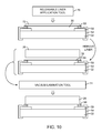
After edge portion 58E of dam structure 58 of FIG. 9 has been removed from layer 32, equipment of the type shown in FIG. 10 may be used to complete assembly operations. Equipment such as releasable liner application tool 70 may, if desired, be used to apply releasable liner layer 72 to the surface of solid pressure sensitive adhesive layer 36. Liner 72 may be formed from a flexible sheet of polymer and may be covered with a non-stick coating to facilitate release of liner 72 from adhesive layer 36. Tool 70 may include a manually and/or automatically controlled roller, a planar structure that presses liner 72 downwards against the surface of adhesive 36, or other liner attachment equipment.
Following application of liner 72, layer 32 may be transported to a desired location for finalizing assembly layers 26 and 32. The presence of liner 72 may help protect the surface of pressure sensitive adhesive layer 36 during transport.
Before attaching layer 26 to layer 32, liner 72 may be removed from pressure sensitive adhesive layer 36. Pressure sensitive adhesive lamination tool 74 (e.g., a tool such as tool 44 of FIG. 7) may then be used to perform lamination operations, thereby laminating layer 26 to layer 32. As shown at the bottom of FIG. 10, the resulting assembled structure includes upper layer 26, lower layer 32, and an interposed layer of pressure sensitive adhesive (layer 36).
Another illustrative approach for assembling layers 26 and 32 is shown in FIG. 11.
As shown in FIG. 11, dam attachment tool 56 may be used to attach dam structures 58 to layer 32 before application of adhesive 36.
Following attachment of dam structures 58, liquid adhesive application tool 60 may be used to apply liquid monomer pressure sensitive adhesive precursor material to the surface of layer 32. Because the precursor material is liquid, the precursor material will flow over structures 30 and will create a satisfactory conformal coating layer on the surface of layer 32.
Prior to curing, linear application tool 70 may be used to attach release liner 72 to layer 32 on top of liquid adhesive 36. Release liner 72 may be formed from a flexible sheet of polymer with a coating to prevent liner 72 from permanently sticking to adhesive 36. Liner 72 of FIG. 11 is preferably sufficiently transparent to ultraviolet light to allow ultraviolet light to pass through liner 72 to underlying adhesive 36 during curing operations.
To promote planarity in the surface of pressure sensitive adhesive layer 36, equipment 88 may press a planar member downwards onto the top of layer 72 and adhesive 36 during curing operations. Equipment 88 may be flattening (planarization) equipment such as manual or computer-controlled equipment that uses positioners 84 and clear plate 86 to press downwards on layer 72. Plate 86 may be formed from a layer of material such as fused silica, a layer of transparent ceramic, plastic, or glass, or other clear planar structure. When pressed downwards against the surface of adhesive layer 36, the surface of adhesive layer 36 may be planarized. While being flattened by plate 86 in this way, adhesive curing equipment such as ultraviolet light source 80 may be used to illuminate liquid adhesive layer 36 with ultraviolet light 82. Light 82 may pass through transparent plate 86 and release liner 72. The application of light 82 or other suitable curing stimulus (e.g., heat) may promote cross linking of the monomers in the liquid adhesive layer to form a solid polymer pressure sensitive adhesive layer such as layer 36 at the bottom of FIG. 11.
Assembly of layers 26 and 32 may then be completed using lamination tool 74, as shown in FIG. 10.
The assembled structures that include layers 26 and 32 (and any additional structures that are attached to these layers) may be assembled into finished electronic devices 10 such as devices 10 of FIGS. 1 and 2. Because thin pressure sensitive adhesive layers 36 and layers 36 that are not excessively soft may be used in attaching layers 26 and 32 together, devices 10 may be more compact and/or may contain stronger adhesive bonds than devices formed using conventional pressure sensitive adhesive lamination techniques.
If desired, trimming operations such as laser trimming operations may involve forming a cut in adhesive 36 that allows substantially all of dam structure 58 to be removed during trimming. This type of trimming operation is shown in FIG. 12.
Initially, dam structure 58 may be formed on layer (e.g., using dam attachment tool 56 of FIG. 11). Following attachment of dam structure 58, a dispensing tool such as liquid adhesive application tool 60 may be used to apply liquid monomer pressure sensitive adhesive precursor material to the surface of layer 32. Because the precursor material is liquid, the precursor material will flow over structures 30 and will create a satisfactory conformal coating layer on the surface of layer 32. Dam structure 58 may help contain the liquid adhesive material around the edges of layer 32.
Layer 36 may then be planarized and cured. For example, planarization operations may be performed using a pressurized liner of the type described in connection with FIG. 11. Curing may be performed using a UV lamp (e.g., lamp 80 of FIG. 11).
As part of the planarization process (e.g., when pressing downwards on liner 72 of FIG. 11, some of adhesive 36 may be forced laterally outward over the edge of dam structure 58, forming portion 36T of FIG. 12.
As shown in FIG. 12, a laser beam such as beam 100 may be applied using laser trimming equipment. The laser beam may be applied along the innermost edge of dam structure 58 to remove portion 102 of adhesive layer 36 (and possibly portions of the inner edge of dam structure 58). By cutting through adhesive layer 36, portion 36T of adhesive layer 36 and dam structure 58 may be trimmed away from the rest of layer 36. Following removal of the trimmed away portion of dam structure 58 and adhesive portion 36T, a trimmed version of layer 36 may remain on layer 32. Because dam structure 58 has been removed from layer 32, dam structure 58 will not interfere with subsequent lamination operations.
If desired, layer 36 may be planarized by depositing layer 36 in multiple thinner sublayers rather than a single layer. The use of multiple sublayers may help each sublayer flow to conform to underlying surface topology, resulting in a smooth flat surface for the resulting composite layer formed from the multiple sublayers.
The use of multilayer adhesive dispensing techniques to flatten layer 36 is illustrated in FIG. 13. In the example of FIG. 13, a first dispensing and curing cycle has been used to deposit adhesive layer 36A. Following formation of sublayer 36A, one or more additional liquid adhesive dispensing and curing operations may be used to form additional sublayers such as sublayer 36B. There may be, for example, two or more sublayer deposition cycles, three or more sublayer deposition cycles, four or more sublayer deposition cycles, etc. Sublayers may be dispensed using liquid adhesive application tools such as screen printing equipment, valves, etc. Curing may be performed using UV lamps or other equipment. Multilayer planarization operations of the type illustrated in FIG. 13 may be performed using equipment 38 and 40 of FIG. 7, may be used to perform flattening as described in connection with tool 48 of FIG. 8, may be used to implement the leveling and curing operations of tool 62 of FIG. 9, or may otherwise be used in flattening adhesive layer 36.
The foregoing is merely illustrative of the principles of this invention and various modifications can be made by those skilled in the art without departing from the scope and spirit of the invention.

Claims (22)

What is claimed is:
1. A method for assembling electronic device structures that include a first layer and a second layer, comprising:
dispensing a liquid pressure sensitive adhesive precursor material onto the first layer;
curing the liquid pressure sensitive adhesive precursor material using a curing tool to create a layer of pressure sensitive adhesive on the first layer;
following creation of the layer of pressure sensitive adhesive on the first layer, laminating the first and second layers together with the pressure sensitive adhesive so that the layer of pressure sensitive adhesive is interposed between the first and second layers, wherein the first layer comprises a surface on which an array of touch pad electrodes is formed, wherein the array of touch pad electrodes form a patterned set of surface structures on the first layer, wherein each touch pad electrode in the array of touch pad electrodes has respective first and second opposing surfaces, wherein the first surface is in direct contact with the first layer, and wherein the second surface is separated from the first layer by a step height, and wherein dispensing the liquid pressure sensitive adhesive precursor material comprises coating the surface of the first layer and the array of touch pad electrodes on the surface of the first layer with the liquid pressure sensitive adhesive precursor material; and
applying a dam structure to portions of the first layer, comprising:
using an adhesive to attach portions of the dam structure to the portions of the first layer, wherein the dam structure is configured to at least partly laterally confine the liquid pressure sensitive adhesive precursor material.
2. The method defined in claim 1 wherein laminating the first and second layers comprises vacuum laminating the first and second layers using pressure sensitive adhesive vacuum lamination equipment.
3. The method defined in claim 2 wherein the first and second layers comprise rigid layers and wherein laminating the first and second layers together comprises laminating the rigid layers together.
4. The method defined in claim 2 wherein the first and second layers comprise first and second display layers in a display and wherein laminating the first and second layers together comprises laminating the first and second display layers together.
5. The method defined in claim 1 wherein the first and second layers comprise touch pad layers and wherein laminating the first and second layers together comprises laminating the touch pad layers together.
6. The method defined in claim 1 wherein the first and second layers comprise rigid layers including at least one layer of glass, wherein laminating the first and second layers together comprises laminating the rigid layers together, wherein the curing tool comprises an ultraviolet light source, and wherein curing the liquid pressure sensitive adhesive precursor material using the curing tool to create the layer of pressure sensitive adhesive on the first layer comprises applying ultraviolet light to the layer of liquid pressure sensitive adhesive precursor material using the ultraviolet light source.
7. The method defined in claim 1 wherein the curing tool comprises an ultraviolet light source and wherein curing the liquid pressure sensitive adhesive precursor material using the curing tool to create the layer of pressure sensitive adhesive on the first layer comprises applying ultraviolet light to the layer of liquid pressure sensitive adhesive precursor material using the ultraviolet light source.
8. The method defined in claim 1 further comprising removing at least some of the dam structure using trimming equipment.
9. The method defined in claim 8 wherein removing at least some of the dam structure using the trimming equipment comprises removing the dam structure using laser trimming.
10. The method defined in claim 1 further comprising applying a release liner to the liquid pressure sensitive adhesive precursor material.
11. The method defined in claim 10 further comprising flattening the release liner with a planar member.
12. The method defined in claim 11 wherein curing the liquid pressure sensitive adhesive precursor material using the curing tool comprises applying ultraviolet light to the liquid pressure sensitive adhesive precursor material through the planar member and the release liner after the release liner is flattened with the planar member.
13. The method defined in claim 12 further comprising removing the release liner before laminating the first and second layers.
14. The method defined in claim 1 wherein dispensing the liquid pressure sensitive adhesive precursor material onto the first layer comprises applying the liquid pressure sensitive adhesive precursor material using equipment selected from the group consisting of: a valve, spraying equipment, and screen printing equipment.
15. The method defined in claim 1 further comprising flattening the pressure sensitive adhesive before laminating the first and second layers together with the pressure sensitive adhesive.
16. The method defined in claim 15 wherein flattening the pressure sensitive adhesive comprises applying heat to the dispensed liquid pressure sensitive adhesive precursor material.
17. The method defined in claim 1 wherein dispensing the liquid pressure sensitive adhesive precursor material onto the first layer and curing the liquid pressure sensitive adhesive precursor material using the curing tool to create the layer of pressure sensitive adhesive on the first layer comprises:
dispensing multiple sublayers of liquid pressure sensitive adhesive precursor material; and
curing each of the sublayers of liquid pressure sensitive adhesive precursor material to form the layer of pressure sensitive adhesive on the first layer.
18. A method of assembling first and second electronic device layers, wherein at least the first electronic device layer has surface structures, wherein the surface structures each have first and second opposing surfaces connected by third and fourth opposing surfaces, and wherein the third surface of each surface structure is in direct contact with the first electronic device layer, the method comprising:
applying a liquid pressure sensitive adhesive precursor material onto the first electronic device layer over the surface structures such that the liquid pressure sensitive adhesive precursor material directly contacts the first, second, and fourth surfaces of each surface structure;
forming a patterned layer of ink on the first electronic device layer, wherein applying the liquid pressure sensitive adhesive precursor material comprises coating the first electronic device layer and the patterned layer of ink on the first electronic device layer with the liquid pressure sensitive adhesive precursor material;
curing the liquid pressure sensitive adhesive precursor material to form a solid layer of pressure sensitive adhesive;
laminating the first and second electronic device layers together with the solid layer of pressure sensitive adhesive; and
applying a dam structure to portions of the first electronic device layer, comprising:
using an adhesive to attach portions of the dam structure to the portions of the first electronic device layer, wherein the dam structure is configured to at least partly laterally confine the liquid pressure sensitive adhesive precursor material.
19. The method defined in claim 18 wherein the first electronic device layer comprises a layer of glass and wherein curing the liquid pressure sensitive adhesive precursor material comprises applying ultraviolet light to the liquid pressure sensitive adhesive precursor material.
20. The method defined in claim 19 further comprising:
applying a release liner to the solid layer of pressure sensitive adhesive on the layer of glass.
21. The method defined in claim 9 wherein removing the dam structure using laser trimming further comprises removing the liquid pressure sensitive adhesive precursor material that has spread laterally outward over portions of the dam structure using laser trimming.
22. The method described in claim 18 wherein the surface structures are separated by gaps, and wherein the surface structures comprise touch sensor electrodes.
US13/329,010 2011-12-16 2011-12-16 Methods of joining device structures with adhesive Expired - Fee Related US9266310B2 (en)

Priority Applications (1)

Application Number Priority Date Filing Date Title
US13/329,010 US9266310B2 (en) 2011-12-16 2011-12-16 Methods of joining device structures with adhesive

Applications Claiming Priority (1)

Application Number Priority Date Filing Date Title
US13/329,010 US9266310B2 (en) 2011-12-16 2011-12-16 Methods of joining device structures with adhesive

Publications (2)

Publication Number Publication Date
US20130153128A1 US20130153128A1 (en) 2013-06-20
US9266310B2 true US9266310B2 (en) 2016-02-23

Family

ID=48608911

Family Applications (1)

Application Number Title Priority Date Filing Date
US13/329,010 Expired - Fee Related US9266310B2 (en) 2011-12-16 2011-12-16 Methods of joining device structures with adhesive

Country Status (1)

Country Link
US (1) US9266310B2 (en)

Cited By (18)

* Cited by examiner, † Cited by third party
Publication number Priority date Publication date Assignee Title
US10310686B2 (en) * 2016-07-11 2019-06-04 Apple Inc. Rigid trackpad for an electronic device
US10582631B2 (en) 2017-07-20 2020-03-03 Apple Inc. Housings formed from three-dimensional circuits
US20220168039A1 (en) * 2016-02-22 2022-06-02 Cilag Gmbh International Method of manufacturing a flexible circuit electrode for electrosurgical instrument
US11684412B2 (en) 2019-12-30 2023-06-27 Cilag Gmbh International Surgical instrument with rotatable and articulatable surgical end effector
US11696776B2 (en) 2019-12-30 2023-07-11 Cilag Gmbh International Articulatable surgical instrument
US11723716B2 (en) 2019-12-30 2023-08-15 Cilag Gmbh International Electrosurgical instrument with variable control mechanisms
US11751929B2 (en) 2016-01-15 2023-09-12 Cilag Gmbh International Modular battery powered handheld surgical instrument with selective application of energy based on tissue characterization
US11759251B2 (en) 2019-12-30 2023-09-19 Cilag Gmbh International Control program adaptation based on device status and user input
US11766287B2 (en) 2015-09-30 2023-09-26 Cilag Gmbh International Methods for operating generator for digitally generating electrical signal waveforms and surgical instruments
US11779387B2 (en) 2019-12-30 2023-10-10 Cilag Gmbh International Clamp arm jaw to minimize tissue sticking and improve tissue control
US11779329B2 (en) 2019-12-30 2023-10-10 Cilag Gmbh International Surgical instrument comprising a flex circuit including a sensor system
US11786291B2 (en) 2019-12-30 2023-10-17 Cilag Gmbh International Deflectable support of RF energy electrode with respect to opposing ultrasonic blade
US11812957B2 (en) 2019-12-30 2023-11-14 Cilag Gmbh International Surgical instrument comprising a signal interference resolution system
US11871982B2 (en) 2009-10-09 2024-01-16 Cilag Gmbh International Surgical generator for ultrasonic and electrosurgical devices
US11871955B2 (en) 2012-06-29 2024-01-16 Cilag Gmbh International Surgical instruments with articulating shafts
US11937863B2 (en) 2019-12-30 2024-03-26 Cilag Gmbh International Deflectable electrode with variable compression bias along the length of the deflectable electrode
US11944366B2 (en) 2019-12-30 2024-04-02 Cilag Gmbh International Asymmetric segmented ultrasonic support pad for cooperative engagement with a movable RF electrode
US11950797B2 (en) 2020-05-29 2024-04-09 Cilag Gmbh International Deflectable electrode with higher distal bias relative to proximal bias

Families Citing this family (5)

* Cited by examiner, † Cited by third party
Publication number Priority date Publication date Assignee Title
JP5899220B2 (en) * 2010-09-29 2016-04-06 ポスコ Method for manufacturing flexible electronic device using roll-shaped mother substrate, flexible electronic device, and flexible substrate
CN103246410B (en) * 2012-02-10 2016-04-06 瀚宇彩晶股份有限公司 The manufacture method of contact panel
CN104309267B (en) * 2014-09-17 2016-08-17 合肥鑫晟光电科技有限公司 A kind of method for bonding substrate, touch display substrate, display device
CN104461130A (en) * 2014-11-19 2015-03-25 业成光电(深圳)有限公司 Panel treating method
DE102019008780A1 (en) * 2019-12-18 2021-06-24 Kostal Automobil Elektrik Gmbh & Co. Kg Decorative functional component with a transparent partial surface

Citations (62)

* Cited by examiner, † Cited by third party
Publication number Priority date Publication date Assignee Title
US3823794A (en) * 1971-11-25 1974-07-16 Saint Gobain Acoustical panels
US4308296A (en) 1976-11-24 1981-12-29 Chitouras Costa G Method of curing particle-coated substrates
US4472124A (en) * 1980-09-05 1984-09-18 Matsushita Electric Industrial Co., Limited Device for producing an information recording disk
US5106441A (en) 1989-01-26 1992-04-21 Nokia Unterhaltungselektronik Method and jig for lcd-production
US5466325A (en) * 1993-06-02 1995-11-14 Nitto Denko Corporation Resist removing method, and curable pressure-sensitive adhesive, adhesive sheets and apparatus used for the method
US5530227A (en) * 1991-04-05 1996-06-25 The Boeing Company Method and apparatus for consolidating organic matrix composites using induction heating
US5541367A (en) 1994-10-31 1996-07-30 Dell Usa, L.P. Printed circuit board having a land with an inwardly facing surface and method for manufacturing same
US5771254A (en) 1996-01-25 1998-06-23 Hewlett-Packard Company Integrated controlled intensity laser-based light source
US5892203A (en) 1996-05-29 1999-04-06 International Business Machines Corporation Apparatus for making laminated integrated circuit devices
US5948175A (en) 1996-12-12 1999-09-07 Hughes Electronics Corporation Strap device clamping soldered wires for use in solar cell arrays
US5958447A (en) * 1998-03-17 1999-09-28 Plc Holding, L.L.C. Adhesive matrix type transdermal patch and method of manufacturing same
US6104565A (en) 1993-07-08 2000-08-15 Maxtor Corporation System architecture for hard disk drive
US6171105B1 (en) 1999-09-21 2001-01-09 Eg&G Ilc Technology, Inc. Dental-restoration light-curing system
US6249370B1 (en) 1998-09-18 2001-06-19 Ngk Insulators, Ltd. Display device
US20010038144A1 (en) * 2000-04-28 2001-11-08 Grigg Ford B. Interposers including upwardly protruding dams, semiconductor device assemblies including the interposers, and methods
US6319433B1 (en) 1999-09-14 2001-11-20 Invicta Corporation Composite ophthalmic lens remolding system for forming a lens therein
US20020005819A1 (en) 1993-10-22 2002-01-17 Peter A. Ronzani Head-mounted matrix display
US6376148B1 (en) 2001-01-17 2002-04-23 Nanotek Instruments, Inc. Layer manufacturing using electrostatic imaging and lamination
US6437669B1 (en) 2000-09-29 2002-08-20 Applied Micro Circuits Corporation Microwave to millimeter wave frequency substrate interface
US20030178134A1 (en) 2002-03-19 2003-09-25 Fujitsu Limited Apparatus and method for fabricating bonded substrate
US20040050485A1 (en) 2001-01-08 2004-03-18 Ulrich Speer Method and device for assembling substrates
US20040134603A1 (en) 2002-07-18 2004-07-15 Hideo Kobayashi Method and apparatus for curing adhesive between substrates, and disc substrate bonding apparatus
US20040238111A1 (en) 2003-01-09 2004-12-02 Con-Trol-Cure, Inc. UV LED control loop and controller for UV curing
US6867504B2 (en) 1996-09-06 2005-03-15 Hewlett-Packard Development Company, L.P. Method and apparatus for printed circuit board pads with registering feature for component leads
US20050139309A1 (en) * 2001-08-31 2005-06-30 Marc Savoie Method, apparatus and adhesive composition for ophthalmic lens blocking
US20050200371A1 (en) 2004-03-10 2005-09-15 Yakymyshyn Christopher P. Signal acquisition probing system using a micro-cavity laser
US20060022154A1 (en) 2004-07-29 2006-02-02 Schmitkons James W Shuttered lamp assembly and method of cooling the lamp assembly
US20060029784A1 (en) * 2004-08-09 2006-02-09 3M Innovative Properties Company Laminated optical article
US7012189B2 (en) 2001-03-28 2006-03-14 Apple Computer, Inc. Computer enclosure
US7033910B2 (en) 2001-09-12 2006-04-25 Reveo, Inc. Method of fabricating multi layer MEMS and microfluidic devices
US20060127594A1 (en) 2003-01-09 2006-06-15 Con-Trol-Cure, Inc. Light emitting apparatus and method for curing inks, coatings and adhesives
US20060137901A1 (en) 2004-12-29 2006-06-29 Gang Yu Electronic device including a substrate structure and a process for forming the same
US20060204670A1 (en) 2003-01-09 2006-09-14 Con-Trol-Cure, Inc. UV curing method and apparatus
US7135090B2 (en) 2002-10-25 2006-11-14 Ritdisplay Corporation FPD encapsulation apparatus and method for encapsulating the same
US20070026189A1 (en) 2005-07-28 2007-02-01 High Voltage Graphics, Inc. Flocked articles having noncompatible insert and porous film
US7195687B2 (en) 2001-04-11 2007-03-27 Sony Corporation Device transferring method, and device arraying method and image display unit fabricating method using the same
US20070187027A1 (en) 2006-02-16 2007-08-16 Delaware Capital Formation, Inc. Curing system and method of curing
US20070221978A1 (en) 2004-11-17 2007-09-27 Fujitsu Limited Semiconductor device
US7276132B2 (en) 1999-06-21 2007-10-02 Pella Corporation Method of making a reinforcing mat for a pultruded part
US20070254117A1 (en) 2006-05-01 2007-11-01 Bhret Graydon Conductive Stiffener for a Flexible Substrate
US20080023639A1 (en) 2004-07-22 2008-01-31 Lintec Corporation Ultraviolet Irradiation Apparatus
US20080038570A1 (en) * 2006-08-11 2008-02-14 Chisso Corporation Uv-curable ink-jet ink, electronic circuit board, electronic component and display device
US7351368B2 (en) 2002-07-03 2008-04-01 High Voltage Graphics, Inc. Flocked articles and methods of making same
US7372535B2 (en) 1999-05-24 2008-05-13 Sharp Kabushiki Kaisha Liquid crystal display and method of fabricating the same
US7427332B2 (en) 1998-01-27 2008-09-23 Ricoh Company, Ltd. Method and apparatus for assembling parts
US20080230177A1 (en) * 2007-03-19 2008-09-25 White Electronic Designs Corp. Enhanced liquid crystal display system and methods
US20090002338A1 (en) * 2007-06-27 2009-01-01 Masayoshi Kinoshita Screen input type image display
US20090032112A1 (en) 2004-07-23 2009-02-05 Afa Controls Llc Methods of Packaging Valve Chips and Related Valve Assemblies
US7498062B2 (en) 2004-05-26 2009-03-03 Wd Media, Inc. Method and apparatus for applying a voltage to a substrate during plating
US20090102882A1 (en) 2005-01-10 2009-04-23 Silverbrook Research Pty Ltd Mst device for attachment to surface with adhesive
US20090128518A1 (en) * 2007-11-15 2009-05-21 Hitachi Displays, Ltd. Screen-input image display device
US20090288756A1 (en) * 2008-05-21 2009-11-26 Manufacturing Resources International, Inc. Frame seal methods for lcd
US20090294692A1 (en) 2008-03-11 2009-12-03 Duke University Plasmonic assisted systems and methods for interior energy-activation from an exterior source
US20100026659A1 (en) 2008-07-30 2010-02-04 Flextronics Ap, Llc Glass substrate for capacitive touch panel and manufacturing method thereof
US20100134439A1 (en) 2008-11-21 2010-06-03 Hiroshi Ito Display device and manufacturing method thereof
US20100177032A1 (en) * 2009-01-09 2010-07-15 Seiko Epson Corporation Electrophoretic display device, electronic apparatus, and method of manufacturing electrophoretic display device
US20110012845A1 (en) 2009-07-20 2011-01-20 Rothkopf Fletcher R Touch sensor structures for displays
US20110292623A1 (en) 2010-05-28 2011-12-01 Craig Matthew Stanley Methods for assembling electronic devices by internally curing light-sensitive adhesive
US20120050958A1 (en) * 2010-08-27 2012-03-01 Emery Sanford Electronic devices with component mounting structures
US20120068353A1 (en) * 2010-09-20 2012-03-22 Stats Chippac, Ltd. Semiconductor Device and Method of Forming Dam Material With Openings Around Semiconductor Die for Mold Underfill Using Dispenser and Vacuum Assist
US8205327B2 (en) 2005-11-21 2012-06-26 Panasonic Corporation Method for manufacturing circuit board on which electronic component is mounted
US20120206376A1 (en) 2011-02-15 2012-08-16 Teh-Zheng Lin Transparent touch panel

Patent Citations (65)

* Cited by examiner, † Cited by third party
Publication number Priority date Publication date Assignee Title
US3823794A (en) * 1971-11-25 1974-07-16 Saint Gobain Acoustical panels
US4308296A (en) 1976-11-24 1981-12-29 Chitouras Costa G Method of curing particle-coated substrates
US4472124A (en) * 1980-09-05 1984-09-18 Matsushita Electric Industrial Co., Limited Device for producing an information recording disk
US5106441A (en) 1989-01-26 1992-04-21 Nokia Unterhaltungselektronik Method and jig for lcd-production
US5530227A (en) * 1991-04-05 1996-06-25 The Boeing Company Method and apparatus for consolidating organic matrix composites using induction heating
US5466325A (en) * 1993-06-02 1995-11-14 Nitto Denko Corporation Resist removing method, and curable pressure-sensitive adhesive, adhesive sheets and apparatus used for the method
US6104565A (en) 1993-07-08 2000-08-15 Maxtor Corporation System architecture for hard disk drive
US20020005819A1 (en) 1993-10-22 2002-01-17 Peter A. Ronzani Head-mounted matrix display
US5541367A (en) 1994-10-31 1996-07-30 Dell Usa, L.P. Printed circuit board having a land with an inwardly facing surface and method for manufacturing same
US5771254A (en) 1996-01-25 1998-06-23 Hewlett-Packard Company Integrated controlled intensity laser-based light source
US5892203A (en) 1996-05-29 1999-04-06 International Business Machines Corporation Apparatus for making laminated integrated circuit devices
US6867504B2 (en) 1996-09-06 2005-03-15 Hewlett-Packard Development Company, L.P. Method and apparatus for printed circuit board pads with registering feature for component leads
US5948175A (en) 1996-12-12 1999-09-07 Hughes Electronics Corporation Strap device clamping soldered wires for use in solar cell arrays
US7427332B2 (en) 1998-01-27 2008-09-23 Ricoh Company, Ltd. Method and apparatus for assembling parts
US5958447A (en) * 1998-03-17 1999-09-28 Plc Holding, L.L.C. Adhesive matrix type transdermal patch and method of manufacturing same
US6249370B1 (en) 1998-09-18 2001-06-19 Ngk Insulators, Ltd. Display device
US7372535B2 (en) 1999-05-24 2008-05-13 Sharp Kabushiki Kaisha Liquid crystal display and method of fabricating the same
US7276132B2 (en) 1999-06-21 2007-10-02 Pella Corporation Method of making a reinforcing mat for a pultruded part
US6319433B1 (en) 1999-09-14 2001-11-20 Invicta Corporation Composite ophthalmic lens remolding system for forming a lens therein
US6171105B1 (en) 1999-09-21 2001-01-09 Eg&G Ilc Technology, Inc. Dental-restoration light-curing system
US20010038144A1 (en) * 2000-04-28 2001-11-08 Grigg Ford B. Interposers including upwardly protruding dams, semiconductor device assemblies including the interposers, and methods
US6437669B1 (en) 2000-09-29 2002-08-20 Applied Micro Circuits Corporation Microwave to millimeter wave frequency substrate interface
US20040050485A1 (en) 2001-01-08 2004-03-18 Ulrich Speer Method and device for assembling substrates
US6376148B1 (en) 2001-01-17 2002-04-23 Nanotek Instruments, Inc. Layer manufacturing using electrostatic imaging and lamination
US7636244B2 (en) 2001-03-28 2009-12-22 Apple Inc. Computer enclosure
US7012189B2 (en) 2001-03-28 2006-03-14 Apple Computer, Inc. Computer enclosure
US7310872B2 (en) 2001-03-28 2007-12-25 Apple Inc. Computer enclosure
US7195687B2 (en) 2001-04-11 2007-03-27 Sony Corporation Device transferring method, and device arraying method and image display unit fabricating method using the same
US20050139309A1 (en) * 2001-08-31 2005-06-30 Marc Savoie Method, apparatus and adhesive composition for ophthalmic lens blocking
US7033910B2 (en) 2001-09-12 2006-04-25 Reveo, Inc. Method of fabricating multi layer MEMS and microfluidic devices
US20030178134A1 (en) 2002-03-19 2003-09-25 Fujitsu Limited Apparatus and method for fabricating bonded substrate
US7351368B2 (en) 2002-07-03 2008-04-01 High Voltage Graphics, Inc. Flocked articles and methods of making same
US20040134603A1 (en) 2002-07-18 2004-07-15 Hideo Kobayashi Method and apparatus for curing adhesive between substrates, and disc substrate bonding apparatus
US20070227670A1 (en) 2002-07-18 2007-10-04 Origin Electric Company, Limited Method and apparatus for curing adhesive between substrates, and disc substrate bonding apparatus
US7135090B2 (en) 2002-10-25 2006-11-14 Ritdisplay Corporation FPD encapsulation apparatus and method for encapsulating the same
US20060204670A1 (en) 2003-01-09 2006-09-14 Con-Trol-Cure, Inc. UV curing method and apparatus
US20040238111A1 (en) 2003-01-09 2004-12-02 Con-Trol-Cure, Inc. UV LED control loop and controller for UV curing
US20060127594A1 (en) 2003-01-09 2006-06-15 Con-Trol-Cure, Inc. Light emitting apparatus and method for curing inks, coatings and adhesives
US20050200371A1 (en) 2004-03-10 2005-09-15 Yakymyshyn Christopher P. Signal acquisition probing system using a micro-cavity laser
US7498062B2 (en) 2004-05-26 2009-03-03 Wd Media, Inc. Method and apparatus for applying a voltage to a substrate during plating
US20080023639A1 (en) 2004-07-22 2008-01-31 Lintec Corporation Ultraviolet Irradiation Apparatus
US20090032112A1 (en) 2004-07-23 2009-02-05 Afa Controls Llc Methods of Packaging Valve Chips and Related Valve Assemblies
US20060022154A1 (en) 2004-07-29 2006-02-02 Schmitkons James W Shuttered lamp assembly and method of cooling the lamp assembly
US20060029784A1 (en) * 2004-08-09 2006-02-09 3M Innovative Properties Company Laminated optical article
US20070221978A1 (en) 2004-11-17 2007-09-27 Fujitsu Limited Semiconductor device
US20060137901A1 (en) 2004-12-29 2006-06-29 Gang Yu Electronic device including a substrate structure and a process for forming the same
US20090102882A1 (en) 2005-01-10 2009-04-23 Silverbrook Research Pty Ltd Mst device for attachment to surface with adhesive
US20070026189A1 (en) 2005-07-28 2007-02-01 High Voltage Graphics, Inc. Flocked articles having noncompatible insert and porous film
US8205327B2 (en) 2005-11-21 2012-06-26 Panasonic Corporation Method for manufacturing circuit board on which electronic component is mounted
US20070187027A1 (en) 2006-02-16 2007-08-16 Delaware Capital Formation, Inc. Curing system and method of curing
US20070254117A1 (en) 2006-05-01 2007-11-01 Bhret Graydon Conductive Stiffener for a Flexible Substrate
US20080038570A1 (en) * 2006-08-11 2008-02-14 Chisso Corporation Uv-curable ink-jet ink, electronic circuit board, electronic component and display device
US20080230177A1 (en) * 2007-03-19 2008-09-25 White Electronic Designs Corp. Enhanced liquid crystal display system and methods
US20090002338A1 (en) * 2007-06-27 2009-01-01 Masayoshi Kinoshita Screen input type image display
US20090128518A1 (en) * 2007-11-15 2009-05-21 Hitachi Displays, Ltd. Screen-input image display device
US20090294692A1 (en) 2008-03-11 2009-12-03 Duke University Plasmonic assisted systems and methods for interior energy-activation from an exterior source
US20090288756A1 (en) * 2008-05-21 2009-11-26 Manufacturing Resources International, Inc. Frame seal methods for lcd
US20100026659A1 (en) 2008-07-30 2010-02-04 Flextronics Ap, Llc Glass substrate for capacitive touch panel and manufacturing method thereof
US20100134439A1 (en) 2008-11-21 2010-06-03 Hiroshi Ito Display device and manufacturing method thereof
US20100177032A1 (en) * 2009-01-09 2010-07-15 Seiko Epson Corporation Electrophoretic display device, electronic apparatus, and method of manufacturing electrophoretic display device
US20110012845A1 (en) 2009-07-20 2011-01-20 Rothkopf Fletcher R Touch sensor structures for displays
US20110292623A1 (en) 2010-05-28 2011-12-01 Craig Matthew Stanley Methods for assembling electronic devices by internally curing light-sensitive adhesive
US20120050958A1 (en) * 2010-08-27 2012-03-01 Emery Sanford Electronic devices with component mounting structures
US20120068353A1 (en) * 2010-09-20 2012-03-22 Stats Chippac, Ltd. Semiconductor Device and Method of Forming Dam Material With Openings Around Semiconductor Die for Mold Underfill Using Dispenser and Vacuum Assist
US20120206376A1 (en) 2011-02-15 2012-08-16 Teh-Zheng Lin Transparent touch panel

Non-Patent Citations (5)

* Cited by examiner, † Cited by third party
Title
Anders et al., "Conductive Adhesives vs Solder Paste: A Comparative Life Cycle Based Screening, Abstract", Advances in Life Cycle Engineering for Sustainable Manufacturing, 2007 (p. 285).
Glaser, "Colorants and Special Additives for Laser Welding", Joining Plastics 2006, Apr. 25-26, 2006 (5 pages).
Hill et al., U.S. Appl. No. 12/753,005, filed Apr. 1, 2010.
Krogdahl et al., U.S. Appl. No. 13/567,949, Aug. 6, 2012.
Zadeskey, U.S. Appl. No. 12/571,295, filed Sep. 30, 2009.

Cited By (21)

* Cited by examiner, † Cited by third party
Publication number Priority date Publication date Assignee Title
US11871982B2 (en) 2009-10-09 2024-01-16 Cilag Gmbh International Surgical generator for ultrasonic and electrosurgical devices
US11871955B2 (en) 2012-06-29 2024-01-16 Cilag Gmbh International Surgical instruments with articulating shafts
US11766287B2 (en) 2015-09-30 2023-09-26 Cilag Gmbh International Methods for operating generator for digitally generating electrical signal waveforms and surgical instruments
US11896280B2 (en) 2016-01-15 2024-02-13 Cilag Gmbh International Clamp arm comprising a circuit
US11751929B2 (en) 2016-01-15 2023-09-12 Cilag Gmbh International Modular battery powered handheld surgical instrument with selective application of energy based on tissue characterization
US20220168039A1 (en) * 2016-02-22 2022-06-02 Cilag Gmbh International Method of manufacturing a flexible circuit electrode for electrosurgical instrument
US10310686B2 (en) * 2016-07-11 2019-06-04 Apple Inc. Rigid trackpad for an electronic device
US10582631B2 (en) 2017-07-20 2020-03-03 Apple Inc. Housings formed from three-dimensional circuits
US11707318B2 (en) 2019-12-30 2023-07-25 Cilag Gmbh International Surgical instrument with jaw alignment features
US11759251B2 (en) 2019-12-30 2023-09-19 Cilag Gmbh International Control program adaptation based on device status and user input
US11779387B2 (en) 2019-12-30 2023-10-10 Cilag Gmbh International Clamp arm jaw to minimize tissue sticking and improve tissue control
US11779329B2 (en) 2019-12-30 2023-10-10 Cilag Gmbh International Surgical instrument comprising a flex circuit including a sensor system
US11786294B2 (en) 2019-12-30 2023-10-17 Cilag Gmbh International Control program for modular combination energy device
US11786291B2 (en) 2019-12-30 2023-10-17 Cilag Gmbh International Deflectable support of RF energy electrode with respect to opposing ultrasonic blade
US11812957B2 (en) 2019-12-30 2023-11-14 Cilag Gmbh International Surgical instrument comprising a signal interference resolution system
US11723716B2 (en) 2019-12-30 2023-08-15 Cilag Gmbh International Electrosurgical instrument with variable control mechanisms
US11696776B2 (en) 2019-12-30 2023-07-11 Cilag Gmbh International Articulatable surgical instrument
US11684412B2 (en) 2019-12-30 2023-06-27 Cilag Gmbh International Surgical instrument with rotatable and articulatable surgical end effector
US11937863B2 (en) 2019-12-30 2024-03-26 Cilag Gmbh International Deflectable electrode with variable compression bias along the length of the deflectable electrode
US11944366B2 (en) 2019-12-30 2024-04-02 Cilag Gmbh International Asymmetric segmented ultrasonic support pad for cooperative engagement with a movable RF electrode
US11950797B2 (en) 2020-05-29 2024-04-09 Cilag Gmbh International Deflectable electrode with higher distal bias relative to proximal bias

Also Published As

Publication number Publication date
US20130153128A1 (en) 2013-06-20

Similar Documents

Publication Publication Date Title
US9266310B2 (en) Methods of joining device structures with adhesive
KR102195371B1 (en) Curve laminating device and laminating method thereof
US20070069418A1 (en) In mold manufacturing of an object comprising a functional element
CN109873020B (en) Laminated film material, display panel, display device and preparation method of display panel
US20160361907A1 (en) Method for bonding substrates, touch substrate and display device
TW201239465A (en) Image display panel and manufacturing method thereof
JP6322871B2 (en) Flexographic printing plate and manufacturing method thereof, and manufacturing method of liquid crystal display element
CN104540672B (en) Layered product including adhesive layer and preparation method thereof
CN104199574A (en) Integrated piece, manufacturing method thereof and method for manufacturing touch screen by adoption of integrated piece
TW201539279A (en) Laminate, method for producing laminate, capacitive touch panel and image display device
JP6321729B2 (en) Circuit board structure and manufacturing method thereof
JP5245003B1 (en) Decorative film and method for producing the same
CN113314031B (en) Display panel and preparation method thereof
CN107678583A (en) A kind of preparation technology of 3D textures handset touch panel
US20200324536A1 (en) Film laminator for cell phones
KR20130075869A (en) Panel laminating method and cutting method thereof
US10336048B1 (en) Film laminator for cell phones
JP5707176B2 (en) Decorative transparent substrate and method for producing the same
TW201537429A (en) Laminate, method for producing laminate, capacitive touch panel and image display device
JP6306715B2 (en) Method for producing flexographic printing plate and method for producing liquid crystal display element
TWM337793U (en) Fully planar touch panel
KR101560473B1 (en) Manufacturing apparatus and method for a cliche of Metal-Mesh
CN116939472B (en) Manufacturing process of directional sound-emitting screen
CN110197838A (en) Manufacturing method, display panel and the display device of display panel
JP2005309021A (en) Method for manufacturing display panel and transparent tacky adhesive sheet

Legal Events

Date Code Title Description
AS Assignment

Owner name: APPLE INC., CALIFORNIA

Free format text: ASSIGNMENT OF ASSIGNORS INTEREST;ASSIGNORS:KROGDAHL, JAMES R.;CUSEO, JAMES M.;SIGNING DATES FROM 20111117 TO 20111118;REEL/FRAME:027399/0643

FEPP Fee payment procedure

Free format text: PAYOR NUMBER ASSIGNED (ORIGINAL EVENT CODE: ASPN); ENTITY STATUS OF PATENT OWNER: LARGE ENTITY

STCF Information on status: patent grant

Free format text: PATENTED CASE

FEPP Fee payment procedure

Free format text: MAINTENANCE FEE REMINDER MAILED (ORIGINAL EVENT CODE: REM.); ENTITY STATUS OF PATENT OWNER: LARGE ENTITY

LAPS Lapse for failure to pay maintenance fees

Free format text: PATENT EXPIRED FOR FAILURE TO PAY MAINTENANCE FEES (ORIGINAL EVENT CODE: EXP.); ENTITY STATUS OF PATENT OWNER: LARGE ENTITY

STCH Information on status: patent discontinuation

Free format text: PATENT EXPIRED DUE TO NONPAYMENT OF MAINTENANCE FEES UNDER 37 CFR 1.362

FP Lapsed due to failure to pay maintenance fee

Effective date: 20200223