US9246409B2 - Method and apparatus for controlling LCL converters using asymmetric voltage cancellation techniques - Google Patents
Method and apparatus for controlling LCL converters using asymmetric voltage cancellation techniques Download PDFInfo
- Publication number
- US9246409B2 US9246409B2 US13/642,925 US201213642925A US9246409B2 US 9246409 B2 US9246409 B2 US 9246409B2 US 201213642925 A US201213642925 A US 201213642925A US 9246409 B2 US9246409 B2 US 9246409B2
- Authority
- US
- United States
- Prior art keywords
- inductor
- circuit
- combination
- points
- control
- Prior art date
- Legal status (The legal status is an assumption and is not a legal conclusion. Google has not performed a legal analysis and makes no representation as to the accuracy of the status listed.)
- Expired - Fee Related, expires
Links
- 238000000034 method Methods 0.000 title claims abstract description 60
- 230000002441 reversible effect Effects 0.000 claims description 67
- 238000011084 recovery Methods 0.000 claims description 62
- 239000003990 capacitor Substances 0.000 claims description 22
- 238000012546 transfer Methods 0.000 claims description 21
- 230000001939 inductive effect Effects 0.000 claims description 15
- 238000004891 communication Methods 0.000 claims description 2
- 238000012544 monitoring process Methods 0.000 claims 6
- 230000004044 response Effects 0.000 abstract description 5
- 230000001052 transient effect Effects 0.000 abstract description 5
- 230000033228 biological regulation Effects 0.000 abstract description 2
- 238000013461 design Methods 0.000 description 15
- 239000011159 matrix material Substances 0.000 description 15
- 230000007704 transition Effects 0.000 description 12
- 238000004458 analytical method Methods 0.000 description 10
- 238000010586 diagram Methods 0.000 description 10
- 230000008901 benefit Effects 0.000 description 8
- 230000006870 function Effects 0.000 description 8
- 238000013459 approach Methods 0.000 description 6
- 238000005259 measurement Methods 0.000 description 6
- 230000008569 process Effects 0.000 description 6
- 238000006243 chemical reaction Methods 0.000 description 4
- 230000006872 improvement Effects 0.000 description 4
- 238000004519 manufacturing process Methods 0.000 description 4
- 230000003071 parasitic effect Effects 0.000 description 4
- 230000008859 change Effects 0.000 description 3
- 230000000694 effects Effects 0.000 description 3
- 238000001914 filtration Methods 0.000 description 3
- 230000005355 Hall effect Effects 0.000 description 2
- 230000008878 coupling Effects 0.000 description 2
- 238000010168 coupling process Methods 0.000 description 2
- 238000005859 coupling reaction Methods 0.000 description 2
- 238000000354 decomposition reaction Methods 0.000 description 2
- 238000001514 detection method Methods 0.000 description 2
- 230000001965 increasing effect Effects 0.000 description 2
- 239000000463 material Substances 0.000 description 2
- 238000012935 Averaging Methods 0.000 description 1
- 241000874889 Euphilotes enoptes Species 0.000 description 1
- 230000003750 conditioning effect Effects 0.000 description 1
- 238000011217 control strategy Methods 0.000 description 1
- 230000007423 decrease Effects 0.000 description 1
- 230000003247 decreasing effect Effects 0.000 description 1
- 238000012938 design process Methods 0.000 description 1
- 230000004069 differentiation Effects 0.000 description 1
- 238000005516 engineering process Methods 0.000 description 1
- 238000011156 evaluation Methods 0.000 description 1
- 238000009472 formulation Methods 0.000 description 1
- 230000010354 integration Effects 0.000 description 1
- 230000002452 interceptive effect Effects 0.000 description 1
- 238000002955 isolation Methods 0.000 description 1
- 238000012804 iterative process Methods 0.000 description 1
- 238000013507 mapping Methods 0.000 description 1
- 239000000203 mixture Substances 0.000 description 1
- 238000012986 modification Methods 0.000 description 1
- 230000004048 modification Effects 0.000 description 1
- 238000005457 optimization Methods 0.000 description 1
- 230000009467 reduction Effects 0.000 description 1
- 230000002829 reductive effect Effects 0.000 description 1
- 238000011160 research Methods 0.000 description 1
- 230000000717 retained effect Effects 0.000 description 1
- 230000000630 rising effect Effects 0.000 description 1
- 230000035945 sensitivity Effects 0.000 description 1
- 238000004088 simulation Methods 0.000 description 1
- 230000005476 size effect Effects 0.000 description 1
- 238000010183 spectrum analysis Methods 0.000 description 1
- 235000013599 spices Nutrition 0.000 description 1
- 238000012360 testing method Methods 0.000 description 1
Images


Classifications
-
- H—ELECTRICITY
- H02—GENERATION; CONVERSION OR DISTRIBUTION OF ELECTRIC POWER
- H02M—APPARATUS FOR CONVERSION BETWEEN AC AND AC, BETWEEN AC AND DC, OR BETWEEN DC AND DC, AND FOR USE WITH MAINS OR SIMILAR POWER SUPPLY SYSTEMS; CONVERSION OF DC OR AC INPUT POWER INTO SURGE OUTPUT POWER; CONTROL OR REGULATION THEREOF
- H02M7/00—Conversion of ac power input into dc power output; Conversion of dc power input into ac power output
- H02M7/42—Conversion of dc power input into ac power output without possibility of reversal
- H02M7/44—Conversion of dc power input into ac power output without possibility of reversal by static converters
- H02M7/48—Conversion of dc power input into ac power output without possibility of reversal by static converters using discharge tubes with control electrode or semiconductor devices with control electrode
- H02M7/53—Conversion of dc power input into ac power output without possibility of reversal by static converters using discharge tubes with control electrode or semiconductor devices with control electrode using devices of a triode or transistor type requiring continuous application of a control signal
- H02M7/537—Conversion of dc power input into ac power output without possibility of reversal by static converters using discharge tubes with control electrode or semiconductor devices with control electrode using devices of a triode or transistor type requiring continuous application of a control signal using semiconductor devices only, e.g. single switched pulse inverters
- H02M7/5387—Conversion of dc power input into ac power output without possibility of reversal by static converters using discharge tubes with control electrode or semiconductor devices with control electrode using devices of a triode or transistor type requiring continuous application of a control signal using semiconductor devices only, e.g. single switched pulse inverters in a bridge configuration
- H02M7/53871—Conversion of dc power input into ac power output without possibility of reversal by static converters using discharge tubes with control electrode or semiconductor devices with control electrode using devices of a triode or transistor type requiring continuous application of a control signal using semiconductor devices only, e.g. single switched pulse inverters in a bridge configuration with automatic control of output voltage or current
-
- H—ELECTRICITY
- H02—GENERATION; CONVERSION OR DISTRIBUTION OF ELECTRIC POWER
- H02J—CIRCUIT ARRANGEMENTS OR SYSTEMS FOR SUPPLYING OR DISTRIBUTING ELECTRIC POWER; SYSTEMS FOR STORING ELECTRIC ENERGY
- H02J50/00—Circuit arrangements or systems for wireless supply or distribution of electric power
- H02J50/10—Circuit arrangements or systems for wireless supply or distribution of electric power using inductive coupling
- H02J50/12—Circuit arrangements or systems for wireless supply or distribution of electric power using inductive coupling of the resonant type
-
- H02J5/005—
-
- H02M2007/4815—
-
- H—ELECTRICITY
- H02—GENERATION; CONVERSION OR DISTRIBUTION OF ELECTRIC POWER
- H02M—APPARATUS FOR CONVERSION BETWEEN AC AND AC, BETWEEN AC AND DC, OR BETWEEN DC AND DC, AND FOR USE WITH MAINS OR SIMILAR POWER SUPPLY SYSTEMS; CONVERSION OF DC OR AC INPUT POWER INTO SURGE OUTPUT POWER; CONTROL OR REGULATION THEREOF
- H02M7/00—Conversion of ac power input into dc power output; Conversion of dc power input into ac power output
- H02M7/42—Conversion of dc power input into ac power output without possibility of reversal
- H02M7/44—Conversion of dc power input into ac power output without possibility of reversal by static converters
- H02M7/48—Conversion of dc power input into ac power output without possibility of reversal by static converters using discharge tubes with control electrode or semiconductor devices with control electrode
- H02M7/4815—Resonant converters
-
- Y—GENERAL TAGGING OF NEW TECHNOLOGICAL DEVELOPMENTS; GENERAL TAGGING OF CROSS-SECTIONAL TECHNOLOGIES SPANNING OVER SEVERAL SECTIONS OF THE IPC; TECHNICAL SUBJECTS COVERED BY FORMER USPC CROSS-REFERENCE ART COLLECTIONS [XRACs] AND DIGESTS
- Y02—TECHNOLOGIES OR APPLICATIONS FOR MITIGATION OR ADAPTATION AGAINST CLIMATE CHANGE
- Y02B—CLIMATE CHANGE MITIGATION TECHNOLOGIES RELATED TO BUILDINGS, e.g. HOUSING, HOUSE APPLIANCES OR RELATED END-USER APPLICATIONS
- Y02B70/00—Technologies for an efficient end-user side electric power management and consumption
- Y02B70/10—Technologies improving the efficiency by using switched-mode power supplies [SMPS], i.e. efficient power electronics conversion e.g. power factor correction or reduction of losses in power supplies or efficient standby modes
-
- Y02B70/1441—
Definitions
- the present disclosure relates to a method for improving the efficiency of inductive power transfer systems, and in particular, to controlling LCL resonant converters using asymmetric voltage cancellation techniques.
- IPT Inductive Power Transfer
- input power in the form of electrical energy from a constant high frequency alternating current
- FIG. 1 the magnetic field
- the magnetic field is transformed into an induced voltage according to Faraday's Law, thus creating output power for the load.
- Wireless power transfer may enable electric vehicles to be continuously charged while stationary or in motion with no physical connection between the vehicle and the roadway.
- IPT systems may be broadly separated into three main categories, including the power supply, magnetic coupler and the pickup receiver.
- a key to designing wireless power supplies is to convert the DC power to high frequency AC power with no or little loss and parasitic effect while keeping the cost and size low as well. In practice, zero loss is never achieved. Hence, the objective of designing power converters has been to obtain the highest possible conversion efficiency, while keeping cost, size, and parasitic effects like Electromagnetic Interference (EMI) to a minimum. Improving efficiency and reducing EMI of high-power Inductor Capacitor Inductor (LCL) resonant converters has become a significant undertaking in the area of wireless power transfer. Electrical efficiency issues are associated with conversion loss in the transmitter electronics.
- EMI Electromagnetic Interference
- MOSFET technology has grown rapidly over the past decade in their performance. These devices are used as the fundamental building block for many power electronic systems today. However, the body diode in such devices usually has very poor turn off characteristics causing huge diode reverse recovery losses especially reported in LCL converters. What is needed is a control strategy for LCL converters to improve efficiency. This includes optimal switching conditions to eliminate diode reverse recovery losses in LCL converters. Fast switching speeds and very low on state resistance of MOSFET's is needed to improve insulated gate bipolar transistor (IGBT) performance.
- IGBT insulated gate bipolar transistor
- AVC Asymmetric Voltage Cancellation
- IPT Inductive Power Transfer
- AVC control provides a way to avoid diode reverse recovery losses while achieving acceptable Total Harmonic Distortion (THD) and associated losses. Coupled with extra parasitic or external capacitance across the switches in the H-bridge, a fully soft switched Zero Voltage Switching (ZVS) fixed frequency resonant power converter is realized.
- ZVS Zero Voltage Switching
- FIG. 1 illustrates an inductive power transfer system
- FIG. 2 illustrates an exemplary LCL resonant converter with full bridge control.
- FIG. 3 illustrates a map of an exemplary switch gate waveform to H-bridge output voltage.
- FIG. 4 illustrates a table with various, exemplary switching transition states for H-bridge.
- FIG. 5 illustrates an exemplary symmetric voltage cancellation control Vab waveform.
- FIG. 6 illustrates an exemplary asymmetric duty cycle control Vab waveform.
- FIG. 7 illustrates an exemplary asymmetric voltage cancellation control Vab waveform.
- FIG. 11 illustrates an exemplary LCL converter using a Current Transformer (CT) to detect bridge current.
- CT Current Transformer
- FIG. 16 illustrates the relation of the N order as a function of quality factor.
- FIG. 17 illustrates an exemplary flowchart for determining diode reverse recovery loss.
- FIG. 18 illustrates an exemplary schematic of the Greedy salesperson algorithm.
- FIG. 24 illustrates an exemplary solution of the Greedy sales person algorithm with a minimum THD path.
- FIG. 25 illustrates the 4th order polynomial fitting for beta angle.
- FIG. 26 illustrates bridge inductor current measurement sensing with a resistor or Hall Effect sensor.
- FIG. 27 illustrates an exemplary phase detection circuit using PLL.
- FIG. 28 illustrates an exemplary filtered bridge current waveform.
- FIG. 29 illustrates a block diagram of an exemplary measuring circuit.
- FIG. 30 illustrates an exemplary microcontroller input output signal diagram implementation of controller.
- FIG. 31 illustrates an exemplary internal block diagram for a microcontroller implementation of AVC.
- FIG. 32 illustrates an exemplary block diagram for designing an AVC controller.
- FIG. 33 illustrates an exemplary soft switched fixed frequency LCL converter with extra switch output capacitance.
- FIG. 34 illustrates an exemplary flowchart for determining switching capacitance values.
- FIG. 35 illustrates various, exemplary bridge currents at the instances of switching.
- FIG. 36 illustrates a table of exemplary component values for an LCL resonant network.
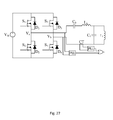
- FIG. 37 illustrates an exemplary high-level control block diagram.
- FIG. 38 illustrates a low-level schematic of an exemplary H-bridge half driver.
- FIG. 39 illustrates an exemplary current path through the disclosed system.
- FIG. 40 illustrates a high-level schematic of an exemplary LCL converter system.
- FIG. 41 illustrates a schematic of an exemplary LCL resonant network.
- FIG. 42 illustrates an exemplary software flow diagram.
- FIG. 43 illustrates an example of an exemplary Graphical User Interface (GUI).
- GUI Graphical User Interface
- FIG. 44 illustrates a flow diagram of an exemplary Hardware Description Language (HDL) design logic.
- HDL Hardware Description Language
- FIG. 45 illustrates a table listing the total harmonic distortion improvements in an exemplary asymmetric voltage cancellation.
- FIG. 46 illustrates exemplary experimental results showing that diode reverse recovery may not be avoided.
- FIG. 47 illustrates exemplary experimental results showing that diode reverse recovery may be avoided.
- FIG. 48 illustrates an exemplary efficiency comparison of asymmetric voltage cancellation vs. symmetric voltage cancellation.
- the present disclosure describes a method and apparatus for an improved Inductor Capacitor Inductor (LCL) resonant converter.
- An LCL network is tuned for resonance at a desired frequency.
- LCL networks operated at resonance act as a constant AC power source.
- An LCL converter is usually inefficient due to diode reverse recovery loss, which is associated with the reverse bias of the body diode while in the conduction state. This results in high switching losses.
- the converter efficiency is also related to the loading range in which a normal operating quality factor (Q 1 ) values makes it impossible to avoid diode reverse recovery loss.
- Q 1 can be defined by the equation below:
- LCL resonant converters include Symmetric Voltage Cancellation (SVC) and Asymmetric Duty Cycle (ADC) techniques. Both of these methods utilize a single control variable.
- SVC Symmetric Voltage Cancellation
- ADC Asymmetric Duty Cycle
- the present disclosure introduces Asymmetric Voltage Cancellation (AVC), which takes advantage of three control variables for greater flexibility over SVC and ADC. This allows for control equivalent to SVC and ADC plus additional flexibility, thus by nature, AVC should be no less efficient than SVC and ADC for LCL resonant converter control.
- Other converters such as the full bridge series resonant converter have used AVC; however, the inventors are not aware of the application of AVC into LCL converters.
- EMI Electromagnetic Interference
- TDD Total Harmonic Distortion
- the LCL resonant converter as shown in FIG. 2 is a well-known circuit that takes a DC input and produces a high frequency AC output.
- a desirable attribute of the LCL resonant converter is that when tuned and operated at its resonant frequency, the output current remains constant regardless of the load placed on it. This means the AC output current may be controlled without knowing the load, e.g. constant current source property.
- LCL converters have the advantages of high efficiency at light load (unity power factor) and harmonic filtering capabilities.
- LCL resonant converters have a problem in their full-bridge control.
- the diodes in the full-bridge controller are prone to the high switching losses known as diode reverse recovery loss.
- Diode reverse recovery loss occurs when a diode, which is forward biased, has an instantaneous voltage transition in the negative direction while current is still flowing through it.
- the transition from state S 1 to state S 2 can be described with reference to FIGS. 2-4 .
- the current i b is negative in S 1
- the state is known as S 1b .
- the current is flowing up through D 1 and D 4 , and V ab is positive. Since V g1 is high, and V g2 is low, there is no voltage across D 4 in the reverse direction.
- V g1 is high, and V g2 is low, there is no voltage across D 4 in the reverse direction.
- D 4 will transition to a non-conduction state as current starts flowing through the channel of the MOSFET associated with V g2 , but for a moment D 4 is conducting with a high reverse bias voltage.
- This phenomenon is called diode reverse recovery loss and the associated switching loss can be tens to hundreds of times of that in conduction losses for some components like power MOSFETs, which typically have particularly poor performance body diodes. This is due to the inherently poor characteristics of the body diode in the MOSFET during manufacturing.
- the current methods to avoid this problem are to place passive diode components (with excellent reverse recovery response) in parallel with the body diode, or to use ADC control.
- the former increases both the cost and size of the circuit and the later introduces increased harmonics into the waveform, hence increasing the THD.
- a first method used to control current is SVC control (see FIG. 5 ).
- SVC control is very easy to implement because it only uses one control variable, namely the conduction angle ⁇ (180°-alpha).
- SVC control also provides low THD because a conduction angle at 120° eliminates all third harmonic components and the symmetry eliminates all even harmonics.
- Q 1 operating quality factor
- a second method used to control LCL resonant converters is ADC control (see FIG. 6 ).
- This method has the advantages of being easy to implement and avoids diode reverse recovery loss above a certain quality factor.
- ADC Like SVC, ADC only has one control variable, beta. However, it has much higher THD because of the asymmetric waveform.
- AVC control provides a solution (see FIG. 7 ) that is able to control the AC input to the LCL resonant converter while reducing diode reverse recovery loss.
- AVC control uses three variables of control namely, alpha+, beta and alpha ⁇ . It has the potential to have the combined benefits of SVC and ADC by reducing THD and avoiding diode reverse recovery loss.
- AVC control is much more difficult to implement because of the three control variables involved. Additionally, to achieve the best results, the load condition (Q 1 ) and gamma (Lb/L 1 ) of the LCL resonant converter should be considered (discussed further in sections 3 and 4 ). In addition, the reflected reactive impedance from the secondary pickup also should be considered, as will be shown later, as not all reactive loading can be compensated passively, especially in systems that exhibit variable mutual coupling conditions. Variable mutual coupling systems in inductive power transfer systems have variable heights and alignments between transmitter and receiver coils. Examples of these systems include stationary EV charging systems where drivers cannot undertake perfect parking alignment positions and power transfer to vehicles in motion.
- an optimal AVC control algorithm may find the trajectory for the three variables, alpha+, beta, alpha ⁇ that will satisfy the avoidance of diode reverse recovery loss, under different Q 1 , gamma (Lb/L 1 ), reflected impedance, and component sensitivity issues.
- Q 1 Q 1
- gamma Lb/L 1
- reflected impedance reflected impedance
- component sensitivity issues Unfortunately, the problem is extremely complicated as there are many combinations of alpha+, beta, and alpha ⁇ that may satisfy this condition and determining the optimal solution is not simple.
- Some basic guidelines that may govern the optimal solution are THD, switching losses (not diode reverse recovery losses), and conduction losses.
- a steady-state time domain analysis approach may be used to solve for the solutions of AVC.
- This embodiment uses state-space representation in each switching state to solve for a single period waveform of V ab , i b , and i 1 .
- a waveform solution using this approach has also been verified using SPICE modeling.
- ⁇ ⁇ B [ 1 ⁇ / ⁇ L b 0 0 0 ] ( 3 )
- Solving (7) will give the state vector condition at each time interval. Substituting the state vector as initial conditions into (6) provides the full time domain solution.
- the control variables Beta, Alpha+, and Alpha ⁇ , and the circuit characteristics Lb, Cb, L 1 , C 1 , and Zr, as shown in FIG. 2 are used in an algorithm.
- the algorithm is made to iterate through the possible combinations of Beta, Alpha+, and Alpha ⁇ , along with many Q 1 values (loading conditions) and fills four matrices for i 1 , ib, total harmonic distortion of i 1 , and total harmonic distortion of ib. If the combination avoids diode reverse recovery loss then the corresponding points in the matrices are filled with the root-mean square i 1 , and ib values, and the total harmonic distortion values. Also, the switching current at all switching transitions and the conduction current for each state are saved.
- the accumulated THD data may be displayed in an acceptability matrix, as shown in FIG. 8 .
- FIG. 9 is an acceptability matrix, which may be compared to FIG. 8 to illustrate the effect of decreasing the Q 1 value.
- the acceptability matrices clearly show that SVC control fails to avoid diode reverse recovery loss.
- a separate acceptability matrix is constructed for each different beta value, the evaluation of the acceptability matrices shows that ADC control avoids diode reverse recovery loss.
- FIG. 10 is another acceptability matrix, which may be compared to FIGS. 8 and 9 to illustrate the effect of changing beta.
- the hardware was designed for a maximum primary track current (i 1 ) of 6.57 A RMS, and a ratio L b /L 1 of 1.5 as shown in FIG. 36 .
- i 1 maximum primary track current
- L b /L 1 ratio of 1.5 as shown in FIG. 36 .
- V dc 2 ⁇ 2 ⁇ V dc ⁇ ⁇ ( I 1 ) max ( 8 ) where V dc is the input DC voltage to the H-bridge.
- the inductance and capacitance values can be determined using,
- gamma is an important parameter in the design of a system in which diode reverse recovery loss is avoided.
- the smaller the ratio L b /L 1 the larger the regions over which diode reverse recovery loss may be avoided.
- the minimum ratio that may be obtained is 1 as C b cannot be larger than infinity.
- a ratio of 1.5 is large enough to keep the circuit realizable (with acceptable value of C b ), and small enough to give usable regions for diode reverse recovery avoidance.
- FIG. 11 shows a listing of values that may be used. The inductors are custom tuned to obtain desired values, and the capacitors are in banks giving the flexibility to fine tune.
- an optimal trajectory that avoids diode reverse recovery loss at the particular Q, gamma, reflected impedance and component tolerance may be determined based on the lowest weighting index calculated from THD, switching loss and conduction loss.
- the optimal trajectory should be control angles that will regulate the output current from a maximum designed value down to a certain predetermined amount. However, the number of points that may still satisfy this condition is very large and mapping out the optimal trajectory is difficult.
- P weighting a 0 ⁇ THD+a 1 ⁇ P switching loss +a 2 ⁇ P conductionloss (10) 3. Optimal Trajectory Via Analytic Solutions
- the frequency decomposition consists of two stages, the input voltage generated by the AVC control algorithm and the frequency response of the LCL resonant network.
- I b ( n ) V ab ( n ) ⁇ Y Vb ( n ⁇ 0 ) (12) where Y Vb is the admittance of the bridge current to the input voltage of the network.
- FIGS. 12 and 13 show the fundamental amplitude and phase component of the V ab , respectively.
- the second harmonic component amplitude and phase component are shown in FIGS. 14 and 15 , respectively.
- Other harmonic components may also be analyzed but not shown here.
- Plots for other ⁇ angles should also need be analyzed, but are not shown here.
- the admittance of the circuit may be determined for the LCL network. Two admittances, including the primary track and bridge are considered. The bridge admittance determines whether diode reverse recovery losses are eliminated and the primary track admittance determines the fundamental current and the THD in the track current. Firstly, the bridge admittance is analyzed. For an LCL network with a certain ratio of gamma, the impedance of the network is:
- the higher harmonic resistances are substantially lower than the fundamental and reactive impedances, and they will be ignored in the preceding analysis.
- the impedance accuracy is found to be proportional to the ratio of the real current and reactive current as the reactive current into the bridge is 90° out of phase.
- the current accuracy is:
- the impedance and voltage input for the LCL converter may be determined together. This may be achieved by using the inductance to approximate the impedance of the network with the complex part being the input voltage amplitude and phase components. By determining certain ratios of the amplitude and phase of the input voltage, diode reverse recovery losses may be avoided. Using these, THD in the primary track current may be determined by the admittance of the primary track.
- the first is whether diode reverse recovery losses is avoided.
- the second computation takes the points that avoid reverse recovery loss and computes the trend with optimum THD for operation.
- FIG. 17 An illustrational flowchart is shown in FIG. 17 for the computation of reverse recovery loss avoidance.
- the routine starts by using the system parameters to determine the frequency components. Then a routine to determine the optimum ratio for the amplitude component is used to predict the diode reverse recovery condition over a wide range of beta, alpha+, and alpha ⁇ angle conditions. After the optimum trend is determined, the results of a set of control angles are the output of the computation routine.
- TSP Travelling Salesperson Problem
- the solution computed is usually very close to the optimal for AVC.
- a greedy sales person algorithm may be used to determine the near optimal trajectory while minimizing computation resources.
- Many other algorithm options to solve the TSP may also be used. Described below are some of the possible variations of the TSP algorithms, which may be used to solve for an optimal trajectory for AVC control of LCL converters.
- a greedy salesman algorithm example is shown in FIG. 18 .
- the algorithm will use the second best THD point at the start to initiate the process again, to determine if there is another optimal trajectory that may be found.
- FIG. 19 shows the determined trajectory for AVC using the greedy salesperson algorithm.
- “bestAVC” is superimposed on top of AVC.
- An extra plot of the absolute optimum is also added for comparison purposes. Note that this is equivalent to solving the TSP and finding the best possible solution. The best possible solution in some situations may never be achieved due to the jump angle constraints, even if all the possible options are computed using brute force methods. It can be seen that the optimum without any jump angle constraint is nearly the same as the simple greedy salesperson algorithm solution.
- the physical realization of this may be completed using a lookup table stored in a microcontroller.
- this may require many points for different operating conditions of Q 1 .
- One method of reducing the number of points is using polynomial approximation by least squares fitting.
- a curve fitting example is shown in FIG. 25 .
- a fourth order polynomial is used to estimate the beta angle and it can be seen that the approximation is very accurate.
- X is the data matrix for the alpha+, alpha ⁇ , and beta.
- Y is the data matrix for the normalised output data of concern such as the normalised primary track current in this case. Because X matrix is most likely not square, a direct matrix inversion is not possible. Therefore, a pseudo-inverse process is usually required where the transpose of matrix X must be added to convert it into a square matrix so that matrix inversion can take place.
- Multi-variable regression methods using one polynomial to include two or more operating parameters is also an option.
- the sensing circuit may be used to measure the loading condition (Q 1 ) and reflected reactive impedance and component tolerances.
- Q 1 loading condition
- a simple rectifier with a current transformer measuring the bridge current is used, as shown in FIG. 11 .
- the rms bridge current is approximately related to:
- i b V ab ⁇ R r ⁇ ⁇ 1 X 1 2 ( 26 )
- V ab AC input voltage to the LCL network
- R r1 is the reflected resistance of the secondary pickup
- Another alternative to measuring the bridge inductor current is to use Hall Effect sensors and power resistors as shown in FIG. 26 . Any use of a combination of these sensing circuit topologies is also possible.
- a more advanced sensing circuit may be used to determine the reflected reactance on the primary track coil.
- the sensing circuit can be easily obtained by still measuring the bridge inductor current as:
- X r1 is the reflected reactance of the secondary pickup.
- a phase measurement circuit is introduced in FIG. 27 .
- a Phase Lock Loop (PLL) circuit may be used to acquire the phase of both i b and V ab and the difference between the phases is put through an OR gate.
- I b and V ab will have 50% duty cycle waveforms and if they are perfectly in phase, referring only a reflected resistance, the OR gate will output 50% duty cycle. For reactive loads, i b and V ab will not be perfectly in phase, hence the OR output will have greater than 50% output. If V ab leads i b , the X r1 must be capacitive, and similarly X r2 will be inductive when i b leads V ab . It should be noted that the LCL networks inverts the inductive reflected impedance when measured at the bridge current side. Other circuits such as low pass filters and band pass filters can be added before the PLL to improve the accuracy of phase detection by eliminating the harmonic components. A filtered version of the waveform is shown in FIG. 28 .
- the phase amplitude is determined for the bridge current after filtering and the fundamental amplitude and phase component of V ab are determined using (13) and (14).
- other gate level implementations may be used to measure the phase.
- ADC Analog to Digital Conversion
- DSP Digital Signal Processors
- ADC Analog to Digital Conversion
- DSP Digital Signal Processors
- a combination of any of these circuits in a reasonable manner can also detect and measure both the phase and the amplitude i b , hence estimating the reflected resistance and reactance of the circuit.
- the summary block diagram illustrated in FIG. 29 outlines the operation of the sensor block. Firstly, the key variables of interested are measured or sampled. The amplitude and phase components of these measurements are then obtained, using but not limited to, the methods mentioned above. The amplitude and phase components are then used in the computation to determine whether diode reverse recovery can be achieved.
- tuning components with lower tolerances must be used. This adds extra reactive loading on the LCL converter and alters its performance characteristics.
- voltage and current sensors outlined above may be used to measure the resonant capacitor voltage and primary track current. However, this may be too costly in mass manufactured systems.
- Another alternative is to choose the trajectory of control to avoid diode reverse recovery losses for a worst-case tuning mismatch and operate at less optimal THD, switching loss, and conduction loss characteristics during normal operation.
- the design procedures use both Monte-Carlo analysis and robust system design techniques. The idea behind this analysis is to simulate the LCL resonant network for a wide range of component tolerances (e.g. ⁇ 10%). A wide range of computations or simulations should be performed for all combinations of tuning components to help ensure that the worst-case condition in terms of avoiding diode reverse recovery is satisfied with sufficient margin.
- a primary control variable is the regulation of output current of the LCL converter.
- a reduced order transfer function is deduced.
- a closed loop system with a simple Proportional Integral (PI) controller may be implemented as shown in FIG. 30 .
- the controller acquires input from the output current measurement, along with required inputs such as i b , V ab , V c , i c , and determines the optimal control angles for the H-bridge via a preloaded lookup table in the microcontroller, as shown in FIG. 31 .
- Other controllers such as Proportional Integral Derivative (PID), fuzzy logic, robust controllers, state space controllers, or others may also be used.
- PID Proportional Integral Derivative
- a first option uses a lower gain in the controller to ramp the track current at very slow speeds so the transient response and steady state is very similar. However, this is not always practical in some applications.
- Another option is to modify the optimal trajectory by weighting the bridge current at the instance of transition to be larger, so during transient, sufficient margin to avoid reverse recovery losses is still available. This involves changing the weightings in (10).
- ZVS Zero Voltage Switching
- t dead is the dead time of the H-bridge (i.e. time required prior to changing switching states to avoid shoot-through currents in a branch of the H-bridge)
- i b (0) is the bridge inductor current at the switching instant
- V dc is the DC input voltage to the H-bridge.
- the parallel capacitor across the switches may not necessarily be the same for the four switches in the H-bridge. This is because the current through the switches is different under the four switching conditions (S 1 , S 2 , S 3 , S 4 ) and hence a different capacitance value is required according to (27).
- a flowchart shown in FIG. 34 may be used to determine the optimal capacitor values. The first stage in the flowchart is to determine the range of current values at the switching instances. An example of the currents at each of the switching transitions is shown in FIG. 35 . These current values are computed from the time domain analysis technique outlined previously. The computation routine in the flowchart should determine the maximum capacitance allowed before a shorting event in the switch appears. Note that the capacitance values in each H-bridge leg are shared for two switching instants. S 1 and S 3 are grouped together to share one set of capacitor values and S 2 and S 4 are grouped together to share the other set.
- a novel converter for IPT power supplies has been designed to achieve soft switching while keeping the switching frequency constant (LCL converter and AVC).
- This converter has substantial benefits over traditional converters in IPT where fixed frequency and soft switching cannot be easily realized at the same time.
- This new control technique has allowed a converter to incorporate both advantages at once.
- the systems and methods described herein may be performed by a controller (as described previously, for example).
- the controller may include a processor and a memory that is in electronic communication with the processor.
- the memory may store processor executable instructions that cause the processor to enable the systems and methods describe herein.
- the processor may execute executable instructions that cause the processor to select an alpha plus (e.g., alpha +), an alpha minus (e.g., alpha ⁇ ), and a beta that reduces THD and avoids diode reverse recovery loss.
- FIG. 37 An overall design configuration of one embodiment of the apparatus, which has the parameter values shown in FIG. 36 , is illustrated in FIG. 37 .
- FIG. 38 is a schematic of the gate drivers.
- FIG. 39 illustrates a current path through the disclosed system.
- FIG. 40 shows a high level block diagram of one embodiment of the system.
- the dotted blue line denotes isolation, as the NanoBoard 3000 controller communicates with the rest of the circuit via opto-isolators.
- FIG. 41 shows a resonant tank of the LCL converter.
- FIG. 42 shows a general outline of the software
- FIG. 43 shows a screen shot of the Graphical User Interface (GUI).
- GUI Graphical User Interface
- the firmware sets critical timing control for the full bridge through the HDL design interface.
- the control variables are passed in from the software, checked for validity, and the HDL design interface is used to modify timing.
- the firmware and HDL design also provide protection for the full bridge as they enforce a dead band on all switching transitions to protect against the high-side and low-side MOSFETs being turned on at the same time.
- An exemplary flow diagram of the firmware is provided in FIG. 44 .
- the disclosed AVC method and apparatus may be implemented such that diode reverse recovery loss, as shown in FIGS. 8-10 , can be avoided over the same range that ADC control can avoid diode reverse recovery loss.
- the disclosed AVC method and apparatus also provides THD results that are similar to SVC control.
- FIG. 45 AVC benefits, in terms of THD, are summarized in FIG. 45 , in which the maximum improvement and average improvement in THD over ADC and SVC control methods are shown.
- the voltage (V ab ), and the current (i b ) are marked. This shows that SVC control does not avoid diode reverse recovery loss and AVC control, when implemented according to an embodiment of the present disclosure, does avoid diode reverse recovery loss.
- the current on the first and third switching transitions is the same sign as the change in voltage (i.e. current is positive, and the voltage is rising). This shows that diode reverse recovery loss is occurring.
- the AVC waveform example ( FIG. 47 ) shows that on all switching transitions the current has the opposite sign as the change in voltage. Hence, diode reverse recovery loss is avoided.
- FIG. 48 shows that AVC control is more efficient. Its efficiency is also more consistent across a wide power range.
- Embodiments of the disclosed AVC control in the conditioning circuitry help achieve a highly efficient, non-interfering wireless charging system.
- This apparatus and method of control is much more complex than the current state of the art SVC control and ADC control schemes and provides the ability to do what SVC control and ADC control systems cannot do on their own. More specifically, AVC control provides the ability to avoid diode reverse recovery loss over a wide range of loading conditions and current values, and achieve acceptable THD.
Abstract
Description
where Rr1 is the reflected track resistance, ω is the frequency in radians and L1 is the track inductance. Existing control methods for LCL resonant converters include Symmetric Voltage Cancellation (SVC) and Asymmetric Duty Cycle (ADC) techniques. Both of these methods utilize a single control variable. The present disclosure introduces Asymmetric Voltage Cancellation (AVC), which takes advantage of three control variables for greater flexibility over SVC and ADC. This allows for control equivalent to SVC and ADC plus additional flexibility, thus by nature, AVC should be no less efficient than SVC and ADC for LCL resonant converter control. Other converters such as the full bridge series resonant converter have used AVC; however, the inventors are not aware of the application of AVC into LCL converters.
{dot over (x)}(t)=A·x(t)+B·V d(t) (2)
where x is the state vector, A is the system matrix, B is the input matrix, and Vd is the input converter voltage.
Δ0 =t 1 −t 0
Δ1 =t 2 −t 1
Δ2 =t 3 −t 2
Δ3 =t 4 −t 3 (4)
taking the four intervals into account:
V d(Δ0)=V dc ,V d(Δ1)=0,V d(Δ2)=−V dc ,V d(Δ3)=0 (5)
x(t k+1)=e A·Δ
where Vdc is the input DC voltage to the H-bridge.
P weighting =a 0 ·THD+a 1 ·P switching loss +a 2 ·P conductionloss (10)
3. Optimal Trajectory Via Analytic Solutions
I 1(n)=V ab(n)·Y V1(nω 0) (11)
where n is the nth harmonic component, YV1 is the admittance of the primary track current to the input voltage of the network, and ω0 is the fundamental resonant angular frequency.
I b(n)=V ab(n)·Y Vb(nω 0) (12)
where YVb is the admittance of the bridge current to the input voltage of the network. The computation of both variables is quite complex and each has both amplitude and phase components that must be considered.
where ωn is the normalized frequency and ω0 is the fundamental frequency.
R in(ω0)=Q 1 X 1 (18)
Z in(2ω0)=jω 0 L 1(2γ−0.5) (19)
Z in(nω 0)=jω 0 L 1 nγ (20)
f(α+,α−,β)=a 4 I 1 4 +a 3 I 1 3 +a 2 I 1 2 +a 1 I 1 +a 0 (23)
where X is the data matrix for the alpha+, alpha−, and beta. Y is the data matrix for the normalised output data of concern such as the normalised primary track current in this case. Because X matrix is most likely not square, a direct matrix inversion is not possible. Therefore, a pseudo-inverse process is usually required where the transpose of matrix X must be added to convert it into a square matrix so that matrix inversion can take place.
f(α+,α−,β)=a 3 I 1 3 +a 2 I 1 2 +a 1 I 1+α0 +b 3 Q 1 3 +b 2 Q 1 2 +b 1 Q 1 +c 2 Q 1 2 I 1+c1 I 1 2 Q 1 +d 1 I 1 Q 1 (25)
where Vab is AC input voltage to the LCL network, Rr1 is the reflected resistance of the secondary pickup and X1(=ωL1) is the reactance of the LCL network. This equation assumes no reflected reactance. Since X1 is a design value and Vab is a controller input, both variables are known and Rr1 is directly estimated by measuring ib. The relationship of Rr1 to Q1 is defined in (1) as Q1=ωL1/Rr1.
where Xr1 is the reflected reactance of the secondary pickup. Hence, by measuring the phase of fundamental component of ib relative to Vab, the real and reactive reflected impedances are determined. In addition to the amplitude measurement of ib outlined previously, a phase measurement circuit is introduced in
Claims (20)
Priority Applications (1)
| Application Number | Priority Date | Filing Date | Title |
|---|---|---|---|
| US13/642,925 US9246409B2 (en) | 2011-03-11 | 2012-03-12 | Method and apparatus for controlling LCL converters using asymmetric voltage cancellation techniques |
Applications Claiming Priority (3)
| Application Number | Priority Date | Filing Date | Title |
|---|---|---|---|
| US201161451823P | 2011-03-11 | 2011-03-11 | |
| PCT/US2012/028829 WO2012125590A2 (en) | 2011-03-11 | 2012-03-12 | Method and apparatus for controlling lcl converters using asymmetric voltage cancellation techniques |
| US13/642,925 US9246409B2 (en) | 2011-03-11 | 2012-03-12 | Method and apparatus for controlling LCL converters using asymmetric voltage cancellation techniques |
Publications (2)
| Publication Number | Publication Date |
|---|---|
| US20130039099A1 US20130039099A1 (en) | 2013-02-14 |
| US9246409B2 true US9246409B2 (en) | 2016-01-26 |
Family
ID=46831292
Family Applications (1)
| Application Number | Title | Priority Date | Filing Date |
|---|---|---|---|
| US13/642,925 Expired - Fee Related US9246409B2 (en) | 2011-03-11 | 2012-03-12 | Method and apparatus for controlling LCL converters using asymmetric voltage cancellation techniques |
Country Status (7)
| Country | Link |
|---|---|
| US (1) | US9246409B2 (en) |
| EP (1) | EP2684286A2 (en) |
| JP (1) | JP2014508499A (en) |
| KR (1) | KR20140041461A (en) |
| CN (1) | CN103609013B (en) |
| BR (1) | BR112013023212A2 (en) |
| WO (1) | WO2012125590A2 (en) |
Cited By (2)
| Publication number | Priority date | Publication date | Assignee | Title |
|---|---|---|---|---|
| CN106685103A (en) * | 2016-12-23 | 2017-05-17 | 中国人民解放军海军工程大学 | Parameter setting method of LCCL resonant structure |
| US20180123479A1 (en) * | 2014-10-10 | 2018-05-03 | The Regents Of The University Of California | Robust single-phase DC/AC inverter for highly varying DC voltages |
Families Citing this family (27)
| Publication number | Priority date | Publication date | Assignee | Title |
|---|---|---|---|---|
| NZ587357A (en) * | 2010-08-13 | 2013-03-28 | Auckland Uniservices Ltd | Control circuit for pick-up in inductive power transfer system selectively shunts diodes in rectifier bridge to reduce transient disturbances to primary current |
| US9494631B2 (en) * | 2012-05-04 | 2016-11-15 | Det International Holding Limited | Intelligent current analysis for resonant converters |
| US20140152250A1 (en) * | 2012-11-30 | 2014-06-05 | General Electric Company | System and method for controlling output power in a contactless power transfer system |
| JP2014233187A (en) * | 2013-05-30 | 2014-12-11 | トヨタ自動車株式会社 | Power transmission device and power transmission system comprising the same |
| CN108429359B (en) * | 2013-09-04 | 2021-05-04 | 恩智浦美国有限公司 | Wireless power transmitter with wide input voltage range and method of operating the same |
| US10075086B2 (en) | 2014-04-09 | 2018-09-11 | Auckland Uniservices Limited | Inductive power transfer converters and system |
| RU2565664C1 (en) * | 2014-07-15 | 2015-10-20 | Самсунг Электроникс Ко., Лтд. | Control method for systems of wireless power transmission |
| US9276413B1 (en) * | 2014-09-25 | 2016-03-01 | Navitas Semiconductor, Inc. | Soft switched single stage wireless power transfer |
| CN104539031B (en) * | 2014-12-29 | 2018-01-30 | 哈尔滨工业大学 | Wireless charging method based on wireless energy transfer system |
| US10046660B2 (en) | 2015-06-19 | 2018-08-14 | Qualcomm Incorporated | Devices, systems, and methods using reactive power injection for active tuning electric vehicle charging systems |
| US10680457B2 (en) * | 2015-07-27 | 2020-06-09 | Witricity Corporation | Systems, methods, and apparatus implementing hybrid symmetric and asymmetric control for soft switching in wireless power transfer applications |
| WO2017106902A1 (en) * | 2015-12-23 | 2017-06-29 | Daming Zhang | Circuits of voltage source dc/ac converter with lccl or lcc filter and other modified forms, and operation of microgrid with such circuits |
| US9667157B1 (en) * | 2016-04-27 | 2017-05-30 | General Electric Company | System and method for operating a power converter |
| WO2018048312A1 (en) | 2016-09-06 | 2018-03-15 | Powerbyproxi Limited | An inductive power transmitter |
| DE102016219742A1 (en) * | 2016-10-11 | 2018-04-12 | Robert Bosch Gmbh | Control device for a DC-DC converter, DC-DC converter and method for controlling a DC-DC converter |
| US10369891B2 (en) | 2017-02-20 | 2019-08-06 | Ford Global Technologies, Llc | Wireless power transfer system parameter estimation |
| CN106991221B (en) * | 2017-03-24 | 2020-04-24 | 清华大学 | Segmented broken line modeling method based on transient physical process of IGBT device |
| US10974608B2 (en) * | 2017-07-19 | 2021-04-13 | Hyundai Motor Company | Method and apparatus for selectively performing full bridge control and half bridge control in wireless power transfer system using LCCL-S resonant network |
| WO2019126828A1 (en) | 2017-12-22 | 2019-06-27 | Wireless Advanced Vehicle Electrification, Inc. | Wireless power transfer pad with multiple windings |
| US11462943B2 (en) | 2018-01-30 | 2022-10-04 | Wireless Advanced Vehicle Electrification, Llc | DC link charging of capacitor in a wireless power transfer pad |
| US11437854B2 (en) | 2018-02-12 | 2022-09-06 | Wireless Advanced Vehicle Electrification, Llc | Variable wireless power transfer system |
| CN108832832B (en) * | 2018-07-03 | 2020-11-24 | 华南理工大学 | Staggered parallel grid-connected inverter |
| GB2580117A (en) * | 2018-12-21 | 2020-07-15 | Bombardier Primove Gmbh | An antenna arrangement and a method of operating an antenna arrangement |
| CN111669055B (en) * | 2019-03-08 | 2021-05-28 | 台达电子企业管理(上海)有限公司 | Voltage conversion circuit and control method thereof |
| BR112021003019A2 (en) | 2019-03-27 | 2021-05-11 | Huawei Technologies Co., Ltd. | wireless charging transmission apparatus, transmission method, and wireless charging system |
| TWI783340B (en) * | 2020-12-31 | 2022-11-11 | 致茂電子股份有限公司 | Voltage control method |
| CN116802966A (en) * | 2021-01-22 | 2023-09-22 | 奥克兰联合服务有限公司 | Duty cycle control in a multiphase wireless power transfer system |
Citations (27)
| Publication number | Priority date | Publication date | Assignee | Title |
|---|---|---|---|---|
| US4661897A (en) | 1985-01-23 | 1987-04-28 | Allied Corporation | Phase modulated, resonant power converting high frequency link inverter/converter |
| FR2738417A1 (en) | 1995-08-30 | 1997-03-07 | Gaia Converter | CONTINUOUSLY SWITCHED VOLTAGE CONVERTER |
| US6147475A (en) * | 1998-04-09 | 2000-11-14 | Alstom Uk Ltd. | Prediction of harmonic distortion and application of power-factor correction in AC power systems |
| US6317338B1 (en) | 1997-05-06 | 2001-11-13 | Auckland Uniservices Limited | Power supply for an electroluminescent display |
| US6366051B1 (en) | 2000-05-08 | 2002-04-02 | Lear Corporation | System for automatically charging the battery of a remote transmitter for use in a vehicle security system |
| US6448745B1 (en) | 2002-01-08 | 2002-09-10 | Dialog Semiconductor Gmbh | Converter with inductor and digital controlled timing |
| US20060181906A1 (en) | 2005-02-14 | 2006-08-17 | Issa Batarseh | Alternated duty cycle control method for half-bridge DC-DC converter |
| US7126832B2 (en) * | 2002-01-24 | 2006-10-24 | Mitsubishi Denki Kabushiki Kaisha | Controller for power converter |
| EP1717940A2 (en) | 2005-04-04 | 2006-11-02 | THOMSON Licensing | DC voltage converter with soft switching |
| US7148669B2 (en) | 2004-02-02 | 2006-12-12 | The Regents Of The University Of Colorado, A Body Corporate | Predictive digital current controllers for switching power converters |
| TW200810315A (en) | 2006-08-14 | 2008-02-16 | Ching-Tsai Pan | Power circuit component parameters design method for compensating the loosely coupled inductive power transfer system |
| US20080203992A1 (en) | 2007-02-23 | 2008-08-28 | Jaber Abu Qahouq | Adaptive controller with mode tracking and parametric estimation for digital power converters |
| US20090174263A1 (en) | 2008-01-07 | 2009-07-09 | Access Business Group International Llc | Inductive power supply with duty cycle control |
| US20090267582A1 (en) | 2008-04-29 | 2009-10-29 | Exar Corporation | Self-tuning digital current estimator for low-power switching converters |
| US20100109604A1 (en) | 2007-05-10 | 2010-05-06 | John Talbot Boys | Multi power sourced electric vehicle |
| RU2412514C2 (en) | 2006-09-29 | 2011-02-20 | Тойота Дзидося Кабусики Кайся | Power supply device and transport vehicle with power supply device |
| US20110049978A1 (en) | 2008-10-02 | 2011-03-03 | Toyota Jidosha Kabushiki Kaisha | Self-resonant coil, non-contact electric power transfer device and vehicle |
| US20110163542A1 (en) | 2006-10-25 | 2011-07-07 | Laszlo Farkas | High power wireless resonant energy transfer system |
| US20110181240A1 (en) | 2010-01-05 | 2011-07-28 | Access Business Group International Llc | Inductive charging system for electric vehicle |
| US20110304216A1 (en) | 2010-06-10 | 2011-12-15 | Access Business Group International Llc | Coil configurations for inductive power transer |
| WO2012001291A2 (en) | 2010-07-01 | 2012-01-05 | Renault S.A.S. | Contactless charging of a motor vehicle battery |
| WO2012007942A2 (en) | 2010-07-12 | 2012-01-19 | Powermat Ltd. | Power management system and method for an inductive power transfer system |
| US20120049620A1 (en) | 2009-05-11 | 2012-03-01 | Koninklijke Philips Electronics N.V. | Inductive power transfer for wireless sensor systems inside a tyre |
| US20130049484A1 (en) | 2010-04-30 | 2013-02-28 | Powermat Technologies Ltd. | System and method for transferring power inductively over an extended region |
| US20130106376A1 (en) * | 2011-10-26 | 2013-05-02 | Hon Hai Precision Industry Co., Ltd. | Resonance frequency adjusting circuit |
| US8553434B2 (en) * | 2010-02-19 | 2013-10-08 | Abb Research Ltd | Control method for single-phase grid-connected LCL inverter |
| US20130320943A1 (en) * | 2012-05-31 | 2013-12-05 | Patrick J. Meehan | Switching regulator with integrated resonant circuit for ripple filtering |
Family Cites Families (7)
| Publication number | Priority date | Publication date | Assignee | Title |
|---|---|---|---|---|
| US5943223A (en) * | 1997-10-15 | 1999-08-24 | Reliance Electric Industrial Company | Electric switches for reducing on-state power loss |
| JPH11224822A (en) * | 1998-02-04 | 1999-08-17 | Hitachi Kiden Kogyo Ltd | Higher harmonic current suppressing method of non-contact power supply device |
| US6160374A (en) * | 1999-08-02 | 2000-12-12 | General Motors Corporation | Power-factor-corrected single-stage inductive charger |
| CN1109399C (en) * | 2000-10-19 | 2003-05-21 | 南京航空航天大学 | Three-level Dc converter of zero-voltage switch with clamping diode |
| US7957164B2 (en) * | 2004-04-21 | 2011-06-07 | Mitsubishi Electric Corporation | Power device for supplying AC voltage to a load having a discharge part |
| CN201213241Y (en) * | 2008-06-04 | 2009-03-25 | 中兴通讯股份有限公司 | Three-level DC converting circuit for zero-voltage switch |
| CN101728961B (en) * | 2009-12-09 | 2012-06-06 | 艾默生网络能源有限公司 | AC/DC convertor |
-
2012
- 2012-03-12 BR BR112013023212A patent/BR112013023212A2/en not_active IP Right Cessation
- 2012-03-12 CN CN201280017691.5A patent/CN103609013B/en not_active Expired - Fee Related
- 2012-03-12 US US13/642,925 patent/US9246409B2/en not_active Expired - Fee Related
- 2012-03-12 WO PCT/US2012/028829 patent/WO2012125590A2/en active Application Filing
- 2012-03-12 EP EP12757944.9A patent/EP2684286A2/en not_active Withdrawn
- 2012-03-12 KR KR1020137026924A patent/KR20140041461A/en not_active Application Discontinuation
- 2012-03-12 JP JP2013558097A patent/JP2014508499A/en active Pending
Patent Citations (29)
| Publication number | Priority date | Publication date | Assignee | Title |
|---|---|---|---|---|
| US4661897A (en) | 1985-01-23 | 1987-04-28 | Allied Corporation | Phase modulated, resonant power converting high frequency link inverter/converter |
| FR2738417A1 (en) | 1995-08-30 | 1997-03-07 | Gaia Converter | CONTINUOUSLY SWITCHED VOLTAGE CONVERTER |
| US6317338B1 (en) | 1997-05-06 | 2001-11-13 | Auckland Uniservices Limited | Power supply for an electroluminescent display |
| US6147475A (en) * | 1998-04-09 | 2000-11-14 | Alstom Uk Ltd. | Prediction of harmonic distortion and application of power-factor correction in AC power systems |
| US6366051B1 (en) | 2000-05-08 | 2002-04-02 | Lear Corporation | System for automatically charging the battery of a remote transmitter for use in a vehicle security system |
| US6448745B1 (en) | 2002-01-08 | 2002-09-10 | Dialog Semiconductor Gmbh | Converter with inductor and digital controlled timing |
| US7126832B2 (en) * | 2002-01-24 | 2006-10-24 | Mitsubishi Denki Kabushiki Kaisha | Controller for power converter |
| US7148669B2 (en) | 2004-02-02 | 2006-12-12 | The Regents Of The University Of Colorado, A Body Corporate | Predictive digital current controllers for switching power converters |
| US20060181906A1 (en) | 2005-02-14 | 2006-08-17 | Issa Batarseh | Alternated duty cycle control method for half-bridge DC-DC converter |
| EP1717940A2 (en) | 2005-04-04 | 2006-11-02 | THOMSON Licensing | DC voltage converter with soft switching |
| TW200810315A (en) | 2006-08-14 | 2008-02-16 | Ching-Tsai Pan | Power circuit component parameters design method for compensating the loosely coupled inductive power transfer system |
| RU2412514C2 (en) | 2006-09-29 | 2011-02-20 | Тойота Дзидося Кабусики Кайся | Power supply device and transport vehicle with power supply device |
| US20110163542A1 (en) | 2006-10-25 | 2011-07-07 | Laszlo Farkas | High power wireless resonant energy transfer system |
| US7652459B2 (en) | 2007-02-23 | 2010-01-26 | Intel Corporation | Adaptive controller with mode tracking and parametric estimation for digital power converters |
| US20080203992A1 (en) | 2007-02-23 | 2008-08-28 | Jaber Abu Qahouq | Adaptive controller with mode tracking and parametric estimation for digital power converters |
| US20100109604A1 (en) | 2007-05-10 | 2010-05-06 | John Talbot Boys | Multi power sourced electric vehicle |
| US20090174263A1 (en) | 2008-01-07 | 2009-07-09 | Access Business Group International Llc | Inductive power supply with duty cycle control |
| US20090267582A1 (en) | 2008-04-29 | 2009-10-29 | Exar Corporation | Self-tuning digital current estimator for low-power switching converters |
| US8085024B2 (en) | 2008-04-29 | 2011-12-27 | Exar Corporation | Self-tuning digital current estimator for low-power switching converters |
| US20110049978A1 (en) | 2008-10-02 | 2011-03-03 | Toyota Jidosha Kabushiki Kaisha | Self-resonant coil, non-contact electric power transfer device and vehicle |
| US20120049620A1 (en) | 2009-05-11 | 2012-03-01 | Koninklijke Philips Electronics N.V. | Inductive power transfer for wireless sensor systems inside a tyre |
| US20110181240A1 (en) | 2010-01-05 | 2011-07-28 | Access Business Group International Llc | Inductive charging system for electric vehicle |
| US8553434B2 (en) * | 2010-02-19 | 2013-10-08 | Abb Research Ltd | Control method for single-phase grid-connected LCL inverter |
| US20130049484A1 (en) | 2010-04-30 | 2013-02-28 | Powermat Technologies Ltd. | System and method for transferring power inductively over an extended region |
| US20110304216A1 (en) | 2010-06-10 | 2011-12-15 | Access Business Group International Llc | Coil configurations for inductive power transer |
| WO2012001291A2 (en) | 2010-07-01 | 2012-01-05 | Renault S.A.S. | Contactless charging of a motor vehicle battery |
| WO2012007942A2 (en) | 2010-07-12 | 2012-01-19 | Powermat Ltd. | Power management system and method for an inductive power transfer system |
| US20130106376A1 (en) * | 2011-10-26 | 2013-05-02 | Hon Hai Precision Industry Co., Ltd. | Resonance frequency adjusting circuit |
| US20130320943A1 (en) * | 2012-05-31 | 2013-12-05 | Patrick J. Meehan | Switching regulator with integrated resonant circuit for ripple filtering |
Non-Patent Citations (29)
| Title |
|---|
| Borage et al., Analysis and design of an LCL-T resonant converter as a constant-current power supply, 52 IEEE Int'l Electric Machines & Drives Conf. 1547-1554 (2005). |
| Borage et al., Analysis and design of an LCL-T resonant converter as a constant-current power supply, 52 IEEE Transactions on Industrial Electronics 1547-1554 (2005). |
| Boys et al., Controlling inrush currents in inductively coupled power systems, 7 IEEE Int'l Power Engineering Conference 1046-1051 (2005). |
| Boys et al., Single-phase unity power-factor inductive power transfer system, 2008 IEEE Power Electronics Specialists Conf. 3701-3706. |
| Boys et al., Stability and control for inductively coupled power transfer systems, 147 IEE Proc.-Electric Power Applications 37-43 (2000). |
| Brooker et al., Technology improvement pathways to cost effective vehicle electrification, 2010 SAE2010 World Cong. 1-18 (Feb. 1, 2010). |
| Budhia et al., A new IPT magnetic coupler for electric vehicle charging systems 36 IEEE Industrial Electronics and Applications 2487-2492 (Nov. 7-10, 2010). |
| Budhia et al., A new IPT magnetic coupler for electric vehicle charging systems, 36 IEEE Industrial Electronics Conf. 2487-2492 (Nov. 10-17, 2010). |
| Budhia et al., Design and Optimisation of Circular Magnetic Structures for Lumped Inductive Power Transfer Systems, 2009 Energy Conversion Cong. and Expo 2081-2088 (Sep. 20-24, 2009). |
| Ciappa et al., Lifetime prediction of IGBT modules for traction applications, 38 IEEE Reliability Physics Symp. 210-216 (2000). |
| Covic et al., A Three-Phase Inductive Power Transfer System for Roadway-Powered Vehicles, 54:6 IEEE Transactions on Industrial Applications 3370-3378 (2007). |
| Covic et al., Self tuning pick-ups for inductive power transfer, 2008 IEEE Power Electronics Specialists Conf. 3489-3494. |
| Elliott et al., Multiphase Pickups for Large Lateral Tolerance Contactless Power-Transfer Systems, 57 IEEE Transactions on Industrial Electronics 1590-1598 (May 2010). |
| Huang et al., LCL pick-up circulating current controller for inductive power transfer systems, 2010 IEEE Energy Conversion Cong. and Exposition (ECCE) 640-646 (Sep. 12-16, 2010). |
| Jin et al., Characterization of novel Inductive Power Transfer Systems for On-Line Electric Vehicles, 26 IEEE Applied Power Electronics Conference and Expo 1975-1979 (Mar. 6-11, 2011). |
| Joung et al., An energy transmission system for an artificial heart using leakage inductance compensation of transcutaneous transformer, 13 IEEE Transactions on Power Electronics 1013-1022 (1998). |
| Keeling et al., A Unity-Power-Factor IPT Pickup for High-Power Applications, 57 IEEE Transactions on Industrial Electronics 744-751 (Feb. 2010). |
| Magnus et al., A d.c. magnetic metamaterial, 7:4 Nat. Mater. 295-297 (2008). |
| Milton et al., Realizability of metamaterials with prescribed electric permittivity and magnetic permeability tensors, 12 New Journal of Physics (Mar. 2010). |
| Nagatsuka et al., Compact contactless power transfer system for electric vehicles, 2010 Int'l Power Electronics Conf. 807-813 (Jun. 21-24, 2010). |
| Nakao et al., Ferrite core couplers for inductive chargers, 2 Power Conversion Conf. 850-854 (2002). |
| PCT/US2012/028829, International Search Report, Mar. 11, 2011. |
| Sasaki et al., Thermal and Structural Simulation Techniques for Estimating Fatigue of an IGBT Module, 20 Power Semiconductor Devices and IC's 181-184 (2008). |
| Si et al., A Frequency Control Method for Regulating Wireless Power to Implantable Devices, 2 IEEE Transactions on Biomedical Circuits and Systems 22-29 (2008). |
| Si et al., Analyses of DC Inductance Used in ICPT Power Pick-Ups for Maximum Power Transfer, 2005 IEEE Transmission and Distribution Conf. and Exhibition: Asia and Pacific 1-6 (2005). |
| Si et al., Wireless Power Supply for Implantable Biomedical Device Based on Primary Input Voltage Regulation, 2 IEEE Cof. on Industrial Electronics and Applications 235-239 (2007). |
| Wang et al., Design considerations for a contactless electric vehicle batter charger, 52 IEEE Transactions on Industrial Electronics 1308-1314 (2005). |
| Xu et al., Modeling and controller design of ICPT pickups, 3 Int'l Conf. on Power System Technology 1602-1606 (2002). |
| Zierhofer et al., Geometric approach for coupling enhancement of magnetically coupled coils, 43 IEEE Transactions on Biomedical Engineering 708-714 (1996). |
Cited By (4)
| Publication number | Priority date | Publication date | Assignee | Title |
|---|---|---|---|---|
| US20180123479A1 (en) * | 2014-10-10 | 2018-05-03 | The Regents Of The University Of California | Robust single-phase DC/AC inverter for highly varying DC voltages |
| US10263541B2 (en) * | 2014-10-10 | 2019-04-16 | The Regents Of The University Of California | Robust single-phase DC/AC inverter for highly varying DC voltages |
| CN106685103A (en) * | 2016-12-23 | 2017-05-17 | 中国人民解放军海军工程大学 | Parameter setting method of LCCL resonant structure |
| CN106685103B (en) * | 2016-12-23 | 2020-07-28 | 中国人民解放军海军工程大学 | Parameter setting method of L CC L resonance structure |
Also Published As
| Publication number | Publication date |
|---|---|
| EP2684286A2 (en) | 2014-01-15 |
| JP2014508499A (en) | 2014-04-03 |
| KR20140041461A (en) | 2014-04-04 |
| WO2012125590A3 (en) | 2012-12-27 |
| CN103609013B (en) | 2016-03-09 |
| US20130039099A1 (en) | 2013-02-14 |
| CN103609013A (en) | 2014-02-26 |
| BR112013023212A2 (en) | 2017-01-03 |
| WO2012125590A9 (en) | 2012-11-08 |
| WO2012125590A2 (en) | 2012-09-20 |
Similar Documents
| Publication | Publication Date | Title |
|---|---|---|
| US9246409B2 (en) | Method and apparatus for controlling LCL converters using asymmetric voltage cancellation techniques | |
| CN111835092B (en) | Bilateral LCC compensation network adjusting method and system of wireless charging system | |
| EP3309928B1 (en) | Resonant inductive power transmission system with adjustable reactance | |
| Lu et al. | A low-voltage and high-current inductive power transfer system with low harmonics for automatic guided vehicles | |
| Luo et al. | A self-tuning LCC/LCC system based on switch-controlled capacitors for constant-power wireless electric vehicle charging | |
| Liu et al. | A modulation compensation scheme to reduce input current distortion in GaN-based high switching frequency three-phase three-level Vienna-type rectifiers | |
| Kundu et al. | A unified approach for automatic resonant frequency tracking in LLC DC–DC converter | |
| Hoek | Design and operation considerations of three-phase dual active bridge converters for low-power applications with wide voltage ranges | |
| Asa et al. | A novel phase control of semi bridgeless active rectifier for wireless power transfer applications | |
| CN112054694A (en) | Bidirectional converter optimization control method and device based on minimum current stress | |
| D'Antonio et al. | Design optimization for weighted conduction loss minimization in a dual-active-bridge-based PV microinverter | |
| Wang et al. | Widening the operating range of a wireless charging system using tapped transmitter winding and bifrequency pulse train control | |
| Pamungkas et al. | Equivalent circuit approach for output characteristic design of capacitive power transfer | |
| Tofoli et al. | Analysis, design, and implementation of soft‐switching cells applied to the single‐phase full‐bridge inverter | |
| Cochran et al. | Modeling a 6.78 mhz synchronous wpt rectifier with reduced thd | |
| Zan et al. | Inductive wireless power transfer at 100MHz with wide load range and constant output current | |
| de Oliveira et al. | Comprehensive mode analysis and optimal design methodology of a bidirectional CLLC resonant converter for E-vehicles applications | |
| Vishnu et al. | A phase shift control strategy for bidirectional power flow in capacitive wireless power transfer system using LCLC compensation | |
| Pamungkas et al. | Performance comparison of primary side PFM and secondary side PWM for SS wireless power transfer CC/CV control strategy | |
| Siebke et al. | Comparison of GaN based CLLC converters for EV chargers operating at different switching frequency ranges | |
| Cai et al. | Zero-voltage switching regulation strategy of full-bridge inverter of inductive power transfer system decoupled from output characteristics | |
| Wu et al. | Robust Parity-Time-Symmetric WPT System With Reduced Switching-Frequency and Improved Step-Down Conversion Ratio | |
| Santiago-González et al. | Light load efficiency improvements in dual active bridge converters via dead time control | |
| Hong et al. | Modulation Method of Series-Resonant Dual-Active Half-Bridge Converter for ZVS and Minimum RMS Current | |
| Zhao et al. | Design and evaluation of a multilevel switched capacitor rectifier for wireless fast charging |
Legal Events
| Date | Code | Title | Description |
|---|---|---|---|
| AS | Assignment |
Owner name: UTAH STATE UNIVERSITY RESEARCH FOUNDATION, UTAH Free format text: ASSIGNMENT OF ASSIGNORS INTEREST;ASSIGNORS:WU, HUNTER;SEALY, KYLEE;GILCHRIST, AARON;AND OTHERS;SIGNING DATES FROM 20111007 TO 20111012;REEL/FRAME:029363/0595 |
|
| AS | Assignment |
Owner name: UTAH STATE UNIVERSITY, UTAH Free format text: ASSIGNMENT OF ASSIGNORS INTEREST;ASSIGNOR:UTAH STATE UNIVERSITY RESEARCH FOUNDATION;REEL/FRAME:030136/0523 Effective date: 20121119 |
|
| STCF | Information on status: patent grant |
Free format text: PATENTED CASE |
|
| FEPP | Fee payment procedure |
Free format text: MAINTENANCE FEE REMINDER MAILED (ORIGINAL EVENT CODE: REM.); ENTITY STATUS OF PATENT OWNER: SMALL ENTITY |
|
| LAPS | Lapse for failure to pay maintenance fees |
Free format text: PATENT EXPIRED FOR FAILURE TO PAY MAINTENANCE FEES (ORIGINAL EVENT CODE: EXP.); ENTITY STATUS OF PATENT OWNER: SMALL ENTITY |
|
| STCH | Information on status: patent discontinuation |
Free format text: PATENT EXPIRED DUE TO NONPAYMENT OF MAINTENANCE FEES UNDER 37 CFR 1.362 |
|
| FP | Lapsed due to failure to pay maintenance fee |
Effective date: 20200126 |