US9240782B2 - One-dimensional capacitive touch panel with stable coupling capacitance - Google Patents
One-dimensional capacitive touch panel with stable coupling capacitance Download PDFInfo
- Publication number
- US9240782B2 US9240782B2 US13/854,148 US201313854148A US9240782B2 US 9240782 B2 US9240782 B2 US 9240782B2 US 201313854148 A US201313854148 A US 201313854148A US 9240782 B2 US9240782 B2 US 9240782B2
- Authority
- US
- United States
- Prior art keywords
- conductive member
- sensing lines
- sensing
- sensitive device
- touch sensitive
- Prior art date
- Legal status (The legal status is an assumption and is not a legal conclusion. Google has not performed a legal analysis and makes no representation as to the accuracy of the status listed.)
- Active, expires
Links
Images


Classifications
-
- H—ELECTRICITY
- H03—ELECTRONIC CIRCUITRY
- H03K—PULSE TECHNIQUE
- H03K17/00—Electronic switching or gating, i.e. not by contact-making and –breaking
- H03K17/94—Electronic switching or gating, i.e. not by contact-making and –breaking characterised by the way in which the control signals are generated
- H03K17/96—Touch switches
- H03K17/962—Capacitive touch switches
- H03K17/9622—Capacitive touch switches using a plurality of detectors, e.g. keyboard
-
- G—PHYSICS
- G06—COMPUTING; CALCULATING OR COUNTING
- G06F—ELECTRIC DIGITAL DATA PROCESSING
- G06F3/00—Input arrangements for transferring data to be processed into a form capable of being handled by the computer; Output arrangements for transferring data from processing unit to output unit, e.g. interface arrangements
- G06F3/01—Input arrangements or combined input and output arrangements for interaction between user and computer
- G06F3/03—Arrangements for converting the position or the displacement of a member into a coded form
- G06F3/041—Digitisers, e.g. for touch screens or touch pads, characterised by the transducing means
- G06F3/044—Digitisers, e.g. for touch screens or touch pads, characterised by the transducing means by capacitive means
- G06F3/0443—Digitisers, e.g. for touch screens or touch pads, characterised by the transducing means by capacitive means using a single layer of sensing electrodes
-
- G—PHYSICS
- G06—COMPUTING; CALCULATING OR COUNTING
- G06F—ELECTRIC DIGITAL DATA PROCESSING
- G06F2203/00—Indexing scheme relating to G06F3/00 - G06F3/048
- G06F2203/041—Indexing scheme relating to G06F3/041 - G06F3/045
- G06F2203/04111—Cross over in capacitive digitiser, i.e. details of structures for connecting electrodes of the sensing pattern where the connections cross each other, e.g. bridge structures comprising an insulating layer, or vias through substrate
-
- G—PHYSICS
- G06—COMPUTING; CALCULATING OR COUNTING
- G06F—ELECTRIC DIGITAL DATA PROCESSING
- G06F3/00—Input arrangements for transferring data to be processed into a form capable of being handled by the computer; Output arrangements for transferring data from processing unit to output unit, e.g. interface arrangements
- G06F3/01—Input arrangements or combined input and output arrangements for interaction between user and computer
- G06F3/03—Arrangements for converting the position or the displacement of a member into a coded form
- G06F3/041—Digitisers, e.g. for touch screens or touch pads, characterised by the transducing means
- G06F3/044—Digitisers, e.g. for touch screens or touch pads, characterised by the transducing means by capacitive means
- G06F3/0448—Details of the electrode shape, e.g. for enhancing the detection of touches, for generating specific electric field shapes, for enhancing display quality
-
- H—ELECTRICITY
- H01—ELECTRIC ELEMENTS
- H01H—ELECTRIC SWITCHES; RELAYS; SELECTORS; EMERGENCY PROTECTIVE DEVICES
- H01H2239/00—Miscellaneous
- H01H2239/006—Containing a capacitive switch or usable as such
-
- H—ELECTRICITY
- H03—ELECTRONIC CIRCUITRY
- H03K—PULSE TECHNIQUE
- H03K2217/00—Indexing scheme related to electronic switching or gating, i.e. not by contact-making or -breaking covered by H03K17/00
- H03K2217/94—Indexing scheme related to electronic switching or gating, i.e. not by contact-making or -breaking covered by H03K17/00 characterised by the way in which the control signal is generated
- H03K2217/96—Touch switches
- H03K2217/9607—Capacitive touch switches
- H03K2217/960705—Safety of capacitive touch and proximity switches, e.g. increasing reliability, fail-safe
Definitions
- the invention is relevant to a touch sensitive device, especially to a capacitive touch panel-based device.
- touch-sensitive displays also known as “touch screen” or “touch panel”
- Touch-sensitive displays are widely used in electronic applications.
- the signal processor determines the location of the user contact on the touch-sensitive display and performs one or more corresponding operations in accordance with the location of the user contact.
- the touched icon When user touches on the operational panel, the touched icon generates a control signal output to a motherboard of the electronic device, thereby executing an action corresponding to the signal.
- Touch-sensitive devices may detect touch via several different mechanisms, including but not limited to optical, resistive, and capacitive mechanisms. It is useful to determine the orientation of a finger for displaying text or images on the device, to allow a user to control an image on a touch-sensitive display by user finger over the image. Various methods may be used for determining an orientation of a finger on a touch-sensitive device.
- a conventional two dimensional capacitive touch sensitive device with differential type analog-to-digital converter (single-ended type ADC is also applicable); in which a touch panel 80 is constituted mainly by plating or imprinting, on a film or a substrate such as glass or PMMA, plural horizontal electrodes (hereinafter called X electrodes) X 1 to X 9 and plural vertical electrodes (hereinafter called Y electrodes) Y 1 to Y 9 , with two kinds of electrodes being arranged in crossing relation.
- ADC analog-to-digital converter
- the electrodes above are, through conductive lines 81 , electrically connected to a driving and sensing circuit 82 which is electrically connected to a microcontroller unit (MCU) 83 .
- the microcontroller unit 83 serves to control the driving and sensing circuit 82 to send frequent signals to Y electrodes sequentially and the driving and sensing circuit 82 obtains, through X electrodes (for example, X 1 and X 2 in the figure), coupling capacitances C+ and C ⁇ produced by X electrodes and Y electrodes and then processes the coupled analog signals with an ADC 821 .
- a result produced by processing is further converted into digital signal.
- the digital signal above is sent to the microcontroller unit 83 to be further processed according to a specific algorithm in order to output XY coordinate data.
- FIG. 2 an equivalent circuit diagram and signal comparison for the panel in FIG. 1 without a finger touching (single-ended type ADC is also applicable)
- FIG. 3 an equivalent circuit diagram and signal comparison for the panel in FIG. 1 with a finger touching (single-ended type ADC is also applicable); since processing technology for two dimensional touch panel is quite stable nowadays, difference between two coupling capacitances C+ and C ⁇ is small and consequently sensing signals V+ and V ⁇ obtained by the driving and sensing circuit also have slight difference (assuming V ⁇ >V+) as shown in FIG. 2 such that the comparator produces a result “0”.
- FIG. 2 an equivalent circuit diagram and signal comparison for the panel in FIG. 1 without a finger touching
- the differential driving technique above is not so applicable to one dimensional capacitive touch panel featuring its lower cost and simpler process. Since one dimensional capacitive touch panel lacks Y electrodes, it needs to utilize adjacent X electrodes to yield coupling capacitances 91 and 92 . Such kind of coupling capacitance is not only susceptible to layout and clearance of the electrodes and lacks stability, but also takes great opportunity of being affected by interference from surroundings and power source, resulting in an unstable result outputted.
- One objective of the present invention is to resolve the problem on unstable result due to unstable coupling capacitance in conventional one dimensional capacitive touch panel utilizing differential driving technique.
- Another objective of the present invention is to provide an improved structure for touch sensitive device which allows for adjustment of signal resolution in order to obtain more accurate result.
- a touch sensitive device of the invention comprises a capacitive touch panel, a driving and sensing circuit, and at least one conductive member, wherein the capacitive touch panel comprises plural electrodes electrically connected with the driving and sensing circuit through sensing lines.
- the conductive member is arranged to cross the sensing lines in orthogonal way without contacting therewith and electrically connected to, through a driving line for instance, the driving and sensing circuit.
- the touch sensitive device of the present invention has merit of good signal stability, resulting from coupling capacitance between the conductive member and the sensing lines not existing within the touch panel but existing on a carrier which carries the sensing lines instead, such as flexible flat cable (FFC), flexible printed circuit (FPC), or printed circuit board (PCB).
- FFC flexible flat cable
- FPC flexible printed circuit
- PCB printed circuit board
- the present invention also has merits in that the device structure is quite simple rather than complicated, and that it does not need to do much effort in changing a legend structure into new one.
- the members can be of varying width depending on requirement for signal variation.
- the conductive member may be made of materials such as carbon, silver paste, copper or aluminum foil. In one embodiment, the conductive member may include a mesh configuration.
- the at least one conductive member may be arranged above sensing lines and on a covering layer of a carrier which encloses the sensing lines. Alternatively, the at least one conductive member may be arranged under the sensing lines and directly under an FFC in absence of a covering layer. Alternatively, the at least one conductive member may be arranged on a covering layer of a PCB and above plural sensing lines. Alternatively, the at least one conductive member may be arranged on one side of a PCB while the sensing lines on an opposite side.
- the plural electrodes may be configured to be hexagonal and arranged to be a honeycomb pattern altogether.
- the at least one conductive member may refer to a single conductive member arranged to cross the sensing lines. Alternatively, the at least one conductive member may refer to plural conductive members arranged to cross same group of the sensing lines. Alternatively, the at least one conductive member includes a first conductive member arranged to cross a first group of the sensing lines and a second conductive member arranged to cross a second group of the sensing lines where the first group and the second group have no common sensing lines. Alternatively, the at least one conductive member may include a first conductive member arranged to cross a first group of the sensing lines and a second conductive member arranged to cross a second group of the sensing lines where the first group and the second group have at least one common sensing line.
- FIG. 1 shows a conventional two dimensional capacitive touch panel
- FIG. 2 shows an equivalent circuit diagram and signal comparison for the panel in FIG. 1 without a finger touching
- FIG. 3 shows an equivalent circuit diagram and signal comparison for the panel in FIG. 1 with a finger touching
- FIG. 4 shows a conventional one dimensional capacitive touch panel
- FIG. 5 is a schematic view for a one dimensional capacitive touch sensitive device according to a first embodiment of the present invention
- FIG. 6 shows a one dimensional capacitive touch panel in FIG. 5 ;
- FIG. 7 a schematic view for a two dimensional capacitive touch sensitive device according to a second embodiment of the present invention.
- FIG. 8 shows an equivalent circuit diagram for the capacitive touch sensitive device with addition of two conductive members
- FIG. 9 shows arrangement for conductive member of a capacitive touch sensitive device according to a third embodiment of the present invention.
- FIG. 10 shows arrangement for conductive member of a capacitive touch sensitive device according to a fourth embodiment of the present invention.
- FIG. 11 shows arrangement for conductive member of a capacitive touch sensitive device according to a fifth embodiment of the present invention.
- FIG. 12 shows arrangement for conductive member of a capacitive touch sensitive device according to a sixth embodiment of the present invention.
- FIG. 13 shows arrangement for conductive member of a capacitive touch sensitive device according to a seventh embodiment of the present invention
- FIGS. 14-17 show four kinds of arrangement of conductive member(s) with respect to sensing lines and signal transmission related thereto;
- FIG. 18 shows panel electrodes of honeycomb pattern of a touch sensitive device according to the present invention.
- the invention proposes an improved structure for touch sensitive device featuring one dimensional capacitive touch sensitive devices which can be provided with a stable coupling capacitance and do not need much change on structure. Moreover, applied in either one dimensional or two dimensional device version, the present invention also suggests adjusting quantity, width, and voltage of the conductive member to raise signal resolution.
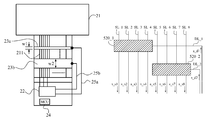
- FIGS. 5 and 6 a schematic view for a one dimensional capacitive touch sensitive device according to a first embodiment of the present invention, and one dimensional capacitive touch panel in FIG. 5 , respectively; this example shows that a one dimensional touch sensitive device includes a one dimensional touch panel 11 , a driving and sensing circuit 12 , an conductive member 13 , and a microcontroller unit 14 .
- the one dimensional touch panel 11 includes plural X electrodes X 1 to X 16 in array form on a substrate (not shown), and material for the substrate may be, not limited to, glass, polycarbonate (PC), PMMA, Polyethylene Terephthalate (PET), or Tri-cellulose Acetate (TCA).
- Each of the electrodes forms a cell of a sensing structure in the panel, and though appears as a square shape in the figure, it is not a limitation, for example, other shape such as rhombus, rectangular, hexagonal, circular or the like may be alternative.
- Each electrode is connected to the driving and sensing circuit 12 through a sensing line 111 .
- two of the electrodes X 3 and X 4 serve for two inputs of a comparator 121 .
- Material for the electrode may be but not limited to Indium Tin Oxide (ITO), Antimony Tin Oxide (ATO), Indium-Zinc Oxide (IZO), Zinc oxide (ZnO) or the like.
- the conductive member 13 in form of bar is laid on a covering layer 151 of an FPC 15 , while at least a portion of each sensing lines 111 is enclosed within the covering layer of the FPC 15 so that the conductive member 13 does not contact with any sensing lines 111 .
- the conductive member 13 is also electrically connected to the driving and sensing circuit 12 through a driving line 16 and crosses sensing lines 111 in orthogonal configuration.
- the driving and sensing circuit 12 and the microcontroller unit 14 are electrically connected to each other, and the microcontroller unit 14 controls the driving and sensing circuit 12 to send signals through the driving line 16 to the conductive member 13 .
- the microcontroller unit 14 controls the driving and sensing circuit 12 to send signals through the driving line 16 to the conductive member 13 .
- Structure of the present invention overcomes a drawback of unstable coupling capacitance in one dimensional touch panel which strongly influences sensing effect.
- a stable coupling capacitance is provided on an FPC in the present invention, and it can be adjusted easily. For example, by adjusting quantity, width, and even voltage of the conductive member, the coupling capacitance can be changed as desired so as to attain the control over stability of coupling capacitance, which is described in detail hereinafter.
- a capacitive touch sensitive device mainly includes a touch panel 21 , a driving and sensing circuit 22 , two conductive members 23 a and 23 b , and a microcontroller unit 24 . Electrodes of the touch panel 21 are connected to the driving and sensing circuit 22 through respective sensing lines 211 .
- the conductive members 23 a and 23 b of the widths W1 and W2 are arranged above the sensing lines 211 and spaced apart from each other.
- the conductive members 23 a and 23 b are also electrically connected to the driving and sensing circuit 22 through driving lines 25 a and 25 b and have a cross and orthogonal relation with respect to the sensing lines 211 .
- the driving and sensing circuit 22 and the microcontroller unit 24 are electrically connected with each other so that the microcontroller unit 24 controls the driving and sensing circuit 22 to drive simultaneously the two conductive members 23 a and 23 b.
- FIG. 8 shows an equivalent circuit diagram for the capacitive touch sensitive device with addition of two conductive members. It shows in the figure that both input terminals V+ and V ⁇ are provided with capacitors in parallel due to addition of the conductive members, and subsequently the equivalent capacitance is increased moderately, leading to a lowered voltage between node A and V+ (also between node A and V ⁇ ). The larger voltage difference occurs to a coupling capacitance C_Finger which is induced by finger touch, and thus the voltage difference between two input terminals V+ and V ⁇ is amplified so that the probing by the driving and sensing circuit 22 becomes more sensitive. It should be noted that both inappropriately large or small equivalent capacitance will result in adverse effect and the best solution can be obtained by adjusting relative area of the conductive members 23 a and 23 b.
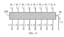
- FIG. 14 illustrates arrangement for a single conductive member and related signal transmission.
- a single conductive member 520 is arranged to cross plural sensing lines SL_ 1 to SL_ 8 , and is electrically connected to a driving and sensing circuit (not shown) via a driving line DL.
- the figure shows that a driving signal is transmitted on the driving line DL, and in response plural sensing signals s_s 1 to s_s 8 are transmitted on the sensing lines SL_ 1 to SL_ 8 .
- FIGS. 15-17 show three kinds of possible arrangement.
- conductive members 520 _ 1 to 520 — q cross the identical group of sensing lines SL_ 1 to SL_ 8 , and are electrically connected to respective driving lines DL_ 1 to DL_q to receive respective driving signals s_d 1 to s_dq, where q is a positive integer, determined by designer.
- the driving signals s_d 1 to s_dq may be the same or different signals as desired, without limitation imposed.
- all conductive members 520 _ 1 to 520 — q may be configured to be electrically connected to the driving and sensing circuit via single driving line, though it is not limitation to the present invention.
- each conductive member can be configured to cross respective groups of sensing lines.
- the respective groups of sensing lines may have no common sensing lines, or alternatively, have at least one common sensing line, and FIG. 16 shows an example of the former.
- each conductive member crossing four sensing lines is taken for example, though the number of four should not be deemed a limitation to the present invention.
- a conductive member 520 _ 1 crosses a group of sensing lines SL_ 1 to SL_ 4 while another conductive member 520 _ 2 crosses another group of sensing lines SL_ 5 to SL_ 8 .
- the conductive members 520 _ 1 and 520 _ 2 are electrically connected with driving lines DL_ 1 and DL_ 2 respectively for receiving respective driving signals s_d 1 and s_d 2 . It can be seen that all sensing lines SL_ 1 to SL_ 4 crossed by the conductive member 520 _ 1 are different from those sensing lines S_ 5 to SL_ 8 crossed by the conductive member 520 _ 2 , that is to say, the respective groups of sensing lines have no common sensing lines. It is apparent that configuration is a typical application of two dimensional capacitive touch panel.
- FIG. 17 shows an example of respective groups of sensing lines having common sensing lines.
- a conductive member 520 _ 1 crosses a group of sensing lines SL_ 1 to SL_ 5 while another conductive member 520 _ 2 crosses another group of sensing lines SL_ 4 to SL_ 8 .
- Two conductive members 520 _ 1 and 520 _ 2 are electrically connected with driving lines DL_ 1 and DL_ 2 respectively for receiving respective driving signals s_d 1 and s_d 2 .
- the sensing lines SL_ 1 to SL_ 5 crossed by the conductive member 520 _ 1 the sensing lines SL_ 4 and SL_ 5 are also crossed by the conductive member 520 _ 2 , that is to say, the respective groups of sensing lines have common sensing lines.
- the number of common lines in the example above should not be deemed a limitation to the present invention.
- driving signals s_d 1 and s_d 2 in examples for FIGS. 16 and 17 can be the same or different signals as desired, and when the driving signals s_d 1 and s_d 2 are of the same, two conductive members 520 _ 1 and 520 _ 2 may be electrically connected to a driving and sensing circuit through a single driving line, though it is not a limitation to the present invention. Further, signal resolution can also be changed by altering the width of the conductive member.
- FIG. 9 arrangement for conductive member of a capacitive touch sensitive device according to a third embodiment of the present invention
- FIG. 10 arrangement for conductive member of a capacitive touch sensitive device according to a fourth embodiment of the present invention
- the conductive member 30 is arranged above sensing lines 32 and on a covering layer of a carrier such as an FFC 31 which encloses the sensing lines 32
- the conductive member 30 is arranged under the sensing lines 32 and directly under the FFC 31 in absence of a covering layer.
- a conductive member 36 is arranged on a covering layer 371 of a PCB 37 and above plural sensing lines 38 .
- FIG. 12 arrangement for conductive member of a capacitive touch sensitive device according to a sixth embodiment of the present invention.
- this example illustrates a conductive member 43 is arranged on one side of a PCB 42 while sensing lines 44 on the opposite side.
- this embodiment primarily provides an conductive member 40 with mesh configuration 41 .
- mesh configuration 41 allows for adjustment of equivalent coupling capacitance and prevention from peeling accident.
- FIG. 18 shows electrodes 50 of the capacitive touch panel are configured to be hexagonal and each of the electrodes is surrounded by six other electrodes, so as to form a honeycomb pattern altogether. Such kind of configuration provides a better recognition resolution for user operation.
- material for conductive member includes but not limited to silver paste, copper, or aluminum foil.
Abstract
Description
Claims (15)
Applications Claiming Priority (3)
| Application Number | Priority Date | Filing Date | Title |
|---|---|---|---|
| TW101134828A | 2012-09-21 | ||
| TW101134828A TWI467458B (en) | 2012-09-21 | 2012-09-21 | Capacitive touch apparatus |
| TW101134828 | 2012-09-21 |
Publications (2)
| Publication Number | Publication Date |
|---|---|
| US20140083834A1 US20140083834A1 (en) | 2014-03-27 |
| US9240782B2 true US9240782B2 (en) | 2016-01-19 |
Family
ID=50315229
Family Applications (1)
| Application Number | Title | Priority Date | Filing Date |
|---|---|---|---|
| US13/854,148 Active 2033-08-25 US9240782B2 (en) | 2012-09-21 | 2013-04-01 | One-dimensional capacitive touch panel with stable coupling capacitance |
Country Status (3)
| Country | Link |
|---|---|
| US (1) | US9240782B2 (en) |
| CN (1) | CN103677467B (en) |
| TW (1) | TWI467458B (en) |
Families Citing this family (6)
| Publication number | Priority date | Publication date | Assignee | Title |
|---|---|---|---|---|
| TWI575444B (en) | 2014-03-12 | 2017-03-21 | 新益先創科技股份有限公司 | Command input device and command input method |
| CN105302346A (en) * | 2014-07-11 | 2016-02-03 | 新益先创科技股份有限公司 | Sensing electrode structure |
| US10409485B2 (en) | 2014-10-09 | 2019-09-10 | Touchplus Information Corp. | Adaptive user input device |
| CN105511141B (en) * | 2015-12-31 | 2019-01-29 | 上海天马微电子有限公司 | A kind of array substrate and touch-control display panel |
| US10579193B2 (en) * | 2017-12-14 | 2020-03-03 | Cypress Semiconductor Corporation | Spatial-frequency-based capacitive motion sensor and method of using the same |
| US10761649B2 (en) | 2018-02-27 | 2020-09-01 | Perfect Shiny Technology (Shenzhen) Limited | Touch input method and handheld apparatus using the method |
Citations (9)
| Publication number | Priority date | Publication date | Assignee | Title |
|---|---|---|---|---|
| US5565658A (en) * | 1992-07-13 | 1996-10-15 | Cirque Corporation | Capacitance-based proximity with interference rejection apparatus and methods |
| US7307626B2 (en) * | 2004-01-27 | 2007-12-11 | Tyco Electronics Corporation | Capacitive touch sensor |
| US7821502B2 (en) * | 2005-07-08 | 2010-10-26 | Atmel Corporation | Two-dimensional position sensor |
| US20110290541A1 (en) * | 2010-05-28 | 2011-12-01 | Shih-Kun Yeh | Flexible flat cable |
| US8228312B2 (en) * | 2007-12-28 | 2012-07-24 | Wacom, Co., Ltd. | Position detecting device |
| US8269744B2 (en) * | 2008-09-05 | 2012-09-18 | Mitsubishi Electric Corporation | Touch screen, touch panel and display device |
| US8514185B2 (en) * | 2006-07-06 | 2013-08-20 | Apple Inc. | Mutual capacitance touch sensing device |
| US8599150B2 (en) * | 2009-10-29 | 2013-12-03 | Atmel Corporation | Touchscreen electrode configuration |
| US8854326B2 (en) * | 2011-03-10 | 2014-10-07 | Wintek Corporation | Touch panel and touch-sensitive display device |
Family Cites Families (3)
| Publication number | Priority date | Publication date | Assignee | Title |
|---|---|---|---|---|
| US7315336B2 (en) * | 2004-06-16 | 2008-01-01 | Tyco Electronics Corporation | Stress seal for touchscreen systems |
| US7692629B2 (en) * | 2006-12-07 | 2010-04-06 | Microsoft Corporation | Operating touch screen interfaces |
| US20120218028A1 (en) * | 2011-02-28 | 2012-08-30 | Tpk Touch Solutions Inc. | Capacitive touch panel, touch sensor structure and a method for manufacturing the capacitive touch panel |
-
2012
- 2012-09-21 TW TW101134828A patent/TWI467458B/en active
-
2013
- 2013-04-01 US US13/854,148 patent/US9240782B2/en active Active
- 2013-09-23 CN CN201310435965.9A patent/CN103677467B/en active Active
Patent Citations (9)
| Publication number | Priority date | Publication date | Assignee | Title |
|---|---|---|---|---|
| US5565658A (en) * | 1992-07-13 | 1996-10-15 | Cirque Corporation | Capacitance-based proximity with interference rejection apparatus and methods |
| US7307626B2 (en) * | 2004-01-27 | 2007-12-11 | Tyco Electronics Corporation | Capacitive touch sensor |
| US7821502B2 (en) * | 2005-07-08 | 2010-10-26 | Atmel Corporation | Two-dimensional position sensor |
| US8514185B2 (en) * | 2006-07-06 | 2013-08-20 | Apple Inc. | Mutual capacitance touch sensing device |
| US8228312B2 (en) * | 2007-12-28 | 2012-07-24 | Wacom, Co., Ltd. | Position detecting device |
| US8269744B2 (en) * | 2008-09-05 | 2012-09-18 | Mitsubishi Electric Corporation | Touch screen, touch panel and display device |
| US8599150B2 (en) * | 2009-10-29 | 2013-12-03 | Atmel Corporation | Touchscreen electrode configuration |
| US20110290541A1 (en) * | 2010-05-28 | 2011-12-01 | Shih-Kun Yeh | Flexible flat cable |
| US8854326B2 (en) * | 2011-03-10 | 2014-10-07 | Wintek Corporation | Touch panel and touch-sensitive display device |
Also Published As
| Publication number | Publication date |
|---|---|
| TWI467458B (en) | 2015-01-01 |
| US20140083834A1 (en) | 2014-03-27 |
| TW201413549A (en) | 2014-04-01 |
| CN103677467B (en) | 2018-05-18 |
| CN103677467A (en) | 2014-03-26 |
Similar Documents
| Publication | Publication Date | Title |
|---|---|---|
| JP6564353B2 (en) | Electrode sheet and touch input device | |
| US9851850B2 (en) | Touch panel and touchscreen device including the same | |
| US9329710B2 (en) | Touchscreen panel and touchscreen device | |
| US10282044B2 (en) | Touch sensing device and display device with a switching unit configured to receive noise from an electrode | |
| US20140168171A1 (en) | Touch sensing device and touch sensing method | |
| US9240782B2 (en) | One-dimensional capacitive touch panel with stable coupling capacitance | |
| JP2008217784A (en) | Touch panel | |
| KR101376887B1 (en) | Touch screen panel and touch screen apparatus | |
| US8970543B2 (en) | Touch sensing apparatus and method thereof | |
| US9146643B2 (en) | Touch sensing apparatus and method thereof | |
| US20140145975A1 (en) | Touchscreen device and screen zoom method thereof | |
| US20140035865A1 (en) | Multi-touch on single layer touch sensor | |
| US8907919B2 (en) | Sensing structure of touch panel | |
| US20140146000A1 (en) | Touch sensing device and touchscreen device | |
| US10572082B2 (en) | Force-touch panel, force-touch sensing device and display system having the same | |
| US20140292708A1 (en) | Touchscreen apparatus | |
| US20140152609A1 (en) | Touch sensing device and touch sensing method | |
| KR20130067564A (en) | Apparatus and method for sensing touch input | |
| US20140139478A1 (en) | Touch sensing method and touch sensing device | |
| KR102183655B1 (en) | Display apparatus | |
| US9417727B2 (en) | Touchscreen device and method of driving the same | |
| KR20140086477A (en) | Apparatus for sensing touch input | |
| US20150153869A1 (en) | Touchscreen device | |
| US10712859B2 (en) | Touch-sensitive control device | |
| US20140168112A1 (en) | Touch sensing method and touch sensing apparatus |
Legal Events
| Date | Code | Title | Description |
|---|---|---|---|
| AS | Assignment |
Owner name: TOUCHPLUS INFORMATION CORP., TAIWAN Free format text: ASSIGNMENT OF ASSIGNORS INTEREST;ASSIGNORS:CHOU, YUNG-CHAN;HU, SHIH HSIEN;REEL/FRAME:030120/0134 Effective date: 20121213 |
|
| FEPP | Fee payment procedure |
Free format text: PAYOR NUMBER ASSIGNED (ORIGINAL EVENT CODE: ASPN); ENTITY STATUS OF PATENT OWNER: SMALL ENTITY |
|
| STCF | Information on status: patent grant |
Free format text: PATENTED CASE |
|
| MAFP | Maintenance fee payment |
Free format text: PAYMENT OF MAINTENANCE FEE, 4TH YR, SMALL ENTITY (ORIGINAL EVENT CODE: M2551); ENTITY STATUS OF PATENT OWNER: SMALL ENTITY Year of fee payment: 4 |
|
| AS | Assignment |
Owner name: DECENTRALIZED MOTION INTELLIGENCE CO., TAIWAN Free format text: CHANGE OF NAME;ASSIGNOR:TOUCHPLUS INFORMATION CORP.;REEL/FRAME:063804/0859 Effective date: 20211001 |
|
| MAFP | Maintenance fee payment |
Free format text: PAYMENT OF MAINTENANCE FEE, 8TH YR, SMALL ENTITY (ORIGINAL EVENT CODE: M2552); ENTITY STATUS OF PATENT OWNER: SMALL ENTITY Year of fee payment: 8 |