BACKGROUND
I. Field
The present disclosure relates generally to electronics, and more specifically to techniques for supporting wireless communication.
II. Background
A wireless device (e.g., a cellular phone or a smartphone) may transmit and receive data for two-way communication with a wireless communication system. The wireless device may include a transmitter for data transmission and a receiver for data reception. For data transmission, the transmitter may modulate a transmit local oscillator (LO) signal with data to obtain a modulated radio frequency (RF) signal, amplify the modulated RF signal to obtain an output RF signal having the proper transmit power level, and transmit the output RF signal via an antenna to a base station. For data reception, the receiver may obtain a received RF signal via the antenna, amplify and downconvert the received RF signal with a receive LO signal, and process the downconverted signal to recover data sent by the base station.
A wireless device may support communication with multiple wireless systems of different radio access technologies (RATs). Each wireless system may have certain characteristics and requirements. It is desirable to efficiently support concurrent communication with wireless systems of different RATs.
SUMMARY
A wireless device supporting concurrent communication with multiple wireless systems of different RATs is disclosed herein. In an exemplary design, an apparatus (e.g., a wireless device or an integrated circuit (IC)) may include first and second receivers supporting concurrent signal reception from wireless systems of different RATs. The first receiver may receive a first downlink signal from a first wireless system of a first RAT. The second receiver may receive a second downlink signal from a second wireless system of a second RAT that is different from the first RAT. The first and second receivers may operate concurrently. The second receiver may (i) be broadband and support a plurality of frequency band and/or (ii) support carrier aggregation.
In an exemplary design, the first receiver may comprise a plurality of low-noise amplifiers (LNAs) for a plurality of bands. Each LNA may cover at least one of the plurality of bands. The second receiver may comprise a single LNA for the plurality of bands. In another exemplary design, the first receiver may comprise a first plurality of LNAs for a plurality of bands. The second receiver may comprise a second plurality of LNAs for the plurality of bands. In an exemplary design, the first and second receivers may concurrently receive downlink signals on first and second sets of carriers, respectively, for carrier aggregation.
The apparatus may further include first and second LO generators. The first LO generator may generate a first LO signal for the first receiver based on a first divider ratio. The second LO generator may generate a second LO signal for the second receiver based on a second divider ratio, which may be different from the first divider ratio. The first LO generator may include a first voltage controlled oscillator (VCO) operating at a first frequency. The second LO generator may include a second VCO operating at a second frequency. The first and second divider ratios may be selected to obtain at least a predetermined amount of separation between the first and second frequencies in order to mitigate VCO pulling.
The apparatus may further include first and second transmitters. The first transmitter may transmit a first uplink signal to the first wireless system of the first RAT. The second transmitter may transmit a second uplink signal to the second wireless system of the second RAT. The second transmitter may be broadband and/or may support carrier aggregation.
Various aspects and features of the disclosure are described in further detail below.
BRIEF DESCRIPTION OF THE DRAWINGS
FIG. 1 shows a wireless device communicating with multiple wireless systems of different RATs.
FIGS. 2 to 4 show three exemplary designs of the wireless device in FIG. 1.
FIGS. 5 to 7 show exemplary designs of transceivers within the wireless device in FIGS. 2 to 4, respectively.
FIG. 8 shows a process for supporting wireless communication.
DETAILED DESCRIPTION
The detailed description set forth below is intended as a description of exemplary designs of the present disclosure and is not intended to represent the only designs in which the present disclosure can be practiced. The term “exemplary” is used herein to mean “serving as an example, instance, or illustration.” Any design described herein as “exemplary” is not necessarily to be construed as preferred or advantageous over other designs. The detailed description includes specific details for the purpose of providing a thorough understanding of the exemplary designs of the present disclosure. It will be apparent to those skilled in the art that the exemplary designs described herein may be practiced without these specific details. In some instances, well-known structures and devices are shown in block diagram form in order to avoid obscuring the novelty of the exemplary designs presented herein.
FIG. 1 shows a wireless device 110 capable of communicating with multiple wireless communication systems of different RATs, which may include a first wireless system 120 of a first RAT and a second wireless system 122 of a second RAT. Wireless systems 120 and 122 may each be a Code Division Multiple Access (CDMA) system, a Global System for Mobile Communications (GSM) system, a Long Term Evolution (LTE) system, a wireless local area network (WLAN) system, or some other wireless system. A CDMA system may implement a RAT such as Wideband CDMA (WCDMA), CDMA 1× or cdma2000, Time Division Synchronous Code Division Multiple Access (TD-SCDMA), etc. For example, wireless system 120 may be a GSM system, and wireless system 122 may be a WCDMA system. As another example, wireless system 120 may be an LTE system, and wireless system 122 may be a CDMA system.
For simplicity, FIG. 1 shows wireless system 120 including one base station 130 and one system controller 140, and wireless system 122 including one base station 132 and one system controller 142. In general, each wireless system may include any number of base stations and any set of network entities. Each base station may support communication for wireless devices within its coverage.
Wireless device 110 may also be referred to as a user equipment (UE), a mobile station, a terminal, an access terminal, a subscriber unit, a station, etc. Wireless device 110 may be a cellular phone, a smartphone, a tablet, a wireless modem, a personal digital assistant (PDA), a handheld device, a laptop computer, a smartbook, a netbook, a cordless phone, a wireless local loop (WLL) station, a Bluetooth device, etc. Wireless device 110 may be capable of communicating with wireless system 120 and/or 122. Wireless device 110 may also be capable of receiving signals from broadcast stations (e.g., a broadcast station 134), satellites (e.g., a satellite 150) in one or more global navigation satellite systems (GNSS), etc. Wireless device 110 may support one or more RATs for wireless communication such as GSM, WCDMA, cdma2000, LTE, 802.11, etc. The terms “radio access technology”, “RAT”, “radio technology”, “air interface”, and “standard” are often used interchangeably.
FIG. 2 shows a block diagram of a wireless device 110 a, which is one exemplary design of wireless device 110 in FIG. 1. In this design, wireless device 110 a includes a primary antenna 210, a secondary antenna 212, a transceiver 220 a, and a data processor/controller 280. Transceiver 220 a supports signal reception from both antennas 210 and 212 for a first RAT, signal reception from antenna 210 for a second RAT, and signal transmission via antenna 210 for both the first and second RATs. Transceiver 220 a also supports concurrent communication with both the first and second RATs.
In the design shown in FIG. 2, transceiver 220 a includes an antenna interface circuit 222, a multi-band receiver 230 a for a first RAT for primary antenna 210, a multi-band receiver 230 b for the first RAT for secondary antenna 212, a multi-band transmitter 240 a for the first RAT, a broadband receiver 230 z for a second RAT, and a broadband transmitter 240 z for the second RAT. A multi-band receiver or a multi-band transmitter may support multiple frequency bands (or simply, “bands”) and may include circuits designed for meet applicable requirements for each supported band. For example, a multi-band receiver may include multiple low noise amplifiers (LNAs), with each LNA supporting one or more bands. A multi-band transmitter may include multiple power amplifiers (PAs), with each PA supporting one or more bands. Each PA may be a single-stage amplifier or a multi-stage amplifier and may have a fixed gain or a variable gain. A multi-stage amplifier may include an inter-stage filter or no inter-stage filter and may have inter-stage matching or no inter-stage matching. A portion of a multi-stage amplifier may be located off-chip, e.g., within an antenna interface circuit. A broadband receiver or a broadband transmitter may support multiple bands, may include circuits designed to provide good performance for all supported bands, and may have a reduced number of input and/or output ports. For example, a broadband receiver may include a single broadband/wideband LNA for all supported bands and may have a reduced number of input ports (e.g., one input port) in order to reduce pin count and save chip area on an IC chip. A multi-band transmitter may include a single broadband/wideband PA for all supported bands and may have a reduced number of output ports (e.g., one output port) in order to reduce pin count and save chip area on an IC chip. A broadband receiver or a transmitter broadband may interface with a tunable or switchable front-end circuit, which may further interface with an antenna interface circuit. Broadband performance may be achieved with or without single-pole-multiple-throw switches.
In the design shown in FIG. 2, transceiver 220 a includes an LO generator 250 for receivers 230 a and 230 b for the first RAT, an LO generator 260 for transmitter 240 a for the first RAT, and an LO generator 270 for receiver 230 z and transmitter 240 z for the second RAT. LO generator 250 generates receive LO signals for receivers 230 a and 230 b. In the design shown in FIG. 2, LO generator 250 includes a frequency synthesizer 252 and a divider 258. Frequency synthesizer 252 generates a first oscillator signal at a first frequency. Divider 258 divides the first oscillator signal in frequency by a factor of RX_N1 to generate receive LO signals at a target RX frequency for receivers 230 a and 230 b. RX_N1 is a frequency divider ratio for receivers 230 a and 230 b.
LO generator 260 generates a transmit LO signal for transmitter 240 a. LO generator 260 includes a frequency synthesizer 262 and a divider 268. Frequency synthesizer 262 generates a second oscillator signal at a second frequency. Divider 268 divides the second oscillator signal in frequency by a factor of TX_N1 to generate the transmit LO signal at a target TX frequency for transmitter 240 a.
LO generator 270 generates receive and transmit LO signals for receiver 230 z and transmitter 240 z. LO generator 270 includes a frequency synthesizer 272 and dividers 278 and 279. Frequency synthesizer 272 generates a third oscillator signal at a third frequency. Divider 278 divides the third oscillator signal in frequency by a factor of RX_N2 to generate a receive LO signal at a target RX frequency for receiver 230 z. Divider 279 divides the third oscillator signal in frequency by a factor of TX_N2 to generate a transmit LO signal at a target TX frequency for transmitter 240 z.
Data processor/controller 280 may perform various functions for wireless device 110 a. For example, data processor 210 may perform processing for data received via receivers 230 and processing for data transmitted via transmitters 240. Controller 280 may control the operation of various circuits within receivers 230 and transmitters 240. A memory 282 may store program codes and data for data processor/controller 280. Memory 282 may be internal to data processor/controller 280 (as shown in FIG. 2) or external to data processor/controller 280 (not shown in FIG. 2). An LO controller 284 may control the operation of LO generators 250, 260 and 270. For example, LO controller 284 may select a suitable divider ratio for each LO signal being generated, so that good performance can be obtained, as described below. Data processor/controller 280 may be implemented on one or more application specific integrated circuits (ASICs) and/or other ICs.
Receivers 230 a and 230 z may operate concurrently to receive downlink signals from two wireless systems of different RATs. Receiver 230 a may receive downlink signals from a first wireless system of a first RAT, e.g., WCDMA. Receiver 230 z may concurrently receive downlink signals from a second wireless system of a second RAT, e.g., GSM. For example, receiver 230 a may support bi-directional communication with the first wireless system, and receiver 230 z may support monitoring and/or measurement of the second wireless system for inter-RAT (IRAT) operation.
Transmitters 240 a and 240 z may operate to transmit uplink signals to one or more wireless systems. Transmitter 240 a may transmit a first uplink signal to the first wireless system of the first RAT. Transmitter 240 z may concurrently transmit a second uplink signal to the second wireless system of the second RAT. For example, transmitter 240 a may support communication with the first wireless system, and transmitter 240 z may support reporting of feedback information (e.g., received signal strength) to the second wireless system.
In general, any combination of receivers 230 and transmitters 240 may be active at any given moment. For example, receivers 230 a and 230 z may be active concurrently to receive downlink signals from two wireless systems of different RATs. Transmitters 240 a and 240 z may be active concurrently to transmit uplink signals to two wireless systems of different RATs. One or more receivers 230 and one or more transmitters 240 may also be active concurrently to receive downlink signals and transmit uplink signals to multiple wireless systems of different RATs.
Receivers 230 a, 230 b and 230 z may each support one or more RATs. The LO generator for each receiver 230 may be designed to meet applicable requirements for each RAT supported by that receiver. For example, receiver 230 a may support GSM, and LO generator 250 may be required to achieve (i) −35 dBc integrated phase noise (IPN) from 100 Hertz (Hz) to 100 kiloHertz (KHz) and (ii) −118 dBc phase noise at 400 KHz offset. Alternatively or additionally, receiver 230 a may support LTE, and LO generator 250 may be required to achieve −38 dBc IPN from 5 KHz to 9 megaHertz (MHz).
LO generator 250 may support multiple RATs and may have one or more configurable parameters in order to meet applicable requirements for each supported RAT. The configurable parameter(s) may include configurable loop bandwidth, loop filter, VCO gain (Kvco), charge pump, reference clock, etc. Each configurable parameter may have multiple possible settings. A suitable setting may be selected for each configurable parameter based on the requirements of the RAT being supported. In one design, a look-up table may implement a two-dimensional table having columns for configurable parameters and rows for supported RATs. An entry in column x and row y may store a parameter value to use for a configurable parameter corresponding to column x for a RAT corresponding to row y. The look-up table may be accessed with a RAT with which communication is established or desired. Parameter values from entries in the row corresponding to the RAT may be retrieved and applied to LO generator 250.
In general, each LO generator may support one or more RATs. Each LO generator may have fixed parameters and/or configurable parameters. Each configurable parameter may be set to a suitable value based on the requirements of a RAT with which communication is established or desired.
LO controller 284 within data processor/controller 280 may receive information indicative of (i) which receivers 230 (if any) and which transmitters 240 (if any) are active and (ii) an RX frequency of each active receiver 230 and a TX frequency of each active transmitter 240. LO controller 284 may determine a divider ratio for each LO generator for each active receiver or transmitter such that (i) an LO signal at a target frequency is provided to each active receiver or transmitter and (ii) VCOs for all active receivers and transmitters do not operate too close in frequency in order to mitigate VCO pulling. Two VCOs may be considered to be too close in frequency if their operating frequencies are within a predetermined threshold, i.e., if the absolute difference between the VCO operating frequencies is less than the predetermined threshold. For example, if RX and/or TX frequencies for active receivers and/or transmitters are too close in frequency, then LO controller 284 may select different divider ratios for the VCOs for the active receivers and/or transmitters so that the operating frequencies of the VCOs are not too close to each other. LO controller 284 may dynamically determine divider ratios for the active receivers and/or transmitters, e.g., whenever there is a change in frequency or a change in active receiver or transmitter. This may provide good performance for simultaneous reception and/or transmission from/to multiple wireless systems of different RATs.
Wireless device 110 may support carrier aggregation, which is operation on multiple carriers. Carrier aggregation may also be referred to as multi-carrier operation. A carrier may refer to a range of frequencies used for communication and may be associated with certain characteristics. For example, a carrier may be associated with system information and/or control information describing operation on the carrier. A carrier may also be referred to as a component carrier (CC), a frequency channel, a cell, etc. A band may include one or more carriers. Each carrier may cover up to 20 MHz in LTE. Wireless device 110 may be configured with up to 5 carriers in one or two bands in LTE Release 11.
Wireless device 110 may include multiple receivers to concurrently receive multiple downlink signals at different frequencies. These multiple downlink signals may be sent by one or more base stations on multiple carriers at different frequencies for carrier aggregation. Each receiver may receive one or more downlink signals sent on one or more carriers to wireless device 110.
FIG. 3 shows a block diagram of a wireless device 110 b, which is another exemplary design of wireless device 110 in FIG. 1. In this design, wireless device 110 b includes antennas 210 and 212, a transceiver 220 b, and data processor/controller 280. Transceiver 220 b includes antenna interface circuit 222, multi-band receivers 330 a and 330 b for a first carrier set for antennas 210 and 212, respectively, multi-band receivers 330 c and 330 d for a second carrier set for antennas 210 and 212, respectively, a multi-band transmitter 340 a for a first RAT, and a broadband transmitter 340 z for a second RAT.
Transceiver 220 b further includes an LO generator 350 for receivers 330 a and 330 b, an LO generator 360 for transmitter 340 a, and an LO generator 370 for receivers 330 c and 330 d and transmitter 340 z. LO generator 350 generates receive LO signals for receivers 330 a and 330 b and includes a frequency synthesizer 352 and a divider 358. LO generator 360 generates a transmit LO signal for transmitter 340 a and includes a frequency synthesizer 362 and a divider 368. LO generator 370 generates receive LO signals for receivers 330 a and 330 b and a transmit LO signal for transmitter 340 z. LO generator 370 includes a frequency synthesizer 372 and dividers 378 and 379.
Receiver 330 a and 330 b may be used to receive downlink signals on a first set of carriers via antennas 210 and 212, respectively. Receiver 330 c and 330 d may be used to receive downlink signals on a second set of carriers via antennas 210 and 212, respectively. Receivers 330 a, 330 b, 330 c and 330 d may be designed to meet applicable requirements for signal reception with carrier aggregation. Transmitter 340 a may be designed to meet applicable requirements for signal transmission. Transmitter 340 z may be a broadband transmitter supporting multiple bands.
Receivers 330 a and 330 c may operate concurrently to receive downlink signals on multiple sets of carriers for carrier aggregation. Receivers 330 a and 330 c may also operate concurrently to receive downlink signals from two wireless systems of different RATs for inter-RAT operation. Receiver 330 a may receive downlink signals from a first wireless system of a first RAT, e.g., LTE. Receiver 330 c may concurrently receive downlink signals from a second wireless system of a second RAT, e.g., GSM. For example, receiver 330 a may support communication with the first wireless system, and receiver 330 c may support monitoring and/or measurement of the second wireless system for inter-RAT operation.
Transmitters 340 a and/or 340 z may operate to transmit uplink signals to one or more wireless systems. Transmitter 340 a may transmit a first uplink signal to the first wireless system of the first RAT. Transmitter 340 z may concurrently transmit a second uplink signal to the second wireless system of the second RAT. For example, transmitter 340 a may support communication with the first wireless system, and transmitter 340 z may support reporting of feedback information (e.g., received signal strength) to the second wireless system.
In general, any combination of receivers and transmitters may be active at any given moment. For example, receivers 330 a and 330 c may be active concurrently to receive downlink signals from two wireless systems of different RATs. Transmitters 340 a and 340 z may be active concurrently to transmit uplink signals to two wireless systems of different RATs. One or more receivers 330 and one or more transmitters 340 may also be active concurrently to receive downlink signals and transmit uplink signals to multiple wireless systems of different RATs.
FIG. 4 shows a block diagram of a wireless device 110 c, which is yet another exemplary design of wireless device 110 in FIG. 1. In this design, wireless device 110 c includes antennas 210 and 212, a transceiver 220 c, and data processor/controller 280. Transceiver 220 c includes antenna interface circuit 222, multi-band receivers 330 a, 330 b, 330 c and 330 d and transmitter 340 a, which are part of transceiver 220 b in FIG. 3. Transceiver 220 c also includes a multi-band transmitter 340 b for the second carrier set.
Transceiver 220 c further includes an LO generator 350 a for receivers 330 a and 330 b, an LO generator 350 b for receivers 330 c and 330 d, an LO generator 360 a for transmitter 340 a, and an LO generator 360 b for transmitter 340 b. LO generator 350 a generates receive LO signals for receivers 330 a and 330 b and includes a frequency synthesizer 352 a and a divider 358 a. LO generator 350 b generates receive LO signals for receivers 330 c and 330 d and includes a frequency synthesizer 352 b and a divider 358 b. LO generator 360 a generates a transmit LO signal for transmitter 340 a and includes a frequency synthesizer 362 a and a divider 368 a. LO generator 360 b generates a transmit LO signal for transmitter 340 b and includes a frequency synthesizer 362 b and a divider 368 b.
Receivers 330 a and 330 b may be used to receive downlink signals on a first set of carriers via antennas 210 and 212, respectively. Receivers 330 c and 330 d may be used to receive downlink signals on a second set of carriers via antennas 210 and 212, respectively. Receivers 330 a, 330 b, 330 c and 330 d may be designed to meet applicable requirements for signal reception with carrier aggregation.
Transmitter 340 a may be used to transmit uplink signals on the first set of carriers via antenna 210 and/or 212. Transmitter 340 b may be used to transmit uplink signals on the second set of carriers via antenna 210 and/or 212. Transmitters 340 a and 340 b may be designed to meet applicable requirements for signal transmission with carrier aggregation.
Receivers 330 a and 330 c may operate concurrently to receive downlink signals on multiple sets of carriers for carrier aggregation. Receivers 330 a and 330 c may also operate concurrently to receive downlink signals from two wireless systems of different RATs for inter-RAT operation. Receiver 330 a may receive downlink signals from a first wireless system of a first RAT, e.g., LTE. Receiver 330 c may concurrently receive downlink signals from a second wireless system of a second RAT, e.g., GSM. For example, receiver 330 a may support communication with the first wireless system, and receiver 330 c may support monitoring and/or measurement of the second wireless system for inter-RAT operation.
Transmitters 340 a and 340 b may operate concurrently to transmit uplink signals on multiple sets of carriers for carrier aggregation. Transmitters 340 a and 340 b may also operate concurrently to transmit uplink signals to two wireless systems of different RATs for inter-RAT operation. Transmitter 340 a may transmit a first uplink signal to the first wireless system of the first RAT. Transmitter 340 b may concurrently transmit a second uplink signal to the second wireless system of the second RAT. For example, transmitter 340 a may support communication with the first wireless system, and transmitter 340 b may support reporting of feedback information (e.g., received signal strength) to the second wireless system.
In general, any combination of receivers and transmitters may be active at any given moment. For example, receivers 330 a and 330 c may be active concurrently to receive downlink signals from two wireless systems of different RATs. Transmitters 340 a and 340 b may be active concurrently to transmit uplink signals to two wireless systems of different RATs. One or more receivers 330 and one or more transmitters 340 may also be active concurrently to receive downlink signals and transmit uplink signals to multiple wireless systems of different RATs.
The receivers and transmitters in FIGS. 2 to 4 may be implemented in various manners. A transmitter or a receiver may be implemented with a super-heterodyne architecture or a direct-conversion architecture. In the super-heterodyne architecture, a signal is frequency converted between RF and baseband in multiple stages, e.g., from RF to an intermediate frequency (IF) in one stage, and then from IF to baseband in another stage for a receiver. In the direct-conversion architecture, which is also referred to as a zero-IF architecture, a signal is frequency converted between RF and baseband in one stage. The super-heterodyne and direct-conversion architectures may use different circuit blocks and/or have different requirements. Some exemplary designs of receivers and transmitters implemented with the direct-conversion architecture are described below.
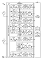
FIG. 5 shows a block diagram of a wireless device 110 x, which is one exemplary design of wireless device 110 a in FIG. 2. In the design shown in FIG. 5, multi-band receiver 230 a includes multiple (K) LNAs 232 aa to 232 ak, a downconverter 234 a, a lowpass filter (LPF) 236 a, and an amplifier (Amp) 238 a. LNAs 232 aa to 232 ak have their inputs coupled to primary antenna 210 via antenna interface circuit 222 and their outputs coupled to downconverter 234 a. Downconverter 234 a has its output coupled to lowpass filter 236 a, which has its output coupled to amplifier 238 a. Multi-band receiver 230 b includes multiple (K) LNAs 232 ba to 232 bk, a downconverter 234 b, a lowpass filter 236 b, and an amplifier 238 b, which are coupled in similar manner as LNAs 232 aa to 232 ak, downconverter 234 a, lowpass filter 236 a, and amplifier 238 a in receiver 230 a. Broadband receiver 230 z includes an LNA 232 z, a downconverter 234 z, a lowpass filter 236 z, and an amplifier 238 z, which are coupled as shown in FIG. 5.
In the design shown in FIG. 5, multi-band transmitter 240 a includes an amplifier (Amp) 242 a, a lowpass filter 244 a, an upconverter 246 a, and multiple (K) power amplifiers (PAs) 248 aa to 248 ak. Amplifier 242 a has its input coupled to data processor 280 and its output coupled to lowpass filter 244 a. Lowpass filter 244 a has its output coupled to upconverter 246 a. PAs 248 aa to 248 ak have their inputs coupled to upconverter 246 a and their outputs coupled to antenna 210 via antenna interface circuit 222. Broadband transmitter 240 z includes an amplifier 242 z, a lowpass filter 244 z, an upconverter 246 z, and a PA 248 z, which are coupled as shown in FIG. 5. PA 248 z may be coupled to primary antenna 210 or secondary antenna 212 via antenna interface circuit 222.
FIG. 5 shows an exemplary design of receivers 230 a, 230 b and 230 z. In general, a receiver may include any set of circuits to process a received RF signal. For example, a receiver may include one or more amplifiers, filters, downconverters, etc. FIG. 5 also shows an exemplary design of transmitters 240 a and 240 z. In general, a transmitter may include any set of circuits to generate an output RF signal. For example, a transmitter may include one or more amplifiers, filters, upconverters, etc.
The circuits in a receiver or a transmitter may be arranged differently from the configuration shown in FIG. 5. For example, a receiver may include an amplifier between a downconverter and a lowpass filter. A transmitter may include an amplifier between a lowpass filter and an upconverter. Other circuits not shown in FIG. 5 may also be used to condition the signals in a transmitter or a receiver. For example, matching circuits may be located at an output of a PA and/or at an input of an LNA. Some circuits in FIG. 5 may also be omitted. All or a portion of transceiver 220 x may be implemented on one or more analog integrated circuits (ICs), RF ICs (RFICs), mixed-signal ICs, etc.
Wireless device 110 x may support reception of downlink signals from one or more wireless systems via primary antenna 210 and/or secondary antenna 212. Wireless device 110 x may also support transmission of uplink signals to one or more wireless systems via primary antenna 210 and/or secondary antenna 212.
For signal reception via primary antenna 210, signals transmitted by base stations and/or other transmitter stations may be received by antenna 210, which may provide a primary received RF signal. Antenna interface circuit 222 may filter and route the primary received RF signal to a selected receiver 230 a or 230 z. Antenna interface circuit 222 may include one or more switches, duplexers, diplexers, transmit filters, receive filters, matching circuits, directional couplers, etc. If receiver 230 a is the selected receiver, then the primary received RF signal may be amplified by a selected LNA among the K LNAs 232 aa to 232 ak. Downconverter 234 a may downconvert the amplified RF signal from the selected LNA with a receive LO signal from LO generator 250 and provide a downconverted signal. The downconverted signal may be filtered by lowpass filter 236 a and amplified by amplifier 238 a to obtain a baseband input signal, which may be provided to data processor 280. If receiver 230 z is the selected receiver, then the primary received RF signal may be amplified by LNA 232 z, downconverted by downconverter 234 z, filtered by lowpass filter 236 z, and amplified by amplifier 238 z to obtain a baseband input signal, which may be provided to data processor 280.
For signal reception via secondary antenna 212, signals transmitted by base stations and/or other transmitter stations may be received by antenna 212, which may provide a secondary received RF signal to receiver 230 b via antenna interface circuit 222. The secondary received RF signal may be amplified by one of LNAs 232 ba to 232 bk, downconverted by downconverter 234 b, filtered by lowpass filter 236 b, and amplified by amplifier 238 b to obtain a baseband input signal, which may be provided to data processor 280.
For signal transmission, data processor 280 may process data to be transmitted and provide a first output baseband signal to transmitter 240 a. Within transmitter 240 a, the first output baseband signal may be amplified by amplifier 242 a, filtered by lowpass filter 244 a, upconverted by upconverter 246 a, and amplified by one of PAs 248 aa to 248 ak to obtain a first output RF signal. The first output RF signal may be routed through antenna interface circuit 222 and transmitted via antenna 210 and/or 212. Alternatively or additionally, data processor 280 may provide a second output baseband signal to transmitter 240 z. Within transmitter 240 z, the second output baseband signal may be amplified by amplifier 242 z, filtered by lowpass filter 244 z, upconverted by upconverter 246 z, and amplified by PA 248 z to obtain a second output RF signal, which may be routed through antenna interface circuit 222 and transmitted via antenna 212.
LO generator 250 generates receive LO signals for receivers 230 a and 230 b. In the design shown in FIG. 5, LO generator 250 includes frequency synthesizer 252 and divider 258, and frequency synthesizer 252 includes a phase locked loop (PLL) 254 and a VCO 256. VCO 256 generates a first oscillator signal at a first frequency, which is determined by a first control signal from PLL 254. PLL 254 receives a reference signal and the first oscillator signal, compares the phase of the first oscillator signal against the phase of the reference signal, and generates the first control signal for VCO 256 such that the phase of the first oscillator signal is locked to the phase of the reference signal. Divider 258 divides the first oscillator signal in frequency by a factor of RX_N1 to generate receive LO signals at a target RX frequency for downconverters 234 a and 234 b in receivers 230 a and 230 b.
LO generator 260 generates a transmit LO signal for transmitter 240 a. LO generator 260 includes frequency synthesizer 262 and a divider 268, and frequency synthesizer 262 includes a PLL 264 and a VCO 266. Frequency synthesizer 262 generates a second oscillator signal at a second frequency. Divider 268 divides the second oscillator signal in frequency by a factor of TX_N1 to generate the transmit LO signal at a target TX frequency for upconverter 246 a in transmitter 240 a.
LO generator 270 generates receive and transmit LO signals for receiver 230 z and transmitter 240 z. LO generator 270 includes frequency synthesizer 272 and dividers 278 and 279, and frequency synthesizer 272 includes a PLL 274 and a VCO 276. Frequency synthesizer 272 generates a third oscillator signal at a third frequency. Divider 278 divides the third oscillator signal in frequency by a factor of RX_N2 to generate a receive LO signal at a target RX frequency for downconverter 234 z within receiver 230 z. Divider 279 divides the third oscillator signal in frequency by a factor of TX_N2 to generate a transmit LO signal at a target TX frequency for upconverter 246 z within transmitter 240 z.
In the design shown in FIG. 5, multi-band receiver 230 a includes multiple LNAs 232 aa to 232 ak to support multiple bands. Each LNA 232 may support one or more bands and may be coupled to a separate matching circuit (e.g., within antenna interface circuit 222) for the one or more bands covered by that LNA. The multiple LNAs 232 aa to 232 ak may allow receiver 230 a to meet applicable requirements, e.g., for linearity, dynamic range, noise figure, etc. These requirements may be dependent on one or more RATs supported by receiver 230 a.
Broadband receiver 230 z may support multiple bands using broadband circuits. For example, receiver 230 z may include a single broadband LNA 232 z that can support multiple bands. LNA 232 z may have a different circuit design than LNAs 232 aa to 232 ak. For example, LNA 232 z may be implemented with a common-gate LNA having its source receiving a received RF signal and its gate coupled to alternating current (AC) ground. In contrast, LNAs 232 aa to 232 ak may each be implemented with a common-source LNA having its gate receiving a received RF signal and its source coupled to circuit ground or a source degeneration inductor. Other circuits in broadband receiver 230 z may also be designed to support broadband operation. For example, downconverter 234 z may be designed to operate at multiple bands. Lowpass filter 236 z may be designed with a configurable bandwidth.
In the design shown in FIG. 5, multi-band transmitter 240 a includes multiple PAs 248 aa to 248 ak to support multiple bands. Each PA 248 may support one or more bands and may be coupled to a separate matching circuit (e.g., within antenna interface circuit 222) for the one or more bands covered by that PA. The multiple PAs 248 aa to 248 ak may allow transmitter 240 a to meet applicable requirements, e.g., for linearity, dynamic range, output power, etc. These requirements may be dependent on one or more RATs supported by transmitter 240 a.
Broadband transmitter 240 z may support multiple bands using broadband circuits. For example, transmitter 240 z may include a single broadband PA 248 z that can support multiple bands. PA 248 z may have a different circuit design than PAs 248 aa to 248 ak.
In the designs shown in FIGS. 2 and 5, receiver 230 z and transmitter 240 z may be broadband in order to save IC chip area and cost. Receiver 230 z and transmitter 240 z may also be multi-mode and may support all RATs supported by receiver 230 a and transmitter 240 a. Receiver 230 z and transmitter 240 z may share one LO generator 270 in order to save IC chip area. The operation of receiver 230 a and transmitter 240 a may be negligibly affected when receiver 230 z and transmitter 240 z are turned ON or OFF.
Multiple VCOs 256 and 276 within frequency synthesizers 252 and 272 may be used to generate receive LO signals to support concurrent reception of downlink signals from multiple wireless systems of different RATs. LO generators 250 and 270 may be configured to support concurrent signal reception for multiple RATs. For example, receivers 230 a and 230 z may concurrently receive downlink signals from WCDMA and GSM systems, respectively, in UMTS Band 8 (B8). A first RX frequency (or RX1 frequency) for receiver 230 a for the WCDMA system may be close or far from a second RX frequency (or RX2 frequency) for receiver 230 z for the GSM system. If the RX1 frequency is close to the RX2 frequency (e.g., separated by 0.1 MHz or less) and if the same divider ratio (e.g., RX— N1=RX— N2) is used for both dividers 258 and 278, then VCOs 256 and 276 may operate at close frequencies and may pull each other. Frequency synthesizers 252 and 272 may then have degraded phase noise and spurious performance due to VCO pulling.
In an exemplary design, different divider ratios may be used for LO generators for multiple receivers operating concurrently. In the example described above, different divider ratios (RX— N1≠ RX— N2) may be used for dividers 258 and 278 in LO generators 250 and 270 in order to mitigate VCO pulling. The divider ratios RX_N1 and RX_N2 may be selected such that the operating frequency of VCO 256 is sufficiently far from the operating frequency of VCO 276 in order to mitigate VCO pulling.
In an exemplary design, different divider ratios may be used for LO generators for multiple transmitters operating concurrently. For example, different divider ratios TX_N1 and TX_N2 may be used for dividers 268 and 279 in LO generators 260 and 270 in order to mitigate VCO pulling. The divider ratios TX_N1 and TX_N2 may be selected such that the operating frequency of VCO 256 is sufficiently far from the operating frequency of VCO 276 in order to mitigate VCO pulling.
In an exemplary design, different divider ratios may be used for LO generators for a receiver and a transmitter operating concurrently. In one operating scenario, receivers 230 a and 230 z and transmitter 240 a may operate concurrently. Receiver 230 a and transmitter 240 a may support communication with a first wireless system of a first RAT. Receiver 230 z may support signal reception from a second wireless system of a second RAT. Divider ratio RX_N2 for divider 278 and divider ratio TX_N1 for divider 268 may be selected such that (i) a transmit LO signal at a desired TX frequency is obtained for transmitter 240 a, (ii) a receive LO signal at a desired RX frequency is obtained for receiver 230 z, and (iii) the frequency of VCO 266 for transmitter 240 b is not too close to the frequency of VCO 276 for receiver 230 z in order to mitigate VCO pulling.
In another operating scenario, receivers 230 a and 230 z and transmitters 240 a and 240 z may operate concurrently. Receiver 230 a and transmitter 240 a may support communication with a first wireless system of a first RAT. Receiver 230 z and transmitter 240 z may support communication with a second wireless system of a second RAT. Divider ratio RX_N1 for divider 258, divider ratio TX_N1 for divider 268, divider ratio RX_N2 for divider 278, and divider ratio TX_N2 for divider 279 may be selected such that (i) transmit LO signals at desired TX frequencies are obtained for transmitters 240 a and 240 z, (ii) receive LO signals at desired RX frequencies are obtained for receivers 230 a and 230 z, and (iii) the frequencies of VCOs 256, 266 and 276 are not too close together in order to mitigate VCO pulling.
Receiver 230 z and transmitter 240 z may be active concurrently to monitor and/or measure downlink signals from the second wireless system and report feedback information to the second wireless system. If the second wireless system utilizes time division duplexing (TDD), then the RX frequency for the second wireless system is equal to the TX frequency for the second wireless system, and one LO generator 270 may be used to generate both the receive LO signal for receiver 230 z and the transmit LO signal for transmitter 240 z. LO generator 270 may operate in a time division multiplexed manner and may generate the receive LO signal during receive time intervals or the transmit LO signal during transmit time intervals. In this case, VCO pulling would not be encountered by LO generator 270.
FIG. 6 shows a block diagram of a wireless device 110 y, which is an exemplary design of wireless device 110 b in FIG. 3. In this design, multi-band receiver 330 a includes multiple (K) LNAs 332 aa to 332 ak, a downconverter 334 a, a lowpass filter 336 a, and an amplifier 338 a, which are coupled as shown in FIG. 6. Multi-band receivers 330 b, 330 c and 330 d may each be implemented in similar manner as multi-band receiver 330 a. Multi-band transmitter 340 a includes an amplifier 342 a, a lowpass filter 344 a, an upconverter 346 a, and multiple (K) PAs 348 aa to 348 ak, which are coupled as shown in FIG. 6. Broadband transmitter 340 z includes an amplifier 342 z, a lowpass filter 344 z, an upconverter 346 z, and a broadband PA 348 z, which are coupled as shown in FIG. 6.
LO generator 350 generates receive LO signals for receivers 330 a and 330 b and includes frequency synthesizer 352 and divider 358. Frequency synthesizer 352 includes a PLL 354 and a VCO 356. LO generator 360 generates a transmit LO signal for transmitter 340 a and includes frequency synthesizer 362 and divider 368. Frequency synthesizer 362 includes a PLL 364 and a VCO 366. LO generator 370 generates receive LO signals for receivers 330 c and 330 d and a transmit LO signal for transmitter 340 z. LO generator 370 includes frequency synthesizer 372 and dividers 378 and 379, and frequency synthesizer 372 includes a PLL 374 and a VCO 376.
LO generators 350, 360 and/or 370 may generate LO signals for active receivers 330 and/or transmitters 340. A divider ratio of each LO generator for each active receiver or transmitter may be selected such that (i) an LO signal at a target frequency is provided to each active receiver or transmitter and (ii) VCOs for all active receivers and transmitters do not operate too close in frequency in order to mitigate VCO pulling.
FIG. 7 shows a block diagram of a wireless device 110 z, which is an exemplary design of wireless device 110 c in FIG. 4. In this design, receivers 330 a, 330 b, 330 c and 330 d and transmitter 340 a are implemented as shown in FIG. 6 and described above. Multi-band transmitter 340 b includes an amplifier 342 b, a lowpass filter 344 b, an upconverter 346 b, and multiple (K) PAs 348 ba to 348 bk, which are coupled as shown in FIG. 7.
LO generator 350 a generates receive LO signals for receivers 330 a and 330 b and includes (i) a frequency synthesizer 352 a comprising a PLL 354 a and a VCO 356 a and (ii) a divider 358 a. LO generators 350 b generates receive LO signals for receivers 330 c and 330 d and includes (i) a frequency synthesizer 352 b comprising a PLL 354 b and a VCO 356 b and (ii) a divider 358 b. LO generator 360 a generates a transmit LO signal for transmitter 340 a and includes (i) a frequency synthesizer 362 a comprising a PLL 364 a and a VCO 366 a and (ii) a divider 368 a. LO generator 360 b generates a transmit LO signal for transmitter 340 b and includes (i) a frequency synthesizer 362 b comprising a PLL 364 b and a VCO 366 b and (ii) a divider 368 b.
LO generators 350 a, 350 b, 360 a and/or 360 b may generate LO signals for active receivers 330 and/or transmitters 340. A divider ratio of each LO generator for each active receiver or transmitter may be selected such that (i) an LO signal at a target frequency is provided to each active receiver or transmitter and (ii) VCOs for all active receivers and transmitters do not operate too close in frequency in order to mitigate VCO pulling.
In an exemplary design, an apparatus (e.g., a wireless device, an IC, a circuit module, etc.) may include first and second receivers supporting concurrent signal reception from wireless systems of different RATs. The first receiver (receiver 230 a in FIG. 2 or receiver 330 a in FIG. 3) may receive a first downlink signal from a first wireless system (e.g., wireless system 120 in FIG. 1) of a first RAT. The second receiver (e.g., receiver 230 z in FIG. 2 or receiver 330 c in FIG. 3) may receive a second downlink signal from a second wireless system (e.g., wireless system 122 in FIG. 1) of a second RAT that is different from the first RAT. The first and second receivers may operate concurrently. The second receiver may be broadband and/or may support carrier aggregation.
In an exemplary design, the first receiver (e.g., receiver 230 a in FIG. 5) may be a multi-band receiver and may comprise a plurality of LNAs (e.g., LNA 232 aa to 232 ak) for a plurality of bands. Each LNA may cover at least one of the plurality of bands. The second receiver (e.g., receiver 230 z) may be a broadband receiver and may comprise a single LNA (e.g., LNA 232 z) for the plurality of bands. In another exemplary design, the first receiver (e.g., receiver 330 a in FIG. 6) may comprise a first plurality of LNAs (e.g., LNAs 330 aa to 330 ak) for a plurality of bands. The second receiver (e.g., receiver 330 c) may comprise a second plurality of LNAs (e.g., LNAs 332 ca to 332 ck) for the plurality of bands. The first and second receivers may concurrently receive downlink signals on first and second sets of carriers, respectively, for carrier aggregation.
The apparatus may further include first and second LO generators. The first LO) generator (e.g., LO generator 250 in FIG. 5 or LO generator 350 in FIG. 6) may generate a first LO signal for the first receiver based on a first divider ratio (e.g., RX_N1). The second LO generator (e.g., LO generator 270 in FIG. 5 or LO generator 370 in FIG. 6) may generate a second LO signal for the second receiver based on a second divider ratio (e.g., RX_N2). The second divider ratio may be different from the first divider ratio. The first LO generator may include a first VCO (e.g., VCO 256 in FIG. 5 or VCO 356 in FIG. 6) operating at a first frequency. The second LO generator may include a second VCO (e.g., VCO 276 in FIG. 5 or VCO 376 in FIG. 6) operating at a second frequency. The first and second divider ratios may be selected to obtain at least a predetermined amount of separation between the first and second frequencies.
The apparatus may further include first and second transmitters. The first transmitter (e.g., transmitter 240 a in FIG. 2 or transmitter 340 a in FIG. 3) may transmit a first uplink signal to the first wireless system of the first RAT. The second transmitter (e.g., transmitter 240 z in FIG. 2, transmitter 340 z in FIG. 3, or transmitter 340 b in FIG. 4) may transmit a second uplink signal to the second wireless system of the second RAT. The second transmitter may be broadband (as shown in FIGS. 2 and 3) or may support carrier aggregation (as shown in FIG. 4).
The apparatus may include at least one LO generator (e.g., LO generator 260 and/or 270 in FIG. 5, or LO generator 360 and/or 370 in FIG. 6) to generate (i) a first LO signal for the first transmitter based on a first divider ratio (e.g., TX_N1) and (ii) a second LO signal for the second receiver based on a second divider ratio (e.g., RX_N2). The at least one LO generator may include a first VCO (e.g., VCO 266 in FIG. 5 or VCO 366 in FIG. 6) operating at a first frequency and a second VCO (e.g., VCO 276 in FIG. 5 or VCO 376 in FIG. 6) operating at a second frequency. The first and second divider ratios may be selected to obtain at least a predetermined amount of separation between the first and second frequencies.
In an exemplary design, the apparatus may include first, second and third LO generators. The first LO generator (e.g., LO generator 250 in FIG. 5, or LO generator 350 in FIG. 6) may generate a first LO signal for the first receiver based on a first divider ratio (e.g., RX_N1). The second LO generator (e.g., LO generator 270 in FIG. 5 or LO generator 370 in FIG. 6) may generate a second LO signal for the second receiver based on a second divider ratio (e.g., RX_N2). The third LO generator (e.g., LO generator 260 in FIG. 5 or LO generator 360 in FIG. 6) may generate a third LO signal for the first transmitter based on a third divider ratio (e.g., TX_N1). The second LO generator may also generate a fourth LO signal for the second transmitter based on a fourth divider ratio (e.g., TX_N2). The first LO generator may include a first VCO (e.g., VCO 256 in FIG. 5 or VCO 356 in FIG. 6) operating at a first frequency. The second LO generator may include a second VCO (e.g., VCO 276 in FIG. 5 or VCO 376 in FIG. 6) operating at a second frequency. The third LO generator may include a third VCO (e.g., VCO 266 in FIG. 5 or VCO 366 in FIG. 6) operating at a third frequency. The first, second and third divider ratios may be selected to obtain at least a predetermined amount of separation between any two of the first, second and third frequencies.
FIG. 8 shows an exemplary design of a process 800 for supporting wireless communication. Process 800 may be performed by a wireless device or by some other entity. A first downlink signal may be received from a first wireless system of a first RAT with a first receiver (block 812). A second downlink signal may be received from a second wireless system of a second RAT, different from the first RAT, with a second receiver (block 814). The first and second receivers may operate concurrently. The second receiver may be broadband and/or may support carrier aggregation.
A first uplink signal may be transmitted to the first wireless system of the first RAT with a first transmitter (block 816). A second uplink signal may be transmitted to the second wireless system of the second RAT with a second transmitter (block 818). The second transmitter may be broadband and/or may support carrier aggregation.
A first LO signal may be generated for the first receiver based on a first divider ratio (block 820). A second LO signal may be generated for the second receiver based on a second divider ratio that is different from the first divider ratio (block 822). The first LO signal may be generated based on a first oscillator signal at a first frequency, and the second LO signal may be generated based on a second oscillator signal at a second frequency. The first and second divider ratios may be selected to obtain at least a predetermined amount of separation between the first and second frequencies. A third LO signal may be generated for the first transmitter based on a third oscillator signal at a third frequency and a third divider ratio (block 824). The first, second and third divider ratios may be selected to obtain at least a predetermined amount of separation between any two of the first, second and third frequencies.
Those of skill in the art would understand that information and signals may be represented using any of a variety of different technologies and techniques. For example, data, instructions, commands, information, signals, bits, symbols, and chips that may be referenced throughout the above description may be represented by voltages, currents, electromagnetic waves, magnetic fields or particles, optical fields or particles, or any combination thereof.
Those of skill would further appreciate that the various illustrative logical blocks, modules, circuits, and algorithm steps described in connection with the disclosure herein may be implemented as electronic hardware, computer software, or combinations of both. To clearly illustrate this interchangeability of hardware and software, various illustrative components, blocks, modules, circuits, and steps have been described above generally in terms of their functionality. Whether such functionality is implemented as hardware or software depends upon the particular application and design constraints imposed on the overall system. Skilled artisans may implement the described functionality in varying ways for each particular application, but such implementation decisions should not be interpreted as causing a departure from the scope of the present disclosure.
The various illustrative logical blocks, modules, and circuits described in connection with the disclosure herein may be implemented or performed with a general-purpose processor, a digital signal processor (DSP), an application specific integrated circuit (ASIC), a field programmable gate array (FPGA) or other programmable logic device, discrete gate or transistor logic, discrete hardware components, or any combination thereof designed to perform the functions described herein. A general-purpose processor may be a microprocessor, but in the alternative, the processor may be any conventional processor, controller, microcontroller, or state machine. A processor may also be implemented as a combination of computing devices, e.g., a combination of a DSP and a microprocessor, a plurality of microprocessors, one or more microprocessors in conjunction with a DSP core, or any other such configuration.
The steps of a method or algorithm described in connection with the disclosure herein may be embodied directly in hardware, in a software module executed by a processor, or in a combination of the two. A software module may reside in RAM memory, flash memory, ROM memory, EPROM memory, EEPROM memory, registers, hard disk, a removable disk, a CD-ROM, or any other form of storage medium known in the art. An exemplary storage medium is coupled to the processor such that the processor can read information from, and write information to, the storage medium. In the alternative, the storage medium may be integral to the processor. The processor and the storage medium may reside in an ASIC. The ASIC may reside in a user terminal. In the alternative, the processor and the storage medium may reside as discrete components in a user terminal.
In one or more exemplary designs, the functions described may be implemented in hardware, software, firmware, or any combination thereof. If implemented in software, the functions may be stored on or transmitted over as one or more instructions or code on a computer-readable medium. Computer-readable media includes both computer storage media and communication media including any medium that facilitates transfer of a computer program from one place to another. A storage media may be any available media that can be accessed by a general purpose or special purpose computer. By way of example, and not limitation, such computer-readable media can comprise RAM, ROM, EEPROM, CD-ROM or other optical disk storage, magnetic disk storage or other magnetic storage devices, or any other medium that can be used to carry or store desired program code means in the form of instructions or data structures and that can be accessed by a general-purpose or special-purpose computer, or a general-purpose or special-purpose processor. Also, any connection is properly termed a computer-readable medium. For example, if the software is transmitted from a website, server, or other remote source using a coaxial cable, fiber optic cable, twisted pair, digital subscriber line (DSL), or wireless technologies such as infrared, radio, and microwave, then the coaxial cable, fiber optic cable, twisted pair, DSL, or wireless technologies such as infrared, radio, and microwave are included in the definition of medium. Disk and disc, as used herein, includes compact disc (CD), laser disc, optical disc, digital versatile disc (DVD), floppy disk and blu-ray disc where disks usually reproduce data magnetically, while discs reproduce data optically with lasers. Combinations of the above should also be included within the scope of computer-readable media.
The previous description of the disclosure is provided to enable any person skilled in the art to make or use the disclosure. Various modifications to the disclosure will be readily apparent to those skilled in the art, and the generic principles defined herein may be applied to other variations without departing from the spirit or scope of the disclosure. Thus, the disclosure is not intended to be limited to the examples and designs described herein but is to be accorded the widest scope consistent with the principles and novel features disclosed herein.