US9170358B2 - Metallic structure and opto-electronic apparatus - Google Patents
Metallic structure and opto-electronic apparatus Download PDFInfo
- Publication number
- US9170358B2 US9170358B2 US13/657,931 US201213657931A US9170358B2 US 9170358 B2 US9170358 B2 US 9170358B2 US 201213657931 A US201213657931 A US 201213657931A US 9170358 B2 US9170358 B2 US 9170358B2
- Authority
- US
- United States
- Prior art keywords
- metallic
- metallic block
- block
- peak value
- width
- Prior art date
- Legal status (The legal status is an assumption and is not a legal conclusion. Google has not performed a legal analysis and makes no representation as to the accuracy of the status listed.)
- Active, expires
Links
Images


Classifications
-
- G—PHYSICS
- G02—OPTICS
- G02B—OPTICAL ELEMENTS, SYSTEMS OR APPARATUS
- G02B5/00—Optical elements other than lenses
- G02B5/20—Filters
-
- G—PHYSICS
- G02—OPTICS
- G02B—OPTICAL ELEMENTS, SYSTEMS OR APPARATUS
- G02B5/00—Optical elements other than lenses
- G02B5/30—Polarising elements
- G02B5/3025—Polarisers, i.e. arrangements capable of producing a definite output polarisation state from an unpolarised input state
- G02B5/3058—Polarisers, i.e. arrangements capable of producing a definite output polarisation state from an unpolarised input state comprising electrically conductive elements, e.g. wire grids, conductive particles
-
- B—PERFORMING OPERATIONS; TRANSPORTING
- B82—NANOTECHNOLOGY
- B82Y—SPECIFIC USES OR APPLICATIONS OF NANOSTRUCTURES; MEASUREMENT OR ANALYSIS OF NANOSTRUCTURES; MANUFACTURE OR TREATMENT OF NANOSTRUCTURES
- B82Y20/00—Nanooptics, e.g. quantum optics or photonic crystals
-
- G—PHYSICS
- G02—OPTICS
- G02B—OPTICAL ELEMENTS, SYSTEMS OR APPARATUS
- G02B5/00—Optical elements other than lenses
- G02B5/30—Polarising elements
-
- H—ELECTRICITY
- H05—ELECTRIC TECHNIQUES NOT OTHERWISE PROVIDED FOR
- H05K—PRINTED CIRCUITS; CASINGS OR CONSTRUCTIONAL DETAILS OF ELECTRIC APPARATUS; MANUFACTURE OF ASSEMBLAGES OF ELECTRICAL COMPONENTS
- H05K9/00—Screening of apparatus or components against electric or magnetic fields
-
- G—PHYSICS
- G02—OPTICS
- G02B—OPTICAL ELEMENTS, SYSTEMS OR APPARATUS
- G02B2207/00—Coding scheme for general features or characteristics of optical elements and systems of subclass G02B, but not including elements and systems which would be classified in G02B6/00 and subgroups
- G02B2207/101—Nanooptics
Definitions
- the present invention relates to a metallic structure and an opto-electronic apparatus. More particularly, the present invention relates to metallic structure and an opto-electronic apparatus for filtering and/or polarizing an electromagnetic wave.
- Filtering of specific frequency spectrum and polarization are basic operations on electromagnetic waves.
- the materials and devices capable of color filtering and polarization provide important functionality in electro-optical systems, and are often critical parts of electro-optical systems for scientific, engineering, industrial, consumer, defense and many other applications.
- the peak transmission efficiency and the effective narrowing of the transmission spectrum are important factors for these applications.
- the materials used by conventional skills are mostly dielectrics capable of interacting with electromagnetic waves such as dye, organic, plastic, etc., and are often in a form of film. Since decades ago, a net of metal wires were found to be capable of filtering waves within microwave frequency range, and recently has been improved up to far infrared.
- the transmittance of electromagnetic waves can be enhanced through subwavelength holes in the metal film.
- the intensity of electromagnetic waves transmitted through the holes can be higher than that impinging on the area of the holes, yet the overall transmitted intensity is only a small fraction (e.g., less than 10%) of the incoming electromagnetic waves partially because the area of the holes is much smaller than the overall area irradiated by the incoming waves.
- an object of the present invention is to provide a metallic structure for increasing the transmittance of an electromagnetic wave or effectively polarizing or filtering the electromagnetic wave.
- an aspect of the present invention is to provide a metallic structure for filtering (or splitting) or polarizing an electromagnetic wave.
- the metallic structure includes a light transmissible medium, a first metallic block, a second metallic block.
- the first metallic block is disposed inside or over the light transmissible medium.
- the second metallic block is disposed inside or over the light transmissible medium, wherein the first metallic block and the second metallic block are substantially parallel to and spaced from each other at a predetermined distance.
- the electromagnetic wave is incident on the first metallic block and the second metallic block and into between the first metallic block and the second metallic block.
- the electromagnetic wave After passing through the metallic structure, the electromagnetic wave has a distribution curve of transmittance versus wavelength, wherein the distribution curve has at least one transmittance peak value corresponding to at least one wavelength in a one-to-one manner.
- the aforementioned predetermined distance and an averaged width of the first metallic block satisfies the following relationships: d ⁇ ; 0.01 ⁇ w ⁇ d, where d represents the aforementioned predetermined distance; ⁇ represents one of the aforementioned at least one wavelength; w represents an averaged width of the first metallic block.
- the aforementioned predetermined distance and the averaged width of the first metallic block satisfies the following relationship: d+w ⁇ .
- an averaged length of the first metallic block satisfies the following relationship l ⁇ 2 ⁇ , wherein l represents the averaged length of the first metallic block.
- ⁇ is corresponding to one (referred to as a first transmittance peak value hereinafter) of the aforementioned at least one transmittance peak value, and the first transmittance peak value is greater than 10%, and a spectrum half width corresponding to between the wavelength of the first transmittance peak value and the wavelength whose transmittance is 70% of the first transmittance peak value is smaller than 2 ⁇ /3.
- the aforementioned electromagnetic wave includes a range wavelength which is substantially between 0.1 ⁇ m and 12 ⁇ m.
- the aforementioned metallic structure further includes a third metallic block which is disposed inside or over the light transmissible medium and is adjacent to one side of the first metallic block and the second metallic block.
- the aforementioned third metallic block does not simultaneously contact the first metallic block and the second metallic block.
- an extension of the aforementioned third metallic block is substantially perpendicular to extensions of the first metallic block and the second metallic block.
- the aforementioned metallic structure further includes a fourth metallic block which is disposed inside or over the light transmissible medium and is adjacent to the other side of the first metallic block and the second metallic block.
- the aforementioned fourth metallic block does not simultaneously contact the first metallic block and the second metallic block.
- an extension of the aforementioned fourth metallic block is substantially perpendicular to extensions of the first metallic block and the second metallic block.
- the aforementioned fourth metallic block is spaced from the third metallic block at a distance smaller than 2 ⁇ .
- the aforementioned metallic structure further includes a metallic frame disposed inside or over the light transmissible medium, wherein the first metallic block, the second metallic block, the third metallic block and the fourth metallic block is disposed inside or overlapped with the metallic frame.
- This metallic structure includes a light transmissible medium and a metallic array.
- the metallic array is disposed inside or over the light transmissible medium, and the metallic array includes a plurality of array units.
- Each of the metallic array units includes the aforementioned first metallic block and the aforementioned second metallic block.
- At least one of the aforementioned metallic array units includes the aforementioned third metallic block.
- the aforementioned at least one of the aforementioned metallic array units includes the aforementioned fourth metallic block.
- the aforementioned at least one of the aforementioned metallic array units includes the aforementioned metallic frame.
- another aspect of the present invention is to provide an opto-electronic apparatus (e.g. a display device) including one of the aforementioned metallic structures.
- the transmittance of the electromagnetic wave can be increased or the electromagnetic wave can be effectively polarized.
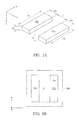
- FIG. 1A is schematic 3-D diagram of a metallic structure according to a first embodiment of the present invention
- FIG. 1B is a schematic top view of the metallic structure according to a first example and a second example of applying the first embodiment
- FIG. 1C is a schematic top view of the metallic structure according to a third example of applying the first embodiment
- FIG. 1D is a schematic top view of the metallic structure according to a fourth example of applying the first embodiment
- FIG. 1E is a schematic top view of the metallic structure according to a fifth example of applying the first embodiment
- FIG. 2A shows distribution curves of x-axis transmittance versus wavelength obtained by simulating the first to fifth examples of applying the first embodiment
- FIG. 2B shows distribution curves of z-axis transmittance versus wavelength obtained by simulating the first to fifth examples of applying the first embodiment
- FIG. 3A is schematic top view of a metallic structure according to a first example of applying a second embodiment of the present invention
- FIG. 3B is a schematic top view of the metallic structure according to a second example of applying the second embodiment
- FIG. 3C is a schematic top view of the metallic structure according to a third example of applying the second embodiment.
- FIG. 3D is a schematic top view of the metallic structure according to a fourth example of applying the second embodiment.
- FIG. 4A shows distribution curves of x-axis transmittance versus wavelength obtained by simulating the first to fourth examples of applying the second embodiment
- FIG. 4B shows distribution curves of z-axis transmittance versus wavelength obtained by simulating the first to fourth examples of applying the second embodiment
- FIG. 5A is schematic top view of a metallic structure according to a first example of applying a third embodiment of the present invention.
- FIG. 5B is a schematic top view of the metallic structure according to a second example of applying the third embodiment.
- FIG. 5C is a schematic top view of the metallic structure according to a third example of applying the third embodiment.
- FIG. 5D is a schematic top view of the metallic structure according to a fourth example of applying the third embodiment.
- FIG. 5E is a schematic top view of the metallic structure according to a fifth example of applying the third embodiment.
- FIG. 5F is a schematic top view of the metallic structure according to a sixth example of applying the third embodiment.
- FIG. 5G is a schematic top view of the metallic structure according to a seventh example of applying the third embodiment.
- FIG. 6A shows distribution curves of x-axis transmittance versus wavelength obtained by simulating the first to seventh examples of applying the third embodiment
- FIG. 6B shows distribution curves of z-axis transmittance versus wavelength obtained by simulating the first to seventh examples of applying the third embodiment
- FIG. 7A is schematic top view of a metallic structure according to an example of applying a fourth embodiment of the present invention.
- FIG. 7B shows distribution curves of x-axis transmittance versus wavelength obtained by simulating the example of applying the fourth embodiment
- FIG. 7C shows distribution curves of z-axis transmittance versus wavelength obtained by simulating the example of applying the fourth embodiment
- FIG. 8A is schematic top view of a metallic structure according to an example of applying a fifth embodiment of the present invention.
- FIG. 8B shows distribution curves of x-axis transmittance versus wavelength obtained by simulating the example of applying the fifth embodiment.
- FIG. 8C shows distribution curves of z-axis transmittance versus wavelength obtained by simulating the example of applying the fifth embodiment.
- Electrons on the surface of metallic materials can strongly interact with electromagnetic fields, depending on its polarization.
- the collective electron motions have plasmonic eigenmodes of which the frequency is proportional to the square root of the electron density that is higher for regular metals and lower for doped semiconductors.
- a typical plasmonic frequency is in the range from ultraviolet to infrared.
- the present invention utilizes the aforementioned interaction to achieve good filtering and polarization as well as high transmission efficiency.
- Electromagnetic force is a long range force, so that the aforementioned interaction does not require a physical contact.
- the multiple metallic blocks or sheets disposed inside or over the light transmissible medium may or may not contact each other, the electrons on one metallic block or sheet can interact with the electromagnetic wave fields which at the same time also interact with the electrons on another block or sheet nearby. These coupled interactions can occur even when there is no physical contact between two blocks/sheets, allowing the surface plasmons to propagate (or the electrons and the electron oscillations to flow) from one block/sheet to another block/sheet.
- the electric field of the electromagnetic wave has a component (vertically polarized wave) perpendicular to the boundary of the block/sheet, and a component (parallel polarized wave) parallel to the boundary of the block/sheet. These coupled interactions through the electric field can be further enhanced by the polarization effect induced at the boundary surface of the blocks/sheets.
- the metallic block of the present invention is referred to a square block, a rectangular block or a block in another shape formed from a metallic material.
- the metallic material is referred to a metal material or a material with partial metallic characters, wherein the metal material can be such as copper, aluminum, alloy, etc., and the material with partial metallic characters can be such as a semiconductor material or a mixture containing the semiconductor material.
- the light transmissible medium of the present invention can be any light transmissible material, such as air, glass, dielectric, etc.
- the electron oscillations When the medium (such as the boundary or width of the metallic block) is changed, the electron oscillations will be reflected or partially reflected. The electron oscillations will vigorously interact with the parallel and perpendicular polarized waves, and respectively affect the transmission and reflection of the parallel and perpendicular polarized waves.
- the geometrical changes of the metallic blocks (such as the changes of respective lengths, widths and thickness thereof) can all affect the electron oscillations and the interactions with the parallel and perpendicular polarized waves of light, and thus affect the transmission, filtering and polarization of light, wherein the interactions can be understood by a finite-difference time-domain (FDTD) simulation.
- FDTD finite-difference time-domain
- a metallic structure of the preset invention is applicable to an opto-electronic apparatus such as a filter, a polarizer, a wave splitter, a sensor or a display, etc.
- the metallic structure of the present invention is used for filtering (splitter) or polarizing an electromagnetic wave, wherein the electromagnetic wave includes a preferable range wavelength which is substantially between 0.1 ⁇ m and 12 ⁇ m, and more preferably, substantially between 0.1 ⁇ m and 2 ⁇ m (as shown in the following simulation results).
- the wavelength range of the electromagnetic wave which can be processed by the metallic structure of the present invention is not limited thereto, and may be the wavelength within any range.
- metallic blocks forming the metallic structures used in examples corresponding to respective embodiments are formed from Al—Cu alloy, and a light transmissible medium used in each example is air, and the metallic blocks can be fixed on an opto-electronic apparatus by means of an appropriate mechanism.
- same reference numbers shown in the figures represent same or similar elements.
- FIG. 1A is schematic 3-D diagram of a metallic structure according to a first embodiment of the present invention
- FIG. 1B is a schematic top view of the metallic structure according to a first example and a second example of applying the first embodiment.
- the first embodiment is a basic metallic structure of the present invention, and for convenience of explanation, a light transmissible medium 100 is omitted in FIG. 1A .
- the basic metallic structure of the present invention is formed from two substantially parallel metallic blocks, including a first metallic block 110 and a second metallic block 120 , used for filtering or polarizing an electromagnetic wave. As shown in FIG.
- the first metallic block 110 and the second metallic block 120 are disposed inside or over a surface of the light transmissible medium 100 , wherein the size of the light transmissible medium 100 is merely used as an example for explanation, and do not intend to limit embodiments of the present invention. In fact, the size of the light transmissible medium 100 may be adjusted in accordance with actual needs. Furthermore, if light transmissible medium 100 fails to provide support to the metallic structure, an appropriate support mechanism is required to be designed additionally, which is well known to those who are skilled in the art and not described herein.
- the first metallic block 110 and the second metallic block 120 are spaced from each other at a predetermined distance d, wherein the electromagnetic wave is incident on surfaces of the first metallic block 110 and the second metallic block 120 and between the first metallic block 110 and the second metallic block 120 .
- the electromagnetic wave After passing through the metallic structure, the electromagnetic wave has a distribution curve of transmittance versus wavelength, wherein the distribution curve has at least one transmittance peak value corresponding to at least one wavelength in a one-to-one manner.
- the predetermined distance d and an averaged width w 1 of the first metallic block 110 satisfies the following relationships: d ⁇ (1) 0.01 ⁇ w 1 ⁇ d (2)
- ⁇ represents one of the at least one wavelength
- the predetermined distance d and the averaged width w 1 of the first metallic block 110 also satisfy the following relationship: d+w 1 ⁇ (3)
- An averaged length 11 of the first metallic block 110 satisfies the following relationship: l 1 ⁇ 2 ⁇ (4)
- ⁇ is corresponding to one (a first transmittance peak value) of the at least one transmittance peak value, and the first transmittance peak value is greater than 10%, and a spectrum half width corresponding to between the wavelength of the first transmittance peak value and the wavelength whose transmittance is 70% of the first transmittance peak value is smaller than 2 ⁇ /3.
- ⁇ is a wavelength desired to be obtained by performing a filtering operation using the metallic structure of the present invention, such as red light wavelength, green light wavelength or blue light wavelength, etc.
- a transmittance is a ratio of the intensities of the electromagnetic wave before or after entering an area Ac between the second metallic block 120 and the first metallic block 110 plus an area Ab of the first metallic block 110 . Since the predetermined distance d is smaller than ⁇ , electrons or plasmons on the second metallic block 120 and the first metallic block 110 are coupled with the electric field of the electromagnetic wave, such that the metallic structure of the present invention has excellent filtering and polarizing effects.
- the transmittance can be divided into a component (referred as a x-axis transmittance, as shown in FIG.
- the filtering and polarizing effects of the metallic structure of this embodiment can be known, wherein the x-axis transmittance component and the z-axis transmittance component may exhibit the polarizing effect of the metallic structure, and the transmittance at a peak value, a valley value or zero may exhibit the filtering effect.
- the transmittance is at a peak value, it means that the electromagnetic wave with a wavelength corresponding to the transmittance can pass through the metallic structure.
- the transmittance is at a valley value or zero, it means that the electromagnetic wave with a wavelength corresponding to the transmittance is filtered out by the metallic structure.
- FIG. 2A shows distribution curves of x-axis transmittance versus wavelength obtained by simulating the first to fifth examples of applying the first embodiment
- FIG. 2B shows distribution curves of z-axis transmittance versus wavelength obtained by simulating first to fifth examples of applying the first embodiment.
- the length 11 of the first metallic block 110 is 0.32 ⁇ m; the width w 1 thereof is 0.16 ⁇ m; and the thickness t 1 thereof is 0.08 ⁇ m.
- the length 12 of the second metallic block 120 is 0.32 ⁇ m; the width w 2 thereof is 0.16 ⁇ m; and the thickness t 2 thereof is 0.08 ⁇ m.
- the predetermined distance d between the first metallic block 110 and the second metallic block 120 is 0.32 ⁇ m.
- the curve corresponding to the first example has a plurality of transmittance peak values.
- the wavelength ⁇ corresponding thereto is 1.4 ⁇ m, and thus the length 11 , the width w 1 of the first metallic block 110 , and the predetermined distance d satisfy the aforementioned equations (1)-(4).
- the curve corresponding to the first example has many transmittance peak values.
- the wavelength ⁇ corresponding thereto is 1.45 ⁇ m, and thus the length 11 and the width w 1 of the first metallic block 110 , and hence the predetermined distance d satisfy the aforementioned equations (1)-(4).
- the wavelength ⁇ corresponding thereto is 0.8 ⁇ m, which is about equal to twice of the length 11 (0.32 ⁇ m), in which the phenomenon is relevant to the surface plasmons discussed above.
- the metallic structure of this example has good filtering and polarizing effects.
- the second example is different from the first example in that the thickness t 1 of the first metallic block 110 and the thickness t 2 of the second metallic block 120 both are 0.16 ⁇ m.
- the thickness of the metallic block is generally smaller than the desired wavelength ⁇ , but the present invention is not limited thereto.
- FIG. 1C is a schematic top view of the metallic structure according to the third example of applying the first embodiment.
- the length 11 of the first metallic block 110 is 0.32 ⁇ m; the width w 1 thereof is 0.16 ⁇ m; and the thickness t 1 thereof is 0.08 ⁇ m.
- the length 12 of the second metallic block 120 is 4.0 ⁇ m; the width w 2 thereof is 1.84 ⁇ m; and the thickness t 2 thereof is 0.08 ⁇ m.
- the predetermined distance d between the first metallic block 110 and the second metallic block 120 is 0.32 ⁇ m.
- FIG. 1D is a schematic top view of the metallic structure according to the fourth example of applying the first embodiment.
- the length 11 of the first metallic block 110 is 0.32 ⁇ m; the width w 1 thereof is 0.16 ⁇ m; and the thickness t 1 thereof is 0.08 ⁇ m.
- the length 12 of the second metallic block 120 is 0.32 ⁇ m; the width w 2 thereof is 1.84 ⁇ m; and the thickness t 2 thereof is 0.08 ⁇ m.
- the predetermined distance d between the first metallic block 110 and the second metallic block 120 is 0.32 ⁇ m.
- FIG. 1E is a schematic top view of the metallic structure according to the fifth example of applying the first embodiment, wherein the first metallic block 110 is disposed between the second metallic block 120 and a third metallic block 130 .
- the length 11 of the first metallic block 110 is 0.32 ⁇ m; the width w 1 thereof is 0.16 ⁇ m; and the thickness t 1 thereof is 0.08 ⁇ m.
- the length 12 of the second metallic block 120 is 0.32 ⁇ m; the width w 2 thereof is 0.16 ⁇ m; and the thickness t 2 thereof is 0.08 ⁇ m.
- the length 13 of the third metallic block 130 is 0.32 ⁇ m; the width w 3 thereof is 0.16 ⁇ m; and the thickness t 3 thereof is 0.08 ⁇ m.
- the predetermined distance d between the first metallic block 110 and the second metallic block 120 is 0.32 ⁇ m.
- the predetermined distance d between the first metallic block 110 and the third metallic block 130 is 0.32 ⁇ m.
- the length 11 and the width w 1 of the first metallic block 110 , and the predetermined distance d of this example satisfy the aforementioned equations (1)-(4); the length 13 and the width w 3 of the third metallic block 130 , and the predetermined distance d also satisfy the aforementioned equations (1)-(4); and the metallic structure of this example has good filtering and polarizing effects.
- FIG. 3A is schematic top view of a metallic structure according to a first example of applying a second embodiment of the present invention.
- the second embodiment is different from the first embodiment in that the metallic structure further includes a third metallic block 130 .
- the third metallic block 130 is disposed inside or over the light transmissible medium 100 and is adjacent to one side of the first metallic block 110 and the second metallic block 120 .
- An extension of the third metallic block 130 is substantially perpendicular to extensions of the first metallic block 110 and the second metallic block 120 , and the third metallic block 130 may or may not simultaneously contact the first metallic block 110 and the second metallic block 120 .
- FIG. 4A shows distribution curves of x-axis transmittance versus wavelength obtained by simulating first to fourth examples of applying the second embodiment
- FIG. 4B shows distribution curves of z-axis transmittance versus wavelength obtained by simulating the first to fourth examples of applying the second embodiment.
- the third metallic block 130 does not contact the first metallic block 110 and the second metallic block 120 .
- the length 11 of the first metallic block 110 is 0.3 ⁇ m; the width w 1 thereof is 0.16 ⁇ m; and the thickness t 1 thereof is 0.08 ⁇ m.
- the length 12 of the second metallic block 120 is 0.3 ⁇ m; the width w 2 thereof is 0.16 ⁇ m; and the thickness t 2 thereof is 0.08 ⁇ m.
- the length 13 of the third metallic block 130 is 0.3 ⁇ m; the width w 3 thereof is 0.16 ⁇ m; and the thickness t 3 thereof is 0.08 ⁇ m.
- the predetermined distance d between the first metallic block 110 and the second metallic block 120 is 0.32 ⁇ m.
- FIG. 3B is a schematic top view of the metallic structure according to the second example of applying the second embodiment, wherein the third metallic block 130 contacts the first metallic block 110 but does not contact the second metallic block 120 .
- the length 11 of the first metallic block 110 is 0.31 ⁇ m; the width w 1 thereof is 0.16 ⁇ m; and the thickness t 1 thereof is 0.08 ⁇ m.
- the length 12 of the second metallic block 120 is 0.3 ⁇ m; the width w 2 thereof is 0.16 ⁇ m; and the thickness t 2 thereof is 0.08 ⁇ m.
- the length 13 of the third metallic block 130 is 0.47 ⁇ m; the width w 3 thereof is 0.16 ⁇ m; and the thickness t 3 thereof is 0.08 ⁇ m.
- the predetermined distance d between the first metallic block 110 and the second metallic block 120 is 0.32 ⁇ m.
- FIG. 3C is a schematic top view of the metallic structure according to the third example of applying the second embodiment, wherein the third metallic block 130 simultaneously contacts the first metallic block 110 and the second metallic block 120 .
- the length 11 of the first metallic block 110 is 0.31 ⁇ m; the width w 1 thereof is 0.16 ⁇ m; and the thickness t 1 thereof is 0.08 ⁇ m.
- the length 12 of the second metallic block 120 is 0.31 ⁇ m; the width w 2 thereof is 0.16 ⁇ m; and the thickness t 2 thereof is 0.08 ⁇ m.
- the length 13 of the third metallic block 130 is 0.64 ⁇ m; the width w 3 thereof is 0.16 ⁇ m; and the thickness t 3 thereof is 0.08 ⁇ m.
- the predetermined distance d between the first metallic block 110 and the second metallic block 120 is 0.32 ⁇ m.
- FIG. 3D is a schematic top view of the metallic structure according to the fourth example of applying the second embodiment, wherein the third metallic block 130 does not contact the first metallic block 110 but contacts the second metallic block 120 , and the size of the second metallic block 120 and the third metallic block 130 are much greater than that of the first metallic block 110 .
- the length 11 of the first metallic block 110 is 0.3 ⁇ m; the width w 1 thereof is 0.16 ⁇ m; and the thickness t 1 thereof is 0.08 ⁇ m.
- the length 12 of the second metallic block 120 is 2.16 ⁇ m; the width w 2 thereof is 1.84 ⁇ m; and the thickness t 2 thereof is 0.08 ⁇ m.
- the length 13 of the third metallic block 130 is 4.00 ⁇ m; the width w 3 thereof is 1.84 ⁇ m; and the thickness t 3 thereof is 0.08 ⁇ m.
- the predetermined distance d between the first metallic block 110 and the second metallic block 120 is 0.32 ⁇ m.
- FIG. 5A is schematic top view of a metallic structure according to a first example of applying a third embodiment of the present invention.
- the third embodiment is different from the second embodiment in that the metallic structure further includes a fourth metallic block 140 .
- the fourth metallic block 140 is disposed inside or over the light transmissible medium 100 and is adjacent to the other side of the first metallic block 110 and the second metallic block 120 .
- An extension of the fourth metallic block 140 is substantially perpendicular to extensions of the first metallic block 110 and the second metallic block 120 , and the fourth metallic block 140 may or may not simultaneously contact the first metallic block 110 and the second metallic block 120 .
- FIG. 6A shows distribution curves of x-axis transmittance versus wavelength obtained by simulating first to seventh examples of applying the third embodiment
- FIG. 6B shows distribution curves of z-axis transmittance versus wavelength obtained by simulating the first to seventh examples of applying the third embodiment.
- the third metallic block 130 and the fourth metallic block 140 do not contact the first metallic block 110 and the second metallic block 120 , wherein the length 11 of the first metallic block 110 is 0.3 ⁇ m; the width w 1 thereof is 0.16 ⁇ m; and the thickness t 1 thereof is 0.08 ⁇ m.
- the length 12 of the second metallic block 120 is 0.3 ⁇ m; the width w 2 thereof is 0.16 ⁇ m; and the thickness t 2 thereof is 0.08 ⁇ m.
- the length 13 of the third metallic block 130 is 0.3 ⁇ m; the width w 3 thereof is 0.16 ⁇ m; and the thickness t 3 thereof is 0.08 ⁇ m.
- the length 14 of the fourth metallic block 140 is 0.3 ⁇ m; the width w 4 thereof is 0.16 ⁇ m; and the thickness t 4 thereof is 0.08 ⁇ m.
- the predetermined distance d between the first metallic block 110 and the second metallic block 120 is 0.32 ⁇ m.
- the length 11 , the width w 1 of the first metallic block 110 , and the predetermined distance d of this example satisfy the aforementioned equations (1)-(4), and the metallic structure of this example has good filtering and polarizing effects. It is worthy of being noted that, since the metallic structure of this embodiment is symmetrical to the x axis and the z axis, the distribution curve of x-axis transmittance versus wavelength is identical to that of z-axis transmittance versus wavelength.
- FIG. 5B is a schematic top view of the metallic structure according to the second example of applying the third embodiment, wherein the third metallic block 130 contacts the first metallic block 110 but does not contact the second metallic block 120 , and the fourth metallic block 140 does not contact the first metallic block 110 and the second metallic block 120 .
- the length 11 of the first metallic block 110 is 0.31 ⁇ m; the width w 1 thereof is 0.16 ⁇ m; and the thickness t 1 thereof is 0.08 ⁇ m.
- the length 12 of the second metallic block 120 is 0.3 ⁇ m; the width w 2 thereof is 0.16 ⁇ m; and the thickness t 2 thereof is 0.08 ⁇ m.
- the length 13 of the third metallic block 130 is 0.47 ⁇ m; the width w 3 thereof is 0.16 ⁇ m; and the thickness t 3 thereof is 0.08 ⁇ m.
- the length 14 of the fourth metallic block 140 is 0.3 ⁇ m; the width w 4 thereof is 0.16 ⁇ m; and the thickness t 4 thereof is 0.08 ⁇ m.
- the predetermined distance d between the first metallic block 110 and the second metallic block 120 is 0.32 ⁇ m.
- FIG. 5C is a schematic top view of the metallic structure according to the third example of applying the third embodiment, wherein the third metallic block 130 contacts the first metallic block 110 but does not contact the second metallic block 120 , and the fourth metallic block 140 contacts the first metallic block 110 but does not contact the second metallic block 120 .
- the length 11 of the first metallic block 110 is 0.32 ⁇ m; the width w 1 thereof is 0.16 ⁇ m; and the thickness t 1 thereof is 0.08 ⁇ m.
- the length 12 of the second metallic block 120 is 0.3 ⁇ m; the width w 2 thereof is 0.16 ⁇ m; and the thickness t 2 thereof is 0.08 ⁇ m.
- the length 13 of the third metallic block 130 is 0.47 ⁇ m; the width w 3 thereof is 0.16 ⁇ m; and the thickness t 3 thereof is 0.08 ⁇ m.
- the length 14 of the third metallic block 130 is 0.47 ⁇ m; the width w 4 thereof is 0.16 ⁇ m; and the thickness t 4 thereof is 0.08 ⁇ m.
- the predetermined distance d between the first metallic block 110 and the second metallic block 120 is 0.32 ⁇ m.
- FIG. 5D is a schematic top view of the metallic structure according to the fourth example of applying the third embodiment, wherein the third metallic block 130 contacts the first metallic block 110 but does not contact the second metallic block 120 , and the fourth metallic block 140 does not contact the first metallic block 110 but contacts the second metallic block 120 .
- the length 11 of the first metallic block 110 is 0.31 ⁇ m; the width w 1 thereof is 0.16 ⁇ m; and the thickness t 1 thereof is 0.08 ⁇ m.
- the length 12 of the second metallic block 120 is 0.31 ⁇ m; the width w 2 thereof is 0.16 ⁇ m; and the thickness t 2 thereof is 0.08 ⁇ m.
- the length 13 of the third metallic block 130 is 0.47 ⁇ m; the width w 3 thereof is 0.16 ⁇ m; and the thickness t 3 thereof is 0.08 ⁇ m.
- the length 14 of the third metallic block 130 is 0.47 ⁇ m; the width w 4 thereof is 0.16 ⁇ m; and the thickness t 4 thereof is 0.08 ⁇ m.
- the predetermined distance d between the first metallic block 110 and the second metallic block 120 is 0.32 ⁇ m.
- the length 11 , the width w 1 of the first metallic block 110 , and the predetermined distance d of this example satisfy the aforementioned equations (1)-(4), and the metallic structure of this example has good filtering and polarizing effects. It is worthy of being noted that, since the metallic structure of this embodiment is symmetrical to its center point, the distribution curve of x-axis transmittance versus wavelength is identical to that of z-axis transmittance versus wavelength.
- FIG. 5E is a schematic top view of the metallic structure according to the fifth example of applying the third embodiment, wherein the third metallic block 130 contacts the first metallic block 110 and the second metallic block 120 , and the fourth metallic block 140 contacts the first metallic block 110 but does not contact the second metallic block 120 .
- the length 11 of the first metallic block 110 is 0.32 ⁇ m; the width w 1 thereof is 0.16 ⁇ m; and the thickness t 1 thereof is 0.08 ⁇ m.
- the length 12 of the second metallic block 120 is 0.31 ⁇ m; the width w 2 thereof is 0.16 ⁇ m; and the thickness t 2 thereof is 0.08 ⁇ m.
- the length 13 of the third metallic block 130 is 0.64 ⁇ m; the width w 3 thereof is 0.16 ⁇ m; and the thickness t 3 thereof is 0.08 ⁇ m.
- the length 14 of the third metallic block 130 is 0.47 ⁇ m; the width w 4 thereof is 0.16 ⁇ m; and the thickness t 4 thereof is 0.08 ⁇ m.
- the predetermined distance d between the first metallic block 110 and the second metallic block 120 is 0.32 ⁇ m.
- the length 11 , the width w 1 of the first metallic block 110 , and the predetermined distance d of this example satisfy the aforementioned equations (1)-(4), and the metallic structure of this example has good filtering and polarizing effects. It is worthy of being noted that, since the metallic structure of this embodiment is symmetrical to its center point, the distribution curve of x-axis transmittance versus wavelength is identical to that of z-axis transmittance versus wavelength.
- FIG. 5F is a schematic top view of the metallic structure according to the sixth example of applying the third embodiment, wherein the third metallic block 130 and the fourth metallic block 140 simultaneously contact the first metallic block 110 and the second metallic block 120 .
- the length 11 of the first metallic block 110 is 0.32 ⁇ m; the width w 1 thereof is 0.16 ⁇ m; and the thickness t 1 thereof is 0.08 ⁇ m.
- the length 12 of the second metallic block 120 is 0.32 ⁇ m; the width w 2 thereof is 0.16 ⁇ m; and the thickness t 2 thereof is 0.08 ⁇ m.
- the length 13 of the third metallic block 130 is 0.64 ⁇ m; the width w 3 thereof is 0.16 ⁇ m; and the thickness t 3 thereof is 0.08 ⁇ m.
- the length 14 of the third metallic block 130 is 0.64 ⁇ m; the width w 4 thereof is 0.16 ⁇ m; and the thickness t 4 thereof is 0.08 ⁇ m.
- the predetermined distance d between the first metallic block 110 and the second metallic block 120 is 0.32 ⁇ m.
- the length 11 , the width w 1 of the first metallic block 110 , and the predetermined distance d of this example satisfy the aforementioned equations (1)-(4), and the metallic structure of this example has good filtering and polarizing effects. It is worthy of being noted that, since the metallic structure of this embodiment is symmetrical to its center point, the distribution curve of x-axis transmittance versus wavelength is identical to that of z-axis transmittance versus wavelength.
- FIG. 5G is a schematic top view of the metallic structure according to the seventh example of applying the third embodiment, wherein the third metallic block 130 and the fourth metallic block 140 do not contact the first metallic block 110 but contact the second metallic block 120 , and the size of the second metallic block 120 , the third metallic block 130 , and the forth metallic block are much greater than that of the first metallic block 110 .
- the length 11 of the first metallic block 110 is 0.6 ⁇ m; the width w 1 thereof is 0.16 ⁇ m; and the thickness t 1 thereof is 0.08 ⁇ m.
- the length 12 of the second metallic block 120 is 0.64 ⁇ m; the width w 2 thereof is 1.84 ⁇ m; and the thickness t 2 thereof is 0.08 ⁇ m.
- the length 13 of the third metallic block 130 is 4.00 ⁇ m; the width w 3 thereof is 1.68 ⁇ m; and the thickness t 3 thereof is 0.08 ⁇ m.
- the length 14 of the third metallic block 130 is 4.00 ⁇ m; the width w 4 thereof is 1.68 ⁇ m; and the thickness t 4 thereof is 0.08 ⁇ m.
- the predetermined distance d between the first metallic block 110 and the second metallic block 120 is 0.32 ⁇ m.
- Each of the aforementioned metallic structures of the respective embodiments can be repetitively formed as a metallic array including a plurality of array units.
- Each array unit includes the aforementioned first metallic block, the aforementioned second metallic block, and/or the aforementioned third metallic block and/or the aforementioned first metallic block.
- These metallic blocks also can be arranged in the respective patterns shown in the aforementioned embodiments (examples).
- the metallic structure shown in the first example of the third embodiment is used again for explaining the metallic array.
- FIG. 7A is schematic top view of a metallic structure according to an example of applying a fourth embodiment of the present invention, wherein the metallic array includes a plurality of metallic units 200 , and each metallic unit 200 includes the first, second, third, and fourth metallic blocks shown in the first example of applying the third embodiment.
- FIG. 7B shows distribution curves of x-axis transmittance versus wavelength obtained by simulating the example of applying the fourth embodiment
- FIG. 7C shows distribution curves of z-axis transmittance versus wavelength obtained by simulating the example of applying the fourth embodiment.
- Each of the aforementioned metallic structures of the respective embodiments can be disposed in a metallic frame formed from a metallic material.
- a metallic structure of this embodiment includes the aforementioned first metallic block, the aforementioned second metallic block, and/or the aforementioned third metallic block and/or the aforementioned forth metallic block. These metallic blocks also can be arranged in the respective patterns shown in the aforementioned embodiments (examples).
- disposing the metallic structure shown in the first example of the first embodiment in a metallic frame is used as an example for explanation.
- FIG. 8A is schematic top view of a metallic structure according to an example of applying a fifth embodiment of the present invention, wherein the first metallic block 110 and the second metallic block 120 shown in the first example of applying the first embodiment is disposed in a metallic frame 210 .
- FIG. 8B shows distribution curves of x-axis transmittance versus wavelength obtained by simulating the example of applying the fifth embodiment
- FIG. 8C shows distribution curves of z-axis transmittance versus wavelength obtained by simulating the example of applying the fifth embodiment.
Abstract
Description
d+w<λ.
d<λ (1)
0.01λ<w1<d (2)
d+w1<λ (3)
l1<2λ (4)
Claims (24)
d<λ;0.01λ<w<d,
l<2λ,
d+w<λ.
d<λ;0.01λ<w<d,
l<2λ,
d+w<λ.
Applications Claiming Priority (3)
| Application Number | Priority Date | Filing Date | Title |
|---|---|---|---|
| TW100142940A TWI454755B (en) | 2011-11-23 | 2011-11-23 | Metallic structure and opto-electronic apparatus |
| TW100142940A | 2011-11-23 | ||
| TW100142940 | 2011-11-23 |
Publications (2)
| Publication Number | Publication Date |
|---|---|
| US20130128356A1 US20130128356A1 (en) | 2013-05-23 |
| US9170358B2 true US9170358B2 (en) | 2015-10-27 |
Family
ID=47709757
Family Applications (1)
| Application Number | Title | Priority Date | Filing Date |
|---|---|---|---|
| US13/657,931 Active 2033-07-13 US9170358B2 (en) | 2011-11-23 | 2012-10-23 | Metallic structure and opto-electronic apparatus |
Country Status (6)
| Country | Link |
|---|---|
| US (1) | US9170358B2 (en) |
| EP (1) | EP2597498A1 (en) |
| JP (1) | JP5805054B2 (en) |
| KR (1) | KR101463605B1 (en) |
| CN (1) | CN103138033B (en) |
| TW (1) | TWI454755B (en) |
Cited By (1)
| Publication number | Priority date | Publication date | Assignee | Title |
|---|---|---|---|---|
| US11397331B2 (en) | 2018-10-22 | 2022-07-26 | California Institute Of Technology | Color and multi-spectral image sensor based on 3D engineered material |
Families Citing this family (3)
| Publication number | Priority date | Publication date | Assignee | Title |
|---|---|---|---|---|
| JP2017527857A (en) * | 2014-09-15 | 2017-09-21 | カリフォルニア インスティチュート オブ テクノロジー | Simultaneous polarization and wavefront control using planar devices |
| CN107783309B (en) * | 2017-11-23 | 2019-10-11 | 武汉大学 | Metal nano brick array structure and its application as polarizing beam splitter |
| US10670739B2 (en) | 2018-07-17 | 2020-06-02 | Polimaster Holdings Corporation | Gamma radiation and neutron radiation detector |
Citations (13)
| Publication number | Priority date | Publication date | Assignee | Title |
|---|---|---|---|---|
| US20040096136A1 (en) * | 2002-11-18 | 2004-05-20 | Harmeet Singh | Integrated polarization rotator |
| JP2007272016A (en) | 2006-03-31 | 2007-10-18 | Optoelectronic Industry & Technology Development Association | Polarizing plate |
| US20080217558A1 (en) | 2005-09-22 | 2008-09-11 | Koninklijke Philips Electronics, N.V. | Luminescence Sensor Comprising at Least Two Wire Grids |
| US7511884B2 (en) * | 2003-02-27 | 2009-03-31 | Asml Netherlands B.V. | Stationary and dynamic radial transverse electric polarizer for high numerical aperture systems |
| JP2009223074A (en) | 2008-03-18 | 2009-10-01 | Ricoh Co Ltd | Polarization converting element |
| US7619816B2 (en) * | 2004-12-15 | 2009-11-17 | Api Nanofabrication And Research Corp. | Structures for polarization and beam control |
| US7683982B2 (en) * | 2007-02-16 | 2010-03-23 | Samsung Electronics Co., Ltd. | Active reflective polarizer, liquid crystal display employing the same and method for the same |
| US7755718B2 (en) * | 2007-08-10 | 2010-07-13 | Seiko Epson Corporation | Optical element, liquid crystal device, and display |
| US7755717B2 (en) * | 2007-03-07 | 2010-07-13 | Seiko Epson Corporation | Polarizing element, polarizing element manufacturing method, liquid crystal device, and projection display |
| JP2010186164A (en) | 2009-01-13 | 2010-08-26 | Canon Inc | Optical element |
| US20110043813A1 (en) * | 2009-08-21 | 2011-02-24 | Canon Kabushiki Kaisha | Optical apparatus, optical detector, optical modulator, imaging apparatus, and camera |
| US20110080640A1 (en) | 2008-04-03 | 2011-04-07 | Asahi Glass Company, Limited | Wire-grid polarizer and process for producing the same |
| JP2011164206A (en) | 2010-02-05 | 2011-08-25 | National Institute For Materials Science | Polarization control element |
-
2011
- 2011-11-23 TW TW100142940A patent/TWI454755B/en active
-
2012
- 2012-10-23 US US13/657,931 patent/US9170358B2/en active Active
- 2012-11-16 EP EP12192929.3A patent/EP2597498A1/en active Pending
- 2012-11-19 JP JP2012253346A patent/JP5805054B2/en active Active
- 2012-11-19 KR KR1020120131163A patent/KR101463605B1/en active IP Right Grant
- 2012-11-23 CN CN201210485647.9A patent/CN103138033B/en active Active
Patent Citations (14)
| Publication number | Priority date | Publication date | Assignee | Title |
|---|---|---|---|---|
| US20040096136A1 (en) * | 2002-11-18 | 2004-05-20 | Harmeet Singh | Integrated polarization rotator |
| US7511884B2 (en) * | 2003-02-27 | 2009-03-31 | Asml Netherlands B.V. | Stationary and dynamic radial transverse electric polarizer for high numerical aperture systems |
| US7619816B2 (en) * | 2004-12-15 | 2009-11-17 | Api Nanofabrication And Research Corp. | Structures for polarization and beam control |
| US20080217558A1 (en) | 2005-09-22 | 2008-09-11 | Koninklijke Philips Electronics, N.V. | Luminescence Sensor Comprising at Least Two Wire Grids |
| JP2007272016A (en) | 2006-03-31 | 2007-10-18 | Optoelectronic Industry & Technology Development Association | Polarizing plate |
| US7683982B2 (en) * | 2007-02-16 | 2010-03-23 | Samsung Electronics Co., Ltd. | Active reflective polarizer, liquid crystal display employing the same and method for the same |
| US7755717B2 (en) * | 2007-03-07 | 2010-07-13 | Seiko Epson Corporation | Polarizing element, polarizing element manufacturing method, liquid crystal device, and projection display |
| US7755718B2 (en) * | 2007-08-10 | 2010-07-13 | Seiko Epson Corporation | Optical element, liquid crystal device, and display |
| JP2009223074A (en) | 2008-03-18 | 2009-10-01 | Ricoh Co Ltd | Polarization converting element |
| US20110080640A1 (en) | 2008-04-03 | 2011-04-07 | Asahi Glass Company, Limited | Wire-grid polarizer and process for producing the same |
| JP2010186164A (en) | 2009-01-13 | 2010-08-26 | Canon Inc | Optical element |
| US20110273771A1 (en) | 2009-01-13 | 2011-11-10 | Canon Kabushiki Kaisha | Optical element |
| US20110043813A1 (en) * | 2009-08-21 | 2011-02-24 | Canon Kabushiki Kaisha | Optical apparatus, optical detector, optical modulator, imaging apparatus, and camera |
| JP2011164206A (en) | 2010-02-05 | 2011-08-25 | National Institute For Materials Science | Polarization control element |
Non-Patent Citations (4)
| Title |
|---|
| English translation of abstract of JP 2007-272016 (published Oct. 18, 2007). |
| English translation of abstract of JP 2009-223074 (published Oct. 1, 2009). |
| English translation of abstract of JP 2010-186164 (published Aug. 26, 2010). |
| English translation of abstract of JP 2011-164206 (published Aug. 25, 2011). |
Cited By (1)
| Publication number | Priority date | Publication date | Assignee | Title |
|---|---|---|---|---|
| US11397331B2 (en) | 2018-10-22 | 2022-07-26 | California Institute Of Technology | Color and multi-spectral image sensor based on 3D engineered material |
Also Published As
| Publication number | Publication date |
|---|---|
| TWI454755B (en) | 2014-10-01 |
| JP2013109349A (en) | 2013-06-06 |
| KR101463605B1 (en) | 2014-11-20 |
| CN103138033B (en) | 2016-04-20 |
| US20130128356A1 (en) | 2013-05-23 |
| EP2597498A1 (en) | 2013-05-29 |
| KR20130057398A (en) | 2013-05-31 |
| CN103138033A (en) | 2013-06-05 |
| JP5805054B2 (en) | 2015-11-04 |
| TW201321801A (en) | 2013-06-01 |
Similar Documents
| Publication | Publication Date | Title |
|---|---|---|
| Zhang et al. | Large group delay in a microwave metamaterial analog of electromagnetically induced transparency | |
| Subramania et al. | Nonresonant broadband funneling of light via ultrasubwavelength channels | |
| US9170358B2 (en) | Metallic structure and opto-electronic apparatus | |
| CN106887665B (en) | All-dielectric metamaterial EIT (electromagnetic interference tomography) resonance device | |
| Thirupathaiah et al. | Concurrent dual band filters using plasmonic slot waveguide | |
| Lee et al. | Polarization-independent electromagnetically induced transparency-like transmission in coupled guided-mode resonance structures | |
| He et al. | Reconfigurable terahertz grating with enhanced transmission of TE polarized light | |
| Han et al. | Plasmonic ultra-broadband polarizers based on Ag nano wire-slit arrays | |
| KR20130140327A (en) | Terahertz waves polarizer using extraordinary optical transmission and fabrication method of the same | |
| Chen et al. | Symmetry breaking induced mode splitting based on a plasmonic waveguide system | |
| Tserkezis et al. | Tailoring plasmons with metallic nanorod arrays | |
| Gao et al. | Extraordinary optical transmission for TE wave through metallic sub-wavelength grating with slits filled with dielectric | |
| Park et al. | Tuning optical absorption in an ultrathin lossy film by use of a metallic metamaterial mirror | |
| US9229134B2 (en) | Opto-electronic apparatus with metallic structure | |
| Beruete et al. | High numerical aperture and low-loss negative refraction based on the fishnet rich anisotropy | |
| Abdulnabi et al. | Theoretical investigation of a nano scale all-optical 1× 2 demultiplexer | |
| Zhuldybina et al. | Mass-production of terahertz devices | |
| Navarro-Cia et al. | Numerical and experimental parametric analysis of anomalous enhanced transmission through subwavelength apertures | |
| Yu et al. | Transmissive color filtering using plasmonic multilayer structure | |
| Su et al. | Two-beam emitting via a single subwavelength metal slit surrounded by mixed-period dielectric grooves | |
| Singh et al. | Resonant field enhancement of terahertz waves in subwavelength plasmonic structures | |
| Paulsen | Design techniques for terahertz plasmonic filters | |
| Arkhipova et al. | Observation of linear and nonlinear light localization at the edges of moir\'e lattices | |
| Subramania et al. | Epsilon near zero material for electromagnetic energy transport through sub-wavelength channels. | |
| Huang et al. | Theory of light transmission properties through fanshaped metallic grating |
Legal Events
| Date | Code | Title | Description |
|---|---|---|---|
| AS | Assignment |
Owner name: NATIONAL CHENG KUNG UNIVERSITY, TAIWAN Free format text: ASSIGNMENT OF ASSIGNORS INTEREST;ASSIGNOR:CHEN, KUAN-REN;REEL/FRAME:029171/0534 Effective date: 20121001 |
|
| STCF | Information on status: patent grant |
Free format text: PATENTED CASE |
|
| MAFP | Maintenance fee payment |
Free format text: PAYMENT OF MAINTENANCE FEE, 4TH YR, SMALL ENTITY (ORIGINAL EVENT CODE: M2551); ENTITY STATUS OF PATENT OWNER: SMALL ENTITY Year of fee payment: 4 |
|
| MAFP | Maintenance fee payment |
Free format text: PAYMENT OF MAINTENANCE FEE, 8TH YR, SMALL ENTITY (ORIGINAL EVENT CODE: M2552); ENTITY STATUS OF PATENT OWNER: SMALL ENTITY Year of fee payment: 8 |