US9166657B2 - Radio frequency shield with proximity change alert for a contactless data carrier - Google Patents
Radio frequency shield with proximity change alert for a contactless data carrier Download PDFInfo
- Publication number
- US9166657B2 US9166657B2 US13/695,472 US201113695472A US9166657B2 US 9166657 B2 US9166657 B2 US 9166657B2 US 201113695472 A US201113695472 A US 201113695472A US 9166657 B2 US9166657 B2 US 9166657B2
- Authority
- US
- United States
- Prior art keywords
- antenna
- switching
- radio frequency
- signal
- module
- Prior art date
- Legal status (The legal status is an assumption and is not a legal conclusion. Google has not performed a legal analysis and makes no representation as to the accuracy of the status listed.)
- Expired - Fee Related, expires
Links
- 230000008859 change Effects 0.000 title description 3
- 238000004891 communication Methods 0.000 claims abstract description 150
- 238000000034 method Methods 0.000 claims abstract description 55
- 238000001514 detection method Methods 0.000 claims description 131
- 230000008878 coupling Effects 0.000 claims description 36
- 238000010168 coupling process Methods 0.000 claims description 36
- 238000005859 coupling reaction Methods 0.000 claims description 36
- 230000001960 triggered effect Effects 0.000 claims description 20
- 238000010586 diagram Methods 0.000 description 26
- 238000010276 construction Methods 0.000 description 16
- 230000008569 process Effects 0.000 description 6
- 238000012545 processing Methods 0.000 description 6
- 238000005516 engineering process Methods 0.000 description 5
- 230000005540 biological transmission Effects 0.000 description 4
- 238000013461 design Methods 0.000 description 4
- 230000006855 networking Effects 0.000 description 4
- 238000003780 insertion Methods 0.000 description 2
- 230000037431 insertion Effects 0.000 description 2
- 238000004519 manufacturing process Methods 0.000 description 2
- 239000000654 additive Substances 0.000 description 1
- 230000000996 additive effect Effects 0.000 description 1
- 238000004458 analytical method Methods 0.000 description 1
- 230000002457 bidirectional effect Effects 0.000 description 1
- 230000001419 dependent effect Effects 0.000 description 1
- 230000000694 effects Effects 0.000 description 1
- 230000006872 improvement Effects 0.000 description 1
- 230000004048 modification Effects 0.000 description 1
- 238000012986 modification Methods 0.000 description 1
- 230000001681 protective effect Effects 0.000 description 1
- 230000004044 response Effects 0.000 description 1
- 230000003068 static effect Effects 0.000 description 1
- 238000006467 substitution reaction Methods 0.000 description 1
Images


Classifications
-
- H—ELECTRICITY
- H04—ELECTRIC COMMUNICATION TECHNIQUE
- H04B—TRANSMISSION
- H04B7/00—Radio transmission systems, i.e. using radiation field
- H04B7/02—Diversity systems; Multi-antenna system, i.e. transmission or reception using multiple antennas
- H04B7/04—Diversity systems; Multi-antenna system, i.e. transmission or reception using multiple antennas using two or more spaced independent antennas
- H04B7/0404—Diversity systems; Multi-antenna system, i.e. transmission or reception using multiple antennas using two or more spaced independent antennas the mobile station comprising multiple antennas, e.g. to provide uplink diversity
-
- G—PHYSICS
- G06—COMPUTING; CALCULATING OR COUNTING
- G06K—GRAPHICAL DATA READING; PRESENTATION OF DATA; RECORD CARRIERS; HANDLING RECORD CARRIERS
- G06K7/00—Methods or arrangements for sensing record carriers, e.g. for reading patterns
- G06K7/0008—General problems related to the reading of electronic memory record carriers, independent of its reading method, e.g. power transfer
-
- G—PHYSICS
- G06—COMPUTING; CALCULATING OR COUNTING
- G06K—GRAPHICAL DATA READING; PRESENTATION OF DATA; RECORD CARRIERS; HANDLING RECORD CARRIERS
- G06K7/00—Methods or arrangements for sensing record carriers, e.g. for reading patterns
- G06K7/10—Methods or arrangements for sensing record carriers, e.g. for reading patterns by electromagnetic radiation, e.g. optical sensing; by corpuscular radiation
- G06K7/10009—Methods or arrangements for sensing record carriers, e.g. for reading patterns by electromagnetic radiation, e.g. optical sensing; by corpuscular radiation sensing by radiation using wavelengths larger than 0.1 mm, e.g. radio-waves or microwaves
- G06K7/10316—Methods or arrangements for sensing record carriers, e.g. for reading patterns by electromagnetic radiation, e.g. optical sensing; by corpuscular radiation sensing by radiation using wavelengths larger than 0.1 mm, e.g. radio-waves or microwaves using at least one antenna particularly designed for interrogating the wireless record carriers
Definitions
- the present invention relates to radio frequency identification (RFID) and, more particularly, to a method for switching an antenna, a device for switching an antenna, a system for switching an antenna and a method for addressing antennae in an RFID system, and it further relates to an antenna and an antenna system based on this device for switching the antenna.
- RFID radio frequency identification
- Radio frequency identification (RFID) technology is a non-contact automatic identification technology, commonly referred to as an electronic tag, which automatically identifies a target object and obtains related data via radio-frequency signals, and the identification operation does not need manual intervention, so it is capable of operating in various harsh environments.
- RFID technology can identify an item moving at high speed and can identify a plurality of tags simultaneously with rapid and convenient operation.
- An RFID system is a wireless system, which is used for controlling, detecting and tracking items, and where the system comprises the following elementary components:
- a tag which is composed of a tag antenna and a chip and is attached to an item to be controlled, detected or tracked, in which case there are generally a plurality of tags included in an RFID system, with each tag having a unique electronic code for uniquely marking the object being controlled, detected or tracked, and the tag can also be referred to herein as a responder; (ii).
- a reader which is used for reading/writing the information stored in the tag and can be hand-held or fixed, in which case there is generally one reader included in an RFID system, which reader reads the information stored in each tag (sometimes it can even write the tag information into a tag) so as to achieve the control, detection or tracking of the item to which a tag is attached, and the reader can also be referred to herein as an interrogator; and (iii). an antenna, which is disposed on the reader and is used for transmitting a radio-frequency signal between each tag and the reader so as to transmit information between the reader and the tag.
- RFID technology is a breakthrough technology, and currently it is increasingly applied in fields such as logistics and supply management, production/manufacture and assembling, airport luggage processing, mail, express parcel processing, document tracking, library management, animal identification tags, sports timing, entrance guard control, electronic tickets and/or highway automatic toll etc.
- retail enterprises it is the RFID-based smart shelves deployment schemes that are closest to the practical business of the enterprises and at the same time most widely accepted by the enterprises.
- a user uses a specially designed RFID reader installed on shelves to obtain the information of the goods placed on the shelves, and performs the work in the application level such as logistics tracking, analysis of the passenger flow and the like on this basis.
- This deployment scheme is also close in its form to the traditional market plot and can be remolded by the current facilities on a certain basis, thereby becoming the most widely selected scheme during the initial stage of the RFID application.
- the RFID-based smart shelves system is mainly suitable for the item-level applications, for example, the scenario of a library, a retail store (such as a supermarket, a DVD shop, a shoe shop, a clothes shop or a pharmacy).
- a retail store such as a supermarket, a DVD shop, a shoe shop, a clothes shop or a pharmacy.
- all of these scenarios need a large number of antennae to cover all the interested reading areas, but the requirement for the real-time response is not high. Therefore, the success of the RFID-based smart shelves is greatly dependent on the design scheme for switching the antennae.
- RFID radio frequency identification
- the system comprises a reader and a plurality of antennae
- the method comprises switching the reader in a sequential manner to each of the antennae successively according to a radio frequency communication signal from the reader, in which, the radio frequency communication signal is provided for the reader to communicate with a tag.
- a device for switching an antenna in the RFID system comprises a reader and a plurality of antennae, in which each of the antennae corresponds to one antenna switching device and each of the antenna switching devices is to be connected sequentially to the reader, and each of the antenna switching devices comprises a first signal coupling module, a detection triggering module and a switching module, in which, an initial status of the switching module is that it is connected to its respective antenna and disconnected from a next hop in a forward link, in which case said forward link is in the direction from the reader to the antenna switching device.
- the first signal coupling module is used for receiving a radio frequency communication signal from a previous hop over the forward link and outputting the radio frequency communication signal to the detection triggering module and the switching module, in which case the radio frequency communication signal is provided for the reader to communicate with a tag.
- the detection triggering module is used for outputting a first switching instruction to said switching module according to the radio frequency communication signal and the switching module is used for disconnecting from its respective antenna after having received the first switching instruction, connecting to a next hop in the forward link and outputting the radio frequency communication signal to the next hop in the forward link.
- a system for switching an antenna in the RFID system comprises a reader and a plurality of antennae, in which each of the antennae corresponds to an antenna switching device, a plurality of antenna switching devices are sequentially connected to said reader, and the initial status of said antenna switching device is connecting to its respective antenna; and the antenna switching device is used for receiving a radio frequency communication signal from a previous hop over the forward link, disconnecting from its respective antenna and connecting to a next hop in the forward link according to the radio frequency communication signal, and outputting the radio frequency communication signal to the next hop in the forward link, where the radio frequency communication signal is provided for the reader to communicate with a tag and the forward link is provided in the direction from the reader to the antenna switching device.
- the method comprises switching in a sequential manner the reader successively to some or all of the antennae in the plurality of antennae according to a radio frequency communication signal sent out in a predetermined period so as to address one of the antennae therein, where the radio frequency communication signal is provided for the reader to communicate with a tag.
- the antenna system in the RFID system in accordance with an embodiment of the present invention comprises an antenna and the above-described antenna switching device.
- the above-described antenna switching device is built in the antenna in the RFID system provided in accordance with embodiment of the present invention.
- the antenna switching in a smart shelves system can be achieved on the basis of a simple networking structure with simple wiring facilities and low costs.
- FIG. 1 is a schematic block diagram of the network of an antenna switching system and the switching method thereof in accordance with an embodiment of the present invention
- FIG. 2 is a schematic block diagram illustration of the configuration of an antenna switching path in accordance with to an embodiment of the present invention
- FIG. 3 is a schematic block diagram illustrating the operational principles of an antenna switching system in accordance with an embodiment of the present invention
- FIGS. 4A and 4B are schematic block diagrams of exemplary constructions and structures of antenna switching devices in accordance with an embodiment of the present invention.
- FIGS. 5A to 5F are schematic block diagrams of various constructions and structures of the detection triggering modules in an antenna switching device in accordance with an embodiment of the present invention.
- FIGS. 6A to 6C are schematic block diagrams of the construction and structure of the detection triggering module in an antenna switching device in accordance with an embodiment of the present invention.
- FIGS. 7A and 7B are schematic block diagrams of the construction and structure of an active antenna switching device in accordance with embodiment of the present invention.
- FIG. 8 is a schematic block diagram of the construction and structure of a passive antenna switching device in accordance with an embodiment of the present invention.
- FIG. 9 is a schematic block diagram of the construction and structure of a passive antenna switching device in accordance with an embodiment of the present invention.
- FIG. 10 is a schematic block diagram of the construction and structure of an active antenna switching device according to an embodiment of the present invention.
- FIG. 11 is a schematic block diagram of a reader providing power supply voltage to an active antenna switching device in accordance with an embodiment of the present invention
- FIG. 12 is a schematic block diagram of a differential circuit employed in an antenna switching device in accordance with an embodiment of the present invention.
- FIG. 13 is a schematic block diagram of an alternating/direct current (AC-DC) charge pump employed in an antenna switching device in accordance with an embodiment of the present invention.
- AC-DC alternating/direct current
- the present embodiment is directed to a method for switching an antenna in an RFID system, which method is applied in a system comprising a reader and a plurality of antennae.
- a radio frequency communication signal sent out by the reader i.e., a radio-frequency signal sent out by the reader when it communicates with a tag
- the reader can be successively switched to each of the antennae in a sequential manner according to this radio frequency communication signal.
- the radio frequency communication signal sent out by the reader can be sent out in a predetermined period or can be sent out continuously, and in both cases the method of switching the reader in a sequential manner to each of the antennae successively is as follows:
- the reader can be successively switched to each of the antennae under the triggering of this periodical radio frequency communication signal.
- the reader can be switched to a next one of the antennae during each period.
- the reader can be switched to the next antenna when a down edge or an up edge of the radio frequency communication signal is detected. 2.
- the reader can be switched to a next one of the antennae every once in a while by setting a timer.
- the treatment regarding each of the antennae comprises starting a first timer when an antenna or an antenna switching device corresponding to the antenna detects a radio frequency communication signal, and switching the reader to a next one of the antennae when the first timer is timed out.
- a switching method by setting a timer does not limit the way for the transmission of the radio frequency communication signal, and this method can be employed either for the radio frequency communication signals sent out continuously or the one sent out periodically.
- the method for detecting a radio frequency communication signal can be as follows: detecting whether the strength of the radio frequency communication signal meets a predetermined condition (for example, with the power, or the amplitude of the radio frequency communication signal reaching predetermined thresholds), and when the detected strength of the radio frequency communication signal meets the predetermined condition, it is considered that a radio frequency communication signal has been detected.
- a predetermined condition for example, with the power, or the amplitude of the radio frequency communication signal reaching predetermined thresholds
- the reader when the reader is switched to the last antenna (for example, the antenna 3 in the abovementioned example), after the system needs to reset to the initial status (i.e. the reader is re-switched to the first antenna), the reader can be continuously switched in a sequential manner to each of the antennae successively.
- the methods for achieving this reset are as follows:
- the last antenna is connected to a terminator, and this terminator reflects the radio frequency communication signal to form a feedback signal.
- the reader can be re-switched to the first antenna (i.e., the antenna adjacent to the reader, such as antenna 1 in the abovementioned example) according to the feedback signal from the terminator.
- the treatment regarding each of the antennae comprises presetting a second timer, which can be started at a time when the antenna or the antenna switching device corresponding to the antenna detects a radio frequency communication signal or when the antenna switching device is disconnected from its respective antenna, and which resets the initial status when it is timed out.
- the reader is then re-switched to the antenna adjacent to the reader so as to continuously switch the reader in a sequential manner to each of the antennae successively after having waited for a time period.
- the method for the reader to be switched again to the first antenna according to the feedback signal is as follows:
- the start point and the end point of the feedback signal can be detected by detecting an up edge and a down edge of the feedback signal.
- the reader can be re-switched to the antenna adjacent thereto (i.e., the first antenna) at the time when the up edge or the down edge of the feedback signal is detected. 2.
- the radio frequency communication signal is sent out in a predetermined period or sent out continuously, the reader can be re-switched to the antenna adjacent thereto at the time when the feedback signal is detected.
- the method for detecting the feedback signal can be as follows: detecting whether the strength of the feedback signal meets a predetermined condition (for example, with the power or the amplitude of the feedback signal reaching predetermined thresholds), and when the detected strength of the feedback signal meets the predetermined condition, it is considered that a feedback signal is detected.
- a predetermined condition for example, with the power or the amplitude of the feedback signal reaching predetermined thresholds
- an antenna switching path can be further configured.
- the so-called antenna switching path refers to a path formed by a plurality of antennae involved in the sequential switching, and an antenna switching path may comprise some or all of the antennae in the whole system.
- the antenna switching device may be built in the antenna or it may also be an independent one outside the antenna.
- the contemplated embodiment of the present invention proposes a system for switching an antenna, which system comprises a reader and a plurality of antennae.
- each of the antennae corresponds to an antenna switching device
- the plurality of antenna switching devices corresponding to these antennae are to be sequentially connected to the reader, and all the initial statuses of these antenna switching device are that they are connected to their respective antenna and disconnected from a next hop in a forward link.
- the antenna switching device may be independent from its respective antenna and may also be built in its respective antenna.
- each antenna switching device is used for receiving a radio frequency communication signal from a previous hop over a forward link, disconnecting from its respective antenna according to this radio frequency communication signal, and outputting this radio frequency communication signal to a next hop in this forward link, where the radio frequency communication signal is a radio-frequency signal sent out by the reader for it to communicate with a tag, and the forward link refers to a link in the direction from the reader to the antenna switching device, so that the previous hop of the forward link may refer to the reader or another antenna switching device.
- each antenna switching device can wait for a time period and then reset to the initial status, and at this moment, the reader will be re-switched to the first antenna (i.e., the antenna of the first hop over the forward link). The reader will subsequently go on to be successively switched to each of the antennae.
- the antenna switching device may be provided with a timer, which can be started at the time when the antenna switching device detects a radio frequency communication signal or at the time when the antenna switching device is disconnected from its respective antenna, and the antenna switching device can reset to the initial status when this timer is timed out, so that when the reader is switched to the last antenna and after a time period, each antenna switching device can reset to the initial status so as to switch the reader again to the first antenna.
- a timer which can be started at the time when the antenna switching device detects a radio frequency communication signal or at the time when the antenna switching device is disconnected from its respective antenna, and the antenna switching device can reset to the initial status when this timer is timed out, so that when the reader is switched to the last antenna and after a time period, each antenna switching device can reset to the initial status so as to switch the reader again to the first antenna.
- this antenna switching system can further comprise a terminator, which is connected to the antenna switching device corresponding to the last antenna, i.e., each antenna switching device is sequentially connected between the reader and this terminator.
- the reader is switched to this terminator, which reflects the radio frequency communication signal and forms a feedback signal at the time when it receives the radio frequency communication signal from the previous hop (i.e., the antenna switching device corresponding to the last antenna) over the forward link, and the feedback signal is transmitted to the next hop of a backward link (i.e. the antenna switching device corresponding to the last antenna).
- the backward link refers to a link in the direction from the terminator to the antenna switching device.
- Each antenna switching device is connected to its respective antenna according to the feedback signal when it receives the feedback signal from a previous hop (it may be a terminator or another antenna switching device) over the backward link and outputs the feedback signal to a next hop (it may be a reader or another antenna switching device) in the backward link. In this way, after the reader has been switched to the last antenna, each antenna switching device can be reset to the initial status according to the feedback signal from the terminator so as to switch the reader again to the first antenna.
- the switching methods of the antenna switching device are as follows:
- the antenna switching device disconnects from its respective antenna and connects to the next hop in the forward link when it detects a down edge or an up edge of the radio frequency communication signal and outputs the radio frequency communication signal to the next hop in the forward link. 2.
- the antenna switching device starts a first timer when detecting a down edge or an up edge of the radio frequency communication signal, disconnects from its respective antenna and connects to the next hop in the forward link when the first timer is timeout, and outputs the radio frequency communication signal to the next hop in the forward link.
- the resetting methods of the antenna switching device are as follows:
- the antenna switching device When the radio frequency communication signal is sent out in a predetermined period, the antenna switching device connects to its respective antenna and disconnects from the previous hop in the backward link when it detects an up edge or a down edge of the feedback signal and outputs the feedback signal to the next hop in the backward link. 2. When the radio frequency communication signal is sent out in a predetermined period or sent out continuously, the antenna switching device connects to its respective antenna and disconnects from the previous hop in the backward link when it detects a feedback signal and outputs the feedback signal to the next hop in the backward link.
- FIG. 1 is a schematic block diagram of the network of an antenna switching system and the switching method thereof in accordance with an embodiment of the present invention.
- this antenna switching system comprises a reader, fifteen antennae and their respective antenna switching devices and a terminator.
- each antenna switching device is sequentially connected between the reader and the terminator in a predetermined order and the initial status of each antenna switching device is that it is connected to their respective antenna.
- the reader in the initial status, the connection between each antenna switching device is disconnected, while the reader and the antenna switching device corresponding to antenna 1 are connected, therefore the reader is connected with antenna 1 in the initial status; when making antenna switching, the reader sends out a radio frequency communication signal (it is an RF signal in this embodiment) to the antenna switching device corresponding to antenna 1 , and the antenna switching device corresponding to antenna 1 disconnects from antenna 1 after it receives this RF signal and sends this RF signal to the next hop in the forward link (i.e., the antenna switching device corresponding to antenna 2 ), so that the reader is connected with antenna 2 and disconnects from antenna 1 , i.e., it is switched from antenna 1 to antenna 2 .
- a radio frequency communication signal it is an RF signal in this embodiment
- the antenna switching device corresponding to antenna 15 will disconnect from antenna 15 and send the RF signal to the terminator, i.e., it is switched from antenna 15 to the terminator.
- the terminator reflects the RF signal after having received the RF signal and forms a feedback signal, and this feedback signal is transmitted to the antenna switching device corresponding to antenna 15 along the backward link.
- the antenna switching device when the reader is switched to the terminator, all the antenna switching devices are connected in a sequential manner, and therefore the feedback signal can be sent to the reader successively through the antenna switching device corresponding to antenna 15 , the antenna switching device corresponding to antenna 14 , the antenna switching device corresponding to antenna 13 , . . . , the antenna switching device corresponding to the antenna 3 , the antenna switching device corresponding to antenna 2 , and the antenna switching device corresponding to antenna 1 , where antenna switching device will also connect to its respective antenna when it receives the feedback signal, i.e., recovers to its initial status.
- the entire antenna switching system recovers to the initial status that each antenna switching device is connected with its respective antenna but each antenna switching device is not connected with each other, and the reader is connected with antenna 1 , i.e., the reader is re-switched again to antenna 1 , and afterwards the reader can go on to be switched in a sequential manner to each of the antennae successively according to an RF signal.
- each antenna switching device corresponding to the antenna to which the reader once switched constitutes a path, which can be referred to as an antenna switching path.
- This antenna switching path can be a static path pre-configured and can also be a path dynamically configured.
- many antennae can be included in the entire system, and the antenna switching devices corresponding to these antennae may be deployed not as one path as shown in FIG. 1 , for example, but may be deployed into a grid structure. Under this situation, before performing the antenna switching, it is possible for some of the antenna switching devices to be designated manually or automatically as required as the ones currently waiting for the antenna switching.
- antenna switching devices and the reader constitute an antenna switching path and, afterwards, according to the abovementioned principles of the antenna switching, the reader will be switched in a sequential manner to an antenna corresponding to each antenna switching device successively in this antenna switching path starting from one end of this antenna switching path.
- the particular principles of the switching are the same as described previously, which will not be repeated here.
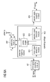
- FIG. 2 is a schematic block diagram illustrating the configuration of an antenna switching path in accordance with an embodiment of the present invention.
- the right-hand half of FIG. 2 shows the grid networking structure constituted by these antenna switching devices
- the left-hand half of FIG. 2 shows that the antenna switching device accepts the configuration from a path configuration module and is designated as a node in the antenna switching path, where a trigger may be built in the antenna switching device.
- this trigger can activate the switch function of the antenna switching device in the abovementioned embodiments, and it then joins the antenna switching procedure. In other cases, the switch function of the antenna switching device is not activated and it will not join the antenna switching procedure.
- FIG. 3 is a schematic block diagram of the operational principle of an antenna switching system in accordance this embodiment of the present invention.
- the reader sends out an RF signal in a predetermined period to control the switching of the antennae and detects the down edge of the RF signal when performing a switching, and the terminator reflects the RF signal and forms a feedback signal, and detects the up edge of the feedback signal after the reader has been switched to the last antenna.
- the whole switching procedure is as follows:
- antenna switching devices 1 , 2 and 3 are each connected to their respective antennae and are disconnected from the next hop in the forward link.
- antenna switching device 1 detects a down edge of the RF signal, then it disconnects from its respective antenna, connects to the next hop in the forward link, and sends the RF signal to the next hop, and at this moment, as shown in FIG. 3 , the reader has been connected to antenna switching device 2 , i.e., it is switched from the antenna corresponding to antenna switching device 1 to the antenna corresponding to antenna switching device 2 . 3.
- antenna switching device 2 detects a down edge of the RF signal, then it disconnects from its respective antenna, connects to the next hop in the forward link, and sends the RF signal to the next hop, and at this moment, as shown in FIG.
- antenna switching device 3 detects a down edge of the RF signal, then it disconnects from its respective antenna, connects to the next hop in the forward link, and sends the RF signal to the next hop, and at this moment, as shown in FIG. 3 , the reader has been connected to the terminator, i.e., it is switched from the antenna corresponding to antenna switching device 3 to the terminator.
- the terminator reflects a feedback signal to the backward link, and at this moment, antenna switching devices 1 , 2 and 3 are connected. 5.
- Antenna switching devices 1 , 2 and 3 detect an up edge of the feedback signal at time t 4 , and recover to the initial status, i.e., all of them connect to their respective antennae and disconnect from the next hop in the forward link.
- this embodiment of the present invention further provides an antenna switching device, the particular construction and structure and the implementing principles thereof are described below.
- FIG. 4A is a schematic block diagram of the construction and structure of an antenna switching device in accordance with an embodiment of the present invention.
- the antenna switching device in this RFID system comprises a first signal coupling module 401 , a detection triggering module 403 , and a switching module 402 , where the initial status of the switching module 402 is that it is connected to its respective antenna (i.e., J 1 and J 2 ends are connected) and disconnected from the next hop in the forward link (i.e., J 1 and J 3 ends are disconnected).
- the first signal coupling module 401 receives an RF signal from a previous hop in the forward link and outputs the RF signal to the detection triggering module 403 and the switching module 402 .
- the RF signal is a radio frequency communication signal sent out by the reader.
- the reader is switched to the next antenna (i.e., the antenna correspondingly connected to the next hop in the forward link).
- the detection triggering module 403 can comprise: a first signal detection module 501 and a control trigger 502 .
- the first signal detection module 501 is used for detecting a down edge or an up edge of the radio frequency communication signal and triggering the control trigger 502 when detecting the down edge or the up edge of the radio frequency communication signal
- the control trigger 502 is used for sending a first switching instruction to the switching module 402 when it is triggered by the first signal detection module 501 .
- the detection triggering module 403 can comprise: a first signal detection module 501 and a first timing trigger 503 .
- the first signal detection module 501 is used for triggering the first timing trigger 503 when detecting the radio frequency communication signal from the forward link
- the first timing trigger 503 is used for starting a first timer when it is triggered by the first signal detection module 501 and outputting a first switching instruction to the switching module 402 when the first timer has timed out.
- the detection triggering modules 403 shown in FIGS. 5A and 5B can both further comprise: a second timing trigger 504 .
- the first signal detection module 501 is further used for triggering the second timing trigger 504 when detecting the radio frequency communication signal from the forward link;
- the second timing trigger 504 is further used for starting a second timer when it is triggered by the first signal detection module 501 and outputting a second switching instruction to the switching module when the second timer has timed out
- the switching module 402 is further used for resetting to the initial status when it receives the second switching instruction.
- the detection triggering module 403 as shown in FIG. 5B comprises the first signal detection module 501 , the first timing trigger 503 and the second timing trigger 504 , its operational principles can also be as follows:
- the first signal detection module 501 is used for triggering the first timing trigger 503 when detecting the radio frequency communication signal from the forward link, the first timing trigger 503 is used for starting a first timer when it is triggered by the first signal detection module 501 and outputting a first switching instruction to the switching module 402 when the first timer has timed out and at the same time triggering the second timing trigger 504 ; the second timing trigger 504 is further used for starting a second timer when it is triggered by the first signal detection module 501 and outputting a second switching instruction to the switching module when the second timer has timed out, and the switching module 402 is further used for resetting to the initial status when it receives the second switching instruction.
- the detection triggering module 403 shown in FIG. 5E can be further implemented as a circuit structure shown in FIG. 5F .
- the initial status of the switching module 402 is that J 2 is connected to J 1
- the default outputs of the second timing trigger 504 and the first timing trigger 503 are both low voltages
- the timer counts by the high voltage triggering and the first signal detection module 501 is used for detecting the voltage value of a forward RF signal.
- the operational principles of the detection triggering module 403 are as follows:
- the first signal detection module 501 When the first signal detection module 501 detects the forward RF signal as a high voltage, it will trigger the first timing trigger 503 to start the first timer to count (assuming that the initial value of the first timer is T 1 ). After T 1 (the first timer having timed out), the first timing trigger 503 controls the switching module 402 via VI so as to connect J 3 to J 1 , and at the same time outputs a high voltage to the second timing trigger 504 so as to trigger it to start the second timer to count.
- the antenna connected to the switching module 402 can receive a forward RF signal from a previous hop in the forward link and then communicate with a tag. After T 1 , the switching module 402 will be connected to the antenna switching device of the next hop over the forward link and then the reader will be switched to the antenna connected to the antenna switching device of the next hop.
- the second timing trigger 504 cause the second timer to start counting when it is triggered, and when the counting begins, the output of the second timing trigger 504 changes to a high voltage.
- the initial value of the second timer is set to be T 2 (T 2 >>T 1 in the practical applications).
- the second timing trigger 504 controls the switching module 402 via V 2 to connect J 2 to J 1 , and at the same time its output changes to a low voltage that is output to an NOT gate.
- the antenna switching device will reset to the initial status, i.e., it connects to its respective antenna per se and disconnects from the next hop in the forward link.
- the first signal detection module again detects a high voltage, the abovementioned switching process will be repeated and a new cycle of switching then starts.
- FIG. 4B is a schematic block diagram of the construction and structure of an antenna switching device in accordance with an embodiment of the present invention.
- the antenna switching device in the RFID system comprises a first signal coupling module 401 , a detection triggering module 403 , a switching module 402 and a second signal coupling module 404 , in which the initial status of the switching module 402 is that it connects to its respective antenna (i.e., J 1 and J 2 ends are connected) and disconnects from the next hop in the forward link (i.e., J 1 and J 3 ends are disconnected).
- the first signal coupling module 401 receives an RF signal from a previous hop over the forward link and outputs the RF signal to the detection triggering module 403 and the switching module 402 .
- the RF signal is a radio frequency communication signal sent out by the reader.
- the reader is switched to the next antenna (i.e., the antenna correspondingly connected to the next hop in the forward link).
- the terminator When the RF signal is sent to the terminator connected to the antenna switching device that is connected to the last hop in the forward link, the terminator reflects the RF signal and forms a feedback signal and resets to the initial status using this feedback signal, and its particular resetting process is as follows:
- the second signal coupling module 404 receives the feedback signal from a previous hop over the backward link and outputs it to the detection triggering module 403 and the switching module 402 .
- the switching module 402 further outputs the feedback signal to the first signal coupling module 401 , and connects to its respective antenna (i.e., J 1 and J 2 ends are connected) when it receives the second switching instruction and disconnects from the second signal coupling module 404 (i.e., J 1 and J 3 ends are disconnected). 4.
- the first signal coupling module 401 outputs the feedback signal to a next hop in the backward link.
- the detection triggering module 403 can comprise a first signal detection module 601 , a second signal detection module 603 and a control trigger 602 .
- the first signal detection module 601 is used for detecting a down edge or an up edge of an RF signal and for triggering the control trigger 602 when detecting the down edge or the up edge of the RF signal;
- the second signal detection module 603 is used for detecting an up edge or a down edge of a feedback signal from the backward link and triggering the control trigger 602 when detecting the up edge or the down edge of the feedback signal from the backward link, and
- the control trigger 602 is used for sending a first switching instruction to the switching module 402 when it is triggered by the first signal detection module 601 and sends a second switching instruction to the switching module 402 when it is triggered by the second signal detection module 603 .
- the second signal detection module 603 can further be used for triggering the control trigger 602 or directly outputting the second switching instruction to the switching module 402 when detecting the feedback signal from the backward link.
- the detection triggering module 403 can comprise a first signal detection module 601 , a second signal detection module 603 and a first timing trigger 604 .
- the first signal detection module 601 is used for triggering the first timing trigger 604 when detecting an RF signal from the forward link
- the first timing trigger 604 is used for starting a first timer when it is triggered by the first signal detection module 601 and outputting a first switching instruction to the switching module 402 when the first timer has timed out
- the second signal detection module 603 is used for outputting a second switching instruction to the switching module 402 when detecting a feedback signal from the backward link.
- the detection triggering module 403 shown in FIG. 6B can be further implemented as a circuit structure shown in FIG. 6C .
- the initial status of the switching module 402 is that J 2 is connected to J 1
- the default output of the first timing trigger 604 is a low voltage
- the timer counts by the high voltage triggering and the first signal detection module 601 is used for detecting the voltage value of a forward RF signal
- the second signal detection module 602 is used for detecting the voltage value of the feedback signal, with the default outputs of both being low voltages.
- This detection triggering module 403 The operational principles of this detection triggering module 403 are as follows:
- the first signal detection module 601 When the first signal detection module 601 detects the forward RF signal as a high voltage, it will trigger the first timing trigger 604 to start the first timer to begin counting (assuming that the initial value of the first timer is T 1 ). After T 1 (the first timer having timed out), the first timing trigger 604 controls the switching module 402 via V 1 to connect J 3 to J 1 . At the same time, the first timing trigger 604 triggers the second signal detection module to output a high voltage. Within T 1 , the antenna connected to the switching module 402 can receive the forward RF signal from the previous hop over the forward link and then communicate with a tag. After T 1 , the switching module 402 will be connected to the antenna switching device of the next hop over the forward link and the reader will then be switched to the antenna connected to the antenna switching device of the next hop.
- the switching modules corresponding to all the antennae are set to be connected to a next hop over the forward link, and at this moment, the RF signal will be reflected by a terminator to form a feedback signal.
- the second signal detection module 602 will be used to detect the voltage of the feedback signal, and if the feedback signal is detected to be a high voltage, then the second signal detection module 602 is changed to output a low voltage. At this moment, the switching module 402 will reset to the initial status.
- the first signal detection module 601 detects a high voltage again, the abovementioned switching process will be repeated and then a new run of switching starts.
- the detection triggering module 403 can further comprise a first signal detection module, a second signal detection module, a first timing trigger and a control trigger, where the first signal detection module is used for triggering the first timing trigger when detecting the radio frequency communication signal from the forward link, the first timing trigger is used for starting a first timer when it is triggered by the first signal detection module and outputting a first switching instruction to the switching module when the first timer has timed out, the second signal detection module is used for detecting an up edge or a down edge of a feedback signal from the backward link and triggering the control trigger when detecting the up edge or the down edge of the feedback signal, and when the control trigger is used for outputting a second switching instruction to the switching module when it is triggered by the second signal detection module.
- the first signal detection module is used for triggering the first timing trigger when detecting the radio frequency communication signal from the forward link
- the first timing trigger is used for starting a first timer when it is triggered by the first signal detection module and outputting a first switching instruction to the switching
- a preset tag when the reader outputs continuous RF signals to communicate with a tag, a preset tag can be built in the antenna to determine at the antenna of which hop the read tag is read, so that the reader can estimate from which antenna the preset tag is read according to the time interval of reading the preset tag and the set parameters of the timer (e.g., T 1 and T 2 ).
- the abovementioned antenna switching devices can further comprise a path configuration module for accepting a configuration so as to add an antenna switching device into an antenna switching path.
- the antenna switching path comprises each of the antenna switching devices involved in the sequential switching, and when an antenna switching device is added into this antenna switching path, the abovementioned functions related to the antenna switching of the antenna switching device will be activated, thus enabling the antenna switching device to join the switching process of this antenna switching path.
- the detection triggering module 403 (or the control triggers 502 and 602 and the timing triggers 503 , 504 , and 604 therein) in the antenna switching device provided by the abovementioned embodiments of the present invention needs a certain operating voltage to ensure its normal operation.
- This contemplated embodiment of the present invention provides two antenna switching devices employing different ways for supplying the operation voltages: one is an active one and the other is a passive one.
- the antenna switching device is a passive and further comprises a charge pump for receiving a radio frequency communication signal from a previous hop in the forward link and for providing an operating voltage to the detection triggering module.
- FIG. 7A is a schematic block diagram of the construction and structure of an active antenna switching device in accordance with this embodiment of the present invention.
- the operating voltage of each antenna switching device is provided by a direct-current (DC) power supply provided by the reader via RF cables, and the antenna switching device is as shown in FIG. 4B .
- the antenna switching device receives an RF signal and a direct current (DC) from the RF cables, and the antenna switching device shown in FIG. 4B needs to add two interconnected biasing devices: a first biasing device 701 and a second biasing device 702 .
- the first biasing device 701 splits the RF signal and DC from the RF cables into two routes, with one route being RF signal and the other being DC, where the RF signal is output to the first signal coupling module 401 and DC is output to the detection triggering module 403 (or the control trigger 602 and the timing trigger 604 ).
- the first biasing device 701 and the second biasing device 702 are connected to each other.
- the second biasing device 702 is able to combine the RF signal from the second signal coupling module 404 and the DC from the first biasing device 701 into one route of signal (RF signal+DC) to transmit over the RF cables.
- FIG. 7B is a schematic block diagram of the construction and structure of an active antenna switching device in accordance with an embodiment of the present invention.
- the operating voltage of each antenna switching device is provided by a direct-current (DC) power supply provided by the reader via RF cables, and the antenna switching device employs the implementation as shown in FIG. 4A .
- the antenna switching device receives an RF signal and a direct-current (DC) from the RF cables, and the antenna switching device shown in FIG. 4A needs to add two interconnected biasing devices, i.e., a first biasing device 701 and a second biasing device 702 .
- the first biasing device 701 splits the RF signal and DC from the RF cables into two routes, with one route being RF signal and the other being DC, where the RF signal is output to the first signal coupling module 401 and DC is output to the detection triggering module 403 (or the control trigger 502 and the timing triggers 503 , 504 ).
- the first biasing device 701 and the second biasing device 702 are connected to each other.
- the second biasing device 702 is able to combine the RF signal from the switching module 402 and the DC from the first biasing device 701 into one route of signal (RF signal+DC) to transmit over the RF cables.
- FIG. 8 is a schematic block diagram of the construction and structure of a passive antenna switching device in accordance with an embodiment of the present invention.
- a charge pump is built in the antenna switching device, and the operating voltage can be automatically provided to the detection triggering module 403 (or the control triggers 502 , 602 and the timing triggers 503 , 504 , 604 therein) depending on the RF signals over the RF cables.
- the antenna switching device receives an RF signal from the RF cables, and this RF signal is also input into a charge pump 801 apart from being input into the first signal coupling module 401 , and this charge pump 801 then processes this RF signal so as to provide an operating voltage to the detection triggering module 403 .
- the antenna switching device employs the implementation shown in FIG. 4B , and when the antenna switching device employs the implementation shown in FIG. 4A , the connection manner and operational principles of the charge pump 801 do not change, which will not be presented in the accompanying drawings.
- the first signal detection modules 501 and 601 when the first signal detection modules 501 and 601 are used for detecting the down edge or the up edge of a radio frequency communication signal, the first signal detection modules 501 and 601 can comprise an envelope detection module, a differential circuit and a time delay module, where the enveloping detection module is used for obtaining the envelope of the radio frequency communication signal from the first signal coupling module, the differential circuit is used for processing the envelope of the radio frequency communication signal from the envelope detection module so as to detect the down edge or the up edges in the envelope, and the time delay module is used for performing a time delay processing to the output of the differential circuit and then triggering the control trigger.
- the enveloping detection module is used for obtaining the envelope of the radio frequency communication signal from the first signal coupling module
- the differential circuit is used for processing the envelope of the radio frequency communication signal from the envelope detection module so as to detect the down edge or the up edges in the envelope
- the time delay module is used for performing a time delay processing to the output of the differential circuit and then triggering the
- the second signal detection module 603 can comprise an envelope detection module and a differential circuit, where the envelope detection module is used for obtaining the envelope of the feedback signal from a second signal coupling module, the differential circuit is used for processing the envelope of the feedback signal from the envelope detection module so as to detect the down edge or the up edge in the envelope and then triggering the control trigger, and where the first signal coupling module 401 and the second signal coupling module 404 can be directional couplers, the first biasing device 701 and the second biasing device 702 can be bias tees, and the charge pump 801 can be an AC/DC charge pump.
- the structures of the antenna switching device provided by this embodiment of the present invention are as shown in FIGS. 9 and 10 .
- FIG. 9 is a schematic block diagram of the construction and structure of a passive antenna switching device in accordance with an embodiment of the present invention.
- the first signal detection module 601 comprises an envelope detection module 901 , a differential circuit 902 and a time delay module 903
- the second signal detection module 603 comprises an envelope detection module 904 and a differential circuit 905
- the first signal coupling module 401 and the second signal coupling module 404 are both directional couplers (a two-directional coupler is employed here) and the charge pump 801 is an AC/DC charge pump.
- the envelope detection modules 901 and 905 can obtain the envelope of an RF signal according to an inputted RF signal (such as a radio frequency communication signal or a feedback signal), the differential circuits 902 and 904 can process the envelope from the envelope detection module 901 or 905 so as to detect an up edge or a down edge in this envelope, therefore it can trigger the control trigger 602 when detecting the up edge or the down edge of this envelope, and the time delay module 903 can perform a time delay processing to the processed results from the differential circuit 902 .
- an inputted RF signal such as a radio frequency communication signal or a feedback signal
- the differential circuits 902 and 904 can process the envelope from the envelope detection module 901 or 905 so as to detect an up edge or a down edge in this envelope, therefore it can trigger the control trigger 602 when detecting the up edge or the down edge of this envelope
- the time delay module 903 can perform a time delay processing to the processed results from the differential circuit 902 .
- FIG. 10 is a schematic block diagram of the construction and structure of an active antenna switching device in accordance with an embodiment of the present invention. As shown in FIG. 10 , the difference between this active antenna switching device and the passive antenna switching device shown in FIG. 9 is that it comprises a first biasing device 701 and a second biasing device 702 , both of which are bias tees, but it does not comprise the AC/DC charge pump 801 .
- FIG. 11 shows a schematic diagram of a reader providing a power supply voltage to an active antenna switching device in accordance with this embodiment of the present invention.
- the original part of the reader outputs an RF signal to a biasing device (a bias tee is employed here) and the additive DC power supply of the reader also outputs DC to the bias tee, which bias tee combines these two routes of signals into one route of signal (RF signal+DC) to output to the antenna switching device.
- a bias tee is employed here
- the additive DC power supply of the reader also outputs DC to the bias tee, which bias tee combines these two routes of signals into one route of signal (RF signal+DC) to output to the antenna switching device.
- the particular implementation of the differential circuit and charge pump employed by the antenna switching device can be implemented in a traditional way and they can also employ other designs, and no restrictions thereto are made in the present invention.
- FIG. 12 is a schematic block diagram of the differential circuit employed by an antenna switching device according to an embodiment of the present invention.
- U 1 is the input voltage of the differential circuit
- U 2 is the output voltage of the differential circuit
- the control trigger can be used to detect the up edges or down edges in the envelope.
- FIG. 13 is a schematic block diagram of an alternating/direct current (AC-DC) charge pump employed by the antenna switching device in accordance with an embodiment of the present invention. It can be seen from FIG. 13 that the alternating/direct current charge pump can output an operating voltage (V dd ) to the control trigger after having the inputted RF signal processed.
- AC-DC alternating/direct current
- the contemplated embodiment of the present invention further provides an antenna system in an RFID system, which comprises an antenna and an antenna switching device disposed outside the antenna and an antenna in an RFID system, with an antenna switching device being built in this antenna.
- this antenna switching device can be any of the abovementioned embodiments, and the operational principles of which will not be described redundantly here.
- this embodiment of the present invention further provides a method for addressing antennae in an RFID system, which method comprises successively switching a reader to some of or all of the antennae in a plurality of antennae according to a radio frequency communication signal from the reader so as to address an antenna therein. For example, if there is a total of four antenna in the system and it needs to address the third antenna, then the reader can be successively switched from the first antenna to the third antenna by sending out a periodical radio frequency communication signal, i.e., addressing the third antenna.
- the antenna addressing method is as follows: designating an antenna to be addressed by designating the number of periods of the radio frequency communication signal, and switching the reader to the next antenna in each period, and when the radio frequency communication signal sends out a designated number of periods, the antenna to which the reader is switched would be the one to be addressed. For example, if the third antenna is to be addressed, a radio frequency communication signal with two periods can be sent out in succession, then the reader will be switched to the third antenna in the second period, i.e. the third antenna is now addressed.
- the reader can be switched to the next one of the antennae when detecting a down edge or an up edge of the radio frequency communication signal, and the particular switching principles have been described in detail above, and will not be repeated here.
- the wiring facilities in the RFID system-based smart shelves system can be greatly simplified, the difficulty in forming a network will be reduced significantly and the workload of the construction workers will also be reduced.
- the embodiments of the present invention have considerable technical effects in terms of wiring facilities, costs of implementation, etc.
- the embodiments of the present invention do not introduce any change to the software and hardware of the reader.
- Ordinary antennae can also be used directly in disclosed embodiments of the present invention.
- the disclosed embodiments of the present invention do not depend on any specific signals over cables to operate. Therefore, it is easy to implement the embodiments of the present invention in combination with existing systems.
- the design of a passive antenna switching device provided by the disclosed embodiments of the present invention removes the needs for DC power supply, and when employing such passive antenna switching devices, the costs of the whole system can be further reduced significantly.
Abstract
Description
(ii). a reader, which is used for reading/writing the information stored in the tag and can be hand-held or fixed, in which case there is generally one reader included in an RFID system, which reader reads the information stored in each tag (sometimes it can even write the tag information into a tag) so as to achieve the control, detection or tracking of the item to which a tag is attached, and the reader can also be referred to herein as an interrogator; and
(iii). an antenna, which is disposed on the reader and is used for transmitting a radio-frequency signal between each tag and the reader so as to transmit information between the reader and the tag.
2. When the radio frequency communication signal is sent out continuously or sent out in a predetermined period, the reader can be switched to a next one of the antennae every once in a while by setting a timer. Particularly, the treatment regarding each of the antennae comprises starting a first timer when an antenna or an antenna switching device corresponding to the antenna detects a radio frequency communication signal, and switching the reader to a next one of the antennae when the first timer is timed out. Such a switching method by setting a timer does not limit the way for the transmission of the radio frequency communication signal, and this method can be employed either for the radio frequency communication signals sent out continuously or the one sent out periodically. In this case, the method for detecting a radio frequency communication signal can be as follows: detecting whether the strength of the radio frequency communication signal meets a predetermined condition (for example, with the power, or the amplitude of the radio frequency communication signal reaching predetermined thresholds), and when the detected strength of the radio frequency communication signal meets the predetermined condition, it is considered that a radio frequency communication signal has been detected.
2. When the radio frequency communication signal is sent out in a predetermined period or sent out continuously, the reader can be re-switched to the antenna adjacent thereto at the time when the feedback signal is detected. In this case, the method for detecting the feedback signal can be as follows: detecting whether the strength of the feedback signal meets a predetermined condition (for example, with the power or the amplitude of the feedback signal reaching predetermined thresholds), and when the detected strength of the feedback signal meets the predetermined condition, it is considered that a feedback signal is detected.
2. When the radio frequency communication signal is sent out in a predetermined period or sent out continuously, the antenna switching device starts a first timer when detecting a down edge or an up edge of the radio frequency communication signal, disconnects from its respective antenna and connects to the next hop in the forward link when the first timer is timeout, and outputs the radio frequency communication signal to the next hop in the forward link.
2. When the radio frequency communication signal is sent out in a predetermined period or sent out continuously, the antenna switching device connects to its respective antenna and disconnects from the previous hop in the backward link when it detects a feedback signal and outputs the feedback signal to the next hop in the backward link.
3. At time t2,
4. At time t3,
5.
2. The
3. The
2. The
3. The
4. The first
Claims (19)
Applications Claiming Priority (4)
| Application Number | Priority Date | Filing Date | Title |
|---|---|---|---|
| CN201010163139 | 2010-04-30 | ||
| CN201010163139.X | 2010-04-30 | ||
| CN201010163139.XA CN102236772B (en) | 2010-04-30 | 2010-04-30 | Antenna switching method, device and system and antenna addressing method in radio frequency identification (RFID) system |
| PCT/EP2011/055498 WO2011134772A1 (en) | 2010-04-30 | 2011-04-08 | Radio frequency shield with proximity change alert for a contactless data carrier |
Publications (2)
| Publication Number | Publication Date |
|---|---|
| US20130210356A1 US20130210356A1 (en) | 2013-08-15 |
| US9166657B2 true US9166657B2 (en) | 2015-10-20 |
Family
ID=44170254
Family Applications (1)
| Application Number | Title | Priority Date | Filing Date |
|---|---|---|---|
| US13/695,472 Expired - Fee Related US9166657B2 (en) | 2010-04-30 | 2011-04-08 | Radio frequency shield with proximity change alert for a contactless data carrier |
Country Status (4)
| Country | Link |
|---|---|
| US (1) | US9166657B2 (en) |
| EP (1) | EP2564348B1 (en) |
| CN (1) | CN102236772B (en) |
| WO (1) | WO2011134772A1 (en) |
Families Citing this family (6)
| Publication number | Priority date | Publication date | Assignee | Title |
|---|---|---|---|---|
| CN103914714B (en) * | 2012-12-31 | 2017-03-01 | 西门子公司 | For the initialized system of electronic tag |
| CN103400166B (en) * | 2013-07-31 | 2016-06-22 | 中国科学院自动化研究所 | A kind of closing space-intensive Articla management system based on RFID and method |
| CN104318275A (en) * | 2014-09-26 | 2015-01-28 | 杭州中瑞思创科技股份有限公司 | Ultra-high-frequency reader-writer antenna extension method and intelligent antenna splitter based on frame length switching channels |
| US9954749B2 (en) * | 2015-03-17 | 2018-04-24 | Getac Technology Corporation | Detection circuit and detecting method thereof |
| EP3713014A1 (en) * | 2019-03-21 | 2020-09-23 | Nokia Solutions and Networks Oy | Configurable antenna arrangements |
| CN111711919B (en) * | 2020-05-26 | 2022-06-10 | 桃芯科技(苏州)有限公司 | Method, electronic device, and computer storage medium for controlling antenna timing switching |
Citations (5)
| Publication number | Priority date | Publication date | Assignee | Title |
|---|---|---|---|---|
| CN1834982A (en) | 2005-03-18 | 2006-09-20 | 富士通株式会社 | Antenna switching equipment |
| US20060267777A1 (en) * | 1999-08-09 | 2006-11-30 | Micron Technology, Inc. | RFID material tracking method and apparatus |
| WO2008012856A2 (en) | 2006-07-27 | 2008-01-31 | Entropia S.R. S.R.L. | Rfid network for tracking documents and goods |
| US20090284354A1 (en) | 2008-05-19 | 2009-11-19 | Sirit Technologies Inc. | Multiplexing Radio Frequency Signals |
| US20100007471A1 (en) * | 2007-03-27 | 2010-01-14 | Brother Kogyo Kabushiki Kaisha | Apparatus for reading RFID tag |
-
2010
- 2010-04-30 CN CN201010163139.XA patent/CN102236772B/en not_active Expired - Fee Related
-
2011
- 2011-04-08 EP EP11714734.8A patent/EP2564348B1/en not_active Not-in-force
- 2011-04-08 WO PCT/EP2011/055498 patent/WO2011134772A1/en active Application Filing
- 2011-04-08 US US13/695,472 patent/US9166657B2/en not_active Expired - Fee Related
Patent Citations (6)
| Publication number | Priority date | Publication date | Assignee | Title |
|---|---|---|---|---|
| US20060267777A1 (en) * | 1999-08-09 | 2006-11-30 | Micron Technology, Inc. | RFID material tracking method and apparatus |
| CN1834982A (en) | 2005-03-18 | 2006-09-20 | 富士通株式会社 | Antenna switching equipment |
| US20060220870A1 (en) | 2005-03-18 | 2006-10-05 | Fujitsu Limited | Antenna switching equipment |
| WO2008012856A2 (en) | 2006-07-27 | 2008-01-31 | Entropia S.R. S.R.L. | Rfid network for tracking documents and goods |
| US20100007471A1 (en) * | 2007-03-27 | 2010-01-14 | Brother Kogyo Kabushiki Kaisha | Apparatus for reading RFID tag |
| US20090284354A1 (en) | 2008-05-19 | 2009-11-19 | Sirit Technologies Inc. | Multiplexing Radio Frequency Signals |
Also Published As
| Publication number | Publication date |
|---|---|
| EP2564348A1 (en) | 2013-03-06 |
| CN102236772B (en) | 2014-07-02 |
| WO2011134772A1 (en) | 2011-11-03 |
| EP2564348B1 (en) | 2016-01-20 |
| CN102236772A (en) | 2011-11-09 |
| US20130210356A1 (en) | 2013-08-15 |
Similar Documents
| Publication | Publication Date | Title |
|---|---|---|
| US9166657B2 (en) | Radio frequency shield with proximity change alert for a contactless data carrier | |
| CN101859392B (en) | Radio frequency identification reader | |
| US8497762B2 (en) | Network control | |
| US8941471B2 (en) | RF switched RFID multiplexer | |
| JP5068122B2 (en) | RFID system | |
| US20120139712A1 (en) | Hybrid switch for extending antenna port and method of controlling the same, and rfid system using the hybrid switch | |
| US20090303007A1 (en) | Multiple band rfid reader device | |
| US8350676B2 (en) | System and method for allowing multiple RFID reader devices to read RFID tags without collision | |
| CN101226581B (en) | Electronic label array and system for separation multiplexing of chip and antenna as well as implementing method | |
| CN103577857A (en) | RFID three-dimensional detecting device and use method thereof | |
| WO2013163809A1 (en) | Rfid system, reader in rfid system, addressing method for antenna in rfid system and cascaded antennas in rfid system | |
| US8981907B1 (en) | RFID antenna multiplexing | |
| CN112418377B (en) | Electronic price tag and working method thereof | |
| WO2021019021A1 (en) | Rfid integrated light infrastructure | |
| CN114118330B (en) | Integrated radio frequency identification integrated circuit and radio frequency identification code providing method | |
| CN203573337U (en) | RFID three-dimensional detection device | |
| AU2012204104B9 (en) | Network control | |
| JP2011501329A (en) | RFID network control and redundancy | |
| JP2017073692A (en) | Wireless tag, pallet, pallet management device, and pallet management system | |
| CN102938083A (en) | Data machine room behavior tracking method and system based on RFID (Radio Frequency Identification) | |
| CN103854034A (en) | Radio frequency identification reader control method | |
| CN101398909B (en) | Method and device for obtaining Btree branch tree number, responder and responsion method | |
| CN103634357A (en) | Radio frequency identification controller and radio frequency identification system, and controlling method of radio frequency identification reader |
Legal Events
| Date | Code | Title | Description |
|---|---|---|---|
| AS | Assignment |
Owner name: SIEMENS AKTIENGESELLSCHAFT, GERMANY Free format text: ASSIGNMENT OF ASSIGNORS INTEREST;ASSIGNORS:LAMPE, MATTHIAS;YU, DAN;YUAN, YONG;SIGNING DATES FROM 20121105 TO 20121109;REEL/FRAME:029593/0818 |
|
| FEPP | Fee payment procedure |
Free format text: PAYOR NUMBER ASSIGNED (ORIGINAL EVENT CODE: ASPN); ENTITY STATUS OF PATENT OWNER: LARGE ENTITY |
|
| STCF | Information on status: patent grant |
Free format text: PATENTED CASE |
|
| MAFP | Maintenance fee payment |
Free format text: PAYMENT OF MAINTENANCE FEE, 4TH YEAR, LARGE ENTITY (ORIGINAL EVENT CODE: M1551); ENTITY STATUS OF PATENT OWNER: LARGE ENTITY Year of fee payment: 4 |
|
| FEPP | Fee payment procedure |
Free format text: MAINTENANCE FEE REMINDER MAILED (ORIGINAL EVENT CODE: REM.); ENTITY STATUS OF PATENT OWNER: LARGE ENTITY |
|
| LAPS | Lapse for failure to pay maintenance fees |
Free format text: PATENT EXPIRED FOR FAILURE TO PAY MAINTENANCE FEES (ORIGINAL EVENT CODE: EXP.); ENTITY STATUS OF PATENT OWNER: LARGE ENTITY |
|
| STCH | Information on status: patent discontinuation |
Free format text: PATENT EXPIRED DUE TO NONPAYMENT OF MAINTENANCE FEES UNDER 37 CFR 1.362 |
|
| FP | Lapsed due to failure to pay maintenance fee |
Effective date: 20231020 |