US9166175B2 - Organic electroluminescent materials and devices - Google Patents
Organic electroluminescent materials and devices Download PDFInfo
- Publication number
- US9166175B2 US9166175B2 US13/686,763 US201213686763A US9166175B2 US 9166175 B2 US9166175 B2 US 9166175B2 US 201213686763 A US201213686763 A US 201213686763A US 9166175 B2 US9166175 B2 US 9166175B2
- Authority
- US
- United States
- Prior art keywords
- group
- aryl
- organic light
- alkyl
- sulfanyl
- Prior art date
- Legal status (The legal status is an assumption and is not a legal conclusion. Google has not performed a legal analysis and makes no representation as to the accuracy of the status listed.)
- Active, expires
Links
- 0 C*c1nc2ccccc2[n]1-c1ccccc1 Chemical compound C*c1nc2ccccc2[n]1-c1ccccc1 0.000 description 23
- NSXJEEMTGWMJPY-UHFFFAOYSA-N C1=CC(N2C3=C(C=CC=C3)C3=C2C=CC=C3)=CC(C2=CC=CC(N3C4=C(C=CC=C4)C4=C3C=CC=C4)=C2)=C1 Chemical compound C1=CC(N2C3=C(C=CC=C3)C3=C2C=CC=C3)=CC(C2=CC=CC(N3C4=C(C=CC=C4)C4=C3C=CC=C4)=C2)=C1 NSXJEEMTGWMJPY-UHFFFAOYSA-N 0.000 description 3
- MZYDBGLUVPLRKR-UHFFFAOYSA-N C1=CC(N2C3=C(C=CC=C3)C3=C2C=CC=C3)=CC(N2C3=C(C=CC=C3)C3=C2C=CC=C3)=C1 Chemical compound C1=CC(N2C3=C(C=CC=C3)C3=C2C=CC=C3)=CC(N2C3=C(C=CC=C3)C3=C2C=CC=C3)=C1 MZYDBGLUVPLRKR-UHFFFAOYSA-N 0.000 description 3
- BCVMKVYCYQPIPT-UHFFFAOYSA-N C1=CC2=C(C=C1)C1=C(C=NC=C1)C1=C2C=CC=C1.C1=CC2=C(C=C1)C1=C(N=CC=C1)C1=C2C=CC=C1.C1=CC2=C(C=C1)C1=C(N=CC=C1)C1=C2C=CC=N1.C1=CC2=C(C=C1)C1=C(OC=N1)C1=C2C=CC=C1.C1=CC2=C(C=C1)OC=N2.C1=CC2=C(N=C1)N=CO2.C1=CC2=CN=CN=C2C=C1.C1=CC2=NC=CN=C2C=C1.C1=CC=C(N2C=NC3=C2C=CC=C3)C=C1.C1=CC=C(N2C=NN=C2)C=C1.C1=CC=NC=C1.C1=CN=CC=N1.C1=CN=CN=C1.C1=NC=NC=N1.C1=NN=CO1 Chemical compound C1=CC2=C(C=C1)C1=C(C=NC=C1)C1=C2C=CC=C1.C1=CC2=C(C=C1)C1=C(N=CC=C1)C1=C2C=CC=C1.C1=CC2=C(C=C1)C1=C(N=CC=C1)C1=C2C=CC=N1.C1=CC2=C(C=C1)C1=C(OC=N1)C1=C2C=CC=C1.C1=CC2=C(C=C1)OC=N2.C1=CC2=C(N=C1)N=CO2.C1=CC2=CN=CN=C2C=C1.C1=CC2=NC=CN=C2C=C1.C1=CC=C(N2C=NC3=C2C=CC=C3)C=C1.C1=CC=C(N2C=NN=C2)C=C1.C1=CC=NC=C1.C1=CN=CC=N1.C1=CN=CN=C1.C1=NC=NC=N1.C1=NN=CO1 BCVMKVYCYQPIPT-UHFFFAOYSA-N 0.000 description 3
- CWOXEPTUGKHFFJ-UHFFFAOYSA-N CC(C)(C)C1=CC(C2=CC=CC=C2)=NC(C2=CC=CC=C2)=N1.CC(C)(C)C1=CC=C(C2=NC(C3=CC=CC=C3)=CC(C3=CC=CC=C3)=N2)C=C1.CC(C)(C)C1=CC=C(C2=NC(C3=CC=CC=C3)=NC(C3=CC=CC=C3)=N2)C=C1.CC(C)(C)C1=NC(C2=CC=CC=C2)=CC(C2=CC=CC=C2)=N1.CC(C)(C)C1=NC(C2=CC=CC=C2)=NC(C2=CC=CC=C2)=N1 Chemical compound CC(C)(C)C1=CC(C2=CC=CC=C2)=NC(C2=CC=CC=C2)=N1.CC(C)(C)C1=CC=C(C2=NC(C3=CC=CC=C3)=CC(C3=CC=CC=C3)=N2)C=C1.CC(C)(C)C1=CC=C(C2=NC(C3=CC=CC=C3)=NC(C3=CC=CC=C3)=N2)C=C1.CC(C)(C)C1=NC(C2=CC=CC=C2)=CC(C2=CC=CC=C2)=N1.CC(C)(C)C1=NC(C2=CC=CC=C2)=NC(C2=CC=CC=C2)=N1 CWOXEPTUGKHFFJ-UHFFFAOYSA-N 0.000 description 3
- OQRQMFCMBCLSFL-UHFFFAOYSA-N CC(C)(C)C1=CC=C(C2=CC(C3=CC=CC=C3)=NC(C3=CC=CC=C3)=N2)C=C1.CC(C)(C)C1=CC=C(C2=NC3=C(C=CC=C3)N2C2=CC=CC=C2)C=C1.CC(C)(C)C1=CC=C2/C=C\C=C/C2=N1.CC(C)(C)C1=CC=C2/C=C\C=C/C2=N1.CC(C)(C)C1=NC2=C(C=CC=C2)N1C1=CC=CC=C1 Chemical compound CC(C)(C)C1=CC=C(C2=CC(C3=CC=CC=C3)=NC(C3=CC=CC=C3)=N2)C=C1.CC(C)(C)C1=CC=C(C2=NC3=C(C=CC=C3)N2C2=CC=CC=C2)C=C1.CC(C)(C)C1=CC=C2/C=C\C=C/C2=N1.CC(C)(C)C1=CC=C2/C=C\C=C/C2=N1.CC(C)(C)C1=NC2=C(C=CC=C2)N1C1=CC=CC=C1 OQRQMFCMBCLSFL-UHFFFAOYSA-N 0.000 description 3
- ATMNEOAHALWGQU-UHFFFAOYSA-N CC(C)(C)C1=NC2=C(C=C1)C1=C(/C=C\C=C/1)C1=C2C=CC=C1.CC(C)(C)C1=NC2=C(C=C1)C1=C(/C=C\C=C/1)C1=C2N=CC=C1.CC(C)(C)C1=NC2=C(O1)C1=C(C=CC=C1)C1=C2C=CC=C1 Chemical compound CC(C)(C)C1=NC2=C(C=C1)C1=C(/C=C\C=C/1)C1=C2C=CC=C1.CC(C)(C)C1=NC2=C(C=C1)C1=C(/C=C\C=C/1)C1=C2N=CC=C1.CC(C)(C)C1=NC2=C(O1)C1=C(C=CC=C1)C1=C2C=CC=C1 ATMNEOAHALWGQU-UHFFFAOYSA-N 0.000 description 3
- RJURWGQJLSZCIF-UHFFFAOYSA-N CC(C)(C)N1C2=C(/C=C\C=C/2)C2=CC=C3C4=CC=CC=C4CC3=C21.CC(C)(C)N1C2=C(C=C(C3=CC=CC=C3)C=C2)C2=CC=C3C4=CC=CC=C4CC3=C21.CC(C)(C)N1C2=C(C=CC=C2)C2=CC=C3C4=CC=CC(C5=CC=CC=C5)=C4CC3=C21.CC(C)(C)N1C2=C(C=CC=C2)C2=CC=C3CC4=C(C=CC=C4)C3=C21.CC(C)(C)N1C2=CC3=C(C=C2C2=C1/C=C\C=C/2)CC1=C3C=CC=C1.CC(C)(C)N1C2=CC=C3CC4=CC=CC=C4C3=C2C2=C1/C=C\C=C/2.CC(C)C1=C2CC3=C4C(=CC=C3C2=CC=C1)C1=C(C=CC=C1)N4C(C)(C)C Chemical compound CC(C)(C)N1C2=C(/C=C\C=C/2)C2=CC=C3C4=CC=CC=C4CC3=C21.CC(C)(C)N1C2=C(C=C(C3=CC=CC=C3)C=C2)C2=CC=C3C4=CC=CC=C4CC3=C21.CC(C)(C)N1C2=C(C=CC=C2)C2=CC=C3C4=CC=CC(C5=CC=CC=C5)=C4CC3=C21.CC(C)(C)N1C2=C(C=CC=C2)C2=CC=C3CC4=C(C=CC=C4)C3=C21.CC(C)(C)N1C2=CC3=C(C=C2C2=C1/C=C\C=C/2)CC1=C3C=CC=C1.CC(C)(C)N1C2=CC=C3CC4=CC=CC=C4C3=C2C2=C1/C=C\C=C/2.CC(C)C1=C2CC3=C4C(=CC=C3C2=CC=C1)C1=C(C=CC=C1)N4C(C)(C)C RJURWGQJLSZCIF-UHFFFAOYSA-N 0.000 description 3
- LCYUPYMMLQEKRC-UHFFFAOYSA-N CC(C)(C)N1C2=CC3=C(C=C2C2=C1/C=C\C=C/2)C1=CC=CC=C1C3.CC(C)(C)N1C2=CC=C3C4=C(C=CC=C4)CC3=C2C2=C1/C=C\C(C1=CC=CC=C1)=C/2.CC(C)(C)N1C2=CC=C3C4=C(C=CC=C4)CC3=C2C2=C1/C=C\C=C/2.CC(C)(C)N1C2=CC=C3C4=C(CC3=C2C2=C1/C=C\C=C/2)C(C1=CC=CC=C1)=CC=C4.CC(C)C1=CC=CC2=C1CC1=C3C(=CC=C21)N(C(C)(C)C)C1=C3/C=C\C=C/1 Chemical compound CC(C)(C)N1C2=CC3=C(C=C2C2=C1/C=C\C=C/2)C1=CC=CC=C1C3.CC(C)(C)N1C2=CC=C3C4=C(C=CC=C4)CC3=C2C2=C1/C=C\C(C1=CC=CC=C1)=C/2.CC(C)(C)N1C2=CC=C3C4=C(C=CC=C4)CC3=C2C2=C1/C=C\C=C/2.CC(C)(C)N1C2=CC=C3C4=C(CC3=C2C2=C1/C=C\C=C/2)C(C1=CC=CC=C1)=CC=C4.CC(C)C1=CC=CC2=C1CC1=C3C(=CC=C21)N(C(C)(C)C)C1=C3/C=C\C=C/1 LCYUPYMMLQEKRC-UHFFFAOYSA-N 0.000 description 3
- CCCOZNVPFKBJLV-UHFFFAOYSA-N C.C.C1=CC2=C(C=C1)C1=C(N=CC1)C1=C2C=CC=C1.C1=CC2=C(C=C1)N=CC2 Chemical compound C.C.C1=CC2=C(C=C1)C1=C(N=CC1)C1=C2C=CC=C1.C1=CC2=C(C=C1)N=CC2 CCCOZNVPFKBJLV-UHFFFAOYSA-N 0.000 description 2
- NBVQXQAREBJTSP-UHFFFAOYSA-N C.C1=CC=CC=C1.C1=CCC=C1 Chemical compound C.C1=CC=CC=C1.C1=CCC=C1 NBVQXQAREBJTSP-UHFFFAOYSA-N 0.000 description 2
- QKVWPNRUXZYLQV-UHFFFAOYSA-N C1=CC(C2=C/C=C3\C4=C(C=CC=C4)C4=C(C=CC=C4)\C3=C\2)=CC(C2=CC=CC3=C2SC2=C3C=CC=C2)=C1 Chemical compound C1=CC(C2=C/C=C3\C4=C(C=CC=C4)C4=C(C=CC=C4)\C3=C\2)=CC(C2=CC=CC3=C2SC2=C3C=CC=C2)=C1 QKVWPNRUXZYLQV-UHFFFAOYSA-N 0.000 description 2
- VFUDMQLBKNMONU-UHFFFAOYSA-N C1=CC2=C(C=C1)N(C1=CC=C(C3=CC=C(N4C5=C(C=CC=C5)C5=C4C=CC=C5)C=C3)C=C1)C1=C2C=CC=C1 Chemical compound C1=CC2=C(C=C1)N(C1=CC=C(C3=CC=C(N4C5=C(C=CC=C5)C5=C4C=CC=C5)C=C3)C=C1)C1=C2C=CC=C1 VFUDMQLBKNMONU-UHFFFAOYSA-N 0.000 description 2
- SDEFDICGRVDKPH-UHFFFAOYSA-M C1=CC2=C3C(=C1)O[AlH]/N3=C/C=C\2 Chemical compound C1=CC2=C3C(=C1)O[AlH]/N3=C/C=C\2 SDEFDICGRVDKPH-UHFFFAOYSA-M 0.000 description 2
- VEPGVVSQFKYADF-UHFFFAOYSA-N C1=CC=C(C2=CC3=C(C=C2)N(C2=CC=C(C4=NC(C5=CC=CC=C5)=NC(C5=CC=CC=C5)=N4)C=C2)C2=C4SC5=CC=CC=C5C4=CC=C32)C=C1.C1=CC=C(C2=NC(C3=CC=CC=C3)=NC(C3=CC=C(N4C5=C(C=CC=C5)C5=CC=C6C7=CC=CC(C8=CC=CC=C8)=C7SC6=C54)C=C3)=N2)C=C1.C1=CC=C(C2=NC(C3=CC=CC=C3)=NC(C3=CC=C(N4C5=C(C=CC=C5)C5=C\C=C6\C7=CC=CC=C7S\C6=C\54)C=C3)=N2)C=C1 Chemical compound C1=CC=C(C2=CC3=C(C=C2)N(C2=CC=C(C4=NC(C5=CC=CC=C5)=NC(C5=CC=CC=C5)=N4)C=C2)C2=C4SC5=CC=CC=C5C4=CC=C32)C=C1.C1=CC=C(C2=NC(C3=CC=CC=C3)=NC(C3=CC=C(N4C5=C(C=CC=C5)C5=CC=C6C7=CC=CC(C8=CC=CC=C8)=C7SC6=C54)C=C3)=N2)C=C1.C1=CC=C(C2=NC(C3=CC=CC=C3)=NC(C3=CC=C(N4C5=C(C=CC=C5)C5=C\C=C6\C7=CC=CC=C7S\C6=C\54)C=C3)=N2)C=C1 VEPGVVSQFKYADF-UHFFFAOYSA-N 0.000 description 2
- WGBPHKISRLSIPB-UHFFFAOYSA-N C1=CC=C(C2=CC3=C(C=C2)N(C2=CC=C(C4=NC(C5=CC=CC=C5)=NC(C5=CC=CC=C5)=N4)C=C2)C2=CC=C4C5=C(C=CC=C5)SC4=C23)C=C1.C1=CC=C(C2=NC(C3=CC=CC=C3)=NC(C3=CC=C(N4C5=CC6=C(C=C5C5=C4C=CC=C5)C4=CC=CC=C4S6)C=C3)=N2)C=C1.CC(C)C1=CC=CC2=C1SC1=C3C(=CC=C21)N(C1=CC=C(C2=NC(C4=CC=CC=C4)=NC(C4=CC=CC=C4)=N2)C=C1)C1=C3C=CC=C1 Chemical compound C1=CC=C(C2=CC3=C(C=C2)N(C2=CC=C(C4=NC(C5=CC=CC=C5)=NC(C5=CC=CC=C5)=N4)C=C2)C2=CC=C4C5=C(C=CC=C5)SC4=C23)C=C1.C1=CC=C(C2=NC(C3=CC=CC=C3)=NC(C3=CC=C(N4C5=CC6=C(C=C5C5=C4C=CC=C5)C4=CC=CC=C4S6)C=C3)=N2)C=C1.CC(C)C1=CC=CC2=C1SC1=C3C(=CC=C21)N(C1=CC=C(C2=NC(C4=CC=CC=C4)=NC(C4=CC=CC=C4)=N2)C=C1)C1=C3C=CC=C1 WGBPHKISRLSIPB-UHFFFAOYSA-N 0.000 description 2
- NWJVMDIZAIGZNV-UHFFFAOYSA-N C1=CC=C(C2=CC3=C(C=C2)N(C2=NC(C4=CC=CC=C4)=NC(C4=CC=CC=C4)=N2)C2=C4SC5=CC=CC=C5C4=CC=C32)C=C1.C1=CC=C(C2=NC(C3=CC=CC=C3)=NC(N3C4=CC5=C(C=C4C4=C3C=CC=C4)SC3=C5C=CC=C3)=N2)C=C1.C1=CC=C(C2=NC(C3=CC=CC=C3)=NC(N3C4=CC=C5SC6=CC=CC=C6C5=C4C4=C3C=CC=C4)=N2)C=C1.CC(C)C1=C2SC3=C4C(=CC=C3C2=CC=C1)C1=C(C=CC=C1)N4C1=NC(C2=CC=CC=C2)=NC(C2=CC=CC=C2)=N1 Chemical compound C1=CC=C(C2=CC3=C(C=C2)N(C2=NC(C4=CC=CC=C4)=NC(C4=CC=CC=C4)=N2)C2=C4SC5=CC=CC=C5C4=CC=C32)C=C1.C1=CC=C(C2=NC(C3=CC=CC=C3)=NC(N3C4=CC5=C(C=C4C4=C3C=CC=C4)SC3=C5C=CC=C3)=N2)C=C1.C1=CC=C(C2=NC(C3=CC=CC=C3)=NC(N3C4=CC=C5SC6=CC=CC=C6C5=C4C4=C3C=CC=C4)=N2)C=C1.CC(C)C1=C2SC3=C4C(=CC=C3C2=CC=C1)C1=C(C=CC=C1)N4C1=NC(C2=CC=CC=C2)=NC(C2=CC=CC=C2)=N1 NWJVMDIZAIGZNV-UHFFFAOYSA-N 0.000 description 2
- RTHSPXNNVVXQSD-UHFFFAOYSA-N C1=CC=C(C2=CC3=C(C=C2)N(C2=NC(C4=CC=CC=C4)=NC(C4=CC=CC=C4)=N2)C2=CC=C4C5=C(C=CC=C5)SC4=C23)C=C1.C1=CC=C(C2=CC=CC3=C2SC2=C4C(=CC=C32)N(C2=NC(C3=CC=CC=C3)=NC(C3=CC=CC=C3)=N2)C2=C4C=CC=C2)C=C1.C1=CC=C(C2=NC(C3=CC=CC=C3)=NC(N3C4=CC=C5C6=C(C=CC=C6)SC5=C4C4=C3C=CC=C4)=N2)C=C1 Chemical compound C1=CC=C(C2=CC3=C(C=C2)N(C2=NC(C4=CC=CC=C4)=NC(C4=CC=CC=C4)=N2)C2=CC=C4C5=C(C=CC=C5)SC4=C23)C=C1.C1=CC=C(C2=CC=CC3=C2SC2=C4C(=CC=C32)N(C2=NC(C3=CC=CC=C3)=NC(C3=CC=CC=C3)=N2)C2=C4C=CC=C2)C=C1.C1=CC=C(C2=NC(C3=CC=CC=C3)=NC(N3C4=CC=C5C6=C(C=CC=C6)SC5=C4C4=C3C=CC=C4)=N2)C=C1 RTHSPXNNVVXQSD-UHFFFAOYSA-N 0.000 description 2
- GYQQGPYPWLHRQV-UHFFFAOYSA-N C1=CC=C(C2=CC=CC3=C2SC2=C4C(=CC=C32)N(C2=CC=C(C3=NC(C5=CC=CC=C5)=NC(C5=CC=CC=C5)=N3)C=C2)C2=C4C=CC=C2)C=C1.C1=CC=C(C2=NC(C3=CC=CC=C3)=NC(C3=CC=C(N4C5=CC=C6C7=C(C=CC=C7)SC6=C5C5=C4C=CC=C5)C=C3)=N2)C=C1.C1=CC=C(C2=NC(C3=CC=CC=C3)=NC(N3C4=C(C=CC=C4)C4=CC=C5SC6=C(C=CC=C6)C5=C43)=N2)C=C1 Chemical compound C1=CC=C(C2=CC=CC3=C2SC2=C4C(=CC=C32)N(C2=CC=C(C3=NC(C5=CC=CC=C5)=NC(C5=CC=CC=C5)=N3)C=C2)C2=C4C=CC=C2)C=C1.C1=CC=C(C2=NC(C3=CC=CC=C3)=NC(C3=CC=C(N4C5=CC=C6C7=C(C=CC=C7)SC6=C5C5=C4C=CC=C5)C=C3)=N2)C=C1.C1=CC=C(C2=NC(C3=CC=CC=C3)=NC(N3C4=C(C=CC=C4)C4=CC=C5SC6=C(C=CC=C6)C5=C43)=N2)C=C1 GYQQGPYPWLHRQV-UHFFFAOYSA-N 0.000 description 2
- DHDHJYNTEFLIHY-UHFFFAOYSA-N C1=CC=C(C2=CC=NC3=C2C=CC2=C3N=CC=C2C2=CC=CC=C2)C=C1 Chemical compound C1=CC=C(C2=CC=NC3=C2C=CC2=C3N=CC=C2C2=CC=CC=C2)C=C1 DHDHJYNTEFLIHY-UHFFFAOYSA-N 0.000 description 2
- ZIQCLCREYZRGBW-UHFFFAOYSA-N C1=CC=C(C2=NC(C3=CC=CC=C3)=NC(C3=CC=C(N4C5=CC6=C(C=C5C5=C4C=CC=C5)SC4=C6C=CC=C4)C=C3)=N2)C=C1.CC(C)C1=C2SC3=C4C(=CC=C3C2=CC=C1)C1=C(C=CC=C1)N4C1=CC=C(C2=NC(C3=CC=CC=C3)=NC(C3=CC=CC=C3)=N2)C=C1 Chemical compound C1=CC=C(C2=NC(C3=CC=CC=C3)=NC(C3=CC=C(N4C5=CC6=C(C=C5C5=C4C=CC=C5)SC4=C6C=CC=C4)C=C3)=N2)C=C1.CC(C)C1=C2SC3=C4C(=CC=C3C2=CC=C1)C1=C(C=CC=C1)N4C1=CC=C(C2=NC(C3=CC=CC=C3)=NC(C3=CC=CC=C3)=N2)C=C1 ZIQCLCREYZRGBW-UHFFFAOYSA-N 0.000 description 2
- HPZXLHPEQLRGNM-UHFFFAOYSA-N C1=CC=C(C2=NC(C3=CC=CC=C3)=NC(N3C4=C(C=CC=C4)C4=CC=C5C6=C(C=CC=C6)SC5=C43)=N2)C=C1 Chemical compound C1=CC=C(C2=NC(C3=CC=CC=C3)=NC(N3C4=C(C=CC=C4)C4=CC=C5C6=C(C=CC=C6)SC5=C43)=N2)C=C1 HPZXLHPEQLRGNM-UHFFFAOYSA-N 0.000 description 2
- YLKXWQDJBMEZDN-UHFFFAOYSA-N C1=CC=C(C2=NC(C3=CC=CC=C3)=NC(N3C4=C(C=CC=C4)C4=CC=C5C6=CC=CC(C7=CC=CC=C7)=C6SC5=C43)=N2)C=C1.C1=CC=C(C2=NC(C3=CC=CC=C3)=NC(N3C4=C(C=CC=C4)C4=CC=C5C6=CC=CC=C6SC5=C43)=N2)C=C1.C1=CC=C(C2=NC(C3=CC=CC=C3)=NC(N3C4=CC5=C(C=C4C4=C3C=CC=C4)C3=CC=CC=C3S5)=N2)C=C1.CC(C)C1=CC=CC2=C1SC1=C3C(=CC=C21)N(C1=NC(C2=CC=CC=C2)=NC(C2=CC=CC=C2)=N1)C1=C3C=CC=C1 Chemical compound C1=CC=C(C2=NC(C3=CC=CC=C3)=NC(N3C4=C(C=CC=C4)C4=CC=C5C6=CC=CC(C7=CC=CC=C7)=C6SC5=C43)=N2)C=C1.C1=CC=C(C2=NC(C3=CC=CC=C3)=NC(N3C4=C(C=CC=C4)C4=CC=C5C6=CC=CC=C6SC5=C43)=N2)C=C1.C1=CC=C(C2=NC(C3=CC=CC=C3)=NC(N3C4=CC5=C(C=C4C4=C3C=CC=C4)C3=CC=CC=C3S5)=N2)C=C1.CC(C)C1=CC=CC2=C1SC1=C3C(=CC=C21)N(C1=NC(C2=CC=CC=C2)=NC(C2=CC=CC=C2)=N1)C1=C3C=CC=C1 YLKXWQDJBMEZDN-UHFFFAOYSA-N 0.000 description 2
- IBHBKWKFFTZAHE-UHFFFAOYSA-N C1=CC=C(N(C2=CC=C(C3=CC=C(N(C4=CC=CC=C4)C4=C5C=CC=CC5=CC=C4)C=C3)C=C2)C2=CC=CC3=C2C=CC=C3)C=C1 Chemical compound C1=CC=C(N(C2=CC=C(C3=CC=C(N(C4=CC=CC=C4)C4=C5C=CC=CC5=CC=C4)C=C3)C=C2)C2=CC=CC3=C2C=CC=C3)C=C1 IBHBKWKFFTZAHE-UHFFFAOYSA-N 0.000 description 2
- CRHRWHRNQKPUPO-UHFFFAOYSA-N C1=CC=C(N(C2=CC=C(N(C3=CC=C(N(C4=CC=CC=C4)C4=C5C=CC=CC5=CC=C4)C=C3)C3=CC=C(N(C4=CC=CC=C4)C4=C5C=CC=CC5=CC=C4)C=C3)C=C2)C2=C3C=CC=CC3=CC=C2)C=C1 Chemical compound C1=CC=C(N(C2=CC=C(N(C3=CC=C(N(C4=CC=CC=C4)C4=C5C=CC=CC5=CC=C4)C=C3)C3=CC=C(N(C4=CC=CC=C4)C4=C5C=CC=CC5=CC=C4)C=C3)C=C2)C2=C3C=CC=CC3=CC=C2)C=C1 CRHRWHRNQKPUPO-UHFFFAOYSA-N 0.000 description 2
- GEQBRULPNIVQPP-UHFFFAOYSA-N C1=CC=C(N2C(C3=CC(/C4=N/C5=C(C=CC=C5)N4C4=CC=CC=C4)=CC(/C4=N/C5=C(C=CC=C5)N4C4=CC=CC=C4)=C3)=NC3=C2C=CC=C3)C=C1 Chemical compound C1=CC=C(N2C(C3=CC(/C4=N/C5=C(C=CC=C5)N4C4=CC=CC=C4)=CC(/C4=N/C5=C(C=CC=C5)N4C4=CC=CC=C4)=C3)=NC3=C2C=CC=C3)C=C1 GEQBRULPNIVQPP-UHFFFAOYSA-N 0.000 description 2
- FIRNXGIHIBWXDV-UHFFFAOYSA-N CC(C)(C1=CC=C(N2C3=C(C=CC=C3)C3=C2C=CC=N3)C=C1)C1=CC=C(C(C)(C)C2=CC=C(N3C4=C(C=CC=C4)C4=C3C=CC=N4)C=C2)C=C1 Chemical compound CC(C)(C1=CC=C(N2C3=C(C=CC=C3)C3=C2C=CC=N3)C=C1)C1=CC=C(C(C)(C)C2=CC=C(N3C4=C(C=CC=C4)C4=C3C=CC=N4)C=C2)C=C1 FIRNXGIHIBWXDV-UHFFFAOYSA-N 0.000 description 2
- NNPPMTNAJDCUHE-UHFFFAOYSA-N CC(C)C Chemical compound CC(C)C NNPPMTNAJDCUHE-UHFFFAOYSA-N 0.000 description 2
- XYYYIVRDTLXJEF-UHFFFAOYSA-L CC1=N2/C3=C(C=CC=C3O[Al]2OC2=CC=C(C3=CC=CC=C3)C=C2)/C=C\1 Chemical compound CC1=N2/C3=C(C=CC=C3O[Al]2OC2=CC=C(C3=CC=CC=C3)C=C2)/C=C\1 XYYYIVRDTLXJEF-UHFFFAOYSA-L 0.000 description 2
- STTGYIUESPWXOW-UHFFFAOYSA-N CC1=NC2=C(C=CC3=C2N=C(C)C=C3C2=CC=CC=C2)C(C2=CC=CC=C2)=C1 Chemical compound CC1=NC2=C(C=CC3=C2N=C(C)C=C3C2=CC=CC=C2)C(C2=CC=CC=C2)=C1 STTGYIUESPWXOW-UHFFFAOYSA-N 0.000 description 2
- FFZAGEJIUNEDGO-UHFFFAOYSA-N CN1C2=C(C=CC=C2)N2C3=CC=CC4=C3[Os](C12)C1N(C)C2=C(C=CC=C2)N41 Chemical compound CN1C2=C(C=CC=C2)N2C3=CC=CC4=C3[Os](C12)C1N(C)C2=C(C=CC=C2)N41 FFZAGEJIUNEDGO-UHFFFAOYSA-N 0.000 description 2
- AYOMISFIGMZTGF-UHFFFAOYSA-O BrC1=CC=C(N(C2=CC=C([NH+](C3=C4C=CC=CC4=C4C=CC=CC4=C3)C3=C4C=CC=CC4=C4C=CC=CC4=C3)C=C2)C2=C3C=CC=CC3=C3C=CC=CC3=C2)C=C1 Chemical compound BrC1=CC=C(N(C2=CC=C([NH+](C3=C4C=CC=CC4=C4C=CC=CC4=C3)C3=C4C=CC=CC4=C4C=CC=CC4=C3)C=C2)C2=C3C=CC=CC3=C3C=CC=CC3=C2)C=C1 AYOMISFIGMZTGF-UHFFFAOYSA-O 0.000 description 1
- FSZHBEYFUBAVJU-UHFFFAOYSA-N C(#C[Au]12C3=CC=CC=C3C3=CC=CC(=N31)C1=CC=CC=C12)C1=CC=C(N(C2=CC=CC=C2)C2=CC=CC=C2)C=C1 Chemical compound C(#C[Au]12C3=CC=CC=C3C3=CC=CC(=N31)C1=CC=CC=C12)C1=CC=C(N(C2=CC=CC=C2)C2=CC=CC=C2)C=C1 FSZHBEYFUBAVJU-UHFFFAOYSA-N 0.000 description 1
- RVNWTQIBASUOPP-UHFFFAOYSA-N C.C.C.CCC Chemical compound C.C.C.CCC RVNWTQIBASUOPP-UHFFFAOYSA-N 0.000 description 1
- JXENMZIPSCWUBC-UHFFFAOYSA-N C.C1=CC=N2[Ir]N3=C(C=CC=C3)C2=C1 Chemical compound C.C1=CC=N2[Ir]N3=C(C=CC=C3)C2=C1 JXENMZIPSCWUBC-UHFFFAOYSA-N 0.000 description 1
- PFELVPQDPVRECH-UHFFFAOYSA-N C1=CB2C3=N(C=CC=C3)[Ir]N2C=C1 Chemical compound C1=CB2C3=N(C=CC=C3)[Ir]N2C=C1 PFELVPQDPVRECH-UHFFFAOYSA-N 0.000 description 1
- FEEVDOPOKYHDKB-UHFFFAOYSA-N C1=CC(C2=CC3=C(C=C2)C2=C(C=CC=C2)C2=C3C=CC=C2)=CC(C2=CC3=C(C=C2)C2=C(C=CC=C2)C2=C3C=CC=C2)=C1 Chemical compound C1=CC(C2=CC3=C(C=C2)C2=C(C=CC=C2)C2=C3C=CC=C2)=CC(C2=CC3=C(C=C2)C2=C(C=CC=C2)C2=C3C=CC=C2)=C1 FEEVDOPOKYHDKB-UHFFFAOYSA-N 0.000 description 1
- ZGEUUNNIQMDTKF-UHFFFAOYSA-N C1=CC(C2=CC3=C(C=C2)OC2=C3C=C(N3C4=C(C=CC=C4)C4=C3C=CC=C4)C=C2)=CC(C2=CC=C3OC4=C(C=C(N5C6=C(C=CC=C6)C6=C5C=CC=C6)C=C4)C3=C2)=C1 Chemical compound C1=CC(C2=CC3=C(C=C2)OC2=C3C=C(N3C4=C(C=CC=C4)C4=C3C=CC=C4)C=C2)=CC(C2=CC=C3OC4=C(C=C(N5C6=C(C=CC=C6)C6=C5C=CC=C6)C=C4)C3=C2)=C1 ZGEUUNNIQMDTKF-UHFFFAOYSA-N 0.000 description 1
- IMKXSEPQICZHSL-UHFFFAOYSA-N C1=CC(C2=CC3=C(C=C2)SC2=C3C=CC=C2)=CC(C2=CC(N3C4=C(C=CC=C4)C4=C3C=CC=C4)=CC=C2)=C1 Chemical compound C1=CC(C2=CC3=C(C=C2)SC2=C3C=CC=C2)=CC(C2=CC(N3C4=C(C=CC=C4)C4=C3C=CC=C4)=CC=C2)=C1 IMKXSEPQICZHSL-UHFFFAOYSA-N 0.000 description 1
- JXPNARCIEUVCJY-UHFFFAOYSA-N C1=CC(C2=CC=CC(C3=CC(C4=CC(C5=CN=CC=C5)=CC=C4)=CC(C4=CC(C5=CN=CC=C5)=CC=C4)=C3)=C2)=CN=C1.C1=CC=C([Si](C2=CC=CC=C2)(C2=CC=CC3=C2SC2=C3/C=C\C=C/2)/C2=C/C=C\C3=C2SC2=C3C=CC=C2)C=C1.CC1=CC=C(N(C2=CC=C(C)C=C2)C2=CC=C(C3(C4=CC=C(N(C5=CC=C(C)C=C5)C5=CC=C(C)C=C5)C=C4)CCCCC3)C=C2)C=C1 Chemical compound C1=CC(C2=CC=CC(C3=CC(C4=CC(C5=CN=CC=C5)=CC=C4)=CC(C4=CC(C5=CN=CC=C5)=CC=C4)=C3)=C2)=CN=C1.C1=CC=C([Si](C2=CC=CC=C2)(C2=CC=CC3=C2SC2=C3/C=C\C=C/2)/C2=C/C=C\C3=C2SC2=C3C=CC=C2)C=C1.CC1=CC=C(N(C2=CC=C(C)C=C2)C2=CC=C(C3(C4=CC=C(N(C5=CC=C(C)C=C5)C5=CC=C(C)C=C5)C=C4)CCCCC3)C=C2)C=C1 JXPNARCIEUVCJY-UHFFFAOYSA-N 0.000 description 1
- KFKHNBPNJMWUEG-UHFFFAOYSA-N C1=CC(C2=CC=CC(C3=CC4=C(C=C3)C3=C(C=CC=C3)C3=C4C=CC=C3)=C2)=CC(C2=CC3=C(C=C2)C2=C(C=CC=C2)C2=C3C=CC=C2)=C1 Chemical compound C1=CC(C2=CC=CC(C3=CC4=C(C=C3)C3=C(C=CC=C3)C3=C4C=CC=C3)=C2)=CC(C2=CC3=C(C=C2)C2=C(C=CC=C2)C2=C3C=CC=C2)=C1 KFKHNBPNJMWUEG-UHFFFAOYSA-N 0.000 description 1
- IHUZMIYPBUPXCM-UHFFFAOYSA-N C1=CC2=C(C=C1)C1=C(/C=C\C(N3C4=C(C=CC=C4)C4=C3/C=C/C(N3C5=C(C=CC=C5)C5=C3/C=C\C=C/5)=C\4)=C/1)S2 Chemical compound C1=CC2=C(C=C1)C1=C(/C=C\C(N3C4=C(C=CC=C4)C4=C3/C=C/C(N3C5=C(C=CC=C5)C5=C3/C=C\C=C/5)=C\4)=C/1)S2 IHUZMIYPBUPXCM-UHFFFAOYSA-N 0.000 description 1
- VLLWEJLXGZPRBP-UHFFFAOYSA-N C1=CC2=C(C=C1)C1=C(/C=C\C=C/1)C2.C1=CC2=C(C=C1)C1=C(/C=C\C=C/1)C2.C1=CC2=C3C=CC=CC3=C3/C=C\C=C/C3=C2C=C1.C1=CC2=CC=C3/C=C\C=C/C3=C2C=C1.C1=CC=C(C2=CC=CC(C3=CC=CC=C3)=C2)C=C1.C1=CC=C2C=C3C=CC=CC3=CC2=C1.C1=CC=C2C=CC=CC2=C1.CC1=CC=C(C)C=C1 Chemical compound C1=CC2=C(C=C1)C1=C(/C=C\C=C/1)C2.C1=CC2=C(C=C1)C1=C(/C=C\C=C/1)C2.C1=CC2=C3C=CC=CC3=C3/C=C\C=C/C3=C2C=C1.C1=CC2=CC=C3/C=C\C=C/C3=C2C=C1.C1=CC=C(C2=CC=CC(C3=CC=CC=C3)=C2)C=C1.C1=CC=C2C=C3C=CC=CC3=CC2=C1.C1=CC=C2C=CC=CC2=C1.CC1=CC=C(C)C=C1 VLLWEJLXGZPRBP-UHFFFAOYSA-N 0.000 description 1
- OQVRQHSMSFIVDA-UHFFFAOYSA-N C1=CC2=C(C=C1)C1=C(C2)C2=C(C=C1)CC1=C2C=CC=C1.C1=CC2=C(C=C1)C1=C(C=CC3=C1C1=C(/C=C\C=C/1)C3)C2.C1=CC2=C(C=C1)C1=CC3=C(C=C1C2)C1=C(/C=C\C=C/1)C3.C1=CC2=C(C=C1)C1=CC3=C(C=C1C2)CC1=C3/C=C\C=C/1 Chemical compound C1=CC2=C(C=C1)C1=C(C2)C2=C(C=C1)CC1=C2C=CC=C1.C1=CC2=C(C=C1)C1=C(C=CC3=C1C1=C(/C=C\C=C/1)C3)C2.C1=CC2=C(C=C1)C1=CC3=C(C=C1C2)C1=C(/C=C\C=C/1)C3.C1=CC2=C(C=C1)C1=CC3=C(C=C1C2)CC1=C3/C=C\C=C/1 OQVRQHSMSFIVDA-UHFFFAOYSA-N 0.000 description 1
- BAGADZFHGISJHX-UHFFFAOYSA-N C1=CC2=C(C=C1)C1=C(N=CC1)C1=C2C=CC=C1.C1=CC2=C(C=C1)N=CC2 Chemical compound C1=CC2=C(C=C1)C1=C(N=CC1)C1=C2C=CC=C1.C1=CC2=C(C=C1)N=CC2 BAGADZFHGISJHX-UHFFFAOYSA-N 0.000 description 1
- HSPZYQUMRCQDDG-UHFFFAOYSA-N C1=CC2=C(C=C1)C1=CC=C3[Ir]N4=C(C=CC=C4)C3=C1S2 Chemical compound C1=CC2=C(C=C1)C1=CC=C3[Ir]N4=C(C=CC=C4)C3=C1S2 HSPZYQUMRCQDDG-UHFFFAOYSA-N 0.000 description 1
- SDHNJSIZTIODFW-UHFFFAOYSA-N C1=CC2=C(C=C1)N(C1=CC3=C(C=C1)SC1=C3/C=C(N3C4=C(C=CC=C4)C4=C3C=CC=C4)\C=C/1)C1=C2C=CC=C1 Chemical compound C1=CC2=C(C=C1)N(C1=CC3=C(C=C1)SC1=C3/C=C(N3C4=C(C=CC=C4)C4=C3C=CC=C4)\C=C/1)C1=C2C=CC=C1 SDHNJSIZTIODFW-UHFFFAOYSA-N 0.000 description 1
- UHPYEWCZOHAIEP-UHFFFAOYSA-N C1=CC2=C(C=C1)N(C1=CC3=C(N=C1)OC1=C3/C=C(N3C4=C(C=CC=C4)C4=C3C=CC=C4)\C=C/1)C1=C2C=CC=C1 Chemical compound C1=CC2=C(C=C1)N(C1=CC3=C(N=C1)OC1=C3/C=C(N3C4=C(C=CC=C4)C4=C3C=CC=C4)\C=C/1)C1=C2C=CC=C1 UHPYEWCZOHAIEP-UHFFFAOYSA-N 0.000 description 1
- AWXGSYPUMWKTBR-UHFFFAOYSA-N C1=CC2=C(C=C1)N(C1=CC=C(N(C3=CC=C(N4C5=C(C=CC=C5)C5=C4C=CC=C5)C=C3)C3=CC=C(N4C5=C(C=CC=C5)C5=C4/C=C\C=C/5)C=C3)C=C1)C1=C2C=CC=C1 Chemical compound C1=CC2=C(C=C1)N(C1=CC=C(N(C3=CC=C(N4C5=C(C=CC=C5)C5=C4C=CC=C5)C=C3)C3=CC=C(N4C5=C(C=CC=C5)C5=C4/C=C\C=C/5)C=C3)C=C1)C1=C2C=CC=C1 AWXGSYPUMWKTBR-UHFFFAOYSA-N 0.000 description 1
- CQZOLIZFWRSNOM-UHFFFAOYSA-N C1=CC2=C(C=C1)N1CC3=CC=CC4=C3[Ir]35(C6=CN(CC7=CC=CC(=N73)CN3C=C5C5=C3C=CC=C5)C3=C6C=CC=C3)(N1=C2)N1=CC2=C(C=CC=C2)N1C4 Chemical compound C1=CC2=C(C=C1)N1CC3=CC=CC4=C3[Ir]35(C6=CN(CC7=CC=CC(=N73)CN3C=C5C5=C3C=CC=C5)C3=C6C=CC=C3)(N1=C2)N1=CC2=C(C=CC=C2)N1C4 CQZOLIZFWRSNOM-UHFFFAOYSA-N 0.000 description 1
- VDRONIBNVZLDJL-UHFFFAOYSA-N C1=CC2=C(SC3=C2/C=C\C=C/3N2C3=C(C=CC=C3)C3=C2C=CC=C3)C(N2C3=C(C=CC=C3)C3=C2C=CC=C3)=C1 Chemical compound C1=CC2=C(SC3=C2/C=C\C=C/3N2C3=C(C=CC=C3)C3=C2C=CC=C3)C(N2C3=C(C=CC=C3)C3=C2C=CC=C3)=C1 VDRONIBNVZLDJL-UHFFFAOYSA-N 0.000 description 1
- KSUVCAUJLZAQFV-UHFFFAOYSA-N C1=CC2=C3C(=C1)C1=C(C=CC=C1)N1/C(C4=C(C5CCCCC5)C=CC=C4C4CCCCC4)=C\N(=C\31)[Ir]2 Chemical compound C1=CC2=C3C(=C1)C1=C(C=CC=C1)N1/C(C4=C(C5CCCCC5)C=CC=C4C4CCCCC4)=C\N(=C\31)[Ir]2 KSUVCAUJLZAQFV-UHFFFAOYSA-N 0.000 description 1
- YIEVUWKWEWXJAD-UHFFFAOYSA-N C1=CC2=C3C(=C1)CN1C=CN4CC5=C6C(=CC=C5)CN5C=CN(C2)C5[Pt]36C14 Chemical compound C1=CC2=C3C(=C1)CN1C=CN4CC5=C6C(=CC=C5)CN5C=CN(C2)C5[Pt]36C14 YIEVUWKWEWXJAD-UHFFFAOYSA-N 0.000 description 1
- UZNKNEKOAXWFOI-UHFFFAOYSA-N C1=CC2=C3C(=C1)[Ir]N1=C3N(C=C1)/C=C\2 Chemical compound C1=CC2=C3C(=C1)[Ir]N1=C3N(C=C1)/C=C\2 UZNKNEKOAXWFOI-UHFFFAOYSA-N 0.000 description 1
- SBYMPPVIXIJQGA-UHFFFAOYSA-N C1=CC2=C3C4=C1C1=C5C4=C4C6=C\3C3=C2C=CC2=C3/C3=C\6C6=C4/C4=C5/C(=C5/C=C\C7=C8C=CC2=C3C8=C/6/C7=C/54)/C=C\1 Chemical compound C1=CC2=C3C4=C1C1=C5C4=C4C6=C\3C3=C2C=CC2=C3/C3=C\6C6=C4/C4=C5/C(=C5/C=C\C7=C8C=CC2=C3C8=C/6/C7=C/54)/C=C\1 SBYMPPVIXIJQGA-UHFFFAOYSA-N 0.000 description 1
- PCWKWGNZYZSYBS-UHFFFAOYSA-M C1=CC2=C3C=CC=CC3=C3/C=C\C=C/C3=C2C=C1.C1=CC2=CC=C3/C=C\C=N/C3=C2N=C1.C1=CC=C(N2C=NC3=C2C=CC=C3)C=C1.CC1=C(F)C(F)=C(C)C(F)=C1F.C[Al](N)O.O=S1(=O)C2=C(C=CC=C2)CC2=C1C=CC=C2 Chemical compound C1=CC2=C3C=CC=CC3=C3/C=C\C=C/C3=C2C=C1.C1=CC2=CC=C3/C=C\C=N/C3=C2N=C1.C1=CC=C(N2C=NC3=C2C=CC=C3)C=C1.CC1=C(F)C(F)=C(C)C(F)=C1F.C[Al](N)O.O=S1(=O)C2=C(C=CC=C2)CC2=C1C=CC=C2 PCWKWGNZYZSYBS-UHFFFAOYSA-M 0.000 description 1
- LABGHJUTWCOYQE-UHFFFAOYSA-N C1=CC2=CC=C(C3=CC4=C(C=C3)C=C(C3=CC=CC(C5=C6C=CC=CC6=C6C=CC=CC6=C5)=C3)C=C4)C=C2C=C1 Chemical compound C1=CC2=CC=C(C3=CC4=C(C=C3)C=C(C3=CC=CC(C5=C6C=CC=CC6=C6C=CC=CC6=C5)=C3)C=C4)C=C2C=C1 LABGHJUTWCOYQE-UHFFFAOYSA-N 0.000 description 1
- ZMNZPEPFEJPQJE-UHFFFAOYSA-N C1=CC2=CC=C(C3=CC=C(C4=C5C=CC=CC5=C5/C=C(/C6=CC=C(C7=CC=C8C=CC=CC8=C7)C=C6)C6=C(C=CC=C6)C5=C4)C=C3)C=C2C=C1 Chemical compound C1=CC2=CC=C(C3=CC=C(C4=C5C=CC=CC5=C5/C=C(/C6=CC=C(C7=CC=C8C=CC=CC8=C7)C=C6)C6=C(C=CC=C6)C5=C4)C=C3)C=C2C=C1 ZMNZPEPFEJPQJE-UHFFFAOYSA-N 0.000 description 1
- IZKKEYIPFTVWHN-UHFFFAOYSA-N C1=CC2=N(C=C1)[Ir]N1N=CC=C21 Chemical compound C1=CC2=N(C=C1)[Ir]N1N=CC=C21 IZKKEYIPFTVWHN-UHFFFAOYSA-N 0.000 description 1
- MKZDOOLFFBQAOV-UHFFFAOYSA-N C1=CC2=N(C=C1)[Os]N1N=CC=C21.C1=CC=C(P(C2=CC=CC=C2)C2=CC=CC=C2)C=C1 Chemical compound C1=CC2=N(C=C1)[Os]N1N=CC=C21.C1=CC=C(P(C2=CC=CC=C2)C2=CC=CC=C2)C=C1 MKZDOOLFFBQAOV-UHFFFAOYSA-N 0.000 description 1
- LOANKKZXVZMPBA-UHFFFAOYSA-N C1=CC=C(C2=CC3=C(C=C2)[Ir]N2=CC=CN32)C=C1 Chemical compound C1=CC=C(C2=CC3=C(C=C2)[Ir]N2=CC=CN32)C=C1 LOANKKZXVZMPBA-UHFFFAOYSA-N 0.000 description 1
- RSWOJEDGRFCGFR-UHFFFAOYSA-N C1=CC=C(C2=CC3=C(C=C2C2=CC=CC=C2)C2=C(/C=C(C4=CC=CC=C4)\C(C4=CC=CC=C4)=C/2)C2=C3C=C(C3=CC=CC=C3)C(C3=CC=CC=C3)=C2)C=C1 Chemical compound C1=CC=C(C2=CC3=C(C=C2C2=CC=CC=C2)C2=C(/C=C(C4=CC=CC=C4)\C(C4=CC=CC=C4)=C/2)C2=C3C=C(C3=CC=CC=C3)C(C3=CC=CC=C3)=C2)C=C1 RSWOJEDGRFCGFR-UHFFFAOYSA-N 0.000 description 1
- WXAIEIRYBSKHDP-UHFFFAOYSA-N C1=CC=C(C2=CC=C(N(C3=CC=C(C4=CC=CC=C4)C=C3)C3=CC=C(C4=CC=C(N(C5=CC=C(C6=CC=CC=C6)C=C5)C5=CC=C(C6=CC=CC=C6)C=C5)C=C4)C=C3)C=C2)C=C1 Chemical compound C1=CC=C(C2=CC=C(N(C3=CC=C(C4=CC=CC=C4)C=C3)C3=CC=C(C4=CC=C(N(C5=CC=C(C6=CC=CC=C6)C=C5)C5=CC=C(C6=CC=CC=C6)C=C5)C=C4)C=C3)C=C2)C=C1 WXAIEIRYBSKHDP-UHFFFAOYSA-N 0.000 description 1
- KQCREFMBDCFFGP-UHFFFAOYSA-N C1=CC=C(C2=CC=C(N(C3=CC=CC=C3)C3=CC=C(C4=CC=C(N(C5=CC=CC=C5)C5=CC=C(C6=CC=C(C7=CC=C(N(C8=CC=CC=C8)C8=CC=C(C9=CC=C(N(C%10=CC=CC=C%10)C%10=CC=C(C%11=CC=CC=C%11)C=C%10)C=C9)C=C8)C=C7)C=C6)C=C5)C=C4)C=C3)C=C2)C=C1 Chemical compound C1=CC=C(C2=CC=C(N(C3=CC=CC=C3)C3=CC=C(C4=CC=C(N(C5=CC=CC=C5)C5=CC=C(C6=CC=C(C7=CC=C(N(C8=CC=CC=C8)C8=CC=C(C9=CC=C(N(C%10=CC=CC=C%10)C%10=CC=C(C%11=CC=CC=C%11)C=C%10)C=C9)C=C8)C=C7)C=C6)C=C5)C=C4)C=C3)C=C2)C=C1 KQCREFMBDCFFGP-UHFFFAOYSA-N 0.000 description 1
- UAPMHVCFJJOFBP-UHFFFAOYSA-N C1=CC=C(C2=CC=C3[Ir]N4=C(C=CC=C4)C3=C2)C=C1 Chemical compound C1=CC=C(C2=CC=C3[Ir]N4=C(C=CC=C4)C3=C2)C=C1 UAPMHVCFJJOFBP-UHFFFAOYSA-N 0.000 description 1
- MJOIBSPUXNMHKC-UHFFFAOYSA-N C1=CC=C(C2=CC=CC(C3=CC4=C(C=C3)OC3=CC5=C(C=C34)C3=C(C=CC(C4=CC=CC(C6=CC=CC=C6)=C4)=C3)O5)=C2)C=C1 Chemical compound C1=CC=C(C2=CC=CC(C3=CC4=C(C=C3)OC3=CC5=C(C=C34)C3=C(C=CC(C4=CC=CC(C6=CC=CC=C6)=C4)=C3)O5)=C2)C=C1 MJOIBSPUXNMHKC-UHFFFAOYSA-N 0.000 description 1
- HTNRLCWDKMRUIH-UHFFFAOYSA-N C1=CC=C(C2=CC=N3C4=C2/C=C\C2=C(C5=CC=CC=C5)C=CN(=C24)[Pt]3(C2=CC=CC=C2)C2=CC=CC=C2)C=C1.CF.CF.FF.FF.FF.FF Chemical compound C1=CC=C(C2=CC=N3C4=C2/C=C\C2=C(C5=CC=CC=C5)C=CN(=C24)[Pt]3(C2=CC=CC=C2)C2=CC=CC=C2)C=C1.CF.CF.FF.FF.FF.FF HTNRLCWDKMRUIH-UHFFFAOYSA-N 0.000 description 1
- VBJWDGGEJNGTET-UHFFFAOYSA-N C1=CC=C(C2=NC(C3=CC=CC=C3)=NC(N3C4=C(C=CC=C4)C4=CC=C5C6=C(C=CC=C6)N(C6=CC=CC=C6)C5=C43)=N2)C=C1 Chemical compound C1=CC=C(C2=NC(C3=CC=CC=C3)=NC(N3C4=C(C=CC=C4)C4=CC=C5C6=C(C=CC=C6)N(C6=CC=CC=C6)C5=C43)=N2)C=C1 VBJWDGGEJNGTET-UHFFFAOYSA-N 0.000 description 1
- IEGZNIQHTJNUPB-UHFFFAOYSA-N C1=CC=C(C2=NC3=C(C=C2)C2=C(N=CC=C2)C2=NC=CC=C23)C=C1 Chemical compound C1=CC=C(C2=NC3=C(C=C2)C2=C(N=CC=C2)C2=NC=CC=C23)C=C1 IEGZNIQHTJNUPB-UHFFFAOYSA-N 0.000 description 1
- PHBJYIUTTPNUBD-UHFFFAOYSA-N C1=CC=C(C2=NC3=C(C=CC=C3)N2C2=CC=C(C3=C4C=CC=CC4=C(C4=CC=C5C=CC=CC5=C4)C4=C3C=CC=C4)C=C2)C=C1 Chemical compound C1=CC=C(C2=NC3=C(C=CC=C3)N2C2=CC=C(C3=C4C=CC=CC4=C(C4=CC=C5C=CC=CC5=C4)C4=C3C=CC=C4)C=C2)C=C1 PHBJYIUTTPNUBD-UHFFFAOYSA-N 0.000 description 1
- YRWIIMMGRRUDQF-UHFFFAOYSA-P C1=CC=C(C2=NN3C(=N2)C2=CC=CC=N2[Cu]32[PH](C3=CC=CC=C3)(C3=CC=CC=C3)C3=CC=CC=C3OC3=C(C=CC=C3)[PH]2(C2=CC=CC=C2)C2=CC=CC=C2)C=C1 Chemical compound C1=CC=C(C2=NN3C(=N2)C2=CC=CC=N2[Cu]32[PH](C3=CC=CC=C3)(C3=CC=CC=C3)C3=CC=CC=C3OC3=C(C=CC=C3)[PH]2(C2=CC=CC=C2)C2=CC=CC=C2)C=C1 YRWIIMMGRRUDQF-UHFFFAOYSA-P 0.000 description 1
- ICVRMAPETUQKIA-UHFFFAOYSA-N C1=CC=C(C2=NN=C(C3=CC=C(C4=NN=C(C5=CC=CC=C5)N4C4=CC=CC=C4)C=C3)O2)C=C1 Chemical compound C1=CC=C(C2=NN=C(C3=CC=C(C4=NN=C(C5=CC=CC=C5)N4C4=CC=CC=C4)C=C3)O2)C=C1 ICVRMAPETUQKIA-UHFFFAOYSA-N 0.000 description 1
- AOQKGYRILLEVJV-UHFFFAOYSA-N C1=CC=C(C2=NN=C(C3=CC=CC=C3)N2C2=CC=CC3=C2C=CC=C3)C=C1 Chemical compound C1=CC=C(C2=NN=C(C3=CC=CC=C3)N2C2=CC=CC3=C2C=CC=C3)C=C1 AOQKGYRILLEVJV-UHFFFAOYSA-N 0.000 description 1
- RZKBYYWKDPFCMX-UHFFFAOYSA-N C1=CC=C(N(C2=CC=C(C3=CC=C(N(C4=CC=CC=C4)C4=C5SC6=C(C=CC=C6)C5=CC=C4)C=C3)C=C2)C2=CC=CC3=C2SC2=C3C=CC=C2)C=C1 Chemical compound C1=CC=C(N(C2=CC=C(C3=CC=C(N(C4=CC=CC=C4)C4=C5SC6=C(C=CC=C6)C5=CC=C4)C=C3)C=C2)C2=CC=CC3=C2SC2=C3C=CC=C2)C=C1 RZKBYYWKDPFCMX-UHFFFAOYSA-N 0.000 description 1
- JFKLZFRYTVUCFU-MVVLPMFXSA-N C1=CC=C(N(C2=CC=C3C(=C2)C2=CC=CC=C2C2=C(C=CC=C2)C2=C3C=CC=C2)C2=CC3=C(C=C2)C2=CC=CC=C2C2=CC=CC=C2C2=C3C=CC=C2)C=C1 Chemical compound C1=CC=C(N(C2=CC=C3C(=C2)C2=CC=CC=C2C2=C(C=CC=C2)C2=C3C=CC=C2)C2=CC3=C(C=C2)C2=CC=CC=C2C2=CC=CC=C2C2=C3C=CC=C2)C=C1 JFKLZFRYTVUCFU-MVVLPMFXSA-N 0.000 description 1
- WLLRHFOXFKWDMQ-UHFFFAOYSA-N C1=CC=C(N(C2=CC=CC=C2)C2=CC=C(C3=CC=C(N(C4=CC=CC=C4)C4=CC=C(C5=CC=C(N(C6=CC=CC=C6)C6=CC=C(C7=CC=C(N(C8=CC=CC=C8)C8=CC=CC=C8)C=C7)C=C6)C=C5)C=C4)C=C3)C=C2)C=C1 Chemical compound C1=CC=C(N(C2=CC=CC=C2)C2=CC=C(C3=CC=C(N(C4=CC=CC=C4)C4=CC=C(C5=CC=C(N(C6=CC=CC=C6)C6=CC=C(C7=CC=C(N(C8=CC=CC=C8)C8=CC=CC=C8)C=C7)C=C6)C=C5)C=C4)C=C3)C=C2)C=C1 WLLRHFOXFKWDMQ-UHFFFAOYSA-N 0.000 description 1
- OWGROPIUHIMXLC-UHFFFAOYSA-L C1=CC=C(N(C2=CC=CC=C2)C2=CC=C(O[Al]3OC4=CC=CC=C4C4=N3C3=C(C=CC=C3)O4)C=C2)C=C1 Chemical compound C1=CC=C(N(C2=CC=CC=C2)C2=CC=C(O[Al]3OC4=CC=CC=C4C4=N3C3=C(C=CC=C3)O4)C=C2)C=C1 OWGROPIUHIMXLC-UHFFFAOYSA-L 0.000 description 1
- RPHSQWOMKHJGSI-UHFFFAOYSA-N C1=CC=C(N2C3=C(C=C(C4=CC(C5=CC6=C(C=C5)N(C5=CC=CC=C5)C5=C6C=C(C6=C\C=C7\C8=C(C=CN=C8)O\C7=C\6)C=C5)=CC=C4)C=C3)C3=C2C=CC(C2=C\C4=C(\C=C/2)C2=C(C=CN=C2)O4)=C3)C=C1 Chemical compound C1=CC=C(N2C3=C(C=C(C4=CC(C5=CC6=C(C=C5)N(C5=CC=CC=C5)C5=C6C=C(C6=C\C=C7\C8=C(C=CN=C8)O\C7=C\6)C=C5)=CC=C4)C=C3)C3=C2C=CC(C2=C\C4=C(\C=C/2)C2=C(C=CN=C2)O4)=C3)C=C1 RPHSQWOMKHJGSI-UHFFFAOYSA-N 0.000 description 1
- VOZBMWWMIQGZGM-UHFFFAOYSA-N C1=CC=C(N2C3=C(C=CC=C3)/N=C\2C2=CC=C(C3=CC4=C(C5=CC6=C(C=CC=C6)C=C5)C5=CC=CC=C5C(C5=CC=C6C=CC=CC6=C5)=C4C=C3)C=C2)C=C1 Chemical compound C1=CC=C(N2C3=C(C=CC=C3)/N=C\2C2=CC=C(C3=CC4=C(C5=CC6=C(C=CC=C6)C=C5)C5=CC=CC=C5C(C5=CC=C6C=CC=CC6=C5)=C4C=C3)C=C2)C=C1 VOZBMWWMIQGZGM-UHFFFAOYSA-N 0.000 description 1
- PFDGGTXOJGJINX-UHFFFAOYSA-N C1=CC=C(N2C3=C(C=CC=C3)N3=C2C2=CC=CC=C2[Ir]3)C=C1 Chemical compound C1=CC=C(N2C3=C(C=CC=C3)N3=C2C2=CC=CC=C2[Ir]3)C=C1 PFDGGTXOJGJINX-UHFFFAOYSA-N 0.000 description 1
- IIBIMTHLGUGVJF-UHFFFAOYSA-N C1=CC=C(N2C3=C(C=CC=C3)N3C4=C(C=CC=C4)[Ir]C23)C=C1 Chemical compound C1=CC=C(N2C3=C(C=CC=C3)N3C4=C(C=CC=C4)[Ir]C23)C=C1 IIBIMTHLGUGVJF-UHFFFAOYSA-N 0.000 description 1
- LGWXPPOZCHTZKT-UHFFFAOYSA-N C1=CC=C(N2C3=CC=CC4=C3[Pt]3(C5=C(C=CC=C52)C2=CC=CC=N23)N2=CC=CC=C42)C=C1 Chemical compound C1=CC=C(N2C3=CC=CC4=C3[Pt]3(C5=C(C=CC=C52)C2=CC=CC=N23)N2=CC=CC=C42)C=C1 LGWXPPOZCHTZKT-UHFFFAOYSA-N 0.000 description 1
- NSIUZHZWQLKUCN-UHFFFAOYSA-N C1=CC=C(N2C3=CC=CC4=N3[Pt]3(C5=CC=CC=C54)C4=CC=CC=C4C4=N3C2=CC=C4)C=C1 Chemical compound C1=CC=C(N2C3=CC=CC4=N3[Pt]3(C5=CC=CC=C54)C4=CC=CC=C4C4=N3C2=CC=C4)C=C1 NSIUZHZWQLKUCN-UHFFFAOYSA-N 0.000 description 1
- ILBCEHBXGSOZJK-UHFFFAOYSA-N C1=CC=C(N2C3=CC=CC=C3C3=C2C2=C(C=C3)C3=C(C=CC=C3)N2C2=CC=C(N3C4=C(C=CC=C4)C4=C3C3=C(C=C4)C4=CC=CC=C4N3C3=CC=CC=C3)C=C2)C=C1 Chemical compound C1=CC=C(N2C3=CC=CC=C3C3=C2C2=C(C=C3)C3=C(C=CC=C3)N2C2=CC=C(N3C4=C(C=CC=C4)C4=C3C3=C(C=C4)C4=CC=CC=C4N3C3=CC=CC=C3)C=C2)C=C1 ILBCEHBXGSOZJK-UHFFFAOYSA-N 0.000 description 1
- FLCOBMXLSOVHGE-UHFFFAOYSA-N C1=CC=C(N2C3=CC=CC=C3C3=C2C2=C(C=C3)C3=C(C=CC=C3)N2C2=CC=CC=C2)C=C1 Chemical compound C1=CC=C(N2C3=CC=CC=C3C3=C2C2=C(C=C3)C3=C(C=CC=C3)N2C2=CC=CC=C2)C=C1 FLCOBMXLSOVHGE-UHFFFAOYSA-N 0.000 description 1
- KSJBCQHLUVQQRU-UHFFFAOYSA-N C1=CC=C(N2C3=CC=CC=C3C3=CC4=C(C=C32)[Ir]N2=C4C=CC=C2)C=C1 Chemical compound C1=CC=C(N2C3=CC=CC=C3C3=CC4=C(C=C32)[Ir]N2=C4C=CC=C2)C=C1 KSJBCQHLUVQQRU-UHFFFAOYSA-N 0.000 description 1
- VNTLICYURVZKBN-UHFFFAOYSA-N C1=CC=C(N2C=CN3=C2C2=CC=CC=C2[Ir]3)C=C1 Chemical compound C1=CC=C(N2C=CN3=C2C2=CC=CC=C2[Ir]3)C=C1 VNTLICYURVZKBN-UHFFFAOYSA-N 0.000 description 1
- JPAGIURQYSLCIL-UHFFFAOYSA-N C1=CC=C(N2C=CN3C4=C(C=CC=C4)[Ir]4(C5=CC=CC=C5C5=N4C=CC=C5)C23)C=C1 Chemical compound C1=CC=C(N2C=CN3C4=C(C=CC=C4)[Ir]4(C5=CC=CC=C5C5=N4C=CC=C5)C23)C=C1 JPAGIURQYSLCIL-UHFFFAOYSA-N 0.000 description 1
- ROBUGAOOQWWSQP-UHFFFAOYSA-L C1=CC=C(O[Al]2OC3=CC=CC=C3C3=N2C2=C(C=CC=C2)O3)C=C1 Chemical compound C1=CC=C(O[Al]2OC3=CC=CC=C3C3=N2C2=C(C=CC=C2)O3)C=C1 ROBUGAOOQWWSQP-UHFFFAOYSA-L 0.000 description 1
- ASWCTGBIMZWXAP-UHFFFAOYSA-M C1=CC=C(O[Pt]23C4=C(C=CC=C4C4=CC=CC=N42)C2=CC=CC=N23)C=C1 Chemical compound C1=CC=C(O[Pt]23C4=C(C=CC=C4C4=CC=CC=N42)C2=CC=CC=N23)C=C1 ASWCTGBIMZWXAP-UHFFFAOYSA-M 0.000 description 1
- RNJALDUDQIQBDE-UHFFFAOYSA-N C1=CC=C([Si](C2=CC=CC=C2)(C2=CC=CC(C3=C4SC5=C(C=CC=C5)C4=CC=C3)=C2)C2=CC=CC(C3=C4SC5=C(C=CC=C5)C4=CC=C3)=C2)C=C1 Chemical compound C1=CC=C([Si](C2=CC=CC=C2)(C2=CC=CC(C3=C4SC5=C(C=CC=C5)C4=CC=C3)=C2)C2=CC=CC(C3=C4SC5=C(C=CC=C5)C4=CC=C3)=C2)C=C1 RNJALDUDQIQBDE-UHFFFAOYSA-N 0.000 description 1
- YGQBSFDXUBZWSA-UHFFFAOYSA-N C1=CC=C([Si](C2=CC=CC=C2)(C2=CC=CC=C2)C2=C/C3=C(\C=C/2)OC2=C3C=C(N3C4=C(C=CC=C4)C4=C3C=CC=C4)C=C2)C=C1 Chemical compound C1=CC=C([Si](C2=CC=CC=C2)(C2=CC=CC=C2)C2=C/C3=C(\C=C/2)OC2=C3C=C(N3C4=C(C=CC=C4)C4=C3C=CC=C4)C=C2)C=C1 YGQBSFDXUBZWSA-UHFFFAOYSA-N 0.000 description 1
- RXKXRKMEOMPFJD-UHFFFAOYSA-N C1=CC=C([Si](C2=CC=CC=C2)(C2=CC=CC=C2)C2=CC3=C(C=C2)SC2=C3/C=C([Si](C3=CC=CC=C3)(C3=CC=CC=C3)C3=CC=CC=C3)\C=C/2)C=C1 Chemical compound C1=CC=C([Si](C2=CC=CC=C2)(C2=CC=CC=C2)C2=CC3=C(C=C2)SC2=C3/C=C([Si](C3=CC=CC=C3)(C3=CC=CC=C3)C3=CC=CC=C3)\C=C/2)C=C1 RXKXRKMEOMPFJD-UHFFFAOYSA-N 0.000 description 1
- QEKZOTRGIUHUEK-UHFFFAOYSA-N C1=CC=C([Si](C2=CC=CC=C2)(C2=CC=CC=C2)C2=CC=C([Si](C3=CC=CC=C3)(C3=CC=CC=C3)C3=CC=C([Si](C4=CC=CC=C4)(C4=CC=CC=C4)C4=CC=CC=C4)C=C3)C=C2)C=C1 Chemical compound C1=CC=C([Si](C2=CC=CC=C2)(C2=CC=CC=C2)C2=CC=C([Si](C3=CC=CC=C3)(C3=CC=CC=C3)C3=CC=C([Si](C4=CC=CC=C4)(C4=CC=CC=C4)C4=CC=CC=C4)C=C3)C=C2)C=C1 QEKZOTRGIUHUEK-UHFFFAOYSA-N 0.000 description 1
- DISZOYLMLQLMFJ-UHFFFAOYSA-N C1=CC=C2C(=C1)C1=C(/C=C3/C4=C(C=CC=C4)N(C4=C5C=CC=CC5=CC=C4)/C3=C/1)N2C1=C2C=CC=CC2=CC=C1 Chemical compound C1=CC=C2C(=C1)C1=C(/C=C3/C4=C(C=CC=C4)N(C4=C5C=CC=CC5=CC=C4)/C3=C/1)N2C1=C2C=CC=CC2=CC=C1 DISZOYLMLQLMFJ-UHFFFAOYSA-N 0.000 description 1
- ZPXSBJSLTDIQDY-UHFFFAOYSA-N C1=CC=C2C(=C1)C1=C(/C=C\C=C/1)C2(C1=CC=C(C2=CC=C(N3C4=C(C=CC=C4)C4=C3C=CC=C4)C=C2)C=C1)C1=CC=C(C2=CC=C(N3C4=C(C=CC=C4)C4=C3C=CC=C4)C=C2)C=C1 Chemical compound C1=CC=C2C(=C1)C1=C(/C=C\C=C/1)C2(C1=CC=C(C2=CC=C(N3C4=C(C=CC=C4)C4=C3C=CC=C4)C=C2)C=C1)C1=CC=C(C2=CC=C(N3C4=C(C=CC=C4)C4=C3C=CC=C4)C=C2)C=C1 ZPXSBJSLTDIQDY-UHFFFAOYSA-N 0.000 description 1
- LYXTZYYMWXCIFZ-UHFFFAOYSA-N C1=CC=C2C(=C1)C1=C(/C=C\C=C/1)C2(C1=CC=C(OC2=CC=C(N3C4=C(C=CC=C4)C4=C3C=CC=C4)C=C2)C=C1)C1=CC=C(OC2=CC=C(N3C4=C(C=CC=C4)C4=C3C=CC=C4)C=C2)C=C1 Chemical compound C1=CC=C2C(=C1)C1=C(/C=C\C=C/1)C2(C1=CC=C(OC2=CC=C(N3C4=C(C=CC=C4)C4=C3C=CC=C4)C=C2)C=C1)C1=CC=C(OC2=CC=C(N3C4=C(C=CC=C4)C4=C3C=CC=C4)C=C2)C=C1 LYXTZYYMWXCIFZ-UHFFFAOYSA-N 0.000 description 1
- ZRRXYWGZYSXZAL-UHFFFAOYSA-N C1=CC=C2C(=C1)C1=C3C(=CC=C1)[Ir]/N1=C/SC2=C31 Chemical compound C1=CC=C2C(=C1)C1=C3C(=CC=C1)[Ir]/N1=C/SC2=C31 ZRRXYWGZYSXZAL-UHFFFAOYSA-N 0.000 description 1
- SFJCUQUQYYDZBU-UHFFFAOYSA-N C1=CC=C2C(=C1)C1=C3C(=CC=C1)[Ir]C1S/N=C/2N31 Chemical compound C1=CC=C2C(=C1)C1=C3C(=CC=C1)[Ir]C1S/N=C/2N31 SFJCUQUQYYDZBU-UHFFFAOYSA-N 0.000 description 1
- UDECAGDIODUDKR-UHFFFAOYSA-N C1=CC=C2C(=C1)C1=C3C(=CC=C1)[Ir]N1=C3N2C2=C1C=CC=C2 Chemical compound C1=CC=C2C(=C1)C1=C3C(=CC=C1)[Ir]N1=C3N2C2=C1C=CC=C2 UDECAGDIODUDKR-UHFFFAOYSA-N 0.000 description 1
- NWXDOPZJPQTFNX-UHFFFAOYSA-N C1=CC=C2C(=C1)C1=CC=C3C=N1[Ir]2145C2=C(C=CC=C2)C2=N1C=C(C=C2)CCC1=CC(=CC(=C1)CCC1=CN4=C(C=C1)C1=C5C=CC=C1)CC3 Chemical compound C1=CC=C2C(=C1)C1=CC=C3C=N1[Ir]2145C2=C(C=CC=C2)C2=N1C=C(C=C2)CCC1=CC(=CC(=C1)CCC1=CN4=C(C=C1)C1=C5C=CC=C1)CC3 NWXDOPZJPQTFNX-UHFFFAOYSA-N 0.000 description 1
- LBRNYOFFDZIUSZ-UHFFFAOYSA-N C1=CC=C2C(=C1)C1=CC=CC=N1[Ir]21C2=C(/C=C3C(=C/2)/C2=N(C=CC=C2)[Ir]/32C3=C(C=CC=C3)C3=CC=CC=N32)C2=N1C=CC=C2 Chemical compound C1=CC=C2C(=C1)C1=CC=CC=N1[Ir]21C2=C(/C=C3C(=C/2)/C2=N(C=CC=C2)[Ir]/32C3=C(C=CC=C3)C3=CC=CC=N32)C2=N1C=CC=C2 LBRNYOFFDZIUSZ-UHFFFAOYSA-N 0.000 description 1
- QKBWDYLFYVXTGE-UHFFFAOYSA-N C1=CC=C2C(=C1)C1=N(C=CC=C1)[Ir]213(C2=CC=CC=C2C2=N1C=CC=C2)C1=CC=CC=C1C1=N3C=CC=C1 Chemical compound C1=CC=C2C(=C1)C1=N(C=CC=C1)[Ir]213(C2=CC=CC=C2C2=N1C=CC=C2)C1=CC=CC=C1C1=N3C=CC=C1 QKBWDYLFYVXTGE-UHFFFAOYSA-N 0.000 description 1
- XSERZPRLVJSWFJ-UHFFFAOYSA-N C1=CC=C2C(=C1)C1=N(C=CC=C1)[Ir]21C2=C(C3=CC=CC=N31)C1=C(C=C2)C2=C(C=CC=C2)S1 Chemical compound C1=CC=C2C(=C1)C1=N(C=CC=C1)[Ir]21C2=C(C3=CC=CC=N31)C1=C(C=C2)C2=C(C=CC=C2)S1 XSERZPRLVJSWFJ-UHFFFAOYSA-N 0.000 description 1
- XCJYREBRNVKWGJ-UHFFFAOYSA-N C1=CC=C2C(=C1)C1=NC3=N4/C(=N\C5=C6C=CC=CC6=C6/N=C7/C8=C(C=CC=C8)C8=N7[Cu]4(N56)N1/C2=N\8)C1=C3C=CC=C1 Chemical compound C1=CC=C2C(=C1)C1=NC3=N4/C(=N\C5=C6C=CC=CC6=C6/N=C7/C8=C(C=CC=C8)C8=N7[Cu]4(N56)N1/C2=N\8)C1=C3C=CC=C1 XCJYREBRNVKWGJ-UHFFFAOYSA-N 0.000 description 1
- IYIUHXHCIXFOEJ-UHFFFAOYSA-M C1=CC=C2C(=C1)O[Zn]N1=C2C=CC=C1 Chemical compound C1=CC=C2C(=C1)O[Zn]N1=C2C=CC=C1 IYIUHXHCIXFOEJ-UHFFFAOYSA-M 0.000 description 1
- JTXCFSSIPVHVHI-UHFFFAOYSA-M C1=CC=C2C(=C1)O[Zn]N1=C2OC2=C1C=CC=C2 Chemical compound C1=CC=C2C(=C1)O[Zn]N1=C2OC2=C1C=CC=C2 JTXCFSSIPVHVHI-UHFFFAOYSA-M 0.000 description 1
- IPHJBEMZJPBDDQ-UHFFFAOYSA-M C1=CC=C2C(=C1)O[Zn]N1=C2SC2=C1C=CC=C2 Chemical compound C1=CC=C2C(=C1)O[Zn]N1=C2SC2=C1C=CC=C2 IPHJBEMZJPBDDQ-UHFFFAOYSA-M 0.000 description 1
- HXWLCVYLRPMRDY-UHFFFAOYSA-N C1=CC=C2C(=C1)[Ir]N1=C2C2=C(C=CC=C2)C=C1 Chemical compound C1=CC=C2C(=C1)[Ir]N1=C2C2=C(C=CC=C2)C=C1 HXWLCVYLRPMRDY-UHFFFAOYSA-N 0.000 description 1
- ZIBMOMRUIPOUQK-UHFFFAOYSA-N C1=CC=C2C(=C1)[Ir]N1=C2C=CC=C1 Chemical compound C1=CC=C2C(=C1)[Ir]N1=C2C=CC=C1 ZIBMOMRUIPOUQK-UHFFFAOYSA-N 0.000 description 1
- OJVAOSDEEFJACC-UHFFFAOYSA-N C1=CC=CC=C1.C1=CCC=C1 Chemical compound C1=CC=CC=C1.C1=CCC=C1 OJVAOSDEEFJACC-UHFFFAOYSA-N 0.000 description 1
- RLLKRCRVBQTSRK-UHFFFAOYSA-N C=C=C=C=C=C=C=CC1=CC=C2C(=C1)[Ir]N1=C2C2=C(C=CC=C2)C=C1.[HH].[HH].[HH].[HH].[HH].[HH].[HH].[HH] Chemical compound C=C=C=C=C=C=C=CC1=CC=C2C(=C1)[Ir]N1=C2C2=C(C=CC=C2)C=C1.[HH].[HH].[HH].[HH].[HH].[HH].[HH].[HH] RLLKRCRVBQTSRK-UHFFFAOYSA-N 0.000 description 1
- KTHLWBLLCJDNKO-UFMFWQRBSA-M C=CC1=CC=C(CCC2=CC(C)=O[Ir]3(O2)C2=CC=CC=C2C2=N3C=CC=C2)C=C1 Chemical compound C=CC1=CC=C(CCC2=CC(C)=O[Ir]3(O2)C2=CC=CC=C2C2=N3C=CC=C2)C=C1 KTHLWBLLCJDNKO-UFMFWQRBSA-M 0.000 description 1
- LZHSWUZRHVYRKC-UHFFFAOYSA-N C=CC1=CC=C(N(C2=CC=C(C=C)C=C2)C2=CC=C(C3=CC4=C(C=C3)[Ir]3(C5=CC=CC=C5C5=N3C=CC=C5)N3=CC=CC=C43)C=C2)C=C1 Chemical compound C=CC1=CC=C(N(C2=CC=C(C=C)C=C2)C2=CC=C(C3=CC4=C(C=C3)[Ir]3(C5=CC=CC=C5C5=N3C=CC=C5)N3=CC=CC=C43)C=C2)C=C1 LZHSWUZRHVYRKC-UHFFFAOYSA-N 0.000 description 1
- ZVFQEOPUXVPSLB-UHFFFAOYSA-N CC(C)(C)C1=CC=C(C2=NN=C(C3=CC=C(C4=CC=CC=C4)C=C3)N2C2=CC=CC=C2)C=C1 Chemical compound CC(C)(C)C1=CC=C(C2=NN=C(C3=CC=C(C4=CC=CC=C4)C=C3)N2C2=CC=CC=C2)C=C1 ZVFQEOPUXVPSLB-UHFFFAOYSA-N 0.000 description 1
- XZCJVWCMJYNSQO-UHFFFAOYSA-N CC(C)(C)C1=CC=C(C2=NN=C(C3=CC=C(C4=CC=CC=C4)C=C3)O2)C=C1 Chemical compound CC(C)(C)C1=CC=C(C2=NN=C(C3=CC=C(C4=CC=CC=C4)C=C3)O2)C=C1 XZCJVWCMJYNSQO-UHFFFAOYSA-N 0.000 description 1
- DCOKAXQXFVCURF-UHFFFAOYSA-N CC(C)(C)C1=NN2[Ru]N3=C(C2=C1)C1=C(C=CC=C1)C=C3.CP(C)C1=CC=CC=C1.CP(C)C1=CC=CC=C1 Chemical compound CC(C)(C)C1=NN2[Ru]N3=C(C2=C1)C1=C(C=CC=C1)C=C3.CP(C)C1=CC=CC=C1.CP(C)C1=CC=CC=C1 DCOKAXQXFVCURF-UHFFFAOYSA-N 0.000 description 1
- LYKKYZGHINZGAY-UHFFFAOYSA-N CC(C)(C1=CC=C(N2C3=C(C=CC=C3)C3=C2C=CC=C3)C=C1)C1=CC=C(N2C3=C(C=CC=C3)C3=C2C=CC=C3)C=C1 Chemical compound CC(C)(C1=CC=C(N2C3=C(C=CC=C3)C3=C2C=CC=C3)C=C1)C1=CC=C(N2C3=C(C=CC=C3)C3=C2C=CC=C3)C=C1 LYKKYZGHINZGAY-UHFFFAOYSA-N 0.000 description 1
- XOWBJNIJFIUJJT-UHFFFAOYSA-N CC(C)(C1=CC=C(OC(=O)C2=CC=CC=C2)C=C1)C1=CC=C(OC(=O)C2=CC=CC=C2)C=C1 Chemical compound CC(C)(C1=CC=C(OC(=O)C2=CC=CC=C2)C=C1)C1=CC=C(OC(=O)C2=CC=CC=C2)C=C1 XOWBJNIJFIUJJT-UHFFFAOYSA-N 0.000 description 1
- KPZFFEJQWPZKBA-UHFFFAOYSA-N CC(C)=Cc(c1c2)c(C)c3ncc(C)nc3c1ccc2-c1ccccc1 Chemical compound CC(C)=Cc(c1c2)c(C)c3ncc(C)nc3c1ccc2-c1ccccc1 KPZFFEJQWPZKBA-UHFFFAOYSA-N 0.000 description 1
- VAJXNLRXHAKGBH-UHFFFAOYSA-N CC(C)C1=CC=CC(C(C)C)=C1N1C=CN2=C1C1=C(C=CC=C1)[Ir]21C2=C(C3=C(C=C2)C2=C(C=CC=C2)O3)N2C3=C(C=CC=C3)N(C)C21 Chemical compound CC(C)C1=CC=CC(C(C)C)=C1N1C=CN2=C1C1=C(C=CC=C1)[Ir]21C2=C(C3=C(C=C2)C2=C(C=CC=C2)O3)N2C3=C(C=CC=C3)N(C)C21 VAJXNLRXHAKGBH-UHFFFAOYSA-N 0.000 description 1
- ZSCCLNREBZIKQJ-UHFFFAOYSA-N CC(C)CC1=CC=CC2=N1[Ir]1(C3=CC=CC=C32)C2=C(C=C(C3=CC=CC=C3)C=C2)C2=CC=CC=N21 Chemical compound CC(C)CC1=CC=CC2=N1[Ir]1(C3=CC=CC=C32)C2=C(C=C(C3=CC=CC=C3)C=C2)C2=CC=CC=N21 ZSCCLNREBZIKQJ-UHFFFAOYSA-N 0.000 description 1
- FVUCTZMXHYTPBY-UHFFFAOYSA-P CC(C)C[PH]1(CC(C)C)C2=C(C=CC=C2)N23C4=C(C=CC=C4)C[Cu]24CC2=C(C=CC=C2)N42C4=C(C=CC=C4)[PH](CC(C)C)(CC(C)C)[Cu]321 Chemical compound CC(C)C[PH]1(CC(C)C)C2=C(C=CC=C2)N23C4=C(C=CC=C4)C[Cu]24CC2=C(C=CC=C2)N42C4=C(C=CC=C4)[PH](CC(C)C)(CC(C)C)[Cu]321 FVUCTZMXHYTPBY-UHFFFAOYSA-P 0.000 description 1
- KRBABIVVFSBKQW-UHFFFAOYSA-N CC(C)c(cccc1c2ccc3c4c5cccc4)c1[s]c2c3[n]5-c(cc1)ccc1-c1nc(-c2ccccc2)nc(-c2ccccc2)n1 Chemical compound CC(C)c(cccc1c2ccc3c4c5cccc4)c1[s]c2c3[n]5-c(cc1)ccc1-c1nc(-c2ccccc2)nc(-c2ccccc2)n1 KRBABIVVFSBKQW-UHFFFAOYSA-N 0.000 description 1
- XKIQUNRFEBRUNR-UHFFFAOYSA-N CC1(C)C2=CC=CC3=N2[Pt]2(C4=CN(C5=CC=CC=C5)N=C43)C3=CN(C4=CC=CC=C4)N=C3C3=N2C1=CC=C3 Chemical compound CC1(C)C2=CC=CC3=N2[Pt]2(C4=CN(C5=CC=CC=C5)N=C43)C3=CN(C4=CC=CC=C4)N=C3C3=N2C1=CC=C3 XKIQUNRFEBRUNR-UHFFFAOYSA-N 0.000 description 1
- BSERAERBDIWJDA-UHFFFAOYSA-N CC1=C(F)C(F)=C(C2=C(C)C(F)=C(C3=C(F)C(C4=C(F)C(F)=C(C5=C(F)C(F)=C(F)C(F)=C5F)C(F)=C4F)=C(F)C(C4=C(F)C(C5=C(F)C(F)=C(C6=C(F)C(F)=C(F)C(F)=C6F)C(F)=C5F)=C(F)C(C5=C(F)C(F)=C(C6=C(F)C(F)=C(F)C(F)=C6F)C(F)=C5F)=C4F)=C3F)C(F)=C2F)C(F)=C1F Chemical compound CC1=C(F)C(F)=C(C2=C(C)C(F)=C(C3=C(F)C(C4=C(F)C(F)=C(C5=C(F)C(F)=C(F)C(F)=C5F)C(F)=C4F)=C(F)C(C4=C(F)C(C5=C(F)C(F)=C(C6=C(F)C(F)=C(F)C(F)=C6F)C(F)=C5F)=C(F)C(C5=C(F)C(F)=C(C6=C(F)C(F)=C(F)C(F)=C6F)C(F)=C5F)=C4F)=C3F)C(F)=C2F)C(F)=C1F BSERAERBDIWJDA-UHFFFAOYSA-N 0.000 description 1
- QXBUZULIIPOMBL-UHFFFAOYSA-N CC1=C2CC3=N(C=CC=N3)[Pt]3(C2=C(C)S1)N1=CC=CN1B(N1C=CC=N1)(N1C=CC=N1)N1C=CC=N13 Chemical compound CC1=C2CC3=N(C=CC=N3)[Pt]3(C2=C(C)S1)N1=CC=CN1B(N1C=CC=N1)(N1C=CC=N1)N1C=CC=N13 QXBUZULIIPOMBL-UHFFFAOYSA-N 0.000 description 1
- NLUSUFAIHHEUIZ-UHFFFAOYSA-N CC1=C2OCCOC2=C(C)S1.CCC(C)C1=CC=C(S(=O)(=O)[O-])C=C1.[H+] Chemical compound CC1=C2OCCOC2=C(C)S1.CCC(C)C1=CC=C(S(=O)(=O)[O-])C=C1.[H+] NLUSUFAIHHEUIZ-UHFFFAOYSA-N 0.000 description 1
- DCUHRIYZIXAJBU-UHFFFAOYSA-L CC1=C2O[Zn]3(OC4=C(C)/C=C\C5=C\4C4=C(C=CC=N43)/C=C\5)N3=CC=CC4=C3C2=C(C=C1)/C=C\4 Chemical compound CC1=C2O[Zn]3(OC4=C(C)/C=C\C5=C\4C4=C(C=CC=N43)/C=C\5)N3=CC=CC4=C3C2=C(C=C1)/C=C\4 DCUHRIYZIXAJBU-UHFFFAOYSA-L 0.000 description 1
- JMYPUGMTMVLFNR-UHFFFAOYSA-N CC1=CC(C(F)(F)F)=NN1[Re]1(C=O)(C=O)(C=O)C2=CC=CC=C2C2=C1C=CC=C2 Chemical compound CC1=CC(C(F)(F)F)=NN1[Re]1(C=O)(C=O)(C=O)C2=CC=CC=C2C2=C1C=CC=C2 JMYPUGMTMVLFNR-UHFFFAOYSA-N 0.000 description 1
- JAEQICRVUAVZNF-UHFFFAOYSA-N CC1=CC(C)=C(B(C2=CC=C(B(C3=C(C)C=C(C)C=C3C)C3=C(C)C=C(C)C=C3C)S2)C2=C(C)C=C(C)C=C2C)C(C)=C1 Chemical compound CC1=CC(C)=C(B(C2=CC=C(B(C3=C(C)C=C(C)C=C3C)C3=C(C)C=C(C)C=C3C)S2)C2=C(C)C=C(C)C=C2C)C(C)=C1 JAEQICRVUAVZNF-UHFFFAOYSA-N 0.000 description 1
- NKQMSRAZTQNDOB-LWFKIUJUSA-M CC1=CC(C)=C2C(=C1)C1=N(C3=C(C=CC(C)=C3)C=C1)[Ir]21OC(C)=CC(C)=O1 Chemical compound CC1=CC(C)=C2C(=C1)C1=N(C3=C(C=CC(C)=C3)C=C1)[Ir]21OC(C)=CC(C)=O1 NKQMSRAZTQNDOB-LWFKIUJUSA-M 0.000 description 1
- HIDSNMWGKBLAFT-LWFKIUJUSA-M CC1=CC(C)=O[Ir]2(O1)C(C)=CC1=N2C=CC=C1 Chemical compound CC1=CC(C)=O[Ir]2(O1)C(C)=CC1=N2C=CC=C1 HIDSNMWGKBLAFT-LWFKIUJUSA-M 0.000 description 1
- SFEWERQLRDCVEC-LWFKIUJUSA-M CC1=CC(C)=O[Ir]2(O1)C1=C(C3=C(C=CC=C3)C=C1)N1N=C3C=CC=CC3=N12 Chemical compound CC1=CC(C)=O[Ir]2(O1)C1=C(C3=C(C=CC=C3)C=C1)N1N=C3C=CC=CC3=N12 SFEWERQLRDCVEC-LWFKIUJUSA-M 0.000 description 1
- JXZPHBGTGYEOMB-LWFKIUJUSA-M CC1=CC(C)=O[Ir]2(O1)C1=C(C=CC=C1)N1N=C3C=CC=CC3=N12 Chemical compound CC1=CC(C)=O[Ir]2(O1)C1=C(C=CC=C1)N1N=C3C=CC=CC3=N12 JXZPHBGTGYEOMB-LWFKIUJUSA-M 0.000 description 1
- OJNAZBGMXMCMIB-LWFKIUJUSA-M CC1=CC(C)=O[Ir]2(O1)C1=C(SC3=C1C=CC=C3)C1=N2C=CC=C1 Chemical compound CC1=CC(C)=O[Ir]2(O1)C1=C(SC3=C1C=CC=C3)C1=N2C=CC=C1 OJNAZBGMXMCMIB-LWFKIUJUSA-M 0.000 description 1
- WTAZVZFIFJUSCQ-LWFKIUJUSA-M CC1=CC(C)=O[Ir]2(O1)C1=CC=CC=C1C1=N2C2=C(C=CC=C2)C=C1C Chemical compound CC1=CC(C)=O[Ir]2(O1)C1=CC=CC=C1C1=N2C2=C(C=CC=C2)C=C1C WTAZVZFIFJUSCQ-LWFKIUJUSA-M 0.000 description 1
- DJBWHQDTDAZYJX-LWFKIUJUSA-M CC1=CC(C)=O[Ir]2(O1)C1=CC=CC=C1C1=N2C2=C(C=CC=C2)N1C1=CC=CC=C1 Chemical compound CC1=CC(C)=O[Ir]2(O1)C1=CC=CC=C1C1=N2C2=C(C=CC=C2)N1C1=CC=CC=C1 DJBWHQDTDAZYJX-LWFKIUJUSA-M 0.000 description 1
- SFBJXBVMTPPEAT-LWFKIUJUSA-M CC1=CC(C)=O[Ir]2(O1)C1=CC=CC=C1C1=N2C=CC2=C1C=CC=C2 Chemical compound CC1=CC(C)=O[Ir]2(O1)C1=CC=CC=C1C1=N2C=CC2=C1C=CC=C2 SFBJXBVMTPPEAT-LWFKIUJUSA-M 0.000 description 1
- QISLNNOQKUEVTI-DVACKJPTSA-M CC1=CC(C)=O[Ir]23(O1)(C1=CC=CC=C1C1=N2C=CC=C1)C1=CC=CC=C1C1=N3C=CC=C1 Chemical compound CC1=CC(C)=O[Ir]23(O1)(C1=CC=CC=C1C1=N2C=CC=C1)C1=CC=CC=C1C1=N3C=CC=C1 QISLNNOQKUEVTI-DVACKJPTSA-M 0.000 description 1
- JUTVNCWOQNGYSO-LWFKIUJUSA-M CC1=CC(C)=O[Pt]2(O1)C1=C(C=CC=C1)C1=N2C=CC=C1 Chemical compound CC1=CC(C)=O[Pt]2(O1)C1=C(C=CC=C1)C1=N2C=CC=C1 JUTVNCWOQNGYSO-LWFKIUJUSA-M 0.000 description 1
- HHZZCQRWFCMCMG-LWFKIUJUSA-M CC1=CC(C)=O[Pt]2(O1)C1=CC=CC=C1C1=N2C=CC2=C1C=CC=C2 Chemical compound CC1=CC(C)=O[Pt]2(O1)C1=CC=CC=C1C1=N2C=CC2=C1C=CC=C2 HHZZCQRWFCMCMG-LWFKIUJUSA-M 0.000 description 1
- PJJOPNJPMQBALQ-QBBOVCHSSA-M CC1=CC2=C(C(C)=C1)[Ir]1(OC(C(C)C)=CC(C(C)C)=O1)N1=C2C=CC2=C1C=CC=C2 Chemical compound CC1=CC2=C(C(C)=C1)[Ir]1(OC(C(C)C)=CC(C(C)C)=O1)N1=C2C=CC2=C1C=CC=C2 PJJOPNJPMQBALQ-QBBOVCHSSA-M 0.000 description 1
- UBFXCBRNQSHADT-UHFFFAOYSA-N CC1=CC2=C(C=C1)N=C(C1=CC=C(C3=C4C=CC=CC4=C(C4=CC=C(C5=NC6=C(C=C(C)C=C6)S5)C=C4)C4=CC=CC=C43)C=C1)S2 Chemical compound CC1=CC2=C(C=C1)N=C(C1=CC=C(C3=C4C=CC=CC4=C(C4=CC=C(C5=NC6=C(C=C(C)C=C6)S5)C=C4)C4=CC=CC=C43)C=C1)S2 UBFXCBRNQSHADT-UHFFFAOYSA-N 0.000 description 1
- FBONBTOOOZPATB-UHFFFAOYSA-N CC1=CC2=C(C=CC=C2)N2=C1C1=CC=CC=C1[Ir]2 Chemical compound CC1=CC2=C(C=CC=C2)N2=C1C1=CC=CC=C1[Ir]2 FBONBTOOOZPATB-UHFFFAOYSA-N 0.000 description 1
- NSXFWKQJPRVPRP-UHFFFAOYSA-N CC1=CC=C2C(=C1)C1(C3=C(C=CC(C)=C3)C3=C1C=C(N(C1=CC=CC=C1)C1=CC=CC=C1)C=C3)C1=C2/C=C\C(N(C2=CC=CC=C2)C2=CC=CC=C2)=C/1 Chemical compound CC1=CC=C2C(=C1)C1(C3=C(C=CC(C)=C3)C3=C1C=C(N(C1=CC=CC=C1)C1=CC=CC=C1)C=C3)C1=C2/C=C\C(N(C2=CC=CC=C2)C2=CC=CC=C2)=C/1 NSXFWKQJPRVPRP-UHFFFAOYSA-N 0.000 description 1
- QJTPVXRZWHULFT-LWFKIUJUSA-M CC1=CC=C2C(=C1)C1=N(C3=C(C=CC(C)=C3)C=C1)[Ir]21OC(C)=CC(C)=O1 Chemical compound CC1=CC=C2C(=C1)C1=N(C3=C(C=CC(C)=C3)C=C1)[Ir]21OC(C)=CC(C)=O1 QJTPVXRZWHULFT-LWFKIUJUSA-M 0.000 description 1
- NCVNNECDDJDTKF-UHFFFAOYSA-N CC1=CC=CC(C)=C1N1C=CN2=C1C1=C(C=CC=C1)[Ir]2 Chemical compound CC1=CC=CC(C)=C1N1C=CN2=C1C1=C(C=CC=C1)[Ir]2 NCVNNECDDJDTKF-UHFFFAOYSA-N 0.000 description 1
- BSEKBMYVMVYRCW-UHFFFAOYSA-N CC1=CC=CC(N(C2=CC=CC=C2)C2=CC=C(C3=CC(C4=CC=C(N(C5=CC=CC=C5)C5=CC=CC(C)=C5)C=C4)=CC(C4=CC=C(N(C5=CC=CC=C5)C5=CC(C)=CC=C5)C=C4)=C3)C=C2)=C1 Chemical compound CC1=CC=CC(N(C2=CC=CC=C2)C2=CC=C(C3=CC(C4=CC=C(N(C5=CC=CC=C5)C5=CC=CC(C)=C5)C=C4)=CC(C4=CC=C(N(C5=CC=CC=C5)C5=CC(C)=CC=C5)C=C4)=C3)C=C2)=C1 BSEKBMYVMVYRCW-UHFFFAOYSA-N 0.000 description 1
- OGGKVJMNFFSDEV-UHFFFAOYSA-N CC1=CC=CC(N(C2=CC=CC=C2)C2=CC=C(C3=CC=C(N(C4=CC=CC=C4)C4=CC=CC(C)=C4)C=C3)C=C2)=C1 Chemical compound CC1=CC=CC(N(C2=CC=CC=C2)C2=CC=C(C3=CC=C(N(C4=CC=CC=C4)C4=CC=CC(C)=C4)C=C3)C=C2)=C1 OGGKVJMNFFSDEV-UHFFFAOYSA-N 0.000 description 1
- XPDSZJVAUYTIQG-UHFFFAOYSA-N CC1=CC=CC=C1C1=CC=C2C3=C(C=CC=C3)[Ir]3(C4=CC=CC=C4C4=N3C=CC=C4)N2=C1 Chemical compound CC1=CC=CC=C1C1=CC=C2C3=C(C=CC=C3)[Ir]3(C4=CC=CC=C4C4=N3C=CC=C4)N2=C1 XPDSZJVAUYTIQG-UHFFFAOYSA-N 0.000 description 1
- RVICSUOIBUJDOX-UHFFFAOYSA-N CC1=CC=CN2=C1C1=CC=CC=C1[Ir]2 Chemical compound CC1=CC=CN2=C1C1=CC=CC=C1[Ir]2 RVICSUOIBUJDOX-UHFFFAOYSA-N 0.000 description 1
- MUAPROXYSOIHGC-UHFFFAOYSA-N CC1=CN2=C3C(=N1)C1=C(C=C(C4=CC=CC=C4)C=C1)C1=C3/C(=C\C(C3=CC=CC=C3)=C/1)C2 Chemical compound CC1=CN2=C3C(=N1)C1=C(C=C(C4=CC=CC=C4)C=C1)C1=C3/C(=C\C(C3=CC=CC=C3)=C/1)C2 MUAPROXYSOIHGC-UHFFFAOYSA-N 0.000 description 1
- GKXHCHVYHRNWCL-UHFFFAOYSA-L CC1=N2/C3=C(C=CC=C3O[Al]2OC2=CC3=C(C=C2)C=C(C2=CC=CC=C2)C=C3)/C=C\1 Chemical compound CC1=N2/C3=C(C=CC=C3O[Al]2OC2=CC3=C(C=C2)C=C(C2=CC=CC=C2)C=C3)/C=C\1 GKXHCHVYHRNWCL-UHFFFAOYSA-L 0.000 description 1
- NTTNULXKLKVMDF-UHFFFAOYSA-L CC1=N2/C3=C(C=CC=C3O[Al]2OC2=CC=C(C3=CC=C(N4C5=C(C=CC=C5)C5=C4C=CC=C5)C=C3)C=C2)/C=C\1 Chemical compound CC1=N2/C3=C(C=CC=C3O[Al]2OC2=CC=C(C3=CC=C(N4C5=C(C=CC=C5)C5=C4C=CC=C5)C=C3)C=C2)/C=C\1 NTTNULXKLKVMDF-UHFFFAOYSA-L 0.000 description 1
- FTXZUYCJZZYKJP-UHFFFAOYSA-N CC1=N2[Ir]C3=C(C=CC=C3)C2=CN1C Chemical compound CC1=N2[Ir]C3=C(C=CC=C3)C2=CN1C FTXZUYCJZZYKJP-UHFFFAOYSA-N 0.000 description 1
- XSOPWQIGKNOZLB-UHFFFAOYSA-N CC1=NC2=N(C=C1)[Ir]C1=CC=CC=C12 Chemical compound CC1=NC2=N(C=C1)[Ir]C1=CC=CC=C12 XSOPWQIGKNOZLB-UHFFFAOYSA-N 0.000 description 1
- LBIKGZPJDGEPRS-UHFFFAOYSA-N CC1=NN2[Os]N3=C(C=CC=C3)C2=C1.CP(C)C1=CC=CC=C1.CP(C)C1=CC=CC=C1 Chemical compound CC1=NN2[Os]N3=C(C=CC=C3)C2=C1.CP(C)C1=CC=CC=C1.CP(C)C1=CC=CC=C1 LBIKGZPJDGEPRS-UHFFFAOYSA-N 0.000 description 1
- FLUJUMASQYVNIC-UHFFFAOYSA-N CC1=NN2[Zn]N3=CC=CC=C3C2=C1 Chemical compound CC1=NN2[Zn]N3=CC=CC=C3C2=C1 FLUJUMASQYVNIC-UHFFFAOYSA-N 0.000 description 1
- DQTGRIJUAWRMOW-UHFFFAOYSA-N CCC(C)(C)c1ccc(c(cccc2)c2c2cccnc22)c2n1 Chemical compound CCC(C)(C)c1ccc(c(cccc2)c2c2cccnc22)c2n1 DQTGRIJUAWRMOW-UHFFFAOYSA-N 0.000 description 1
- ZUJCVBCKDAFTBW-UHFFFAOYSA-N CCC(C)N1C2=C(C=CC=C2)C2=C1/C=C\C=C/2 Chemical compound CCC(C)N1C2=C(C=CC=C2)C2=C1/C=C\C=C/2 ZUJCVBCKDAFTBW-UHFFFAOYSA-N 0.000 description 1
- WAODGUVBNLMTSF-XTPDIVBZSA-N CCC1=C(CC)/C2=C/C3=N4/C(=C\C5=C(CC)C(CC)=C6/C=C7/C(CC)=C(CC)C8=N7[Pt]4(N65)N2C1=C8)C(CC)=C3CC Chemical compound CCC1=C(CC)/C2=C/C3=N4/C(=C\C5=C(CC)C(CC)=C6/C=C7/C(CC)=C(CC)C8=N7[Pt]4(N65)N2C1=C8)C(CC)=C3CC WAODGUVBNLMTSF-XTPDIVBZSA-N 0.000 description 1
- UGUBPPXUUAYBOO-UHFFFAOYSA-N CCCCCCCCC1(CCCCCCCC)C2=CC(C)=CC=C2C2=C1/C=C(C)\C=C/2 Chemical compound CCCCCCCCC1(CCCCCCCC)C2=CC(C)=CC=C2C2=C1/C=C(C)\C=C/2 UGUBPPXUUAYBOO-UHFFFAOYSA-N 0.000 description 1
- DZWFFKFDXBOTTE-UHFFFAOYSA-N CCCCOCCOCCOC1=C(C)SC(C)=C1OCCOCCOCCCC Chemical compound CCCCOCCOCCOC1=C(C)SC(C)=C1OCCOCCOCCCC DZWFFKFDXBOTTE-UHFFFAOYSA-N 0.000 description 1
- KQSGSRADGNSSNF-UHFFFAOYSA-N CCN1C2=C(C=CC=C2)C2=C1C=CC(N1C(C3=CC=CC=C3)=C3C(C4=CC=CC=C4)=C(C4=CC=CC=C4)C(C4=CC=CC=C4)=C(C4=CC=CC=C4)C3=C1C1=CC=CC=C1)=C2 Chemical compound CCN1C2=C(C=CC=C2)C2=C1C=CC(N1C(C3=CC=CC=C3)=C3C(C4=CC=CC=C4)=C(C4=CC=CC=C4)C(C4=CC=CC=C4)=C(C4=CC=CC=C4)C3=C1C1=CC=CC=C1)=C2 KQSGSRADGNSSNF-UHFFFAOYSA-N 0.000 description 1
- MVMUSZJSFPOBTO-UHFFFAOYSA-N CN(C)C.CN(C)C(N(C)C)N(C)C.CN(C)CN(C)C.CN(C)CN(C)CN(C)CN(C)C.CN(C)CN(CN(C)C)CN(C)C Chemical compound CN(C)C.CN(C)C(N(C)C)N(C)C.CN(C)CN(C)C.CN(C)CN(C)CN(C)CN(C)C.CN(C)CN(CN(C)C)CN(C)C MVMUSZJSFPOBTO-UHFFFAOYSA-N 0.000 description 1
- JJCQBJVJQISNNX-UHFFFAOYSA-N CN1C2=C(C=CC=C2)N2C3=C(C=CC4=C3OC3=C4C=CC=C3)[Ir]C12 Chemical compound CN1C2=C(C=CC=C2)N2C3=C(C=CC4=C3OC3=C4C=CC=C3)[Ir]C12 JJCQBJVJQISNNX-UHFFFAOYSA-N 0.000 description 1
- MCBKMUKEINCHMH-UHFFFAOYSA-N CN1C2=C(C=CC=C2)N2C3=C(C=CC=C3)[Ir]C12 Chemical compound CN1C2=C(C=CC=C2)N2C3=C(C=CC=C3)[Ir]C12 MCBKMUKEINCHMH-UHFFFAOYSA-N 0.000 description 1
- NEPGXQPMQUVMAR-UHFFFAOYSA-N CN1C2=C(C=CC=C2)N2CC3=C(C=CC=C3)[Ir]3(C4=CC=CC=C4C4=NC=NN43)C12 Chemical compound CN1C2=C(C=CC=C2)N2CC3=C(C=CC=C3)[Ir]3(C4=CC=CC=C4C4=NC=NN43)C12 NEPGXQPMQUVMAR-UHFFFAOYSA-N 0.000 description 1
- XNTKUECSJKTMPK-UHFFFAOYSA-N CN1C=C2C3=C(C4=CC=CC=C4)C=CN3[Ir]N2=C1 Chemical compound CN1C=C2C3=C(C4=CC=CC=C4)C=CN3[Ir]N2=C1 XNTKUECSJKTMPK-UHFFFAOYSA-N 0.000 description 1
- TVCDLZVXRKTULA-UHFFFAOYSA-N CN1C=CC2=N1[Ir]C1=C2C=CC=C1 Chemical compound CN1C=CC2=N1[Ir]C1=C2C=CC=C1 TVCDLZVXRKTULA-UHFFFAOYSA-N 0.000 description 1
- IUOKKZVPEPZXHV-UHFFFAOYSA-N CN1C=CN2=C1C1=C(C=CC=C1)[Ir]2 Chemical compound CN1C=CN2=C1C1=C(C=CC=C1)[Ir]2 IUOKKZVPEPZXHV-UHFFFAOYSA-N 0.000 description 1
- BPBCGDAGVIKDDK-UHFFFAOYSA-N CN1C=CN2C3=C(C=CC=C3)[Ir]C12 Chemical compound CN1C=CN2C3=C(C=CC=C3)[Ir]C12 BPBCGDAGVIKDDK-UHFFFAOYSA-N 0.000 description 1
- KZCZZVCKSOIZPE-UHFFFAOYSA-N CN1C=CN2C3=CC=CC4=C3[Ir+](C12)C1N(C)C=CN41 Chemical compound CN1C=CN2C3=CC=CC4=C3[Ir+](C12)C1N(C)C=CN41 KZCZZVCKSOIZPE-UHFFFAOYSA-N 0.000 description 1
- UCIDWKJCDWFTDQ-UHFFFAOYSA-N CN1C=N2[Ir]C3=C(C=CC=C3)C2=N1 Chemical compound CN1C=N2[Ir]C3=C(C=CC=C3)C2=N1 UCIDWKJCDWFTDQ-UHFFFAOYSA-N 0.000 description 1
- DBMGGWTVLUQLFN-UHFFFAOYSA-N COC1=CC=C(N(C2=CC=CC=C2)C2=CC=C(N(C3=CC=CC=C3)C3=CC=C(OC4=CC=C(C(=O)C5=CC=C(C)C=C5)C=C4)C=C3)C=C2)C=C1 Chemical compound COC1=CC=C(N(C2=CC=CC=C2)C2=CC=C(N(C3=CC=CC=C3)C3=CC=C(OC4=CC=C(C(=O)C5=CC=C(C)C=C5)C=C4)C=C3)C=C2)C=C1 DBMGGWTVLUQLFN-UHFFFAOYSA-N 0.000 description 1
- OBBFZPZUNHQWAB-UHFFFAOYSA-K C[Al](N)O.C[Be](N)O.C[Zn](N)N.C[Zn](N)O Chemical compound C[Al](N)O.C[Be](N)O.C[Zn](N)N.C[Zn](N)O OBBFZPZUNHQWAB-UHFFFAOYSA-K 0.000 description 1
- HCVJRLYAJIFIRD-UHFFFAOYSA-L C[Al](N)O.C[Zn](N)O Chemical compound C[Al](N)O.C[Zn](N)O HCVJRLYAJIFIRD-UHFFFAOYSA-L 0.000 description 1
- QYXAUYGGAGRVPM-UHFFFAOYSA-N C[Si](C)(C1=CC=C(C2C3=CC=CC=C3S(=O)(=O)C3=C2C=CC=C3)C=C1)C1=CC=C(C2C3=C(C=CC=C3)S(=O)(=O)C3=C2C=CC=C3)C=C1 Chemical compound C[Si](C)(C1=CC=C(C2C3=CC=CC=C3S(=O)(=O)C3=C2C=CC=C3)C=C1)C1=CC=C(C2C3=C(C=CC=C3)S(=O)(=O)C3=C2C=CC=C3)C=C1 QYXAUYGGAGRVPM-UHFFFAOYSA-N 0.000 description 1
- PEISKVGQULXWNZ-UHFFFAOYSA-N C[Si]1(C)C(C2=CC=CC(C3=NC=CC=C3)=N2)=C(C2=CC=CC=C2)C(C2=CC=CC=C2)=C1C1=NC(C2=CC=CC=N2)=CC=C1 Chemical compound C[Si]1(C)C(C2=CC=CC(C3=NC=CC=C3)=N2)=C(C2=CC=CC=C2)C(C2=CC=CC=C2)=C1C1=NC(C2=CC=CC=N2)=CC=C1 PEISKVGQULXWNZ-UHFFFAOYSA-N 0.000 description 1
- JJUBPQYHZBRCLX-UHFFFAOYSA-L Cl[Au]CC[PH]([Au]Cl)(C1=CC=CC=C1)C1=CC=CC=C1 Chemical compound Cl[Au]CC[PH]([Au]Cl)(C1=CC=CC=C1)C1=CC=CC=C1 JJUBPQYHZBRCLX-UHFFFAOYSA-L 0.000 description 1
- XZJFZRRLZLSTRJ-UHFFFAOYSA-M Cl[Ir]1([PH](C2=CC=CC=C2)(C2=CC=CC=C2)C2=CC=CC=C2)([PH](C2=CC=CC=C2)(C2=CC=CC=C2)C2=CC=CC=C2)C2=CC=CC=C2C2=C1C=CC=C2 Chemical compound Cl[Ir]1([PH](C2=CC=CC=C2)(C2=CC=CC=C2)C2=CC=CC=C2)([PH](C2=CC=CC=C2)(C2=CC=CC=C2)C2=CC=CC=C2)C2=CC=CC=C2C2=C1C=CC=C2 XZJFZRRLZLSTRJ-UHFFFAOYSA-M 0.000 description 1
- XUQIIQIDRDUWSG-UHFFFAOYSA-M Cl[Pt]12C3=C(C=CC=C3C3=CC=CC=N31)C1=CC=CC=N12 Chemical compound Cl[Pt]12C3=C(C=CC=C3C3=CC=CC=N31)C1=CC=CC=N12 XUQIIQIDRDUWSG-UHFFFAOYSA-M 0.000 description 1
- JNNZFNFSIJORDK-UHFFFAOYSA-N FC1=C(F)C(F)=C(C2=NC(C3=C(F)C(F)=C(F)C(F)=C3F)=NC(C3=C(F)C(F)=C(C4=C(F)C(F)=C(F)C(F)=C4F)C(F)=C3F)=N2)C(F)=C1F Chemical compound FC1=C(F)C(F)=C(C2=NC(C3=C(F)C(F)=C(F)C(F)=C3F)=NC(C3=C(F)C(F)=C(C4=C(F)C(F)=C(F)C(F)=C4F)C(F)=C3F)=N2)C(F)=C1F JNNZFNFSIJORDK-UHFFFAOYSA-N 0.000 description 1
- BIUNYMXQLNNMJR-UHFFFAOYSA-N FC1=C(F)C(F)=C([B-](C2=C(F)C(F)=C(F)C(F)=C2F)(C2=C(F)C(F)=C(F)C(F)=C2F)C2=C(F)C(F)=C(F)C(F)=C2F)C(F)=C1F Chemical compound FC1=C(F)C(F)=C([B-](C2=C(F)C(F)=C(F)C(F)=C2F)(C2=C(F)C(F)=C(F)C(F)=C2F)C2=C(F)C(F)=C(F)C(F)=C2F)C(F)=C1F BIUNYMXQLNNMJR-UHFFFAOYSA-N 0.000 description 1
- LURZOMJKBBEBSG-UHFFFAOYSA-N FC1=CC2=C(C(F)=C1)C1=CN3C=CC=CC3=N1[Ir]2 Chemical compound FC1=CC2=C(C(F)=C1)C1=CN3C=CC=CC3=N1[Ir]2 LURZOMJKBBEBSG-UHFFFAOYSA-N 0.000 description 1
- GHWKPPVWXCHHCA-UHFFFAOYSA-L FC1=CC2=C(C(F)=C1)C1=N(C=CC=C1)[Pt@@]21SC2=CC=CC=N2[Pt@@]2(SC3=CC=CC=N31)C1=C(C(F)=CC(F)=C1)C1=N2C=CC=C1 Chemical compound FC1=CC2=C(C(F)=C1)C1=N(C=CC=C1)[Pt@@]21SC2=CC=CC=N2[Pt@@]2(SC3=CC=CC=N31)C1=C(C(F)=CC(F)=C1)C1=N2C=CC=C1 GHWKPPVWXCHHCA-UHFFFAOYSA-L 0.000 description 1
- KZXSGTLNFWDNLK-UHFFFAOYSA-N FC1=CC2=C(C(F)=C1F)C(F)=C(F)C(C1=C(F)C(F)=C(C3=C(F)C(F)=C(C4=C(F)C(F)=C(C5=C(F)C(F)=C(C6=C(F)C(F)=C7C(F)=C(F)C(F)=C(F)C7=C6F)C(F)=C5F)C(F)=C4F)C(F)=C3F)C(F)=C1F)=C2F Chemical compound FC1=CC2=C(C(F)=C1F)C(F)=C(F)C(C1=C(F)C(F)=C(C3=C(F)C(F)=C(C4=C(F)C(F)=C(C5=C(F)C(F)=C(C6=C(F)C(F)=C7C(F)=C(F)C(F)=C(F)C7=C6F)C(F)=C5F)C(F)=C4F)C(F)=C3F)C(F)=C1F)=C2F KZXSGTLNFWDNLK-UHFFFAOYSA-N 0.000 description 1
- WRLHKIOMWOSCRK-UHFFFAOYSA-N NC1=CC=C([Si](Cl)(Cl)Cl)C=C1 Chemical compound NC1=CC=C([Si](Cl)(Cl)Cl)C=C1 WRLHKIOMWOSCRK-UHFFFAOYSA-N 0.000 description 1
- OCHLUUFRAVAYIM-UHFFFAOYSA-N O=C(C1=CC=C2C(=C1)C1(C3=C2C=CC=C3)C2=C(C=CC=C2)C2=C1C=CC=C2)C1=CC2=C(C=C1)C1=C(C=CC=C1)C21C2=C(C=CC=C2)C2=C1C=CC=C2 Chemical compound O=C(C1=CC=C2C(=C1)C1(C3=C2C=CC=C3)C2=C(C=CC=C2)C2=C1C=CC=C2)C1=CC2=C(C=C1)C1=C(C=CC=C1)C21C2=C(C=CC=C2)C2=C1C=CC=C2 OCHLUUFRAVAYIM-UHFFFAOYSA-N 0.000 description 1
- LBWUIEMCUYSDTN-UHFFFAOYSA-M O=C1O[Ir]2(C3=C(C(F)=CC(F)=C3)C3=N2C=CC=C3)N2=CC=CC=C12 Chemical compound O=C1O[Ir]2(C3=C(C(F)=CC(F)=C3)C3=N2C=CC=C3)N2=CC=CC=C12 LBWUIEMCUYSDTN-UHFFFAOYSA-M 0.000 description 1
- AXXVGTMAPAIKMT-UHFFFAOYSA-M O=C[Re]1O/C2=C/C=C\C3=C2N1=CC=C3.[C-]#[O+].[C-]#[O+].[C-]#[O+] Chemical compound O=C[Re]1O/C2=C/C=C\C3=C2N1=CC=C3.[C-]#[O+].[C-]#[O+].[C-]#[O+] AXXVGTMAPAIKMT-UHFFFAOYSA-M 0.000 description 1
- BSPFZYQPKPNUKY-UHFFFAOYSA-N O=S(=O)(C1=CC=CC=C1)N1[Zn]N2=CC=CC3=C2/C1=C\C=C/3 Chemical compound O=S(=O)(C1=CC=CC=C1)N1[Zn]N2=CC=CC3=C2/C1=C\C=C/3 BSPFZYQPKPNUKY-UHFFFAOYSA-N 0.000 description 1
- ZIBMOMRUIPOUQK-XPOPVCBKSA-N [2H]C1=C([2H])C([2H])=C2C(=C1[2H])[Ir]N1=C2C([2H])=C([2H])C([2H])=C1[2H] Chemical compound [2H]C1=C([2H])C([2H])=C2C(=C1[2H])[Ir]N1=C2C([2H])=C([2H])C([2H])=C1[2H] ZIBMOMRUIPOUQK-XPOPVCBKSA-N 0.000 description 1
- FDSIZKQZAKJVKC-UHFFFAOYSA-M [Be]1OC2=CC=CC3=C2C2=C(C=CC=N12)/C=C\3 Chemical compound [Be]1OC2=CC=CC3=C2C2=C(C=CC=N12)/C=C\3 FDSIZKQZAKJVKC-UHFFFAOYSA-M 0.000 description 1
- OGQNNUOGXDHJDW-UHFFFAOYSA-N [C-]#[N+]C1=NC2=C(N=C1C#N)C1=C(N=C(C#N)C(C#N)=N1)/C1=N\C([N+]#[C-])=C([N+]#[C-])/N=C\21 Chemical compound [C-]#[N+]C1=NC2=C(N=C1C#N)C1=C(N=C(C#N)C(C#N)=N1)/C1=N\C([N+]#[C-])=C([N+]#[C-])/N=C\21 OGQNNUOGXDHJDW-UHFFFAOYSA-N 0.000 description 1
- MNSDFCYYGLWGMS-UHFFFAOYSA-N c(cc1)ccc1-c1nc(-c(cc2)ccc2-[n]2c(cc(c3ccccc3[s]3)c3c3)c3c3ccccc23)nc(-c2ccccc2)n1 Chemical compound c(cc1)ccc1-c1nc(-c(cc2)ccc2-[n]2c(cc(c3ccccc3[s]3)c3c3)c3c3ccccc23)nc(-c2ccccc2)n1 MNSDFCYYGLWGMS-UHFFFAOYSA-N 0.000 description 1
Images


Classifications
-
- H—ELECTRICITY
- H10—SEMICONDUCTOR DEVICES; ELECTRIC SOLID-STATE DEVICES NOT OTHERWISE PROVIDED FOR
- H10K—ORGANIC ELECTRIC SOLID-STATE DEVICES
- H10K85/00—Organic materials used in the body or electrodes of devices covered by this subclass
- H10K85/60—Organic compounds having low molecular weight
- H10K85/649—Aromatic compounds comprising a hetero atom
- H10K85/656—Aromatic compounds comprising a hetero atom comprising two or more different heteroatoms per ring
-
- C—CHEMISTRY; METALLURGY
- C09—DYES; PAINTS; POLISHES; NATURAL RESINS; ADHESIVES; COMPOSITIONS NOT OTHERWISE PROVIDED FOR; APPLICATIONS OF MATERIALS NOT OTHERWISE PROVIDED FOR
- C09K—MATERIALS FOR MISCELLANEOUS APPLICATIONS, NOT PROVIDED FOR ELSEWHERE
- C09K11/00—Luminescent, e.g. electroluminescent, chemiluminescent materials
- C09K11/06—Luminescent, e.g. electroluminescent, chemiluminescent materials containing organic luminescent materials
-
- H01L51/0069—
-
- H01L51/56—
-
- H—ELECTRICITY
- H10—SEMICONDUCTOR DEVICES; ELECTRIC SOLID-STATE DEVICES NOT OTHERWISE PROVIDED FOR
- H10K—ORGANIC ELECTRIC SOLID-STATE DEVICES
- H10K50/00—Organic light-emitting devices
-
- H—ELECTRICITY
- H10—SEMICONDUCTOR DEVICES; ELECTRIC SOLID-STATE DEVICES NOT OTHERWISE PROVIDED FOR
- H10K—ORGANIC ELECTRIC SOLID-STATE DEVICES
- H10K71/00—Manufacture or treatment specially adapted for the organic devices covered by this subclass
-
- H—ELECTRICITY
- H10—SEMICONDUCTOR DEVICES; ELECTRIC SOLID-STATE DEVICES NOT OTHERWISE PROVIDED FOR
- H10K—ORGANIC ELECTRIC SOLID-STATE DEVICES
- H10K85/00—Organic materials used in the body or electrodes of devices covered by this subclass
- H10K85/60—Organic compounds having low molecular weight
- H10K85/649—Aromatic compounds comprising a hetero atom
- H10K85/654—Aromatic compounds comprising a hetero atom comprising only nitrogen as heteroatom
-
- H—ELECTRICITY
- H10—SEMICONDUCTOR DEVICES; ELECTRIC SOLID-STATE DEVICES NOT OTHERWISE PROVIDED FOR
- H10K—ORGANIC ELECTRIC SOLID-STATE DEVICES
- H10K85/00—Organic materials used in the body or electrodes of devices covered by this subclass
- H10K85/60—Organic compounds having low molecular weight
- H10K85/649—Aromatic compounds comprising a hetero atom
- H10K85/657—Polycyclic condensed heteroaromatic hydrocarbons
-
- H—ELECTRICITY
- H10—SEMICONDUCTOR DEVICES; ELECTRIC SOLID-STATE DEVICES NOT OTHERWISE PROVIDED FOR
- H10K—ORGANIC ELECTRIC SOLID-STATE DEVICES
- H10K50/00—Organic light-emitting devices
- H10K50/10—OLEDs or polymer light-emitting diodes [PLED]
- H10K50/11—OLEDs or polymer light-emitting diodes [PLED] characterised by the electroluminescent [EL] layers
Definitions
- the claimed invention was made by, on behalf of, and/or in connection with one or more of the following parties to a joint university corporation research agreement: Regents of the University of Michigan, Princeton University, The University of Southern California, and the Universal Display Corporation. The agreement was in effect on and before the date the claimed invention was made, and the claimed invention was made as a result of activities undertaken within the scope of the agreement.
- the present invention relates to a device containing compounds with benzothiophene or benzofuran fused to carbazole.
- the compounds contain an electron donor and an electron acceptor in the same molecule and can exhibit delayed fluorescence characteristics when used as emitters in OLEDs.
- Opto-electronic devices that make use of organic materials are becoming increasingly desirable for a number of reasons. Many of the materials used to make such devices are relatively inexpensive, so organic opto-electronic devices have the potential for cost advantages over inorganic devices. In addition, the inherent properties of organic materials, such as their flexibility, may make them well suited for particular applications such as fabrication on a flexible substrate. Examples of organic opto-electronic devices include organic light emitting devices (OLEDs), organic phototransistors, organic photovoltaic cells, and organic photodetectors. For OLEDs, the organic materials may have performance advantages over conventional materials. For example, the wavelength at which an organic emissive layer emits light may generally be readily tuned with appropriate dopants.
- OLEDs organic light emitting devices
- the wavelength at which an organic emissive layer emits light may generally be readily tuned with appropriate dopants.
- OLEDs make use of thin organic films that emit light when voltage is applied across the device. OLEDs are becoming an increasingly interesting technology for use in applications such as flat panel displays, illumination, and backlighting. Several OLED materials and configurations are described in U.S. Pat. Nos. 5,844,363, 6,303,238, and 5,707,745, which are incorporated herein by reference in their entirety.
- phosphorescent emissive molecules is a full color display.
- Industry standards for such a display call for pixels adapted to emit particular colors, referred to as “saturated” colors.
- these standards call for saturated red, green, and blue pixels. Color may be measured using CIE coordinates, which are well known to the art.
- a green emissive molecule is tris(2-phenylpyridine) iridium, denoted Ir(ppy) 3 , which has the following structure:
- organic includes polymeric materials as well as small molecule organic materials that may be used to fabricate organic opto-electronic devices.
- Small molecule refers to any organic material that is not a polymer, and “small molecules” may actually be quite large. Small molecules may include repeat units in some circumstances. For example, using a long chain alkyl group as a substituent does not remove a molecule from the “small molecule” class. Small molecules may also be incorporated into polymers, for example as a pendent group on a polymer backbone or as a part of the backbone. Small molecules may also serve as the core moiety of a dendrimer, which consists of a series of chemical shells built on the core moiety.
- the core moiety of a dendrimer may be a fluorescent or phosphorescent small molecule emitter.
- a dendrimer may be a “small molecule,” and it is believed that all dendrimers currently used in the field of OLEDs are small molecules.
- top means furthest away from the substrate, while “bottom” means closest to the substrate.
- first layer is described as “disposed over” a second layer, the first layer is disposed further away from substrate. There may be other layers between the first and second layer, unless it is specified that the first layer is “in contact with” the second layer.
- a cathode may be described as “disposed over” an anode, even though there are various organic layers in between.
- solution processable means capable of being dissolved, dispersed, or transported in and/or deposited from a liquid medium, either in solution or suspension form.
- a ligand may be referred to as “photoactive” when it is believed that the ligand directly contributes to the photoactive properties of an emissive material.
- a ligand may be referred to as “ancillary” when it is believed that the ligand does not contribute to the photoactive properties of an emissive material, although an ancillary ligand may alter the properties of a photoactive ligand.
- a first “Highest Occupied Molecular Orbital” (HOMO) or “Lowest Unoccupied Molecular Orbital” (LUMO) energy level is “greater than” or “higher than” a second HOMO or LUMO energy level if the first energy level is closer to the vacuum energy level.
- IP ionization potentials
- a higher HOMO energy level corresponds to an IP having a smaller absolute value (an IP that is less negative).
- a higher LUMO energy level corresponds to an electron affinity (EA) having a smaller absolute value (an EA that is less negative).
- the LUMO energy level of a material is higher than the HOMO energy level of the same material.
- a “higher” HOMO or LUMO energy level appears closer to the top of such a diagram than a “lower” HOMO or LUMO energy level.
- a first work function is “greater than” or “higher than” a second work function if the first work function has a higher absolute value. Because work functions are generally measured as negative numbers relative to vacuum level, this means that a “higher” work function is more negative. On a conventional energy level diagram, with the vacuum level at the top, a “higher” work function is illustrated as further away from the vacuum level in the downward direction. Thus, the definitions of HOMO and LUMO energy levels follow a different convention than work functions.
- a first device comprising a first organic light emitting device comprising an anode, a cathode, and an emissive layer, disposed between the anode and the cathode.
- the emissive layer comprises a first emitting compound having the formula G 1 -Z, Formula I.
- G 1 is an electron acceptor group and Z is an electron donor group.
- G 2 is fused to any two adjacent carbon atoms on ring A.
- X is selected from the group consisting of O, S, and Se, R 1 represents mono-, di-substitution, or no substitution. R 2 , and R 3 independently represent mono-, di-, tri-, or tetra-substitution. R 1 is optionally fused to ring A, R 2 is optionally fused to ring B, and R 3 is optionally fused to ring C.
- R 1 , R 2 and R 3 are each independently selected from the group consisting of hydrogen, deuterium, halide, alkyl, cycloalkyl, heteroalkyl, arylalkyl, alkoxy, aryloxy, amino, silyl, alkenyl, cycloalkenyl, heteroalkenyl, alkynyl, aryl, heteroaryl, acyl, carbonyl, carboxylic acids, ester, nitrile, isonitrile, sulfanyl, sulfinyl, sulfonyl, phosphino, and combinations thereof.
- G 1 comprises at least one chemical group selected from the group consisting of:
- a 1 to A 6 independently comprise C or N, and at least one of A 1 to A 6 is N.
- J 1 to J 4 independently comprise C or N, and at least one of J 1 to J 4 is N.
- X 1 is O, S, or NR.
- R is selected from the group consisting of hydrogen, deuterium, halide, alkyl, cycloalkyl, heteroalkyl, arylalkyl, alkoxy, aryloxy, amino, silyl, alkenyl, cycloalkenyl, heteroalkenyl, alkynyl, aryl, heteroaryl, acyl, carbonyl, carboxylic acids, ester, nitrile, isonitrile, sulfanyl, sulfinyl, sulfonyl, phosphino, and combinations thereof.
- G 1 comprises at least one chemical group selected from the group consisting of:
- E 1 to E 8 independently comprise C or N
- L 1 to L 4 independently comprise C or N
- X 2 is O, S, or NR.
- R is selected from the group consisting of hydrogen, deuterium, halide, alkyl, cycloalkyl, heteroalkyl, arylalkyl, alkoxy, aryloxy, amino, silyl, alkenyl, cycloalkenyl, heteroalkenyl, alkynyl, aryl, heteroaryl, acyl, carbonyl, carboxylic acids, ester, nitrile, isonitrile, sulfanyl, sulfinyl, sulfonyl, phosphino, and combinations thereof.
- R 11 , R 12 , and R 13 are independently selected from the group consisting of hydrogen, deuterium, halide, alkyl, cycloalkyl, heteroalkyl, arylalkyl, alkoxy, aryloxy, amino, silyl, alkenyl, cycloalkenyl, heteroalkenyl, alkynyl, aryl, heteroaryl, acyl, carbonyl, carboxylic acids, ester, nitrile, isonitrile, sulfanyl, sulfinyl, sulfonyl, phosphino, and combinations thereof.
- Z comprises a least one chemical group selected from the group consisting of:
- G 1 comprises at least one chemical group selected from the group consisting of:
- R 21 , R 22 , and R 23 are independently selected from the group consisting of hydrogen, deuterium, halide, alkyl, cycloalkyl, heteroalkyl, arylalkyl, alkoxy, aryloxy, amino, silyl, alkenyl, cycloalkenyl, heteroalkenyl, alkynyl, aryl, heteroaryl, acyl, carbonyl, carboxylic acids, ester, nitrile, isonitrile, sulfanyl, sulfinyl, sulfonyl, phosphino, and combinations thereof.
- G 1 comprises at least one chemical group selected from the group consisting of:
- G 1 comprises at least one chemical group selected from the group consisting of:
- the compound is selected from the group consisting of Compound 1-Compound 22.
- the first device emits a luminescent radiation at room temperature when a voltage is applied across the first organic light emitting device, where the luminescent radiation comprises a delayed fluorescent process.
- the emissive layer further comprises a first phosphorescent emitting material.
- the emissive layer further comprises a second phosphorescent emitting material.
- the emissive layer further comprises a host material.
- the first emitting compound emits a blue light having a peak wavelength between about 400 nm to about 500 nm.
- the first emitting compound emits a yellow light having a peak wavelength between about 530 nm to about 580 nm.
- the first device comprises a second organic light-emitting device, wherein the second organic light emitting device is stacked on the first organic light emitting device.
- the first device is a consumer product. In one aspect, the first device is an organic light-emitting device. In one aspect, the first device comprises a lighting panel.
- a method of making a first organic light emitting device comprising depositing an anode on a substrate, depositing at least one organic layer comprising a compound of formula G 1 -Z, Formula I.
- G 1 is an electron acceptor group and Z is an electron donor group.
- G 2 is fused to any two adjacent carbon atoms on ring A.
- X is selected from the group consisting of O, S, and Se, R 1 represents mono-, di-substitution, or no substitution. R 2 , and R 3 independently represent mono-, di-, tri-, or tetra-substitution. R 1 is optionally fused to ring A, R 2 is optionally fused to ring B, and R 3 is optionally fused to ring C.
- R 1 , R 2 and R 3 are each independently selected from the group consisting of hydrogen, deuterium, halide, alkyl, cycloalkyl, heteroalkyl, arylalkyl, alkoxy, aryloxy, amino, silyl, alkenyl, cycloalkenyl, heteroalkenyl, alkynyl, aryl, heteroaryl, acyl, carbonyl, carboxylic acids, ester, nitrile, isonitrile, sulfanyl, sulfinyl, sulfonyl, phosphino, and combinations thereof, depositing a cathode.
- the emissive layer is deposited between the anode and cathode.
- FIG. 2 shows an inverted organic light emitting device that does not have a separate electron transport layer.
- an OLED comprises at least one organic layer disposed between and electrically connected to an anode and a cathode.
- the anode injects holes and the cathode injects electrons into the organic layer(s).
- the injected holes and electrons each migrate toward the oppositely charged electrode.
- an “exciton,” which is a localized electron-hole pair having an excited energy state is formed.
- Light is emitted when the exciton relaxes via a photoemissive mechanism.
- the exciton may be localized on an excimer or an exciplex. Non-radiative mechanisms, such as thermal relaxation, may also occur, but are generally considered undesirable.
- the initial OLEDs used emissive molecules that emitted light from their singlet states (“fluorescence”) as disclosed, for example, in U.S. Pat. No. 4,769,292, which is incorporated by reference in its entirety. Fluorescent emission generally occurs in a time frame of less than 10 nanoseconds.
- FIG. 1 shows an organic light emitting device 100 .
- Device 100 may include a substrate 110 , an anode 115 , a hole injection layer 120 , a hole transport layer 125 , an electron blocking layer 130 , an emissive layer 135 , a hole blocking layer 140 , an electron transport layer 145 , an electron injection layer 150 , a protective layer 155 , a cathode 160 , and a barrier layer 170 .
- Cathode 160 is a compound cathode having a first conductive layer 162 and a second conductive layer 164 .
- Device 100 may be fabricated by depositing the layers described, in order. The properties and functions of these various layers, as well as example materials, are described in more detail in U.S. Pat. No. 7,279,704 at cols. 6-10, which are incorporated by reference.
- An example of an n-doped electron transport layer is BPhen doped with Li at a molar ratio of 1:1, as disclosed in U.S. Patent Application Publication No. 2003/0230980, which is incorporated by reference in its entirety.
- the theory and use of blocking layers is described in more detail in U.S. Pat. No. 6,097,147 and U.S. Patent Application Publication No.
- FIG. 2 shows an inverted OLED 200 .
- the device includes a substrate 210 , a cathode 215 , an emissive layer 220 , a hole transport layer 225 , and an anode 230 .
- Device 200 may be fabricated by depositing the layers described, in order. Because the most common OLED configuration has a cathode disposed over the anode, and device 200 has cathode 215 disposed under anode 230 , device 200 may be referred to as an “inverted” OLED. Materials similar to those described with respect to device 100 may be used in the corresponding layers of device 200 .
- FIG. 2 provides one example of how some layers may be omitted from the structure of device 100 .
- hole transport layer 225 transports holes and injects holes into emissive layer 220 , and may be described as a hole transport layer or a hole injection layer.
- an OLED may be described as having an “organic layer” disposed between a cathode and an anode. This organic layer may comprise a single layer, or may further comprise multiple layers of different organic materials as described, for example, with respect to FIGS. 1 and 2 .
- OLEDs comprised of polymeric materials (PLEDs) such as disclosed in U.S. Pat. No. 5,247,190 to Friend et al., which is incorporated by reference in its entirety.
- PLEDs polymeric materials
- OLEDs having a single organic layer may be used.
- OLEDs may be stacked, for example as described in U.S. Pat. No. 5,707,745 to Forrest et al, which is incorporated by reference in its entirety.
- the OLED structure may deviate from the simple layered structure illustrated in FIGS. 1 and 2 .
- the substrate may include an angled reflective surface to improve outcoupling, such as a mesa structure as described in U.S. Pat. No. 6,091,195 to Forrest et al., and/or a pit structure as described in U.S. Pat. No. 5,834,893 to Bulovic et al., which are incorporated by reference in their entireties.
- Solution based processes are preferably carried out in nitrogen or an inert atmosphere.
- preferred methods include thermal evaporation.
- Preferred patterning methods include deposition through a mask, cold welding such as described in U.S. Pat. Nos. 6,294,398 and 6,468,819, which are incorporated by reference in their entireties, and patterning associated with some of the deposition methods such as ink jet and OVJD. Other methods may also be used.
- the materials to be deposited may be modified to make them compatible with a particular deposition method. For example, substituents such as alkyl and aryl groups, branched or unbranched, and preferably containing at least 3 carbons, may be used in small molecules to enhance their ability to undergo solution processing.
- Substituents having 20 carbons or more may be used, and 3-20 carbons is a preferred range. Materials with asymmetric structures may have better solution processability than those having symmetric structures, because asymmetric materials may have a lower tendency to recrystallize. Dendrimer substituents may be used to enhance the ability of small molecules to undergo solution processing.
- Devices fabricated in accordance with embodiments of the present invention may further optionally comprise a barrier layer.
- a barrier layer One purpose of the barrier layer is to protect the electrodes and organic layers from damaging exposure to harmful species in the environment including moisture, vapor and/or gases, etc.
- the barrier layer may be deposited over, under or next to a substrate, an electrode, or over any other parts of a device including an edge.
- the barrier layer may comprise a single layer, or multiple layers.
- the barrier layer may be formed by various known chemical vapor deposition techniques and may include compositions having a single phase as well as compositions having multiple phases. Any suitable material or combination of materials may be used for the barrier layer.
- the barrier layer may incorporate an inorganic or an organic compound or both.
- the preferred barrier layer comprises a mixture of a polymeric material and a non-polymeric material as described in U.S. Pat. No. 7,968,146, PCT Pat. Application Nos. PCT/US2007/023098 and PCT/US2009/042829, which are herein incorporated by reference in their entireties.
- the aforesaid polymeric and non-polymeric materials comprising the barrier layer should be deposited under the same reaction conditions and/or at the same time.
- the weight ratio of polymeric to non-polymeric material may be in the range of 95:5 to 5:95.
- the polymeric material and the non-polymeric material may be created from the same precursor material.
- the mixture of a polymeric material and a non-polymeric material consists essentially of polymeric silicon and inorganic silicon.
- Devices fabricated in accordance with embodiments of the invention may be incorporated into a wide variety of consumer products, including flat panel displays, computer monitors, medical monitors, televisions, billboards, lights for interior or exterior illumination and/or signaling, heads up displays, fully transparent displays, flexible displays, laser printers, telephones, cell phones, personal digital assistants (PDAs), laptop computers, digital cameras, camcorders, viewfinders, micro-displays, vehicles, a large area wall, theater or stadium screen, or a sign.
- PDAs personal digital assistants
- Various control mechanisms may be used to control devices fabricated in accordance with the present invention, including passive matrix and active matrix. Many of the devices are intended for use in a temperature range comfortable to humans, such as 18 degrees C. to 30 degrees C., and more preferably at room temperature (20-25 degrees C.).
- the materials and structures described herein may have applications in devices other than OLEDs.
- other optoelectronic devices such as organic solar cells and organic photodetectors may employ the materials and structures.
- organic devices such as organic transistors, may employ the materials and structures.
- halo, halogen, alkyl, cycloalkyl, alkenyl, alkynyl, arylkyl, heterocyclic group, aryl, aromatic group, and heteroaryl are known to the art, and are defined in U.S. Pat. No. 7,279,704 at cols. 31-32, which are incorporated herein by reference.
- E-type delayed fluorescence does not rely on the collision of two triplets, but rather on the thermal population between the triplet states and the singlet excited states.
- Compounds that are capable of generating E-type delayed fluorescence are required to have very small singlet-triplet gaps.
- Thermal energy can activate the transition from the triplet state back to the singlet state.
- This type of delayed fluorescence is also known as thermally activated delayed fluorescence (TADF).
- TADF thermally activated delayed fluorescence
- a distinctive feature of TADF is that the delayed component increases as temperature rises due to the increased thermal energy. If the reverse intersystem crossing rate is fast enough to minimize the non-radiative decay from the triplet state, the fraction of back populated singlet excited states can potentially reach 75%. The total singlet fraction can be 100%, far exceeding the spin statistics limit for electrically generated excitons.
- E-type delayed fluorescence characteristics can be found in an exciplex system or in a single compound. Without being bound by theory, it is believed that E-type delayed fluorescence requires the luminescent material to have a small singlet-triplet energy gap ( ⁇ E S-T ).
- Organic, non-metal containing, donor-acceptor luminescent materials may be able to achieve this.
- the emission in these materials is often characterized as a donor-acceptor charge-transfer (CT) type emission.
- CT charge-transfer
- the spatial separation of the HOMO and LUMO in these donor-acceptor type compounds often results in small ⁇ E S-T .
- These states may involve CT states.
- donor-acceptor luminescent materials are constructed by connecting an electron donor moiety such as amino- or carbazole-derivatives and an electron acceptor moiety such as N-containing six-membered aromatic rings.
- a first device comprising a first organic light emitting device comprising an anode, a cathode, and an emissive layer, disposed between the anode and the cathode.
- the emissive layer comprises a first emitting compound having the formula G 1 -Z, Formula I.
- G 1 is an electron acceptor group and Z is an electron donor group.
- R 1 , R 2 and R 3 are each independently selected from the group consisting of hydrogen, deuterium, halide, alkyl, cycloalkyl, heteroalkyl, arylalkyl, alkoxy, aryloxy, amino, silyl, alkenyl, cycloalkenyl, heteroalkenyl, alkynyl, aryl, heteroaryl, acyl, carbonyl, carboxylic acids, ester, nitrile, isonitrile, sulfanyl, sulfinyl, sulfonyl, phosphino, and combinations thereof.
- the phrase “electron acceptor” means a fragment that can accept electron density from an aromatic system
- the phrase “electron donor” means a fragment that donates electron density into an aromatic system
- G 1 comprises at least one chemical group selected from the group consisting of:
- a 1 to A 6 independently comprise C or N, and at least one of A 1 to A 6 is N.
- J 1 to J 4 independently comprise C or N, and at least one of J 1 to J 4 is N.
- X 1 is O, S, or NR.
- R is selected from the group consisting of hydrogen, deuterium, halide, alkyl, cycloalkyl, heteroalkyl, arylalkyl, alkoxy, aryloxy, amino, silyl, alkenyl, cycloalkenyl, heteroalkenyl, alkynyl, aryl, heteroaryl, acyl, carbonyl, carboxylic acids, ester, nitrile, isonitrile, sulfanyl, sulfinyl, sulfonyl, phosphino, and combinations thereof.
- G 1 comprises at least one chemical group selected from the group consisting of:
- E 1 to E 8 independently comprise C or N
- L 1 to L 4 independently comprise C or N
- X 2 is O, S, or NR.
- R is selected from the group consisting of hydrogen, deuterium, halide, alkyl, cycloalkyl, heteroalkyl, arylalkyl, alkoxy, aryloxy, amino, silyl, alkenyl, cycloalkenyl, heteroalkenyl, alkynyl, aryl, heteroaryl, acyl, carbonyl, carboxylic acids, ester, nitrile, isonitrile, sulfanyl, sulfinyl, sulfonyl, phosphino, and combinations thereof.
- R 3 is alkyl or aryl.
- Z comprises at least one chemical group selected from the group consisting of:
- R 11 , R 12 , and R 13 are independently selected from the group consisting of hydrogen, deuterium, halide, alkyl, cycloalkyl, heteroalkyl, arylalkyl, alkoxy, aryloxy, amino, silyl, alkenyl, cycloalkenyl, heteroalkenyl, alkynyl, aryl, heteroaryl, acyl, carbonyl, carboxylic acids, ester, nitrile, isonitrile, sulfanyl, sulfinyl, sulfonyl, phosphino, and combinations thereof.
- Z comprises a least one chemical group selected from the group consisting of:
- R 21 , R 22 , and R 23 are independently selected from the group consisting of hydrogen, deuterium, halide, alkyl, cycloalkyl, heteroalkyl, arylalkyl, alkoxy, aryloxy, amino, silyl, alkenyl, cycloalkenyl, heteroalkenyl, alkynyl, aryl, heteroaryl, acyl, carbonyl, carboxylic acids, ester, nitrile, isonitrile, sulfanyl, sulfinyl, sulfonyl, phosphino, and combinations thereof.
- the compound is selected from the group consisting of:
- the first device emits a luminescent radiation at room temperature when a voltage is applied across the first organic light emitting device, where the luminescent radiation comprises a delayed fluorescent process.
- the emissive layer further comprises a first phosphorescent emitting material.
- the emissive layer further comprises a second phosphorescent emitting material.
- the emissive layer further comprises a host material.
- the first device emits a white light at room temperature when a voltage is applied across the organic light emitting device.
- the first emitting compound emits a blue light having a peak wavelength between about 400 nm to about 500 nm.
- the first emitting compound emits a yellow light having a peak wavelength between about 530 nm to about 580 nm.
- the first device comprises a second organic light-emitting device, wherein the second organic light emitting device is stacked on the first organic light emitting device.
- the first device is a consumer product. In one embodiment, the first device is an organic light-emitting device. In one embodiment, the first device comprises a lighting panel.
- a method of making a first organic light emitting device comprising depositing an anode on a substrate, depositing at least one organic layer comprising a compound of formula G 1 -Z, Formula I.
- G 1 is an electron acceptor group and Z is an electron donor group.
- G 2 is fused to any two adjacent carbon atoms on ring A.
- X is selected from the group consisting of O, S, and Se, R 1 represents mono-, di-substitution, or no substitution. R 2 , and R 3 independently represent mono-, di-, tri-, or tetra-substitution. R 1 is optionally fused to ring A, R 2 is optionally fused to ring B, and R 3 is optionally fused to ring C.
- R 1 , R 2 and R 3 are each independently selected from the group consisting of hydrogen, deuterium, halide, alkyl, cycloalkyl, heteroalkyl, arylalkyl, alkoxy, aryloxy, amino, silyl, alkenyl, cycloalkenyl, heteroalkenyl, alkynyl, aryl, heteroaryl, acyl, carbonyl, carboxylic acids, ester, nitrile, isonitrile, sulfanyl, sulfinyl, sulfonyl, phosphino, and combinations thereof, depositing a cathode.
- the emissive layer is deposited between the anode and cathode.
- the at least one organic layer is deposited using a solution process.
- the compounds of Formula I have the following structures:
- S D 110 A 109 107.
- O D 112 A 104 205 O D 101 A 105 206. O D 102 A 105 207. O D 103 A 105 208. O D 104 A 105 209. O D 105 A 105 210. O D 106 A 105 211. O D 107 A 105 212. O D 108 A 105 213. O D 109 A 105 214. O D 110 A 105 215. O D 111 A 105 216. O D 112 A 105 217. O D 101 A 106 218. O D 102 A 106 219. O D 103 A 106 220. O D 104 A 106 221. O D 105 A 106 222. O D 106 A 106 223. O D 107 A 106 224.
- All example devices were fabricated by high vacuum ( ⁇ 10 ⁇ 7 Torr) thermal evaporation.
- the anode electrode is 800 ⁇ of indium tin oxide (ITO).
- the cathode consisted of 10 ⁇ of LiF followed by 1,000 ⁇ of Al. All devices are encapsulated with a glass lid sealed with an epoxy resin in a nitrogen glove box ( ⁇ 1 ppm of H 2 O and O 2 ) immediately after fabrication, and a moisture getter was incorporated inside the package.
- the example devices have the following architectures:
- Device 1 ITO/TAPC (400 ⁇ )/Compound 1 (200 ⁇ )/TmPyPB (500 ⁇ )/LiF/Al
- Device 2 ITO/TAPC (400 ⁇ )/Host1:Compound1 (20%, 200 ⁇ )/TmPyPB (500 ⁇ )/LiF/Al
- Device 1 was fabricated using TAPC as the HIL/HTL, a neat layer of Compound 1 as the EML, and TmPyPB as the ETL. The results are shown in table 1. Green emission with a ⁇ max of 518 nm and CIE of (0.306, 0.518) was observed from the device, which is in good agreement with the photoluminescence.
- the maximum external quantum efficiency (EQE) was 3.8% that was observed at the brightness of 100 nits.
- the maximum luminous efficiency (LE) was 10.7 cd/A at the same brightness. At 1000 nits, the EQE and LE were 3% and 8.8 cd/A, respectively.
- the measured photoluminescence quantum yield (PLQY) of the 5% PMMA film of Compound 1 was approximately 18% (PL quantum efficiency measurements were carried out on a Hamamatsu C9920 system equipped with a xenon lamp, integrating sphere and a model C10027 photonic multi-channel analyzer).
- PLQY photoluminescence quantum yield
- the theoretical percentage of singlet excitons is 25%.
- the outcoupling efficiency of a bottom-emitting lambertian OLED is considered to be around 20-25%. Therefore, for a fluorescent emitter having a PLQY of 20% without delayed fluorescence, the highest EQE should not exceed 1.2% based on the statistical value of 25% electrically generated singlet excitons.
- the devices with compounds of Formula I, such as Compound 1, as the emitter showed EQE far exceeding the theoretic limit even with a non-optimal device structure.
- Device 2 was fabricated using Host1 as the host matrix with Compound 1 doped at 20 wt %. Similar efficiencies were observed for the doped device. Once again, the EQE exceeded the theoretic limit of pure fluorescent devices even with a non-optimal device structure.
- the materials described herein as useful for a particular layer in an organic light emitting device may be used in combination with a wide variety of other materials present in the device.
- emissive dopants disclosed herein may be used in conjunction with a wide variety of hosts, transport layers, blocking layers, injection layers, electrodes and other layers that may be present.
- the materials described or referred to below are non-limiting examples of materials that may be useful in combination with the compounds disclosed herein, and one of skill in the art can readily consult the literature to identify other materials that may be useful in combination.
- a hole injecting/transporting material to be used in the present invention is not particularly limited, and any compound may be used as long as the compound is typically used as a hole injecting/transporting material.
- the material include, but not limit to: a phthalocyanine or porphryin derivative; an aromatic amine derivative; an indolocarbazole derivative; a polymer containing fluorohydrocarbon; a polymer with conductivity dopants; a conducting polymer, such as PEDOT/PSS; a self-assembly monomer derived from compounds such as phosphonic acid and silane derivatives; a metal oxide derivative, such as MoO x ; a p-type semiconducting organic compound, such as 1,4,5,8,9,12-Hexaazatriphenylenehexacarbonitrile; a metal complex, and a cross-linkable compounds.
- aromatic amine derivatives used in HIL or HTL include, but not limit to the following general structures:
- Each of Ar 1 to Ar 9 is selected from the group consisting aromatic hydrocarbon cyclic compounds such as benzene, biphenyl, triphenyl, triphenylene, naphthalene, anthracene, phenalene, phenanthrene, fluorene, pyrene, chrysene, perylene, azulene; group consisting aromatic heterocyclic compounds such as dibenzothiophene, dibenzofuran, dibenzoselenophene, furan, thiophene, benzofuran, benzothiophene, benzoselenophene, carbazole, indolocarbazole, pyridylindole, pyrrolodipyridine, pyrazole, imidazole, triazole, oxazole, thiazole, oxadiazole, oxatriazole, dioxazole, thiadiazole, pyridine, pyridazine, pyrim
- each Ar is further substituted by a substituent selected from the group consisting of hydrogen, deuterium, halide, alkyl, cycloalkyl, heteroalkyl, arylalkyl, alkoxy, aryloxy, amino, silyl, alkenyl, cycloalkenyl, heteroalkenyl, alkynyl, aryl, heteroaryl, acyl, carbonyl, carboxylic acids, ester, nitrile, isonitrile, sulfanyl, sulfinyl, sulfonyl, phosphino, and combinations thereof.
- a substituent selected from the group consisting of hydrogen, deuterium, halide, alkyl, cycloalkyl, heteroalkyl, arylalkyl, alkoxy, aryloxy, amino, silyl, alkenyl, cycloalkenyl, heteroalkenyl, alkynyl, aryl, heteroaryl, acy
- Ar 1 to Ar 9 is independently selected from the group consisting of:
- k is an integer from 1 to 20; X 101 to X 108 is C (including CH) or N; Z 101 is NAr 1 , O, or S; Ar 1 has the same group defined above.
- metal complexes used in HIL or HTL include, but not limit to the following general formula:
- Met is a metal
- (Y 101 -Y 102 ) is a bidentate ligand, Y 101 and Y 102 are independently selected from C, N, O, P, and S
- L 101 is another ligand
- k′ is an integer value from 1 to the maximum number of ligands that may be attached to the metal
- k′+k′′ is the maximum number of ligands that may be attached to the metal.
- (Y 101 -Y 102 ) is a 2-phenylpyridine derivative.
- (Y 101 -Y 102 ) is a carbene ligand.
- Met is selected from Ir, Pt, Os, and Zn.
- the metal complex has a smallest oxidation potential in solution vs. Fc + /Fc couple less than about 0.6 V.
- the light emitting layer of the organic EL device of the present invention preferably contains at least a metal complex as light emitting material, and may contain a host material using the metal complex as a dopant material.
- the host material are not particularly limited, and any metal complexes or organic compounds may be used as long as the triplet energy of the host is larger than that of the dopant. While the Table below categorizes host materials as preferred for devices that emit various colors, any host material may be used with any dopant so long as the triplet criteria is satisfied.
- metal complexes used as host are preferred to have the following general formula:
- Met is a metal
- (Y 103 -Y 104 ) is a bidentate ligand, Y 103 and Y 104 are independently selected from C, N, O, P, and S
- L 101 is another ligand
- k′ is an integer value from 1 to the maximum number of ligands that may be attached to the metal
- k′+k′′ is the maximum number of ligands that may be attached to the metal.
- the metal complexes are:
- (O—N) is a bidentate ligand, having metal coordinated to atoms O and N.
- Met is selected from Ir and Pt.
- (Y 103 -Y 104 ) is a carbene ligand.
- organic compounds used as host are selected from the group consisting aromatic hydrocarbon cyclic compounds such as benzene, biphenyl, triphenyl, triphenylene, naphthalene, anthracene, phenalene, phenanthrene, fluorene, pyrene, chrysene, perylene, azulene; group consisting aromatic heterocyclic compounds such as dibenzothiophene, dibenzofuran, dibenzoselenophene, furan, thiophene, benzofuran, benzothiophene, benzoselenophene, carbazole, indolocarbazole, pyridylindole, pyrrolodipyridine, pyrazole, imidazole, triazole, oxazole, thiazole, oxadiazole, oxatriazole, dioxazole, thiadiazole, pyridine, pyridazine, pyrimidine
- each group is further substituted by a substituent selected from the group consisting of hydrogen, deuterium, halide, alkyl, cycloalkyl, heteroalkyl, arylalkyl, alkoxy, aryloxy, amino, silyl, alkenyl, cycloalkenyl, heteroalkenyl, alkynyl, aryl, heteroaryl, acyl, carbonyl, carboxylic acids, ester, nitrile, isonitrile, sulfanyl, sulfinyl, sulfonyl, phosphino, and combinations thereof.
- a substituent selected from the group consisting of hydrogen, deuterium, halide, alkyl, cycloalkyl, heteroalkyl, arylalkyl, alkoxy, aryloxy, amino, silyl, alkenyl, cycloalkenyl, heteroalkenyl, alkynyl, aryl, heteroaryl, acy
- host compound contains at least one of the following groups in the molecule:
- R 101 to R 107 is independently selected from the group consisting of hydrogen, deuterium, halide, alkyl, cycloalkyl, heteroalkyl, arylalkyl, alkoxy, aryloxy, amino, silyl, alkenyl, cycloalkenyl, heteroalkenyl, alkynyl, aryl, heteroaryl, acyl, carbonyl, carboxylic acids, ester, nitrile, isonitrile, sulfanyl, sulfinyl, sulfonyl, phosphino, and combinations thereof, when it is aryl or heteroaryl, it has the similar definition as Ar's mentioned above.
- X 101 to X 108 is selected from C (including CH) or N.
- Z 101 and Z 102 is selected from NR 101 , O, or S.
- a hole blocking layer may be used to reduce the number of holes and/or excitons that leave the emissive layer.
- the presence of such a blocking layer in a device may result in substantially higher efficiencies as compared to a similar device lacking a blocking layer.
- a blocking layer may be used to confine emission to a desired region of an OLED.
- compound used in HBL contains the same molecule or the same functional groups used as host described above.
- compound used in HBL contains at least one of the following groups in the molecule:
- k is an integer from 1 to 20; L 101 is another ligand, k′ is an integer from 1 to 3.
- Electron transport layer may include a material capable of transporting electrons. Electron transport layer may be intrinsic (undoped), or doped. Doping may be used to enhance conductivity. Examples of the ETL material are not particularly limited, and any metal complexes or organic compounds may be used as long as they are typically used to transport electrons.
- compound used in ETL contains at least one of the following groups in the molecule:
- R 101 is selected from the group consisting of hydrogen, deuterium, halide, alkyl, cycloalkyl, heteroalkyl, arylalkyl, alkoxy, aryloxy, amino, silyl, alkenyl, cycloalkenyl, heteroalkenyl, alkynyl, aryl, heteroaryl, acyl, carbonyl, carboxylic acids, ester, nitrile, isonitrile, sulfanyl, sulfinyl, sulfonyl, phosphino, and combinations thereof, when it is aryl or heteroaryl, it has the similar definition as Ar's mentioned above.
- Ar 1 to Ar 3 has the similar definition as Ar's mentioned above.
- k is an integer from 1 to 20.
- X 101 to X 108 is selected from C (including CH) or N.
- the metal complexes used in ETL contains, but not limit to the following general formula:
- (O—N) or (N—N) is a bidentate ligand, having metal coordinated to atoms O, N or N, N; L 101 is another ligand; k′ is an integer value from 1 to the maximum number of ligands that may be attached to the metal.
- the hydrogen atoms can be partially or fully deuterated.
- any specifically listed substituent such as, without limitation, methyl, phenyl, pyridyl, etc. encompasses undeuterated, partially deuterated, and fully deuterated versions thereof.
- classes of substituents such as, without limitation, alkyl, aryl, cycloalkyl, heteroaryl, etc. also encompass undeuterated, partially deuterated, and fully deuterated versions thereof.
- hole injection materials In addition to and/or in combination with the materials disclosed herein, many hole injection materials, hole transporting materials, host materials, dopant materials, exciton/hole blocking layer materials, electron transporting and electron injecting materials may be used in an OLED.
- Non-limiting examples of the materials that may be used in an OLED in combination with materials disclosed herein are listed in Table 2 below. Table 2 lists non-limiting classes of materials, non-limiting examples of compounds for each class, and references that disclose the materials.
- Metal 8- hydroxyquinolates e.g., BAlq
- Appl. Phys. Lett. 81, 162 (2002) 5-member ring electron deficient heterocycles such as triazole, oxadiazole, imidazole, benzoimidazole Appl. Phys. Lett. 81, 162 (2002) Triphenylene compounds US20050025993 Fluorinated aromatic compounds Appl. Phys. Lett.
Abstract
Description


Formula II, where G2 has the structure

and G2 is fused to any two adjacent carbon atoms on ring A. X is selected from the group consisting of O, S, and Se, R1 represents mono-, di-substitution, or no substitution. R2, and R3 independently represent mono-, di-, tri-, or tetra-substitution. R1 is optionally fused to ring A, R2 is optionally fused to ring B, and R3 is optionally fused to ring C. R1, R2 and R3 are each independently selected from the group consisting of hydrogen, deuterium, halide, alkyl, cycloalkyl, heteroalkyl, arylalkyl, alkoxy, aryloxy, amino, silyl, alkenyl, cycloalkenyl, heteroalkenyl, alkynyl, aryl, heteroaryl, acyl, carbonyl, carboxylic acids, ester, nitrile, isonitrile, sulfanyl, sulfinyl, sulfonyl, phosphino, and combinations thereof.

wherein A1 to A6 independently comprise C or N, and at least one of A1 to A6 is N. J1 to J4 independently comprise C or N, and at least one of J1 to J4 is N. X1 is O, S, or NR. R is selected from the group consisting of hydrogen, deuterium, halide, alkyl, cycloalkyl, heteroalkyl, arylalkyl, alkoxy, aryloxy, amino, silyl, alkenyl, cycloalkenyl, heteroalkenyl, alkynyl, aryl, heteroaryl, acyl, carbonyl, carboxylic acids, ester, nitrile, isonitrile, sulfanyl, sulfinyl, sulfonyl, phosphino, and combinations thereof.


where, R11, R12, and R13 are independently selected from the group consisting of hydrogen, deuterium, halide, alkyl, cycloalkyl, heteroalkyl, arylalkyl, alkoxy, aryloxy, amino, silyl, alkenyl, cycloalkenyl, heteroalkenyl, alkynyl, aryl, heteroaryl, acyl, carbonyl, carboxylic acids, ester, nitrile, isonitrile, sulfanyl, sulfinyl, sulfonyl, phosphino, and combinations thereof.


Formula II, where G2 has the structure

and G2 is fused to any two adjacent carbon atoms on ring A. X is selected from the group consisting of O, S, and Se, R1 represents mono-, di-substitution, or no substitution. R2, and R3 independently represent mono-, di-, tri-, or tetra-substitution. R1 is optionally fused to ring A, R2 is optionally fused to ring B, and R3 is optionally fused to ring C. R1, R2 and R3 are each independently selected from the group consisting of hydrogen, deuterium, halide, alkyl, cycloalkyl, heteroalkyl, arylalkyl, alkoxy, aryloxy, amino, silyl, alkenyl, cycloalkenyl, heteroalkenyl, alkynyl, aryl, heteroaryl, acyl, carbonyl, carboxylic acids, ester, nitrile, isonitrile, sulfanyl, sulfinyl, sulfonyl, phosphino, and combinations thereof, depositing a cathode. The emissive layer is deposited between the anode and cathode.

Formula II, where G2 has the structure

and G2 is fused to any two adjacent carbon atoms on ring A. X is selected from the group consisting of O, S, and Se. R1 represents mono-, di-substitution, or no substitution. R2, and R3 independently represent mono-, di-, tri-, or tetra-substitution. R1 is optionally fused to ring A, R2 is optionally fused to ring B, and R3 is optionally fused to ring C. R1, R2 and R3 are each independently selected from the group consisting of hydrogen, deuterium, halide, alkyl, cycloalkyl, heteroalkyl, arylalkyl, alkoxy, aryloxy, amino, silyl, alkenyl, cycloalkenyl, heteroalkenyl, alkynyl, aryl, heteroaryl, acyl, carbonyl, carboxylic acids, ester, nitrile, isonitrile, sulfanyl, sulfinyl, sulfonyl, phosphino, and combinations thereof.

wherein A1 to A6 independently comprise C or N, and at least one of A1 to A6 is N. J1 to J4 independently comprise C or N, and at least one of J1 to J4 is N. X1 is O, S, or NR. R is selected from the group consisting of hydrogen, deuterium, halide, alkyl, cycloalkyl, heteroalkyl, arylalkyl, alkoxy, aryloxy, amino, silyl, alkenyl, cycloalkenyl, heteroalkenyl, alkynyl, aryl, heteroaryl, acyl, carbonyl, carboxylic acids, ester, nitrile, isonitrile, sulfanyl, sulfinyl, sulfonyl, phosphino, and combinations thereof.


where, R11, R12, and R13 are independently selected from the group consisting of hydrogen, deuterium, halide, alkyl, cycloalkyl, heteroalkyl, arylalkyl, alkoxy, aryloxy, amino, silyl, alkenyl, cycloalkenyl, heteroalkenyl, alkynyl, aryl, heteroaryl, acyl, carbonyl, carboxylic acids, ester, nitrile, isonitrile, sulfanyl, sulfinyl, sulfonyl, phosphino, and combinations thereof.


Formula II, where G2 has the structure

and G2 is fused to any two adjacent carbon atoms on ring A. X is selected from the group consisting of O, S, and Se, R1 represents mono-, di-substitution, or no substitution. R2, and R3 independently represent mono-, di-, tri-, or tetra-substitution. R1 is optionally fused to ring A, R2 is optionally fused to ring B, and R3 is optionally fused to ring C. R1, R2 and R3 are each independently selected from the group consisting of hydrogen, deuterium, halide, alkyl, cycloalkyl, heteroalkyl, arylalkyl, alkoxy, aryloxy, amino, silyl, alkenyl, cycloalkenyl, heteroalkenyl, alkynyl, aryl, heteroaryl, acyl, carbonyl, carboxylic acids, ester, nitrile, isonitrile, sulfanyl, sulfinyl, sulfonyl, phosphino, and combinations thereof, depositing a cathode. The emissive layer is deposited between the anode and cathode.
| Compound | Donor | Acceptor | |||
| Number | | Side | Side | ||
| 1. | S | D101 | A101 | ||
| 2. | S | D102 | A101 | ||
| 3. | S | D103 | A101 | ||
| 4. | S | D104 | A101 | ||
| 5. | S | D105 | A101 | ||
| 6. | S | D106 | A101 | ||
| 7. | S | D107 | A101 | ||
| 8. | S | D108 | A101 | ||
| 9. | S | D109 | A101 | ||
| 10. | S | D110 | A101 | ||
| 11. | S | D111 | A101 | ||
| 12. | S | D112 | A101 | ||
| 13. | S | D101 | A102 | ||
| 14. | S | D102 | A102 | ||
| 15. | S | D103 | A102 | ||
| 16. | S | D104 | A102 | ||
| 17. | S | D105 | A102 | ||
| 18. | S | D106 | A102 | ||
| 19. | S | D107 | A102 | ||
| 20. | S | D108 | A102 | ||
| 21. | S | D109 | A102 | ||
| 22. | S | D110 | A102 | ||
| 23. | S | D111 | A102 | ||
| 24. | S | D112 | A102 | ||
| 25. | S | D101 | A103 | ||
| 26. | S | D102 | A103 | ||
| 27. | S | D103 | A103 | ||
| 28. | S | D104 | A103 | ||
| 29. | S | D105 | A103 | ||
| 30. | S | D106 | A103 | ||
| 31. | S | D107 | A103 | ||
| 32. | S | D108 | A103 | ||
| 33. | S | D109 | A103 | ||
| 34. | S | D110 | A103 | ||
| 35. | S | D111 | A103 | ||
| 36. | S | D112 | A103 | ||
| 37. | S | D101 | A104 | ||
| 38. | S | D102 | A104 | ||
| 39. | S | D103 | A104 | ||
| 40. | S | D104 | A104 | ||
| 41. | S | D105 | A104 | ||
| 42. | S | D106 | A104 | ||
| 43. | S | D107 | A104 | ||
| 44. | S | D108 | A104 | ||
| 45. | S | D109 | A104 | ||
| 46. | S | D110 | A104 | ||
| 47. | S | D111 | A104 | ||
| 48. | S | D112 | A104 | ||
| 49. | S | D101 | A105 | ||
| 50. | S | D102 | A105 | ||
| 51. | S | D103 | A105 | ||
| 52. | S | D104 | A105 | ||
| 53. | S | D105 | A105 | ||
| 54. | S | D106 | A105 | ||
| 55. | S | D107 | A105 | ||
| 56. | S | D108 | A105 | ||
| 57. | S | D109 | A105 | ||
| 58. | S | D110 | A105 | ||
| 59. | S | D111 | A105 | ||
| 60. | S | D112 | A105 | ||
| 61. | S | D101 | A106 | ||
| 62. | S | D102 | A106 | ||
| 63. | S | D103 | A106 | ||
| 64. | S | D104 | A106 | ||
| 65. | S | D105 | A106 | ||
| 66. | S | D106 | A106 | ||
| 67. | S | D107 | A106 | ||
| 68. | S | D108 | A106 | ||
| 69. | S | D109 | A106 | ||
| 70. | S | D110 | A106 | ||
| 71. | S | D111 | A106 | ||
| 72. | S | D112 | A106 | ||
| 73. | S | D101 | A107 | ||
| 74. | S | D102 | A107 | ||
| 75. | S | D103 | A107 | ||
| 76. | S | D104 | A107 | ||
| 77. | S | D105 | A107 | ||
| 78. | S | D106 | A107 | ||
| 79. | S | D107 | A107 | ||
| 80. | S | D108 | A107 | ||
| 81. | S | D109 | A107 | ||
| 82. | S | D110 | A107 | ||
| 83. | S | D111 | A107 | ||
| 84. | S | D112 | A107 | ||
| 85. | S | D101 | A108 | ||
| 86. | S | D102 | A108 | ||
| 87. | S | D103 | A108 | ||
| 88. | S | D104 | A108 | ||
| 89. | S | D105 | A108 | ||
| 90. | S | D106 | A108 | ||
| 91. | S | D107 | A108 | ||
| 92. | S | D108 | A108 | ||
| 93. | S | D109 | A108 | ||
| 94. | S | D110 | A108 | ||
| 95. | S | D111 | A108 | ||
| 96. | S | D112 | A108 | ||
| 97. | S | D101 | A109 | ||
| 98. | S | D102 | A109 | ||
| 99. | S | D103 | A109 | ||
| 100. | S | D104 | A109 | ||
| 101. | S | D105 | A109 | ||
| 102. | S | D106 | A109 | ||
| 103. | S | D107 | A109 | ||
| 104. | S | D108 | A109 | ||
| 105. | S | D109 | A109 | ||
| 106. | S | D110 | A109 | ||
| 107. | S | D111 | A109 | ||
| 108. | S | D112 | A109 | ||
| 109. | S | D101 | A110 | ||
| 110. | S | D102 | A110 | ||
| 111. | S | D103 | A110 | ||
| 112. | S | D104 | A110 | ||
| 113. | S | D105 | A110 | ||
| 114. | S | D106 | A110 | ||
| 115. | S | D107 | A110 | ||
| 116. | S | D108 | A110 | ||
| 117. | S | D109 | A110 | ||
| 118. | S | D110 | A110 | ||
| 119. | S | D111 | A110 | ||
| 120. | S | D112 | A110 | ||
| 121. | S | D101 | A111 | ||
| 122. | S | D102 | A111 | ||
| 123. | S | D103 | A111 | ||
| 124. | S | D104 | A111 | ||
| 125. | S | D105 | A111 | ||
| 126. | S | D106 | A111 | ||
| 127. | S | D107 | A111 | ||
| 128. | S | D108 | A111 | ||
| 129. | S | D109 | A111 | ||
| 130. | S | D110 | A111 | ||
| 131. | S | D111 | A111 | ||
| 132. | S | D112 | A111 | ||
| 133. | S | D101 | A112 | ||
| 134. | S | D102 | A112 | ||
| 135. | S | D103 | A112 | ||
| 136. | S | D104 | A112 | ||
| 137. | S | D105 | A112 | ||
| 138. | S | D106 | A112 | ||
| 139. | S | D107 | A112 | ||
| 140. | S | D108 | A112 | ||
| 141. | S | D109 | A112 | ||
| 142. | S | D110 | A112 | ||
| 143. | S | D111 | A112 | ||
| 144. | S | D112 | A112 | ||
| 145. | S | D101 | A113 | ||
| 146. | S | D102 | A113 | ||
| 147. | S | D103 | A113 | ||
| 148. | S | D104 | A113 | ||
| 149. | S | D105 | A113 | ||
| 150. | S | D106 | A113 | ||
| 151. | S | D107 | A113 | ||
| 152. | S | D108 | A113 | ||
| 153. | S | D109 | A113 | ||
| 154. | S | D110 | A113 | ||
| 155. | S | D111 | A113 | ||
| 156. | S | D112 | A113 | ||
| 157. | O | D101 | A101 | ||
| 158. | O | D102 | A101 | ||
| 159. | O | D103 | A101 | ||
| 160. | O | D104 | A101 | ||
| 161. | O | D105 | A101 | ||
| 162. | O | D106 | A101 | ||
| 163. | O | D107 | A101 | ||
| 164. | O | D108 | A101 | ||
| 165. | O | D109 | A101 | ||
| 166. | O | D110 | A101 | ||
| 167. | O | D111 | A101 | ||
| 168. | O | D112 | A101 | ||
| 169. | O | D101 | A102 | ||
| 170. | O | D102 | A102 | ||
| 171. | O | D103 | A102 | ||
| 172. | O | D104 | A102 | ||
| 173. | O | D105 | A102 | ||
| 174. | O | D106 | A102 | ||
| 175. | O | D107 | A102 | ||
| 176. | O | D108 | A102 | ||
| 177. | O | D109 | A102 | ||
| 178. | O | D110 | A102 | ||
| 179. | O | D111 | A102 | ||
| 180. | O | D112 | A102 | ||
| 181. | O | D101 | A103 | ||
| 182. | O | D102 | A103 | ||
| 183. | O | D103 | A103 | ||
| 184. | O | D104 | A103 | ||
| 185. | O | D105 | A103 | ||
| 186. | O | D106 | A103 | ||
| 187. | O | D107 | A103 | ||
| 188. | O | D108 | A103 | ||
| 189. | O | D109 | A103 | ||
| 190. | O | D110 | A103 | ||
| 191. | O | D111 | A103 | ||
| 192. | O | D112 | A103 | ||
| 193. | O | D101 | A104 | ||
| 194. | O | D102 | A104 | ||
| 195. | O | D103 | A104 | ||
| 196. | O | D104 | A104 | ||
| 197. | O | D105 | A104 | ||
| 198. | O | D106 | A104 | ||
| 199. | O | D107 | A104 | ||
| 200. | O | D108 | A104 | ||
| 201. | O | D109 | A104 | ||
| 202. | O | D110 | A104 | ||
| 203. | O | D111 | A104 | ||
| 204. | O | D112 | A104 | ||
| 205. | O | D101 | A105 | ||
| 206. | O | D102 | A105 | ||
| 207. | O | D103 | A105 | ||
| 208. | O | D104 | A105 | ||
| 209. | O | D105 | A105 | ||
| 210. | O | D106 | A105 | ||
| 211. | O | D107 | A105 | ||
| 212. | O | D108 | A105 | ||
| 213. | O | D109 | A105 | ||
| 214. | O | D110 | A105 | ||
| 215. | O | D111 | A105 | ||
| 216. | O | D112 | A105 | ||
| 217. | O | D101 | A106 | ||
| 218. | O | D102 | A106 | ||
| 219. | O | D103 | A106 | ||
| 220. | O | D104 | A106 | ||
| 221. | O | D105 | A106 | ||
| 222. | O | D106 | A106 | ||
| 223. | O | D107 | A106 | ||
| 224. | O | D108 | A106 | ||
| 225. | O | D109 | A106 | ||
| 226. | O | D110 | A106 | ||
| 227. | O | D111 | A106 | ||
| 228. | O | D112 | A106 | ||
| 229. | O | D101 | A107 | ||
| 230. | O | D102 | A107 | ||
| 231. | O | D103 | A107 | ||
| 232. | O | D104 | A107 | ||
| 233. | O | D105 | A107 | ||
| 234. | O | D106 | A107 | ||
| 235. | O | D107 | A107 | ||
| 236. | O | D108 | A107 | ||
| 237. | O | D109 | A107 | ||
| 238. | O | D110 | A107 | ||
| 239. | O | D111 | A107 | ||
| 240. | O | D112 | A107 | ||
| 241. | O | D101 | A108 | ||
| 242. | O | D102 | A108 | ||
| 243. | O | D103 | A108 | ||
| 244. | O | D104 | A108 | ||
| 245. | O | D105 | A108 | ||
| 246. | O | D106 | A108 | ||
| 247. | O | D107 | A108 | ||
| 248. | O | D108 | A108 | ||
| 249. | O | D109 | A108 | ||
| 250. | O | D110 | A108 | ||
| 251. | O | D111 | A108 | ||
| 252. | O | D112 | A108 | ||
| 253. | O | D101 | A109 | ||
| 254. | O | D102 | A109 | ||
| 255. | O | D103 | A109 | ||
| 256. | O | D104 | A109 | ||
| 257. | O | D105 | A109 | ||
| 258. | O | D106 | A109 | ||
| 259. | O | D107 | A109 | ||
| 260. | O | D108 | A109 | ||
| 261. | O | D109 | A109 | ||
| 262. | 0 | D110 | A109 | ||
| 263. | O | D111 | A109 | ||
| 264. | O | D112 | A109 | ||
| 265. | O | D101 | A110 | ||
| 266. | O | D102 | A110 | ||
| 267. | O | D103 | A110 | ||
| 268. | O | D104 | A110 | ||
| 269. | O | D105 | A110 | ||
| 270. | O | D106 | A110 | ||
| 271. | O | D107 | A110 | ||
| 272. | O | D108 | A110 | ||
| 273. | O | D109 | A110 | ||
| 274. | O | D110 | A110 | ||
| 275. | O | D111 | A110 | ||
| 276. | O | D112 | A110 | ||
| 277. | O | D101 | A111 | ||
| 278. | O | D102 | A111 | ||
| 279. | O | D103 | A111 | ||
| 280. | O | D104 | A111 | ||
| 281. | O | D105 | A111 | ||
| 282. | O | D106 | A111 | ||
| 283. | O | D107 | A111 | ||
| 284. | O | D108 | A111 | ||
| 285. | O | D109 | A111 | ||
| 286. | O | D110 | A111 | ||
| 287. | O | D111 | A111 | ||
| 288. | O | D112 | A111 | ||
| 289. | O | D101 | A112 | ||
| 290. | O | D102 | A112 | ||
| 291. | O | D103 | A112 | ||
| 292. | O | D104 | A112 | ||
| 293. | O | D105 | A112 | ||
| 294. | O | D106 | A112 | ||
| 295. | O | D107 | A112 | ||
| 296. | O | D108 | A112 | ||
| 297. | O | D109 | A112 | ||
| 298. | O | D110 | A112 | ||
| 299. | O | D111 | A112 | ||
| 300. | O | D112 | A112 | ||
| 301. | O | D101 | A113 | ||
| 302. | O | D102 | A113 | ||
| 303. | O | D103 | A113 | ||
| 304. | O | D104 | A113 | ||
| 305. | O | D105 | A113 | ||
| 306. | O | D106 | A113 | ||
| 307. | O | D107 | A113 | ||
| 308. | O | D108 | A113 | ||
| 309. | O | D109 | A113 | ||
| 310. | O | D110 | A113 | ||
| 311. | O | D111 | A113 | ||
| 312. | O | D112 | A113 | ||

| TABLE 1 |
| Performance of electroluminescent device 1-2 using |
| Maximum EQE | @1000 nits |
| Device # | λmax | L | LEmax | EQEmax | Voltage | LE | EQE | |||
| Device | x | y | (nm) | nits | V (V) | (cd/A) | (%) | (V) | (cd/A) | (%) |
| 1 | 0.306 | 0.518 | 518 | 100 | 6 | 10.7 | 3.8 | 8 | 8.8 | 3.0 |
| 2 | 0.281 | 0.495 | 512 | 330 | 6.5 | 10 | 3.4 | 8.9 | 7.3 | 2.6 |


| TABLE 2 | ||
| MATERIAL | EXAMPLES OF MATERIAL | PUBLICATIONS |
| Hole injection materials |
| Phthalocyanine and porphryin compounds |
 |
Appl. Phys. Lett. 69, 2160 (1996) |
| Starburst triarylamines |
 |
J. Lumin. 72-74, 985 (1997) |
| CFx Fluorohydrocarbon polymer |
|
Appl. Phys. Lett. 78, 673 (2001) |
| Conducting polymers (e.g., PEDOT:PSS, polyaniline, polypthiophene) |
 |
Synth. Met. 87, 171 (1997) WO2007002683 |
| Phosphonic acid and sliane SAMs |
|
US20030162053 |
| Triarylamine or polythiophene polymers with conductivity dopants |
 |
EP1725079A1 |
 |
||
 |
||
| Organic compounds with conductive inorganic compounds, such as molybdenum and tungsten oxides |
 |
US20050123751 SID Symposium Digest, 37, 923 (2006) WO2009018009 |
| n-type semiconducting organic complexes |
 |
US20020158242 |
| Metal organometallic complexes |
 |
US20060240279 |
| Cross-linkable compounds |
 |
US20080220265 |
| Polythiophene based polymers and copolymers |
 |
WO 2011075644 EP2350216 |
| Hole transporting materials |
| Triarylamines (e.g., TPD, α-NPD) |
 |
Appl. Phys. Lett. 51, 913 (1987) |
 |
U.S. Pat. No. 5,061,569 | |
 |
EP650955 | |
 |
J. Mater. Chem. 3, 319 (1993) | |
 |
Appl. Phys. Lett. 90, 183503 (2007) | |
 |
Appl. Phys. Lett. 90, 183503 (2007) | |
| Triaylamine on spirofluorene core |
 |
Synth. Met. 91, 209 (1997) |
| Arylamine carbazole compounds |
 |
Adv. Mater. 6, 677 (1994), US20080124572 |
| Triarylamine with (di)benzothiophene/ (di)benzofuran |
 |
US20070278938, US20080106190 US20110163302 |
| Indolocarbazoles |
 |
Synth. Met. 111, 421 (2000) |
| Isoindole compounds |
 |
Chem. Mater. 15, 3148 (2003) |
| Metal carbene complexes |
 |
US20080018221 |
| Phosphorescent OLED host materials |
| Red hosts |
| Arylcarbazoles |
 |
Appl. Phys. Lett. 78, 1622 (2001) |
| Metal 8- hydroxyquinolates (e.g., Alq3, BAlq) |
 |
Nature 395, 151 (1998) |
 |
US20060202194 | |
 |
WO2005014551 | |
 |
WO2006072002 | |
| Metal phenoxybenzothiazole compounds |
 |
Appl. Phys. Lett. 90, 123509 (2007) |
| Conjugated oligomers and polymers (e.g., polyfluorene) |
 |
Org. Electron. 1, 15 (2000) |
| Aromatic fused rings |
 |
WO2009066779, WO2009066778, WO2009063833, US20090045731, US20090045730, WO2009008311, US20090008605, US20090009065 |
| Zinc complexes |
 |
WO2010056066 |
| Chrysene based compounds |
 |
WO2011086863 |
| Green hosts |
| Arylcarbazoles |
 |
Appl. Phys. Lett. 78, 1622 (2001) |
 |
US20030175553 | |
 |
WO2001039234 | |
| Aryltriphenylene compounds |
 |
US20060280965 |
 |
US20060280965 | |
 |
WO2009021126 | |
| Poly-fused heteroaryl compounds |
 |
US20090309488 US20090302743 US20100012931 |
| Donor acceptor type molecules |
 |
WO2008056746 |
 |
WO2010107244 | |
| Aza-carbazole/DBT/ DBF |
 |
JP2008074939 |
 |
US20100187984 | |
| Polymers (e.g., PVK) |
 |
Appl. Phys. Lett. 77, 2280 (2000) |
| Spirofluorene compounds |
 |
WO2004093207 |
| Metal phenoxybenzooxazole compounds |
 |
WO2005089025 |
 |
WO2006132173 | |
 |
JP200511610 | |
| Spirofluorene- carbazole compounds |
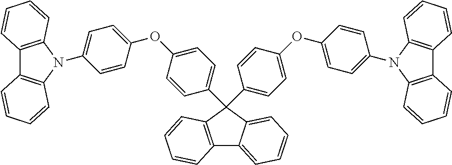 |
JP2007254297 |
 |
JP2007254297 | |
| Indolocabazoles |
 |
WO2007063796 |
 |
WO2007063754 | |
| 5-member ring electron deficient heterocycles (e.g., triazole, oxadiazole) |
 |
J. Appl. Phys. 90, 5048 (2001) |
 |
WO2004107822 | |
| Tetraphenylene complexes |
 |
US20050112407 |
| Metal pheoxypyridine compounds |
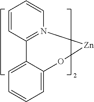 |
WO2005030900 |
| Metal coordination complexes (e.g., Zn, Al with N{circumflex over ( )}N ligands) |
 |
US20040137268, US20040137267 |
| Blue hosts |
| Arylcarbazoles |
 |
Appl. Phys. Lett, 82, 2422 (2003) |
 |
US20070190359 | |
| Dibenzothiophene/ Dibenzofuran- carbazole compounds |
 |
WO2006114966, US20090167162 |
 |
US20090167162 | |
 |
WO2009086028 | |
 |
US20090030202, US20090017330 | |
 |
US20100084966 | |
| Silicon aryl compounds |
 |
US20050238919 |
 |
WO2009003898 | |
| Silicon/Germanium aryl compounds |
 |
EP2034538A |
| Aryl benzoyl ester |
 |
WO2006100298 |
| Carbazole linked by non-conjugated groups |
 |
US20040115476 |
| Aza-carbazoles |
 |
US20060121308 |
| High triplet metal organometallic complex |
 |
U.S. Pat. No. 7,154,114 |
| Phosphoresecnt dopants |
| Red dopants |
| Heavy metal porphyrins (e.g., PtOEP) |
 |
Nature 395, 151 (1998) |
| Iridium(III) organometallic complexes |
 |
Appl. Phys. Lett. 78, 1622 (2001) |
 |
US2006835469 | |
 |
US2006835469 | |
 |
US20060202194 | |
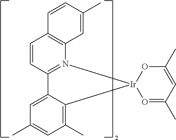 |
US20060202194 | |
 |
US20070087321 | |
 |
US20080261076 US20100090591 | |
 |
US20070087321 | |
 |
Adv. Mater. 19, 739 (2007) | |
 |
WO2009100991 | |
 |
WO2008101842 | |
 |
U.S. Pat. No. 7,232,618 | |
| Platinum(II) organometallic complexes |
 |
WO2003040257 |
 |
US20070103060 | |
| Osminum(III) complexes |
 |
Chem. Mater. 17, 3532 (2005) |
| Ruthenium(II) complexes |
 |
Adv. Mater. 17, 1059 (2005) |
| Rhenium (I), (II) and (III) complexes |
 |
US20050244673 |
| Green dopants |
| Iridium(III) organometallic complexes |
 |
Inorg. Chem. 40, 1704 (2001) |
 |
US20020034656 | |
 |
U.S. Pat. No. 7,332,232 | |
 |
US20090108737 | |
 |
WO2010028151 | |
 |
EP1841834B | |
 |
US20060127696 | |
 |
US20090039776 | |
 |
U.S. Pat. No. 6,921,915 | |
 |
US20100244004 | |
 |
U.S. Pat. No. 6,687,266 | |
 |
Chem. Mater. 16, 2480 (2004) | |
 |
US20070190359 | |
 |
US 20060008670 JP2007123392 | |
 |
WO2010086089, WO2011044988 | |
 |
Adv. Mater. 16, 2003 (2004) | |
 |
Angew. Chem. Int. Ed. 2006, 45, 7800 | |
 |
WO2009050290 | |
 |
US20090165846 | |
 |
US20080015355 | |
 |
US20010015432 | |
 |
US20100295032 | |
| Monomer for polymeric metal organometallic compounds |
 |
U.S. Pat. No. 7,250,226, U.s. Pat. No. 7,396,598 |
| Pt(II) organometallic complexes, including polydentated ligands |
 |
Appl. Phys. Lett. 86, 153505 (2005) |
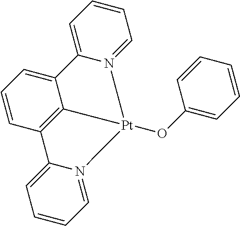 |
Appl. Phys. Lett. 86, 153505 (2005) | |
 |
Chem. Lett. 34, 592 (2005) | |
 |
WO2002015645 | |
 |
US20060263635 | |
 |
US20060182992 US20070103060 | |
| Cu complexes |
 |
WO2009000673 |
 |
US20070111026 | |
| Gold complexes |
 |
Chem. Commun. 2906 (2005) |
| Rhenium(III) complexes |
 |
Inorg. Chem. 42, 1248 (2003) |
| Osmium(II) complexes |
 |
U.S. Pat. No. 7,279,704 |
| Deuterated organometallic complexes |
 |
US20030138657 |
| Organometallic complexes with two or more metal centers |
 |
US20030152802 |
 |
U.S. Pat. No. 7,090,928 | |
| Blue dopants |
| Iridium(III) organometallic complexes |
 |
WO2002002714 |
 |
WO2006009024 | |
 |
US20060251923 US20110057559 US20110204333 | |
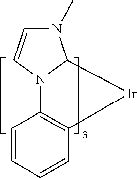 |
U.S. Pat. No. 7,393,599, WO2006056418, US20050260441, WO2005019373 | |
 |
U.S Pat. No. 7,534,505 | |
 |
WO2011051404 | |
 |
U.S. Pat. No. 7,445,855 | |
 |
US20070190359, US20080297033 US20100148663 | |
 |
U.S. Pat. No. 7,338,722 | |
 |
US20020134984 | |
 |
Angew. Chem. Int. Ed. 47, 1 (2008) | |
 |
Chem. Mater. 18, 5119 (2006) | |
 |
Inorg. Chem. 46, 4308 (2007) | |
 |
WO2005123873 | |
 |
WO2005123873 | |
 |
WO2007004380 | |
 |
WO2006082742 | |
| Osmium(II) complexes |
 |
U.S. Pat. No. 7,279,704 |
 |
Organometallics 23, 3745 (2004) | |
| Gold complexes |
|
Appl. Phys. Lett. 74, 1361 (1999) |
| Platinum(II) complexes |
 |
WO2006098120, WO2006103874 |
| Pt tetradentate complexes with at least one metal- carbene bond |
 |
U.S. Pat. No. 7,655,323 |
| Exciton/hole blocking layer materials |
| Bathocuprine compounds (e.g., BCP, BPhen) |
 |
Appl. Phys. Lett. 75, 4 (1999) |
 |
Appl. Phys. Lett. 79, 449 (2001) | |
| Metal 8- hydroxyquinolates (e.g., BAlq) |
 |
Appl. Phys. Lett. 81, 162 (2002) |
| 5-member ring electron deficient heterocycles such as triazole, oxadiazole, imidazole, benzoimidazole |
 |
Appl. Phys. Lett. 81, 162 (2002) |
| Triphenylene compounds |
 |
US20050025993 |
| Fluorinated aromatic compounds |
 |
Appl. Phys. Lett. 79, 156 (2001) |
| Phenothiazine-S- oxide |
 |
WO2008132085 |
| Silylated five- membered nitrogen, oxygen, sulfur or phosphorus dibenzoheterocycles |
 |
WO2010079051 |
| Aza-carbazoles |
 |
US20060121308 |
| Electron transporting materials |
| Anthracene- benzoimidazole compounds |
 |
WO2003060956 |
 |
US20090179554 | |
| Aza triphenylene derivatives |
 |
US20090115316 |
| Anthracene- benzothiazole compounds |
 |
Appl. Phys. Lett. 89, 063504 (2006) |
| Metal 8- hydroxyquinolates (e.g., Alq3, Zrq4) |
 |
Appl. Phys. Lett. 51, 913 (1987) U.S. Pat. No. 7,230,107 |
| Metal hydroxybenoquinolates |
 |
Chem. Lett. 5, 905 (1993) |
| Bathocuprine compounds such as BCP, BPhen, etc |
 |
Appl. Phys. Lett. 91, 263503 (2007) |
 |
Appl. Phys. Lett. 79, 449 (2001) | |
| 5-member ring electron deficient heterocycles (e.g., triazole, oxadiazole, imidazole, benzoimidazole) |
 |
Appl. Phys. Lett. 74, 865 (1999) |
 |
Appl. Phys. Lett. 55, 1489 (1989) | |
 |
Jpn. J. Apply. Phys. 32, L917 (1993) | |
| Silole compounds |
 |
Org. Electron. 4, 113 (2003) |
| Arylborane compounds |
 |
J. Am. Chem. Soc. 120, 9714 (1998) |
| Fluorinated aromatic compounds |
 |
J. Am. Chem. Soc. 122, 1832 (2000) |
| Fullerene (e.g., C60) |
 |
US20090101870 |
| Triazine complexes |
 |
US20040036077 |
| Zn (N{circumflex over ( )}N) complexes |
 |
U.S. Pat. No. 6,528,187 |
Claims (22)
G1-Z, Formula I;


G1-Z, Formula I;


Priority Applications (3)
| Application Number | Priority Date | Filing Date | Title |
|---|---|---|---|
| US13/686,763 US9166175B2 (en) | 2012-11-27 | 2012-11-27 | Organic electroluminescent materials and devices |
| JP2013238020A JP6231859B2 (en) | 2012-11-27 | 2013-11-18 | Organic electroluminescent devices exhibiting delayed fluorescence |
| KR1020130142031A KR102181998B1 (en) | 2012-11-27 | 2013-11-21 | Organic electroluminescent device with delayed fluorescence |
Applications Claiming Priority (1)
| Application Number | Priority Date | Filing Date | Title |
|---|---|---|---|
| US13/686,763 US9166175B2 (en) | 2012-11-27 | 2012-11-27 | Organic electroluminescent materials and devices |
Publications (2)
| Publication Number | Publication Date |
|---|---|
| US20140145151A1 US20140145151A1 (en) | 2014-05-29 |
| US9166175B2 true US9166175B2 (en) | 2015-10-20 |
Family
ID=50772446
Family Applications (1)
| Application Number | Title | Priority Date | Filing Date |
|---|---|---|---|
| US13/686,763 Active 2033-08-15 US9166175B2 (en) | 2012-11-27 | 2012-11-27 | Organic electroluminescent materials and devices |
Country Status (3)
| Country | Link |
|---|---|
| US (1) | US9166175B2 (en) |
| JP (1) | JP6231859B2 (en) |
| KR (1) | KR102181998B1 (en) |
Cited By (2)
| Publication number | Priority date | Publication date | Assignee | Title |
|---|---|---|---|---|
| US10957863B2 (en) | 2017-02-27 | 2021-03-23 | Samsung Electronics Co., Ltd. | Condensed cyclic compound and organic light-emitting device including the same |
| US11393991B2 (en) | 2017-08-01 | 2022-07-19 | Samsung Display Co., Ltd. | Heterocyclic compound and organic electroluminescence device including the same |
Families Citing this family (31)
| Publication number | Priority date | Publication date | Assignee | Title |
|---|---|---|---|---|
| CN107325050A (en) * | 2012-12-28 | 2017-11-07 | 出光兴产株式会社 | Organic electroluminescent element |
| KR20150126381A (en) * | 2013-04-05 | 2015-11-11 | 코니카 미놀타 가부시키가이샤 | Coating liquid for forming light emitting layer, organic electroluminescent element, method for manufacturing organic electroluminescent element, and lighting/display device |
| US10593886B2 (en) | 2013-08-25 | 2020-03-17 | Molecular Glasses, Inc. | OLED devices with improved lifetime using non-crystallizable molecular glass mixture hosts |
| US10461269B2 (en) | 2013-12-20 | 2019-10-29 | Molecular Glasses, Inc. | Crosslinkable, /polymerizable and combinations thereof charge-transporting molecular glass mixtures, luminescent molecular glass mixtures, or combinations thereof for organic light emitting diodes and other organic electronics and photonics applications and method of making same |
| WO2015117100A1 (en) | 2014-02-02 | 2015-08-06 | Molaire Consulting Llc | Noncrystallizable sensitized layers for oled and oeds |
| US10461260B2 (en) * | 2014-06-03 | 2019-10-29 | Universal Display Corporation | Organic electroluminescent materials and devices |
| WO2016010380A1 (en) | 2014-07-17 | 2016-01-21 | Rohm And Haas Electronic Materials Korea Ltd. | Electron transport material and organic electroluminescent device comprising the same |
| KR20160010333A (en) * | 2014-07-17 | 2016-01-27 | 롬엔드하스전자재료코리아유한회사 | Electron transport material and organic electroluminescent device comprising the same |
| KR20160014556A (en) * | 2014-07-29 | 2016-02-11 | 롬엔드하스전자재료코리아유한회사 | Electron Buffering Material and Organic Electroluminescent Device |
| EP3010052B1 (en) * | 2014-10-17 | 2017-08-09 | LG Display Co., Ltd. | Delayed fluorescence compound, and organic light emitting diode and display device using the same |
| KR102503744B1 (en) * | 2014-10-17 | 2023-02-24 | 엘지디스플레이 주식회사 | Delayed fluorescence compound, and Organic light emitting diode device and Display device using the same |
| KR102454043B1 (en) * | 2014-10-17 | 2022-10-14 | 엘지디스플레이 주식회사 | Delayed Fluorescence compound, and Organic light emitting diode device and Display device using the same |
| KR102454042B1 (en) * | 2014-10-17 | 2022-10-14 | 엘지디스플레이 주식회사 | Delayed Fluorescence compound, and Organic light emitting diode device and Display device using the same |
| KR102454044B1 (en) * | 2014-10-17 | 2022-10-14 | 엘지디스플레이 주식회사 | Delayed Fluorescence compound and Organic light emitting diode device and Display device using the same |
| KR102593644B1 (en) * | 2014-11-11 | 2023-10-26 | 롬엔드하스전자재료코리아유한회사 | A plurality of host materials and an organic electroluminescent device comprising the same |
| EP3038181A1 (en) | 2014-12-22 | 2016-06-29 | Solvay SA | Organic electronic devices comprising acridine derivatives in an emissive layer free of heavy atom compounds |
| KR101555680B1 (en) * | 2015-03-03 | 2015-09-25 | 덕산네오룩스 주식회사 | Compound for organic electric element, organic electric element comprising the same and electronic device thereof |
| KR101900370B1 (en) | 2015-05-13 | 2018-09-19 | 삼성에스디아이 주식회사 | Compound for ORGANIC OPTOELECTRIC DEVICE, ORGANIC OPTOELECTRIC DEVICE AND DISPLAY DEVICE |
| CN106699753A (en) * | 2015-07-14 | 2017-05-24 | 上海和辉光电有限公司 | Compound and application thereof |
| WO2017099160A1 (en) * | 2015-12-08 | 2017-06-15 | 出光興産株式会社 | Organic el light emitting apparatus and electronic instrument |
| KR102042191B1 (en) | 2016-03-23 | 2019-11-07 | 삼성에스디아이 주식회사 | Organic compound and organic optoelectric device and display device |
| KR101959047B1 (en) * | 2016-07-15 | 2019-03-18 | 주식회사 엘지화학 | Novel hetero-cyclic compound and organic light emitting device comprising the same |
| WO2018034340A1 (en) * | 2016-08-19 | 2018-02-22 | 株式会社Kyulux | Charge transport material, compound, delayed fluorescent material and organic light emitting element |
| KR20180066339A (en) | 2016-12-07 | 2018-06-19 | 삼성디스플레이 주식회사 | Condensed compound and organic light emitting device comprising the same |
| US10944060B2 (en) * | 2017-05-11 | 2021-03-09 | Universal Display Corporation | Organic electroluminescent materials and devices |
| JP6990996B2 (en) * | 2017-06-01 | 2022-02-03 | 日本放送協会 | Organic electroluminescence elements, display devices, lighting devices |
| US11515477B2 (en) * | 2017-09-06 | 2022-11-29 | Sumitomo Chemical Company, Limited | Light emitting device having thermally activated delayed fluorescent (TADF) compound |
| KR20200011060A (en) | 2018-07-23 | 2020-02-03 | 삼성디스플레이 주식회사 | Organic light-emitting device |
| KR20200100879A (en) | 2019-02-15 | 2020-08-27 | 삼성디스플레이 주식회사 | Organic light emitting device and electronic apparatus comprising the same |
| KR20210059153A (en) | 2019-11-14 | 2021-05-25 | 삼성디스플레이 주식회사 | Organic light emitting device and apparatus comprising the same |
| CN113471376B (en) * | 2021-06-28 | 2024-03-19 | 广东聚华印刷显示技术有限公司 | Light emitting structure, organic light emitting diode and electronic device |
Citations (123)
| Publication number | Priority date | Publication date | Assignee | Title |
|---|---|---|---|---|
| US4769292A (en) | 1987-03-02 | 1988-09-06 | Eastman Kodak Company | Electroluminescent device with modified thin film luminescent zone |
| US5061569A (en) | 1990-07-26 | 1991-10-29 | Eastman Kodak Company | Electroluminescent device with organic electroluminescent medium |
| US5247190A (en) | 1989-04-20 | 1993-09-21 | Cambridge Research And Innovation Limited | Electroluminescent devices |
| EP0650955A1 (en) | 1993-11-01 | 1995-05-03 | Hodogaya Chemical Co., Ltd. | Amine compound and electro-luminescence device comprising same |
| US5703436A (en) | 1994-12-13 | 1997-12-30 | The Trustees Of Princeton University | Transparent contacts for organic devices |
| US5707745A (en) | 1994-12-13 | 1998-01-13 | The Trustees Of Princeton University | Multicolor organic light emitting devices |
| US5834893A (en) | 1996-12-23 | 1998-11-10 | The Trustees Of Princeton University | High efficiency organic light emitting devices with light directing structures |
| US5844363A (en) | 1997-01-23 | 1998-12-01 | The Trustees Of Princeton Univ. | Vacuum deposited, non-polymeric flexible organic light emitting devices |
| US6013982A (en) | 1996-12-23 | 2000-01-11 | The Trustees Of Princeton University | Multicolor display devices |
| US6087196A (en) | 1998-01-30 | 2000-07-11 | The Trustees Of Princeton University | Fabrication of organic semiconductor devices using ink jet printing |
| US6091195A (en) | 1997-02-03 | 2000-07-18 | The Trustees Of Princeton University | Displays having mesa pixel configuration |
| US6097147A (en) | 1998-09-14 | 2000-08-01 | The Trustees Of Princeton University | Structure for high efficiency electroluminescent device |
| WO2001039234A2 (en) | 1999-11-24 | 2001-05-31 | The Trustees Of Princeton University | Organic light emitting diode having a blue phosphorescent molecule as an emitter |
| US6294398B1 (en) | 1999-11-23 | 2001-09-25 | The Trustees Of Princeton University | Method for patterning devices |
| US6303238B1 (en) | 1997-12-01 | 2001-10-16 | The Trustees Of Princeton University | OLEDs doped with phosphorescent compounds |
| US6337102B1 (en) | 1997-11-17 | 2002-01-08 | The Trustees Of Princeton University | Low pressure vapor phase deposition of organic thin films |
| WO2002002714A2 (en) | 2000-06-30 | 2002-01-10 | E.I. Du Pont De Nemours And Company | Electroluminescent iridium compounds with fluorinated phenylpyridines, phenylpyrimidines, and phenylquinolines and devices made with such compounds |
| WO2002015645A1 (en) | 2000-08-11 | 2002-02-21 | The Trustees Of Princeton University | Organometallic compounds and emission-shifting organic electrophosphorescence |
| US20020034656A1 (en) | 1998-09-14 | 2002-03-21 | Thompson Mark E. | Organometallic complexes as phosphorescent emitters in organic LEDs |
| US20020134984A1 (en) | 2001-02-01 | 2002-09-26 | Fuji Photo Film Co., Ltd. | Transition metal complex and light-emitting device |
| US20020158242A1 (en) | 1999-12-31 | 2002-10-31 | Se-Hwan Son | Electronic device comprising organic compound having p-type semiconducting characteristics |
| US6528187B1 (en) | 1998-09-08 | 2003-03-04 | Fuji Photo Film Co., Ltd. | Material for luminescence element and luminescence element using the same |
| WO2003040257A1 (en) | 2001-11-07 | 2003-05-15 | E. I. Du Pont De Nemours And Company | Electroluminescent platinum compounds and devices made with such compounds |
| US20030138657A1 (en) | 2000-12-07 | 2003-07-24 | Canon Kabushiki Kaisha | Deuterated semi-conducting organic compounds used for opto-electronic devices |
| WO2003060956A2 (en) | 2002-01-18 | 2003-07-24 | Lg Chem, Ltd. | New material for transporting electrons and organic electroluminescent display using the same |
| US20030151042A1 (en) | 2002-02-08 | 2003-08-14 | Hueschen Mark R. | Polarization field enhanced tunnel structures |
| US20030152802A1 (en) | 2001-06-19 | 2003-08-14 | Akira Tsuboyama | Metal coordination compound and organic liminescence device |
| US20030175553A1 (en) | 2001-12-28 | 2003-09-18 | Thompson Mark E. | White light emitting oleds from combined monomer and aggregate emission |
| US20030230980A1 (en) | 2002-06-18 | 2003-12-18 | Forrest Stephen R | Very low voltage, high efficiency phosphorescent oled in a p-i-n structure |
| US6687266B1 (en) | 2002-11-08 | 2004-02-03 | Universal Display Corporation | Organic light emitting materials and devices |
| US20040036077A1 (en) | 2002-08-22 | 2004-02-26 | Fuji Photo Film Co., Ltd. | Light emitting element |
| US20040137268A1 (en) | 2002-12-27 | 2004-07-15 | Fuji Photo Film Co., Ltd. | Organic electroluminescent device |
| US20040137267A1 (en) | 2002-12-27 | 2004-07-15 | Fuji Photo Film Co., Ltd. | Organic electroluminescent device |
| US20040174116A1 (en) | 2001-08-20 | 2004-09-09 | Lu Min-Hao Michael | Transparent electrodes |
| WO2004093207A2 (en) | 2003-04-15 | 2004-10-28 | Covion Organic Semiconductors Gmbh | Mixtures of matrix materials and organic semiconductors capable of emission, use of the same and electronic components containing said mixtures |
| WO2004107822A1 (en) | 2003-05-29 | 2004-12-09 | Nippon Steel Chemical Co., Ltd. | Organic electroluminescent element |
| US6835469B2 (en) | 2001-10-17 | 2004-12-28 | The University Of Southern California | Phosphorescent compounds and devices comprising the same |
| JP2005011610A (en) | 2003-06-18 | 2005-01-13 | Nippon Steel Chem Co Ltd | Organic electroluminescent element |
| US20050025993A1 (en) | 2003-07-25 | 2005-02-03 | Thompson Mark E. | Materials and structures for enhancing the performance of organic light emitting devices |
| WO2005014551A1 (en) | 2003-08-07 | 2005-02-17 | Nippon Steel Chemical Co., Ltd. | Aluminum chelate compelx for organic el material |
| WO2005019373A2 (en) | 2003-08-19 | 2005-03-03 | Basf Aktiengesellschaft | Transition metal complexes comprising carbene ligands serving as emitters for organic light-emitting diodes (oled's) |
| WO2005030900A1 (en) | 2003-09-25 | 2005-04-07 | Nippon Steel Chemical Co., Ltd. | Organic electroluminescent device |
| US20050112407A1 (en) | 2003-11-21 | 2005-05-26 | Fuji Photo Film Co., Ltd. | Organic electroluminescent device |
| US6921915B2 (en) | 2001-03-08 | 2005-07-26 | Canon Kabushiki Kaisha | Metal coordination compound, luminescence device and display apparatus |
| WO2005089025A1 (en) | 2004-03-15 | 2005-09-22 | Nippon Steel Chemical Co., Ltd. | Organic electroluminescent device |
| US20050238919A1 (en) | 2004-04-23 | 2005-10-27 | Fuji Photo Film Co., Ltd. | Organic electroluminescent device |
| US20050244673A1 (en) | 2002-08-27 | 2005-11-03 | Fujitsu Limited | Organometallic complex, organic EL element and organic EL display |
| US20050260449A1 (en) | 2004-05-18 | 2005-11-24 | Robert Walters | Complexes with tridentate ligands |
| US20050260441A1 (en) | 2004-05-18 | 2005-11-24 | Thompson Mark E | Luminescent compounds with carbene ligands |
| WO2005123873A1 (en) | 2004-06-17 | 2005-12-29 | Konica Minolta Holdings, Inc. | Organic electroluminescent device material, organic electroluminescent device, display and illuminating device |
| US20060008670A1 (en) | 2004-07-06 | 2006-01-12 | Chun Lin | Organic light emitting materials and devices |
| WO2006009024A1 (en) | 2004-07-23 | 2006-01-26 | Konica Minolta Holdings, Inc. | Organic electroluminescent device, display and illuminating device |
| WO2006056418A2 (en) | 2004-11-25 | 2006-06-01 | Basf Aktiengesellschaft | Use of transition metal carbene complexes in organic light-emitting diodes (oleds) |
| US20060138947A1 (en) * | 2004-12-29 | 2006-06-29 | Macpherson Charles D | Display device |
| WO2006072002A2 (en) | 2004-12-30 | 2006-07-06 | E.I. Dupont De Nemours And Company | Organometallic complexes |
| US7087321B2 (en) | 2003-04-22 | 2006-08-08 | Universal Display Corporation | Organic light emitting devices having reduced pixel shrinkage |
| WO2006082742A1 (en) | 2005-02-04 | 2006-08-10 | Konica Minolta Holdings, Inc. | Organic electroluminescent device material, organic electroluminescent device, display and illuminating device |
| US7090928B2 (en) | 2003-04-01 | 2006-08-15 | The University Of Southern California | Binuclear compounds |
| US20060202194A1 (en) | 2005-03-08 | 2006-09-14 | Jeong Hyun C | Red phosphorescene compounds and organic electroluminescence device using the same |
| WO2006098120A1 (en) | 2005-03-16 | 2006-09-21 | Konica Minolta Holdings, Inc. | Organic electroluminescent device material and organic electroluminescent device |
| WO2006100298A1 (en) | 2005-03-24 | 2006-09-28 | Basf Aktiengesellschaft | Use of compounds containing aromatic or heteroaromatic rings linked via carbonyl group-containing groups, for use as matrix materials in organic light-emitting diodes |
| WO2006103874A1 (en) | 2005-03-29 | 2006-10-05 | Konica Minolta Holdings, Inc. | Organic electroluminescent device material, organic electroluminescent device, display and illuminating device |
| US20060240279A1 (en) | 2005-04-21 | 2006-10-26 | Vadim Adamovich | Non-blocked phosphorescent OLEDs |
| WO2006114966A1 (en) | 2005-04-18 | 2006-11-02 | Konica Minolta Holdings, Inc. | Organic electroluminescent device, display and illuminating device |
| US20060251923A1 (en) | 2005-05-06 | 2006-11-09 | Chun Lin | Stability OLED materials and devices |
| EP1725079A1 (en) | 2004-03-11 | 2006-11-22 | Mitsubishi Chemical Corporation | Composition for charge-transporting film and ion compound, charge-transporting film and organic electroluminescent device using same, and method for manufacturing organic electroluminescent device and method for producing charge-transporting film |
| US20060263635A1 (en) | 2005-05-06 | 2006-11-23 | Fuji Photo Film Co., Ltd. | Organic electroluminescent device |
| WO2006132173A1 (en) | 2005-06-07 | 2006-12-14 | Nippon Steel Chemical Co., Ltd. | Organic metal complex and organic electroluminescent device using same |
| US20060280965A1 (en) | 2005-05-31 | 2006-12-14 | Raymond Kwong | Triphenylene hosts in phosphorescent light emitting diodes |
| US7154114B2 (en) | 2004-05-18 | 2006-12-26 | Universal Display Corporation | Cyclometallated iridium carbene complexes for use as hosts |
| WO2007002683A2 (en) | 2005-06-27 | 2007-01-04 | E. I. Du Pont De Nemours And Company | Electrically conductive polymer compositions |
| US20070007882A1 (en) * | 2003-07-02 | 2007-01-11 | Idemitsu Kosan Co., Ltd. | Organic electroluminescent device and display using same |
| WO2007004380A1 (en) | 2005-07-01 | 2007-01-11 | Konica Minolta Holdings, Inc. | Organic electroluminescent element material, organic electroluminescent element, display device, and lighting equipment |
| JP2007123392A (en) | 2005-10-26 | 2007-05-17 | Konica Minolta Holdings Inc | Organic electroluminescence device, display device and lighting device |
| WO2007063796A1 (en) | 2005-12-01 | 2007-06-07 | Nippon Steel Chemical Co., Ltd. | Organic electroluminescent device |
| WO2007063754A1 (en) | 2005-12-01 | 2007-06-07 | Nippon Steel Chemical Co., Ltd. | Compound for organic electroluminescent element and organic electroluminescent element |
| US7250226B2 (en) | 2001-08-31 | 2007-07-31 | Nippon Hoso Kyokai | Phosphorescent compound, a phosphorescent composition and an organic light-emitting device |
| US20070190359A1 (en) | 2006-02-10 | 2007-08-16 | Knowles David B | Metal complexes of cyclometallated imidazo[1,2-ƒ]phenanthridine and diimidazo[1,2-a:1',2'-c]quinazoline ligands and isoelectronic and benzannulated analogs thereof |
| JP2007254297A (en) | 2006-03-20 | 2007-10-04 | Nippon Steel Chem Co Ltd | Compound of light-emitting layer and organic electroluminescent device |
| US20070278938A1 (en) | 2006-04-26 | 2007-12-06 | Idemitsu Kosan Co., Ltd. | Aromatic amine derivative and electroluminescence device using the same |
| US20080015355A1 (en) | 2004-06-28 | 2008-01-17 | Thomas Schafer | Electroluminescent Metal Complexes With Triazoles And Benzotriazoles |
| US7332232B2 (en) | 2004-02-03 | 2008-02-19 | Universal Display Corporation | OLEDs utilizing multidentate ligand systems |
| US7338722B2 (en) | 2003-03-24 | 2008-03-04 | The University Of Southern California | Phenyl and fluorenyl substituted phenyl-pyrazole complexes of Ir |
| JP2008074939A (en) | 2006-09-21 | 2008-04-03 | Konica Minolta Holdings Inc | Organic electroluminescence element material, organic electroluminescence element, display device and illumination device |
| US20080106190A1 (en) | 2006-08-23 | 2008-05-08 | Idemitsu Kosan Co., Ltd. | Aromatic amine derivatives and organic electroluminescent device using same |
| WO2008056746A1 (en) | 2006-11-09 | 2008-05-15 | Nippon Steel Chemical Co., Ltd. | Compound for organic electroluminescent device and organic electroluminescent device |
| US20080124572A1 (en) | 2006-11-24 | 2008-05-29 | Idemitsu Kosan Co., Ltd. | Aromatic amine derivative and organic electroluminescence device using the same |
| US7393599B2 (en) | 2004-05-18 | 2008-07-01 | The University Of Southern California | Luminescent compounds with carbene ligands |
| US7396598B2 (en) | 2001-06-20 | 2008-07-08 | Showa Denko K.K. | Light emitting material and organic light-emitting device |
| WO2008101842A1 (en) | 2007-02-23 | 2008-08-28 | Basf Se | Electroluminescent metal complexes with benzotriazoles |
| US20080220265A1 (en) | 2006-12-08 | 2008-09-11 | Universal Display Corporation | Cross-linkable Iridium Complexes and Organic Light-Emitting Devices Using the Same |
| US7431968B1 (en) | 2001-09-04 | 2008-10-07 | The Trustees Of Princeton University | Process and apparatus for organic vapor jet deposition |
| US7445855B2 (en) | 2004-05-18 | 2008-11-04 | The University Of Southern California | Cationic metal-carbene complexes |
| WO2008132085A1 (en) | 2007-04-26 | 2008-11-06 | Basf Se | Silanes containing phenothiazine-s-oxide or phenothiazine-s,s-dioxide groups and the use thereof in oleds |
| US20080297033A1 (en) | 2006-02-10 | 2008-12-04 | Knowles David B | Blue phosphorescent imidazophenanthridine materials |
| WO2009000673A2 (en) | 2007-06-22 | 2008-12-31 | Basf Se | Light emitting cu(i) complexes |
| US20090008605A1 (en) | 2007-07-07 | 2009-01-08 | Idemitsu Kosan Co., Ltd. | Naphthalene derivative, material for organic electroluminescence device, and organic electroluminescence device using the same |
| WO2009003898A1 (en) | 2007-07-05 | 2009-01-08 | Basf Se | Organic light-emitting diodes containing carbene transition metal complex emitters and at least one compound selected from disilylcarbazoles, disilyldibenzofurans, disilyldibenzothiophenes, disilyldibenzophospholes, disilyldibenzothiophene s-oxides and disilyldibenzothiophene s,s-dioxides |
| US20090009065A1 (en) | 2007-07-07 | 2009-01-08 | Idemitsu Kosan Co., Ltd. | Organic electroluminescence device and material for organic electroluminescence device |
| US20090017330A1 (en) | 2007-07-10 | 2009-01-15 | Idemitsu Kosan Co., Ltd. | Material for organic electroluminescence device and organic electroluminescence device utilizing the same |
| WO2009008311A1 (en) | 2007-07-07 | 2009-01-15 | Idemitsu Kosan Co., Ltd. | Chrysene derivative and organic electroluminescent device using the same |
| US20090030202A1 (en) | 2007-07-10 | 2009-01-29 | Idemitsu Kosan Co., Ltd. | Material for organic electroluminescent element and organic electroluminescent element employing the same |
| WO2009018009A1 (en) | 2007-07-27 | 2009-02-05 | E. I. Du Pont De Nemours And Company | Aqueous dispersions of electrically conducting polymers containing inorganic nanoparticles |
| US20090039776A1 (en) | 2007-08-09 | 2009-02-12 | Canon Kabushiki Kaisha | Organometallic complex and organic light-emitting element using same |
| WO2009021126A2 (en) | 2007-08-08 | 2009-02-12 | Universal Display Corporation | Benzo-fused thiophene or benzo-fused furan compounds comprising a triphenylene group |
| US20090045731A1 (en) | 2007-07-07 | 2009-02-19 | Idemitsu Kosan Co., Ltd. | Organic electroluminescence device and material for organic electroluminescence device |
| US20090045730A1 (en) | 2007-07-07 | 2009-02-19 | Idemitsu Kosan Co., Ltd. | Organic electroluminescence device and material for organic electroluminescence device |
| EP2034538A1 (en) | 2006-06-02 | 2009-03-11 | Idemitsu Kosan Co., Ltd. | Material for organic electroluminescence element, and organic electroluminescence element using the material |
| WO2009050290A1 (en) | 2007-10-17 | 2009-04-23 | Basf Se | Transition metal complexes having bridged carbene ligands and the use thereof in oleds |
| US20090101870A1 (en) | 2007-10-22 | 2009-04-23 | E. I. Du Pont De Nemours And Company | Electron transport bi-layers and devices made with such bi-layers |
| US20090108737A1 (en) | 2006-12-08 | 2009-04-30 | Raymond Kwong | Light-emitting organometallic complexes |
| US20090115316A1 (en) | 2007-11-02 | 2009-05-07 | Shiying Zheng | Organic electroluminescent device having an azatriphenylene derivative |
| US7534505B2 (en) | 2004-05-18 | 2009-05-19 | The University Of Southern California | Organometallic compounds for use in electroluminescent devices |
| WO2009063833A1 (en) | 2007-11-15 | 2009-05-22 | Idemitsu Kosan Co., Ltd. | Benzochrysene derivative and organic electroluminescent device using the same |
| WO2009062578A1 (en) | 2007-11-12 | 2009-05-22 | Merck Patent Gmbh | Organic electroluminescent devices comprising azomethine-metal complexes |
| WO2009066779A1 (en) | 2007-11-22 | 2009-05-28 | Idemitsu Kosan Co., Ltd. | Organic el element |
| WO2009066778A1 (en) | 2007-11-22 | 2009-05-28 | Idemitsu Kosan Co., Ltd. | Organic el element and solution containing organic el material |
| US20090165846A1 (en) | 2005-09-07 | 2009-07-02 | Universitaet Braunschweig | Triplet emitter having condensed five-membered rings |
| US20090167162A1 (en) | 2007-12-28 | 2009-07-02 | Universal Display Corporation | Dibenzothiophene-containing materials in phosphorescent light emitting diodes |
| WO2009086028A2 (en) | 2007-12-28 | 2009-07-09 | Universal Display Corporation | Carbazole-containing materials in phosphorescent light emitting diodes |
| US20090179554A1 (en) | 2006-05-11 | 2009-07-16 | Hitoshi Kuma | Organic electroluminescent device |
| WO2009100991A1 (en) | 2008-02-12 | 2009-08-20 | Basf Se | Electroluminescent metal complexes with dibenzo[f,h]quinoxalines |
| WO2010107244A2 (en) * | 2009-03-20 | 2010-09-23 | Dow Advanced Display Materials, Ltd. | Novel organic electroluminescent compounds and organic electroluminescent device using the same |
Family Cites Families (3)
| Publication number | Priority date | Publication date | Assignee | Title |
|---|---|---|---|---|
| US8889271B2 (en) * | 2006-11-26 | 2014-11-18 | Duksan High Metal Co., Ltd. | Compound containing a 5-membered heterocycle and organic light-emitting diode using same, and terminal for same |
| KR101477613B1 (en) * | 2009-03-31 | 2014-12-30 | 롬엔드하스전자재료코리아유한회사 | Novel Compounds for Organic Electronic Material and Organic Electronic Device Using the Same |
| US8993129B2 (en) * | 2009-12-07 | 2015-03-31 | Nippon Steel & Sumikin Chemical Co., Ltd. | Fluorescence and delayed fluorescence-type organic light-emitting material and element |
-
2012
- 2012-11-27 US US13/686,763 patent/US9166175B2/en active Active
-
2013
- 2013-11-18 JP JP2013238020A patent/JP6231859B2/en active Active
- 2013-11-21 KR KR1020130142031A patent/KR102181998B1/en active IP Right Grant
Patent Citations (126)
| Publication number | Priority date | Publication date | Assignee | Title |
|---|---|---|---|---|
| US4769292A (en) | 1987-03-02 | 1988-09-06 | Eastman Kodak Company | Electroluminescent device with modified thin film luminescent zone |
| US5247190A (en) | 1989-04-20 | 1993-09-21 | Cambridge Research And Innovation Limited | Electroluminescent devices |
| US5061569A (en) | 1990-07-26 | 1991-10-29 | Eastman Kodak Company | Electroluminescent device with organic electroluminescent medium |
| EP0650955A1 (en) | 1993-11-01 | 1995-05-03 | Hodogaya Chemical Co., Ltd. | Amine compound and electro-luminescence device comprising same |
| US5703436A (en) | 1994-12-13 | 1997-12-30 | The Trustees Of Princeton University | Transparent contacts for organic devices |
| US5707745A (en) | 1994-12-13 | 1998-01-13 | The Trustees Of Princeton University | Multicolor organic light emitting devices |
| US5834893A (en) | 1996-12-23 | 1998-11-10 | The Trustees Of Princeton University | High efficiency organic light emitting devices with light directing structures |
| US6013982A (en) | 1996-12-23 | 2000-01-11 | The Trustees Of Princeton University | Multicolor display devices |
| US5844363A (en) | 1997-01-23 | 1998-12-01 | The Trustees Of Princeton Univ. | Vacuum deposited, non-polymeric flexible organic light emitting devices |
| US6091195A (en) | 1997-02-03 | 2000-07-18 | The Trustees Of Princeton University | Displays having mesa pixel configuration |
| US6337102B1 (en) | 1997-11-17 | 2002-01-08 | The Trustees Of Princeton University | Low pressure vapor phase deposition of organic thin films |
| US6303238B1 (en) | 1997-12-01 | 2001-10-16 | The Trustees Of Princeton University | OLEDs doped with phosphorescent compounds |
| US6087196A (en) | 1998-01-30 | 2000-07-11 | The Trustees Of Princeton University | Fabrication of organic semiconductor devices using ink jet printing |
| US6528187B1 (en) | 1998-09-08 | 2003-03-04 | Fuji Photo Film Co., Ltd. | Material for luminescence element and luminescence element using the same |
| US6097147A (en) | 1998-09-14 | 2000-08-01 | The Trustees Of Princeton University | Structure for high efficiency electroluminescent device |
| US20020034656A1 (en) | 1998-09-14 | 2002-03-21 | Thompson Mark E. | Organometallic complexes as phosphorescent emitters in organic LEDs |
| US6468819B1 (en) | 1999-11-23 | 2002-10-22 | The Trustees Of Princeton University | Method for patterning organic thin film devices using a die |
| US6294398B1 (en) | 1999-11-23 | 2001-09-25 | The Trustees Of Princeton University | Method for patterning devices |
| WO2001039234A2 (en) | 1999-11-24 | 2001-05-31 | The Trustees Of Princeton University | Organic light emitting diode having a blue phosphorescent molecule as an emitter |
| US20020158242A1 (en) | 1999-12-31 | 2002-10-31 | Se-Hwan Son | Electronic device comprising organic compound having p-type semiconducting characteristics |
| WO2002002714A2 (en) | 2000-06-30 | 2002-01-10 | E.I. Du Pont De Nemours And Company | Electroluminescent iridium compounds with fluorinated phenylpyridines, phenylpyrimidines, and phenylquinolines and devices made with such compounds |
| WO2002015645A1 (en) | 2000-08-11 | 2002-02-21 | The Trustees Of Princeton University | Organometallic compounds and emission-shifting organic electrophosphorescence |
| US20030138657A1 (en) | 2000-12-07 | 2003-07-24 | Canon Kabushiki Kaisha | Deuterated semi-conducting organic compounds used for opto-electronic devices |
| US20020134984A1 (en) | 2001-02-01 | 2002-09-26 | Fuji Photo Film Co., Ltd. | Transition metal complex and light-emitting device |
| US6921915B2 (en) | 2001-03-08 | 2005-07-26 | Canon Kabushiki Kaisha | Metal coordination compound, luminescence device and display apparatus |
| US20030152802A1 (en) | 2001-06-19 | 2003-08-14 | Akira Tsuboyama | Metal coordination compound and organic liminescence device |
| US7396598B2 (en) | 2001-06-20 | 2008-07-08 | Showa Denko K.K. | Light emitting material and organic light-emitting device |
| US20040174116A1 (en) | 2001-08-20 | 2004-09-09 | Lu Min-Hao Michael | Transparent electrodes |
| US7250226B2 (en) | 2001-08-31 | 2007-07-31 | Nippon Hoso Kyokai | Phosphorescent compound, a phosphorescent composition and an organic light-emitting device |
| US7431968B1 (en) | 2001-09-04 | 2008-10-07 | The Trustees Of Princeton University | Process and apparatus for organic vapor jet deposition |
| US6835469B2 (en) | 2001-10-17 | 2004-12-28 | The University Of Southern California | Phosphorescent compounds and devices comprising the same |
| WO2003040257A1 (en) | 2001-11-07 | 2003-05-15 | E. I. Du Pont De Nemours And Company | Electroluminescent platinum compounds and devices made with such compounds |
| US20030175553A1 (en) | 2001-12-28 | 2003-09-18 | Thompson Mark E. | White light emitting oleds from combined monomer and aggregate emission |
| WO2003060956A2 (en) | 2002-01-18 | 2003-07-24 | Lg Chem, Ltd. | New material for transporting electrons and organic electroluminescent display using the same |
| US20030151042A1 (en) | 2002-02-08 | 2003-08-14 | Hueschen Mark R. | Polarization field enhanced tunnel structures |
| US20030230980A1 (en) | 2002-06-18 | 2003-12-18 | Forrest Stephen R | Very low voltage, high efficiency phosphorescent oled in a p-i-n structure |
| US20040036077A1 (en) | 2002-08-22 | 2004-02-26 | Fuji Photo Film Co., Ltd. | Light emitting element |
| US20050244673A1 (en) | 2002-08-27 | 2005-11-03 | Fujitsu Limited | Organometallic complex, organic EL element and organic EL display |
| US6687266B1 (en) | 2002-11-08 | 2004-02-03 | Universal Display Corporation | Organic light emitting materials and devices |
| US20040137267A1 (en) | 2002-12-27 | 2004-07-15 | Fuji Photo Film Co., Ltd. | Organic electroluminescent device |
| US20040137268A1 (en) | 2002-12-27 | 2004-07-15 | Fuji Photo Film Co., Ltd. | Organic electroluminescent device |
| US7338722B2 (en) | 2003-03-24 | 2008-03-04 | The University Of Southern California | Phenyl and fluorenyl substituted phenyl-pyrazole complexes of Ir |
| US7090928B2 (en) | 2003-04-01 | 2006-08-15 | The University Of Southern California | Binuclear compounds |
| WO2004093207A2 (en) | 2003-04-15 | 2004-10-28 | Covion Organic Semiconductors Gmbh | Mixtures of matrix materials and organic semiconductors capable of emission, use of the same and electronic components containing said mixtures |
| US7087321B2 (en) | 2003-04-22 | 2006-08-08 | Universal Display Corporation | Organic light emitting devices having reduced pixel shrinkage |
| WO2004107822A1 (en) | 2003-05-29 | 2004-12-09 | Nippon Steel Chemical Co., Ltd. | Organic electroluminescent element |
| JP2005011610A (en) | 2003-06-18 | 2005-01-13 | Nippon Steel Chem Co Ltd | Organic electroluminescent element |
| US20070007882A1 (en) * | 2003-07-02 | 2007-01-11 | Idemitsu Kosan Co., Ltd. | Organic electroluminescent device and display using same |
| US20050025993A1 (en) | 2003-07-25 | 2005-02-03 | Thompson Mark E. | Materials and structures for enhancing the performance of organic light emitting devices |
| WO2005014551A1 (en) | 2003-08-07 | 2005-02-17 | Nippon Steel Chemical Co., Ltd. | Aluminum chelate compelx for organic el material |
| WO2005019373A2 (en) | 2003-08-19 | 2005-03-03 | Basf Aktiengesellschaft | Transition metal complexes comprising carbene ligands serving as emitters for organic light-emitting diodes (oled's) |
| WO2005030900A1 (en) | 2003-09-25 | 2005-04-07 | Nippon Steel Chemical Co., Ltd. | Organic electroluminescent device |
| US20050112407A1 (en) | 2003-11-21 | 2005-05-26 | Fuji Photo Film Co., Ltd. | Organic electroluminescent device |
| US7332232B2 (en) | 2004-02-03 | 2008-02-19 | Universal Display Corporation | OLEDs utilizing multidentate ligand systems |
| EP1725079A1 (en) | 2004-03-11 | 2006-11-22 | Mitsubishi Chemical Corporation | Composition for charge-transporting film and ion compound, charge-transporting film and organic electroluminescent device using same, and method for manufacturing organic electroluminescent device and method for producing charge-transporting film |
| WO2005089025A1 (en) | 2004-03-15 | 2005-09-22 | Nippon Steel Chemical Co., Ltd. | Organic electroluminescent device |
| US20050238919A1 (en) | 2004-04-23 | 2005-10-27 | Fuji Photo Film Co., Ltd. | Organic electroluminescent device |
| US7279704B2 (en) | 2004-05-18 | 2007-10-09 | The University Of Southern California | Complexes with tridentate ligands |
| US20050260449A1 (en) | 2004-05-18 | 2005-11-24 | Robert Walters | Complexes with tridentate ligands |
| US7154114B2 (en) | 2004-05-18 | 2006-12-26 | Universal Display Corporation | Cyclometallated iridium carbene complexes for use as hosts |
| US7393599B2 (en) | 2004-05-18 | 2008-07-01 | The University Of Southern California | Luminescent compounds with carbene ligands |
| US7534505B2 (en) | 2004-05-18 | 2009-05-19 | The University Of Southern California | Organometallic compounds for use in electroluminescent devices |
| US7445855B2 (en) | 2004-05-18 | 2008-11-04 | The University Of Southern California | Cationic metal-carbene complexes |
| US20050260441A1 (en) | 2004-05-18 | 2005-11-24 | Thompson Mark E | Luminescent compounds with carbene ligands |
| WO2005123873A1 (en) | 2004-06-17 | 2005-12-29 | Konica Minolta Holdings, Inc. | Organic electroluminescent device material, organic electroluminescent device, display and illuminating device |
| US20080015355A1 (en) | 2004-06-28 | 2008-01-17 | Thomas Schafer | Electroluminescent Metal Complexes With Triazoles And Benzotriazoles |
| US20060008670A1 (en) | 2004-07-06 | 2006-01-12 | Chun Lin | Organic light emitting materials and devices |
| WO2006009024A1 (en) | 2004-07-23 | 2006-01-26 | Konica Minolta Holdings, Inc. | Organic electroluminescent device, display and illuminating device |
| US20080018221A1 (en) | 2004-11-25 | 2008-01-24 | Basf Aktiengesellschaft | Use Of Transition Metal Carbene Complexes In Organic Light-Emitting Diodes (Oleds) |
| WO2006056418A2 (en) | 2004-11-25 | 2006-06-01 | Basf Aktiengesellschaft | Use of transition metal carbene complexes in organic light-emitting diodes (oleds) |
| US20060138947A1 (en) * | 2004-12-29 | 2006-06-29 | Macpherson Charles D | Display device |
| WO2006072002A2 (en) | 2004-12-30 | 2006-07-06 | E.I. Dupont De Nemours And Company | Organometallic complexes |
| WO2006082742A1 (en) | 2005-02-04 | 2006-08-10 | Konica Minolta Holdings, Inc. | Organic electroluminescent device material, organic electroluminescent device, display and illuminating device |
| US20060202194A1 (en) | 2005-03-08 | 2006-09-14 | Jeong Hyun C | Red phosphorescene compounds and organic electroluminescence device using the same |
| WO2006098120A1 (en) | 2005-03-16 | 2006-09-21 | Konica Minolta Holdings, Inc. | Organic electroluminescent device material and organic electroluminescent device |
| WO2006100298A1 (en) | 2005-03-24 | 2006-09-28 | Basf Aktiengesellschaft | Use of compounds containing aromatic or heteroaromatic rings linked via carbonyl group-containing groups, for use as matrix materials in organic light-emitting diodes |
| WO2006103874A1 (en) | 2005-03-29 | 2006-10-05 | Konica Minolta Holdings, Inc. | Organic electroluminescent device material, organic electroluminescent device, display and illuminating device |
| WO2006114966A1 (en) | 2005-04-18 | 2006-11-02 | Konica Minolta Holdings, Inc. | Organic electroluminescent device, display and illuminating device |
| US20060240279A1 (en) | 2005-04-21 | 2006-10-26 | Vadim Adamovich | Non-blocked phosphorescent OLEDs |
| US20060251923A1 (en) | 2005-05-06 | 2006-11-09 | Chun Lin | Stability OLED materials and devices |
| US20060263635A1 (en) | 2005-05-06 | 2006-11-23 | Fuji Photo Film Co., Ltd. | Organic electroluminescent device |
| US20060280965A1 (en) | 2005-05-31 | 2006-12-14 | Raymond Kwong | Triphenylene hosts in phosphorescent light emitting diodes |
| WO2006132173A1 (en) | 2005-06-07 | 2006-12-14 | Nippon Steel Chemical Co., Ltd. | Organic metal complex and organic electroluminescent device using same |
| WO2007002683A2 (en) | 2005-06-27 | 2007-01-04 | E. I. Du Pont De Nemours And Company | Electrically conductive polymer compositions |
| WO2007004380A1 (en) | 2005-07-01 | 2007-01-11 | Konica Minolta Holdings, Inc. | Organic electroluminescent element material, organic electroluminescent element, display device, and lighting equipment |
| US20090165846A1 (en) | 2005-09-07 | 2009-07-02 | Universitaet Braunschweig | Triplet emitter having condensed five-membered rings |
| JP2007123392A (en) | 2005-10-26 | 2007-05-17 | Konica Minolta Holdings Inc | Organic electroluminescence device, display device and lighting device |
| WO2007063754A1 (en) | 2005-12-01 | 2007-06-07 | Nippon Steel Chemical Co., Ltd. | Compound for organic electroluminescent element and organic electroluminescent element |
| WO2007063796A1 (en) | 2005-12-01 | 2007-06-07 | Nippon Steel Chemical Co., Ltd. | Organic electroluminescent device |
| US20080297033A1 (en) | 2006-02-10 | 2008-12-04 | Knowles David B | Blue phosphorescent imidazophenanthridine materials |
| US20070190359A1 (en) | 2006-02-10 | 2007-08-16 | Knowles David B | Metal complexes of cyclometallated imidazo[1,2-ƒ]phenanthridine and diimidazo[1,2-a:1',2'-c]quinazoline ligands and isoelectronic and benzannulated analogs thereof |
| JP2007254297A (en) | 2006-03-20 | 2007-10-04 | Nippon Steel Chem Co Ltd | Compound of light-emitting layer and organic electroluminescent device |
| US20070278938A1 (en) | 2006-04-26 | 2007-12-06 | Idemitsu Kosan Co., Ltd. | Aromatic amine derivative and electroluminescence device using the same |
| US20090179554A1 (en) | 2006-05-11 | 2009-07-16 | Hitoshi Kuma | Organic electroluminescent device |
| EP2034538A1 (en) | 2006-06-02 | 2009-03-11 | Idemitsu Kosan Co., Ltd. | Material for organic electroluminescence element, and organic electroluminescence element using the material |
| US20080106190A1 (en) | 2006-08-23 | 2008-05-08 | Idemitsu Kosan Co., Ltd. | Aromatic amine derivatives and organic electroluminescent device using same |
| JP2008074939A (en) | 2006-09-21 | 2008-04-03 | Konica Minolta Holdings Inc | Organic electroluminescence element material, organic electroluminescence element, display device and illumination device |
| WO2008056746A1 (en) | 2006-11-09 | 2008-05-15 | Nippon Steel Chemical Co., Ltd. | Compound for organic electroluminescent device and organic electroluminescent device |
| US20080124572A1 (en) | 2006-11-24 | 2008-05-29 | Idemitsu Kosan Co., Ltd. | Aromatic amine derivative and organic electroluminescence device using the same |
| US20090108737A1 (en) | 2006-12-08 | 2009-04-30 | Raymond Kwong | Light-emitting organometallic complexes |
| US20080220265A1 (en) | 2006-12-08 | 2008-09-11 | Universal Display Corporation | Cross-linkable Iridium Complexes and Organic Light-Emitting Devices Using the Same |
| WO2008101842A1 (en) | 2007-02-23 | 2008-08-28 | Basf Se | Electroluminescent metal complexes with benzotriazoles |
| WO2008132085A1 (en) | 2007-04-26 | 2008-11-06 | Basf Se | Silanes containing phenothiazine-s-oxide or phenothiazine-s,s-dioxide groups and the use thereof in oleds |
| WO2009000673A2 (en) | 2007-06-22 | 2008-12-31 | Basf Se | Light emitting cu(i) complexes |
| WO2009003898A1 (en) | 2007-07-05 | 2009-01-08 | Basf Se | Organic light-emitting diodes containing carbene transition metal complex emitters and at least one compound selected from disilylcarbazoles, disilyldibenzofurans, disilyldibenzothiophenes, disilyldibenzophospholes, disilyldibenzothiophene s-oxides and disilyldibenzothiophene s,s-dioxides |
| US20090045731A1 (en) | 2007-07-07 | 2009-02-19 | Idemitsu Kosan Co., Ltd. | Organic electroluminescence device and material for organic electroluminescence device |
| US20090045730A1 (en) | 2007-07-07 | 2009-02-19 | Idemitsu Kosan Co., Ltd. | Organic electroluminescence device and material for organic electroluminescence device |
| US20090008605A1 (en) | 2007-07-07 | 2009-01-08 | Idemitsu Kosan Co., Ltd. | Naphthalene derivative, material for organic electroluminescence device, and organic electroluminescence device using the same |
| WO2009008311A1 (en) | 2007-07-07 | 2009-01-15 | Idemitsu Kosan Co., Ltd. | Chrysene derivative and organic electroluminescent device using the same |
| US20090009065A1 (en) | 2007-07-07 | 2009-01-08 | Idemitsu Kosan Co., Ltd. | Organic electroluminescence device and material for organic electroluminescence device |
| US20090030202A1 (en) | 2007-07-10 | 2009-01-29 | Idemitsu Kosan Co., Ltd. | Material for organic electroluminescent element and organic electroluminescent element employing the same |
| US20090017330A1 (en) | 2007-07-10 | 2009-01-15 | Idemitsu Kosan Co., Ltd. | Material for organic electroluminescence device and organic electroluminescence device utilizing the same |
| WO2009018009A1 (en) | 2007-07-27 | 2009-02-05 | E. I. Du Pont De Nemours And Company | Aqueous dispersions of electrically conducting polymers containing inorganic nanoparticles |
| WO2009021126A2 (en) | 2007-08-08 | 2009-02-12 | Universal Display Corporation | Benzo-fused thiophene or benzo-fused furan compounds comprising a triphenylene group |
| US20090039776A1 (en) | 2007-08-09 | 2009-02-12 | Canon Kabushiki Kaisha | Organometallic complex and organic light-emitting element using same |
| WO2009050290A1 (en) | 2007-10-17 | 2009-04-23 | Basf Se | Transition metal complexes having bridged carbene ligands and the use thereof in oleds |
| US20090101870A1 (en) | 2007-10-22 | 2009-04-23 | E. I. Du Pont De Nemours And Company | Electron transport bi-layers and devices made with such bi-layers |
| US20090115316A1 (en) | 2007-11-02 | 2009-05-07 | Shiying Zheng | Organic electroluminescent device having an azatriphenylene derivative |
| WO2009062578A1 (en) | 2007-11-12 | 2009-05-22 | Merck Patent Gmbh | Organic electroluminescent devices comprising azomethine-metal complexes |
| WO2009063833A1 (en) | 2007-11-15 | 2009-05-22 | Idemitsu Kosan Co., Ltd. | Benzochrysene derivative and organic electroluminescent device using the same |
| WO2009066779A1 (en) | 2007-11-22 | 2009-05-28 | Idemitsu Kosan Co., Ltd. | Organic el element |
| WO2009066778A1 (en) | 2007-11-22 | 2009-05-28 | Idemitsu Kosan Co., Ltd. | Organic el element and solution containing organic el material |
| US20090167162A1 (en) | 2007-12-28 | 2009-07-02 | Universal Display Corporation | Dibenzothiophene-containing materials in phosphorescent light emitting diodes |
| WO2009086028A2 (en) | 2007-12-28 | 2009-07-09 | Universal Display Corporation | Carbazole-containing materials in phosphorescent light emitting diodes |
| WO2009100991A1 (en) | 2008-02-12 | 2009-08-20 | Basf Se | Electroluminescent metal complexes with dibenzo[f,h]quinoxalines |
| WO2010107244A2 (en) * | 2009-03-20 | 2010-09-23 | Dow Advanced Display Materials, Ltd. | Novel organic electroluminescent compounds and organic electroluminescent device using the same |
Non-Patent Citations (51)
Cited By (2)
| Publication number | Priority date | Publication date | Assignee | Title |
|---|---|---|---|---|
| US10957863B2 (en) | 2017-02-27 | 2021-03-23 | Samsung Electronics Co., Ltd. | Condensed cyclic compound and organic light-emitting device including the same |
| US11393991B2 (en) | 2017-08-01 | 2022-07-19 | Samsung Display Co., Ltd. | Heterocyclic compound and organic electroluminescence device including the same |
Also Published As
| Publication number | Publication date |
|---|---|
| KR20140067914A (en) | 2014-06-05 |
| KR102181998B1 (en) | 2020-11-24 |
| US20140145151A1 (en) | 2014-05-29 |
| JP2014107557A (en) | 2014-06-09 |
| JP6231859B2 (en) | 2017-11-15 |
Similar Documents
| Publication | Publication Date | Title |
|---|---|---|
| US11716902B2 (en) | Organic electroluminescent materials and devices | |
| US11289659B2 (en) | Organic electroluminescent materials and devices | |
| US9166175B2 (en) | Organic electroluminescent materials and devices | |
| US9627631B2 (en) | Organic electroluminescent materials and devices | |
| US20200044163A1 (en) | Organic electroluminescent materials and devices | |
| US20190326528A1 (en) | Organic electroluminescent materials and devices | |
| US11696459B2 (en) | Phosphorescence-sensitized delayed fluorescence light emitting system | |
| US9935276B2 (en) | Organic electroluminescent materials and devices | |
| US20140131665A1 (en) | Organic Electroluminescent Device With Delayed Fluorescence | |
| US9773985B2 (en) | Organic electroluminescent materials and devices | |
| US11600782B2 (en) | Organic electroluminescent materials and devices | |
| US20150115250A1 (en) | Organic electroluminescent materials and devices | |
| US9653691B2 (en) | Phosphorescence-sensitizing fluorescence material system | |
| US9252377B2 (en) | Inorganic hosts in OLEDs | |
| US9287513B2 (en) | Organic electroluminescent materials and devices | |
| US9876173B2 (en) | Organic electroluminescent materials and devices | |
| US9741941B2 (en) | Organic electroluminescent materials and devices | |
| US9761814B2 (en) | Organic light-emitting materials and devices | |
| US20150021557A1 (en) | Organic electroluminescent materials and devices |
Legal Events
| Date | Code | Title | Description |
|---|---|---|---|
| AS | Assignment |
Owner name: UNIVERSAL DISPLAY CORPORATION, NEW JERSEY Free format text: ASSIGNMENT OF ASSIGNORS INTEREST;ASSIGNORS:XIA, CHUANJUN;LIN, CHUN;REEL/FRAME:029451/0712 Effective date: 20121207 |
|
| FEPP | Fee payment procedure |
Free format text: PAYOR NUMBER ASSIGNED (ORIGINAL EVENT CODE: ASPN); ENTITY STATUS OF PATENT OWNER: LARGE ENTITY |
|
| STCF | Information on status: patent grant |
Free format text: PATENTED CASE |
|
| CC | Certificate of correction | ||
| MAFP | Maintenance fee payment |
Free format text: PAYMENT OF MAINTENANCE FEE, 4TH YEAR, LARGE ENTITY (ORIGINAL EVENT CODE: M1551); ENTITY STATUS OF PATENT OWNER: LARGE ENTITY Year of fee payment: 4 |
|
| MAFP | Maintenance fee payment |
Free format text: PAYMENT OF MAINTENANCE FEE, 8TH YEAR, LARGE ENTITY (ORIGINAL EVENT CODE: M1552); ENTITY STATUS OF PATENT OWNER: LARGE ENTITY Year of fee payment: 8 |