US9159924B2 - Method of preparing carbon thin film, electronics comprising carbon thin film, and electrochemical device comprising carbon thin film - Google Patents
Method of preparing carbon thin film, electronics comprising carbon thin film, and electrochemical device comprising carbon thin film Download PDFInfo
- Publication number
- US9159924B2 US9159924B2 US13/187,671 US201113187671A US9159924B2 US 9159924 B2 US9159924 B2 US 9159924B2 US 201113187671 A US201113187671 A US 201113187671A US 9159924 B2 US9159924 B2 US 9159924B2
- Authority
- US
- United States
- Prior art keywords
- group
- substituted
- thin film
- unsubstituted
- carbon thin
- Prior art date
- Legal status (The legal status is an assumption and is not a legal conclusion. Google has not performed a legal analysis and makes no representation as to the accuracy of the status listed.)
- Expired - Fee Related, expires
Links
- OKTJSMMVPCPJKN-UHFFFAOYSA-N Carbon Chemical compound [C] OKTJSMMVPCPJKN-UHFFFAOYSA-N 0.000 title claims abstract description 209
- 239000010409 thin film Substances 0.000 title claims abstract description 176
- 229910052799 carbon Inorganic materials 0.000 title claims abstract description 175
- 238000000034 method Methods 0.000 title claims abstract description 71
- 239000010410 layer Substances 0.000 claims description 177
- 229920000642 polymer Polymers 0.000 claims description 145
- 239000000758 substrate Substances 0.000 claims description 66
- 239000011241 protective layer Substances 0.000 claims description 46
- PXHVJJICTQNCMI-UHFFFAOYSA-N Nickel Chemical compound [Ni] PXHVJJICTQNCMI-UHFFFAOYSA-N 0.000 claims description 42
- 238000010438 heat treatment Methods 0.000 claims description 40
- 239000000463 material Substances 0.000 claims description 37
- VYPSYNLAJGMNEJ-UHFFFAOYSA-N Silicium dioxide Chemical compound O=[Si]=O VYPSYNLAJGMNEJ-UHFFFAOYSA-N 0.000 claims description 24
- 239000003054 catalyst Substances 0.000 claims description 24
- 229910021389 graphene Inorganic materials 0.000 claims description 24
- 125000004093 cyano group Chemical group *C#N 0.000 claims description 22
- 239000000203 mixture Substances 0.000 claims description 22
- 238000000576 coating method Methods 0.000 claims description 21
- 125000003178 carboxy group Chemical group [H]OC(*)=O 0.000 claims description 20
- 229910052751 metal Inorganic materials 0.000 claims description 20
- 239000002184 metal Substances 0.000 claims description 20
- 125000000449 nitro group Chemical group [O-][N+](*)=O 0.000 claims description 20
- 239000011777 magnesium Substances 0.000 claims description 18
- 229910052814 silicon oxide Inorganic materials 0.000 claims description 18
- KDLHZDBZIXYQEI-UHFFFAOYSA-N Palladium Chemical compound [Pd] KDLHZDBZIXYQEI-UHFFFAOYSA-N 0.000 claims description 15
- 239000010949 copper Substances 0.000 claims description 15
- 239000010931 gold Substances 0.000 claims description 15
- 229910052782 aluminium Inorganic materials 0.000 claims description 13
- XAGFODPZIPBFFR-UHFFFAOYSA-N aluminium Chemical compound [Al] XAGFODPZIPBFFR-UHFFFAOYSA-N 0.000 claims description 13
- 125000003118 aryl group Chemical group 0.000 claims description 13
- 125000004435 hydrogen atom Chemical class [H]* 0.000 claims description 13
- 239000002904 solvent Substances 0.000 claims description 13
- 125000001072 heteroaryl group Chemical group 0.000 claims description 12
- 229910044991 metal oxide Inorganic materials 0.000 claims description 12
- 150000004706 metal oxides Chemical class 0.000 claims description 12
- 229910002804 graphite Inorganic materials 0.000 claims description 11
- 239000010439 graphite Substances 0.000 claims description 11
- RYGMFSIKBFXOCR-UHFFFAOYSA-N Copper Chemical compound [Cu] RYGMFSIKBFXOCR-UHFFFAOYSA-N 0.000 claims description 10
- 239000011888 foil Substances 0.000 claims description 10
- 125000005843 halogen group Chemical group 0.000 claims description 10
- 125000002887 hydroxy group Chemical group [H]O* 0.000 claims description 10
- 229910052757 nitrogen Inorganic materials 0.000 claims description 10
- FYYHWMGAXLPEAU-UHFFFAOYSA-N Magnesium Chemical compound [Mg] FYYHWMGAXLPEAU-UHFFFAOYSA-N 0.000 claims description 9
- XUIMIQQOPSSXEZ-UHFFFAOYSA-N Silicon Chemical compound [Si] XUIMIQQOPSSXEZ-UHFFFAOYSA-N 0.000 claims description 9
- 239000005083 Zinc sulfide Substances 0.000 claims description 9
- 229910052749 magnesium Inorganic materials 0.000 claims description 9
- 229910052759 nickel Inorganic materials 0.000 claims description 9
- 238000000059 patterning Methods 0.000 claims description 9
- 229910052710 silicon Inorganic materials 0.000 claims description 9
- 239000010703 silicon Substances 0.000 claims description 9
- 229910052984 zinc sulfide Inorganic materials 0.000 claims description 9
- 229910052802 copper Inorganic materials 0.000 claims description 8
- 239000010948 rhodium Substances 0.000 claims description 8
- 125000000923 (C1-C30) alkyl group Chemical group 0.000 claims description 7
- PCHJSUWPFVWCPO-UHFFFAOYSA-N gold Chemical compound [Au] PCHJSUWPFVWCPO-UHFFFAOYSA-N 0.000 claims description 7
- 229910052737 gold Inorganic materials 0.000 claims description 7
- 229910052750 molybdenum Inorganic materials 0.000 claims description 7
- ZOKXTWBITQBERF-UHFFFAOYSA-N Molybdenum Chemical compound [Mo] ZOKXTWBITQBERF-UHFFFAOYSA-N 0.000 claims description 6
- 239000012298 atmosphere Substances 0.000 claims description 6
- 239000011651 chromium Substances 0.000 claims description 6
- 239000011733 molybdenum Substances 0.000 claims description 6
- 239000010936 titanium Substances 0.000 claims description 6
- 125000000008 (C1-C10) alkyl group Chemical group 0.000 claims description 5
- 230000008018 melting Effects 0.000 claims description 5
- 238000002844 melting Methods 0.000 claims description 5
- 229910052763 palladium Inorganic materials 0.000 claims description 5
- 229910052594 sapphire Inorganic materials 0.000 claims description 5
- 239000010980 sapphire Substances 0.000 claims description 5
- 229910052709 silver Inorganic materials 0.000 claims description 5
- 239000004332 silver Substances 0.000 claims description 5
- 238000005979 thermal decomposition reaction Methods 0.000 claims description 5
- 125000000027 (C1-C10) alkoxy group Chemical group 0.000 claims description 4
- 229910052582 BN Inorganic materials 0.000 claims description 4
- PZNSFCLAULLKQX-UHFFFAOYSA-N Boron nitride Chemical compound N#B PZNSFCLAULLKQX-UHFFFAOYSA-N 0.000 claims description 4
- 125000003545 alkoxy group Chemical group 0.000 claims description 4
- 125000005907 alkyl ester group Chemical group 0.000 claims description 4
- 125000003710 aryl alkyl group Chemical group 0.000 claims description 4
- 150000007860 aryl ester derivatives Chemical group 0.000 claims description 4
- 125000004104 aryloxy group Chemical group 0.000 claims description 4
- 230000027455 binding Effects 0.000 claims description 4
- 238000009739 binding Methods 0.000 claims description 4
- 125000004446 heteroarylalkyl group Chemical group 0.000 claims description 4
- 125000005553 heteroaryloxy group Chemical group 0.000 claims description 4
- 125000000592 heterocycloalkyl group Chemical group 0.000 claims description 4
- 229910052739 hydrogen Inorganic materials 0.000 claims description 4
- 239000001257 hydrogen Substances 0.000 claims description 4
- 229910052760 oxygen Inorganic materials 0.000 claims description 4
- 229920000307 polymer substrate Polymers 0.000 claims description 4
- 239000002243 precursor Substances 0.000 claims description 4
- 229910052703 rhodium Inorganic materials 0.000 claims description 4
- MHOVAHRLVXNVSD-UHFFFAOYSA-N rhodium atom Chemical compound [Rh] MHOVAHRLVXNVSD-UHFFFAOYSA-N 0.000 claims description 4
- 239000002356 single layer Substances 0.000 claims description 4
- DRDVZXDWVBGGMH-UHFFFAOYSA-N zinc;sulfide Chemical compound [S-2].[Zn+2] DRDVZXDWVBGGMH-UHFFFAOYSA-N 0.000 claims description 4
- VYZAMTAEIAYCRO-UHFFFAOYSA-N Chromium Chemical compound [Cr] VYZAMTAEIAYCRO-UHFFFAOYSA-N 0.000 claims description 3
- XEEYBQQBJWHFJM-UHFFFAOYSA-N Iron Chemical compound [Fe] XEEYBQQBJWHFJM-UHFFFAOYSA-N 0.000 claims description 3
- BQCADISMDOOEFD-UHFFFAOYSA-N Silver Chemical compound [Ag] BQCADISMDOOEFD-UHFFFAOYSA-N 0.000 claims description 3
- RTAQQCXQSZGOHL-UHFFFAOYSA-N Titanium Chemical compound [Ti] RTAQQCXQSZGOHL-UHFFFAOYSA-N 0.000 claims description 3
- 229910052770 Uranium Inorganic materials 0.000 claims description 3
- 229910052804 chromium Inorganic materials 0.000 claims description 3
- 229910017052 cobalt Inorganic materials 0.000 claims description 3
- 239000010941 cobalt Substances 0.000 claims description 3
- GUTLYIVDDKVIGB-UHFFFAOYSA-N cobalt atom Chemical compound [Co] GUTLYIVDDKVIGB-UHFFFAOYSA-N 0.000 claims description 3
- 125000001624 naphthyl group Chemical group 0.000 claims description 3
- 125000001997 phenyl group Chemical group [H]C1=C([H])C([H])=C(*)C([H])=C1[H] 0.000 claims description 3
- 125000004076 pyridyl group Chemical group 0.000 claims description 3
- VSZWPYCFIRKVQL-UHFFFAOYSA-N selanylidenegallium;selenium Chemical compound [Se].[Se]=[Ga].[Se]=[Ga] VSZWPYCFIRKVQL-UHFFFAOYSA-N 0.000 claims description 3
- 230000000087 stabilizing effect Effects 0.000 claims description 3
- 239000010935 stainless steel Substances 0.000 claims description 3
- 229910001220 stainless steel Inorganic materials 0.000 claims description 3
- 229910052717 sulfur Inorganic materials 0.000 claims description 3
- 229910052715 tantalum Inorganic materials 0.000 claims description 3
- GUVRBAGPIYLISA-UHFFFAOYSA-N tantalum atom Chemical compound [Ta] GUVRBAGPIYLISA-UHFFFAOYSA-N 0.000 claims description 3
- 229910052719 titanium Inorganic materials 0.000 claims description 3
- WFKWXMTUELFFGS-UHFFFAOYSA-N tungsten Chemical compound [W] WFKWXMTUELFFGS-UHFFFAOYSA-N 0.000 claims description 3
- 229910052721 tungsten Inorganic materials 0.000 claims description 3
- 239000010937 tungsten Substances 0.000 claims description 3
- JFALSRSLKYAFGM-UHFFFAOYSA-N uranium(0) Chemical compound [U] JFALSRSLKYAFGM-UHFFFAOYSA-N 0.000 claims description 3
- LEONUFNNVUYDNQ-UHFFFAOYSA-N vanadium atom Chemical compound [V] LEONUFNNVUYDNQ-UHFFFAOYSA-N 0.000 claims description 3
- -1 SiO2 Chemical compound 0.000 description 32
- 239000004065 semiconductor Substances 0.000 description 22
- 229920002239 polyacrylonitrile Polymers 0.000 description 15
- 238000000151 deposition Methods 0.000 description 14
- 230000008021 deposition Effects 0.000 description 14
- 238000001237 Raman spectrum Methods 0.000 description 11
- 239000011248 coating agent Substances 0.000 description 11
- 0 *C([1*])([2*])C(*)([3*])C#C.*C([4*])([5*])C(*)([6*])/C([7*])=[Y]\[Y].*C([8*])([9*])C(*)([10*])C(=C)[Y][Y][Y][Y].C Chemical compound *C([1*])([2*])C(*)([3*])C#C.*C([4*])([5*])C(*)([6*])/C([7*])=[Y]\[Y].*C([8*])([9*])C(*)([10*])C(=C)[Y][Y][Y][Y].C 0.000 description 10
- 150000001875 compounds Chemical class 0.000 description 10
- 239000000523 sample Substances 0.000 description 10
- 238000004528 spin coating Methods 0.000 description 10
- 239000004793 Polystyrene Substances 0.000 description 9
- 230000000052 comparative effect Effects 0.000 description 9
- 229920003229 poly(methyl methacrylate) Polymers 0.000 description 8
- 239000004926 polymethyl methacrylate Substances 0.000 description 8
- 229920002223 polystyrene Polymers 0.000 description 8
- ZMXDDKWLCZADIW-UHFFFAOYSA-N N,N-Dimethylformamide Chemical compound CN(C)C=O ZMXDDKWLCZADIW-UHFFFAOYSA-N 0.000 description 7
- 238000013086 organic photovoltaic Methods 0.000 description 7
- 238000001771 vacuum deposition Methods 0.000 description 7
- XKRFYHLGVUSROY-UHFFFAOYSA-N Argon Chemical compound [Ar] XKRFYHLGVUSROY-UHFFFAOYSA-N 0.000 description 6
- 229910003481 amorphous carbon Inorganic materials 0.000 description 6
- 230000015572 biosynthetic process Effects 0.000 description 6
- 238000005755 formation reaction Methods 0.000 description 6
- 239000007789 gas Substances 0.000 description 6
- 229910052744 lithium Inorganic materials 0.000 description 6
- BASFCYQUMIYNBI-UHFFFAOYSA-N platinum Chemical compound [Pt] BASFCYQUMIYNBI-UHFFFAOYSA-N 0.000 description 6
- 239000010453 quartz Substances 0.000 description 6
- 230000006870 function Effects 0.000 description 5
- UFHFLCQGNIYNRP-UHFFFAOYSA-N Hydrogen Chemical compound [H][H] UFHFLCQGNIYNRP-UHFFFAOYSA-N 0.000 description 4
- WHXSMMKQMYFTQS-UHFFFAOYSA-N Lithium Chemical compound [Li] WHXSMMKQMYFTQS-UHFFFAOYSA-N 0.000 description 4
- UFWIBTONFRDIAS-UHFFFAOYSA-N Naphthalene Chemical compound C1=CC=CC2=CC=CC=C21 UFWIBTONFRDIAS-UHFFFAOYSA-N 0.000 description 4
- 229920001609 Poly(3,4-ethylenedioxythiophene) Polymers 0.000 description 4
- 229910052581 Si3N4 Inorganic materials 0.000 description 4
- MWPLVEDNUUSJAV-UHFFFAOYSA-N anthracene Chemical compound C1=CC=CC2=CC3=CC=CC=C3C=C21 MWPLVEDNUUSJAV-UHFFFAOYSA-N 0.000 description 4
- GQVWHWAWLPCBHB-UHFFFAOYSA-L beryllium;benzo[h]quinolin-10-olate Chemical compound [Be+2].C1=CC=NC2=C3C([O-])=CC=CC3=CC=C21.C1=CC=NC2=C3C([O-])=CC=CC3=CC=C21 GQVWHWAWLPCBHB-UHFFFAOYSA-L 0.000 description 4
- 239000000872 buffer Substances 0.000 description 4
- 125000004106 butoxy group Chemical group [*]OC([H])([H])C([H])([H])C(C([H])([H])[H])([H])[H] 0.000 description 4
- 239000011575 calcium Substances 0.000 description 4
- 238000005266 casting Methods 0.000 description 4
- 229920001577 copolymer Polymers 0.000 description 4
- 238000010586 diagram Methods 0.000 description 4
- 239000002019 doping agent Substances 0.000 description 4
- 125000001301 ethoxy group Chemical group [H]C([H])([H])C([H])([H])O* 0.000 description 4
- 238000002474 experimental method Methods 0.000 description 4
- 125000000956 methoxy group Chemical group [H]C([H])([H])O* 0.000 description 4
- 150000004767 nitrides Chemical class 0.000 description 4
- 125000004115 pentoxy group Chemical group [*]OC([H])([H])C([H])([H])C([H])([H])C(C([H])([H])[H])([H])[H] 0.000 description 4
- 229920000767 polyaniline Polymers 0.000 description 4
- 125000002572 propoxy group Chemical group [*]OC([H])([H])C(C([H])([H])[H])([H])[H] 0.000 description 4
- HQVNEWCFYHHQES-UHFFFAOYSA-N silicon nitride Chemical compound N12[Si]34N5[Si]62N3[Si]51N64 HQVNEWCFYHHQES-UHFFFAOYSA-N 0.000 description 4
- VQGHOUODWALEFC-UHFFFAOYSA-N 2-phenylpyridine Chemical compound C1=CC=CC=C1C1=CC=CC=N1 VQGHOUODWALEFC-UHFFFAOYSA-N 0.000 description 3
- AWXGSYPUMWKTBR-UHFFFAOYSA-N 4-carbazol-9-yl-n,n-bis(4-carbazol-9-ylphenyl)aniline Chemical compound C12=CC=CC=C2C2=CC=CC=C2N1C1=CC=C(N(C=2C=CC(=CC=2)N2C3=CC=CC=C3C3=CC=CC=C32)C=2C=CC(=CC=2)N2C3=CC=CC=C3C3=CC=CC=C32)C=C1 AWXGSYPUMWKTBR-UHFFFAOYSA-N 0.000 description 3
- 101000837344 Homo sapiens T-cell leukemia translocation-altered gene protein Proteins 0.000 description 3
- CPLXHLVBOLITMK-UHFFFAOYSA-N Magnesium oxide Chemical compound [Mg]=O CPLXHLVBOLITMK-UHFFFAOYSA-N 0.000 description 3
- 238000001069 Raman spectroscopy Methods 0.000 description 3
- 102100028692 T-cell leukemia translocation-altered gene protein Human genes 0.000 description 3
- 229910052786 argon Inorganic materials 0.000 description 3
- 230000000903 blocking effect Effects 0.000 description 3
- 125000000484 butyl group Chemical group [H]C([*])([H])C([H])([H])C([H])([H])C([H])([H])[H] 0.000 description 3
- 238000003763 carbonization Methods 0.000 description 3
- 239000000919 ceramic Substances 0.000 description 3
- 125000001495 ethyl group Chemical group [H]C([H])([H])C([H])([H])* 0.000 description 3
- 239000010408 film Substances 0.000 description 3
- 125000003187 heptyl group Chemical group [H]C([*])([H])C([H])([H])C([H])([H])C([H])([H])C([H])([H])C([H])([H])C([H])([H])[H] 0.000 description 3
- 125000004051 hexyl group Chemical group [H]C([H])([H])C([H])([H])C([H])([H])C([H])([H])C([H])([H])C([H])([H])* 0.000 description 3
- 125000002496 methyl group Chemical group [H]C([H])([H])* 0.000 description 3
- 125000002347 octyl group Chemical group [H]C([*])([H])C([H])([H])C([H])([H])C([H])([H])C([H])([H])C([H])([H])C([H])([H])C([H])([H])[H] 0.000 description 3
- 125000001147 pentyl group Chemical group C(CCCC)* 0.000 description 3
- 125000001436 propyl group Chemical group [H]C([*])([H])C([H])([H])C([H])([H])[H] 0.000 description 3
- 230000001105 regulatory effect Effects 0.000 description 3
- 239000000243 solution Substances 0.000 description 3
- XLYOFNOQVPJJNP-UHFFFAOYSA-N water Chemical compound O XLYOFNOQVPJJNP-UHFFFAOYSA-N 0.000 description 3
- GEQBRULPNIVQPP-UHFFFAOYSA-N 2-[3,5-bis(1-phenylbenzimidazol-2-yl)phenyl]-1-phenylbenzimidazole Chemical compound C1=CC=CC=C1N1C2=CC=CC=C2N=C1C1=CC(C=2N(C3=CC=CC=C3N=2)C=2C=CC=CC=2)=CC(C=2N(C3=CC=CC=C3N=2)C=2C=CC=CC=2)=C1 GEQBRULPNIVQPP-UHFFFAOYSA-N 0.000 description 2
- WSSSPWUEQFSQQG-UHFFFAOYSA-N 4-methyl-1-pentene Chemical compound CC(C)CC=C WSSSPWUEQFSQQG-UHFFFAOYSA-N 0.000 description 2
- VFUDMQLBKNMONU-UHFFFAOYSA-N 9-[4-(4-carbazol-9-ylphenyl)phenyl]carbazole Chemical group C12=CC=CC=C2C2=CC=CC=C2N1C1=CC=C(C=2C=CC(=CC=2)N2C3=CC=CC=C3C3=CC=CC=C32)C=C1 VFUDMQLBKNMONU-UHFFFAOYSA-N 0.000 description 2
- IJGRMHOSHXDMSA-UHFFFAOYSA-N Atomic nitrogen Chemical compound N#N IJGRMHOSHXDMSA-UHFFFAOYSA-N 0.000 description 2
- OYPRJOBELJOOCE-UHFFFAOYSA-N Calcium Chemical compound [Ca] OYPRJOBELJOOCE-UHFFFAOYSA-N 0.000 description 2
- 229920008347 Cellulose acetate propionate Polymers 0.000 description 2
- JMASRVWKEDWRBT-UHFFFAOYSA-N Gallium nitride Chemical compound [Ga]#N JMASRVWKEDWRBT-UHFFFAOYSA-N 0.000 description 2
- CBENFWSGALASAD-UHFFFAOYSA-N Ozone Chemical compound [O-][O+]=O CBENFWSGALASAD-UHFFFAOYSA-N 0.000 description 2
- 229920001665 Poly-4-vinylphenol Polymers 0.000 description 2
- 239000004697 Polyetherimide Substances 0.000 description 2
- 239000004698 Polyethylene Substances 0.000 description 2
- 239000004734 Polyphenylene sulfide Substances 0.000 description 2
- 239000004743 Polypropylene Substances 0.000 description 2
- FAPWRFPIFSIZLT-UHFFFAOYSA-M Sodium chloride Chemical compound [Na+].[Cl-] FAPWRFPIFSIZLT-UHFFFAOYSA-M 0.000 description 2
- 238000007259 addition reaction Methods 0.000 description 2
- 239000012790 adhesive layer Substances 0.000 description 2
- 229910045601 alloy Inorganic materials 0.000 description 2
- 239000000956 alloy Substances 0.000 description 2
- 150000001412 amines Chemical class 0.000 description 2
- 229910001632 barium fluoride Inorganic materials 0.000 description 2
- 230000008901 benefit Effects 0.000 description 2
- 238000006664 bond formation reaction Methods 0.000 description 2
- 229910052791 calcium Inorganic materials 0.000 description 2
- 125000004432 carbon atom Chemical group C* 0.000 description 2
- 239000003575 carbonaceous material Substances 0.000 description 2
- 230000015556 catabolic process Effects 0.000 description 2
- 230000000295 complement effect Effects 0.000 description 2
- 239000011889 copper foil Substances 0.000 description 2
- VPUGDVKSAQVFFS-UHFFFAOYSA-N coronene Chemical compound C1=C(C2=C34)C=CC3=CC=C(C=C3)C4=C4C3=CC=C(C=C3)C4=C2C3=C1 VPUGDVKSAQVFFS-UHFFFAOYSA-N 0.000 description 2
- 230000007547 defect Effects 0.000 description 2
- 238000006731 degradation reaction Methods 0.000 description 2
- 229910003460 diamond Inorganic materials 0.000 description 2
- 239000010432 diamond Substances 0.000 description 2
- 239000004205 dimethyl polysiloxane Substances 0.000 description 2
- 239000012153 distilled water Substances 0.000 description 2
- 238000011156 evaluation Methods 0.000 description 2
- 239000000945 filler Substances 0.000 description 2
- 239000000446 fuel Substances 0.000 description 2
- 229910052736 halogen Inorganic materials 0.000 description 2
- 150000002367 halogens Chemical class 0.000 description 2
- 150000002431 hydrogen Chemical class 0.000 description 2
- 229910052738 indium Inorganic materials 0.000 description 2
- 238000002347 injection Methods 0.000 description 2
- 239000007924 injection Substances 0.000 description 2
- 238000007641 inkjet printing Methods 0.000 description 2
- 238000001459 lithography Methods 0.000 description 2
- 239000000395 magnesium oxide Substances 0.000 description 2
- 230000015654 memory Effects 0.000 description 2
- VNWKTOKETHGBQD-UHFFFAOYSA-N methane Chemical compound C VNWKTOKETHGBQD-UHFFFAOYSA-N 0.000 description 2
- 229910000476 molybdenum oxide Inorganic materials 0.000 description 2
- TWNQGVIAIRXVLR-UHFFFAOYSA-N oxo(oxoalumanyloxy)alumane Chemical compound O=[Al]O[Al]=O TWNQGVIAIRXVLR-UHFFFAOYSA-N 0.000 description 2
- PQQKPALAQIIWST-UHFFFAOYSA-N oxomolybdenum Chemical compound [Mo]=O PQQKPALAQIIWST-UHFFFAOYSA-N 0.000 description 2
- SLIUAWYAILUBJU-UHFFFAOYSA-N pentacene Chemical compound C1=CC=CC2=CC3=CC4=CC5=CC=CC=C5C=C4C=C3C=C21 SLIUAWYAILUBJU-UHFFFAOYSA-N 0.000 description 2
- 125000002080 perylenyl group Chemical group C1(=CC=C2C=CC=C3C4=CC=CC5=CC=CC(C1=C23)=C45)* 0.000 description 2
- 229920003023 plastic Polymers 0.000 description 2
- 229910052697 platinum Inorganic materials 0.000 description 2
- 229920000435 poly(dimethylsiloxane) Polymers 0.000 description 2
- 229920000058 polyacrylate Polymers 0.000 description 2
- 229920001748 polybutylene Polymers 0.000 description 2
- 229920001601 polyetherimide Polymers 0.000 description 2
- 229920000573 polyethylene Polymers 0.000 description 2
- 229920000139 polyethylene terephthalate Polymers 0.000 description 2
- 239000005020 polyethylene terephthalate Substances 0.000 description 2
- 229920000069 polyphenylene sulfide Polymers 0.000 description 2
- 229920001155 polypropylene Polymers 0.000 description 2
- 229920002620 polyvinyl fluoride Polymers 0.000 description 2
- 229920006395 saturated elastomer Polymers 0.000 description 2
- 125000001424 substituent group Chemical group 0.000 description 2
- 238000002834 transmittance Methods 0.000 description 2
- TVIVIEFSHFOWTE-UHFFFAOYSA-K tri(quinolin-8-yloxy)alumane Chemical compound [Al+3].C1=CN=C2C([O-])=CC=CC2=C1.C1=CN=C2C([O-])=CC=CC2=C1.C1=CN=C2C([O-])=CC=CC2=C1 TVIVIEFSHFOWTE-UHFFFAOYSA-K 0.000 description 2
- MIOPJNTWMNEORI-GMSGAONNSA-N (S)-camphorsulfonic acid Chemical compound C1C[C@@]2(CS(O)(=O)=O)C(=O)C[C@@H]1C2(C)C MIOPJNTWMNEORI-GMSGAONNSA-N 0.000 description 1
- IWZZBBJTIUYDPZ-DVACKJPTSA-N (z)-4-hydroxypent-3-en-2-one;iridium;2-phenylpyridine Chemical compound [Ir].C\C(O)=C\C(C)=O.[C-]1=CC=CC=C1C1=CC=CC=N1.[C-]1=CC=CC=C1C1=CC=CC=N1 IWZZBBJTIUYDPZ-DVACKJPTSA-N 0.000 description 1
- VLDPXPPHXDGHEW-UHFFFAOYSA-N 1-chloro-2-dichlorophosphoryloxybenzene Chemical compound ClC1=CC=CC=C1OP(Cl)(Cl)=O VLDPXPPHXDGHEW-UHFFFAOYSA-N 0.000 description 1
- IYZMXHQDXZKNCY-UHFFFAOYSA-N 1-n,1-n-diphenyl-4-n,4-n-bis[4-(n-phenylanilino)phenyl]benzene-1,4-diamine Chemical compound C1=CC=CC=C1N(C=1C=CC(=CC=1)N(C=1C=CC(=CC=1)N(C=1C=CC=CC=1)C=1C=CC=CC=1)C=1C=CC(=CC=1)N(C=1C=CC=CC=1)C=1C=CC=CC=1)C1=CC=CC=C1 IYZMXHQDXZKNCY-UHFFFAOYSA-N 0.000 description 1
- JAHNSTQSQJOJLO-UHFFFAOYSA-N 2-(3-fluorophenyl)-1h-imidazole Chemical compound FC1=CC=CC(C=2NC=CN=2)=C1 JAHNSTQSQJOJLO-UHFFFAOYSA-N 0.000 description 1
- OBAJPWYDYFEBTF-UHFFFAOYSA-N 2-tert-butyl-9,10-dinaphthalen-2-ylanthracene Chemical compound C1=CC=CC2=CC(C3=C4C=CC=CC4=C(C=4C=C5C=CC=CC5=CC=4)C4=CC=C(C=C43)C(C)(C)C)=CC=C21 OBAJPWYDYFEBTF-UHFFFAOYSA-N 0.000 description 1
- KGIGUEBEKRSTEW-UHFFFAOYSA-N 2-vinylpyridine Chemical compound C=CC1=CC=CC=N1 KGIGUEBEKRSTEW-UHFFFAOYSA-N 0.000 description 1
- OGGKVJMNFFSDEV-UHFFFAOYSA-N 3-methyl-n-[4-[4-(n-(3-methylphenyl)anilino)phenyl]phenyl]-n-phenylaniline Chemical compound CC1=CC=CC(N(C=2C=CC=CC=2)C=2C=CC(=CC=2)C=2C=CC(=CC=2)N(C=2C=CC=CC=2)C=2C=C(C)C=CC=2)=C1 OGGKVJMNFFSDEV-UHFFFAOYSA-N 0.000 description 1
- DHDHJYNTEFLIHY-UHFFFAOYSA-N 4,7-diphenyl-1,10-phenanthroline Chemical compound C1=CC=CC=C1C1=CC=NC2=C1C=CC1=C(C=3C=CC=CC=3)C=CN=C21 DHDHJYNTEFLIHY-UHFFFAOYSA-N 0.000 description 1
- OSQXTXTYKAEHQV-WXUKJITCSA-N 4-methyl-n-[4-[(e)-2-[4-[4-[(e)-2-[4-(4-methyl-n-(4-methylphenyl)anilino)phenyl]ethenyl]phenyl]phenyl]ethenyl]phenyl]-n-(4-methylphenyl)aniline Chemical compound C1=CC(C)=CC=C1N(C=1C=CC(\C=C\C=2C=CC(=CC=2)C=2C=CC(\C=C\C=3C=CC(=CC=3)N(C=3C=CC(C)=CC=3)C=3C=CC(C)=CC=3)=CC=2)=CC=1)C1=CC=C(C)C=C1 OSQXTXTYKAEHQV-WXUKJITCSA-N 0.000 description 1
- OSQXTXTYKAEHQV-UHFFFAOYSA-N 4-methyl-n-[4-[2-[4-[4-[2-[4-(4-methyl-n-(4-methylphenyl)anilino)phenyl]ethenyl]phenyl]phenyl]ethenyl]phenyl]-n-(4-methylphenyl)aniline Chemical group C1=CC(C)=CC=C1N(C=1C=CC(C=CC=2C=CC(=CC=2)C=2C=CC(C=CC=3C=CC(=CC=3)N(C=3C=CC(C)=CC=3)C=3C=CC(C)=CC=3)=CC=2)=CC=1)C1=CC=C(C)C=C1 OSQXTXTYKAEHQV-UHFFFAOYSA-N 0.000 description 1
- DIVZFUBWFAOMCW-UHFFFAOYSA-N 4-n-(3-methylphenyl)-1-n,1-n-bis[4-(n-(3-methylphenyl)anilino)phenyl]-4-n-phenylbenzene-1,4-diamine Chemical compound CC1=CC=CC(N(C=2C=CC=CC=2)C=2C=CC(=CC=2)N(C=2C=CC(=CC=2)N(C=2C=CC=CC=2)C=2C=C(C)C=CC=2)C=2C=CC(=CC=2)N(C=2C=CC=CC=2)C=2C=C(C)C=CC=2)=C1 DIVZFUBWFAOMCW-UHFFFAOYSA-N 0.000 description 1
- NAZODJSYHDYJGP-UHFFFAOYSA-N 7,18-bis[2,6-di(propan-2-yl)phenyl]-7,18-diazaheptacyclo[14.6.2.22,5.03,12.04,9.013,23.020,24]hexacosa-1(23),2,4,9,11,13,15,20(24),21,25-decaene-6,8,17,19-tetrone Chemical compound CC(C)C1=CC=CC(C(C)C)=C1N(C(=O)C=1C2=C3C4=CC=1)C(=O)C2=CC=C3C(C=C1)=C2C4=CC=C3C(=O)N(C=4C(=CC=CC=4C(C)C)C(C)C)C(=O)C1=C23 NAZODJSYHDYJGP-UHFFFAOYSA-N 0.000 description 1
- VIZUPBYFLORCRA-UHFFFAOYSA-N 9,10-dinaphthalen-2-ylanthracene Chemical compound C12=CC=CC=C2C(C2=CC3=CC=CC=C3C=C2)=C(C=CC=C2)C2=C1C1=CC=C(C=CC=C2)C2=C1 VIZUPBYFLORCRA-UHFFFAOYSA-N 0.000 description 1
- VIJYEGDOKCKUOL-UHFFFAOYSA-N 9-phenylcarbazole Chemical compound C1=CC=CC=C1N1C2=CC=CC=C2C2=CC=CC=C21 VIJYEGDOKCKUOL-UHFFFAOYSA-N 0.000 description 1
- MJGPJFDDJMQLNU-YOIUIVRPSA-M C.C1=CC2=C(C=C1)[Ir]13(C4=C(C=CC=C4)C4=N1C=CC=C4)(C1=C(C=CC=C1)C1=N3C=CC=C1)N1=C2C=CC=C1.CC1(C)CCN2CCC(C)(C)C3=C4OC(=O)C(C5=NC6=CC=CC=C6S5)=CC4=CC1=C32.CC1=CC(C)=O[Ir]2(O1)C1=CC=CC=C1C1=N2C=CC=C1.CC1=CC2=N(C=C1)[Ir]C1=CC=CC=C12 Chemical compound C.C1=CC2=C(C=C1)[Ir]13(C4=C(C=CC=C4)C4=N1C=CC=C4)(C1=C(C=CC=C1)C1=N3C=CC=C1)N1=C2C=CC=C1.CC1(C)CCN2CCC(C)(C)C3=C4OC(=O)C(C5=NC6=CC=CC=C6S5)=CC4=CC1=C32.CC1=CC(C)=O[Ir]2(O1)C1=CC=CC=C1C1=N2C=CC=C1.CC1=CC2=N(C=C1)[Ir]C1=CC=CC=C12 MJGPJFDDJMQLNU-YOIUIVRPSA-M 0.000 description 1
- ADAZDPHYVJENCY-UHFFFAOYSA-L C1=CC2=C3C(=C1)O[Be]1(OC4=C/C=C/C5=C\4C4=C(C=CC=N41)\C=C/5)N1=CC=CC(=C31)/C=C\2.CCC1(CC)C2=CC(C3=CC4=C(C=C3)C3=CC=C(C5=CC6=C(C=C5)C5=CC=CC=C5C6(CC)CC)C=C3C4(CC)CC)=CC=C2C2=C1C=CC=C2 Chemical compound C1=CC2=C3C(=C1)O[Be]1(OC4=C/C=C/C5=C\4C4=C(C=CC=N41)\C=C/5)N1=CC=CC(=C31)/C=C\2.CCC1(CC)C2=CC(C3=CC4=C(C=C3)C3=CC=C(C5=CC6=C(C=C5)C5=CC=CC=C5C6(CC)CC)C=C3C4(CC)CC)=CC=C2C2=C1C=CC=C2 ADAZDPHYVJENCY-UHFFFAOYSA-L 0.000 description 1
- JAENBTDZJJGENE-VZAUBMDSSA-M C1=CC=C2C(=C1)C=CN1=C2C2=CC=CC=C2[Ir]1.CC1=CC(C)=O[Ir]2(O1)/C1=C(/SC3=CC=CC=C31)C1=CC=CC=N12.CCC1=C(CC)/C2=C/C3=C(CC)C(CC)=C4/C=C5/C(CC)=C(CC)/C6=C/C7=C(CC)C(CC)=C8C=C1N2[Pt@](N87)(N65)[N@]34 Chemical compound C1=CC=C2C(=C1)C=CN1=C2C2=CC=CC=C2[Ir]1.CC1=CC(C)=O[Ir]2(O1)/C1=C(/SC3=CC=CC=C31)C1=CC=CC=N12.CCC1=C(CC)/C2=C/C3=C(CC)C(CC)=C4/C=C5/C(CC)=C(CC)/C6=C/C7=C(CC)C(CC)=C8C=C1N2[Pt@](N87)(N65)[N@]34 JAENBTDZJJGENE-VZAUBMDSSA-M 0.000 description 1
- LOYNPOSNCJJFCX-UHFFFAOYSA-K CBP.CC(C)(C)C1=CC=C(C2=NN=C(C3=CC=C(C4=CC=CC=C4)C=C3)O2)C=C1.CC1=N2C3=C(C=CC=C3C=C1)O[AlH]21(OC2=CC=C(C3=CC=CC=C3)C=C2)OC2=C3C(=C\C=C/2)/C=CC(C)=N/31.CC1=NC2=C(C=CC3=C2N=C(C)C=C3C2=CC=CC=C2)C(C2=CC=CC=C2)=C1 Chemical compound CBP.CC(C)(C)C1=CC=C(C2=NN=C(C3=CC=C(C4=CC=CC=C4)C=C3)O2)C=C1.CC1=N2C3=C(C=CC=C3C=C1)O[AlH]21(OC2=CC=C(C3=CC=CC=C3)C=C2)OC2=C3C(=C\C=C/2)/C=CC(C)=N/31.CC1=NC2=C(C=CC3=C2N=C(C)C=C3C2=CC=CC=C2)C(C2=CC=CC=C2)=C1 LOYNPOSNCJJFCX-UHFFFAOYSA-K 0.000 description 1
- CDNKSLVMWBDBTK-UHFFFAOYSA-M CC(C)(C)C1=O[Ir]23(O=C(C(C)(C)C)C1)(C1=C(C(F)=CC(F)=C1)C1=N2C=CC(CO)=C1)C1=C(C(F)=CC(F)=C1)C1=N3C=CC(CO)=C1.CN1C=CC=N1C1=C([Ir]23(C4=C(C(F)=CC(F)=C4)N4C=CC=N42)C2=C(C(F)=CC(F)=C2)N2=CC=CN23)C=C(F)C=C1F.O=C1O[Ir]2(C3=CC(F)=CC(F)=C3C3=N2C=CC=C3)N2=CC=CC=C12 Chemical compound CC(C)(C)C1=O[Ir]23(O=C(C(C)(C)C)C1)(C1=C(C(F)=CC(F)=C1)C1=N2C=CC(CO)=C1)C1=C(C(F)=CC(F)=C1)C1=N3C=CC(CO)=C1.CN1C=CC=N1C1=C([Ir]23(C4=C(C(F)=CC(F)=C4)N4C=CC=N42)C2=C(C(F)=CC(F)=C2)N2=CC=CN23)C=C(F)C=C1F.O=C1O[Ir]2(C3=CC(F)=CC(F)=C3C3=N2C=CC=C3)N2=CC=CC=C12 CDNKSLVMWBDBTK-UHFFFAOYSA-M 0.000 description 1
- JMKLTIAXZZOEFX-UHFFFAOYSA-N CCc1nc2nc3nc4nc5nc6nc7nc(CC)c(CC)c8c9c(CC)c(CC)c%10c%11c(CC)c(CC)c%12c%13c(CC)c(CC)nc%14nc%15nc%16nc%17nc%18nc%19nc(CC)c(CC)c%20c%21c(CC)c(CC)c%22c%23c(CC)c(CC)c%24c(c1CC)c2c1c3c2c4c3c5c4c6c(c78)c5c9c%10c6c7c%11c%12c8c(c%14%13)c%15c9c%16c%10c%17c%11c%18c(c%19%20)c%12c%21c%22c%13c%14c%23c%24c1c1c2c2c3c3c4c5c6c4c5c7c8c9c6c%10c7c%11c%12c%13c8c(c%141)c2c(c34)c(c78)c65 Chemical compound CCc1nc2nc3nc4nc5nc6nc7nc(CC)c(CC)c8c9c(CC)c(CC)c%10c%11c(CC)c(CC)c%12c%13c(CC)c(CC)nc%14nc%15nc%16nc%17nc%18nc%19nc(CC)c(CC)c%20c%21c(CC)c(CC)c%22c%23c(CC)c(CC)c%24c(c1CC)c2c1c3c2c4c3c5c4c6c(c78)c5c9c%10c6c7c%11c%12c8c(c%14%13)c%15c9c%16c%10c%17c%11c%18c(c%19%20)c%12c%21c%22c%13c%14c%23c%24c1c1c2c2c3c3c4c5c6c4c5c7c8c9c6c%10c7c%11c%12c%13c8c(c%141)c2c(c34)c(c78)c65 JMKLTIAXZZOEFX-UHFFFAOYSA-N 0.000 description 1
- 229920002284 Cellulose triacetate Polymers 0.000 description 1
- QPLDLSVMHZLSFG-UHFFFAOYSA-N Copper oxide Chemical compound [Cu]=O QPLDLSVMHZLSFG-UHFFFAOYSA-N 0.000 description 1
- 239000005751 Copper oxide Substances 0.000 description 1
- 229910002601 GaN Inorganic materials 0.000 description 1
- VEXZGXHMUGYJMC-UHFFFAOYSA-N Hydrochloric acid Chemical compound Cl VEXZGXHMUGYJMC-UHFFFAOYSA-N 0.000 description 1
- 229910021578 Iron(III) chloride Inorganic materials 0.000 description 1
- FUJCRWPEOMXPAD-UHFFFAOYSA-N Li2O Inorganic materials [Li+].[Li+].[O-2] FUJCRWPEOMXPAD-UHFFFAOYSA-N 0.000 description 1
- 229910052779 Neodymium Inorganic materials 0.000 description 1
- 239000002033 PVDF binder Substances 0.000 description 1
- 229920001157 Poly(2-vinylnaphthalene) Polymers 0.000 description 1
- 239000004642 Polyimide Substances 0.000 description 1
- 229920002367 Polyisobutene Polymers 0.000 description 1
- 229920000265 Polyparaphenylene Polymers 0.000 description 1
- 239000004372 Polyvinyl alcohol Substances 0.000 description 1
- 229920001328 Polyvinylidene chloride Polymers 0.000 description 1
- KJTLSVCANCCWHF-UHFFFAOYSA-N Ruthenium Chemical compound [Ru] KJTLSVCANCCWHF-UHFFFAOYSA-N 0.000 description 1
- 229920002125 Sokalan® Polymers 0.000 description 1
- XBDYBAVJXHJMNQ-UHFFFAOYSA-N Tetrahydroanthracene Natural products C1=CC=C2C=C(CCCC3)C3=CC2=C1 XBDYBAVJXHJMNQ-UHFFFAOYSA-N 0.000 description 1
- 239000007983 Tris buffer Substances 0.000 description 1
- NNLVGZFZQQXQNW-ADJNRHBOSA-N [(2r,3r,4s,5r,6s)-4,5-diacetyloxy-3-[(2s,3r,4s,5r,6r)-3,4,5-triacetyloxy-6-(acetyloxymethyl)oxan-2-yl]oxy-6-[(2r,3r,4s,5r,6s)-4,5,6-triacetyloxy-2-(acetyloxymethyl)oxan-3-yl]oxyoxan-2-yl]methyl acetate Chemical compound O([C@@H]1O[C@@H]([C@H]([C@H](OC(C)=O)[C@H]1OC(C)=O)O[C@H]1[C@@H]([C@@H](OC(C)=O)[C@H](OC(C)=O)[C@@H](COC(C)=O)O1)OC(C)=O)COC(=O)C)[C@@H]1[C@@H](COC(C)=O)O[C@@H](OC(C)=O)[C@H](OC(C)=O)[C@H]1OC(C)=O NNLVGZFZQQXQNW-ADJNRHBOSA-N 0.000 description 1
- MCEWYIDBDVPMES-UHFFFAOYSA-N [60]pcbm Chemical compound C123C(C4=C5C6=C7C8=C9C%10=C%11C%12=C%13C%14=C%15C%16=C%17C%18=C(C=%19C=%20C%18=C%18C%16=C%13C%13=C%11C9=C9C7=C(C=%20C9=C%13%18)C(C7=%19)=C96)C6=C%11C%17=C%15C%13=C%15C%14=C%12C%12=C%10C%10=C85)=C9C7=C6C2=C%11C%13=C2C%15=C%12C%10=C4C23C1(CCCC(=O)OC)C1=CC=CC=C1 MCEWYIDBDVPMES-UHFFFAOYSA-N 0.000 description 1
- QWJYDTCSUDMGSU-UHFFFAOYSA-N [Sn].[C] Chemical compound [Sn].[C] QWJYDTCSUDMGSU-UHFFFAOYSA-N 0.000 description 1
- CUJRVFIICFDLGR-UHFFFAOYSA-N acetylacetonate Chemical compound CC(=O)[CH-]C(C)=O CUJRVFIICFDLGR-UHFFFAOYSA-N 0.000 description 1
- 239000003377 acid catalyst Substances 0.000 description 1
- 239000011149 active material Substances 0.000 description 1
- 239000000654 additive Substances 0.000 description 1
- 230000000996 additive effect Effects 0.000 description 1
- 125000002178 anthracenyl group Chemical group C1(=CC=CC2=CC3=CC=CC=C3C=C12)* 0.000 description 1
- 238000000429 assembly Methods 0.000 description 1
- 230000000712 assembly Effects 0.000 description 1
- QVGXLLKOCUKJST-UHFFFAOYSA-N atomic oxygen Chemical compound [O] QVGXLLKOCUKJST-UHFFFAOYSA-N 0.000 description 1
- 125000003828 azulenyl group Chemical group 0.000 description 1
- QVQLCTNNEUAWMS-UHFFFAOYSA-N barium oxide Inorganic materials [Ba]=O QVQLCTNNEUAWMS-UHFFFAOYSA-N 0.000 description 1
- LPTWEDZIPSKWDG-UHFFFAOYSA-N benzenesulfonic acid;dodecane Chemical compound OS(=O)(=O)C1=CC=CC=C1.CCCCCCCCCCCC LPTWEDZIPSKWDG-UHFFFAOYSA-N 0.000 description 1
- 125000000499 benzofuranyl group Chemical group O1C(=CC2=C1C=CC=C2)* 0.000 description 1
- 125000004196 benzothienyl group Chemical group S1C(=CC2=C1C=CC=C2)* 0.000 description 1
- UFVXQDWNSAGPHN-UHFFFAOYSA-K bis[(2-methylquinolin-8-yl)oxy]-(4-phenylphenoxy)alumane Chemical compound [Al+3].C1=CC=C([O-])C2=NC(C)=CC=C21.C1=CC=C([O-])C2=NC(C)=CC=C21.C1=CC([O-])=CC=C1C1=CC=CC=C1 UFVXQDWNSAGPHN-UHFFFAOYSA-K 0.000 description 1
- XJHCXCQVJFPJIK-UHFFFAOYSA-M caesium fluoride Inorganic materials [F-].[Cs+] XJHCXCQVJFPJIK-UHFFFAOYSA-M 0.000 description 1
- 238000001354 calcination Methods 0.000 description 1
- 125000000609 carbazolyl group Chemical group C1(=CC=CC=2C3=CC=CC=C3NC12)* 0.000 description 1
- HKQOBOMRSSHSTC-UHFFFAOYSA-N cellulose acetate Chemical compound OC1C(O)C(O)C(CO)OC1OC1C(CO)OC(O)C(O)C1O.CC(=O)OCC1OC(OC(C)=O)C(OC(C)=O)C(OC(C)=O)C1OC1C(OC(C)=O)C(OC(C)=O)C(OC(C)=O)C(COC(C)=O)O1.CCC(=O)OCC1OC(OC(=O)CC)C(OC(=O)CC)C(OC(=O)CC)C1OC1C(OC(=O)CC)C(OC(=O)CC)C(OC(=O)CC)C(COC(=O)CC)O1 HKQOBOMRSSHSTC-UHFFFAOYSA-N 0.000 description 1
- 239000003610 charcoal Substances 0.000 description 1
- 239000003153 chemical reaction reagent Substances 0.000 description 1
- 125000004230 chromenyl group Chemical group O1C(C=CC2=CC=CC=C12)* 0.000 description 1
- 125000002676 chrysenyl group Chemical group C1(=CC=CC=2C3=CC=C4C=CC=CC4=C3C=CC12)* 0.000 description 1
- 125000000259 cinnolinyl group Chemical group N1=NC(=CC2=CC=CC=C12)* 0.000 description 1
- 238000009833 condensation Methods 0.000 description 1
- 230000005494 condensation Effects 0.000 description 1
- 229910000431 copper oxide Inorganic materials 0.000 description 1
- ARUVKPQLZAKDPS-UHFFFAOYSA-L copper(II) sulfate Chemical compound [Cu+2].[O-][S+2]([O-])([O-])[O-] ARUVKPQLZAKDPS-UHFFFAOYSA-L 0.000 description 1
- 229910000366 copper(II) sulfate Inorganic materials 0.000 description 1
- 239000003431 cross linking reagent Substances 0.000 description 1
- 238000006356 dehydrogenation reaction Methods 0.000 description 1
- 238000009792 diffusion process Methods 0.000 description 1
- XUCJHNOBJLKZNU-UHFFFAOYSA-M dilithium;hydroxide Chemical compound [Li+].[Li+].[OH-] XUCJHNOBJLKZNU-UHFFFAOYSA-M 0.000 description 1
- 238000003618 dip coating Methods 0.000 description 1
- 238000007606 doctor blade method Methods 0.000 description 1
- 229940060296 dodecylbenzenesulfonic acid Drugs 0.000 description 1
- 238000000609 electron-beam lithography Methods 0.000 description 1
- 238000001652 electrophoretic deposition Methods 0.000 description 1
- 230000005281 excited state Effects 0.000 description 1
- 125000003914 fluoranthenyl group Chemical group C1(=CC=C2C=CC=C3C4=CC=CC=C4C1=C23)* 0.000 description 1
- 125000003983 fluorenyl group Chemical group C1(=CC=CC=2C3=CC=CC=C3CC12)* 0.000 description 1
- JVZRCNQLWOELDU-UHFFFAOYSA-N gamma-Phenylpyridine Natural products C1=CC=CC=C1C1=CC=NC=C1 JVZRCNQLWOELDU-UHFFFAOYSA-N 0.000 description 1
- 239000011521 glass Substances 0.000 description 1
- 238000007646 gravure printing Methods 0.000 description 1
- 230000005283 ground state Effects 0.000 description 1
- RBTKNAXYKSUFRK-UHFFFAOYSA-N heliogen blue Chemical compound [Cu].[N-]1C2=C(C=CC=C3)C3=C1N=C([N-]1)C3=CC=CC=C3C1=NC([N-]1)=C(C=CC=C3)C3=C1N=C([N-]1)C3=CC=CC=C3C1=N2 RBTKNAXYKSUFRK-UHFFFAOYSA-N 0.000 description 1
- 125000002192 heptalenyl group Chemical group 0.000 description 1
- 125000001633 hexacenyl group Chemical group C1(=CC=CC2=CC3=CC4=CC5=CC6=CC=CC=C6C=C5C=C4C=C3C=C12)* 0.000 description 1
- 230000005525 hole transport Effects 0.000 description 1
- 125000002636 imidazolinyl group Chemical group 0.000 description 1
- 125000002883 imidazolyl group Chemical group 0.000 description 1
- 125000004857 imidazopyridinyl group Chemical group N1C(=NC2=C1C=CC=N2)* 0.000 description 1
- 239000012535 impurity Substances 0.000 description 1
- 125000003427 indacenyl group Chemical group 0.000 description 1
- 125000003453 indazolyl group Chemical group N1N=C(C2=C1C=CC=C2)* 0.000 description 1
- 125000003454 indenyl group Chemical group C1(C=CC2=CC=CC=C12)* 0.000 description 1
- AMGQUBHHOARCQH-UHFFFAOYSA-N indium;oxotin Chemical compound [In].[Sn]=O AMGQUBHHOARCQH-UHFFFAOYSA-N 0.000 description 1
- 125000003406 indolizinyl group Chemical group C=1(C=CN2C=CC=CC12)* 0.000 description 1
- 125000001041 indolyl group Chemical group 0.000 description 1
- 230000001939 inductive effect Effects 0.000 description 1
- 229910010272 inorganic material Inorganic materials 0.000 description 1
- 239000011147 inorganic material Substances 0.000 description 1
- 229910052741 iridium Inorganic materials 0.000 description 1
- CECAIMUJVYQLKA-UHFFFAOYSA-N iridium 1-phenylisoquinoline Chemical compound [Ir].C1=CC=CC=C1C1=NC=CC2=CC=CC=C12.C1=CC=CC=C1C1=NC=CC2=CC=CC=C12.C1=CC=CC=C1C1=NC=CC2=CC=CC=C12 CECAIMUJVYQLKA-UHFFFAOYSA-N 0.000 description 1
- GKOZUEZYRPOHIO-UHFFFAOYSA-N iridium atom Chemical compound [Ir] GKOZUEZYRPOHIO-UHFFFAOYSA-N 0.000 description 1
- RBTARNINKXHZNM-UHFFFAOYSA-K iron trichloride Chemical compound Cl[Fe](Cl)Cl RBTARNINKXHZNM-UHFFFAOYSA-K 0.000 description 1
- 125000001786 isothiazolyl group Chemical group 0.000 description 1
- 125000000842 isoxazolyl group Chemical group 0.000 description 1
- PQXKHYXIUOZZFA-UHFFFAOYSA-M lithium fluoride Inorganic materials [Li+].[F-] PQXKHYXIUOZZFA-UHFFFAOYSA-M 0.000 description 1
- AXZKOIWUVFPNLO-UHFFFAOYSA-N magnesium;oxygen(2-) Chemical compound [O-2].[Mg+2] AXZKOIWUVFPNLO-UHFFFAOYSA-N 0.000 description 1
- 239000004579 marble Substances 0.000 description 1
- 229910001092 metal group alloy Inorganic materials 0.000 description 1
- LVHBHZANLOWSRM-UHFFFAOYSA-N methylenebutanedioic acid Natural products OC(=O)CC(=C)C(O)=O LVHBHZANLOWSRM-UHFFFAOYSA-N 0.000 description 1
- 238000000813 microcontact printing Methods 0.000 description 1
- 238000012986 modification Methods 0.000 description 1
- 230000004048 modification Effects 0.000 description 1
- IBHBKWKFFTZAHE-UHFFFAOYSA-N n-[4-[4-(n-naphthalen-1-ylanilino)phenyl]phenyl]-n-phenylnaphthalen-1-amine Chemical compound C1=CC=CC=C1N(C=1C2=CC=CC=C2C=CC=1)C1=CC=C(C=2C=CC(=CC=2)N(C=2C=CC=CC=2)C=2C3=CC=CC=C3C=CC=2)C=C1 IBHBKWKFFTZAHE-UHFFFAOYSA-N 0.000 description 1
- 239000002121 nanofiber Substances 0.000 description 1
- 238000001127 nanoimprint lithography Methods 0.000 description 1
- 239000002105 nanoparticle Substances 0.000 description 1
- 125000004593 naphthyridinyl group Chemical group N1=C(C=CC2=CC=CN=C12)* 0.000 description 1
- 229910000480 nickel oxide Inorganic materials 0.000 description 1
- 229910000510 noble metal Inorganic materials 0.000 description 1
- 238000007645 offset printing Methods 0.000 description 1
- 239000011368 organic material Substances 0.000 description 1
- 229920000620 organic polymer Polymers 0.000 description 1
- 229910052762 osmium Inorganic materials 0.000 description 1
- SYQBFIAQOQZEGI-UHFFFAOYSA-N osmium atom Chemical compound [Os] SYQBFIAQOQZEGI-UHFFFAOYSA-N 0.000 description 1
- 150000004866 oxadiazoles Chemical class 0.000 description 1
- GNRSAWUEBMWBQH-UHFFFAOYSA-N oxonickel Chemical compound [Ni]=O GNRSAWUEBMWBQH-UHFFFAOYSA-N 0.000 description 1
- HBEQXAKJSGXAIQ-UHFFFAOYSA-N oxopalladium Chemical compound [Pd]=O HBEQXAKJSGXAIQ-UHFFFAOYSA-N 0.000 description 1
- 239000001301 oxygen Substances 0.000 description 1
- YFZOUMNUDGGHIW-UHFFFAOYSA-M p-chloromercuribenzoic acid Chemical compound OC(=O)C1=CC=C([Hg]Cl)C=C1 YFZOUMNUDGGHIW-UHFFFAOYSA-M 0.000 description 1
- 229910003445 palladium oxide Inorganic materials 0.000 description 1
- JQQSUOJIMKJQHS-UHFFFAOYSA-N pentaphenyl group Chemical group C1=CC=CC2=CC3=CC=C4C=C5C=CC=CC5=CC4=C3C=C12 JQQSUOJIMKJQHS-UHFFFAOYSA-N 0.000 description 1
- CSHWQDPOILHKBI-UHFFFAOYSA-N peryrene Natural products C1=CC(C2=CC=CC=3C2=C2C=CC=3)=C3C2=CC=CC3=C1 CSHWQDPOILHKBI-UHFFFAOYSA-N 0.000 description 1
- 125000001828 phenalenyl group Chemical group C1(C=CC2=CC=CC3=CC=CC1=C23)* 0.000 description 1
- 125000001792 phenanthrenyl group Chemical group C1(=CC=CC=2C3=CC=CC=C3C=CC12)* 0.000 description 1
- 125000004934 phenanthridinyl group Chemical group C1(=CC=CC2=NC=C3C=CC=CC3=C12)* 0.000 description 1
- 150000005041 phenanthrolines Chemical class 0.000 description 1
- 125000001791 phenazinyl group Chemical group C1(=CC=CC2=NC3=CC=CC=C3N=C12)* 0.000 description 1
- 238000000206 photolithography Methods 0.000 description 1
- 229920002120 photoresistant polymer Polymers 0.000 description 1
- 125000004592 phthalazinyl group Chemical group C1(=NN=CC2=CC=CC=C12)* 0.000 description 1
- IEQIEDJGQAUEQZ-UHFFFAOYSA-N phthalocyanine Chemical compound N1C(N=C2C3=CC=CC=C3C(N=C3C4=CC=CC=C4C(=N4)N3)=N2)=C(C=CC=C2)C2=C1N=C1C2=CC=CC=C2C4=N1 IEQIEDJGQAUEQZ-UHFFFAOYSA-N 0.000 description 1
- 125000001388 picenyl group Chemical group C1(=CC=CC2=CC=C3C4=CC=C5C=CC=CC5=C4C=CC3=C21)* 0.000 description 1
- CLYVDMAATCIVBF-UHFFFAOYSA-N pigment red 224 Chemical compound C=12C3=CC=C(C(OC4=O)=O)C2=C4C=CC=1C1=CC=C2C(=O)OC(=O)C4=CC=C3C1=C42 CLYVDMAATCIVBF-UHFFFAOYSA-N 0.000 description 1
- 238000001020 plasma etching Methods 0.000 description 1
- 239000004033 plastic Substances 0.000 description 1
- 229920000301 poly(3-hexylthiophene-2,5-diyl) polymer Polymers 0.000 description 1
- 229920000075 poly(4-vinylpyridine) Polymers 0.000 description 1
- 229920001483 poly(ethyl methacrylate) polymer Polymers 0.000 description 1
- 229920000553 poly(phenylenevinylene) Polymers 0.000 description 1
- 229920003223 poly(pyromellitimide-1,4-diphenyl ether) Polymers 0.000 description 1
- 239000004584 polyacrylic acid Substances 0.000 description 1
- 239000004417 polycarbonate Substances 0.000 description 1
- 229920000515 polycarbonate Polymers 0.000 description 1
- 239000011112 polyethylene naphthalate Substances 0.000 description 1
- 229920002098 polyfluorene Polymers 0.000 description 1
- 229920001721 polyimide Polymers 0.000 description 1
- 229920000123 polythiophene Polymers 0.000 description 1
- 229920002451 polyvinyl alcohol Polymers 0.000 description 1
- 239000004800 polyvinyl chloride Substances 0.000 description 1
- 239000005033 polyvinylidene chloride Substances 0.000 description 1
- 229920002981 polyvinylidene fluoride Polymers 0.000 description 1
- 238000007639 printing Methods 0.000 description 1
- 125000000561 purinyl group Chemical group N1=C(N=C2N=CNC2=C1)* 0.000 description 1
- 125000004309 pyranyl group Chemical group O1C(C=CC=C1)* 0.000 description 1
- 125000003373 pyrazinyl group Chemical group 0.000 description 1
- 125000003226 pyrazolyl group Chemical group 0.000 description 1
- 125000000714 pyrimidinyl group Chemical group 0.000 description 1
- UGQZLDXDWSPAOM-UHFFFAOYSA-N pyrrolo[3,4-f]isoindole-1,3,5,7-tetrone Chemical compound C1=C2C(=O)NC(=O)C2=CC2=C1C(=O)NC2=O UGQZLDXDWSPAOM-UHFFFAOYSA-N 0.000 description 1
- 125000000168 pyrrolyl group Chemical group 0.000 description 1
- 125000002294 quinazolinyl group Chemical group N1=C(N=CC2=CC=CC=C12)* 0.000 description 1
- 125000002943 quinolinyl group Chemical group N1=C(C=CC2=CC=CC=C12)* 0.000 description 1
- 238000011160 research Methods 0.000 description 1
- YYMBJDOZVAITBP-UHFFFAOYSA-N rubrene Chemical compound C1=CC=CC=C1C(C1=C(C=2C=CC=CC=2)C2=CC=CC=C2C(C=2C=CC=CC=2)=C11)=C(C=CC=C2)C2=C1C1=CC=CC=C1 YYMBJDOZVAITBP-UHFFFAOYSA-N 0.000 description 1
- 229910052707 ruthenium Inorganic materials 0.000 description 1
- 238000007650 screen-printing Methods 0.000 description 1
- 238000001338 self-assembly Methods 0.000 description 1
- 239000011780 sodium chloride Substances 0.000 description 1
- 238000002174 soft lithography Methods 0.000 description 1
- 238000001494 step-and-flash imprint lithography Methods 0.000 description 1
- 239000000126 substance Substances 0.000 description 1
- 229940042055 systemic antimycotics triazole derivative Drugs 0.000 description 1
- 238000010345 tape casting Methods 0.000 description 1
- IFLREYGFSNHWGE-UHFFFAOYSA-N tetracene Chemical compound C1=CC=CC2=CC3=CC4=CC=CC=C4C=C3C=C21 IFLREYGFSNHWGE-UHFFFAOYSA-N 0.000 description 1
- 125000001935 tetracenyl group Chemical group C1(=CC=CC2=CC3=CC4=CC=CC=C4C=C3C=C12)* 0.000 description 1
- 125000001544 thienyl group Chemical group 0.000 description 1
- ILJSQTXMGCGYMG-UHFFFAOYSA-N triacetic acid Chemical compound CC(=O)CC(=O)CC(O)=O ILJSQTXMGCGYMG-UHFFFAOYSA-N 0.000 description 1
- ODHXBMXNKOYIBV-UHFFFAOYSA-N triphenylamine Chemical compound C1=CC=CC=C1N(C=1C=CC=CC=1)C1=CC=CC=C1 ODHXBMXNKOYIBV-UHFFFAOYSA-N 0.000 description 1
- 125000003960 triphenylenyl group Chemical group C1(=CC=CC=2C3=CC=CC=C3C3=CC=CC=C3C12)* 0.000 description 1
- 229920002554 vinyl polymer Polymers 0.000 description 1
- 238000005406 washing Methods 0.000 description 1
Images


Classifications
-
- H01L51/0021—
-
- B—PERFORMING OPERATIONS; TRANSPORTING
- B82—NANOTECHNOLOGY
- B82Y—SPECIFIC USES OR APPLICATIONS OF NANOSTRUCTURES; MEASUREMENT OR ANALYSIS OF NANOSTRUCTURES; MANUFACTURE OR TREATMENT OF NANOSTRUCTURES
- B82Y30/00—Nanotechnology for materials or surface science, e.g. nanocomposites
-
- B—PERFORMING OPERATIONS; TRANSPORTING
- B82—NANOTECHNOLOGY
- B82Y—SPECIFIC USES OR APPLICATIONS OF NANOSTRUCTURES; MEASUREMENT OR ANALYSIS OF NANOSTRUCTURES; MANUFACTURE OR TREATMENT OF NANOSTRUCTURES
- B82Y40/00—Manufacture or treatment of nanostructures
-
- C01B31/02—
-
- C01B31/04—
-
- C01B31/0446—
-
- C—CHEMISTRY; METALLURGY
- C01—INORGANIC CHEMISTRY
- C01B—NON-METALLIC ELEMENTS; COMPOUNDS THEREOF; METALLOIDS OR COMPOUNDS THEREOF NOT COVERED BY SUBCLASS C01C
- C01B32/00—Carbon; Compounds thereof
- C01B32/05—Preparation or purification of carbon not covered by groups C01B32/15, C01B32/20, C01B32/25, C01B32/30
-
- C—CHEMISTRY; METALLURGY
- C01—INORGANIC CHEMISTRY
- C01B—NON-METALLIC ELEMENTS; COMPOUNDS THEREOF; METALLOIDS OR COMPOUNDS THEREOF NOT COVERED BY SUBCLASS C01C
- C01B32/00—Carbon; Compounds thereof
- C01B32/15—Nano-sized carbon materials
- C01B32/182—Graphene
- C01B32/184—Preparation
-
- C—CHEMISTRY; METALLURGY
- C01—INORGANIC CHEMISTRY
- C01B—NON-METALLIC ELEMENTS; COMPOUNDS THEREOF; METALLOIDS OR COMPOUNDS THEREOF NOT COVERED BY SUBCLASS C01C
- C01B32/00—Carbon; Compounds thereof
- C01B32/20—Graphite
- C01B32/21—After-treatment
-
- H—ELECTRICITY
- H01—ELECTRIC ELEMENTS
- H01M—PROCESSES OR MEANS, e.g. BATTERIES, FOR THE DIRECT CONVERSION OF CHEMICAL ENERGY INTO ELECTRICAL ENERGY
- H01M4/00—Electrodes
- H01M4/02—Electrodes composed of, or comprising, active material
- H01M4/36—Selection of substances as active materials, active masses, active liquids
- H01M4/58—Selection of substances as active materials, active masses, active liquids of inorganic compounds other than oxides or hydroxides, e.g. sulfides, selenides, tellurides, halogenides or LiCoFy; of polyanionic structures, e.g. phosphates, silicates or borates
- H01M4/583—Carbonaceous material, e.g. graphite-intercalation compounds or CFx
-
- H—ELECTRICITY
- H01—ELECTRIC ELEMENTS
- H01M—PROCESSES OR MEANS, e.g. BATTERIES, FOR THE DIRECT CONVERSION OF CHEMICAL ENERGY INTO ELECTRICAL ENERGY
- H01M4/00—Electrodes
- H01M4/86—Inert electrodes with catalytic activity, e.g. for fuel cells
- H01M4/8605—Porous electrodes
-
- H—ELECTRICITY
- H01—ELECTRIC ELEMENTS
- H01M—PROCESSES OR MEANS, e.g. BATTERIES, FOR THE DIRECT CONVERSION OF CHEMICAL ENERGY INTO ELECTRICAL ENERGY
- H01M8/00—Fuel cells; Manufacture thereof
- H01M8/02—Details
- H01M8/0202—Collectors; Separators, e.g. bipolar separators; Interconnectors
- H01M8/023—Porous and characterised by the material
- H01M8/0234—Carbonaceous material
-
- H—ELECTRICITY
- H10—SEMICONDUCTOR DEVICES; ELECTRIC SOLID-STATE DEVICES NOT OTHERWISE PROVIDED FOR
- H10K—ORGANIC ELECTRIC SOLID-STATE DEVICES
- H10K71/00—Manufacture or treatment specially adapted for the organic devices covered by this subclass
- H10K71/60—Forming conductive regions or layers, e.g. electrodes
-
- C—CHEMISTRY; METALLURGY
- C01—INORGANIC CHEMISTRY
- C01B—NON-METALLIC ELEMENTS; COMPOUNDS THEREOF; METALLOIDS OR COMPOUNDS THEREOF NOT COVERED BY SUBCLASS C01C
- C01B2204/00—Structure or properties of graphene
- C01B2204/02—Single layer graphene
-
- C—CHEMISTRY; METALLURGY
- C01—INORGANIC CHEMISTRY
- C01B—NON-METALLIC ELEMENTS; COMPOUNDS THEREOF; METALLOIDS OR COMPOUNDS THEREOF NOT COVERED BY SUBCLASS C01C
- C01B2204/00—Structure or properties of graphene
- C01B2204/04—Specific amount of layers or specific thickness
-
- C—CHEMISTRY; METALLURGY
- C01—INORGANIC CHEMISTRY
- C01P—INDEXING SCHEME RELATING TO STRUCTURAL AND PHYSICAL ASPECTS OF SOLID INORGANIC COMPOUNDS
- C01P2002/00—Crystal-structural characteristics
- C01P2002/02—Amorphous compounds
-
- C—CHEMISTRY; METALLURGY
- C01—INORGANIC CHEMISTRY
- C01P—INDEXING SCHEME RELATING TO STRUCTURAL AND PHYSICAL ASPECTS OF SOLID INORGANIC COMPOUNDS
- C01P2006/00—Physical properties of inorganic compounds
- C01P2006/40—Electric properties
-
- H01L51/5203—
-
- H—ELECTRICITY
- H10—SEMICONDUCTOR DEVICES; ELECTRIC SOLID-STATE DEVICES NOT OTHERWISE PROVIDED FOR
- H10K—ORGANIC ELECTRIC SOLID-STATE DEVICES
- H10K50/00—Organic light-emitting devices
- H10K50/80—Constructional details
- H10K50/805—Electrodes
-
- H—ELECTRICITY
- H10—SEMICONDUCTOR DEVICES; ELECTRIC SOLID-STATE DEVICES NOT OTHERWISE PROVIDED FOR
- H10K—ORGANIC ELECTRIC SOLID-STATE DEVICES
- H10K50/00—Organic light-emitting devices
- H10K50/80—Constructional details
- H10K50/88—Terminals, e.g. bond pads
-
- Y—GENERAL TAGGING OF NEW TECHNOLOGICAL DEVELOPMENTS; GENERAL TAGGING OF CROSS-SECTIONAL TECHNOLOGIES SPANNING OVER SEVERAL SECTIONS OF THE IPC; TECHNICAL SUBJECTS COVERED BY FORMER USPC CROSS-REFERENCE ART COLLECTIONS [XRACs] AND DIGESTS
- Y02—TECHNOLOGIES OR APPLICATIONS FOR MITIGATION OR ADAPTATION AGAINST CLIMATE CHANGE
- Y02E—REDUCTION OF GREENHOUSE GAS [GHG] EMISSIONS, RELATED TO ENERGY GENERATION, TRANSMISSION OR DISTRIBUTION
- Y02E10/00—Energy generation through renewable energy sources
- Y02E10/50—Photovoltaic [PV] energy
- Y02E10/549—Organic PV cells
-
- Y—GENERAL TAGGING OF NEW TECHNOLOGICAL DEVELOPMENTS; GENERAL TAGGING OF CROSS-SECTIONAL TECHNOLOGIES SPANNING OVER SEVERAL SECTIONS OF THE IPC; TECHNICAL SUBJECTS COVERED BY FORMER USPC CROSS-REFERENCE ART COLLECTIONS [XRACs] AND DIGESTS
- Y02—TECHNOLOGIES OR APPLICATIONS FOR MITIGATION OR ADAPTATION AGAINST CLIMATE CHANGE
- Y02E—REDUCTION OF GREENHOUSE GAS [GHG] EMISSIONS, RELATED TO ENERGY GENERATION, TRANSMISSION OR DISTRIBUTION
- Y02E60/00—Enabling technologies; Technologies with a potential or indirect contribution to GHG emissions mitigation
- Y02E60/10—Energy storage using batteries
-
- Y02E60/122—
-
- Y—GENERAL TAGGING OF NEW TECHNOLOGICAL DEVELOPMENTS; GENERAL TAGGING OF CROSS-SECTIONAL TECHNOLOGIES SPANNING OVER SEVERAL SECTIONS OF THE IPC; TECHNICAL SUBJECTS COVERED BY FORMER USPC CROSS-REFERENCE ART COLLECTIONS [XRACs] AND DIGESTS
- Y02—TECHNOLOGIES OR APPLICATIONS FOR MITIGATION OR ADAPTATION AGAINST CLIMATE CHANGE
- Y02E—REDUCTION OF GREENHOUSE GAS [GHG] EMISSIONS, RELATED TO ENERGY GENERATION, TRANSMISSION OR DISTRIBUTION
- Y02E60/00—Enabling technologies; Technologies with a potential or indirect contribution to GHG emissions mitigation
- Y02E60/30—Hydrogen technology
- Y02E60/50—Fuel cells
-
- Y—GENERAL TAGGING OF NEW TECHNOLOGICAL DEVELOPMENTS; GENERAL TAGGING OF CROSS-SECTIONAL TECHNOLOGIES SPANNING OVER SEVERAL SECTIONS OF THE IPC; TECHNICAL SUBJECTS COVERED BY FORMER USPC CROSS-REFERENCE ART COLLECTIONS [XRACs] AND DIGESTS
- Y02—TECHNOLOGIES OR APPLICATIONS FOR MITIGATION OR ADAPTATION AGAINST CLIMATE CHANGE
- Y02P—CLIMATE CHANGE MITIGATION TECHNOLOGIES IN THE PRODUCTION OR PROCESSING OF GOODS
- Y02P70/00—Climate change mitigation technologies in the production process for final industrial or consumer products
- Y02P70/50—Manufacturing or production processes characterised by the final manufactured product
Definitions
- the present invention relates to a method of preparing a carbon thin film, electronics including the carbon thin film, and an electrochemical device including the carbon thin film.
- carbonaceous materials may be classified into diamond, graphite, graphene, a-few-layer graphene (FLG), and amorphous carbon. While, diamond does not have electrical conductivity because its carbon atoms are connected to each other by sp 3 bonds, graphite has excellent electrical conductivity since its carbon atoms are connected to each other by sp 2 bonds. Meanwhile, since there are both sp 3 bonds and sp 2 bonds in amorphous carbon, amorphous carbon has lower electrical conductivity than graphite. Due to electrical conductivity similar to that of metal, the use of graphite is limited in the semiconductor industry. Graphene, which has drawn attention recently, has high electrical conductivity and high electron mobility, and thus, diverse research into graphene has been conducted due to its many potential uses in the semiconductor industry.
- Carbonaceous materials having conductivity may be prepared by using a nano fiber or by separating graphene from graphite using a ScotchTM tape.
- the present invention provides a method of preparing a cost-effective, stable, large-area, and two-dimensional carbon thin film.
- the present invention also provides electronics and an electrochemical device including the carbon thin film prepared by using the method of preparing a carbon thin film.
- a method of preparing a carbon thin film including:
- the substrate may include silicon, a silicon oxide, metal foils, stainless steel, a metal oxide, a highly ordered pyrolytic graphite (HOPG), hexagonal boron nitride (h-BN), a c-plane sapphire wafer, zinc sulfide (ZnS), a polymer substrate, or a combination of at least two of the foregoing.
- the substrate may also be any substrate having a crystalline structure.
- the substrate may include Ni foil, Cu foil, Pd foil, MgO, ZnS, c-plane sapphire, h-BN, and the like.
- a polymer of the polymer layer may include an insulating polymer that includes carbon and hydrogen, has a thermal decomposition temperature of 600° C. or less, and includes a non-conjugated main backbone.
- the polymer of the polymer layer may include at least one selected from the group consisting of a repeating unit represented by Formula 1 below, a repeating unit represented by Formula 2 below, and a repeating unit represented by Formula 3 below.
- Y 1 is N or C(R 11 );
- Y 2 is O, S, N(R 12 ), or C(R 13 )(R 14 );
- Y 3 and Y 4 are each independently N or C(R 15 );
- R 1 to R 10 are each independently selected from the group consisting of a hydrogen atom (H), a nitro group (—NO 2 ), a cyano group (—CN), a hydroxyl group (—OH), a carboxyl group (—COOH), a halogen atom, a substituted or unsubstituted C 1 -C 30 alkyl group, a substituted or unsubstituted C 1 -C 30 alkoxy group, a substituted or unsubstituted C 6 -C 30 aryl group, a substituted or unsubstituted C 6 -C 30 arylalkyl group, a substituted or unsubstituted C 6 -C 30 aryloxy group, a substituted or unsubstituted C 2 -C 30 heteroaryl group, a substituted or unsubstituted C 2 -C 30 heteroarylalkyl group, a substituted or unsubstituted C 2 -C 30 heteroaryl
- a 1 is a substituted or unsubstituted C 6 -C 30 aryl group or a substituted or unsubstituted C 2 -C 30 heteroaryl group;
- the * is a binding site with an adjacent repeating unit.
- the forming the polymer layer may include providing a first mixture comprising the polymer and a solvent or a second mixture including a precursor of the polymer and a solvent to the substrate by using a coating process.
- the protective layer may include a material having a melting point of 800° C. or higher.
- the protective layer may include at least one selected from the group consisting of metal, a metal oxide, ceramic, a semiconductor oxide, and a semiconductor nitride.
- the thickness of the protective layer may be in the range of 2 to 2000 nm.
- the heat-treatment may be performed under conditions where polymers contained in the polymer layer are carbonized.
- the heat-treatment may be performed in an inert or vacuum atmosphere at a temperature in the range of a thermal decomposition temperature of a polymer contained in the polymer layer to 2500° C. for and 30 seconds to 5 days.
- the method may further include at least one step selected from the group consisting of patterning the protective layer and/or polymer layer in order to have desired micro- or nano-scale patterns before performing the heat-treatment and patterning the carbon thin film in order to have desired micro- or nano-scale patterns after performing the heat-treatment.
- the carbon thin film may be selected from the group consisting of a graphite sheet, a graphene sheet, a-few-layer graphene, and an amorphous carbon sheet.
- the method may further include forming a catalyst layer on the substrate before forming the polymer layer.
- the catalyst layer may include nickel (Ni), cobalt (Co), iron (Fe), gold (Au), aluminum (Al), chromium (Cr), copper (Cu), magnesium (Mg), molybdenum (Mo), rhodium (Rh), silicon (Si), tantalum (Ta), titanium (Ti), tungsten (W), uranium (U), vanadium (V), zirconium (Zr), or a combination of at least two of the foregoing.
- the method may further include stabilizing the polymer layer by pre-heat-treating the polymer layer before forming the protective layer.
- the method may further include removing the protective layer and/or the catalyst layer after forming the carbon thin film.
- the method may further include removing the catalyst layer after forming the carbon thin film.
- the method may further include transferring the prepared carbon thin film to another substrate.
- electronics including the carbon thin film prepared by using the method of preparing a carbon thin film.
- the carbon thin film may be used as an electrode, a wiring, and/or an active layer of various electronics, e.g., an active layer of a semiconductor device.
- an electrochemical device including the carbon thin film prepared by using the method of preparing a carbon thin film.
- FIG. 1 is a diagram for describing a method of preparing a carbon thin film, according to an embodiment
- FIG. 2 is a diagram for describing a method of preparing a carbon thin film, according to another embodiment
- FIG. 3 is a schematic cross-sectional view of an organic light-emitting diode including the carbon thin film
- FIG. 4 is a schematic cross-sectional view of an organic photovoltaic cell including the carbon thin film
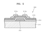
- FIG. 5 is a schematic cross-sectional view of an organic thin film transistor including the carbon thin film
- FIG. 6 is a graph illustrating Raman spectra of carbon thin films prepared in Examples 2, 4 and 5;
- FIG. 7 is a graph illustrating Raman spectra of carbon thin films prepared in Comparative Examples 1 to 3;
- FIG. 8 is a graph illustrating Raman spectra of carbon thin films prepared in Comparative Examples 4 to 6;
- FIG. 9 is a graph illustrating Raman spectra of carbon thin films prepared in Examples 6 and 7.
- FIG. 1 is a diagram for describing a method of preparing a carbon thin film according to an embodiment. Referring to FIG. 1 , the method of preparing a carbon thin film will be described.
- the substrate 11 may include a material that does not substantially react with a polymer layer 13 that will be formed on the substrate 11 and is not deformed or does not deteriorate at a high temperature.
- the substrate 11 may be any substrate that is commonly used in a semiconductor process.
- the substrate 11 may include silicon, a silicon oxide such as SiO 2 , a silicon nitride such as SiN, a semiconductor nitride such as GaN, metal foils such as copper foil, aluminum foil, nickel foil, and palladium foil, and stainless steel, a metal oxide, a highly ordered pyrolytic graphite (HOPG), hexagonal boron nitride (h-BN), a c-plane sapphire wafer, zinc sulfide (ZnS), a polymer substrate, or a combination of at least two of the foregoing.
- HOPG highly ordered pyrolytic graphite
- h-BN hexagonal boron nitride
- ZnS zinc sulfide
- the metal foil may include a material that has a high melting point and does not act as a catalyst capable of forming the carbon thin film such as aluminum foil, or a material acting as a catalyst capable of forming the carbon thin film such as copper foil and nickel foil.
- the metal oxide may include aluminum oxide, molybdenum oxide, magnesium oxide, and indium tin oxide
- the polymer substrate may include kapton foil, polyethersulphone (PES), polyacrylate (PAR), polyetherimide (PEI), polyethylene naphthalate (PEN), polyethylene terephthalate (PET), polyphenylene sulfide (PPS), polyallylate, polyimide, polycarbonate (PC), cellulose triacetate (TAC), cellulose acetate propionate (CAP), and the like, but is not limited thereto.
- the metal foil acting as a catalyst capable of forming the carbon thin film such as Cu, Ni, and Pd is used to form the substrate 11 in order to facilitate the carbonization of the polymer layer 13 , a step of forming a catalyst layer on the substrate 11 may not be performed.
- a carbon thin film may be formed without forming a catalyst layer on the substrate 11 (The catalyst layer will be described with reference to FIG. 2 ).
- the substrate 11 may have a single-layered structure including one material or a combination of at least two different materials or a multi-layered structure in which at least two layers, each of which includes a single material, are stacked.
- the substrate 11 may have a double layered structure including a silicon layer and a silicon oxide layer.
- Step 1 A in which the polymer layer 13 is formed on the substrate 11 is performed.
- Step 1 A is performed by using a coating process.
- a polymer of the polymer layer 13 may include an insulating polymer that includes carbon and hydrogen, has a thermal decomposition temperature of 600° C. or less, and includes a non-conjugated main chain.
- the polymer of the polymer layer 13 may include at least one selected from the group consisting of a repeating unit represented by Formula 1 below, a repeating unit represented by Formula 2 below, and a repeating unit represented by Formula 3 below.
- Y 1 may be N or C(R 11 ).
- Y 2 may be O, S, N(R 12 ), or C(R 13 )(R 14 ).
- Y 3 and Y 4 may be each independently N or C(R 15 ), and A 1 may be a substituted or unsubstituted C 6 -C 30 aryl group or a substituted or unsubstituted C 2 -C 30 heteroaryl group.
- R 1 to R 10 may be efficiently detached from the structures during a heat-treatment performed for forming the “carbon thin film” which will be described later.
- R 1 to R 10 may be each independently selected from the group consisting of a hydrogen atom (H), a nitro group (—NO 2 ), a cyano group (—CN), a hydroxyl group (—OH), a carboxyl group (—COOH), a halogen atom, a substituted or unsubstituted C 1 -C 30 alkyl group, a substituted or unsubstituted C 1 -C 30 alkoxy group, a substituted or unsubstituted C 6 -C 30 aryl group, a substituted or unsubstituted C 6 -C 30 arylalkyl group, a substituted or unsubstituted C 6 -C 30 aryloxy group, a substituted or unsubstituted C 2 -C 30 heteroaryl group, a substituted or unsubstituted C 2 -C 30 heteroarylalkyl group, a substituted or unsubstituted C 2 -C 30 heteroary
- R 1 to R 15 may be each independently selected from the group consisting of a hydrogen atom (H), a nitro group (—NO 2 ), a cyano group (—CN), a hydroxyl group (—OH), a carboxyl group (—COOH), a halogen atom, a C 1 -C 10 alkyl group, a C 1 -C 10 alkoxy group, and —N(Q 1 )(Q 2 ).
- Q 1 to Q 2 may be each independently selected from the group consisting of a hydrogen atom and a C 1 -C 10 alkyl group.
- R 1 to R 15 may be each independently selected from the group consisting of a hydrogen atom (H), a nitro group (—NO 2 ), a cyano group (—CN), a hydroxyl group (—OH), a carboxyl group (—COOH), a halogen atom, a methyl group, an ethyl group, a propyl group, a butyl group, a pentyl group, a hexyl group, a heptyl group, an octyl group, a methoxy group, an ethoxy group, a propoxy group, a butoxy group, a pentoxy group, and —NH 2 , but are not limited thereto.
- the substituent of the substituted C 6 -C 30 aryl group or the substituted C 2 -C 30 heteroaryl group may be selected from the group consisting of a nitro group (—NO 2 ), a cyano group (—CN), a hydroxyl group (—OH), a carboxyl group (—COOH), a halogen atom, a C 1 -C 30 alkyl group, a C 1 -C 30 alkoxy group, a C 6 -C 30 aryl group, a C 6 -C 30 arylalkyl group, a C 6 -C 30 aryloxy group, a C 2 -C 30 heteroaryl group, a C 2 -C 30 heteroarylalkyl group, a C 2 -C 30 heteroaryloxy group, a C 5 -C 20 cycloalkyl group
- the substituent may be selected from the group consisting of a nitro group (—NO 2 ), a cyano group (—CN), a hydroxyl group (—OH), a carboxyl group (—COOH), a halogen atom, a C 1 -C 10 alkyl group, and a C 1 -C 10 alkoxy group, but is not limited thereto.
- the polymer contained in the polymer layer 13 may include or consist of the repeating unit represented by Formula 1, wherein Y 1 is N.
- the polymer contained in the polymer layer 13 may include or consist of the repeating unit represented by Formula 1, wherein Y 1 is N, and R 1 to R 3 may be each independently selected from the group consisting of a hydrogen atom (H), a nitro group (—NO 2 ), a cyano group (—CN), a hydroxyl group (—OH), a carboxyl group (—COOH), a halogen atom, a methyl group, an ethyl group, a propyl group, a butyl group, a pentyl group, a hexyl group, a heptyl group, an octyl group, a methoxy group, an ethoxy group, a propoxy group, a butoxy group, a pentoxy group, and —NH 2 .
- R 1 to R 3 may be each independently selected from the group consisting of a hydrogen atom (H), a nitro group (—NO 2 ), a cyano group (—
- the polymer contained in the polymer layer 13 may also include or consist of the repeating unit represented by Formula 2, wherein Y 2 is O.
- the polymer contained in the polymer layer 13 may include or consist of the repeating unit represented by Formula 2, wherein Y 1 is O; R 7 may be selected from the group consisting of a hydrogen atom (H), a C 1 -C 10 alkyl group, and a C 1 -C 10 alkoxy group (e.g., a methoxy group, an ethoxy group, a propoxy group, a butoxy group, and a pentoxy group); and R 4 to R 6 may be each independently selected from the group consisting of a hydrogen atom (H), a nitro group (—NO 2 ), a cyano group (—CN), a hydroxyl group (—OH), a carboxyl group (—COOH), a halogen atom, a methyl group, an ethyl group, a propyl group, a butyl group, a pentyl group, a hexyl group, a heptyl group, an octyl
- the polymer contained in the polymer layer 13 may also include or consist of the repeating unit represented by Formula 3, wherein A 1 may be selected from the group consisting of a substituted or unsubstituted phenyl group, a substituted or unsubstituted pentalenyl group, a substituted or unsubstituted indenyl group, a substituted or unsubstituted naphthyl group, a substituted or unsubstituted azulenyl group, a substituted or unsubstituted heptalenyl group, a substituted or unsubstituted indacenyl group, a substituted or unsubstituted acenaphthyl group, a substituted or unsubstituted fluorenyl group, a substituted or unsubstituted phenalenyl group, a substituted or unsubstituted phenanthrenyl group, a substituted or unsubstitute
- a 1 may be a substituted or unsubstituted phenyl group, a substituted or unsubstituted naphthyl group, or a substituted or unsubstituted pyridinyl group, but is not limited thereto.
- the polymer contained in the polymer layer 13 may include at least one repeating unit selected from the group consisting of the repeating units represented by Formulae 11a to 13f:
- the polymer contained in the polymer layer 13 may be a polymer consisting of the repeating unit represented by Formula 11a, a polymer consisting of the repeating unit represented by Formula 12a, a polymer consisting of the repeating unit represented by Formula 12b, a polymer consisting of the repeating unit represented by Formula 13a, a polymer consisting of the repeating unit represented by Formula 13b, a polymer consisting of the repeating unit represented by Formula 13c, a polymer consisting of the repeating unit represented by Formula 13d, a polymer consisting of the repeating unit represented by Formula 13e, or a polymer consisting of the repeating unit represented by Formula 13f, but is not limited thereto.
- the polymer contained in the polymer layer 13 may be a polymer consisting of one of the repeating units represented by Formulae 1 to 3 or a copolymer including at least one of the repeating units represented by Formulae 1 to 3.
- the polymer contained in the polymer layer 13 may be a copolymer including at least one of the repeating unit represented by Formula 1, the repeating unit represented by Formula 2, the repeating unit represented by Formula 3, and further including a repeating unit selected from the group consisting of polyethylene (PE), polypropylene (PP), polybutene-1 (PB-1), poly 4-methyl-1-pentene, polyvinyl chloride (PVC), polyvinyl fluoride (PVF), polyvinyl amine (PVAm), polystyrene (PS), poly4-vinylphenol (PVP), poly(2-vinylnaphthalene), poly(1-vinylnaphthalene), poly 2-vinyl pyridine, poly 4-vinyl pyridine, polyisobutylene, polyvinylidene fluoride, polyvinylidene chloride, and polyacrylic acid.
- the polymer contained in the polymer layer 13 may be a copolymer of at least one of the repeating unit represented by Formula 1, the repeat
- the polymer contained in the polymer layer 13 may be polystyrene, polyacrylonitrile (PAN), polymethyl methacrylate, polyethyl methacrylate, or polyvinyl alcohol, but is not limited thereto.
- a weight average molecular weight (Mw) of the polymer contained in the polymer layer 13 may be in the range of 1,000 to 10,000,000, for example 10,000 to 1,000,000. If the weight average molecular weight (Mw) of the polymer contained in the polymer layer 13 is within the range described above, a first mixture that will be described below may have fluidity and/or viscosity suitable for a coating process, and a carbon thin film having excellent conductivity may be obtained.
- Step 1 A includes providing a first mixture including the polymer and a solvent or a second mixture including a precursor of the polymer and a solvent to the substrate 11 by using a coating process.
- the precursor is polymerized during a soft baking process and heat-treatment which will be described below, resulting in forming the polymer as described above.
- the first mixture and the second mixture may further include at least one additive selected from the group consisting of a cross-linking agent, an acid catalyst, a metal filler, a ceramic filler, and nanoparticles.
- the coating process may be spin-coating, inkjet printing, nozzle printing, dip coating, electrophoretic deposition, tape casting, screen printing, doctor blade coating, gravure printing, gravure offset printing, Langmuir-Blodgett (LB) technique, or layer-by-layer self-assembly, but is not limited thereto.
- the coating process may be spin-coating.
- the thickness of the polymer layer 13 may be controlled, so that the thickness of the carbon thin film 17 may also be controlled. According to the method of preparing a carbon thin film, the thickness of the carbon thin film may be controlled.
- a soft baking may optionally be performed in order to remove the solvent contained in the first mixture and/or the second mixture.
- the temperature range and time period for the soft baking may be controlled according to the polymer, the solvent, concentrations of the first mixture, and/or the second mixture.
- the thickness of the polymer layer 13 may be controlled by regulating the concentrations of the first mixture and the second mixture and may be in the range of 2 nm to 50 ⁇ m, for example, 2 nm to 1000 nm. If the thickness of the polymer layer 13 is within the range described above, a carbon thin film having a thickness greater than that of a graphene monolayer may be prepared, and the polymer layer 13 may have uniform quality.
- the prepared carbon thin film 17 may have a thickness in the range of 0.34 nm, which is similar to a thickness of a graphene monolayer, to 50 nm. Due to excellent transmittance of visible light, the prepared carbon thin film 17 may be used as a transparent electrode of a variety of displays. For example, the prepared carbon thin film 17 may be used as a wiring electrode by increasing the thickness of the polymer layer 13 to about 50 ⁇ m or greater.
- Step 1 B by which a protective layer 15 is formed on the polymer layer 13 is performed.
- the protective layer 15 prevents the polymer contained in the polymer layer 13 from being lost by degradation and/or calcination during the heat-treatment.
- the carbon thin film 17 may have excellent conductivity due to a plurality of domains having a graphene structure in which 6-membered carbon rings are fused with each other.
- the protective layer 15 may include a material having a melting point of 800° C. or higher.
- the protective layer 15 may include at least one selected from the group consisting of metal, a metal oxide, ceramic, a semiconductor oxide, and a semiconductor nitride.
- the protective layer 15 may include at least one selected from the group consisting of copper (Cu), nickel (Ni), palladium (Pd), gold (Au), silver (Ag), aluminum (Al), molybdenum (Mo), a copper oxide, a nickel oxide, a palladium oxide, an aluminum oxide, a molybdenum oxide, gallium nitride (GaN), silicon nitride (SiN), silicon oxide (SiO 2 ), and a combination of at least two of the foregoing.
- the thickness of the protective layer 15 may be in the range of 2 nm to 2000 nm, for example, 10 nm to 600 nm. If the thickness of the protective layer 15 is within the range described above, a uniform layer may be formed.
- the protective layer 15 may be formed by using any known method used to form a metal layer and/or a metal oxide layer, e.g., deposition.
- Step 1 C as a heat-treatment, is performed to carbonize the polymer layer 13 , resulting in preparing the carbon thin film 17 .
- the heat-treatment may be performed under conditions where the polymers contained in the polymer layer 13 are carbonized.
- the heat-treatment may be performed in an inert atmosphere, for example, in a nitrogen, argon, and/or hydrogen atmosphere, or in a vacuum atmosphere.
- hydrogen gas, methane gas, CF 4 gas, or the like may optionally be injected thereinto during the heat-treatment as impurity gas to modify a work function of the carbon thin film 17 by facilitating carbonization or inducing defects in the carbon thin film 17 .
- the heat-treatment may be performed at a temperature in the range of a thermal decomposition temperature of the polymer contained in the polymer layer 13 to 2500° C., for example, 600° C. to 1500° C., for 30 seconds to 5 days, for example 1 minute to 20 hours.
- the atmosphere, temperature range, and time period of the heat-treatment may vary according to the structure and content of the polymer contained in the polymer layer 13 .
- the polymer of the polymer layer 13 is carbonized, resulting in forming the carbon thin film 17 .
- the polymers consecutively bind to each other to form domains having a graphene-like structure.
- the protective layer 15 may be removed by increasing the temperature of the heat-treatment Step 1 C to greater than melting points of materials contained in the protective layer 15 .
- the method of preparing a carbon thin film may further include removing the protective layer 15 remaining on the carbon thin film 17 .
- the protective layer 15 remaining on the carbon thin film 17 may be removed using any known method used to remove a metal layer and/or a metal oxide layer.
- the protective layer 15 remaining on the carbon thin film 17 may be removed by washing the surface of the carbon thin film 17 with an etchant for a metal or a metal oxide.
- the protective layer 15 is formed of Ni, it may be removed using FeCl 3 (generally, 1 M in distilled water) or a marble reagent (generally, 50 ml of HCl:50 ml of distilled water:10 g of CuSO 4 solution).
- FeCl 3 generally, 1 M in distilled water
- a marble reagent generally, 50 ml of HCl:50 ml of distilled water:10 g of CuSO 4 solution.
- the method of preparing a carbon thin film is based on the coating process and heat-treating process, a cost-effective, stable, large-area, and two-dimensional carbon thin film 17 may be obtained according to the method of preparing a carbon thin film.
- the carbon thin film 17 may be efficiently controlled by regulating the concentrations of the first mixture and/or the second mixture, the carbon thin film 17 may have various sizes.
- the carbon thin film 17 may be patterned by patterning the protective layer 15 and the polymer layer 13 before performing Step 1 C, or patterning the carbon thin film 17 after performing Step 1 C and before separating the carbon thin film 17 from the substrate 11 . Because a variety of device assemblies may directly be disposed on the patterned carbon thin film 17 , the carbon thin film 17 may be efficiently applied to electrodes or wirings having various patterns.
- the patterning process may be performing using at least one method selected from the group consisting of photolithography, soft lithography, e-beam lithography, nanoimprint lithography, mold-assisted lithography, step and flash imprint lithography, dip pen lithography, microcontact printing, and inkjet printing.
- a patterning using a photoresist and a mask and/or a patterning using oxygen plasma may be used after performing Step 1 D (i.e., second heat-treatment).
- the carbon thin film 17 may be a graphite sheet, a graphene sheet (or film), a-few-layer graphene, and an amorphous carbon film.
- the graphene sheet may be a graphene monolayer having a thickness of 0.34 nm, a few-layer graphene in which 2 to 10 graphene monolayers are stacked, or a multilayer graphene in which more than 10 graphene monolayers are stacked.
- the carbon thin film 17 may be a graphene sheet.
- the carbon thin film 17 may be a few-layer graphene, but is not limited thereto.
- the carbon thin film 17 may have 50% or higher transmittance of visible light.
- the carbon thin film 17 may have excellent conductivity.
- the carbon thin film 17 may have a conductivity of 10 S/cm or greater.
- FIG. 2 is a diagram for describing a method of preparing a carbon thin film, according to another embodiment.
- the method described with reference to FIG. 2 is identical to the method of preparing a carbon thin film described with reference to FIG. 1 , except that a catalyst layer 32 is formed on a substrate 31 , and then a polymer layer 33 is formed on the catalyst layer 32 .
- the polymer layer 33 is formed on the catalyst layer 32 (Step 3 A), and a protective layer 35 is formed on the polymer layer 33 (Step 3 B), and then a carbon thin film 37 is formed by heat-treating (Step 3 C).
- the substrate 31 , the polymer layer 33 , the protective layer 35 , the carbon thin film 37 , Step 3 A, Step 3 B, and Step 3 C shown in FIG. 2 refer to the substrate 11 , the polymer layer 13 , the protective layer 15 , the carbon thin film 17 , Step 1 A, Step 1 B, and Step 1 C shown in FIG. 1 .
- the catalyst layer 32 may act as a catalyst for forming a graphene structure while the carbon thin film 37 is formed so as to increase domains of the graphene-like structure of the carbon thin film 37 .
- the catalyst layer 32 may include nickel (Ni), cobalt (Co), iron (Fe), gold (Au), aluminum (Al), chromium (Cr), copper (Cu), magnesium (Mg), molybdenum (Mo), rhodium (Rh), silicon (Si), tantalum (Ta), titanium (Ti), tungsten (W), uranium (U), vanadium (V), zirconium (Zr), and a combination of at least two of the foregoing.
- the thickness of the catalyst layer 32 may be in the range of 10 nm to 1000 nm, for example, 200 nm to 600 nm.
- the catalyst layer 32 may remain after heat-treating (Step 3 ) to form the carbon thin film 37 .
- the method may further include removing the catalyst layer 32 to separate the carbon thin film 37 from the substrate 31 .
- the method may further include stabilizing the polymer layer 33 by pre-heat-treating the polymer layer 33 before forming the protective layer 35 .
- the pre-heat-treatment at least one portion of the polymers contained in the polymer layers 13 and 33 may be converted into “stabilized polymer”.
- the pre-heat-treatment may be performed under conditions where at least one of intramolecular addition reaction and intramolecular double bond formation reaction occurs in the polymers contained in the polymer layers 13 and 33 .
- the conditions for the pre-heat-treatment may vary according to the structure, orientation, and the contents of the polymers contained in the polymer layers 13 and 33 , but the pre-heat-treatment may be performed, for example, at a temperature of 200° C. to 350° C. (e.g., 250° C. to 300° C.) and for 1 minute to 24 hours (e.g., 1 minute to 15 hours).
- the stabilized polymer contained in the polymer layers 13 and 33 includes a plurality of saturated or unsaturated 6-membered rings, wherein the saturated or unsaturated 6-membered rings may be fused with each other.
- the stabilized polymers may include at least one selected from the group consisting of a repeating unit represented by Formula 1a below and a repeating unit represented by Formula 1b below.
- the stabilized polymers may include at least one selected from the group consisting of a repeating unit represented by Formula 2a below, a repeating unit represented by Formula 2b below, and a repeating unit represented by Formula 2c below.
- polymers contained in the polymer layers 13 and 33 include the repeating unit represented by Formula 3, a double bond contained in a ring represented by A 1 of Formula 3 may contribute to the formation of the stabilized polymers in a similar manner as a —C ⁇ Y 2 — bond of Formula 2, but the present invention is not limited thereto.
- polyacrylonitrile represented by Formula 4 below
- PAN polyacrylonitrile
- an intramolecular addition reaction occurs between N of a cyano group of the polyacrylonitrile and C of an adjacent cyano group to form a single bond by the pre-heat-treatment as described above, resulting in producing a first stabilized polyacrylonitrile represented by Formula 4a below.
- an intermolecular double bond formation reaction occurs based on dehydrogenation, resulting in producing a second stabilized polyacrylonitrile represented by Formula 4b below.
- the stabilized polymer prepared by the pre-heat-treatment may include only the second stabilized polymer represented by Formula 4b or both of the first stabilized polymer represented by Formula 4a and the second stabilized polymer represented by Formula 4b. This may be controlled by conditions for the pre-heat-treatment.
- PAN polyacrylonitrile
- At least one portion of the polymer contained in the polymer layers 13 and 33 may be converted into stabilized polymers having a ladder structure with heat resistance by the pre-heat-treatment.
- the stabilized polymers are exposed to the heat-treatment for forming the carbon thin films 17 and 37 (Steps 1 C and 3 C of FIGS. 1 and 2 )
- the degradation of the polymers may be minimized.
- carbon thin films 17 and 37 may have excellent conductivity due to a plurality of domains having a graphene structure in which 6-membered carbon rings are fused with each other.
- the carbon thin films 17 and 37 including a plurality of first layers having the structure as shown in Formula 4d may be obtained.
- the plurality of first layers may be stacked in a second direction perpendicular to a first direction in which the first layers extend, but the present invention is not limited thereto.
- the catalyst layer 32 and/or the protective layers 15 and 35 may remain after forming the carbon thin films 17 and 37 and may be removed using an etchant.
- the carbon thin films 17 and 37 may directly be used on the substrates 11 and 31 on which the carbon thin films 17 and 37 are formed.
- the carbon thin films 17 and 37 formed on the substrates 11 and 31 are directly patterned to form carbon thin film electrode patterns on the substrates 11 and 31 .
- the carbon thin films 17 and 37 are separated from the substrates 11 and 31 on which the carbon thin films 17 and 37 are formed and transferred to another substrate such as a plastic substrate to prepare a flexible device.
- the transferring process may be performed by separating the carbon thin films 17 and 37 from the substrates 11 and 31 by contacting the carbon thin films 17 and 37 formed on the substrates 11 and 31 with an adhesive layer, such as polymethyl methacrylate (PMMA), polydimethylsiloxane (PDMS), and a thermal release tape, and contacting the carbon tin films 17 and 37 in contact with the adhesive layer with another substrate.
- an adhesive layer such as polymethyl methacrylate (PMMA), polydimethylsiloxane (PDMS), and a thermal release tape
- PMMA polymethyl methacrylate
- PDMS polydimethylsiloxane
- thermal release tape a thermal release tape
- the carbon thin films 17 and 37 may be applied to a variety of conductive layers.
- the carbon thin films 17 and 37 may be applied to electrodes, wirings, and channel layers of various electronics and electrochemical devices.
- the electronics may be inorganic light emitting diodes, organic light emitting diodes (OLEDs), inorganic solar cells, organic photovoltaic cells (OPVs), or inorganic thin film transistors, memories, electrochemical/bio sensors, RF devices, rectifiers, complementary metal oxide semiconductor (CMOS) devices, or organic thin film transistors (OTFT), and the electrochemical devices may be lithium batteries or fuel cells, but they are not limited thereto.
- FIG. 3 is a schematic cross-sectional view of an organic light-emitting diode 100 including the carbon thin film.
- the organic light-emitting diode 100 of FIG. 3 includes a first electrode 110 , a hole injection layer (HIL) 120 , a hole transport layer (HTL) 130 , an emission layer (EML) 140 , an electron transport layer (ETL) 150 , an electron injection layer (EIL) 160 , and a second electrode 170 .
- HIL hole injection layer
- HTL hole transport layer
- EML emission layer
- ETL electron transport layer
- EIL electron injection layer
- the first electrode 110 may be the carbon thin film as described above.
- the HIL 120 may be formed by using any known method selected from the group consisting of vacuum deposition, spin-coating, casting, LB technique, or the like.
- deposition conditions may vary according to a compound that is used to form the HIL 120 , and the structure and thermal properties of the HIL 120 to be formed.
- conditions for vacuum deposition may include a deposition temperature ranging from 100 to 500° C., a pressure ranging from 10 ⁇ 10 to 10 ⁇ 3 torr, and a deposition velocity ranging from 0.01 to 100 ⁇ /sec.
- coating conditions may vary according to a compound that is used to form the HIL 120 , and the structure and thermal properties of the HIL 120 to be formed.
- conditions for the spin-coating may include the coating speed ranging from 2000 to 5000 rpm, and a heat-treatment temperature for removing a solvent after coating ranging from 80 to 200° C.
- a material used to form the HIL 120 may be any known hole injecting material.
- the material include a phthalocyanine compound such as copper phthalocyanine, m-MTDATA represented by the following formula, TDATA represented by the following formula, 2T-NATA represented by the following formula, polyaniline/dodecylbenzenesulfonic acid (Pani/DBSA), poly(3,4-ethylenedioxythiophene)/poly(4-styrenesulfonate) (PEDOT/PSS), polyaniline/camphor sulfonicacid (Pani/CSA), and (polyaniline)/poly(4-styrenesulfonate) (PANI/PSS), but are not limited thereto.
- a phthalocyanine compound such as copper phthalocyanine
- m-MTDATA represented by the following formula
- TDATA represented by the following formula
- 2T-NATA represented by the following formula
- the thickness of the HIL 120 may be in the range of about 10 to about 10000 ⁇ , for example, about 100 to about 1000 ⁇ . When the thickness of the HIL 120 is within the range described above, the HIL 120 may have excellent hole injecting properties without an increase in driving voltage.
- the HTL 130 may be formed by using any known method selected from the group consisting of vacuum deposition, spin-coating, casting, LB technique, or the like.
- the deposition and coating conditions may be similar to those for the formation of the HIL 120 , although the deposition and coating conditions may vary according to a compound that is used to form the HTL 130 , and the structure and thermal properties of the HTL 130 to be formed.
- a material used to form the HTL 130 may be any known hole transporting material.
- the material include an amine derivative having an aromatic condensation ring such as N,N′-di(1-naphthyl)-N,N′-diphenylbenzidine (NPB), N-phenylcarbazole, and N,N′-bis(3-methylphenyl)-N,N′-diphenyl-[1,1-biphenyl]-4,4′-diamine (TPD), and a triphenylamine-based material such as 4,4′,4′′-tris(N-carbazolyl)triphenylamine (TCTA).
- TCTA may not only transport holes but also inhibit excitons from being diffused from the EML 140 .
- the thickness of the HTL 130 may be in the range of about 50 to about 1,000 ⁇ , for example, about 100 to about 600 ⁇ . When the thickness of the HTL 130 is within this range, the HTL 130 may have excellent hole transporting properties without an increase in driving voltage.
- the EML 140 may be formed by using any known method selected from the group consisting of vacuum deposition, spin-coating, casting, LB technique, or the like.
- the deposition and coating conditions may be similar to those for the formation of the HIL 120 , although the deposition and coating conditions may vary according to a compound that is used to form the EML 140 , and the structure and thermal properties of the EML 140 to be formed.
- the EML 140 may be formed of an emitting material or may include a host and a dopant.
- Examples of the host include Alq 3 , 4,4′-N,N′-dicarbazole-biphenyl (CBP), 9,10-di(naphthalene-2-yl)anthracene (ADN), TCTA, 1,3,5-tris(N-phenylbenzimidazole-2-yl)benzene (TPBI), 3-tert-butyl-9,10-di(naphtha-2-yl)anthracene (TBADN), E3 (refer to the following formula), and BeBq 2 (refer to the following formula), but are not limited thereto.
- CBP 4,4′-N,N′-dicarbazole-biphenyl
- ADN 9,10-di(naphthalene-2-yl)anthracene
- TCTA 1,3,5-tris(N-phenylbenzimidazole-2-yl)benzene
- TPBI 1,3,5-tris(N-phenylbenzimid
- red dopants examples include PtOEP, Ir(piq) 3 , and Btp 2 Ir(acac), but are not limited thereto.
- Examples of known green dopants include Ir(ppy) 3 (where “ppy” denotes phenylpyridine), Ir(ppy) 2 (acac), Ir(mpyp) 3 , and C545T, but are not limited thereto.
- blue dopants examples include F 2 Irpic, (F 2 ppy) 2 Ir(tmd), Ir(dfppz) 3 , terfluorene, 4,4′-bis(4-di-p-tolylaminostyryl)biphenyl (DPAVBi), and 2,5,8,11-tetra-t-butyl pherylene (TBP), but are not limited thereto.
- the thickness of the EML 140 may be in the range of about 100 to about 1,000 ⁇ , for example, about 100 to about 600 ⁇ . When the thickness of the EML 140 is within the range described above, the EML 140 may have excellent light-emitting characteristics without an increase in driving voltage.
- a hole blocking layer prevents diffusion of triplet excitons or holes of the EML 140 (if, the EML 140 includes a phosphorescent compound) into a second electrode.
- the HBL may be formed on the EML 140 by using any known method such as vacuum deposition, spin-coating, casting, and LB technique.
- the deposition and coating conditions may be similar to those for the formation of the HIL 120 , although the deposition and coating conditions may vary according to a compound that is used to form the HBL, and the structure and thermal properties of the HBL to be formed.
- a material used to form the HBL may be any known hole blocking material.
- oxadiazole derivatives, triazole derivatives, and phenanthroline derivatives may be used to form the HBL.
- the thickness of the HBL may be in a range of about 50 to about 1,000 ⁇ , for example, about 100 to about 300 ⁇ . When the thickness of the HBL is within the range described above, the HBL may have excellent hole blocking properties without an increase in driving voltage.
- the ETL 150 may be formed by using any known method selected from the group consisting of vacuum deposition, spin-coating, casting, LB technique, or the like.
- the deposition and coating conditions may be similar to those for the formation of the HIL 120 , although the deposition and coating conditions may vary according to a compound that is used to form the ETL 150 , and the structure and thermal properties of the ETL 150 to be formed.
- a material used to form the ETL 150 may be any known electron transporting material, for example, tris(8-quinolinorate)aluminum (Alq 3 ), TAZ, 4,7-diphenyl-1,10-phenanthroline (Bphen), BCP, BeBq 2 , and BAlq.
- the thickness of the ETL 150 may be in the range of about 100 to about 1,000 ⁇ , for example, about 200 to about 500 ⁇ . When the thickness of the ETL 150 is within the range described above, the ETL 150 may have excellent electron transporting properties without an increase in driving voltage.
- the EIL 160 may be formed on the ETL 150 .
- a material used to form the EIL 160 may be any known electron injecting material such as LiF, NaCl, CsF, Li 2 O, BaO, and BaF 2 .
- the deposition conditions may be similar to those for the formation of the HIL 120 , although the deposition conditions may vary according to a compound that is used to form the EIL 160 .
- the thickness of the EIL 160 may be in the range of about 1 to about 100 ⁇ , for example, about 5 to about 50 ⁇ . When the thickness of the EIL 160 is within the range described above, the EIL 160 may have satisfactory electron injecting properties without an increase in driving voltage.
- the second electrode 170 may be a cathode, which is an electron injecting electrode.
- a low work function material such as metal, an alloy, an electrically conductive compound, or any combination thereof may be used to form the second electrode 170 .
- the second electrode 170 may be formed of lithium (Li), magnesium (Mg), aluminum (Al), aluminum (Al-lithium (Li), calcium (Ca), magnesium (Mg)-indium (In), magnesium (Mg)-silver (Ag), or the like.
- ITO, IZO, or the like may also be used to prepare a top-emission type light-emitting diode.
- the organic light-emitting diode 100 including the carbon thin film may have a first electrode (carbon thin film)/HIL (PEDOT, 50 nm)/HTL (NPB, 20 nm)/EML (BeBq2:C545T, 30 nm)/ETL (BeBq2, 20 nm)/EIL (LiF, 1 nm)/second electrode (Al, 150 nm) structure, but is not limited thereto.
- the first electrode 110 of the organic light-emitting diode 100 may be prepared by using the method of preparing a carbon thin film as described above, the first electrode 110 has excellent electrical properties and may be prepared in a cost-effective manner.
- FIG. 4 is a schematic cross-sectional view of an organic photovoltaic cell 200 including the carbon thin film.
- the organic photovoltaic cell 200 of FIG. 4 includes a first electrode 210 , a hole collecting buffer layer 220 , a hetero-junction layer 230 , an electron accepting (or collecting) layer 240 , and a second electrode 250 .
- Light that arrives at the organic photovoltaic cell 200 splits into holes and electrons in the hetero-junction layer 230 .
- the electrons move to the second electrode 250 via the electron accepting layer 240
- the holes move to the first electrode 210 via the hole collecting buffer layer 220 .
- the first electrode 210 may be the carbon thin film as described above.
- the hole collecting buffer layer 220 may include a material capable of accepting holes, for example, the materials used to form the HIL 120 and the HTL 130 of the organic light-emitting diode 100 as described above.
- the hetero-junction layer 230 may include a material capable of splitting light into holes and electrons.
- the hetero-junction layer 230 may include a p-type organic semiconductor material or an n-type organic semiconductor material.
- the hetero-junction layer 230 may include poly(3-hexylthiophene) and phenyl-C61-butyric acid methyl ester (PCMB), but is not limited thereto.
- the electron accepting layer 240 may include a material capable of accepting electrons, for example, the material used to form the EIL 160 of the organic light-emitting diode 100 as described above.
- the second electrode 250 may be a cathode, which is an electron injecting electrode.
- a low work function material such as metal, an alloy, an electrically conductive compound, or any combination thereof may be used to form the second electrode 250 .
- the second electrode 250 may be formed of lithium (Li), magnesium (Mg), aluminum (Al), aluminum (Al-lithium (Li), calcium (Ca), magnesium (Mg)-indium (In), magnesium (Mg)-silver (Ag), or the like.
- the organic photovoltaic cell 200 including the carbon thin film may have a first electrode (carbon thin film)/buffer layer (PEDOT, 35 nm)/hetero-junction layer (P 3 HT:PCBM, 210 nm)/electron accepting layer (BaF 2 , 1 nm)/second electrode (Al, 100 nm) structure, but is not limited thereto.
- FIG. 5 is a schematic cross-sectional view of an organic thin film transistor 300 including the carbon thin film.
- the organic thin film transistor 300 of FIG. 5 includes a substrate 311 , a gate electrode 312 , an insulating layer 313 , an organic semiconductor layer 315 , and source and drain electrodes 314 a and 314 b . At least one of the gate electrode 312 , the organic semiconductor layer 315 , and the source and drain electrodes 314 a and 314 b may be the carbon thin film as described above.
- the substrate 311 may be any substrate that is commonly used in electronics, and may be a glass substrate or a transparent plastic substrate with excellent transparency, surface smoothness, ease of handling, and water resistance.
- the gate electrode 312 may be formed on the substrate 311 with a predetermined pattern.
- the gate electrode 312 may be formed of a metal such as gold (Au), silver (Ag), copper (Cu), nickel (Ni), platinum (Pt), palladium (Pd), aluminum (Al), and molybdenum (Mo), or a metal alloy such as Al:Nd and Mo:W, but is not limited thereto.
- the gate electrode 312 may also be the carbon thin film as described above.
- the insulating layer 313 is formed on the gate electrode 312 to cover the gate electrode 312 .
- the insulating layer 313 may include an inorganic material such as a metal oxide or metal nitride, an organic material such as an insulating organic polymer, or various other materials.
- the organic semiconductor layer 315 is formed on the insulating layer 313 .
- the organic semiconductor layer 315 may be the carbon thin film as described above.
- the organic semiconductor layer 315 may include pentacene, tetracene, anthracene, naphthalene, ⁇ -6-thiophene, ⁇ -4-thiophene, perylene and derivatives thereof, rubrene and derivatives thereof, coronene and derivatives thereof, perylene tetracarboxylic diimide and derivatives thereof, perylene tetracarboxylic dianhydride and derivatives thereof, polythiophene and derivatives thereof, poly(p-phenylene vinylene) and derivatives thereof, poly(p-phenylene) and derivatives thereof, polyfluorene and derivatives thereof, polythiophenevinylene and derivatives thereof, polythiophene-hetero ring aromatic copolymer and derivatives thereof, oligoacene of naphthalene and derivatives thereof
- the source and drain electrodes 314 a and 314 b are respectively formed on the organic semiconductor layer 315 .
- the source and drain electrodes 314 a and 314 b may overlap with a portion of the gate electrode 312 as shown in FIG. 6 , but are not limited thereto.
- the source and drain electrodes 314 a and 314 b may be the carbon thin film as described above.
- the source and drain electrodes 314 a and 314 b may include a noble metal having a work function of 5.0 eV or more, for example, gold (Au), palladium (Pd), platinum (Pt), nickel (Ni), rhodium (Rh), ruthenium (Ru), iridium (Ir), osmium (Os), or a combination of at least two of the foregoing in consideration of a work function of the material used to form the organic semiconductor layer 315 .
- a noble metal having a work function of 5.0 eV or more for example, gold (Au), palladium (Pd), platinum (Pt), nickel (Ni), rhodium (Rh), ruthenium (Ru), iridium (Ir), osmium (Os), or a combination of at least two of the foregoing in consideration of a work function of the material used to form the organic semiconductor layer 315 .
- the organic thin film transistor 300 may have a substrate/gate electrode/insulating layer/organic semiconductor layer (carbon thin film)/source and drain electrodes (Au, thicker than 10 nm) structure.
- the organic thin film transistor 300 may also have a substrate/gate electrode/insulating layer/organic semiconductor layer (pentacene)/source and drain electrodes (carbon thin film) structure.
- the second electrode 170 of the organic light-emitting diode 100 of FIG. 3 may be the carbon thin film according to the material used to form the first electrode 10 .
- FIG. 5 shows a bottom-gate type organic thin film transistor, organic thin film transistors having various structures such as a top-gate type organic thin film transistor may also be used.
- the carbon thin film according to the current embodiment may also be used to form electrodes and used as active materials in electronics such as memories, electrochemical/bio sensors, RF devices, rectifiers, and complementary metal oxide semiconductor (CMOS) devices, or electrochemical devices such as lithium batteries and fuel cells.
- CMOS complementary metal oxide semiconductor
- a silicon substrate (2.0 cm ⁇ 2.0 cm) on which a silicon oxide layer having a thickness of 300 nm is formed was prepared and the surface of the silicon oxide layer was hydrophilically modified by treating the surface of the silicon oxide layer with UV light/ozone for 30 minutes.
- a 2 wt % solution prepared by dissolving polystyrene (weight average molecular weight (Mw): 130000 g/mol, manufactured by Sigma-Aldrich) in dimethylformamide (DMF, manufactured by DAE JUNG Chemicals) solvent was spin coated on the silicon oxide layer, and baked at 100° C. for 3 minutes to remove the solvent, resulting in forming a polystyrene layer having a thickness of 10 nm.
- Nickel (Ni) was deposited on the polystyrene layer to form a Ni protective layer having a thickness of 50 nm, and then the substrate was disposed in a quartz tube and installed in a furnace.
- the substrate was heat-treated at 1000° C. for 1 minute using a halogen lamp heat source while uniformly flowing argon (Ar) gas (50 sccm) and hydrogen gas (10 sccm) in the quartz tube.
- the quartz tube including the substrate was separated from the furnace and naturally cooled. Then, the carbon thin film was separated from the substrate.
- the carbon thin film has a size of 2.0 cm ⁇ 2.0 cm and a thickness of 10 nm. Conductivity of the carbon thin film measured using a 4-point probe was 95 S/cm.
- a carbon thin film was obtained in the same manner as in Example 1, except that polyacrylonitrile (weight average molecular weight (Mw): 150000 g/mol, manufactured by Sigma-Aldrich) was used instead of the polystyrene.
- Conductivity of the carbon thin film measured using a 4-point probe was 100 S/cm.
- a carbon thin film was obtained in the same manner as in Example 1, except that polymethyl methacrylate (number average molecular weight (Mn): 130000 g/mol) was used instead of the polystyrene.
- Conductivity of the carbon thin film measured using a 4-point probe was 105 S/cm.
- a carbon thin film was obtained in the same manner as in Example 2, except that the thickness of the Ni protective layer was 25 nm instead of 50 nm. Conductivity of the carbon thin film measured using a 4-point probe was 25 S/cm.
- a carbon thin film was obtained in the same manner as in Example 2, except that the thickness of the Ni protective layer was 10 nm instead of 50 nm. Conductivity of the carbon thin film measured using a 4-point probe was 10 S/cm.
- Example 2 An experiment was performed in the same manner as in Example 1, except that a Ni layer having a thickness of 400 nm was formed on a silicon oxide layer, a polystyrene layer was formed thereon, and a Ni protective layer was not formed on the polystyrene layer.
- Example 2 An experiment was performed in the same manner as in Example 2, except that a Ni layer having a thickness of 400 nm was formed on a silicon oxide layer, a polyacrylonitrile layer was formed thereon, and a Ni protective layer was not formed on the polyacrylonitrile layer.
- Example 3 An experiment was performed in the same manner as in Example 3, except that a Ni layer having a thickness of 400 nm was formed on a silicon oxide layer, a polymethyl methacrylate layer was formed thereon, and a Ni protective layer was not formed on the polymethyl methacrylate layer.
- a silicon substrate (2.0 cm ⁇ 2.0 cm) on which a silicon oxide layer having a thickness of 300 nm is formed was prepared and the surface of the silicon oxide layer was hydrophilically modified by treating the surface of the silicon oxide layer with UV light/ozone for 30 minutes.
- a 2 wt % solution prepared by dissolving polyacetylonitrile (weight average molecular weight (Mw): 15,000 g/mol) in DMF solvent was spin coated on the silicon oxide layer, and baked at 160° C. for 3 minutes to remove the solvent, resulting in forming a polyacetylonitrile layer having a thickness of 25 nm.
- the polyacetylonitrile layer was pre-heat-treated at 250° C. under atmospheric conditions for 10 hours so that at least one portion of the polyacetylonitrile contained in the polyacetylonitrile layer was converted into stabilized polyacetylonitrile.
- Ni was deposited on the polyacetylonitrile layer to form a Ni protective layer having a thickness of 300 nm, and then the substrate was disposed in a quartz tube and installed in a furnace.
- the substrate was heat-treated at 600° C. for 3 hours using a halogen lamp heat source while uniformly flowing argon (Ar) gas (50 sccm) and hydrogen gas (10 sccm) in the quartz tube.
- Ar argon
- the quartz tube including the substrate was separated from the furnace and naturally cooled. Then, the carbon thin film was separated from the substrate.
- the carbon thin film has a size of 2.0 cm ⁇ 2.0 cm and a thickness of 10 nm. Conductivity of the carbon thin film measured using a 4-point probe was 100 S/cm.
- a carbon thin film having a size of 2.0 cm ⁇ 2.0 cm and a thickness of 5 nm was obtained in the same manner as in Example 6, except that the heat-treatment was performed at 1000° C. for 15 minutes.
- Conductivity of the carbon thin film measured using a 4-point probe was 110 S/cm.
- a carbon thin film having a size of 2.0 cm ⁇ 2.0 cm and a thickness of 10 nm was obtained in the same manner as in Example 6, except that a copper (Cu) protective layer having a thickness of 300 nm was formed instead of the Ni protective layer having a thickness of 300 nm.
- Conductivity of the carbon thin film measured using a 4-point probe was 10 S/cm.
- a carbon thin film having a size of 2.0 cm ⁇ 2.0 cm and a thickness of 20 nm was obtained in the same manner as in Example 6, except that the heat-treatment was performed at 1500° C. for 10 hours.
- Conductivity of the carbon thin film measured using a 4-point probe was 200 S/cm.
- a carbon thin film having a size of 2.0 cm ⁇ 2.0 cm and a thickness of 10 nm was obtained in the same manner as in Example 6, except that a polymethyl methacrylate layer (weight average molecular weight (Mw) of polymethyl methacrylate: 15,000) was used instead of the polyacrylonitrile layer.
- Conductivity of the carbon thin film measured using a 4-point probe was 95 S/cm.
- Raman spectra of carbon thin films prepared according to Examples 2, 4, and 5 were measured using a SENTERRA Dispersive Raman Microscope manufactured by BRUKER, and the results are shown in FIG. 6 .
- Raman spectra were obtained using a 50 ⁇ objective lens and a laser having a wavelength of 532 nm at room temperature.
- FIG. 7 is a graph illustrating Raman spectra of carbon thin films obtained in Comparative Examples 1 to 3.
- FIG. 8 is a graph illustrating Raman spectra of carbon thin films obtained in Comparative Examples 4 to 6. Referring to FIGS. 6 to 8 , the carbon thin films prepared in Examples 2, 4, and 5 show peaks of characteristics of graphene, while the carbon thin films prepared in Comparative Examples 1 to 6 do not show peaks of the characteristics of graphene.
- Raman spectra of carbon thin films prepared according to Examples 6 and 7 were measured using a SENTERRA Dispersive Raman Microscope manufactured by BRUKER, and the results are shown in FIG. 9 .
- Raman spectra were obtained using a 50 ⁇ objective lens and a laser having a wavelength of 532 nm at room temperature.
- the carbon thin film prepared in Example 6 shows a Raman shift value of about 1362 cm ⁇ 1 to 1597 cm ⁇ 1 and a strong broad band in FIG. 9 , it can be seen that the carbon thin film is amorphous carbon thin film. These properties may be caused by the temperature of the heat-treatment in Example 6. According to the Raman spectrum of the carbon thin film, the carbon thin film prepared in Example 7 is graphene. In this regard, a peak the carbon thin film of Example 7 at 1346 cm ⁇ 1 is derived from a remaining CN group or a defect of the carbon thin film.
- a cost-effective, stable, large-area, and two-dimensional carbon thin film may be efficiently prepared.
- the carbon thin film may have excellent conductivity, and thus it may be applied to various conductive electrodes or wirings.
Abstract
Description


Claims (19)

Applications Claiming Priority (4)
| Application Number | Priority Date | Filing Date | Title |
|---|---|---|---|
| KR20100071062 | 2010-07-22 | ||
| KR10-2010-0071062 | 2010-07-22 | ||
| KR10-2011-0070032 | 2011-07-14 | ||
| KR1020110070032A KR101271827B1 (en) | 2010-07-22 | 2011-07-14 | Method of preparing carbon thin film |
Publications (2)
| Publication Number | Publication Date |
|---|---|
| US20120021250A1 US20120021250A1 (en) | 2012-01-26 |
| US9159924B2 true US9159924B2 (en) | 2015-10-13 |
Family
ID=45443674
Family Applications (1)
| Application Number | Title | Priority Date | Filing Date |
|---|---|---|---|
| US13/187,671 Expired - Fee Related US9159924B2 (en) | 2010-07-22 | 2011-07-21 | Method of preparing carbon thin film, electronics comprising carbon thin film, and electrochemical device comprising carbon thin film |
Country Status (5)
| Country | Link |
|---|---|
| US (1) | US9159924B2 (en) |
| JP (1) | JP5620348B2 (en) |
| KR (1) | KR101271827B1 (en) |
| CN (1) | CN102515135B (en) |
| DE (1) | DE102011052041A1 (en) |
Cited By (6)
| Publication number | Priority date | Publication date | Assignee | Title |
|---|---|---|---|---|
| EP3334688A4 (en) * | 2015-08-14 | 2019-05-08 | Commonwealth Scientific and Industrial Research Organisation | Graphene synthesis |
| WO2022185166A1 (en) | 2021-03-04 | 2022-09-09 | Crystallyte Co., Ltd. | A process for growing a film of a metal-carbon nanomaterial composite with 1d, 2d, or 3d structure and/or a mixture thereof on a metal substrates |
| US11624723B2 (en) | 2016-09-16 | 2023-04-11 | Eastman Chemical Company | Biosensor electrodes prepared by physical vapor deposition |
| US11630075B2 (en) | 2016-09-16 | 2023-04-18 | Eastman Chemical Company | Biosensor electrodes prepared by physical vapor deposition |
| US11835481B2 (en) | 2016-06-15 | 2023-12-05 | Eastman Chemical Company | Physical vapor deposited biosensor components |
| US11881549B2 (en) | 2017-06-22 | 2024-01-23 | Eastman Chemical Company | Physical vapor deposited electrode for electrochemical sensors |
Families Citing this family (54)
| Publication number | Priority date | Publication date | Assignee | Title |
|---|---|---|---|---|
| CN102119363B (en) * | 2008-08-05 | 2015-10-21 | 斯莫特克有限公司 | For the high-aspect-ratio template of photoetching, the method making same template and the application of this template in nanoscale substrate perforation |
| WO2011087301A2 (en) * | 2010-01-15 | 2011-07-21 | 성균관대학교산학협력단 | Graphene protective film serving as a gas and moisture barrier, method for forming same, and use thereof |
| KR101348925B1 (en) * | 2012-03-15 | 2014-01-10 | 한국수력원자력 주식회사 | Fabrication method of organic material-derived graphene using radiation technique and the fabrication of the graphene using the same |
| JP6110695B2 (en) * | 2012-03-16 | 2017-04-05 | 株式会社半導体エネルギー研究所 | Light emitting device |
| KR101975852B1 (en) * | 2012-04-14 | 2019-05-07 | 세종대학교산학협력단 | Laminated body, electrionic device comprising the same and method for preparing the same |
| WO2014011294A2 (en) * | 2012-04-14 | 2014-01-16 | Northeastern University | Flexible and transparent supercapacitors and fabrication using thin film carbon electrodes with controlled morphologies |
| JP2015525186A (en) * | 2012-05-24 | 2015-09-03 | ビーエーエスエフ ソシエタス・ヨーロピアBasf Se | Graphene nanoribbons with controlled modification |
| CN102664218B (en) * | 2012-05-29 | 2014-06-25 | 哈尔滨工业大学 | Method for preparing flexible optical detector on basis of two-dimensional functional material |
| KR101950474B1 (en) * | 2012-08-22 | 2019-02-21 | 삼성디스플레이 주식회사 | Organic light emitting diode |
| KR101878754B1 (en) | 2012-09-13 | 2018-07-17 | 삼성전자주식회사 | Method of manufacturing large area gallium nitride substrate |
| KR101993767B1 (en) * | 2012-10-17 | 2019-07-01 | 한국전자통신연구원 | graphene nanoribbon sensor |
| KR101427818B1 (en) | 2012-10-29 | 2014-08-08 | 한국과학기술연구원 | Carbon materials based on organic nano film using thermal evaporation and method for preparing the same |
| US9561603B2 (en) | 2013-01-03 | 2017-02-07 | Elwha, Llc | Nanoimprint lithography |
| WO2014107524A1 (en) * | 2013-01-03 | 2014-07-10 | Elwha Llc | Nanoimprint lithography |
| US9962863B2 (en) | 2013-01-03 | 2018-05-08 | Elwha Llc | Nanoimprint lithography |
| US9302424B2 (en) | 2013-01-03 | 2016-04-05 | Elwha, Llc | Nanoimprint lithography |
| KR101425376B1 (en) | 2013-02-12 | 2014-08-01 | 한국과학기술연구원 | Large-area carbon nanomesh from polymer and method of preparing the same |
| KR20140125003A (en) * | 2013-04-17 | 2014-10-28 | 삼성디스플레이 주식회사 | Flexible display device and manufacturing method thereof |
| CN103236469A (en) * | 2013-04-22 | 2013-08-07 | 哈尔滨工业大学 | Method for preparing gallium telluride two-dimensional structural material and method for producing flexible transparent two-dimensional structural gallium telluride optical detector |
| JP6360043B2 (en) * | 2013-04-26 | 2018-07-18 | 株式会社長町サイエンスラボ | Structure having DLC layer and method for generating DLC layer |
| JP6264090B2 (en) * | 2013-07-31 | 2018-01-24 | 株式会社リコー | FIELD EFFECT TRANSISTOR AND METHOD FOR MANUFACTURING FIELD EFFECT TRANSISTOR |
| EP2854204B1 (en) | 2013-09-30 | 2017-06-14 | Samsung Electronics Co., Ltd | Composite, carbon composite including the composite, electrode, lithium battery, electroluminescent device, biosensor, semiconductor device, and thermoelectric device including the composite and/or the carbon composite |
| KR102062353B1 (en) * | 2013-10-16 | 2020-01-06 | 엘지디스플레이 주식회사 | Organic light emitting device and method of fabricating the same |
| CA2847462A1 (en) * | 2013-10-28 | 2015-04-28 | Institut National De La Recherche Scientifique | Method of producing a graphene coating on a stainless steel surface |
| US9505624B2 (en) * | 2014-02-18 | 2016-11-29 | Corning Incorporated | Metal-free CVD coating of graphene on glass and other dielectric substrates |
| CN104167496B (en) * | 2014-08-01 | 2018-02-23 | 上海和辉光电有限公司 | Inversion type top emitting device and preparation method thereof |
| CN104157791A (en) * | 2014-08-05 | 2014-11-19 | 京东方科技集团股份有限公司 | OLED (Organic Light Emitting Diode) display device and manufacturing method thereof as well as display device |
| CN104276566B (en) * | 2014-09-09 | 2016-09-14 | 深圳市本征方程石墨烯技术股份有限公司 | A kind of Graphene and preparation method thereof |
| KR101630070B1 (en) * | 2014-10-08 | 2016-06-14 | 경희대학교 산학협력단 | Graphene and method for growing of graphene using spontaneous pattern transfer |
| KR20180048641A (en) * | 2015-09-02 | 2018-05-10 | 도쿄엘렉트론가부시키가이샤 | Manufacturing method of graphene, manufacturing device of graphene, and manufacturing method of electronic device |
| CN106082164B (en) * | 2016-06-09 | 2018-03-27 | 周虎 | A kind of carbon film and its production method and production equipment |
| US10332693B2 (en) | 2016-07-15 | 2019-06-25 | Nanotek Instruments, Inc. | Humic acid-based supercapacitors |
| US11254616B2 (en) | 2016-08-04 | 2022-02-22 | Global Graphene Group, Inc. | Method of producing integral 3D humic acid-carbon hybrid foam |
| US10731931B2 (en) | 2016-08-18 | 2020-08-04 | Global Graphene Group, Inc. | Highly oriented humic acid films and highly conducting graphitic films derived therefrom and devices containing same |
| US10014519B2 (en) | 2016-08-22 | 2018-07-03 | Nanotek Instruments, Inc. | Process for producing humic acid-bonded metal foil film current collector |
| US10597389B2 (en) | 2016-08-22 | 2020-03-24 | Global Graphene Group, Inc. | Humic acid-bonded metal foil film current collector and battery and supercapacitor containing same |
| US20180061517A1 (en) * | 2016-08-30 | 2018-03-01 | Nanotek Instruments, Inc. | Highly Conductive Graphitic Films and Production Process |
| US10647595B2 (en) | 2016-08-30 | 2020-05-12 | Global Graphene Group, Inc. | Humic acid-derived conductive foams and devices |
| US10584216B2 (en) | 2016-08-30 | 2020-03-10 | Global Graphene Group, Inc. | Process for producing humic acid-derived conductive foams |
| US10593932B2 (en) | 2016-09-20 | 2020-03-17 | Global Graphene Group, Inc. | Process for metal-sulfur battery cathode containing humic acid-derived conductive foam |
| KR101908036B1 (en) * | 2016-10-28 | 2018-10-15 | 울산과학기술원 | Preparing method of high purity graphene using polyamic acid |
| US10978701B2 (en) | 2016-11-18 | 2021-04-13 | Samsung Electronics Co., Ltd. | Porous silicon composite cluster structure, method of preparing the same, carbon composite using the same, and electrode, lithium battery, and device each including the same |
| US10304234B2 (en) * | 2016-12-01 | 2019-05-28 | Disney Enterprises, Inc. | Virtual environment rendering |
| KR102620962B1 (en) * | 2016-12-07 | 2024-01-03 | 엘지디스플레이 주식회사 | Organic light emitting diode display and method for fabricating the same |
| JP6845568B2 (en) * | 2017-04-03 | 2021-03-17 | 学校法人 名城大学 | Graphene substrate and its manufacturing method |
| KR102227809B1 (en) | 2017-05-04 | 2021-03-15 | 주식회사 엘지화학 | Negative electrode active material, negative electrode comprising the negative electrode active material, lithium secondarty battery comprising the negative electrode and method for preparing the negative electrode active material |
| US10707477B2 (en) * | 2017-09-15 | 2020-07-07 | Dyson Technology Limited | High energy density multilayer battery cell with thermally processed components and method for making same |
| TWI631741B (en) | 2017-10-19 | 2018-08-01 | 元太科技工業股份有限公司 | Driving substrate |
| KR102013896B1 (en) * | 2018-03-29 | 2019-08-23 | 조인셋 주식회사 | Separator and Method for burning several green sheets unit using the same |
| KR102153100B1 (en) * | 2018-06-07 | 2020-09-07 | 재단법인 나노기반소프트일렉트로닉스연구단 | Graphene laminate, method for preparing the same, and organic electronic device comprising the same |
| KR20200047879A (en) | 2018-10-25 | 2020-05-08 | 삼성전자주식회사 | Porous silicon-containing composite, carbon composite using the same, and electrode, lithium battery, and electronic device each including the same |
| CN109712742B (en) * | 2018-12-17 | 2021-01-01 | 中国科学院合肥物质科学研究院 | Graphene crystal film with high conductivity and preparation method thereof |
| KR102218068B1 (en) * | 2019-02-22 | 2021-02-19 | 재단법인 나노기반소프트일렉트로닉스연구단 | Graphene laminate including flexible substrate, method for preparing the same, and organic electronic device comprising the same |
| CN114577659B (en) * | 2022-01-26 | 2024-02-06 | 株洲科能新材料股份有限公司 | Method for detecting gallium content in gallium nitride material |
Citations (20)
| Publication number | Priority date | Publication date | Assignee | Title |
|---|---|---|---|---|
| US4983244A (en) * | 1988-09-20 | 1991-01-08 | Matsushita Electric Industrial Co., Ltd. | Process for producing graphite blocks |
| US6022518A (en) * | 1996-09-24 | 2000-02-08 | Petoca, Ltd. | Surface graphitized carbon material and process for producing the same |
| US20050013935A1 (en) * | 2003-07-17 | 2005-01-20 | Nec Corporation | Pattern-arranged carbon nano material structure and manufacturing method thereof |
| KR20050040872A (en) | 2005-01-27 | 2005-05-03 | 전남대학교산학협력단 | Preparation method of polyacrylonitrile(pan)/polyimide(pi) composite nano-fibers by electrospinning, and carbon fibers, activated carbon fibers therefrom |
| US20050127334A1 (en) * | 2003-04-22 | 2005-06-16 | Matsushita Electric Industrial Co., Ltd. | Electron-emitting material, manufacturing method therefor and electron-emitting element and image displaying device employing same |
| JP2006182603A (en) | 2004-12-27 | 2006-07-13 | Mitsubishi Rayon Co Ltd | Composite material and its manufacturing method |
| US20060182603A1 (en) | 2003-10-28 | 2006-08-17 | Hawes Richard J | Pick and place gripper |
| JP2007145631A (en) | 2005-11-25 | 2007-06-14 | Mitsubishi Chemicals Corp | Fibrous carbon structure, its manufacturing method, and its assembly and dispersion |
| US20070145631A1 (en) | 2005-12-23 | 2007-06-28 | Oliver Salzmann | Process for producing shaped parts having laminated structures |
| JP2007169148A (en) | 2005-11-25 | 2007-07-05 | Mitsubishi Chemicals Corp | Carbon structure production method, carbon structure, and aggregate and dispersion of carbon structure |
| US20080014426A1 (en) * | 2004-11-24 | 2008-01-17 | Yasushi Nishikawa | Process for Producing Graphite Film |
| US20090068470A1 (en) * | 2007-09-12 | 2009-03-12 | Samsung Electronics Co., Ltd. | Graphene shell and process of preparing the same |
| US20090068471A1 (en) | 2007-09-10 | 2009-03-12 | Samsung Electronics Co., Ltd. | Graphene sheet and process of preparing the same |
| US20090143799A1 (en) | 2007-12-03 | 2009-06-04 | Smith Kevin W | Cordless Hand-Held Ultrasonic Cautery Cutting Device |
| JP2009143799A (en) | 2007-12-17 | 2009-07-02 | Samsung Electronics Co Ltd | Single crystal graphene sheet and method for producing the same |
| US20100062333A1 (en) | 2008-09-08 | 2010-03-11 | Silver H-Plus Technology Co., Ltd. | Plastics electrode material and secondary cell using the material |
| JP2010062333A (en) | 2008-09-03 | 2010-03-18 | Fujitsu Ltd | Integrated circuit device and method of manufacturing the same |
| US20100092724A1 (en) | 2005-11-25 | 2010-04-15 | Mitsubishi Chemical Corporation | Process for producing carbon structural body, carbon structural body, and aggregate and dispersion of carbon structural bodies |
| US20110033677A1 (en) * | 2009-08-05 | 2011-02-10 | Samsung Electronics Co., Ltd. | Graphene base and method of preparing the same |
| US20110048625A1 (en) * | 2009-08-27 | 2011-03-03 | Caldwell Joshua D | METHOD FOR THE REDUCTION OF GRAPHENE FILM THICKNESS AND THE REMOVAL AND TRANSFER OF EPITAXIAL GRAPHENE FILMS FROM SiC SUBSTRATES |
Family Cites Families (5)
| Publication number | Priority date | Publication date | Assignee | Title |
|---|---|---|---|---|
| JPH10152311A (en) * | 1996-09-24 | 1998-06-09 | Petoca:Kk | Surface graphitized carbon material, its production and lithium ion secondary battery using the same |
| JP2004269337A (en) * | 2003-03-12 | 2004-09-30 | Osaka Gas Co Ltd | Method for manufacturing graphite-like substance |
| FR2922358B1 (en) | 2007-10-16 | 2013-02-01 | Hydromecanique & Frottement | PROCESS FOR THE SURFACE TREATMENT OF AT LEAST ONE PIECE USING ELEMENTARY ELECTRONIC CYCLOTRON RESONANCE PLASMA SOURCES |
| CN101626072A (en) * | 2009-08-11 | 2010-01-13 | 东莞新能源科技有限公司 | Positive plate of lithium ion battery and preparation method thereof |
| KR101594187B1 (en) | 2009-12-18 | 2016-02-15 | 동우 화인켐 주식회사 | Composition of pigment dispersed liquid colored resin composition color filter and display device having the same |
-
2011
- 2011-07-14 KR KR1020110070032A patent/KR101271827B1/en not_active IP Right Cessation
- 2011-07-21 DE DE201110052041 patent/DE102011052041A1/en not_active Ceased
- 2011-07-21 US US13/187,671 patent/US9159924B2/en not_active Expired - Fee Related
- 2011-07-22 JP JP2011160969A patent/JP5620348B2/en not_active Expired - Fee Related
- 2011-07-22 CN CN201110309227.0A patent/CN102515135B/en not_active Expired - Fee Related
Patent Citations (22)
| Publication number | Priority date | Publication date | Assignee | Title |
|---|---|---|---|---|
| US4983244A (en) * | 1988-09-20 | 1991-01-08 | Matsushita Electric Industrial Co., Ltd. | Process for producing graphite blocks |
| US6022518A (en) * | 1996-09-24 | 2000-02-08 | Petoca, Ltd. | Surface graphitized carbon material and process for producing the same |
| US20050127334A1 (en) * | 2003-04-22 | 2005-06-16 | Matsushita Electric Industrial Co., Ltd. | Electron-emitting material, manufacturing method therefor and electron-emitting element and image displaying device employing same |
| US20050013935A1 (en) * | 2003-07-17 | 2005-01-20 | Nec Corporation | Pattern-arranged carbon nano material structure and manufacturing method thereof |
| US20060182603A1 (en) | 2003-10-28 | 2006-08-17 | Hawes Richard J | Pick and place gripper |
| US20080014426A1 (en) * | 2004-11-24 | 2008-01-17 | Yasushi Nishikawa | Process for Producing Graphite Film |
| JP2006182603A (en) | 2004-12-27 | 2006-07-13 | Mitsubishi Rayon Co Ltd | Composite material and its manufacturing method |
| KR20050040872A (en) | 2005-01-27 | 2005-05-03 | 전남대학교산학협력단 | Preparation method of polyacrylonitrile(pan)/polyimide(pi) composite nano-fibers by electrospinning, and carbon fibers, activated carbon fibers therefrom |
| JP2007145631A (en) | 2005-11-25 | 2007-06-14 | Mitsubishi Chemicals Corp | Fibrous carbon structure, its manufacturing method, and its assembly and dispersion |
| JP2007169148A (en) | 2005-11-25 | 2007-07-05 | Mitsubishi Chemicals Corp | Carbon structure production method, carbon structure, and aggregate and dispersion of carbon structure |
| US20100092724A1 (en) | 2005-11-25 | 2010-04-15 | Mitsubishi Chemical Corporation | Process for producing carbon structural body, carbon structural body, and aggregate and dispersion of carbon structural bodies |
| US20070145631A1 (en) | 2005-12-23 | 2007-06-28 | Oliver Salzmann | Process for producing shaped parts having laminated structures |
| KR20090026568A (en) | 2007-09-10 | 2009-03-13 | 삼성전자주식회사 | Graphene sheet and process for preparing the same |
| US20090068471A1 (en) | 2007-09-10 | 2009-03-12 | Samsung Electronics Co., Ltd. | Graphene sheet and process of preparing the same |
| KR20090027433A (en) | 2007-09-12 | 2009-03-17 | 삼성전자주식회사 | Graphene shell and process for preparing the same |
| US20090068470A1 (en) * | 2007-09-12 | 2009-03-12 | Samsung Electronics Co., Ltd. | Graphene shell and process of preparing the same |
| US20090143799A1 (en) | 2007-12-03 | 2009-06-04 | Smith Kevin W | Cordless Hand-Held Ultrasonic Cautery Cutting Device |
| JP2009143799A (en) | 2007-12-17 | 2009-07-02 | Samsung Electronics Co Ltd | Single crystal graphene sheet and method for producing the same |
| JP2010062333A (en) | 2008-09-03 | 2010-03-18 | Fujitsu Ltd | Integrated circuit device and method of manufacturing the same |
| US20100062333A1 (en) | 2008-09-08 | 2010-03-11 | Silver H-Plus Technology Co., Ltd. | Plastics electrode material and secondary cell using the material |
| US20110033677A1 (en) * | 2009-08-05 | 2011-02-10 | Samsung Electronics Co., Ltd. | Graphene base and method of preparing the same |
| US20110048625A1 (en) * | 2009-08-27 | 2011-03-03 | Caldwell Joshua D | METHOD FOR THE REDUCTION OF GRAPHENE FILM THICKNESS AND THE REMOVAL AND TRANSFER OF EPITAXIAL GRAPHENE FILMS FROM SiC SUBSTRATES |
Non-Patent Citations (9)
| Title |
|---|
| Byun, Sun-Jung, et al. "Graphenes Converted from Polymers", J. Phys. Chem. Lett. 2011, 2, pp. 493-497, American Chemical Society. |
| Farima Agend et al., "Fabrication and Electrical Characterization of Electrospun Polyacrylonitrile-Derived Carbon Nanofibers"; Journal of Applied Polymer Science; vol. 106, 2007 pp. 255-259. |
| K.S. Novoselov et al., "Electric Field Effect in Atomically Thin Carbon Films"; Science, vol. 306, Oct. 22, 2004, pp. 666-669. |
| Keun Soo Kim et al., "Large-scale pattern growth of graphene films for stretchable transparent electrodes"; Nature, vol. 457, Feb. 5, 2009, pp. 706-710. |
| Korean Office Action dated Nov. 14, 2012 for Korean Patent Application No. 10-2011-0070032 and English Translation thereof. |
| Marek Marcinek et al., "Microwave plasma chemical vapor deposition of graphitic carbon thin films"; Carbon 48 (2010) pp. 1552-1557. |
| S. Y. Zhou et al., "Substrate-induced bandgap opening in epitaxial graphene"; Nature Materials, vol. 6, Oct. 2007, pp. 770-775. |
| Sungjin Park et al., "Chemical methods for the production of graphenes", Nature Nanotechnology, vol. 4, Mar. 2009, pp. 217-224. |
| Yanwu Zhu et al., "Graphene and Graphene Oxide: Synthesis, Properties and Applications", Advanced Materials, 2010, vol. 22, pp. 3906-3924. |
Cited By (8)
| Publication number | Priority date | Publication date | Assignee | Title |
|---|---|---|---|---|
| EP3334688A4 (en) * | 2015-08-14 | 2019-05-08 | Commonwealth Scientific and Industrial Research Organisation | Graphene synthesis |
| US11060185B2 (en) | 2015-08-14 | 2021-07-13 | Commonwealth Scientific And Industrial Research Organisation | Graphene synthesis |
| US11885012B2 (en) | 2015-08-14 | 2024-01-30 | Commonwealth Scientific And Industrial Research Organization | Graphene synthesis |
| US11835481B2 (en) | 2016-06-15 | 2023-12-05 | Eastman Chemical Company | Physical vapor deposited biosensor components |
| US11624723B2 (en) | 2016-09-16 | 2023-04-11 | Eastman Chemical Company | Biosensor electrodes prepared by physical vapor deposition |
| US11630075B2 (en) | 2016-09-16 | 2023-04-18 | Eastman Chemical Company | Biosensor electrodes prepared by physical vapor deposition |
| US11881549B2 (en) | 2017-06-22 | 2024-01-23 | Eastman Chemical Company | Physical vapor deposited electrode for electrochemical sensors |
| WO2022185166A1 (en) | 2021-03-04 | 2022-09-09 | Crystallyte Co., Ltd. | A process for growing a film of a metal-carbon nanomaterial composite with 1d, 2d, or 3d structure and/or a mixture thereof on a metal substrates |
Also Published As
| Publication number | Publication date |
|---|---|
| CN102515135B (en) | 2015-03-04 |
| KR101271827B1 (en) | 2013-06-07 |
| US20120021250A1 (en) | 2012-01-26 |
| DE102011052041A1 (en) | 2012-01-26 |
| JP2012025653A (en) | 2012-02-09 |
| JP5620348B2 (en) | 2014-11-05 |
| CN102515135A (en) | 2012-06-27 |
| KR20120010142A (en) | 2012-02-02 |
Similar Documents
| Publication | Publication Date | Title |
|---|---|---|
| US9159924B2 (en) | Method of preparing carbon thin film, electronics comprising carbon thin film, and electrochemical device comprising carbon thin film | |
| KR101271951B1 (en) | Method of preparing carbon thin film | |
| Han et al. | Graphene-based flexible electronic devices | |
| Yu et al. | Highly efficient polymer-based optoelectronic devices using PEDOT: PSS and a GO composite layer as a hole transport layer | |
| KR101840077B1 (en) | Low-temperature fabrication of metal oxide thin films and nanomaterial-derived metal composite thin films | |
| KR100708720B1 (en) | A organic thin film transistor, a method for preparing the same and a flat panel display comprising the same | |
| Ahmad | Organic semiconductors for device applications: current trends and future prospects | |
| JP5488595B2 (en) | Organic photoelectric conversion element | |
| TWI353677B (en) | Method for preparing doped organic semiconductor m | |
| CN102800809B (en) | Use the organic electronic device of the simplification of the polymeric anode with high work function | |
| Lin et al. | Solution-processed hexaazatriphenylene hexacarbonitrile as a universal hole-injection layer for organic light-emitting diodes | |
| KR101585767B1 (en) | Method for manufacturing graphene thin film and graphene thin film manufactured by the same | |
| KR101345507B1 (en) | Functionalized metal nano-particle, buffer layer comprising the same and electronic device comprising the buffer layer | |
| WO2007125671A1 (en) | Field effect transistor | |
| JP2013254912A (en) | Organic photoelectric conversion element and solar cell using the same | |
| JP5853805B2 (en) | Conjugated polymer compound and organic photoelectric conversion device using the same | |
| KR101407175B1 (en) | Electronics comprising carbon thin film and electrochemical device comprising carbon thin film | |
| WO2011101993A1 (en) | Solar cell and method for manufacturing same | |
| JP2010165769A (en) | Method of manufacturing organic electronic element, organic electronic element, organic photoelectric conversion element, and organic electroluminescent device | |
| Socol et al. | Heterostructures based on porphyrin/phthalocyanine thin films for organic device applications | |
| KR101449249B1 (en) | Electronic device including hybrid electrode having a high work function and conductivity | |
| TW201818575A (en) | Method to achieve efficient charge injection for electron and/or hole transport in semiconducting layers | |
| Tong et al. | Semiconducting Materials for Printed Flexible Electronics | |
| Ricciardulli | Solution-processed two-dimensional materials for organic optoelectronics | |
| Wan et al. | Graphene for Transparent Electrodes and Organic Electronic Devices |
Legal Events
| Date | Code | Title | Description |
|---|---|---|---|
| AS | Assignment |
Owner name: POSTECH ACADEMY-INDUSTRY FOUNDATION, KOREA, REPUBL Free format text: ASSIGNMENT OF ASSIGNORS INTEREST;ASSIGNORS:LEE, TAE-WOO;CHOI, HEE CHEUL;BYUN, SUN JUNG;SIGNING DATES FROM 20110713 TO 20110715;REEL/FRAME:026627/0797 |
|
| STCF | Information on status: patent grant |
Free format text: PATENTED CASE |
|
| FEPP | Fee payment procedure |
Free format text: MAINTENANCE FEE REMINDER MAILED (ORIGINAL EVENT CODE: REM.); ENTITY STATUS OF PATENT OWNER: SMALL ENTITY |
|
| LAPS | Lapse for failure to pay maintenance fees |
Free format text: PATENT EXPIRED FOR FAILURE TO PAY MAINTENANCE FEES (ORIGINAL EVENT CODE: EXP.); ENTITY STATUS OF PATENT OWNER: SMALL ENTITY |
|
| STCH | Information on status: patent discontinuation |
Free format text: PATENT EXPIRED DUE TO NONPAYMENT OF MAINTENANCE FEES UNDER 37 CFR 1.362 |
|
| FP | Lapsed due to failure to pay maintenance fee |
Effective date: 20191013 |