US9146457B2 - Electro-photographic photoreceptor and image forming apparatus including the same - Google Patents
Electro-photographic photoreceptor and image forming apparatus including the same Download PDFInfo
- Publication number
- US9146457B2 US9146457B2 US14/043,144 US201314043144A US9146457B2 US 9146457 B2 US9146457 B2 US 9146457B2 US 201314043144 A US201314043144 A US 201314043144A US 9146457 B2 US9146457 B2 US 9146457B2
- Authority
- US
- United States
- Prior art keywords
- binder resin
- photoreceptor
- charge
- layer
- transport layer
- Prior art date
- Legal status (The legal status is an assumption and is not a legal conclusion. Google has not performed a legal analysis and makes no representation as to the accuracy of the status listed.)
- Active, expires
Links
Images


Classifications
-
- G—PHYSICS
- G03—PHOTOGRAPHY; CINEMATOGRAPHY; ANALOGOUS TECHNIQUES USING WAVES OTHER THAN OPTICAL WAVES; ELECTROGRAPHY; HOLOGRAPHY
- G03G—ELECTROGRAPHY; ELECTROPHOTOGRAPHY; MAGNETOGRAPHY
- G03G5/00—Recording members for original recording by exposure, e.g. to light, to heat, to electrons; Manufacture thereof; Selection of materials therefor
- G03G5/02—Charge-receiving layers
- G03G5/04—Photoconductive layers; Charge-generation layers or charge-transporting layers; Additives therefor; Binders therefor
-
- G—PHYSICS
- G03—PHOTOGRAPHY; CINEMATOGRAPHY; ANALOGOUS TECHNIQUES USING WAVES OTHER THAN OPTICAL WAVES; ELECTROGRAPHY; HOLOGRAPHY
- G03C—PHOTOSENSITIVE MATERIALS FOR PHOTOGRAPHIC PURPOSES; PHOTOGRAPHIC PROCESSES, e.g. CINE, X-RAY, COLOUR, STEREO-PHOTOGRAPHIC PROCESSES; AUXILIARY PROCESSES IN PHOTOGRAPHY
- G03C1/00—Photosensitive materials
- G03C1/76—Photosensitive materials characterised by the base or auxiliary layers
-
- G—PHYSICS
- G03—PHOTOGRAPHY; CINEMATOGRAPHY; ANALOGOUS TECHNIQUES USING WAVES OTHER THAN OPTICAL WAVES; ELECTROGRAPHY; HOLOGRAPHY
- G03G—ELECTROGRAPHY; ELECTROPHOTOGRAPHY; MAGNETOGRAPHY
- G03G21/00—Arrangements not provided for by groups G03G13/00 - G03G19/00, e.g. cleaning, elimination of residual charge
-
- G—PHYSICS
- G03—PHOTOGRAPHY; CINEMATOGRAPHY; ANALOGOUS TECHNIQUES USING WAVES OTHER THAN OPTICAL WAVES; ELECTROGRAPHY; HOLOGRAPHY
- G03G—ELECTROGRAPHY; ELECTROPHOTOGRAPHY; MAGNETOGRAPHY
- G03G5/00—Recording members for original recording by exposure, e.g. to light, to heat, to electrons; Manufacture thereof; Selection of materials therefor
- G03G5/02—Charge-receiving layers
- G03G5/04—Photoconductive layers; Charge-generation layers or charge-transporting layers; Additives therefor; Binders therefor
- G03G5/05—Organic bonding materials; Methods for coating a substrate with a photoconductive layer; Inert supplements for use in photoconductive layers
- G03G5/0528—Macromolecular bonding materials
- G03G5/0557—Macromolecular bonding materials obtained otherwise than by reactions only involving carbon-to-carbon unsatured bonds
- G03G5/0564—Polycarbonates
-
- G—PHYSICS
- G03—PHOTOGRAPHY; CINEMATOGRAPHY; ANALOGOUS TECHNIQUES USING WAVES OTHER THAN OPTICAL WAVES; ELECTROGRAPHY; HOLOGRAPHY
- G03G—ELECTROGRAPHY; ELECTROPHOTOGRAPHY; MAGNETOGRAPHY
- G03G5/00—Recording members for original recording by exposure, e.g. to light, to heat, to electrons; Manufacture thereof; Selection of materials therefor
- G03G5/02—Charge-receiving layers
- G03G5/04—Photoconductive layers; Charge-generation layers or charge-transporting layers; Additives therefor; Binders therefor
- G03G5/05—Organic bonding materials; Methods for coating a substrate with a photoconductive layer; Inert supplements for use in photoconductive layers
- G03G5/0528—Macromolecular bonding materials
- G03G5/0557—Macromolecular bonding materials obtained otherwise than by reactions only involving carbon-to-carbon unsatured bonds
- G03G5/0578—Polycondensates comprising silicon atoms in the main chain
-
- G—PHYSICS
- G03—PHOTOGRAPHY; CINEMATOGRAPHY; ANALOGOUS TECHNIQUES USING WAVES OTHER THAN OPTICAL WAVES; ELECTROGRAPHY; HOLOGRAPHY
- G03G—ELECTROGRAPHY; ELECTROPHOTOGRAPHY; MAGNETOGRAPHY
- G03G5/00—Recording members for original recording by exposure, e.g. to light, to heat, to electrons; Manufacture thereof; Selection of materials therefor
- G03G5/02—Charge-receiving layers
- G03G5/04—Photoconductive layers; Charge-generation layers or charge-transporting layers; Additives therefor; Binders therefor
- G03G5/08—Photoconductive layers; Charge-generation layers or charge-transporting layers; Additives therefor; Binders therefor characterised by the photoconductive material being inorganic
- G03G5/087—Photoconductive layers; Charge-generation layers or charge-transporting layers; Additives therefor; Binders therefor characterised by the photoconductive material being inorganic and being incorporated in an organic bonding material
-
- G—PHYSICS
- G03—PHOTOGRAPHY; CINEMATOGRAPHY; ANALOGOUS TECHNIQUES USING WAVES OTHER THAN OPTICAL WAVES; ELECTROGRAPHY; HOLOGRAPHY
- G03G—ELECTROGRAPHY; ELECTROPHOTOGRAPHY; MAGNETOGRAPHY
- G03G15/00—Apparatus for electrographic processes using a charge pattern
- G03G15/75—Details relating to xerographic drum, band or plate, e.g. replacing, testing
Definitions
- the present disclosure concept relates to an electro-photographic photoreceptor (hereinafter, referred to as a photoreceptor) that is used in an electro-photographic image forming apparatus (for example, a fax machine, a copying machine, a laser printer, a CRT printer, a LED printer, a liquid crystal printer, or the like). Also, the present general inventive concept relates to an image forming apparatus including a photoreceptor.
- a photoreceptor includes a conductive support, and a photoreceptor layer formed on the conductive support.
- a photoreceptor layer is largely classified as a stack-type photoreceptor layer and a single layer-type photoreceptor layer.
- the stack-type photoreceptor layer includes: a charge generation layer including a binder resin and a charge-generating material (CGM); and a charge transport layer including a binder resin and a charge-transporting material (CTM, for example, a hole-transporting material).
- CGM charge-generating material
- CTM charge-transporting material
- the stack-type photoreceptor layer is applied to a negative charge-type photoreceptor.
- the single layer-type photoreceptor layer includes a binder resin, a CGM, and a CTM, which are all included in a single layer, and is applied to a positive charge-type photoreceptor.
- an electrostatic latent image is formed on the surface of a photoreceptor, toner is attached to the electrostatic latent image, which is then developed into a toner image.
- the toner image on the surface of the photoreceptor is transferred onto a sheet of paper.
- the residual toner that remains on the surface of the photoreceptor and not transferred is removed from the surface of the photoreceptor by a blade formed of a rubber material.
- FIG. 1 is an example of the configuration of a photoreceptor 100 and a blade 200 .
- the blade 200 formed of planar rubber or synthetic rubber is fixed on a rigid blade support 300 .
- the photoreceptor 100 and the blade 200 contact each other at a predetermined angle.
- a cleaning angle ⁇ increases, the residual ink or toner may be more easily removed.
- the cleaning angle ⁇ exceeds a certain range, the blade 200 may overturn, deform, or vibrate, leading to failing to remove toner.
- the cleaning angle is determined by trial and error to prevent the overturning and vibrating of a blade.
- a frictional force on the surface of the photoreceptor is not considered, and only photoreceiving characteristics and abrasive characteristics are taken into consideration.
- Most conventional photoreceptors have a surface frictional force of 100 gf or more, which is measured by a surface friction measurement apparatus illustrated in FIG. 2 , although some of them have a surface frictional force of less than 30 gf.
- a frictional force of the photoreceptor surface is less than 30 gf, at some cleaning angles, slipping occurs between the surface of a photoreceptor and a blade, thereby failing to remove the residual ink or toner. Slipping occurs between an electrifying roller and the photoreceptor and thus, the formed image has defects due to defective charging.
- a frictional force of the surface of the photoreceptor is 100 gf or more, the blade may overturn or vibrate. The vibration of the blade causes noise. Accordingly, in photoreceptors, it is very difficult to obtain a cleaning angle at which the slipping between the surface of the photoreceptor and the blade is prevented and the overturning and vibrating of the blade are prevented.
- the present disclosure provides a photoreceptor having an appropriate surface frictional force that enables a cleaning angle, at which the slipping between the surface of the photoreceptor and the blade is prevented and the overturning and vibrating of the blade are prevented, to be easily obtained.
- the photoreceptor includes a conductive support; and a photoreceptor layer that is disposed on a surface of the conductive support and includes a charge-generating material, a charge-transporting material, and a binder resin, wherein the binder resin includes a first binder resin that contains a repeating unit represented by Formula 1 and a second binder resin that does not contain the repeating unit represented by Formula 1:
- R are each independently a C1 to C6 alkyl group, a C1 to C6 alkenyl group, a C1 to C6 alkynyl group, or a C6 to 11 aryl group
- B is —(CH 2 ) Z —
- Z is 2 to 6
- n is 0 to 200.
- the photoreceptor includes: a conductive support; a charge generation layer that is disposed on the conductive support and includes a binder resin and a charge-generating material; and a charge transport layer that is disposed on the charge generation layer and includes a binder resin and a charge-transporting material, wherein the binder resin of the charge transport layer includes a first binder resin that contains a repeating unit represented by Formula 1 and a second binder resin that does not contain the repeating unit represented by Formula 1:
- R are each independently a C1 to C6 alkyl group, a C1 to C6 alkenyl group, a C1 to C6 alkynyl group, or a C6 to 11 aryl group
- B is —(CH 2 ) Z —
- Z is 2 to 6
- n is 0 to 200.
- the photoreceptor includes a conductive support; and a charge transport layer that is disposed on the conductive support and includes a binder resin and a charge-transporting material; and a charge generation layer that is disposed on the charge transport layer and includes a binder resin and a charge-generating material, wherein the binder resin of the charge generation layer includes a first binder resin that contains a repeating unit represented by Formula 1 and a second binder resin that does not contain the repeating unit represented by Formula 1:
- R are each independently a C1 to C6 alkyl group, a C1 to C6 alkenyl group, a C1 to C6 alkynyl group, or a C6 to 11 aryl group
- B is —(CH 2 ) Z —
- Z is 2 to 6
- n is 0 to 200.
- an electro-photographic image forming apparatus includes a photoreceptor and a cleaning blade, wherein the photoreceptor is any one of the photoreceptors according an embodiment.
- FIG. 1 is a typical example of the configuration of a photoreceptor and a blade
- FIG. 2 is an illustrative view of a device for measuring a surface frictional force.
- a photoreceptor according to the present embodiment includes a conductive support, and a photoreceptor layer that is disposed on a surface of the conductive support and includes a charge-generating material, a charge-transporting material, and a binder resin.
- the conductive support may be any one of various conductive materials.
- the conductive support may be, for example, metal or a conductive polymer.
- the shape of the conductive support may be, for example, a plate, a disc, a sheet, a belt, or a drum.
- the metal may be, for example, aluminum, vanadium, nickel, copper, zinc, palladium, indium, tin, platinum, stainless steel, or chromium.
- the conductive polymer may be, for example, a dispersion of a conductive material, such as conductive carbon, tin oxide, indium oxide, in a polyester resin, a polycarbonate resin, a polyamide resin, a polyimide resin, a mixture thereof, or a copolymer resin thereof.
- a metal sheet or an organic polymer sheet having deposited or laminated metal may be used.
- a conductive layer and/or an intermediate layer may be further formed on the conductive support.
- the conductive layer may be, for example, a dispersion of conductive powder, such as carbon black, graphite, metal powder, or metal oxide powder, for example, TiO 2 , in a binder resin, such as polyamide.
- a thickness of the conductive layer may be in a range of about 5 to about 50 ⁇ m.
- the intermediate layer is formed to improve an adhesive property, or block the charge injection from a support.
- the intermediate layer may be, for example, an anodized aluminum layer; a resin dispersion layer of metal oxide powder, such as titanium oxide or tin oxide; or a resin layer, such as polyvinyl alcohol, casein, ethyl cellulose, gelatin, a phenol resin, or polyamide, but it is not limited thereto.
- a thickness of the intermediate layer may be in a range of about 0.05 to about 5 ⁇ m.
- the photoreceptor layer including a charge-generating material, a charge-transporting material, and a binder resin, may be disposed on the conductive support. Accordingly, the photoreceptor layer constitutes a surface of the photoreceptor.
- the charge-generating material may be any one of various charge-generating materials, and may be, for example, a phthalocyanine-based pigment, an azo-based compound, a bisazo-based compound, a triazo-based compound, a quinone-based pigment, a perylene-based compound, an indigo-based compound, a bisbenzoimidazole-based pigment, an antraquinone-based compound, a quinacridone-based compound, an azulenium-based compound, a squarylium-based compound, a pyrylium-based compound, a triarylmethane-based compound, a cyanine-based compound, a perinone-based compound, a polycycloquinone compound, a pyrrolopyrrol compound, or a naphthalocyanine compound.
- a phthalocyanine-based pigment an azo-based compound, a bisazo-based compound, a triazo-based compound, a quinone-based pigment
- the charge-generating material may be a phthalocyanine-based pigment.
- the phthalocyanine-based pigment may be a titanyloxyphthalocyanine pigment, such as D-type or Y-type titanyloxyphthalocyanine having the strongest diffraction peak at a Brag angle (2 ⁇ 0.2°) of about 27.1° in a powder X-ray diffraction spectrum, ⁇ -type titanyloxyphthalocyanine having the strongest diffraction peak at a Brag angle (2 ⁇ 0.2°) of about 26.1° in a powder X-ray diffraction spectrum, or alpha-type titanyloxyphthalocyanine having the strongest diffraction peak at a Brag angle (2 ⁇ 0.2°) of about 7.5° in a powder X-ray diffraction spectrum; or a non-metal phthalocyanine pigment, such as an X-type non-metal phthalocyanine or ⁇ (tau)-type non-metal phthalocyan
- phthalocyanine-based pigments have excellent photoreceiving properties in a wavelength of 780 nm to 800 nm; and according to a crystal structure thereof, a photoreceiving degree may vary in a desirable range. Accordingly, they may be effectively used in embodiments of the present general inventive concept.
- An amount of the charge-generating material in the photoreceptor layer may be in a range of, for example, about 50 parts by weight to about 300 parts by weight based on 100 parts by weight of the binder resin including the first binder resin and the second binder resin.
- the amount of the charge-generating material in the photoreceptor layer is too small, charge generation efficiency may decrease.
- the amount of the charge-generating material in the photoreceptor layer is too high, a generated charge may be trapped and thus, image quality may decrease and also a binding force thereof may decrease.
- a hole-transporting material that transports holes and an electron-transporting material that transports electrons may be used.
- a photoreceptor is used as a negative ( ⁇ ) charge type photoreceptor
- a hole-transporting material may be used as the charge-transporting material, and also, when a positive (+)/negative ( ⁇ ) charge type photoreceptor is required, a hole-transporting material and an electron-transporting material may be mixed for use.
- the hole-transporting material may be, for example, a hydrazone-based compound, a butadiene-based amine compound, a benzidine-based compound, such as N,N′-bis-(3-methylphenyl)-N,N′-bis(phenyl)benzidine, N,N,N′,N′-tetrakis(3-methylphenyl)benzidine, N,N,N′,N′-tetrakis(4-methylphenyl)benzidine, N,N′-di(naphthalene-1-yl)-N,N′-di(4-methylphenyl)benzidine, or N,N′-di(naphthalene-2-yl)-N,N′-di(3-methylphenyl)benzidine, a pyrene-based compound, a carbazole-based compound, an arylmethane-based compound, a thiazole-based compound, a styryl-based compound,
- the electron-transporting material may be, for example, an electron receiving low molecular compound, such as a benzoquinone-based compound, a naphtoquinone-based compound, an anthraquinone-based compound, a malononitrile-based compound, a fluorenone-based compound, a cyanoethylene-based compound, a cyanoquinodimethane-based compound, a xanthone-based compound, a phenanthra quinone-based compound, an anhydrous phthalic acid-based compound, a thiopyrane-based compound, a dicyanofluorenone-based compound, a diimide naphthalenetetracarboxylate compound, a benzoquinoneimine-based compound, a diphenoquinone-based compound, a stylbene quinone-based compound, a diiminoquinone-based compound, a dioxotetracendion compound, or a pyran
- An amount of the charge-transporting material in the photoreceptor layer may be in a range of, for example, about 10 parts by weight to about 60 parts by weight based on 100 parts by weight of the binder resin including the first binder resin and the second binder resin.
- the amount of the charge-transporting material in the photoreceptor layer is too small, charge transportation efficiency of the photoreceptor layer may decrease.
- an amount of the charge-transporting material in the photoreceptor layer is too high, an amount of the binder resin is relatively small and thus, a mechanical strength of the photoreceptor layer may decrease.
- the binder resin includes the first binder resin that contains the repeating unit represented by Formula 1 and the second binder resin that does not contain the repeating unit represented by Formula 1:
- R are each independently a C1 to C6 alkyl group, alkenyl group, or alkynyl group, or a C6 to C11 aryl group
- B is —(CH 2 ) Z —
- Z is 2 to 6
- n is 0 to 200.
- the first binder resin containing a repeating unit represented by Formula 1 reduces a frictional force.
- a frictional force caused by the second binder resin that does not contain the repeating unit represented by Formula 1 may be reduced due to the first binder resin that contains the repeating unit represented by Formula 1.
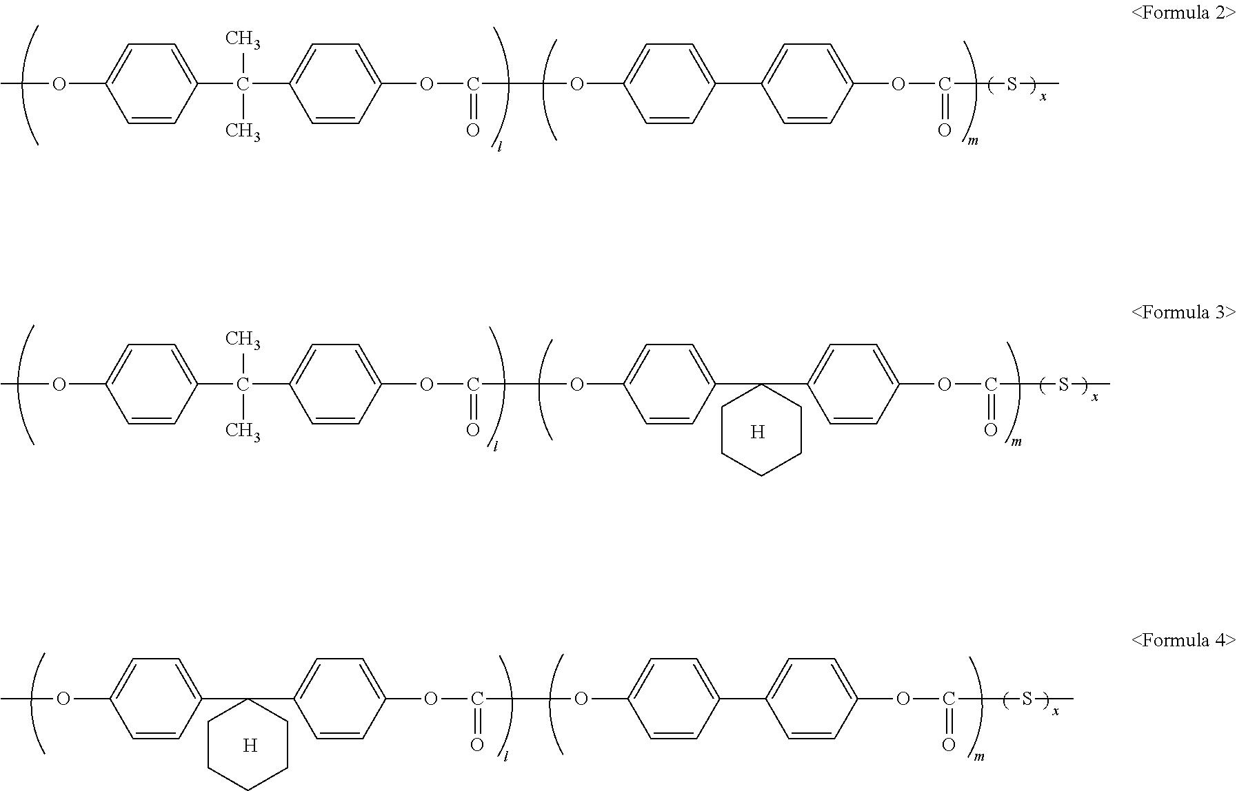
- the first binder resin may be, for example, a binder resin represented by Formula 2 below, a binder resin represented by Formula 3 below, a binder resin represented by Formula 4 below, or a mixture thereof.
- S is the repeating unit represented by Formula 1, and x/(l+m+x) is in a range of about 0.001 to about 0.01.
- x may be, for example, in a range of about 1 to about 50.
- l may be, for example, in a range of about 1 to about 50.
- m may be, for example, in a range of about 1 to about 50.
- the repeating unit S is a silicon-containing functional group and may contribute to a decrease in surface energy. To further decrease a frictional force, x/(l+m+x) may be in a range of about 0.001 to about 0.005.
- a weight average molecular weight of the first binder resin may be in a range of, for example, about 20,000 to about 100,000. When a weight average molecular weight of the first binder resin is too small or too great, the photoreceptor layer may not be formed well.
- the second binder resin is a binder resin that does not contain the repeating unit represented by Formula 1.
- the second binder resin may be, for example, an insulating resin, such as polyvinyl butyral, polyarylate (a condensed polymer of bisphenol A and phthalic acid), polycarbonate, a polyester resin, a phenoxy resin, polyvinyl acetate, an acryl resin, a polyacrylamide resin, polyamide, polyvinyl pyridine, a cellulose-based resin, a urethane resin, an epoxy resin, a silicon resin, polystyrene, polyketone, polyvinyl chloride, a vinyl chloride-a vinyl acid copolymer, polyvinyl acetal, polyacrylonitrile, a phenol resin, a melamine resin, casein, a polyvinyl alcohol, or a polyvinyl pyrrolidone, or an organic photoconductive resin, such as poly N-vinylcarbazole, polyvinyl anth
- a weight ratio of the first binder resin to the second binder resin in the photoreceptor layer may be in a range of about 5:5 to about 9:1.
- the weight ratio of the first binder resin to the second binder resin may be in a range of about 6:4 to about 8:2.
- the photoreceptor layer may have too small a surface frictional force of, for example, less than about 30 gf.
- the photoreceptor layer may have too high a surface frictional force of, for example about, more than 100 gf.
- a solvent that is used in preparing a coating slurry for forming the photoreceptor layer may be any one of various solvents that dissolve the binder resin and do not affect an adjacent layer during coating for forming a photoreceptor layer.
- a possible solvent are methyl isopropyl ketone, methyl isobutyl ketone, 4-methoxy-4-methyl-2-pentanone, isopropyl acetate, tertiary butyl acetate, methyl ethyl ketone, cyclohexanone, 1,2-dichloroethane, 1,1,2-trichloroethane, 1,1,1-trichloroethane, trichloroethylene, tetrachloroethane, dichloromethane, tetrahydrofurane, dioxane, dioxolane, ethyl acetate, and butyl acetate.
- an amount of the solvent may be, for example, in a range of about 500 parts by weight to about 2,000 parts by weight based on 100 parts by weight of a total of the charge-generating material, the charge-transporting material, and the binder resin.
- the coating slurry for forming the photoreceptor layer may be coated on the conductive support.
- the coating method may be soaking coating, ring coating, roll coating, or spray coating.
- the conductive support coated with the coating slurry may be dried at a temperature of about 90 to about 200° C. for about 0.1 to about 2 hours to form a photoreceptor layer
- a thickness of the photoreceptor layer may be in a range of, for example, about 1 to about 50 ⁇ m, about 10 to about 40 ⁇ m, or about 15 to about 40 ⁇ m.
- a thickness of the photoreceptor layer When a thickness of the photoreceptor layer is too small, charges may not be efficiently generated, and when a thickness of the photoreceptor layer is too great, charges may not be moved well and may be trapped, thereby leading to a decrease in image quality.
- a smaller thickness of the photoreceptor layer may lead to a higher image quality.
- a thickness of the photoreceptor layer is too small, due to wear caused by use, a lifespan of the photoreceptor layer may be reduced. A greater thickness of the photoreceptor layer may lead to a longer lifespan of the photoreceptor.
- the thickness of the photoreceptor layer is too great, generated charges are not moved well and are trapped, leading to a decrease in image quality.
- the photoreceptor according to the present embodiment includes: a conductive support; a charge generation layer that is disposed on the conductive support and includes a binder resin and a charge generation material; and a charge transport layer that is disposed on the charge generation layer and includes a binder resin and a charge-transporting material.
- the conductive support is the same as described above.
- the charge generation layer is disposed on the conductive support and includes a binder resin and a charge-generating material.
- the binder resin of the charge generation layer may be, for example, an insulating resin, such as polyvinyl butyral, polyarylate (a condensed polymer of bisphenol A and phthalic acid), polycarbonate, a polyester resin, a phenoxy resin, polyvinyl acetate, an acryl resin, a polyacrylamide resin, polyamide, polyvinyl pyridine, a cellulose-based resin, a urethane resin, an epoxy resin, a silicon resin, polystyrene, polyketone, polyvinyl chloride, a vinyl chloride-a vinylic acid copolymer, polyvinyl acetal, polyacrylonitrile, a phenol resin, a melamine resin, casein, a polyvinyl alcohol, or a polyvinyl pyrrolidone, or an organic photoconductive resin, such as poly N-vinylcarbazole, polyvinyl anthracene, or polyvinylpyrene.
- an organic photoconductive resin
- the charge-generating material is the same as described above.
- An amount of the charge-generating material may be in a range of, for example, about 50 parts by weight to about 300 parts by weight based on 100 parts by weight of the binder resin of the charge generation layer.
- a solvent that is used in preparing a coating slurry for forming the charge generation layer may be any one of various solvents that dissolve the binder resin of the charge generation layer and do not affect an adjacent layer during coating for forming a charge generation layer.
- a possible solvent are methyl isopropyl ketone, methyl isobutyl ketone, 4-methoxy-4-methyl-2-pentanone, isopropyl acetate, tertiary butyl acetate, methyl ethyl ketone, cyclohexanone, 1,2-dichloroethane, 1,1,2-trichloroethane, 1,1,1-trichloroethane, trichloroethylene, tetrachloroethane, dichloromethane, tetrahydrofurane, dioxane, dioxolane, ethyl acetate, and butyl acetate.
- an amount of the solvent may be, for example, in a range of about 500 parts by weight to about 10,000 parts by weigh based on 100 parts by weight of a total of the charge-generating material and the binder resin.
- the coating slurry for forming the charge generation layer may be coated on the conductive support.
- the coating method may be soaking coating, ring coating, roll coating, or spray coating.
- the conductive support coated with the coating slurry may be dried at a temperature of about 90 to about 200° C. for about 0.1 to about 2 hours to form a charge generation layer.
- a thickness of the charge generation layer may be in a range of, for example, about 0.001 to about 10 ⁇ m, about 0.01 to about 10 ⁇ m, or about 0.05 to about 3 ⁇ m.
- a thickness of the charge generation layer is too small, charges may not be efficiently generated, and when a thickness of the charge generation layer is too great, charges may not be moved well and may be trapped, thereby leading to a decrease in image quality.
- the charge transport layer may be disposed on the charge generation layer. Accordingly, the charge transport layer constitutes a surface of the photoreceptor.
- the charge transport layer includes a binder resin and a charge-transporting material.
- the charge-transporting material is the same as described above.
- An amount of the charge-transporting material may be in a range of, for example, about 10 parts by weight to about 100 parts by weight based on 100 parts by weight of the binder resin of the charge transport layer.
- the binder resin of the charge transport layer includes the first binder resin that contains a repeating unit represented by Formula 1 and the second binder resin that does not contain the repeating unit represented by Formula 1.
- the first binder resin is already described above.
- the second binder resin is already described above.
- a weight ratio of the first binder resin to the second binder resin in the charge transport layer may be in a range of about 5:5 to about 9:1.
- the weight ratio of the first binder resin to the second binder resin may be in a range of about 6:4 to about 8:2.
- the photoreceptor may have too small a surface frictional force of, for example, less than about 30 gf.
- the photoreceptor may have too high a surface frictional force of, for example about, more than 100 gf.
- a solvent that is used in preparing a coating slurry for forming the charge transport layer may be any one of various solvents that dissolve the binder resin of the charge transport layer and do not affect an adjacent layer during coating for forming a charge transport layer.
- a possible solvent are methyl isopropyl ketone, methyl isobutyl ketone, 4-methoxy-4-methyl-2-pentanone, isopropyl acetate, tertiary butyl acetate, methyl ethyl ketone, cyclohexanone, 1,2-dichloroethane, 1,1,2-trichloroethane, 1,1,1-trichloroethane, trichloroethylene, tetrachloroethane, dichloromethane, tetrahydrofurane, dioxane, dioxolane, ethyl acetate, and butyl acetate.
- an amount of the solvent may be, for example, in a range of about 500 parts by weight to about 1,000 parts by weight based on 100 parts by weight of a total of the charge-transporting material and the binder resin.
- the coating slurry for forming the charge transport layer may be coated on the charge generation layer.
- the coating method may be soaking coating, ring coating, roll coating, or spray coating.
- the conductive support coated with the coating slurry may be dried at a temperature of about 90 to about 200° C. for about 0.1 to about 2 hours to form a charge transport layer.
- a thickness of the charge transport layer may be in a range of, for example, about 1 to about 50 ⁇ m, about 10 to about 40 ⁇ m, or about 15 to about 40 ⁇ m.
- a thickness of the charge transport layer When a thickness of the charge transport layer is too small, charges may not be efficiently generated, and when a thickness of the charge transport layer is too great, charges may not be moved well and may be trapped, thereby leading to a decrease in image quality. A smaller thickness of the charge transport layer may lead to a higher image quality.
- a thickness of the charge transport layer is too small, due to wear caused by use, a lifespan of the charge transport layer may be reduced. A greater thickness of the charge transport layer may lead to a longer lifespan.
- the thickness of the charge transport layer is too great, generated charges may not be moved well and may be trapped, and thus, image quality may be lowered.
- the photoreceptor according to the present embodiment includes a conductive support; and a charge transport layer that is disposed on the conductive support and includes a binder resin and a charge transporting material; and a charge generation layer that is disposed on the charge transport layer and includes a binder resin and a charge generating material.
- the conductive support is the same as described above.
- the charge transport layer is disposed on the conductive support and includes a binder resin and a charge-transporting material.
- the binder resin of the charge transport layer may be, for example, an insulating resin, such as polyvinyl butyral, polyarylate (a condensed polymer of bisphenol A and phthalic acid), polycarbonate, a polyester resin, a phenoxy resin, polyvinyl acetate, an acryl resin, a polyacrylamide resin, a polyamide, polyvinyl pyridine, a cellulose-based resin, a urethane resin, an epoxy resin, a silicon resin, polystyrene, polyketone, polyvinyl chloride, a vinyl chloride-a vinylic acid copolymer, polyvinyl acetal, polyacrylonitrile, a phenol resin, a melamine resin, casein, a polyvinyl alcohol, or a polyvinyl pyrrolidone, or an organic photoconductive resin, such as poly N-vinylcarbazole, polyvinyl anthracene, or polyvinylpyrene.
- a charge-transporting material is the same as described above.
- An amount of the charge-transporting material may be in a range of, for example, about 10 parts by weight to about 60 parts by weight based on 100 parts by weight of the binder resin of the charge transport layer.
- a solvent that is used in preparing a coating slurry for forming the charge transport layer may be any one of various solvents that dissolve the binder resin of the charge transport layer and do not affect an adjacent layer during coating for forming a charge transport layer.
- a possible solvent are methyl isopropyl ketone, methyl isobutyl ketone, 4-methoxy-4-methyl-2-pentanone, isopropyl acetate, tertiary butyl acetate, methyl ethyl ketone, cyclohexanone, 1,2-dichloroethane, 1,1,2-trichloroethane, 1,1,1-trichloroethane, trichloroethylene, tetrachloroethane, dichloromethane, tetrahydrofurane, dioxane, dioxolane, ethyl acetate, and butyl acetate.
- an amount of the solvent may be, for example, in a range of about 500 parts by weight to about 1,000 parts by weight based on 100 parts by weight of a total of the charge-transporting material and the binder resin.
- the coating slurry for forming the charge transport layer may be coated on the conductive support.
- the coating method may be soaking coating, ring coating, roll coating, or spray coating.
- the conductive support coated with the coating slurry may be dried at a temperature of about 90 to about 200° C. for about 0.1 to about 2 hours to form a charge transport layer.
- a thickness of the charge transport layer may be in a range of, for example, about 1 to about 50 ⁇ m, about 10 to about 40 ⁇ m, or about 15 to about 40 ⁇ m.
- a thickness of the charge transport layer When a thickness of the charge transport layer is too small, charges may not be efficiently generated, and when a thickness of the charge transport layer is too great, charges may not be moved well and may be trapped, thereby leading to a decrease in image quality. A smaller thickness of the charge transport layer may lead to a higher image quality.
- a thickness of the charge transport layer is too small, due to wear caused by use, a lifespan of the charge transport layer may be reduced. A greater thickness of the charge transport layer may lead to a longer lifespan.
- the thickness of the charge transport layer is too great, generated charges may not be moved well and may be trapped, and thus, image quality may be lowered.
- the charge generation layer may be disposed on the charge transport layer. Accordingly, the charge generation layer constitutes a surface of the photoreceptor.
- the charge generation layer includes a binder resin and a charge-generating material.
- the charge-generating material is the same as described above.
- An amount of the charge-generating material may be in a range of, for example, about 50 parts by weight to about 300 parts by weight based on 100 parts by weight of the binder resin of the charge generation layer.
- the binder resin of the charge generation layer includes the first binder resin that contains a repeating unit represented by Formula 1 and the second binder resin that does not contain the repeating unit represented by Formula 1.
- the first binder resin is already described above.
- the second binder resin is already described above.
- a weight ratio of the first binder resin to the second binder resin in the charge generation layer may be in a range of about 5:5 to about 9:1.
- the weight ratio of the first binder resin to the second binder resin may be in a range of about 6:4 to about 8:2.
- the photoreceptor may have too small a surface frictional force of, for example, less than about 30 gf.
- the photoreceptor may have too high a surface frictional force of, for example about, more than 100 gf.
- a solvent that is used in preparing a coating slurry for forming the charge generation layer may be any one of various solvents that dissolve the binder resin of the charge generation layer and do not affect an adjacent layer during coating for forming a charge generation layer.
- a possible solvent are methyl isopropyl ketone, methyl isobutyl ketone, 4-methoxy-4-methyl-2-pentanone, isopropyl acetate, tertiary butyl acetate, methyl ethyl ketone, cyclohexanone, 1,2-dichloroethane, 1,1,2-trichloroethane, 1,1,1-trichloroethane, trichloroethylene, tetrachloroethane, dichloromethane, tetrahydrofurane, dioxane, dioxolane, ethyl acetate, and butyl acetate.
- an amount of the solvent may be, for example, in a range of about 500 parts by weight to about 10,000 parts by weight based on 100 parts by weight of a total of the charge-generating material and the binder resin.
- the coating slurry for forming the charge generation layer may be coated on the charge transport layer.
- the coating method may be soaking coating, ring coating, roll coating, or spray coating.
- the conductive support coated with the coating slurry may be dried at a temperature of about 90 to about 200° C. for about 0.1 to about 2 hours to form a charge generation layer.
- a thickness of the charge generation layer may be in a range of, for example, about 0.001 to about 10 ⁇ m, about 0.01 to about 10 ⁇ m, or about 0.05 to about 3 ⁇ m.
- a thickness of the charge generation layer is too small, charges may not be efficiently generated, and when a thickness of the charge generation layer is too great, charges may not be moved well and may be trapped, thereby leading to a decrease in image quality.
- the surface of the photoreceptor may have a desired level of frictional force.
- a cleaning angle at which slipping between the surface of the photoreceptor surface and a blade is prevented and also, overturning and vibrating of the blade is prevented, may be very easily obtained.
- FIG. 2 is an illustrative view of a device for measuring a surface frictional force.
- a photoreceptor 1 is fixed, and then, 170 g of a weight 3 was attached to a Teflon film 2 (thickness of 0.08 mm, width of 20 mm, and length of 400 mm), and the Teflon film 2 was moved in a movement direction 4 at a movement speed of 108 mm/min by a movement distance of 40 mm.
- a force value shown on a push-pull gauge is defined as a photoreceptor surface frictional force.
- a photoreceptor surface frictional force may be, for example, in a range of about 30 gf to about 100 gf.
- the photoreceptor surface frictional force may be, for example, in a range of about 50 gf to about 80 gf.
- the photoreceptor surface frictional force is too small, at some cleaning angles (for example, from about 6° degrees to about 15 degrees°), slipping may occur between the photoreceptor surface and a blade and thus, the residual ink or toner is not removed.
- slipping occurs between a charging roller and a photoreceptor, and thus, image defects due to defective charging may occur.
- the photoreceptor surface frictional force is too great, a blade may overturn or vibrate very easily. The vibration of the blade causes noise.
- an electro-photographic image forming apparatus includes a photoreceptor and a cleaning blade, wherein the photoreceptor is one of the photoreceptors according to the first to third aspects of the present general inventive concept.
- the photoreceptor is the same as described above.
- a cylindrical photoreceptor 100 contacts a front end of cleaning a blade 200 at a position C.
- the cleaning blade 200 is fixed on a support 300 .
- a dashed line A is an extension line of a straight portion of the cleaning blade 200 .
- a dashed line B contacts the photoreceptor 100 through the position C.
- An angle (that is, a cleaning angle) formed by the cylindrical photoreceptor 100 and the cleaning blade 200 is defined as an angle ( ⁇ ) formed by the dashed line A and a dashed line B.
- the cleaning angle may be in a range of, for example, about 6° to about 15°. In detail, for example, the cleaning angle may be in a range of, for example, about 7° to about 12°. At a greater angle, the residual ink or toner is more easily removed. However, when the angle exceeds a certain range, the blade 200 may overturn, or deform or vibrate, leading to failure in the removal.
- An aluminum drum (a cylindrical drum having a diameter of 24 mm and a length of 248 mm) was used as a conductive support.
- a charge-generating material y-TiOPc, titanyloxy phthalocyanine
- PVB poly(vinyl butyral)
- BX-1 weight average molecular amount of 100,000 to 130,000
- the slurry for forming a charge generation layer was immersion-coated on the drum with an UCL coated thereon, and then dried at a temperature of 120° C. for 20 minutes to form a charge generation layer (thickness: 0.3 ⁇ m).
- a monomer was prepared in an emulsion state by dissolving the monomer in a mixed solution obtained by mixing methylene chloride and a 5 to 10 wt % NaOH aqueous solution (pH 12) at a volumetric ratio of 1:2. Then, triethylamine that was a reaction catalyst was added thereto and the mixture was stirred at a temperature of 30° C. for 12 hours, and then a small amount of phenol was added thereto to stop the reaction.
- the reaction solution was neutralized by using a hydrochloric acid aqueous solution to perform phase-separation, and then a methylene chloride layer was separated therefrom and washed several times with ultrapure water, followed by evaporation, thereby obtaining a binder resin.
- Characteristics of various binder resins obtained from various monomers are as follows:
- a charge-transporting material (a mixture including a charge-transporting material C and a charge-transporting material D at a weight ratio of 1:1) and 50 parts by weight of a second binder resin 1 (PCA) were dissolved in 360 parts by weight of a THF/toluene co-solvent (a weight ratio of 4:1) to prepare a coating composition for forming a charge transport layer.
- a THF/toluene co-solvent a weight ratio of 4:1
- a charge transport layer was formed on the “conductive support including the charge generation layer” obtained according to Preparation Example 1 in the same manner as in Comparative Example 1 except that the second binder resin 2 was used.
- a charge transport layer was formed on “the conductive support including the charge generation layer” obtained according to Preparation Example 1 in the same manner as in Comparative Example 1 except that the second binder resin 3 was used.
- a charge transport layer was formed on “the conductive support including the charge generation layer” obtained according to Preparation Example 1 in the same manner as in Comparative Example 1 except that the second binder resin 4 was used.
- a charge transport layer was formed on “the conductive support including the charge generation layer” obtained according to Preparation Example 1 in the same manner as in Comparative Example 1 except that the second binder resin 5 was used.
- a charge transport layer was formed on “the conductive support including the charge generation layer” obtained according to Preparation Example 1 in the same manner as in Comparative Example 1 except that the second binder resin 6 was used.
- a charge transport layer was formed on “the conductive support including the charge generation layer” obtained according to Preparation Example 1 in the same manner as in Comparative Example 1 except that the second binder resin 7 was used.
- a charge transport layer was formed on “the conductive support including the charge generation layer” obtained according to Preparation Example 1 in the same manner as in Comparative Example 1 except that the second binder resin 8 was used.
- a charge transport layer was formed on “the conductive support including the charge generation layer” obtained according to Preparation Example 1 in the same manner as in Comparative Example 1 except that for use as a binder resin for a charge transport layer, the second binder resin 2 and the first binder resin 9 were used at a weight ratio of 4:6.
- a charge transport layer was formed on “the conductive support including the charge generation layer” obtained according to Preparation Example 1 in the same manner as in Comparative Example 1 except that for use as a binder resin for a charge transport layer, the second binder resin 2 and the first binder resin 11 were used at a weight ratio of 4:6.
- a charge transport layer was formed on “the conductive support including the charge generation layer” obtained according to Preparation Example 1 in the same manner as in Comparative Example 1 except that for use as a binder resin for a charge transport layer, the second binder resin 4 and the first binder resin 9 were used at a weight ratio of 4:6.
- a charge transport layer was formed on “the conductive support including the charge generation layer” obtained according to Preparation Example 1 in the same manner as in Comparative Example 1 except that for use as a binder resin for a charge transport layer, the second binder resin 4 and the first binder resin 11 were used at a weight ratio of 4:6.
- a charge transport layer was formed on “the conductive support including the charge generation layer” obtained according to Preparation Example 1 in the same manner as in Comparative Example 1 except that for use as a binder resin for a charge transport layer, the second binder resin 8 and the first binder resin 9 were used at a weight ratio of 4:6.
- a charge transport layer was formed on “the conductive support including the charge generation layer” obtained according to Preparation Example 1 in the same manner as in Comparative Example 1 except that for use as a binder resin for a charge transport layer, the second binder resin 8 and the first binder resin 11 were used at a weight ratio of 4:6.
- a charge transport layer was formed on “the conductive support including the charge generation layer” obtained according to Preparation Example 1 in the same manner as in Comparative Example 1 except that for use as a binder resin for a charge transport layer, the second binder resin 2 and the first binder resin 9 were used at a weight ratio of 9:1.
- a charge transport layer was formed on “the conductive support including the charge generation layer” obtained according to Preparation Example 1 in the same manner as in Comparative Example 1 except that for use as a binder resin for a charge transport layer, the second binder resin 2 and the first binder resin 9 were used at a weight ratio of 8:2.
- a charge transport layer was formed on “the conductive support including the charge generation layer” obtained according to Preparation Example 1 in the same manner as in Comparative Example 1 except that for use as a binder resin for a charge transport layer, the second binder resin 2 and the first binder resin 9 were used at a weight ratio of 7:3.
- a charge transport layer was formed on “the conductive support including the charge generation layer” obtained according to Preparation Example 1 in the same manner as in Comparative Example 1 except that for use as a binder resin for a charge transport layer, the second binder resin 2 and the first binder resin 9 were used at a weight ratio of 6:4.
- a charge transport layer was formed on “the conductive support including the charge generation layer” obtained according to Preparation Example 1 in the same manner as in Comparative Example 1 except that for use as a binder resin for a charge transport layer, the second binder resin 2 and the first binder resin 9 were used at a weight ratio of 5:5.
- a charge transport layer was formed on “the conductive support including the charge generation layer” obtained according to Preparation Example 1 in the same manner as in Comparative Example 1 except that for use as a binder resin for a charge transport layer, the second binder resin 2 and the first binder resin 11 were used at a weight ratio of 9:1.
- a charge transport layer was formed on “the conductive support including the charge generation layer” obtained according to Preparation Example 1 in the same manner as in Comparative Example 1 except that for use as a binder resin for a charge transport layer, the second binder resin 2 and the first binder resin 11 were used at a weight ratio of 8:2.
- a charge transport layer was formed on “the conductive support including the charge generation layer” obtained according to Preparation Example 1 in the same manner as in Comparative Example 1 except that for use as a binder resin for a charge transport layer, the second binder resin 2 and the first binder resin 11 were used at a weight ratio of 7:3.
- a charge transport layer was formed on “the conductive support including the charge generation layer” obtained according to Preparation Example 1 in the same manner as in Comparative Example 1 except that for use as a binder resin for a charge transport layer, the second binder resin 2 and the first binder resin 11 were used at a weight ratio of 6:4.
- a charge transport layer was formed on “the conductive support including the charge generation layer” obtained according to Preparation Example 1 in the same manner as in Comparative Example 1 except that for use as a binder resin for a charge transport layer, the second binder resin 2 and the first binder resin 11 were used at a weight ratio of 5:5.
- a charge transport layer was formed on “the conductive support including the charge generation layer” obtained according to Preparation Example 1 in the same manner as in Comparative Example 1 except that for use as a binder resin for a charge transport layer, the second binder resin 4 and the first binder resin 9 were used at a weight ratio of 9:1.
- a charge transport layer was formed on “the conductive support including the charge generation layer” obtained according to Preparation Example 1 in the same manner as in Comparative Example 1 except that for use as a binder resin for a charge transport layer, the second binder resin 4 and the first binder resin 9 were used at a weight ratio of 8:2.
- a charge transport layer was formed on “the conductive support including the charge generation layer” obtained according to Preparation Example 1 in the same manner as in Comparative Example 1 except that for use as a binder resin for a charge transport layer, the second binder resin 4 and the first binder resin 9 were used at a weight ratio of 7:3.
- a charge transport layer was formed on “the conductive support including the charge generation layer” obtained according to Preparation Example 1 in the same manner as in Comparative Example 1 except that for use as a binder resin for a charge transport layer, the second binder resin 4 and the first binder resin 9 were used at a weight ratio of 6:4.
- a charge transport layer was formed on “the conductive support including the charge generation layer” obtained according to Preparation Example 1 in the same manner as in Comparative Example 1 except that for use as a binder resin for a charge transport layer, the second binder resin 4 and the first binder resin 9 were used at a weight ratio of 5:5.
- a charge transport layer was formed on “the conductive support including the charge generation layer” obtained according to Preparation Example 1 in the same manner as in Comparative Example 1 except that for use as a binder resin for a charge transport layer, the second binder resin 4 and the first binder resin 11 were used at a weight ratio of 9:1.
- a charge transport layer was formed on “the conductive support including the charge generation layer” obtained according to Preparation Example 1 in the same manner as in Comparative Example 1 except that for use as a binder resin for a charge transport layer, the second binder resin 4 and the first binder resin 11 were used at a weight ratio of 8:2.
- a charge transport layer was formed on “the conductive support including the charge generation layer” obtained according to Preparation Example 1 in the same manner as in Comparative Example 1 except that for use as a binder resin for a charge transport layer, the second binder resin 4 and the first binder resin 11 were used at a weight ratio of 7:3.
- a charge transport layer was formed on “the conductive support including the charge generation layer” obtained according to Preparation Example 1 in the same manner as in Comparative Example 1 except that for use as a binder resin for a charge transport layer, the second binder resin 4 and the first binder resin 11 were used at a weight ratio of 6:4.
- a charge transport layer was formed on “the conductive support including the charge generation layer” obtained according to Preparation Example 1 in the same manner as in Comparative Example 1 except that for use as a binder resin for a charge transport layer, the second binder resin 4 and the first binder resin 11 were used at a weight ratio of 5:5.
- a charge transport layer was formed on “the conductive support including the charge generation layer” obtained according to Preparation Example 1 in the same manner as in Comparative Example 1 except that for use as a binder resin for a charge transport layer, the second binder resin 8 and the first binder resin 9 were used at a weight ratio of 9:1.
- a charge transport layer was formed on “the conductive support including the charge generation layer” obtained according to Preparation Example 1 in the same manner as in Comparative Example 1 except that for use as a binder resin for a charge transport layer, the second binder resin 8 and the first binder resin 9 were used at a weight ratio of 8:2.
- a charge transport layer was formed on “the conductive support including the charge generation layer” obtained according to Preparation Example 1 in the same manner as in Comparative Example 1 except that for use as a binder resin for a charge transport layer, the second binder resin 8 and the first binder resin 9 were used at a weight ratio of 7:3.
- a charge transport layer was formed on “the conductive support including the charge generation layer” obtained according to Preparation Example 1 in the same manner as in Comparative Example 1 except that for use as a binder resin for a charge transport layer, the second binder resin 8 and the first binder resin 9 were used at a weight ratio of 6:4.
- a charge transport layer was formed on “the conductive support including the charge generation layer” obtained according to Preparation Example 1 in the same manner as in Comparative Example 1 except that for use as a binder resin for a charge transport layer, the second binder resin 8 and the first binder resin 9 were used at a weight ratio of 5:5.
- a charge transport layer was formed on “the conductive support including the charge generation layer” obtained according to Preparation Example 1 in the same manner as in Comparative Example 1 except that for use as a binder resin for a charge transport layer, the second binder resin 8 and the first binder resin 11 were used at a weight ratio of 9:1.
- a charge transport layer was formed on “the conductive support including the charge generation layer” obtained according to Preparation Example 1 in the same manner as in Comparative Example 1 except that for use as a binder resin for a charge transport layer, the second binder resin 8 and the first binder resin 11 were used at a weight ratio of 8:2.
- a charge transport layer was formed on “the conductive support including the charge generation layer” obtained according to Preparation Example 1 in the same manner as in Comparative Example 1 except that for use as a binder resin for a charge transport layer, the second binder resin 8 and the first binder resin 11 were used at a weight ratio of 7:3.
- a charge transport layer was formed on “the conductive support including the charge generation layer” obtained according to Preparation Example 1 in the same manner as in Comparative Example 1 except that for use as a binder resin for a charge transport layer, the second binder resin 8 and the first binder resin 11 were used at a weight ratio of 6:4.
- a charge transport layer was formed on “the conductive support including the charge generation layer” obtained according to Preparation Example 1 in the same manner as in Comparative Example 1 except that for use as a binder resin for a charge transport layer, the second binder resin 8 and the first binder resin 11 were used at a weight ratio of 5:5.
- a first binder resin containing a repeating unit represented by Formula 1 reduces a frictional force.
- a frictional force caused by a second binder resin that does not contain the repeating unit represented by Formula 1 may be reduced due to the first binder resin that contains the repeating unit represented by Formula 1.
- the surface of the photoreceptor may have a desired level of frictional force.
Abstract
Description

wherein the respective R are each independently a C1 to C6 alkyl group, a C1 to C6 alkenyl group, a C1 to C6 alkynyl group, or a C6 to 11 aryl group, B is —(CH2)Z—, Z is 2 to 6, and n is 0 to 200.

wherein the respective R are each independently a C1 to C6 alkyl group, a C1 to C6 alkenyl group, a C1 to C6 alkynyl group, or a C6 to 11 aryl group, B is —(CH2)Z—, Z is 2 to 6, and n is 0 to 200.

wherein the respective R are each independently a C1 to C6 alkyl group, a C1 to C6 alkenyl group, a C1 to C6 alkynyl group, or a C6 to 11 aryl group, B is —(CH2)Z—, Z is 2 to 6, and n is 0 to 200.

wherein the respective R are each independently a C1 to C6 alkyl group, alkenyl group, or alkynyl group, or a C6 to C11 aryl group, B is —(CH2)Z—, Z is 2 to 6, and n is 0 to 200.

-
- Monomer used: Bisphenol A (Tokyo Chemical Industry Co., Ltd.)

-
- Weight average molecular weight: 50,000
Second Binder Resin 2 - Monomer used: Bisphenol Z (Tokyo Chemical Industry Co., Ltd.)
- Weight average molecular weight: 50,000

-
- Weight average molecular weight: 48,000
Preparation Example ofSecond Binder Resin 3 - Monomer used: 4,4′-(3,3,5-trimethylcyclohexylidene)bisphenol (Shanghai Chemmole Co., Ltd)
- Weight average molecular weight: 48,000

-
- Weight average molecular weight: 53,000
Preparation Example ofSecond Binder Resin 4
Monomer used: Bisphenol A (Tokyo Chemical Industry Co., Ltd.); 4,4′-Biphenol (Tokyo Chemical Industry Co., Ltd.)
- Weight average molecular weight: 53,000

wherein l:m=85:15
-
- Weight average molecular weight: 51,000
Preparation Example of Second Binder Resin 5 - Monomer used: Bisphenol A (Tokyo Chemical Industry Co., Ltd.); Bisphenol Z (Tokyo Chemical Industry Co., Ltd.)
- Weight average molecular weight: 51,000

wherein l:m=85:15
-
- Weight average molecular weight: 50,000
Preparation Example of Second Binder Resin 6 - Monomer used: Bisphenol A (Tokyo Chemical Industry Co., Ltd.); 4,4′-(3,3,5-trimethylcyclohexylidene)bisphenol (Shanghai Chemmole Co., Ltd.)
- Weight average molecular weight: 50,000

wherein l:m=85:15
-
- Weight average molecular weight: 53,000
Preparation Example of Second Binder Resin 7 - Monomer used: Bisphenol Z (Tokyo Chemical Industry Co., Ltd.); 4,4′-(3,3,5-trimethylcyclohexylidene)bisphenol (Shanghai Chemmole Co., Ltd.)
- Weight average molecular weight: 53,000

wherein l:m=85:15
-
- Weight average molecular weight: 50,000
Preparation Example of Second Binder Resin 8
Monomer used: Bisphenol Z (Tokyo Chemical Industry Co., Ltd.); 4,4′-Biphenol (Tokyo Chemical Industry Co., Ltd.)
- Weight average molecular weight: 50,000

wherein l:m=85:15
-
- Weight average molecular weight: 55,000
Preparation Example of First Binder Resin 9 (Corresponding to Formula 2)
Monomer used: Bisphenol A (Tokyo Chemical Industry Co., Ltd.); 4,4′-Biphenol (Tokyo Chemical Industry Co., Ltd.); Polydialkylsiloxane (see S below)
- Weight average molecular weight: 55,000

-
- wherein l:m:x=85:15:0.015,

R=CH3, B=(CH3)2, n=25
-
- Weight average molecular weight: 52,000
Preparation Example of First Binder Resin 11 (Corresponding to Formula 4)
Monomer used: Bisphenol A (Tokyo Chemical Industry Co., Ltd.); 4,4′-Biphenol (Tokyo Chemical Industry Co., Ltd.); Polydialkylsiloxane (see S below)
- Weight average molecular weight: 52,000

-
- wherein l:m:x=85:15:0.015,

R=CH3, B=(CH3)2, n=25
-
- Weight average molecular weight: 51,000
-
- Charge-transporting material C:

-
- Charge-transporting material D:

| TABLE 1 | ||||
| Measure- | Measure- | Measure- | ||
| ment | ment | ment | ||
| value 1 | value 2 | value 3 | Average | |
| Sample | (gf) | (gf) | (gf) | (gf) |
| Comparative | 135 | 141 | 140 | 139 |
| Example 1 | ||||
| Comparative | 138 | 135 | 140 | 138 |
| Example 2 | ||||
| Comparative | 130 | 132 | 131 | 131 |
| Example 3 | ||||
| Comparative | 120 | 118 | 110 | 116 |
| Example 4 | ||||
| Comparative | 140 | 142 | 141 | 141 |
| Example 5 | ||||
| Comparative | 142 | 145 | 143 | 143 |
| Example 6 | ||||
| Comparative | 136 | 137 | 133 | 135 |
| Example 7 | ||||
| Comparative | 142 | 140 | 145 | 142 |
| Example 8 | ||||
| Comparative | 22 | 24 | 25 | 24 |
| Example 9 | ||||
| Comparative | 24 | 23 | 23 | 23 |
| Example 10 | ||||
| Comparative | 19 | 22 | 22 | 21 |
| Example 11 | ||||
| Comparative | 24 | 25 | 25 | 25 |
| Example 12 | ||||
| Comparative | 23 | 22 | 22 | 22 |
| Example 13 | ||||
| Comparative | 18 | 22 | 25 | 22 |
| Example 14 | ||||
| Example 1 | 104 | 100 | 98 | 101 |
| Example 2 | 82 | 76 | 78 | 79 |
| Example 3 | 72 | 67 | 69 | 69 |
| Example 4 | 52 | 48 | 55 | 52 |
| Example 5 | 35 | 34 | 32 | 34 |
| Example 6 | 100 | 99 | 99 | 99 |
| Example 7 | 80 | 80 | 78 | 79 |
| Example 8 | 66 | 68 | 65 | 66 |
| Example 9 | 50 | 45 | 48 | 48 |
| Example 10 | 30 | 28 | 33 | 30 |
| Example 11 | 103 | 100 | 98 | 100 |
| Example 12 | 83 | 80 | 78 | 80 |
| Example 13 | 70 | 70 | 68 | 69 |
| Example 14 | 50 | 48 | 51 | 50 |
| Example 15 | 33 | 32 | 32 | 32 |
| Example 16 | 98 | 100 | 105 | 101 |
| Example 17 | 85 | 84 | 86 | 85 |
| Example 18 | 65 | 64 | 64 | 64 |
| Example 19 | 48 | 46 | 46 | 47 |
| Example 20 | 32 | 34 | 34 | 33 |
| Example 21 | 96 | 97 | 97 | 97 |
| Example 22 | 82 | 80 | 76 | 79 |
| Example 23 | 66 | 66 | 68 | 67 |
| Example 24 | 54 | 50 | 48 | 51 |
| Example 25 | 30 | 28 | 33 | 30 |
| Example 26 | 98 | 95 | 95 | 96 |
| Example 27 | 80 | 78 | 76 | 78 |
| Example 28 | 68 | 68 | 67 | 68 |
| Example 29 | 50 | 55 | 54 | 53 |
| Example 30 | 30 | 28 | 33 | 30 |
| TABLE 2 | |||
| Cleaning | Blade | Noise caused | Removal of |
| angle (°) | overturning | by vibration | residual toner |
| 6 | not occurred | not occurred | not removed |
| 7 | not occurred | not occurred | not removed |
| 8 | occurred | not occurred | — |
| 9 | occurred | occurred | — |
| 12 | occurred | occurred | — |
| 15 | occurred | occurred | — |
Photoreceptor Surface Frictional Force: 25 gf or Less (Comparative Examples 9 to 14)
| TABLE 3 | |||
| Cleaning | Blade | Noise caused | Removal of |
| angle (° °) | overturning | by vibration | residual toner |
| 6 | not occurred | not occurred | not removed |
| 7 | not occurred | not occurred | not removed |
| 8 | not occurred | not occurred | not removed |
| 9 | not occurred | not occurred | not removed |
| 12 | not occurred | not occurred | not removed |
| 15 | not occurred | not occurred | removed |
Photoreceptor Surface Frictional Force: 30 to 35 gf (Examples 5, 10, 15, 20, 25, and 30)
| TABLE 4 | |||
| Cleaning | Blade | Noise caused | Removal of |
| angle (° °) | overturning | by vibration | residual toner |
| 6 | not occurred | not occurred | Removed (some |
| remained) | |||
| 7 | not occurred | not occurred | removed |
| 8 | not occurred | not occurred | removed |
| 9 | not occurred | not occurred | removed |
| 12 | not occurred | not occurred | removed |
| 15 | not occurred | not occurred | removed |
Photoreceptor Surface Frictional Force: 47 to 69 gf (Examples 3, 4, 8, 9, 13, 14, 18, 19, 23, 24, 28, and 29)
| TABLE 5 | |||
| Cleaning | Blade | Noise caused | Removal of |
| angle (°) | overturning | by vibration | residual toner |
| 6 | not occurred | not occurred | removed |
| 7 | not occurred | not occurred | removed |
| 8 | not occurred | not occurred | removed |
| 9 | not occurred | not occurred | removed |
| 12 | not occurred | not occurred | removed |
| 15 | not occurred | not occurred | removed |
Photoreceptor Surface Frictional Force: 78 to 85 gf (Examples 2, 7, 12, 17, 22, and 27)
| TABLE 6 | |||
| Cleaning | Blade | Noise caused | Removal of |
| angle (°) | overturning | by vibration | residual toner |
| 6 | not occurred | not occurred | removed |
| 7 | not occurred | not occurred | removed |
| 8 | not occurred | not occurred | removed |
| 9 | not occurred | not occurred | removed |
| 12 | not occurred | not occurred | removed |
| 15 | not occurred | not occurred | removed |
Photoreceptor Surface Frictional Force: 96 to 101 gf (Examples 1, 6, 11, 16, 21, and 26)
| TABLE 7 | |||
| Cleaning | Blade | Noise caused | Removal of |
| angle (°) | overturning | by vibration | residual toner |
| 6 | not occurred | not occurred | removed |
| 7 | not occurred | not occurred | removed |
| 8 | not occurred | not occurred | removed |
| 9 | not occurred | not occurred | removed |
| 12 | not occurred | not occurred | removed |
| 15 | occurred | not occurred | — |
Claims (26)


Applications Claiming Priority (2)
| Application Number | Priority Date | Filing Date | Title |
|---|---|---|---|
| KR10-2013-0036440 | 2013-04-03 | ||
| KR20130036440A KR20140120990A (en) | 2013-04-03 | 2013-04-03 | Electro-photographic photoreceptor and image forming apparatus employing the same |
Publications (2)
| Publication Number | Publication Date |
|---|---|
| US20140302431A1 US20140302431A1 (en) | 2014-10-09 |
| US9146457B2 true US9146457B2 (en) | 2015-09-29 |
Family
ID=51654683
Family Applications (1)
| Application Number | Title | Priority Date | Filing Date |
|---|---|---|---|
| US14/043,144 Active 2033-10-21 US9146457B2 (en) | 2013-04-03 | 2013-10-01 | Electro-photographic photoreceptor and image forming apparatus including the same |
Country Status (2)
| Country | Link |
|---|---|
| US (1) | US9146457B2 (en) |
| KR (1) | KR20140120990A (en) |
Citations (10)
| Publication number | Priority date | Publication date | Assignee | Title |
|---|---|---|---|---|
| US3980494A (en) | 1975-01-02 | 1976-09-14 | Beatty Charles L | Method of reducing friction in blade cleaning of imaging surfaces |
| US5162183A (en) | 1990-07-31 | 1992-11-10 | Xerox Corporation | Overcoat for imaging members |
| US5252418A (en) | 1989-08-25 | 1993-10-12 | Hitachi, Ltd. | Electrophotographic photoreceptor with protruding inorganic insulator pieces and an electrophotographic apparatus utilizing the same |
| US6130018A (en) | 1998-07-27 | 2000-10-10 | Kyocera Mita Corporation | Carrier for use in development of electrostatic latent image and image forming apparatus using the carrier |
| US6203962B1 (en) | 1999-06-24 | 2001-03-20 | Konica Corporation | Electrophotographic image forming method, electrophotographic image forming apparatus, and processing cartridge and electrophotographic photoreceptor used therein |
| US20010012594A1 (en) | 1999-12-24 | 2001-08-09 | Ricoh Company Limited | Image bearing material, electrophotographic photoreceptor using the image bearing material, and image forming apparatus using the photoreceptor |
| US20020018948A1 (en) * | 2000-05-25 | 2002-02-14 | Motohiro Takeshima | Electrophotography photosensitive body |
| US20070054207A1 (en) * | 2005-08-23 | 2007-03-08 | Michio Kimura | Electrophotographic photoreceptor, image forming apparatus, and process cartridge |
| US20110014563A1 (en) | 2009-07-20 | 2011-01-20 | Xerox Corporation | Methods of making an improved photoreceptor outer layer |
| US20120201585A1 (en) | 2011-02-03 | 2012-08-09 | Xerox Corporation | Apparatus and methods for delivery of a functional material to an image forming member |
-
2013
- 2013-04-03 KR KR20130036440A patent/KR20140120990A/en not_active Application Discontinuation
- 2013-10-01 US US14/043,144 patent/US9146457B2/en active Active
Patent Citations (11)
| Publication number | Priority date | Publication date | Assignee | Title |
|---|---|---|---|---|
| US3980494A (en) | 1975-01-02 | 1976-09-14 | Beatty Charles L | Method of reducing friction in blade cleaning of imaging surfaces |
| US5252418A (en) | 1989-08-25 | 1993-10-12 | Hitachi, Ltd. | Electrophotographic photoreceptor with protruding inorganic insulator pieces and an electrophotographic apparatus utilizing the same |
| US5162183A (en) | 1990-07-31 | 1992-11-10 | Xerox Corporation | Overcoat for imaging members |
| US6130018A (en) | 1998-07-27 | 2000-10-10 | Kyocera Mita Corporation | Carrier for use in development of electrostatic latent image and image forming apparatus using the carrier |
| US6203962B1 (en) | 1999-06-24 | 2001-03-20 | Konica Corporation | Electrophotographic image forming method, electrophotographic image forming apparatus, and processing cartridge and electrophotographic photoreceptor used therein |
| US20010012594A1 (en) | 1999-12-24 | 2001-08-09 | Ricoh Company Limited | Image bearing material, electrophotographic photoreceptor using the image bearing material, and image forming apparatus using the photoreceptor |
| US6444387B2 (en) | 1999-12-24 | 2002-09-03 | Ricoh Company Limited | Image bearing material, electrophotographic photoreceptor using the image bearing material, and image forming apparatus using the photoreceptor |
| US20020018948A1 (en) * | 2000-05-25 | 2002-02-14 | Motohiro Takeshima | Electrophotography photosensitive body |
| US20070054207A1 (en) * | 2005-08-23 | 2007-03-08 | Michio Kimura | Electrophotographic photoreceptor, image forming apparatus, and process cartridge |
| US20110014563A1 (en) | 2009-07-20 | 2011-01-20 | Xerox Corporation | Methods of making an improved photoreceptor outer layer |
| US20120201585A1 (en) | 2011-02-03 | 2012-08-09 | Xerox Corporation | Apparatus and methods for delivery of a functional material to an image forming member |
Also Published As
| Publication number | Publication date |
|---|---|
| KR20140120990A (en) | 2014-10-15 |
| US20140302431A1 (en) | 2014-10-09 |
Similar Documents
| Publication | Publication Date | Title |
|---|---|---|
| US7901855B2 (en) | Electrophotographic photosensitive member, process cartridge and electrophotographic apparatus | |
| US9766561B2 (en) | Electrophotographic photosensitive member, process cartridge and electrophotographic apparatus | |
| CN111198484B (en) | Electrophotographic photosensitive member, process cartridge, and electrophotographic apparatus | |
| KR20150076085A (en) | Electrophotographic photosensitive member, method of producing electrophotographic photosensitive member, process cartridge, and electrophotographic apparatus | |
| US8512922B2 (en) | Electrophotographic photosensitive member, process cartridge, and electrophotographic apparatus | |
| US10018928B2 (en) | Electrophotographic photosensitive member, method of producing electrophotographic photosensitive member, and process cartridge and electrophotographic apparatus each including the electrophotographic photosensitive member | |
| US9971257B2 (en) | Electrophotographic photosensitive member, process cartridge, and electrophotographic apparatus | |
| US7851113B2 (en) | Electrophotographic photoreceptors having reduced torque and improved mechanical robustness | |
| JP6489824B2 (en) | Electrophotographic photosensitive member, process cartridge, and electrophotographic apparatus | |
| JP6436815B2 (en) | Electrophotographic photosensitive member, process cartridge, and electrophotographic apparatus | |
| US9146457B2 (en) | Electro-photographic photoreceptor and image forming apparatus including the same | |
| JP6370072B2 (en) | Electrophotographic photosensitive member, process cartridge, and electrophotographic apparatus | |
| US10067432B2 (en) | Electrophotographic photosensitive member, process cartridge, and electrophotographic apparatus | |
| JPH08184979A (en) | Electrophotographic photoreceptor and electrophotographic device | |
| US11086241B2 (en) | Electrophotographic photoreceptor, process cartridge, and electrophotographic apparatus | |
| JP2005141027A (en) | Electrophotographic photoreceptor, electrophotographic image forming apparatus and process cartridge | |
| US10649353B2 (en) | Tethered metal dioxide for imaging members | |
| JP2010066673A (en) | Method for manufacturing multilayer electrophotographic photoreceptor | |
| JP3779210B2 (en) | Electrophotographic photoreceptor and method for producing the photoreceptor | |
| JP2005157291A (en) | Layered type electrophotographic photoreceptor and image forming apparatus | |
| JP2887558B2 (en) | Electrophotographic photoreceptor | |
| JP6622553B2 (en) | Electrophotographic photosensitive member, process cartridge, and electrophotographic apparatus | |
| JPH11174705A (en) | Electrophotographic photoreceptor containing electron transferring material in undercoat layer | |
| JPH0531136B2 (en) | ||
| JPH05224452A (en) | Electrophotographic sensitive body |
Legal Events
| Date | Code | Title | Description |
|---|---|---|---|
| AS | Assignment |
Owner name: SAMSUNG ELECTRONICS CO., LTD., KOREA, REPUBLIC OF Free format text: ASSIGNMENT OF ASSIGNORS INTEREST;ASSIGNORS:KIM, SEUNG-JU;KIM, JI-UK;REEL/FRAME:031434/0981 Effective date: 20130913 |
|
| FEPP | Fee payment procedure |
Free format text: PAYOR NUMBER ASSIGNED (ORIGINAL EVENT CODE: ASPN); ENTITY STATUS OF PATENT OWNER: LARGE ENTITY |
|
| STCF | Information on status: patent grant |
Free format text: PATENTED CASE |
|
| AS | Assignment |
Owner name: S-PRINTING SOLUTION CO., LTD., KOREA, REPUBLIC OF Free format text: ASSIGNMENT OF ASSIGNORS INTEREST;ASSIGNOR:SAMSUNG ELECTRONICS CO., LTD;REEL/FRAME:041852/0125 Effective date: 20161104 |
|
| AS | Assignment |
Owner name: HP PRINTING KOREA CO., LTD., KOREA, REPUBLIC OF Free format text: CHANGE OF NAME;ASSIGNOR:S-PRINTING SOLUTION CO., LTD.;REEL/FRAME:047370/0405 Effective date: 20180316 |
|
| AS | Assignment |
Owner name: HP PRINTING KOREA CO., LTD., KOREA, REPUBLIC OF Free format text: CORRECTIVE ASSIGNMENT TO CORRECT THE DOCUMENTATION EVIDENCING THE CHANGE OF NAME PREVIOUSLY RECORDED ON REEL 047370 FRAME 0405. ASSIGNOR(S) HEREBY CONFIRMS THE CHANGE OF NAME;ASSIGNOR:S-PRINTING SOLUTION CO., LTD.;REEL/FRAME:047769/0001 Effective date: 20180316 |
|
| MAFP | Maintenance fee payment |
Free format text: PAYMENT OF MAINTENANCE FEE, 4TH YEAR, LARGE ENTITY (ORIGINAL EVENT CODE: M1551); ENTITY STATUS OF PATENT OWNER: LARGE ENTITY Year of fee payment: 4 |
|
| AS | Assignment |
Owner name: HP PRINTING KOREA CO., LTD., KOREA, REPUBLIC OF Free format text: CHANGE OF LEGAL ENTITY EFFECTIVE AUG. 31, 2018;ASSIGNOR:HP PRINTING KOREA CO., LTD.;REEL/FRAME:050938/0139 Effective date: 20190611 |
|
| AS | Assignment |
Owner name: HEWLETT-PACKARD DEVELOPMENT COMPANY, L.P., TEXAS Free format text: CONFIRMATORY ASSIGNMENT EFFECTIVE NOVEMBER 1, 2018;ASSIGNOR:HP PRINTING KOREA CO., LTD.;REEL/FRAME:050747/0080 Effective date: 20190826 |
|
| MAFP | Maintenance fee payment |
Free format text: PAYMENT OF MAINTENANCE FEE, 8TH YEAR, LARGE ENTITY (ORIGINAL EVENT CODE: M1552); ENTITY STATUS OF PATENT OWNER: LARGE ENTITY Year of fee payment: 8 |