US9142522B2 - Semiconductor device and method of forming RDL under bump for electrical connection to enclosed bump - Google Patents
Semiconductor device and method of forming RDL under bump for electrical connection to enclosed bump Download PDFInfo
- Publication number
- US9142522B2 US9142522B2 US13/307,849 US201113307849A US9142522B2 US 9142522 B2 US9142522 B2 US 9142522B2 US 201113307849 A US201113307849 A US 201113307849A US 9142522 B2 US9142522 B2 US 9142522B2
- Authority
- US
- United States
- Prior art keywords
- conductive layer
- insulating layer
- layer
- semiconductor
- over
- Prior art date
- Legal status (The legal status is an assumption and is not a legal conclusion. Google has not performed a legal analysis and makes no representation as to the accuracy of the status listed.)
- Active, expires
Links
Images


Classifications
-
- H—ELECTRICITY
- H01—ELECTRIC ELEMENTS
- H01L—SEMICONDUCTOR DEVICES NOT COVERED BY CLASS H10
- H01L24/00—Arrangements for connecting or disconnecting semiconductor or solid-state bodies; Methods or apparatus related thereto
- H01L24/01—Means for bonding being attached to, or being formed on, the surface to be connected, e.g. chip-to-package, die-attach, "first-level" interconnects; Manufacturing methods related thereto
- H01L24/10—Bump connectors ; Manufacturing methods related thereto
- H01L24/12—Structure, shape, material or disposition of the bump connectors prior to the connecting process
- H01L24/14—Structure, shape, material or disposition of the bump connectors prior to the connecting process of a plurality of bump connectors
-
- H—ELECTRICITY
- H01—ELECTRIC ELEMENTS
- H01L—SEMICONDUCTOR DEVICES NOT COVERED BY CLASS H10
- H01L24/00—Arrangements for connecting or disconnecting semiconductor or solid-state bodies; Methods or apparatus related thereto
- H01L24/01—Means for bonding being attached to, or being formed on, the surface to be connected, e.g. chip-to-package, die-attach, "first-level" interconnects; Manufacturing methods related thereto
- H01L24/02—Bonding areas ; Manufacturing methods related thereto
- H01L24/04—Structure, shape, material or disposition of the bonding areas prior to the connecting process
- H01L24/05—Structure, shape, material or disposition of the bonding areas prior to the connecting process of an individual bonding area
-
- H—ELECTRICITY
- H01—ELECTRIC ELEMENTS
- H01L—SEMICONDUCTOR DEVICES NOT COVERED BY CLASS H10
- H01L2224/00—Indexing scheme for arrangements for connecting or disconnecting semiconductor or solid-state bodies and methods related thereto as covered by H01L24/00
- H01L2224/01—Means for bonding being attached to, or being formed on, the surface to be connected, e.g. chip-to-package, die-attach, "first-level" interconnects; Manufacturing methods related thereto
- H01L2224/02—Bonding areas; Manufacturing methods related thereto
- H01L2224/0212—Auxiliary members for bonding areas, e.g. spacers
- H01L2224/02122—Auxiliary members for bonding areas, e.g. spacers being formed on the semiconductor or solid-state body
- H01L2224/02123—Auxiliary members for bonding areas, e.g. spacers being formed on the semiconductor or solid-state body inside the bonding area
- H01L2224/02125—Reinforcing structures
-
- H—ELECTRICITY
- H01—ELECTRIC ELEMENTS
- H01L—SEMICONDUCTOR DEVICES NOT COVERED BY CLASS H10
- H01L2224/00—Indexing scheme for arrangements for connecting or disconnecting semiconductor or solid-state bodies and methods related thereto as covered by H01L24/00
- H01L2224/01—Means for bonding being attached to, or being formed on, the surface to be connected, e.g. chip-to-package, die-attach, "first-level" interconnects; Manufacturing methods related thereto
- H01L2224/02—Bonding areas; Manufacturing methods related thereto
- H01L2224/023—Redistribution layers [RDL] for bonding areas
- H01L2224/0231—Manufacturing methods of the redistribution layers
- H01L2224/02311—Additive methods
-
- H—ELECTRICITY
- H01—ELECTRIC ELEMENTS
- H01L—SEMICONDUCTOR DEVICES NOT COVERED BY CLASS H10
- H01L2224/00—Indexing scheme for arrangements for connecting or disconnecting semiconductor or solid-state bodies and methods related thereto as covered by H01L24/00
- H01L2224/01—Means for bonding being attached to, or being formed on, the surface to be connected, e.g. chip-to-package, die-attach, "first-level" interconnects; Manufacturing methods related thereto
- H01L2224/02—Bonding areas; Manufacturing methods related thereto
- H01L2224/023—Redistribution layers [RDL] for bonding areas
- H01L2224/0231—Manufacturing methods of the redistribution layers
- H01L2224/02313—Subtractive methods
-
- H—ELECTRICITY
- H01—ELECTRIC ELEMENTS
- H01L—SEMICONDUCTOR DEVICES NOT COVERED BY CLASS H10
- H01L2224/00—Indexing scheme for arrangements for connecting or disconnecting semiconductor or solid-state bodies and methods related thereto as covered by H01L24/00
- H01L2224/01—Means for bonding being attached to, or being formed on, the surface to be connected, e.g. chip-to-package, die-attach, "first-level" interconnects; Manufacturing methods related thereto
- H01L2224/02—Bonding areas; Manufacturing methods related thereto
- H01L2224/023—Redistribution layers [RDL] for bonding areas
- H01L2224/0233—Structure of the redistribution layers
- H01L2224/02331—Multilayer structure
-
- H—ELECTRICITY
- H01—ELECTRIC ELEMENTS
- H01L—SEMICONDUCTOR DEVICES NOT COVERED BY CLASS H10
- H01L2224/00—Indexing scheme for arrangements for connecting or disconnecting semiconductor or solid-state bodies and methods related thereto as covered by H01L24/00
- H01L2224/01—Means for bonding being attached to, or being formed on, the surface to be connected, e.g. chip-to-package, die-attach, "first-level" interconnects; Manufacturing methods related thereto
- H01L2224/02—Bonding areas; Manufacturing methods related thereto
- H01L2224/023—Redistribution layers [RDL] for bonding areas
- H01L2224/0237—Disposition of the redistribution layers
- H01L2224/02375—Top view
-
- H—ELECTRICITY
- H01—ELECTRIC ELEMENTS
- H01L—SEMICONDUCTOR DEVICES NOT COVERED BY CLASS H10
- H01L2224/00—Indexing scheme for arrangements for connecting or disconnecting semiconductor or solid-state bodies and methods related thereto as covered by H01L24/00
- H01L2224/01—Means for bonding being attached to, or being formed on, the surface to be connected, e.g. chip-to-package, die-attach, "first-level" interconnects; Manufacturing methods related thereto
- H01L2224/02—Bonding areas; Manufacturing methods related thereto
- H01L2224/023—Redistribution layers [RDL] for bonding areas
- H01L2224/0237—Disposition of the redistribution layers
- H01L2224/02377—Fan-in arrangement
-
- H—ELECTRICITY
- H01—ELECTRIC ELEMENTS
- H01L—SEMICONDUCTOR DEVICES NOT COVERED BY CLASS H10
- H01L2224/00—Indexing scheme for arrangements for connecting or disconnecting semiconductor or solid-state bodies and methods related thereto as covered by H01L24/00
- H01L2224/01—Means for bonding being attached to, or being formed on, the surface to be connected, e.g. chip-to-package, die-attach, "first-level" interconnects; Manufacturing methods related thereto
- H01L2224/02—Bonding areas; Manufacturing methods related thereto
- H01L2224/023—Redistribution layers [RDL] for bonding areas
- H01L2224/0237—Disposition of the redistribution layers
- H01L2224/02381—Side view
-
- H—ELECTRICITY
- H01—ELECTRIC ELEMENTS
- H01L—SEMICONDUCTOR DEVICES NOT COVERED BY CLASS H10
- H01L2224/00—Indexing scheme for arrangements for connecting or disconnecting semiconductor or solid-state bodies and methods related thereto as covered by H01L24/00
- H01L2224/01—Means for bonding being attached to, or being formed on, the surface to be connected, e.g. chip-to-package, die-attach, "first-level" interconnects; Manufacturing methods related thereto
- H01L2224/02—Bonding areas; Manufacturing methods related thereto
- H01L2224/023—Redistribution layers [RDL] for bonding areas
- H01L2224/0239—Material of the redistribution layers
-
- H—ELECTRICITY
- H01—ELECTRIC ELEMENTS
- H01L—SEMICONDUCTOR DEVICES NOT COVERED BY CLASS H10
- H01L2224/00—Indexing scheme for arrangements for connecting or disconnecting semiconductor or solid-state bodies and methods related thereto as covered by H01L24/00
- H01L2224/01—Means for bonding being attached to, or being formed on, the surface to be connected, e.g. chip-to-package, die-attach, "first-level" interconnects; Manufacturing methods related thereto
- H01L2224/02—Bonding areas; Manufacturing methods related thereto
- H01L2224/04—Structure, shape, material or disposition of the bonding areas prior to the connecting process
- H01L2224/0401—Bonding areas specifically adapted for bump connectors, e.g. under bump metallisation [UBM]
-
- H—ELECTRICITY
- H01—ELECTRIC ELEMENTS
- H01L—SEMICONDUCTOR DEVICES NOT COVERED BY CLASS H10
- H01L2224/00—Indexing scheme for arrangements for connecting or disconnecting semiconductor or solid-state bodies and methods related thereto as covered by H01L24/00
- H01L2224/01—Means for bonding being attached to, or being formed on, the surface to be connected, e.g. chip-to-package, die-attach, "first-level" interconnects; Manufacturing methods related thereto
- H01L2224/02—Bonding areas; Manufacturing methods related thereto
- H01L2224/04—Structure, shape, material or disposition of the bonding areas prior to the connecting process
- H01L2224/05—Structure, shape, material or disposition of the bonding areas prior to the connecting process of an individual bonding area
- H01L2224/05001—Internal layers
- H01L2224/0501—Shape
- H01L2224/05016—Shape in side view
- H01L2224/05018—Shape in side view being a conformal layer on a patterned surface
-
- H—ELECTRICITY
- H01—ELECTRIC ELEMENTS
- H01L—SEMICONDUCTOR DEVICES NOT COVERED BY CLASS H10
- H01L2224/00—Indexing scheme for arrangements for connecting or disconnecting semiconductor or solid-state bodies and methods related thereto as covered by H01L24/00
- H01L2224/01—Means for bonding being attached to, or being formed on, the surface to be connected, e.g. chip-to-package, die-attach, "first-level" interconnects; Manufacturing methods related thereto
- H01L2224/02—Bonding areas; Manufacturing methods related thereto
- H01L2224/04—Structure, shape, material or disposition of the bonding areas prior to the connecting process
- H01L2224/05—Structure, shape, material or disposition of the bonding areas prior to the connecting process of an individual bonding area
- H01L2224/05001—Internal layers
- H01L2224/0502—Disposition
- H01L2224/05022—Disposition the internal layer being at least partially embedded in the surface
-
- H—ELECTRICITY
- H01—ELECTRIC ELEMENTS
- H01L—SEMICONDUCTOR DEVICES NOT COVERED BY CLASS H10
- H01L2224/00—Indexing scheme for arrangements for connecting or disconnecting semiconductor or solid-state bodies and methods related thereto as covered by H01L24/00
- H01L2224/01—Means for bonding being attached to, or being formed on, the surface to be connected, e.g. chip-to-package, die-attach, "first-level" interconnects; Manufacturing methods related thereto
- H01L2224/02—Bonding areas; Manufacturing methods related thereto
- H01L2224/04—Structure, shape, material or disposition of the bonding areas prior to the connecting process
- H01L2224/05—Structure, shape, material or disposition of the bonding areas prior to the connecting process of an individual bonding area
- H01L2224/05001—Internal layers
- H01L2224/0502—Disposition
- H01L2224/05024—Disposition the internal layer being disposed on a redistribution layer on the semiconductor or solid-state body
-
- H—ELECTRICITY
- H01—ELECTRIC ELEMENTS
- H01L—SEMICONDUCTOR DEVICES NOT COVERED BY CLASS H10
- H01L2224/00—Indexing scheme for arrangements for connecting or disconnecting semiconductor or solid-state bodies and methods related thereto as covered by H01L24/00
- H01L2224/01—Means for bonding being attached to, or being formed on, the surface to be connected, e.g. chip-to-package, die-attach, "first-level" interconnects; Manufacturing methods related thereto
- H01L2224/02—Bonding areas; Manufacturing methods related thereto
- H01L2224/04—Structure, shape, material or disposition of the bonding areas prior to the connecting process
- H01L2224/05—Structure, shape, material or disposition of the bonding areas prior to the connecting process of an individual bonding area
- H01L2224/05001—Internal layers
- H01L2224/05075—Plural internal layers
- H01L2224/0508—Plural internal layers being stacked
- H01L2224/05082—Two-layer arrangements
-
- H—ELECTRICITY
- H01—ELECTRIC ELEMENTS
- H01L—SEMICONDUCTOR DEVICES NOT COVERED BY CLASS H10
- H01L2224/00—Indexing scheme for arrangements for connecting or disconnecting semiconductor or solid-state bodies and methods related thereto as covered by H01L24/00
- H01L2224/01—Means for bonding being attached to, or being formed on, the surface to be connected, e.g. chip-to-package, die-attach, "first-level" interconnects; Manufacturing methods related thereto
- H01L2224/02—Bonding areas; Manufacturing methods related thereto
- H01L2224/04—Structure, shape, material or disposition of the bonding areas prior to the connecting process
- H01L2224/05—Structure, shape, material or disposition of the bonding areas prior to the connecting process of an individual bonding area
- H01L2224/05001—Internal layers
- H01L2224/05099—Material
- H01L2224/051—Material with a principal constituent of the material being a metal or a metalloid, e.g. boron [B], silicon [Si], germanium [Ge], arsenic [As], antimony [Sb], tellurium [Te] and polonium [Po], and alloys thereof
- H01L2224/05138—Material with a principal constituent of the material being a metal or a metalloid, e.g. boron [B], silicon [Si], germanium [Ge], arsenic [As], antimony [Sb], tellurium [Te] and polonium [Po], and alloys thereof the principal constituent melting at a temperature of greater than or equal to 950°C and less than 1550°C
- H01L2224/05155—Nickel [Ni] as principal constituent
-
- H—ELECTRICITY
- H01—ELECTRIC ELEMENTS
- H01L—SEMICONDUCTOR DEVICES NOT COVERED BY CLASS H10
- H01L2224/00—Indexing scheme for arrangements for connecting or disconnecting semiconductor or solid-state bodies and methods related thereto as covered by H01L24/00
- H01L2224/01—Means for bonding being attached to, or being formed on, the surface to be connected, e.g. chip-to-package, die-attach, "first-level" interconnects; Manufacturing methods related thereto
- H01L2224/02—Bonding areas; Manufacturing methods related thereto
- H01L2224/04—Structure, shape, material or disposition of the bonding areas prior to the connecting process
- H01L2224/05—Structure, shape, material or disposition of the bonding areas prior to the connecting process of an individual bonding area
- H01L2224/05001—Internal layers
- H01L2224/05099—Material
- H01L2224/051—Material with a principal constituent of the material being a metal or a metalloid, e.g. boron [B], silicon [Si], germanium [Ge], arsenic [As], antimony [Sb], tellurium [Te] and polonium [Po], and alloys thereof
- H01L2224/05163—Material with a principal constituent of the material being a metal or a metalloid, e.g. boron [B], silicon [Si], germanium [Ge], arsenic [As], antimony [Sb], tellurium [Te] and polonium [Po], and alloys thereof the principal constituent melting at a temperature of greater than 1550°C
- H01L2224/05164—Palladium [Pd] as principal constituent
-
- H—ELECTRICITY
- H01—ELECTRIC ELEMENTS
- H01L—SEMICONDUCTOR DEVICES NOT COVERED BY CLASS H10
- H01L2224/00—Indexing scheme for arrangements for connecting or disconnecting semiconductor or solid-state bodies and methods related thereto as covered by H01L24/00
- H01L2224/01—Means for bonding being attached to, or being formed on, the surface to be connected, e.g. chip-to-package, die-attach, "first-level" interconnects; Manufacturing methods related thereto
- H01L2224/02—Bonding areas; Manufacturing methods related thereto
- H01L2224/04—Structure, shape, material or disposition of the bonding areas prior to the connecting process
- H01L2224/05—Structure, shape, material or disposition of the bonding areas prior to the connecting process of an individual bonding area
- H01L2224/05001—Internal layers
- H01L2224/05099—Material
- H01L2224/051—Material with a principal constituent of the material being a metal or a metalloid, e.g. boron [B], silicon [Si], germanium [Ge], arsenic [As], antimony [Sb], tellurium [Te] and polonium [Po], and alloys thereof
- H01L2224/05163—Material with a principal constituent of the material being a metal or a metalloid, e.g. boron [B], silicon [Si], germanium [Ge], arsenic [As], antimony [Sb], tellurium [Te] and polonium [Po], and alloys thereof the principal constituent melting at a temperature of greater than 1550°C
- H01L2224/05166—Titanium [Ti] as principal constituent
-
- H—ELECTRICITY
- H01—ELECTRIC ELEMENTS
- H01L—SEMICONDUCTOR DEVICES NOT COVERED BY CLASS H10
- H01L2224/00—Indexing scheme for arrangements for connecting or disconnecting semiconductor or solid-state bodies and methods related thereto as covered by H01L24/00
- H01L2224/01—Means for bonding being attached to, or being formed on, the surface to be connected, e.g. chip-to-package, die-attach, "first-level" interconnects; Manufacturing methods related thereto
- H01L2224/02—Bonding areas; Manufacturing methods related thereto
- H01L2224/04—Structure, shape, material or disposition of the bonding areas prior to the connecting process
- H01L2224/05—Structure, shape, material or disposition of the bonding areas prior to the connecting process of an individual bonding area
- H01L2224/05001—Internal layers
- H01L2224/05099—Material
- H01L2224/051—Material with a principal constituent of the material being a metal or a metalloid, e.g. boron [B], silicon [Si], germanium [Ge], arsenic [As], antimony [Sb], tellurium [Te] and polonium [Po], and alloys thereof
- H01L2224/05163—Material with a principal constituent of the material being a metal or a metalloid, e.g. boron [B], silicon [Si], germanium [Ge], arsenic [As], antimony [Sb], tellurium [Te] and polonium [Po], and alloys thereof the principal constituent melting at a temperature of greater than 1550°C
- H01L2224/05169—Platinum [Pt] as principal constituent
-
- H—ELECTRICITY
- H01—ELECTRIC ELEMENTS
- H01L—SEMICONDUCTOR DEVICES NOT COVERED BY CLASS H10
- H01L2224/00—Indexing scheme for arrangements for connecting or disconnecting semiconductor or solid-state bodies and methods related thereto as covered by H01L24/00
- H01L2224/01—Means for bonding being attached to, or being formed on, the surface to be connected, e.g. chip-to-package, die-attach, "first-level" interconnects; Manufacturing methods related thereto
- H01L2224/02—Bonding areas; Manufacturing methods related thereto
- H01L2224/04—Structure, shape, material or disposition of the bonding areas prior to the connecting process
- H01L2224/05—Structure, shape, material or disposition of the bonding areas prior to the connecting process of an individual bonding area
- H01L2224/05001—Internal layers
- H01L2224/05099—Material
- H01L2224/051—Material with a principal constituent of the material being a metal or a metalloid, e.g. boron [B], silicon [Si], germanium [Ge], arsenic [As], antimony [Sb], tellurium [Te] and polonium [Po], and alloys thereof
- H01L2224/05163—Material with a principal constituent of the material being a metal or a metalloid, e.g. boron [B], silicon [Si], germanium [Ge], arsenic [As], antimony [Sb], tellurium [Te] and polonium [Po], and alloys thereof the principal constituent melting at a temperature of greater than 1550°C
- H01L2224/05171—Chromium [Cr] as principal constituent
-
- H—ELECTRICITY
- H01—ELECTRIC ELEMENTS
- H01L—SEMICONDUCTOR DEVICES NOT COVERED BY CLASS H10
- H01L2224/00—Indexing scheme for arrangements for connecting or disconnecting semiconductor or solid-state bodies and methods related thereto as covered by H01L24/00
- H01L2224/01—Means for bonding being attached to, or being formed on, the surface to be connected, e.g. chip-to-package, die-attach, "first-level" interconnects; Manufacturing methods related thereto
- H01L2224/02—Bonding areas; Manufacturing methods related thereto
- H01L2224/04—Structure, shape, material or disposition of the bonding areas prior to the connecting process
- H01L2224/05—Structure, shape, material or disposition of the bonding areas prior to the connecting process of an individual bonding area
- H01L2224/05001—Internal layers
- H01L2224/05099—Material
- H01L2224/051—Material with a principal constituent of the material being a metal or a metalloid, e.g. boron [B], silicon [Si], germanium [Ge], arsenic [As], antimony [Sb], tellurium [Te] and polonium [Po], and alloys thereof
- H01L2224/05163—Material with a principal constituent of the material being a metal or a metalloid, e.g. boron [B], silicon [Si], germanium [Ge], arsenic [As], antimony [Sb], tellurium [Te] and polonium [Po], and alloys thereof the principal constituent melting at a temperature of greater than 1550°C
- H01L2224/05173—Rhodium [Rh] as principal constituent
-
- H—ELECTRICITY
- H01—ELECTRIC ELEMENTS
- H01L—SEMICONDUCTOR DEVICES NOT COVERED BY CLASS H10
- H01L2224/00—Indexing scheme for arrangements for connecting or disconnecting semiconductor or solid-state bodies and methods related thereto as covered by H01L24/00
- H01L2224/01—Means for bonding being attached to, or being formed on, the surface to be connected, e.g. chip-to-package, die-attach, "first-level" interconnects; Manufacturing methods related thereto
- H01L2224/02—Bonding areas; Manufacturing methods related thereto
- H01L2224/04—Structure, shape, material or disposition of the bonding areas prior to the connecting process
- H01L2224/05—Structure, shape, material or disposition of the bonding areas prior to the connecting process of an individual bonding area
- H01L2224/05001—Internal layers
- H01L2224/05099—Material
- H01L2224/05186—Material with a principal constituent of the material being a non metallic, non metalloid inorganic material
- H01L2224/05187—Ceramics, e.g. crystalline carbides, nitrides or oxides
-
- H—ELECTRICITY
- H01—ELECTRIC ELEMENTS
- H01L—SEMICONDUCTOR DEVICES NOT COVERED BY CLASS H10
- H01L2224/00—Indexing scheme for arrangements for connecting or disconnecting semiconductor or solid-state bodies and methods related thereto as covered by H01L24/00
- H01L2224/01—Means for bonding being attached to, or being formed on, the surface to be connected, e.g. chip-to-package, die-attach, "first-level" interconnects; Manufacturing methods related thereto
- H01L2224/02—Bonding areas; Manufacturing methods related thereto
- H01L2224/04—Structure, shape, material or disposition of the bonding areas prior to the connecting process
- H01L2224/05—Structure, shape, material or disposition of the bonding areas prior to the connecting process of an individual bonding area
- H01L2224/0554—External layer
- H01L2224/0555—Shape
- H01L2224/05552—Shape in top view
-
- H—ELECTRICITY
- H01—ELECTRIC ELEMENTS
- H01L—SEMICONDUCTOR DEVICES NOT COVERED BY CLASS H10
- H01L2224/00—Indexing scheme for arrangements for connecting or disconnecting semiconductor or solid-state bodies and methods related thereto as covered by H01L24/00
- H01L2224/01—Means for bonding being attached to, or being formed on, the surface to be connected, e.g. chip-to-package, die-attach, "first-level" interconnects; Manufacturing methods related thereto
- H01L2224/02—Bonding areas; Manufacturing methods related thereto
- H01L2224/04—Structure, shape, material or disposition of the bonding areas prior to the connecting process
- H01L2224/05—Structure, shape, material or disposition of the bonding areas prior to the connecting process of an individual bonding area
- H01L2224/0554—External layer
- H01L2224/0555—Shape
- H01L2224/05556—Shape in side view
- H01L2224/05558—Shape in side view conformal layer on a patterned surface
-
- H—ELECTRICITY
- H01—ELECTRIC ELEMENTS
- H01L—SEMICONDUCTOR DEVICES NOT COVERED BY CLASS H10
- H01L2224/00—Indexing scheme for arrangements for connecting or disconnecting semiconductor or solid-state bodies and methods related thereto as covered by H01L24/00
- H01L2224/01—Means for bonding being attached to, or being formed on, the surface to be connected, e.g. chip-to-package, die-attach, "first-level" interconnects; Manufacturing methods related thereto
- H01L2224/02—Bonding areas; Manufacturing methods related thereto
- H01L2224/04—Structure, shape, material or disposition of the bonding areas prior to the connecting process
- H01L2224/05—Structure, shape, material or disposition of the bonding areas prior to the connecting process of an individual bonding area
- H01L2224/0554—External layer
- H01L2224/0556—Disposition
- H01L2224/05567—Disposition the external layer being at least partially embedded in the surface
-
- H—ELECTRICITY
- H01—ELECTRIC ELEMENTS
- H01L—SEMICONDUCTOR DEVICES NOT COVERED BY CLASS H10
- H01L2224/00—Indexing scheme for arrangements for connecting or disconnecting semiconductor or solid-state bodies and methods related thereto as covered by H01L24/00
- H01L2224/01—Means for bonding being attached to, or being formed on, the surface to be connected, e.g. chip-to-package, die-attach, "first-level" interconnects; Manufacturing methods related thereto
- H01L2224/02—Bonding areas; Manufacturing methods related thereto
- H01L2224/04—Structure, shape, material or disposition of the bonding areas prior to the connecting process
- H01L2224/05—Structure, shape, material or disposition of the bonding areas prior to the connecting process of an individual bonding area
- H01L2224/0554—External layer
- H01L2224/0556—Disposition
- H01L2224/05569—Disposition the external layer being disposed on a redistribution layer on the semiconductor or solid-state body
-
- H—ELECTRICITY
- H01—ELECTRIC ELEMENTS
- H01L—SEMICONDUCTOR DEVICES NOT COVERED BY CLASS H10
- H01L2224/00—Indexing scheme for arrangements for connecting or disconnecting semiconductor or solid-state bodies and methods related thereto as covered by H01L24/00
- H01L2224/01—Means for bonding being attached to, or being formed on, the surface to be connected, e.g. chip-to-package, die-attach, "first-level" interconnects; Manufacturing methods related thereto
- H01L2224/02—Bonding areas; Manufacturing methods related thereto
- H01L2224/04—Structure, shape, material or disposition of the bonding areas prior to the connecting process
- H01L2224/05—Structure, shape, material or disposition of the bonding areas prior to the connecting process of an individual bonding area
- H01L2224/0554—External layer
- H01L2224/05575—Plural external layers
- H01L2224/0558—Plural external layers being stacked
- H01L2224/05583—Three-layer coating
-
- H—ELECTRICITY
- H01—ELECTRIC ELEMENTS
- H01L—SEMICONDUCTOR DEVICES NOT COVERED BY CLASS H10
- H01L2224/00—Indexing scheme for arrangements for connecting or disconnecting semiconductor or solid-state bodies and methods related thereto as covered by H01L24/00
- H01L2224/01—Means for bonding being attached to, or being formed on, the surface to be connected, e.g. chip-to-package, die-attach, "first-level" interconnects; Manufacturing methods related thereto
- H01L2224/02—Bonding areas; Manufacturing methods related thereto
- H01L2224/04—Structure, shape, material or disposition of the bonding areas prior to the connecting process
- H01L2224/05—Structure, shape, material or disposition of the bonding areas prior to the connecting process of an individual bonding area
- H01L2224/0554—External layer
- H01L2224/05599—Material
- H01L2224/056—Material with a principal constituent of the material being a metal or a metalloid, e.g. boron [B], silicon [Si], germanium [Ge], arsenic [As], antimony [Sb], tellurium [Te] and polonium [Po], and alloys thereof
- H01L2224/05601—Material with a principal constituent of the material being a metal or a metalloid, e.g. boron [B], silicon [Si], germanium [Ge], arsenic [As], antimony [Sb], tellurium [Te] and polonium [Po], and alloys thereof the principal constituent melting at a temperature of less than 400°C
- H01L2224/05613—Bismuth [Bi] as principal constituent
-
- H—ELECTRICITY
- H01—ELECTRIC ELEMENTS
- H01L—SEMICONDUCTOR DEVICES NOT COVERED BY CLASS H10
- H01L2224/00—Indexing scheme for arrangements for connecting or disconnecting semiconductor or solid-state bodies and methods related thereto as covered by H01L24/00
- H01L2224/01—Means for bonding being attached to, or being formed on, the surface to be connected, e.g. chip-to-package, die-attach, "first-level" interconnects; Manufacturing methods related thereto
- H01L2224/02—Bonding areas; Manufacturing methods related thereto
- H01L2224/04—Structure, shape, material or disposition of the bonding areas prior to the connecting process
- H01L2224/05—Structure, shape, material or disposition of the bonding areas prior to the connecting process of an individual bonding area
- H01L2224/0554—External layer
- H01L2224/05599—Material
- H01L2224/056—Material with a principal constituent of the material being a metal or a metalloid, e.g. boron [B], silicon [Si], germanium [Ge], arsenic [As], antimony [Sb], tellurium [Te] and polonium [Po], and alloys thereof
- H01L2224/05617—Material with a principal constituent of the material being a metal or a metalloid, e.g. boron [B], silicon [Si], germanium [Ge], arsenic [As], antimony [Sb], tellurium [Te] and polonium [Po], and alloys thereof the principal constituent melting at a temperature of greater than or equal to 400°C and less than 950°C
- H01L2224/05624—Aluminium [Al] as principal constituent
-
- H—ELECTRICITY
- H01—ELECTRIC ELEMENTS
- H01L—SEMICONDUCTOR DEVICES NOT COVERED BY CLASS H10
- H01L2224/00—Indexing scheme for arrangements for connecting or disconnecting semiconductor or solid-state bodies and methods related thereto as covered by H01L24/00
- H01L2224/01—Means for bonding being attached to, or being formed on, the surface to be connected, e.g. chip-to-package, die-attach, "first-level" interconnects; Manufacturing methods related thereto
- H01L2224/02—Bonding areas; Manufacturing methods related thereto
- H01L2224/04—Structure, shape, material or disposition of the bonding areas prior to the connecting process
- H01L2224/05—Structure, shape, material or disposition of the bonding areas prior to the connecting process of an individual bonding area
- H01L2224/0554—External layer
- H01L2224/05599—Material
- H01L2224/056—Material with a principal constituent of the material being a metal or a metalloid, e.g. boron [B], silicon [Si], germanium [Ge], arsenic [As], antimony [Sb], tellurium [Te] and polonium [Po], and alloys thereof
- H01L2224/05663—Material with a principal constituent of the material being a metal or a metalloid, e.g. boron [B], silicon [Si], germanium [Ge], arsenic [As], antimony [Sb], tellurium [Te] and polonium [Po], and alloys thereof the principal constituent melting at a temperature of greater than 1550°C
- H01L2224/05666—Titanium [Ti] as principal constituent
-
- H—ELECTRICITY
- H01—ELECTRIC ELEMENTS
- H01L—SEMICONDUCTOR DEVICES NOT COVERED BY CLASS H10
- H01L2224/00—Indexing scheme for arrangements for connecting or disconnecting semiconductor or solid-state bodies and methods related thereto as covered by H01L24/00
- H01L2224/01—Means for bonding being attached to, or being formed on, the surface to be connected, e.g. chip-to-package, die-attach, "first-level" interconnects; Manufacturing methods related thereto
- H01L2224/02—Bonding areas; Manufacturing methods related thereto
- H01L2224/04—Structure, shape, material or disposition of the bonding areas prior to the connecting process
- H01L2224/05—Structure, shape, material or disposition of the bonding areas prior to the connecting process of an individual bonding area
- H01L2224/0554—External layer
- H01L2224/05599—Material
- H01L2224/05686—Material with a principal constituent of the material being a non metallic, non metalloid inorganic material
- H01L2224/05687—Ceramics, e.g. crystalline carbides, nitrides or oxides
-
- H—ELECTRICITY
- H01—ELECTRIC ELEMENTS
- H01L—SEMICONDUCTOR DEVICES NOT COVERED BY CLASS H10
- H01L2224/00—Indexing scheme for arrangements for connecting or disconnecting semiconductor or solid-state bodies and methods related thereto as covered by H01L24/00
- H01L2224/01—Means for bonding being attached to, or being formed on, the surface to be connected, e.g. chip-to-package, die-attach, "first-level" interconnects; Manufacturing methods related thereto
- H01L2224/10—Bump connectors; Manufacturing methods related thereto
- H01L2224/11—Manufacturing methods
- H01L2224/113—Manufacturing methods by local deposition of the material of the bump connector
- H01L2224/1131—Manufacturing methods by local deposition of the material of the bump connector in liquid form
- H01L2224/1132—Screen printing, i.e. using a stencil
-
- H—ELECTRICITY
- H01—ELECTRIC ELEMENTS
- H01L—SEMICONDUCTOR DEVICES NOT COVERED BY CLASS H10
- H01L2224/00—Indexing scheme for arrangements for connecting or disconnecting semiconductor or solid-state bodies and methods related thereto as covered by H01L24/00
- H01L2224/01—Means for bonding being attached to, or being formed on, the surface to be connected, e.g. chip-to-package, die-attach, "first-level" interconnects; Manufacturing methods related thereto
- H01L2224/10—Bump connectors; Manufacturing methods related thereto
- H01L2224/11—Manufacturing methods
- H01L2224/113—Manufacturing methods by local deposition of the material of the bump connector
- H01L2224/1133—Manufacturing methods by local deposition of the material of the bump connector in solid form
- H01L2224/11334—Manufacturing methods by local deposition of the material of the bump connector in solid form using preformed bumps
-
- H—ELECTRICITY
- H01—ELECTRIC ELEMENTS
- H01L—SEMICONDUCTOR DEVICES NOT COVERED BY CLASS H10
- H01L2224/00—Indexing scheme for arrangements for connecting or disconnecting semiconductor or solid-state bodies and methods related thereto as covered by H01L24/00
- H01L2224/01—Means for bonding being attached to, or being formed on, the surface to be connected, e.g. chip-to-package, die-attach, "first-level" interconnects; Manufacturing methods related thereto
- H01L2224/10—Bump connectors; Manufacturing methods related thereto
- H01L2224/11—Manufacturing methods
- H01L2224/113—Manufacturing methods by local deposition of the material of the bump connector
- H01L2224/1133—Manufacturing methods by local deposition of the material of the bump connector in solid form
- H01L2224/1134—Stud bumping, i.e. using a wire-bonding apparatus
-
- H—ELECTRICITY
- H01—ELECTRIC ELEMENTS
- H01L—SEMICONDUCTOR DEVICES NOT COVERED BY CLASS H10
- H01L2224/00—Indexing scheme for arrangements for connecting or disconnecting semiconductor or solid-state bodies and methods related thereto as covered by H01L24/00
- H01L2224/01—Means for bonding being attached to, or being formed on, the surface to be connected, e.g. chip-to-package, die-attach, "first-level" interconnects; Manufacturing methods related thereto
- H01L2224/10—Bump connectors; Manufacturing methods related thereto
- H01L2224/11—Manufacturing methods
- H01L2224/114—Manufacturing methods by blanket deposition of the material of the bump connector
- H01L2224/11444—Manufacturing methods by blanket deposition of the material of the bump connector in gaseous form
- H01L2224/1145—Physical vapour deposition [PVD], e.g. evaporation, or sputtering
-
- H—ELECTRICITY
- H01—ELECTRIC ELEMENTS
- H01L—SEMICONDUCTOR DEVICES NOT COVERED BY CLASS H10
- H01L2224/00—Indexing scheme for arrangements for connecting or disconnecting semiconductor or solid-state bodies and methods related thereto as covered by H01L24/00
- H01L2224/01—Means for bonding being attached to, or being formed on, the surface to be connected, e.g. chip-to-package, die-attach, "first-level" interconnects; Manufacturing methods related thereto
- H01L2224/10—Bump connectors; Manufacturing methods related thereto
- H01L2224/11—Manufacturing methods
- H01L2224/114—Manufacturing methods by blanket deposition of the material of the bump connector
- H01L2224/1146—Plating
- H01L2224/11462—Electroplating
-
- H—ELECTRICITY
- H01—ELECTRIC ELEMENTS
- H01L—SEMICONDUCTOR DEVICES NOT COVERED BY CLASS H10
- H01L2224/00—Indexing scheme for arrangements for connecting or disconnecting semiconductor or solid-state bodies and methods related thereto as covered by H01L24/00
- H01L2224/01—Means for bonding being attached to, or being formed on, the surface to be connected, e.g. chip-to-package, die-attach, "first-level" interconnects; Manufacturing methods related thereto
- H01L2224/10—Bump connectors; Manufacturing methods related thereto
- H01L2224/11—Manufacturing methods
- H01L2224/114—Manufacturing methods by blanket deposition of the material of the bump connector
- H01L2224/1146—Plating
- H01L2224/11464—Electroless plating
-
- H—ELECTRICITY
- H01—ELECTRIC ELEMENTS
- H01L—SEMICONDUCTOR DEVICES NOT COVERED BY CLASS H10
- H01L2224/00—Indexing scheme for arrangements for connecting or disconnecting semiconductor or solid-state bodies and methods related thereto as covered by H01L24/00
- H01L2224/01—Means for bonding being attached to, or being formed on, the surface to be connected, e.g. chip-to-package, die-attach, "first-level" interconnects; Manufacturing methods related thereto
- H01L2224/10—Bump connectors; Manufacturing methods related thereto
- H01L2224/11—Manufacturing methods
- H01L2224/118—Post-treatment of the bump connector
- H01L2224/11848—Thermal treatments, e.g. annealing, controlled cooling
- H01L2224/11849—Reflowing
-
- H—ELECTRICITY
- H01—ELECTRIC ELEMENTS
- H01L—SEMICONDUCTOR DEVICES NOT COVERED BY CLASS H10
- H01L2224/00—Indexing scheme for arrangements for connecting or disconnecting semiconductor or solid-state bodies and methods related thereto as covered by H01L24/00
- H01L2224/01—Means for bonding being attached to, or being formed on, the surface to be connected, e.g. chip-to-package, die-attach, "first-level" interconnects; Manufacturing methods related thereto
- H01L2224/10—Bump connectors; Manufacturing methods related thereto
- H01L2224/11—Manufacturing methods
- H01L2224/119—Methods of manufacturing bump connectors involving a specific sequence of method steps
- H01L2224/11901—Methods of manufacturing bump connectors involving a specific sequence of method steps with repetition of the same manufacturing step
-
- H—ELECTRICITY
- H01—ELECTRIC ELEMENTS
- H01L—SEMICONDUCTOR DEVICES NOT COVERED BY CLASS H10
- H01L2224/00—Indexing scheme for arrangements for connecting or disconnecting semiconductor or solid-state bodies and methods related thereto as covered by H01L24/00
- H01L2224/01—Means for bonding being attached to, or being formed on, the surface to be connected, e.g. chip-to-package, die-attach, "first-level" interconnects; Manufacturing methods related thereto
- H01L2224/10—Bump connectors; Manufacturing methods related thereto
- H01L2224/12—Structure, shape, material or disposition of the bump connectors prior to the connecting process
- H01L2224/13—Structure, shape, material or disposition of the bump connectors prior to the connecting process of an individual bump connector
- H01L2224/13001—Core members of the bump connector
- H01L2224/13099—Material
- H01L2224/131—Material with a principal constituent of the material being a metal or a metalloid, e.g. boron [B], silicon [Si], germanium [Ge], arsenic [As], antimony [Sb], tellurium [Te] and polonium [Po], and alloys thereof
- H01L2224/13101—Material with a principal constituent of the material being a metal or a metalloid, e.g. boron [B], silicon [Si], germanium [Ge], arsenic [As], antimony [Sb], tellurium [Te] and polonium [Po], and alloys thereof the principal constituent melting at a temperature of less than 400°C
- H01L2224/13111—Tin [Sn] as principal constituent
-
- H—ELECTRICITY
- H01—ELECTRIC ELEMENTS
- H01L—SEMICONDUCTOR DEVICES NOT COVERED BY CLASS H10
- H01L2224/00—Indexing scheme for arrangements for connecting or disconnecting semiconductor or solid-state bodies and methods related thereto as covered by H01L24/00
- H01L2224/01—Means for bonding being attached to, or being formed on, the surface to be connected, e.g. chip-to-package, die-attach, "first-level" interconnects; Manufacturing methods related thereto
- H01L2224/10—Bump connectors; Manufacturing methods related thereto
- H01L2224/12—Structure, shape, material or disposition of the bump connectors prior to the connecting process
- H01L2224/13—Structure, shape, material or disposition of the bump connectors prior to the connecting process of an individual bump connector
- H01L2224/13001—Core members of the bump connector
- H01L2224/13099—Material
- H01L2224/131—Material with a principal constituent of the material being a metal or a metalloid, e.g. boron [B], silicon [Si], germanium [Ge], arsenic [As], antimony [Sb], tellurium [Te] and polonium [Po], and alloys thereof
- H01L2224/13101—Material with a principal constituent of the material being a metal or a metalloid, e.g. boron [B], silicon [Si], germanium [Ge], arsenic [As], antimony [Sb], tellurium [Te] and polonium [Po], and alloys thereof the principal constituent melting at a temperature of less than 400°C
- H01L2224/13116—Lead [Pb] as principal constituent
-
- H—ELECTRICITY
- H01—ELECTRIC ELEMENTS
- H01L—SEMICONDUCTOR DEVICES NOT COVERED BY CLASS H10
- H01L2224/00—Indexing scheme for arrangements for connecting or disconnecting semiconductor or solid-state bodies and methods related thereto as covered by H01L24/00
- H01L2224/01—Means for bonding being attached to, or being formed on, the surface to be connected, e.g. chip-to-package, die-attach, "first-level" interconnects; Manufacturing methods related thereto
- H01L2224/10—Bump connectors; Manufacturing methods related thereto
- H01L2224/12—Structure, shape, material or disposition of the bump connectors prior to the connecting process
- H01L2224/14—Structure, shape, material or disposition of the bump connectors prior to the connecting process of a plurality of bump connectors
- H01L2224/141—Disposition
- H01L2224/1412—Layout
- H01L2224/1413—Square or rectangular array
- H01L2224/14131—Square or rectangular array being uniform, i.e. having a uniform pitch across the array
-
- H—ELECTRICITY
- H01—ELECTRIC ELEMENTS
- H01L—SEMICONDUCTOR DEVICES NOT COVERED BY CLASS H10
- H01L2224/00—Indexing scheme for arrangements for connecting or disconnecting semiconductor or solid-state bodies and methods related thereto as covered by H01L24/00
- H01L2224/93—Batch processes
- H01L2224/94—Batch processes at wafer-level, i.e. with connecting carried out on a wafer comprising a plurality of undiced individual devices
-
- H—ELECTRICITY
- H01—ELECTRIC ELEMENTS
- H01L—SEMICONDUCTOR DEVICES NOT COVERED BY CLASS H10
- H01L24/00—Arrangements for connecting or disconnecting semiconductor or solid-state bodies; Methods or apparatus related thereto
- H01L24/01—Means for bonding being attached to, or being formed on, the surface to be connected, e.g. chip-to-package, die-attach, "first-level" interconnects; Manufacturing methods related thereto
- H01L24/10—Bump connectors ; Manufacturing methods related thereto
- H01L24/11—Manufacturing methods
-
- H—ELECTRICITY
- H01—ELECTRIC ELEMENTS
- H01L—SEMICONDUCTOR DEVICES NOT COVERED BY CLASS H10
- H01L24/00—Arrangements for connecting or disconnecting semiconductor or solid-state bodies; Methods or apparatus related thereto
- H01L24/01—Means for bonding being attached to, or being formed on, the surface to be connected, e.g. chip-to-package, die-attach, "first-level" interconnects; Manufacturing methods related thereto
- H01L24/10—Bump connectors ; Manufacturing methods related thereto
- H01L24/12—Structure, shape, material or disposition of the bump connectors prior to the connecting process
- H01L24/13—Structure, shape, material or disposition of the bump connectors prior to the connecting process of an individual bump connector
-
- H—ELECTRICITY
- H01—ELECTRIC ELEMENTS
- H01L—SEMICONDUCTOR DEVICES NOT COVERED BY CLASS H10
- H01L24/00—Arrangements for connecting or disconnecting semiconductor or solid-state bodies; Methods or apparatus related thereto
- H01L24/93—Batch processes
- H01L24/94—Batch processes at wafer-level, i.e. with connecting carried out on a wafer comprising a plurality of undiced individual devices
-
- H—ELECTRICITY
- H01—ELECTRIC ELEMENTS
- H01L—SEMICONDUCTOR DEVICES NOT COVERED BY CLASS H10
- H01L2924/00—Indexing scheme for arrangements or methods for connecting or disconnecting semiconductor or solid-state bodies as covered by H01L24/00
-
- H—ELECTRICITY
- H01—ELECTRIC ELEMENTS
- H01L—SEMICONDUCTOR DEVICES NOT COVERED BY CLASS H10
- H01L2924/00—Indexing scheme for arrangements or methods for connecting or disconnecting semiconductor or solid-state bodies as covered by H01L24/00
- H01L2924/0001—Technical content checked by a classifier
- H01L2924/00012—Relevant to the scope of the group, the symbol of which is combined with the symbol of this group
-
- H—ELECTRICITY
- H01—ELECTRIC ELEMENTS
- H01L—SEMICONDUCTOR DEVICES NOT COVERED BY CLASS H10
- H01L2924/00—Indexing scheme for arrangements or methods for connecting or disconnecting semiconductor or solid-state bodies as covered by H01L24/00
- H01L2924/0001—Technical content checked by a classifier
- H01L2924/00014—Technical content checked by a classifier the subject-matter covered by the group, the symbol of which is combined with the symbol of this group, being disclosed without further technical details
-
- H—ELECTRICITY
- H01—ELECTRIC ELEMENTS
- H01L—SEMICONDUCTOR DEVICES NOT COVERED BY CLASS H10
- H01L2924/00—Indexing scheme for arrangements or methods for connecting or disconnecting semiconductor or solid-state bodies as covered by H01L24/00
- H01L2924/01—Chemical elements
- H01L2924/01007—Nitrogen [N]
-
- H—ELECTRICITY
- H01—ELECTRIC ELEMENTS
- H01L—SEMICONDUCTOR DEVICES NOT COVERED BY CLASS H10
- H01L2924/00—Indexing scheme for arrangements or methods for connecting or disconnecting semiconductor or solid-state bodies as covered by H01L24/00
- H01L2924/01—Chemical elements
- H01L2924/01013—Aluminum [Al]
-
- H—ELECTRICITY
- H01—ELECTRIC ELEMENTS
- H01L—SEMICONDUCTOR DEVICES NOT COVERED BY CLASS H10
- H01L2924/00—Indexing scheme for arrangements or methods for connecting or disconnecting semiconductor or solid-state bodies as covered by H01L24/00
- H01L2924/01—Chemical elements
- H01L2924/01023—Vanadium [V]
-
- H—ELECTRICITY
- H01—ELECTRIC ELEMENTS
- H01L—SEMICONDUCTOR DEVICES NOT COVERED BY CLASS H10
- H01L2924/00—Indexing scheme for arrangements or methods for connecting or disconnecting semiconductor or solid-state bodies as covered by H01L24/00
- H01L2924/01—Chemical elements
- H01L2924/01028—Nickel [Ni]
-
- H—ELECTRICITY
- H01—ELECTRIC ELEMENTS
- H01L—SEMICONDUCTOR DEVICES NOT COVERED BY CLASS H10
- H01L2924/00—Indexing scheme for arrangements or methods for connecting or disconnecting semiconductor or solid-state bodies as covered by H01L24/00
- H01L2924/01—Chemical elements
- H01L2924/01029—Copper [Cu]
-
- H—ELECTRICITY
- H01—ELECTRIC ELEMENTS
- H01L—SEMICONDUCTOR DEVICES NOT COVERED BY CLASS H10
- H01L2924/00—Indexing scheme for arrangements or methods for connecting or disconnecting semiconductor or solid-state bodies as covered by H01L24/00
- H01L2924/01—Chemical elements
- H01L2924/01047—Silver [Ag]
-
- H—ELECTRICITY
- H01—ELECTRIC ELEMENTS
- H01L—SEMICONDUCTOR DEVICES NOT COVERED BY CLASS H10
- H01L2924/00—Indexing scheme for arrangements or methods for connecting or disconnecting semiconductor or solid-state bodies as covered by H01L24/00
- H01L2924/01—Chemical elements
- H01L2924/0105—Tin [Sn]
-
- H—ELECTRICITY
- H01—ELECTRIC ELEMENTS
- H01L—SEMICONDUCTOR DEVICES NOT COVERED BY CLASS H10
- H01L2924/00—Indexing scheme for arrangements or methods for connecting or disconnecting semiconductor or solid-state bodies as covered by H01L24/00
- H01L2924/01—Chemical elements
- H01L2924/01074—Tungsten [W]
-
- H—ELECTRICITY
- H01—ELECTRIC ELEMENTS
- H01L—SEMICONDUCTOR DEVICES NOT COVERED BY CLASS H10
- H01L2924/00—Indexing scheme for arrangements or methods for connecting or disconnecting semiconductor or solid-state bodies as covered by H01L24/00
- H01L2924/01—Chemical elements
- H01L2924/01079—Gold [Au]
-
- H—ELECTRICITY
- H01—ELECTRIC ELEMENTS
- H01L—SEMICONDUCTOR DEVICES NOT COVERED BY CLASS H10
- H01L2924/00—Indexing scheme for arrangements or methods for connecting or disconnecting semiconductor or solid-state bodies as covered by H01L24/00
- H01L2924/01—Chemical elements
- H01L2924/01082—Lead [Pb]
-
- H—ELECTRICITY
- H01—ELECTRIC ELEMENTS
- H01L—SEMICONDUCTOR DEVICES NOT COVERED BY CLASS H10
- H01L2924/00—Indexing scheme for arrangements or methods for connecting or disconnecting semiconductor or solid-state bodies as covered by H01L24/00
- H01L2924/013—Alloys
- H01L2924/0132—Binary Alloys
- H01L2924/01322—Eutectic Alloys, i.e. obtained by a liquid transforming into two solid phases
-
- H—ELECTRICITY
- H01—ELECTRIC ELEMENTS
- H01L—SEMICONDUCTOR DEVICES NOT COVERED BY CLASS H10
- H01L2924/00—Indexing scheme for arrangements or methods for connecting or disconnecting semiconductor or solid-state bodies as covered by H01L24/00
- H01L2924/049—Nitrides composed of metals from groups of the periodic table
- H01L2924/0494—4th Group
- H01L2924/04941—TiN
-
- H—ELECTRICITY
- H01—ELECTRIC ELEMENTS
- H01L—SEMICONDUCTOR DEVICES NOT COVERED BY CLASS H10
- H01L2924/00—Indexing scheme for arrangements or methods for connecting or disconnecting semiconductor or solid-state bodies as covered by H01L24/00
- H01L2924/049—Nitrides composed of metals from groups of the periodic table
- H01L2924/0495—5th Group
- H01L2924/04953—TaN
-
- H—ELECTRICITY
- H01—ELECTRIC ELEMENTS
- H01L—SEMICONDUCTOR DEVICES NOT COVERED BY CLASS H10
- H01L2924/00—Indexing scheme for arrangements or methods for connecting or disconnecting semiconductor or solid-state bodies as covered by H01L24/00
- H01L2924/10—Details of semiconductor or other solid state devices to be connected
- H01L2924/11—Device type
- H01L2924/12—Passive devices, e.g. 2 terminal devices
- H01L2924/1204—Optical Diode
- H01L2924/12041—LED
-
- H—ELECTRICITY
- H01—ELECTRIC ELEMENTS
- H01L—SEMICONDUCTOR DEVICES NOT COVERED BY CLASS H10
- H01L2924/00—Indexing scheme for arrangements or methods for connecting or disconnecting semiconductor or solid-state bodies as covered by H01L24/00
- H01L2924/10—Details of semiconductor or other solid state devices to be connected
- H01L2924/11—Device type
- H01L2924/12—Passive devices, e.g. 2 terminal devices
- H01L2924/1204—Optical Diode
- H01L2924/12042—LASER
-
- H—ELECTRICITY
- H01—ELECTRIC ELEMENTS
- H01L—SEMICONDUCTOR DEVICES NOT COVERED BY CLASS H10
- H01L2924/00—Indexing scheme for arrangements or methods for connecting or disconnecting semiconductor or solid-state bodies as covered by H01L24/00
- H01L2924/10—Details of semiconductor or other solid state devices to be connected
- H01L2924/11—Device type
- H01L2924/13—Discrete devices, e.g. 3 terminal devices
- H01L2924/1304—Transistor
- H01L2924/1306—Field-effect transistor [FET]
- H01L2924/13091—Metal-Oxide-Semiconductor Field-Effect Transistor [MOSFET]
-
- H—ELECTRICITY
- H01—ELECTRIC ELEMENTS
- H01L—SEMICONDUCTOR DEVICES NOT COVERED BY CLASS H10
- H01L2924/00—Indexing scheme for arrangements or methods for connecting or disconnecting semiconductor or solid-state bodies as covered by H01L24/00
- H01L2924/15—Details of package parts other than the semiconductor or other solid state devices to be connected
- H01L2924/181—Encapsulation
Definitions
- the present invention relates in general to semiconductor devices and, more particularly, to a semiconductor device and method of forming an RDL under a bump for electrical connection to an enclosed bump.
- Semiconductor devices are commonly found in modern electronic products. Semiconductor devices vary in the number and density of electrical components. Discrete semiconductor devices generally contain one type of electrical component, e.g., light emitting diode (LED), small signal transistor, resistor, capacitor, inductor, and power metal oxide semiconductor field effect transistor (MOSFET). Integrated semiconductor devices typically contain hundreds to millions of electrical components. Examples of integrated semiconductor devices include microcontrollers, microprocessors, charged-coupled devices (CCDs), solar cells, and digital micro-mirror devices (DMDs).
- LED light emitting diode
- MOSFET power metal oxide semiconductor field effect transistor
- Semiconductor devices perform a wide range of functions such as signal processing, high-speed calculations, transmitting and receiving electromagnetic signals, controlling electronic devices, transforming sunlight to electricity, and creating visual projections for television displays.
- Semiconductor devices are found in the fields of entertainment, communications, power conversion, networks, computers, and consumer products. Semiconductor devices are also found in military applications, aviation, automotive, industrial controllers, and office equipment.
- Semiconductor devices exploit the electrical properties of semiconductor materials.
- the atomic structure of semiconductor material allows its electrical conductivity to be manipulated by the application of an electric field or base current or through the process of doping. Doping introduces impurities into the semiconductor material to manipulate and control the conductivity of the semiconductor device.
- a semiconductor device contains active and passive electrical structures.
- Active structures including bipolar and field effect transistors, control the flow of electrical current. By varying levels of doping and application of an electric field or base current, the transistor either promotes or restricts the flow of electrical current.
- Passive structures including resistors, capacitors, and inductors, create a relationship between voltage and current necessary to perform a variety of electrical functions.
- the passive and active structures are electrically connected to form circuits, which enable the semiconductor device to perform high-speed calculations and other useful functions.
- Front-end manufacturing involves the formation of a plurality of die on the surface of a semiconductor wafer.
- Each semiconductor die is typically identical and contains circuits formed by electrically connecting active and passive components.
- Back-end manufacturing involves singulating individual semiconductor die from the finished wafer and packaging the die to provide structural support and environmental isolation.
- semiconductor die refers to both the singular and plural form of the words, and accordingly can refer to both a single semiconductor device and multiple semiconductor devices.
- One goal of semiconductor manufacturing is to produce smaller semiconductor devices. Smaller devices typically consume less power, have higher performance, and can be produced more efficiently. In addition, smaller semiconductor devices have a smaller footprint, which is desirable for smaller end products.
- a smaller semiconductor die size can be achieved by improvements in the front-end process resulting in semiconductor die with smaller, higher density active and passive components. Back-end processes may result in semiconductor device packages with a smaller footprint by improvements in electrical interconnection and packaging materials.
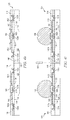
- FIG. 1 a shows a conventional semiconductor package 10 with a semiconductor die 12 having an active surface 14 .
- Conductive layer 16 are formed on active surface 14 .
- An insulating layer 18 is formed over active surface 14 and conductive layer 16 .
- An insulating layer 20 is formed over insulating layer 18 and conductive layer 16 .
- Conductive layer or redistribution layer (RDL) 22 is formed over insulating layer 20 and electrically connected to conductive layer 16 .
- An insulating layer 24 is formed over insulating layer 20 and conductive layer 22 .
- An under bump metallization (UBM) layer 26 is formed over insulating layer 24 and electrically connected to conductive layer 22 .
- a bump 28 is formed over UBM layer 26 .
- UBM under bump metallization
- FIG. 1 b is a plan view of semiconductor die 12 with a plurality of bumps 28 .
- Bump 28 a is enclosed by surrounding bumps 28 b .
- conductive layer 22 is routed between adjacent surrounding bumps 28 b .
- the routing arrangement of conductive layer 22 between adjacent surrounding bumps 28 b requires additional area on semiconductor die 12 .
- the adjacent surrounding bumps 28 b must be spaced further apart to permit the routing of conductive layer 22 between the bumps.
- routing conductive layer 22 between adjacent surrounding bumps 28 b makes die space allocation difficult.
- the present invention is a method of making a semiconductor device comprising the steps of providing a semiconductor wafer having a plurality of semiconductor die, forming a first conductive layer over a surface of the semiconductor wafer, forming a first insulating layer over the surface of the semiconductor wafer, forming a second conductive layer having first and second segments over the first insulating layer, forming a second insulating layer over the first insulating layer and second conductive layer, forming a third conductive layer over the second insulating layer and the first segment of the second conductive layer, forming a first bump over the third conductive layer, and forming a second bump over the surface of the semiconductor wafer electrically connected to the first segment of the second conductive layer.
- the first bump is electrically connected to the second segment of the second conductive layer and electrically isolated from the first segment of the second conductive layer.
- the present invention is a method of making a semiconductor device comprising the steps of providing a semiconductor die, forming a first insulating layer over a surface of the semiconductor die, forming a first conductive layer having first and second segments over the first insulating layer, forming a second insulating layer over the first insulating layer and first conductive layer, and forming a first interconnect structure over the first segment of the first conductive layer.
- the first interconnect structure is electrically connected to the second segment of the first conductive layer and electrically isolated from the first segment of the first conductive layer.
- the present invention is a method of making a semiconductor device comprising the steps of providing a semiconductor die, forming a first insulating layer over a surface of the semiconductor die, forming a first conductive layer over the first insulating layer, forming a second insulating layer over the first insulating layer and first conductive layer, and forming a first interconnect structure over the first conductive layer.
- the first interconnect structure is electrically isolated from the first conductive layer.
- the present invention is a semiconductor device comprising a semiconductor die and first insulating layer formed over a surface of the semiconductor die.
- a first conductive layer has first and second segments formed over the first insulating layer.
- a second insulating layer is formed over the first insulating layer and first conductive layer.
- a first interconnect structure is formed over the first segment of the first conductive layer. The first interconnect structure is electrically connected to the second segment of the first conductive layer and electrically isolated from the first segment of the first conductive layer.
- FIGS. 1 a - 1 b illustrate routing an RDL between adjacent surround bumps for electrical connection to an enclosed bump
- FIG. 2 illustrates a printed circuit board with different types of packages mounted to its surface
- FIGS. 3 a - 3 c illustrate further detail of the representative semiconductor packages mounted to the printed circuit board
- FIGS. 4 a - 4 i illustrate a process of forming an RDL under a bump for electrical connection to an enclosed bump
- FIGS. 5 a - 5 b illustrates a semiconductor die with an RDL formed under a bump for electrical connection to an enclosed bump.
- Front-end manufacturing involves the formation of a plurality of die on the surface of a semiconductor wafer.
- Each die on the wafer contains active and passive electrical components, which are electrically connected to form functional electrical circuits.
- Active electrical components such as transistors and diodes, have the ability to control the flow of electrical current.
- Passive electrical components such as capacitors, inductors, resistors, and transformers, create a relationship between voltage and current necessary to perform electrical circuit functions.
- Passive and active components are formed over the surface of the semiconductor wafer by a series of process steps including doping, deposition, photolithography, etching, and planarization.
- Doping introduces impurities into the semiconductor material by techniques such as ion implantation or thermal diffusion.
- the doping process modifies the electrical conductivity of semiconductor material in active devices, transforming the semiconductor material into an insulator, conductor, or dynamically changing the semiconductor material conductivity in response to an electric field or base current.
- Transistors contain regions of varying types and degrees of doping arranged as necessary to enable the transistor to promote or restrict the flow of electrical current upon the application of the electric field or base current.
- Active and passive components are formed by layers of materials with different electrical properties.
- the layers can be formed by a variety of deposition techniques determined in part by the type of material being deposited. For example, thin film deposition can involve chemical vapor deposition (CVD), physical vapor deposition (PVD), electrolytic plating, and electroless plating processes.
- CVD chemical vapor deposition
- PVD physical vapor deposition
- electrolytic plating electroless plating processes.
- Each layer is generally patterned to form portions of active components, passive components, or electrical connections between components.
- the layers can be patterned using photolithography, which involves the deposition of light sensitive material, e.g., photoresist, over the layer to be patterned.
- a pattern is transferred from a photomask to the photoresist using light.
- the portion of the photoresist pattern subjected to light is removed using a solvent, exposing portions of the underlying layer to be patterned.
- the portion of the photoresist pattern not subjected to light, the negative photoresist is removed using a solvent, exposing portions of the underlying layer to be patterned.
- the remainder of the photoresist is removed, leaving behind a patterned layer.
- some types of materials are patterned by directly depositing the material into the areas or voids formed by a previous deposition/etch process using techniques such as electroless and electrolytic plating.
- Patterning is the basic operation by which portions of the top layers on the semiconductor wafer surface are removed. Portions of the semiconductor wafer can be removed using photolithography, photomasking, masking, oxide or metal removal, photography and stenciling, and microlithography. Photolithography includes forming a pattern in reticles or a photomask and transferring the pattern into the surface layers of the semiconductor wafer. Photolithography forms the horizontal dimensions of active and passive components on the surface of the semiconductor wafer in a two-step process. First, the pattern on the reticle or masks is transferred into a layer of photoresist. Photoresist is a light-sensitive material that undergoes changes in structure and properties when exposed to light.
- the process of changing the structure and properties of the photoresist occurs as either negative-acting photoresist or positive-acting photoresist.
- the photoresist layer is transferred into the wafer surface. The transfer occurs when etching removes the portion of the top layers of semiconductor wafer not covered by the photoresist.
- the chemistry of photoresists is such that the photoresist remains substantially intact and resists removal by chemical etching solutions while the portion of the top layers of the semiconductor wafer not covered by the photoresist is removed.
- the process of forming, exposing, and removing the photoresist, as well as the process of removing a portion of the semiconductor wafer can be modified according to the particular resist used and the desired results.
- photoresist In negative-acting photoresists, photoresist is exposed to light and is changed from a soluble condition to an insoluble condition in a process known as polymerization. In polymerization, unpolymerized material is exposed to a light or energy source and polymers form a cross-linked material that is etch-resistant. In most negative resists, the polymers are polyisopremes. Removing the soluble portions (i.e. the portions not exposed to light) with chemical solvents or developers leaves a hole in the resist layer that corresponds to the opaque pattern on the reticle. A mask whose pattern exists in the opaque regions is called a clear-field mask.
- photoresist In positive-acting photoresists, photoresist is exposed to light and is changed from relatively nonsoluble condition to much more soluble condition in a process known as photosolubilization. In photosolubilization the relatively insoluble resist is exposed to the proper light energy and is converted to a more soluble state. The photosolubilized part of the resist can be removed by a solvent in the development process.
- the basic positive photoresist polymer is the phenol-formaldehyde polymer, also called the phenol-formaldehyde novolak resin. Removing the soluble portions (i.e. the portions exposed to light) with chemical solvents or developers leaves a hole in the resist layer that corresponds to the transparent pattern on the reticle. A mask whose pattern exists in the transparent regions is called a dark-field mask.
- the remainder of the photoresist is removed, leaving behind a patterned layer.
- some types of materials are patterned by directly depositing the material into the areas or voids formed by a previous deposition/etch process using techniques such as electroless and electrolytic plating.
- Planarization can be used to remove material from the surface of the wafer and produce a uniformly flat surface. Planarization involves polishing the surface of the wafer with a polishing pad. An abrasive material and corrosive chemical are added to the surface of the wafer during polishing. The combined mechanical action of the abrasive and corrosive action of the chemical removes any irregular topography, resulting in a uniformly flat surface.
- Back-end manufacturing refers to cutting or singulating the finished wafer into the individual semiconductor die and then packaging the semiconductor die for structural support and environmental isolation.
- the wafer is scored and broken along non-functional regions of the wafer called saw streets or scribes.
- the wafer is singulated using a laser cutting tool or saw blade.
- the individual semiconductor die are mounted to a package substrate that includes pins or contact pads for interconnection with other system components. Contact pads formed over the semiconductor die are then connected to contact pads within the package.
- the electrical connections can be made with solder bumps, stud bumps, conductive paste, or wirebonds.
- An encapsulant or other molding material is deposited over the package to provide physical support and electrical isolation. The finished package is then inserted into an electrical system and the functionality of the semiconductor device is made available to the other system components.
- FIG. 2 illustrates electronic device 50 having a chip carrier substrate or printed circuit board (PCB) 52 with a plurality of semiconductor packages mounted on its surface.
- Electronic device 50 can have one type of semiconductor package, or multiple types of semiconductor packages, depending on the application. The different types of semiconductor packages are shown in FIG. 2 for purposes of illustration.
- Electronic device 50 can be a stand-alone system that uses the semiconductor packages to perform one or more electrical functions.
- electronic device 50 can be a subcomponent of a larger system.
- electronic device 50 can be part of a cellular phone, personal digital assistant (PDA), digital video camera (DVC), or other electronic communication device.
- PDA personal digital assistant
- DVC digital video camera
- electronic device 50 can be a graphics card, network interface card, or other signal processing card that can be inserted into a computer.
- the semiconductor package can include microprocessors, memories, application specific integrated circuits (ASIC), logic circuits, analog circuits, RF circuits, discrete devices, or other semiconductor die or electrical components. Miniaturization and weight reduction are essential for these products to be accepted by the market. The distance between semiconductor devices must be decreased to achieve higher density.
- PCB 52 provides a general substrate for structural support and electrical interconnect of the semiconductor packages mounted on the PCB.
- Conductive signal traces 54 are formed over a surface or within layers of PCB 52 using evaporation, electrolytic plating, electroless plating, screen printing, or other suitable metal deposition process. Signal traces 54 provide for electrical communication between each of the semiconductor packages, mounted components, and other external system components. Traces 54 also provide power and ground connections to each of the semiconductor packages.
- a semiconductor device has two packaging levels.
- First level packaging is a technique for mechanically and electrically attaching the semiconductor die to an intermediate carrier.
- Second level packaging involves mechanically and electrically attaching the intermediate carrier to the PCB.
- a semiconductor device may only have the first level packaging where the die is mechanically and electrically mounted directly to the PCB.
- first level packaging including bond wire package 56 and flipchip 58
- second level packaging including ball grid array (BGA) 60 , bump chip carrier (BCC) 62 , dual in-line package (DIP) 64 , land grid array (LGA) 66 , multi-chip module (MCM) 68 , quad flat non-leaded package (QFN) 70 , and quad flat package 72 .
- BGA ball grid array
- BCC bump chip carrier
- DIP dual in-line package
- LGA land grid array
- MCM multi-chip module
- QFN quad flat non-leaded package
- quad flat package 72 quad flat package
- electronic device 50 includes a single attached semiconductor package, while other embodiments call for multiple interconnected packages.
- manufacturers can incorporate pre-made components into electronic devices and systems. Because the semiconductor packages include sophisticated functionality, electronic devices can be manufactured using less expensive components and a streamlined manufacturing process. The resulting devices are less likely to fail and less expensive to manufacture resulting in a lower cost for consumers.
- FIGS. 3 a - 3 c show exemplary semiconductor packages.
- FIG. 3 a illustrates further detail of DIP 64 mounted on PCB 52 .
- Semiconductor die 74 includes an active region containing analog or digital circuits implemented as active devices, passive devices, conductive layers, and dielectric layers formed within the die and are electrically interconnected according to the electrical design of the die.
- the circuit can include one or more transistors, diodes, inductors, capacitors, resistors, and other circuit elements formed within the active region of semiconductor die 74 .
- Contact pads 76 are one or more layers of conductive material, such as aluminum (Al), copper (Cu), tin (Sn), nickel (Ni), gold (Au), or silver (Ag), and are electrically connected to the circuit elements formed within semiconductor die 74 .
- semiconductor die 74 is mounted to an intermediate carrier 78 using a gold-silicon eutectic layer or adhesive material such as thermal epoxy or epoxy resin.
- the package body includes an insulative packaging material such as polymer or ceramic.
- Conductor leads 80 and bond wires 82 provide electrical interconnect between semiconductor die 74 and PCB 52 .
- Encapsulant 84 is deposited over the package for environmental protection by preventing moisture and particles from entering the package and contaminating semiconductor die 74 or bond wires 82 .
- FIG. 3 b illustrates further detail of BCC 62 mounted on PCB 52 .
- Semiconductor die 88 is mounted over carrier 90 using an underfill or epoxy-resin adhesive material 92 .
- Bond wires 94 provide first level packaging interconnect between contact pads 96 and 98 .
- Molding compound or encapsulant 100 is deposited over semiconductor die 88 and bond wires 94 to provide physical support and electrical isolation for the device.
- Contact pads 102 are formed over a surface of PCB 52 using a suitable metal deposition process such as electrolytic plating or electroless plating to prevent oxidation.
- Contact pads 102 are electrically connected to one or more conductive signal traces 54 in PCB 52 .
- Bumps 104 are formed between contact pads 98 of BCC 62 and contact pads 102 of PCB 52 .
- semiconductor die 58 is mounted face down to intermediate carrier 106 with a flipchip style first level packaging.
- Active region 108 of semiconductor die 58 contains analog or digital circuits implemented as active devices, passive devices, conductive layers, and dielectric layers formed according to the electrical design of the die.
- the circuit can include one or more transistors, diodes, inductors, capacitors, resistors, and other circuit elements within active region 108 .
- Semiconductor die 58 is electrically and mechanically connected to carrier 106 through bumps 110 .
- BGA 60 is electrically and mechanically connected to PCB 52 with a BGA style second level packaging using bumps 112 .
- Semiconductor die 58 is electrically connected to conductive signal traces 54 in PCB 52 through bumps 110 , signal lines 114 , and bumps 112 .
- a molding compound or encapsulant 116 is deposited over semiconductor die 58 and carrier 106 to provide physical support and electrical isolation for the device.
- the flipchip semiconductor device provides a short electrical conduction path from the active devices on semiconductor die 58 to conduction tracks on PCB 52 in order to reduce signal propagation distance, lower capacitance, and improve overall circuit performance.
- the semiconductor die 58 can be mechanically and electrically connected directly to PCB 52 using flipchip style first level packaging without intermediate carrier 106 .
- FIGS. 4 a - 4 i illustrate, in relation to FIG. 2 and FIGS. 3 a - 3 c , a process of forming an RDL under a bump for electrical connection to an enclosed bump.
- FIG. 4 a shows a semiconductor wafer 120 with a base substrate material 122 , such as silicon, germanium, gallium arsenide, indium phosphide, or silicon carbide, for structural support.
- a plurality of semiconductor die or components 124 is formed on wafer 120 separated by a non-active, inter-die wafer area or saw street 126 as described above. Saw street 126 provides cutting areas to singulate semiconductor wafer 120 into individual semiconductor die 124 .
- FIG. 4 b shows a cross-sectional view of a portion of semiconductor wafer 120 .
- Each semiconductor die 124 has a back surface 128 and active surface 130 containing analog or digital circuits implemented as active devices, passive devices, conductive layers, and dielectric layers formed within the die and electrically interconnected according to the electrical design and function of the die.
- the circuit may include one or more transistors, diodes, and other circuit elements formed within active surface 130 to implement analog circuits or digital circuits, such as digital signal processor (DSP), ASIC, memory, or other signal processing circuit.
- DSP digital signal processor
- Semiconductor die 124 may also contain integrated passive devices (IPDs), such as inductors, capacitors, and resistors, for RF signal processing.
- IPDs integrated passive devices
- semiconductor die 124 is a flipchip type device.
- An electrically conductive layer 132 is formed over active surface 130 using a patterning and metal deposition process, such as PVD, CVD, electrolytic plating, or electroless plating process.
- Conductive layer 132 can be one or more layers of Al, Cu, Sn, Ni, Au, Ag, or other suitable electrically conductive material.
- Conductive layer 132 is patterned into electrically isolated or electrically common segments 132 a - 132 f , each operating as a contact pad electrically connected to the circuits on active surface 130 .
- Contact pads 132 can be disposed side-by-side a first distance from the edge of semiconductor die 124 , as shown in FIG. 4 b .
- contact pads 132 can be offset in multiple rows such that a first row of contact pads is disposed a first distance from the edge of the die, and a second row of contact pads alternating with the first row is disposed a second distance from the edge of the die.
- an insulating or passivation layer 134 is conformally applied over active surface 130 and conductive layer 132 a - 132 f using PVD, CVD, printing, spin coating, spray coating, sintering or thermal oxidation.
- the insulating layer 134 contains one or more layers of silicon dioxide (SiO2), silicon nitride (Si3N4), silicon oxynitride (SiON), tantalum pentoxide (Ta2O5), aluminum oxide (Al2O3, or other material having similar insulating and structural properties.
- the insulating layer 134 follows the contour of active surface 130 and conductive layer 132 a - 132 f .
- a portion of insulating layer 134 is removed by an etching process through a patterned photoresist layer (not shown) to form openings 136 and expose conductive layer 132 a , 132 c , 132 d , and 132 f .
- openings 136 are formed by laser direct ablation (LDA) using laser 138 to remove a portion of insulating layer 134 and expose conductive layer 132 a , 132 c , 132 d , and 132 f .
- LDA laser direct ablation
- a portion of conductive layer 132 a , 132 c , 132 d , and 132 f remains covered by insulating layer 134 .
- an insulating or passivation layer 140 is formed over insulating layer 134 and conductive layer 132 a , 132 c , 132 d , and 132 f using PVD, CVD, printing, spin coating, spray coating, sintering or thermal oxidation.
- the insulating layer 140 contains one or more layers of SiO2, Si3N4, SiON, Ta2O5, Al2O3, or other material having similar insulating and structural properties.
- a portion of insulating layer 140 is removed by an etching process through a patterned photoresist layer to expose conductive layer 132 a , 132 c , 132 d , and 132 f .
- conductive layer 132 a , 132 c , 132 d , and 132 f is exposed by LDA using laser 138 . A portion of conductive layer 132 a , 132 c , 132 d , and 132 f remains covered by insulating layer 140 .
- an electrically conductive layer 142 is conformally applied over insulating layer 140 and conductive layer 132 a , 132 c , 132 d , and 132 f using a patterning and metal deposition process, such as PVD, CVD, electrolytic plating, or electroless plating process.
- Conductive layer 142 can be one or more layers of Al, Cu, Sn, Ni, Au, Ag, or other suitable electrically conductive material.
- Conductive layer 142 follows the contour of insulating layer 140 and conductive layer 132 a , 132 c , 132 d , and 132 f .
- Conductive layer 142 is patterned into a plurality of segments 142 a - 142 f operating as RDL to laterally redistribute the electrical interconnect to conductive layer 132 . Portions of conductive layer 142 a - 142 c are coplanar with a surface of insulating layer 140 , and portions of conductive layer 142 d - 142 f are coplanar with a surface of insulating layer 140 .
- Conductive layer 142 a is electrically connected to conductive layer 132 a .
- Conductive layer 142 b is electrically isolated from conductive layer 142 a , 142 c , and 132 b by insulating layer 140 .
- Conductive layer 142 c is electrically connected to conductive layer 132 c .
- Conductive layer 142 d is electrically connected to conductive layer 132 d .
- Conductive layer 142 e is electrically isolated from conductive layer 142 d , 142 f , and 132 e by insulating layer 140 .
- Conductive layer 142 f is electrically connected to conductive layer 132 f.
- FIG. 4 f shows a plan view of conductive layer 142 a - 142 f .
- Conductive layer 142 b is routed between conductive layer 142 a and 142 c
- conductive layer 142 e is routed between conductive layer 142 d and 142 f .
- width W 142b of conductive layer 142 b of 15 micrometers ( ⁇ m)
- width W 142a -W 142c between conductive layer 142 a and 142 c is 45 ⁇ m.
- W 142e of conductive layer 142 e of 15 ⁇ m the width W 142d -W 142f between conductive layer 142 e and 142 f is 45 ⁇ m.
- an insulating or passivation layer 144 is formed over insulating layer 140 and conductive layer 142 a - 142 f using PVD, CVD, printing, spin coating, spray coating, sintering or thermal oxidation.
- the insulating layer 144 contains one or more layers of SiO2, Si3N4, SiON, Ta2O5, Al2O3, or other material having similar insulating and structural properties.
- insulating layer 144 has a thickness 5-10 ⁇ m. A portion of insulating layer 144 is removed by an etching process through a photoresist layer to expose conductive layer 142 a , 142 c , 142 d , and 142 f .
- conductive layer 142 a , 142 c , 142 d , and 142 f is exposed by LDA using laser 138 .
- Conductive layer 142 b and 142 e remains covered by insulating layer 144 and electrically isolated from conductive layer 132 b and 132 e and conductive layer 142 a , 142 c , 142 d , and 142 f by insulating layers 140 and 144 .
- an electrically conductive layer 146 is conformally applied over insulating layer 144 and the exposed conductive layer 142 a , 142 c , 142 d , and 142 f using a patterning and metal deposition process such as printing, PVD, CVD, sputtering, electrolytic plating, and electroless plating.
- Conductive layer 146 can be one or more layers of Al, Cu, Sn, Ti, Ni, Au, Ag, or other suitable electrically conductive material.
- Conductive layer 146 has a width of 250-300 ⁇ m and follows the contour of insulating layer 144 and the exposed conductive layer 142 a , 142 c , 142 d , and 142 f .
- conductive layer 146 is a multi-layer stack UBM layer including a seed layer, barrier layer, and adhesion layer.
- the seed layer can be titanium copper (TiCu), titanium tungsten copper (TiWCu), or tantalum nitrogen copper (TaNCu).
- the barrier layer can be Ni, nickel vanadium (NiV), platinum (Pt), palladium (Pd), TiW, or CrCu, or other suitable material.
- the adhesion layer can be Ti, TiN, TiW, Al, or chromium (Cr), or other suitable material.
- Conductive layer 146 is electrically connected to conductive layer 142 a , 142 c , 142 d , and 142 f .
- Conductive layer 146 is electrically isolated from conductive layer 142 b and 142 e by insulating layer 144 .
- an electrically conductive bump material is deposited over conductive layer 146 using an evaporation, electrolytic plating, electroless plating, ball drop, or screen printing process.
- the bump material can be Al, Sn, Ni, Au, Ag, Pb, Bi, Cu, solder, and combinations thereof, with an optional flux solution.
- the bump material can be eutectic Sn/Pb, high-lead solder, or lead-free solder.
- the bump material is bonded to conductive layer 146 using a suitable attachment or bonding process. In one embodiment, the bump material is reflowed by heating the material above its melting point to form balls or bumps 148 .
- bumps 148 are reflowed a second time to improve electrical contact to conductive layer 146 .
- Bumps 148 can also be compression bonded to conductive layer 146 .
- Bumps 148 represent one type of interconnect structure that can be formed over conductive layer 146 .
- the interconnect structure can also use stud bump, micro bump, or other electrical interconnect.
- Semiconductor wafer 120 is singulated through saw street 126 with saw blade or laser cutting tool 150 into individual semiconductor die 124 .
- FIGS. 5 a - 5 b shows semiconductor die 124 after singulation.
- the circuits on active surface 130 are electrically connected to conductive layer 132 a - 132 f .
- Conductive layer 132 a , 132 c , 132 d , and 132 f is electrically connected to conductive layer 142 a , 142 c , 142 d , and 142 f , conductive layer 146 , and bumps 148 , as shown in FIG. 5 a .
- FIG. 5 b shows bump 148 a disposed in an interior region of semiconductor die 124 and surrounded by bumps 148 b .
- Conductive layer 142 b and 142 e is electrically connected to bump 148 a by routing conductive layer 142 b and 142 e beneath conductive layer 146 and bump 148 .
- the routing arrangement with conductive layer 142 b and 142 e disposed beneath conductive layer 146 and bump 148 reduces the area required for routing and simplifies the routing configuration, particularly for interior contact pads and bumps enclosed by other interconnect structures.
- Conductive layer 142 b and 142 e is electrically isolated from conductive layer 146 and bump 148 b by nature of insulating layer 144 .
- a semiconductor wafer 120 has a plurality of semiconductor die 124 .
- Conductive layer 132 is formed over a surface of semiconductor wafer 120 .
- the insulating layer 134 is formed over the surface of semiconductor wafer 120 and conductive layer 132 .
- the insulating layer 140 is formed over insulating layer 134 and conductive layer 132 .
- a portion of insulating layer 140 is removed by LDA.
- Conductive layer 142 has segments 142 a and 142 b formed over insulating layer 140 .
- the segment 142 a and segment 142 b of conductive layer 142 are coplanar with a surface of insulating layer 140 .
- the segment 142 b has a width of 15 ⁇ m.
- the insulating layer 144 is formed over insulating layer 140 and conductive layer 142 .
- Conductive layer 146 is formed over insulating layer 144 and segment 142 b of conductive layer 140 .
- Bumps 148 a and 148 b are formed over conductive layer 146 with interior bump 148 a surrounded by bumps 148 b .
- Bump 148 b is electrically connected to segment 142 a and electrically isolated from segment 142 b by insulating layer 144 .
- conductive layer 142 b is routed beneath bump 148 b separated by insulating layer 144 .
- Bump 148 a is electrically connected to segment 142 b of conductive layer 142 .
- the segment 142 b is electrically isolated from conductive layer 146 by insulating layer 144 .
Abstract
Description
Claims (19)
Priority Applications (1)
| Application Number | Priority Date | Filing Date | Title |
|---|---|---|---|
| US13/307,849 US9142522B2 (en) | 2011-11-30 | 2011-11-30 | Semiconductor device and method of forming RDL under bump for electrical connection to enclosed bump |
Applications Claiming Priority (1)
| Application Number | Priority Date | Filing Date | Title |
|---|---|---|---|
| US13/307,849 US9142522B2 (en) | 2011-11-30 | 2011-11-30 | Semiconductor device and method of forming RDL under bump for electrical connection to enclosed bump |
Publications (2)
| Publication Number | Publication Date |
|---|---|
| US20130134580A1 US20130134580A1 (en) | 2013-05-30 |
| US9142522B2 true US9142522B2 (en) | 2015-09-22 |
Family
ID=48466081
Family Applications (1)
| Application Number | Title | Priority Date | Filing Date |
|---|---|---|---|
| US13/307,849 Active 2032-06-08 US9142522B2 (en) | 2011-11-30 | 2011-11-30 | Semiconductor device and method of forming RDL under bump for electrical connection to enclosed bump |
Country Status (1)
| Country | Link |
|---|---|
| US (1) | US9142522B2 (en) |
Cited By (1)
| Publication number | Priority date | Publication date | Assignee | Title |
|---|---|---|---|---|
| US10580726B2 (en) | 2017-11-02 | 2020-03-03 | Samsung Electronics Co., Ltd. | Semiconductor devices and semiconductor packages including the same, and methods of manufacturing the semiconductor devices |
Families Citing this family (4)
| Publication number | Priority date | Publication date | Assignee | Title |
|---|---|---|---|---|
| KR101429347B1 (en) * | 2012-08-30 | 2014-08-12 | 앰코 테크놀로지 코리아 주식회사 | Semiconductor package and fabricating method thereof |
| WO2014112954A1 (en) * | 2013-01-21 | 2014-07-24 | Pbt Pte. Ltd. | Substrate for semiconductor packaging and method of forming same |
| US9349700B2 (en) | 2013-04-24 | 2016-05-24 | Stats Chippac, Ltd. | Semiconductor device and method of forming stress-reduced conductive joint structures |
| US9184143B2 (en) * | 2013-12-05 | 2015-11-10 | Taiwan Semiconductor Manufacturing Company Ltd. | Semiconductor device with bump adjustment and manufacturing method thereof |
Citations (5)
| Publication number | Priority date | Publication date | Assignee | Title |
|---|---|---|---|---|
| US6727118B2 (en) * | 2002-02-06 | 2004-04-27 | International Business Machines Corporation | Power distribution design method for stacked flip-chip packages |
| US20060057834A1 (en) * | 2002-11-15 | 2006-03-16 | Sharp Kabushiki Kaisha | Semiconductor device and fabrication process thereof |
| US7642128B1 (en) | 2008-12-12 | 2010-01-05 | Stats Chippac, Ltd. | Semiconductor device and method of forming a vertical interconnect structure for 3-D FO-WLCSP |
| US7952203B2 (en) | 2008-08-29 | 2011-05-31 | Intel Corporation | Methods of forming C4 round dimple metal stud bumps for fine pitch packaging applications and structures formed thereby |
| US20110156248A1 (en) * | 2009-12-25 | 2011-06-30 | Fujitsu Semiconductor Limited | Semiconductor device and method for manufacturing the same |
-
2011
- 2011-11-30 US US13/307,849 patent/US9142522B2/en active Active
Patent Citations (5)
| Publication number | Priority date | Publication date | Assignee | Title |
|---|---|---|---|---|
| US6727118B2 (en) * | 2002-02-06 | 2004-04-27 | International Business Machines Corporation | Power distribution design method for stacked flip-chip packages |
| US20060057834A1 (en) * | 2002-11-15 | 2006-03-16 | Sharp Kabushiki Kaisha | Semiconductor device and fabrication process thereof |
| US7952203B2 (en) | 2008-08-29 | 2011-05-31 | Intel Corporation | Methods of forming C4 round dimple metal stud bumps for fine pitch packaging applications and structures formed thereby |
| US7642128B1 (en) | 2008-12-12 | 2010-01-05 | Stats Chippac, Ltd. | Semiconductor device and method of forming a vertical interconnect structure for 3-D FO-WLCSP |
| US20110156248A1 (en) * | 2009-12-25 | 2011-06-30 | Fujitsu Semiconductor Limited | Semiconductor device and method for manufacturing the same |
Cited By (1)
| Publication number | Priority date | Publication date | Assignee | Title |
|---|---|---|---|---|
| US10580726B2 (en) | 2017-11-02 | 2020-03-03 | Samsung Electronics Co., Ltd. | Semiconductor devices and semiconductor packages including the same, and methods of manufacturing the semiconductor devices |
Also Published As
| Publication number | Publication date |
|---|---|
| US20130134580A1 (en) | 2013-05-30 |
Similar Documents
| Publication | Publication Date | Title |
|---|---|---|
| US9117812B2 (en) | Semiconductor device and method of forming non-linear interconnect layer with extended length for joint reliability | |
| US9397058B2 (en) | Semiconductor device and method of forming patterned repassivation openings between RDL and UBM to reduce adverse effects of electro-migration | |
| US9607958B2 (en) | Semiconductor device and method for forming openings and trenches in insulating layer by first LDA and second LDA for RDL formation | |
| US9252094B2 (en) | Semiconductor device and method of forming an interconnect structure with conductive material recessed within conductive ring over surface of conductive pillar | |
| US9601462B2 (en) | Semiconductor device and method of forming UBM structure on back surface of TSV semiconductor wafer | |
| US9824923B2 (en) | Semiconductor device and method of forming conductive pillar having an expanded base | |
| US9484259B2 (en) | Semiconductor device and method of forming protection and support structure for conductive interconnect structure | |
| US9837336B2 (en) | Semiconductor device and method of forming insulating layer in notches around conductive TSV for stress relief | |
| US9082832B2 (en) | Semiconductor device and method of forming protection and support structure for conductive interconnect structure | |
| US9202713B2 (en) | Semiconductor device and method of forming RDL over contact pad with high alignment tolerance or reduced interconnect pitch | |
| US9331007B2 (en) | Semiconductor device and method of forming conductive ink layer as interconnect structure between semiconductor packages | |
| US9478513B2 (en) | Semiconductor device with conductive pillars having recesses or protrusions to detect interconnect continuity between semiconductor die and substrate | |
| US20130249104A1 (en) | Semiconductor Device and Method of Forming Conductive Layer Over Metal Substrate for Electrical Interconnect of Semiconductor Die | |
| US9257382B2 (en) | Semiconductor device and method of forming guard ring around conductive TSV through semiconductor wafer | |
| US9054100B2 (en) | Semiconductor die and method of forming sloped surface in photoresist layer to enhance flow of underfill material between semiconductor die and substrate | |
| US9142522B2 (en) | Semiconductor device and method of forming RDL under bump for electrical connection to enclosed bump | |
| US20130147035A1 (en) | Semiconductor Device and Method of Forming Recesses in Conductive Layer to Detect Continuity for Interconnect Between Semiconductor Die and Substrate | |
| US9685415B2 (en) | Semiconductor device and method of forming micro-vias partially through insulating material around bump interconnect |
Legal Events
| Date | Code | Title | Description |
|---|---|---|---|
| AS | Assignment |
Owner name: STATS CHIPPAC, LTD., SINGAPORE Free format text: ASSIGNMENT OF ASSIGNORS INTEREST;ASSIGNORS:BAO, XUSHENG;PWINT, MA PHOO;ZUO, JIAN;REEL/FRAME:027303/0274 Effective date: 20111129 |
|
| AS | Assignment |
Owner name: CITICORP INTERNATIONAL LIMITED, AS COMMON SECURITY AGENT, HONG KONG Free format text: SECURITY INTEREST;ASSIGNORS:STATS CHIPPAC, INC.;STATS CHIPPAC LTD.;REEL/FRAME:036288/0748 Effective date: 20150806 Owner name: CITICORP INTERNATIONAL LIMITED, AS COMMON SECURITY Free format text: SECURITY INTEREST;ASSIGNORS:STATS CHIPPAC, INC.;STATS CHIPPAC LTD.;REEL/FRAME:036288/0748 Effective date: 20150806 |
|
| STCF | Information on status: patent grant |
Free format text: PATENTED CASE |
|
| AS | Assignment |
Owner name: STATS CHIPPAC PTE. LTE., SINGAPORE Free format text: CHANGE OF NAME;ASSIGNOR:STATS CHIPPAC LTD.;REEL/FRAME:038378/0418 Effective date: 20160329 |
|
| MAFP | Maintenance fee payment |
Free format text: PAYMENT OF MAINTENANCE FEE, 4TH YEAR, LARGE ENTITY (ORIGINAL EVENT CODE: M1551); ENTITY STATUS OF PATENT OWNER: LARGE ENTITY Year of fee payment: 4 |
|
| AS | Assignment |
Owner name: STATS CHIPPAC PTE. LTD. FORMERLY KNOWN AS STATS CH Free format text: RELEASE BY SECURED PARTY;ASSIGNOR:CITICORP INTERNATIONAL LIMITED, AS COMMON SECURITY AGENT;REEL/FRAME:051285/0318 Effective date: 20190503 Owner name: STATS CHIPPAC, INC., CALIFORNIA Free format text: RELEASE BY SECURED PARTY;ASSIGNOR:CITICORP INTERNATIONAL LIMITED, AS COMMON SECURITY AGENT;REEL/FRAME:051285/0318 Effective date: 20190503 Owner name: STATS CHIPPAC PTE. LTD. FORMERLY KNOWN AS STATS CHIPPAC LTD., SINGAPORE Free format text: RELEASE BY SECURED PARTY;ASSIGNOR:CITICORP INTERNATIONAL LIMITED, AS COMMON SECURITY AGENT;REEL/FRAME:051285/0318 Effective date: 20190503 |
|
| AS | Assignment |
Owner name: JCET SEMICONDUCTOR (SHAOXING) CO., LTD., CHINA Free format text: ASSIGNMENT OF ASSIGNORS INTEREST;ASSIGNOR:STATS CHIPPAC PTE. LTD.;REEL/FRAME:051365/0680 Effective date: 20191128 |
|
| MAFP | Maintenance fee payment |
Free format text: PAYMENT OF MAINTENANCE FEE, 8TH YEAR, LARGE ENTITY (ORIGINAL EVENT CODE: M1552); ENTITY STATUS OF PATENT OWNER: LARGE ENTITY Year of fee payment: 8 |
|
| AS | Assignment |
Owner name: STATS CHIPPAC PTE. LTD., SINGAPORE Free format text: CORRECTIVE ASSIGNMENT TO CORRECT THE ASSIGNEE'S NAME ON COVERSHEET FROM "STATS CHIPPAC PTE. LTE." TO "STATS CHIPPAC PTE. LTD." PREVIOUSLY RECORDED ON REEL 038378 FRAME 0418. ASSIGNOR(S) HEREBY CONFIRMS THE CHANGE OF NAME;ASSIGNOR:STATS CHIPPAC LTD.;REEL/FRAME:064908/0920 Effective date: 20160329 |