US9140428B2 - Triplet-triplet annihilation up-conversation for display and lighting applications - Google Patents

Triplet-triplet annihilation up-conversation for display and lighting applications Download PDF

Info

Publication number
US9140428B2
US9140428B2 US14/256,007 US201414256007A US9140428B2 US 9140428 B2 US9140428 B2 US 9140428B2 US 201414256007 A US201414256007 A US 201414256007A US 9140428 B2 US9140428 B2 US 9140428B2
Authority
US
United States
Prior art keywords
triplet
emitting device
light emitting
organic light
layer
Prior art date
Legal status (The legal status is an assumption and is not a legal conclusion. Google has not performed a legal analysis and makes no representation as to the accuracy of the status listed.)
Active
Application number
US14/256,007
Other versions
US20140226338A1 (en
Inventor
Chuanjun Xia
Michael Stuart Weaver
Jason Brooks
Current Assignee (The listed assignees may be inaccurate. Google has not performed a legal analysis and makes no representation or warranty as to the accuracy of the list.)
Universal Display Corp
Original Assignee
Universal Display Corp
Priority date (The priority date is an assumption and is not a legal conclusion. Google has not performed a legal analysis and makes no representation as to the accuracy of the date listed.)
Filing date
Publication date
Application filed by Universal Display Corp filed Critical Universal Display Corp
Priority to US14/256,007 priority Critical patent/US9140428B2/en
Assigned to UNIVERSAL DISPLAY CORPORATION reassignment UNIVERSAL DISPLAY CORPORATION ASSIGNMENT OF ASSIGNORS INTEREST (SEE DOCUMENT FOR DETAILS). Assignors: WEAVER, MICHAEL STUART, BROOKS, JASON, XIA, CHUANJUN
Publication of US20140226338A1 publication Critical patent/US20140226338A1/en
Application granted granted Critical
Publication of US9140428B2 publication Critical patent/US9140428B2/en
Active legal-status Critical Current
Anticipated expiration legal-status Critical

Links

Images

Classifications

    • HELECTRICITY
    • H10SEMICONDUCTOR DEVICES; ELECTRIC SOLID-STATE DEVICES NOT OTHERWISE PROVIDED FOR
    • H10KORGANIC ELECTRIC SOLID-STATE DEVICES
    • H10K59/00Integrated devices, or assemblies of multiple devices, comprising at least one organic light-emitting element covered by group H10K50/00
    • H10K59/30Devices specially adapted for multicolour light emission
    • H10K59/35Devices specially adapted for multicolour light emission comprising red-green-blue [RGB] subpixels
    • FMECHANICAL ENGINEERING; LIGHTING; HEATING; WEAPONS; BLASTING
    • F21LIGHTING
    • F21VFUNCTIONAL FEATURES OR DETAILS OF LIGHTING DEVICES OR SYSTEMS THEREOF; STRUCTURAL COMBINATIONS OF LIGHTING DEVICES WITH OTHER ARTICLES, NOT OTHERWISE PROVIDED FOR
    • F21V9/00Elements for modifying spectral properties, polarisation or intensity of the light emitted, e.g. filters
    • F21V9/08Elements for modifying spectral properties, polarisation or intensity of the light emitted, e.g. filters for producing coloured light, e.g. monochromatic; for reducing intensity of light
    • H01L27/3211
    • H01L27/322
    • HELECTRICITY
    • H10SEMICONDUCTOR DEVICES; ELECTRIC SOLID-STATE DEVICES NOT OTHERWISE PROVIDED FOR
    • H10KORGANIC ELECTRIC SOLID-STATE DEVICES
    • H10K59/00Integrated devices, or assemblies of multiple devices, comprising at least one organic light-emitting element covered by group H10K50/00
    • H10K59/30Devices specially adapted for multicolour light emission
    • H10K59/38Devices specially adapted for multicolour light emission comprising colour filters or colour changing media [CCM]
    • H01L51/0043
    • H01L51/0052
    • H01L51/0054
    • H01L51/0055
    • H01L51/0071
    • H01L51/0084
    • H01L51/0085
    • H01L51/0086
    • H01L51/0087
    • HELECTRICITY
    • H10SEMICONDUCTOR DEVICES; ELECTRIC SOLID-STATE DEVICES NOT OTHERWISE PROVIDED FOR
    • H10KORGANIC ELECTRIC SOLID-STATE DEVICES
    • H10K50/00Organic light-emitting devices
    • H10K50/10OLEDs or polymer light-emitting diodes [PLED]
    • H10K50/11OLEDs or polymer light-emitting diodes [PLED] characterised by the electroluminescent [EL] layers
    • H10K50/125OLEDs or polymer light-emitting diodes [PLED] characterised by the electroluminescent [EL] layers specially adapted for multicolour light emission, e.g. for emitting white light
    • HELECTRICITY
    • H10SEMICONDUCTOR DEVICES; ELECTRIC SOLID-STATE DEVICES NOT OTHERWISE PROVIDED FOR
    • H10KORGANIC ELECTRIC SOLID-STATE DEVICES
    • H10K85/00Organic materials used in the body or electrodes of devices covered by this subclass
    • H10K85/10Organic polymers or oligomers
    • H10K85/151Copolymers
    • HELECTRICITY
    • H10SEMICONDUCTOR DEVICES; ELECTRIC SOLID-STATE DEVICES NOT OTHERWISE PROVIDED FOR
    • H10KORGANIC ELECTRIC SOLID-STATE DEVICES
    • H10K85/00Organic materials used in the body or electrodes of devices covered by this subclass
    • H10K85/30Coordination compounds
    • H10K85/341Transition metal complexes, e.g. Ru(II)polypyridine complexes
    • H10K85/342Transition metal complexes, e.g. Ru(II)polypyridine complexes comprising iridium
    • HELECTRICITY
    • H10SEMICONDUCTOR DEVICES; ELECTRIC SOLID-STATE DEVICES NOT OTHERWISE PROVIDED FOR
    • H10KORGANIC ELECTRIC SOLID-STATE DEVICES
    • H10K85/00Organic materials used in the body or electrodes of devices covered by this subclass
    • H10K85/30Coordination compounds
    • H10K85/341Transition metal complexes, e.g. Ru(II)polypyridine complexes
    • H10K85/344Transition metal complexes, e.g. Ru(II)polypyridine complexes comprising ruthenium
    • HELECTRICITY
    • H10SEMICONDUCTOR DEVICES; ELECTRIC SOLID-STATE DEVICES NOT OTHERWISE PROVIDED FOR
    • H10KORGANIC ELECTRIC SOLID-STATE DEVICES
    • H10K85/00Organic materials used in the body or electrodes of devices covered by this subclass
    • H10K85/30Coordination compounds
    • H10K85/341Transition metal complexes, e.g. Ru(II)polypyridine complexes
    • H10K85/346Transition metal complexes, e.g. Ru(II)polypyridine complexes comprising platinum
    • HELECTRICITY
    • H10SEMICONDUCTOR DEVICES; ELECTRIC SOLID-STATE DEVICES NOT OTHERWISE PROVIDED FOR
    • H10KORGANIC ELECTRIC SOLID-STATE DEVICES
    • H10K85/00Organic materials used in the body or electrodes of devices covered by this subclass
    • H10K85/60Organic compounds having low molecular weight
    • H10K85/615Polycyclic condensed aromatic hydrocarbons, e.g. anthracene
    • H10K85/622Polycyclic condensed aromatic hydrocarbons, e.g. anthracene containing four rings, e.g. pyrene
    • HELECTRICITY
    • H10SEMICONDUCTOR DEVICES; ELECTRIC SOLID-STATE DEVICES NOT OTHERWISE PROVIDED FOR
    • H10KORGANIC ELECTRIC SOLID-STATE DEVICES
    • H10K85/00Organic materials used in the body or electrodes of devices covered by this subclass
    • H10K85/60Organic compounds having low molecular weight
    • H10K85/615Polycyclic condensed aromatic hydrocarbons, e.g. anthracene
    • H10K85/623Polycyclic condensed aromatic hydrocarbons, e.g. anthracene containing five rings, e.g. pentacene
    • HELECTRICITY
    • H10SEMICONDUCTOR DEVICES; ELECTRIC SOLID-STATE DEVICES NOT OTHERWISE PROVIDED FOR
    • H10KORGANIC ELECTRIC SOLID-STATE DEVICES
    • H10K85/00Organic materials used in the body or electrodes of devices covered by this subclass
    • H10K85/60Organic compounds having low molecular weight
    • H10K85/649Aromatic compounds comprising a hetero atom
    • H10K85/657Polycyclic condensed heteroaromatic hydrocarbons

Definitions

  • the claimed invention was made by, on behalf of, and/or in connection with one or more of the following parties to a joint university corporation research agreement: Regents of the University of Michigan, Princeton University, The University of Southern California, and the Universal Display Corporation. The agreement was in effect on and before the date the claimed invention was made, and the claimed invention was made as a result of activities undertaken within the scope of the agreement.
  • the present invention relates to organic light emitting devices (OLEDs). More specifically, the present invention pertains to devices comprising a layer of compounds capable of triplet triplet annihilation up-conversation (TTA-UC) such that emission is converted to a shorter wavelength.
  • OLEDs organic light emitting devices
  • TTA-UC triplet triplet annihilation up-conversation
  • Opto-electronic devices that make use of organic materials are becoming increasingly desirable for a number of reasons. Many of the materials used to make such devices are relatively inexpensive, so organic opto-electronic devices have the potential for cost advantages over inorganic devices. In addition, the inherent properties of organic materials, such as their flexibility, may make them well suited for particular applications such as fabrication on a flexible substrate. Examples of organic opto-electronic devices include organic light emitting devices (OLEDs), organic phototransistors, organic photovoltaic cells, and organic photodetectors. For OLEDs, the organic materials may have performance advantages over conventional materials. For example, the wavelength at which an organic emissive layer emits light may generally be readily tuned with appropriate dopants.
  • OLEDs organic light emitting devices
  • the wavelength at which an organic emissive layer emits light may generally be readily tuned with appropriate dopants.
  • OLEDs make use of thin organic films that emit light when voltage is applied across the device. OLEDs are becoming an increasingly interesting technology for use in applications such as flat panel displays, illumination, and backlighting. Several OLED materials and configurations are described in U.S. Pat. Nos. 5,844,363, 6,303,238, and 5,707,745, which are incorporated herein by reference in their entirety.
  • phosphorescent emissive molecules is a full color display.
  • Industry standards for such a display call for pixels adapted to emit particular colors, referred to as “saturated” colors.
  • these standards call for saturated red, green, and blue pixels. Color may be measured using CIE coordinates, which are well known to the art.
  • a green emissive molecule is tris(2-phenylpyridine) iridium, denoted Ir(ppy) 3 , which has the structure:
  • organic includes polymeric materials as well as small molecule organic materials that may be used to fabricate organic opto-electronic devices.
  • Small molecule refers to any organic material that is not a polymer, and “small molecules” may actually be quite large. Small molecules may include repeat units in some circumstances. For example, using a long chain alkyl group as a substituent does not remove a molecule from the “small molecule” class. Small molecules may also be incorporated into polymers, for example as a pendent group on a polymer backbone or as a part of the backbone. Small molecules may also serve as the core moiety of a dendrimer, which consists of a series of chemical shells built on the core moiety.
  • the core moiety of a dendrimer may be a fluorescent or phosphorescent small molecule emitter.
  • a dendrimer may be a “small molecule,” and it is believed that all dendrimers currently used in the field of OLEDs are small molecules.
  • top means furthest away from the substrate, while “bottom” means closest to the substrate.
  • first layer is described as “disposed over” a second layer, the first layer is disposed further away from substrate. There may be other layers between the first and second layer, unless it is specified that the first layer is “in contact with” the second layer.
  • a cathode may be described as “disposed over” an anode, even though there are various organic layers in between.
  • solution processible means capable of being dissolved, dispersed, or transported in and/or deposited from a liquid medium, either in solution or suspension form.
  • a ligand may be referred to as “photoactive” when it is believed that the ligand directly contributes to the photoactive properties of an emissive material.
  • a ligand may be referred to as “ancillary” when it is believed that the ligand does not contribute to the photoactive properties of an emissive material, although an ancillary ligand may alter the properties of a photoactive ligand.
  • a first “Highest Occupied Molecular Orbital” (HOMO) or “Lowest Unoccupied Molecular Orbital” (LUMO) energy level is “greater than” or “higher than” a second HOMO or LUMO energy level if the first energy level is closer to the vacuum energy level.
  • IP ionization potentials
  • a higher HOMO energy level corresponds to an IP having a smaller absolute value (an IP that is less negative).
  • a higher LUMO energy level corresponds to an electron affinity (EA) having a smaller absolute value (an EA that is less negative).
  • the LUMO energy level of a material is higher than the HOMO energy level of the same material.
  • a “higher” HOMO or LUMO energy level appears closer to the top of such a diagram than a “lower” HOMO or LUMO energy level.
  • a first work function is “greater than” or “higher than” a second work function if the first work function has a higher absolute value. Because work functions are generally measured as negative numbers relative to vacuum level, this means that a “higher” work function is more negative. On a conventional energy level diagram, with the vacuum level at the top, a “higher” work function is illustrated as further away from the vacuum level in the downward direction. Thus, the definitions of HOMO and LUMO energy levels follow a different convention than work functions.
  • a first device comprising a first organic light emitting device comprising a first material that is an emitting material having a first emissive spectrum, and a first triplet-triplet annihilation up-conversation layer disposed adjacent to the first organic light emitting device such that light emitted by the organic light emitting device is incident on the first up-conversation layer.
  • the first triplet-triplet annihilation up-conversation layer comprising a first donor material and a first acceptor material, and the first donor material has an absorption spectrum that overlaps with the first emissive spectrum.
  • the device further comprises a pixel, which further comprises three subpixels.
  • the first subpixel comprises the first organic light emitting device and the first up-conversation layer disposed adjacent to the first organic light emitting device.
  • the second subpixel comprises a second organic light emitting device comprising a second material that is an emitting material having a second emissive spectrum.
  • the second subpixel does not include an up-conversation layer or a down conversion layer.
  • the third subpixel comprises a third organic light emitting device comprising a third material that is an emitting material having a third emissive spectrum.
  • the third subpixel further comprises a first down conversion layer disposed adjacent to the third organic light emitting device such that light emitted by the third organic light emitting device is incident on the first down conversion layer.
  • the first material, the second material, and the third material have an emissive spectrum having a peak wavelength of about 500 nm to about 600 nm.
  • the first material, the second material, and the third material are the same material.
  • the first and the second materials have an emissive spectrum having a peak wavelength of about 500 nm to about 600 nm
  • the third material has an emissive spectrum having a peak wavelength of about 600 nm to about 700 nm.
  • the second subpixel does not comprise an up-conversation layer or a down conversion layer.
  • the first subpixel has an emissive spectrum that has a peak wavelength of about 400 nm to about 500 nm
  • the second subpixel has an emissive spectrum that has a peak wavelength of about 500 nm to about 600 nm
  • the third subpixel has an emissive spectrum that has a peak wavelength of about 600 nm to about 700 nm.
  • the first material, the second material, and the third material have an emissive spectrum having a peak wavelength of about 500 nm to about 600 nm.
  • the first material emits light having a peak wavelength of about 500 to about 600 nm.
  • the first up-conversation layer absorbs light having a peak wavelength of about 500 nm to about 600 nm and emits light having a peak wavelength of about 400 nm to about 500 nm, such that the first subpixel emits light having a peak wavelength of about 400 nm to about 500 nm.
  • the second subpixel does not include an up-conversation or a down conversion layer, and the second material emits light having a peak wavelength of about 500 nm to about 600 nm, such that the second subpixel emits light having a wavelength of about 500 nm to about 600 nm.
  • the third subpixel includes a down conversion layer, which absorbs light having a peak wavelength of about 500 nm to about 600 nm and emits light having a peak wavelength of about 600 nm to about 700 nm, such that the third subpixel emits light having a peak wavelength of about 600 nm to about 700 nm.
  • the first material, the second material, and the third material are the same material.
  • the first triplet-triplet annihilation up-conversation layer absorbs between about 80 percent and about 100 percent of the light emitted from the organic light emitting device.
  • the device further comprises at least one filter that absorbs light having a peak wavelength of about 500 nm to about 600 nm.
  • the device further comprises at least one microcavity that absorbs light having a peak wavelength of about 500 nm to about 600 nm.
  • the device absorbs 99 percent of the emitted light emitted by the first material.
  • the organic light emitting device is capable of emitting a first spectrum of light having a first peak wavelength when voltage is applied to the device.
  • the first triplet-triplet annihilation up-conversation layer is capable of absorbing the first spectrum of light and emitting a second spectrum of light with a second peak wavelength.
  • the second peak wavelength is shorter than the first peak wavelength.
  • the first triplet-triplet annihilation up-conversation layer absorbs between about 20 percent and about 80 percent of the light emitted by the first material.
  • the device has a CRI of about 80 to about 100.
  • the first triplet-triplet annihilation up-conversation layer is a solution. In another aspect, the first triplet-triplet annihilation up-conversation layer is a solid film.
  • the light source is a green organic light emitting device or red organic light emitting device.
  • the first material emits light having CIE coordinates of within a seven step McAdam ellipse centered on the black body curve with a correlated color temperature (CCT) in the range of 2500-7400K
  • the first device emits light having CIE coordinates of within a seven step McAdam ellipse centered on the black body curve with a correlated color temperature (CCT) at least 50K higher than that of the emission of the first material.
  • CCT correlated color temperature
  • the first material emits light having a peak wavelength of about 500 nm to about 700 nm
  • the first device emits light having CIE coordinates of within a seven step McAdam ellipse centered on the black body curve with a correlated color temperature (CCT) in the range of 2500-7000K.
  • CCT correlated color temperature
  • the first device further comprises a filter deposited over the organic light emitting device.
  • the first device is an area emitting device.
  • the first triplet-triplet annihilation up-conversation layer and the organic light emitting device are deposited on the same substrate.
  • the first triplet-triplet annihilation up-conversation layer is vertically-stacked upon the organic light emitting device.
  • the first triplet-triplet annihilation up-conversation layer and the organic light emitting device are positioned side by side.
  • the first device is a display. In another aspect, the first device is suitable for general illumination purposes.
  • the first triplet-triplet annihilation up-conversation layer has a linear or circular light polarization function.
  • the first material is a small molecule. In another aspect, the first material is a phosphorescent molecule.
  • up-conversation is achieved through triplet-triplet annihilation.
  • the first donor materials are selected from the group consisting of:
  • the first donor materials may be substituted or unsubstituted.
  • the first acceptor materials are selected from the group consisting of:
  • the first acceptor materials may be substituted or unsubstituted.
  • the methods comprise driving an organic light emitting device to generate light, absorbing the light in a first triplet-triplet annihilation up-conversation layer, shortening the wavelength of the light using triplet-triplet annihilation up-conversation, and emitting the light.
  • FIG. 1 shows an organic light emitting device
  • FIG. 2 shows an inverted organic light emitting device that does not have a separate electron transport layer.
  • FIG. 3 shows various devices using the TTA-UC process.
  • FIG. 4 shows various devices with different pixel architecture.
  • an OLED comprises at least one organic layer disposed between and electrically connected to an anode and a cathode.
  • the anode injects holes and the cathode injects electrons into the organic layer(s).
  • the injected holes and electrons each migrate toward the oppositely charged electrode.
  • an “exciton,” which is a localized electron-hole pair having an excited energy state is formed.
  • Light is emitted when the exciton relaxes via a photoemissive mechanism.
  • the exciton may be localized on an excimer or an exciplex. Non-radiative mechanisms, such as thermal relaxation, may also occur, but are generally considered undesirable.
  • the initial OLEDs used emissive molecules that emitted light from their singlet states (“fluorescence”) as disclosed, for example, in U.S. Pat. No. 4,769,292, which is incorporated by reference in its entirety. Fluorescent emission generally occurs in a time frame of less than 10 nanoseconds.
  • FIG. 1 shows an organic light emitting device 100 .
  • Device 100 may include a substrate 110 , an anode 115 , a hole injection layer 120 , a hole transport layer 125 , an electron blocking layer 130 , an emissive layer 135 , a hole blocking layer 140 , an electron transport layer 145 , an electron injection layer 150 , a protective layer 155 , and a cathode 160 .
  • Cathode 160 is a compound cathode having a first conductive layer 162 and a second conductive layer 164 .
  • Device 100 may be fabricated by depositing the layers described, in order. The properties and functions of these various layers, as well as example materials, are described in more detail in U.S. Pat. No. 7,279,704 at cols. 6-10, which are incorporated by reference.
  • each of these layers are available.
  • a flexible and transparent substrate-anode combination is disclosed in U.S. Pat. No. 5,844,363, which is incorporated by reference in its entirety.
  • An example of a p-doped hole transport layer is m-MTDATA doped with F.sub.4-TCNQ at a molar ratio of 50:1, as disclosed in U.S. Patent Application Publication No. 2003/0230980, which is incorporated by reference in its entirety.
  • Examples of emissive and host materials are disclosed in U.S. Pat. No. 6,303,238 to Thompson et al., which is incorporated by reference in its entirety.
  • An example of an n-doped electron transport layer is BPhen doped with Li at a molar ratio of 1:1, as disclosed in U.S. Patent Application Publication No. 2003/0230980, which is incorporated by reference in its entirety.
  • the theory and use of blocking layers is described in more detail in U.S. Pat. No. 6,097,147 and U.S. Patent Application Publication No.
  • FIG. 2 shows an inverted OLED 200 .
  • the device includes a substrate 210 , a cathode 215 , an emissive layer 220 , a hole transport layer 225 , and an anode 230 .
  • Device 200 may be fabricated by depositing the layers described, in order. Because the most common OLED configuration has a cathode disposed over the anode, and device 200 has cathode 215 disposed under anode 230 , device 200 may be referred to as an “inverted” OLED. Materials similar to those described with respect to device 100 may be used in the corresponding layers of device 200 .
  • FIG. 2 provides one example of how some layers may be omitted from the structure of device 100 .
  • FIGS. 1 and 2 The simple layered structure illustrated in FIGS. 1 and 2 is provided by way of non-limiting example, and it is understood that embodiments of the invention may be used in connection with a wide variety of other structures.
  • the specific materials and structures described are exemplary in nature, and other materials and structures may be used.
  • Functional OLEDs may be achieved by combining the various layers described in different ways, or layers may be omitted entirely, based on design, performance, and cost factors. Other layers not specifically described may also be included. Materials other than those specifically described may be used. Although many of the examples provided herein describe various layers as comprising a single material, it is understood that combinations of materials, such as a mixture of host and dopant, or more generally a mixture, may be used. Also, the layers may have various sublayers.
  • hole transport layer 225 transports holes and injects holes into emissive layer 220 , and may be described as a hole transport layer or a hole injection layer.
  • an OLED may be described as having an “organic layer” disposed between a cathode and an anode. This organic layer may comprise a single layer, or may further comprise multiple layers of different organic materials as described, for example, with respect to FIGS. 1 and 2 .
  • OLEDs comprised of polymeric materials (PLEDs) such as disclosed in U.S. Pat. No. 5,247,190 to Friend et al., which is incorporated by reference in its entirety.
  • PLEDs polymeric materials
  • OLEDs having a single organic layer may be used.
  • OLEDs may be stacked, for example as described in U.S. Pat. No. 5,707,745 to Forrest et al, which is incorporated by reference in its entirety.
  • the OLED structure may deviate from the simple layered structure illustrated in FIGS. 1 and 2 .
  • the substrate may include an angled reflective surface to improve out-coupling, such as a mesa structure as described in U.S. Pat. No. 6,091,195 to Forrest et al., and/or a pit structure as described in U.S. Pat. No. 5,834,893 to Bulovic et al., which are incorporated by reference in their entireties.
  • any of the layers of the various embodiments may be deposited by any suitable method.
  • preferred methods include thermal evaporation, ink-jet, such as described in U.S. Pat. Nos. 6,013,982 and 6,087,196, which are incorporated by reference in their entireties, organic vapor phase deposition (OVPD), such as described in U.S. Pat. No. 6,337,102 to Forrest et al., which is incorporated by reference in its entirety, and deposition by organic vapor jet printing (OVJP), such as described in U.S. patent application Ser. No. 10/233,470, which is incorporated by reference in its entirety.
  • OVPD organic vapor phase deposition
  • OJP organic vapor jet printing
  • Other suitable deposition methods include spin coating and other solution based processes.
  • Solution based processes are preferably carried out in nitrogen or an inert atmosphere.
  • preferred methods include thermal evaporation.
  • Preferred patterning methods include deposition through a mask, cold welding such as described in U.S. Pat. Nos. 6,294,398 and 6,468,819, which are incorporated by reference in their entireties, and patterning associated with some of the deposition methods such as ink jet and OVJD. Other methods may also be used.
  • the materials to be deposited may be modified to make them compatible with a particular deposition method. For example, substituents such as alkyl and aryl groups, branched or unbranched, and preferably containing at least 3 carbons, may be used in small molecules to enhance their ability to undergo solution processing.
  • Substituents having 20 carbons or more may be used, and 3-20 carbons is a preferred range. Materials with asymmetric structures may have better solution processibility than those having symmetric structures, because asymmetric materials may have a lower tendency to recrystallize. Dendrimer substituents may be used to enhance the ability of small molecules to undergo solution processing.
  • Devices fabricated in accordance with embodiments of the invention may be incorporated into a wide variety of consumer products, including flat panel displays, computer monitors, televisions, billboards, lights for interior or exterior illumination and/or signaling, heads up displays, fully transparent displays, flexible displays, laser printers, telephones, cell phones, personal digital assistants (PDAs), laptop computers, digital cameras, camcorders, viewfinders, micro-displays, vehicles, a large area wall, theater or stadium screen, or a sign.
  • PDAs personal digital assistants
  • Various control mechanisms may be used to control devices fabricated in accordance with the present invention, including passive matrix and active matrix. Many of the devices are intended for use in a temperature range comfortable to humans, such as 18 degrees C. to 30 degrees C., and more preferably at room temperature (20-25 degrees C.).
  • the materials and structures described herein may have applications in devices other than OLEDs.
  • other optoelectronic devices such as organic solar cells and organic photodetectors may employ the materials and structures.
  • organic devices such as organic transistors, may employ the materials and structures.
  • halo, halogen, alkyl, cycloalkyl, alkenyl, alkynyl, arylkyl, heterocyclic group, aryl, aromatic group, and heteroaryl are known to the art, and are defined in U.S. Pat. No. 7,279,704 at cols. 31-32, which are incorporated herein by reference.
  • This invention discloses a new method of achieving white OLEDs and blue/green OLEDs through a triplet-triplet annihilation up-conversation process (TTA-UC) (illustrated in FIG. 3 ).
  • TTA-UC triplet-triplet annihilation up-conversation process
  • a solution or solid film that contains compounds with capability of TTA-UC can be placed adjacent to an OLED device.
  • the TTA-UC system partially converts the emission from the OLED to an emission with shorter wavelength.
  • TTA triplet-triplet annihilation
  • the sensitized TTA mechanism allows the use of low power non-coherent continuous-wave excitation sources.
  • short wavelength photons are produced from the absorption of lower energy light by triplet sensitizers.
  • the sensitizers then transfer the energy to the acceptor molecules.
  • Two triplets can collide and produce a higher energy excited singlet state and the corresponding ground-state species.
  • the excited single state can undergo radiative decay, giving out a photon that is significantly higher in energy than the exciting light.
  • TTA-UC was used for organic solar cell technology.
  • An up-converter may be needed to increase the number of photons with shorter wavelengths, which the organic solar panel is capable of absorbing.
  • TTA to up-convert electrically generated triplets
  • D. Y. Kondakov, et al. Triplet annihilation exceeding spin statistical limit in highly efficient fluorescent organic light-emitting diodes
  • J. Appl. Phys. 106, 124510 J. Appl. Phys. 106, 124510 (2009).
  • Embodiments of the invention disclosed herein include TTA-UC of photogenerated triplets, rather than electrically generated triplets.
  • a light emitting device using a semiconductor light emitting device based on inorganic rare earth metal compounds with an up-converting material disposed in the path of the emission from the semiconductor light emitting device has also been described in the art. See, U.S. Pat. No. 7,471,706.
  • the inorganic rare earth metal device also requires a coherent light source, which further limits the usefulness of the device. See, Journal of Display Technology, 2, 68 (2006).
  • Embodiments of the prevent invention use triplet-triplet annihilation for up-conversation, and up to 60% efficiency has been reported for TTA-UC. See, J. Phys. Chem. Lett. 1, 1795 (2010). Therefore, TTA up-conversation may be more efficient than rare earth up-conversation system. In addition, a coherent light source is not required for TTA-UC. Furthermore, in the display architecture disclosed in embodiments of this invention, only the blue pixel was based on up-conversation, therefore the display may be reasonably efficient.
  • Embodiments of the current invention provide a method of producing shorter wavelength emission from an OLED with longer wavelength emission.
  • embodiments of the invention provide a method of producing blue light from a red or green OLED. This invention may overcome the problem of short lifetimes commonly seen in blue OLEDs. Additionally, embodiments of the invention provide an alternative to using less stable blue compounds in a device.
  • an OLED device is coupled with a solution or thin film, which contains compounds that can undergo TTA up-conversation.
  • the OLED provides an excitation light source.
  • the TTA media can absorb the light and convert it to shorter wavelength emission. For example, blue emission can be obtained by using a green OLED or red OLED with a TTA-UC layer. Long device operational lifetime can be achieved using these devices.
  • TTA-UC may have several applications. For example, it can be used to achieve cool white OLEDs, i.e., high correlated color temperature, using a warm white OLED, i.e., low correlated color temperature.
  • the blue part of the spectrum can be generated from the TTA-UC.
  • a white OLED can be obtained with a green/red OLED and a TTA-UC layer. It can also be used to generate monochrome blue light if a filter is used.
  • the general concept is illustrated in FIG. 3 , showing a cool white device 310 , a white device 320 and a blue device 330 .
  • a warm white OLED 300 and a TTA-UC layer 305 are stacked to form cool white device 310 .
  • a green or red OLED 315 and a TTA-UC layer 305 are stacked to form white device 320 .
  • a green or red OLED 315 , a TTA-UC layer 305 and a color filter 325 are stacked to form blue device 320 .
  • a first device comprising a first organic light emitting device comprising a first material that is an emitting material having a first emissive spectrum, and a first triplet-triplet annihilation up-conversation layer disposed adjacent to the first organic light emitting device such that light emitted by the organic light emitting device is incident on the first up-conversation layer.
  • the first triplet-triplet annihilation up-conversation layer comprising a first donor material and a first acceptor material, and the first donor material has an absorption spectrum that overlaps with the first emissive spectrum.
  • a variety of donor and acceptor materials may be suitable for use in these devices.
  • Non-limiting examples of compounds that may be used in the up-conversation layer include those listed below in Table 1.
  • the device further comprises a pixel, which further comprises three subpixels (illustrated in FIG. 4 ).
  • the first subpixel comprises the first organic light emitting device and the first up-conversation layer disposed adjacent to the first organic light emitting device.
  • the second subpixel comprises a second organic light emitting device comprising a second material that is an emitting material having a second emissive spectrum.
  • the second subpixel does not include an up-conversation layer or a down conversion layer.
  • the third subpixel comprises a third organic light emitting device comprising a third material that is an emitting material having a third emissive spectrum.
  • device 400 comprises three subpixels 405 , 410 and 415 , each of which emits a different color light.
  • the first subpixel 405 comprises a green PHOLED 420 and an up-conversion layer 425 . Green light emitted from the green PHOLED 420 is absorbed by the up-conversion layer 425 , and emitted as blue light.
  • the second subpixel 410 comprises a green PHOLED 420 . Green light emitted from the green PHOLED 420 is not absorbed by an up-conversion layer or a down-conversion layer, resulting in green emission.
  • the third subpixel 415 comprises a green PHOLED 420 and a down-conversion layer 430 . Green light emitted from the green PHOLED 420 is absorbed by the down-conversion layer 430 , and emitted as red light.
  • each of the green PHOLEDS 420 in subpixels 405 , 410 and 415 are made from the same materials and have the same device structure, thereby allowing the device 400 having red, green and blue emission to be manufactured using the device architecture and materials of a single green PHOLED.
  • Device 500 also contains three subpixels 505 , 510 and 515 , each of which emits a different color light, but device 500 has a different device architecture than device 400 .
  • the first subpixel 505 comprises a green PHOLED 520 and an up-conversion layer 525 . Green light emitted from the green PHOLED 520 is absorbed by the up-conversion layer 525 , and emitted as blue light.
  • the second subpixel 510 comprises a green PHOLED 520 . Green light emitted from the green PHOLED 520 is not absorbed by an up-conversion layer or a down-conversion layer, resulting in green emission.
  • the third subpixel 515 comprises a red PHOLED 530 .
  • Red light emitted from the red PHOLED 530 is not absorbed by an up-conversion layer or a down-conversion layer, resulting in red emission.
  • each of the green PHOLEDS 520 in subpixels 505 and 510 are made from the same materials and have the same device structure, thereby allowing the blue and green emission of device 500 to be manufactured using the device architecture and materials of a single green PHOLED.
  • the third subpixel further comprises a first down conversion layer disposed adjacent to the third organic light emitting device such that light emitted by the third organic light emitting device is incident on the first down conversion layer.
  • the first material, the second material, and the third material have an emissive spectrum having a peak wavelength of about 500 nm to about 600 nm.
  • the first material, the second material, and the third material are the same material.
  • the first and the second materials have an emissive spectrum having a peak wavelength of about 500 nm to about 600 nm
  • the third material has an emissive spectrum having a peak wavelength of about 600 nm to about 700 nm.
  • the second subpixel does not comprise an up-conversation layer or a down conversion layer.
  • the first subpixel has an emissive spectrum that has a peak wavelength of about 400 nm to about 500 nm
  • the second subpixel has an emissive spectrum that has a peak wavelength of about 500 nm to about 600 nm
  • the third subpixel has an emissive spectrum that has a peak wavelength of about 600 nm to about 700 nm.
  • the first material, the second material, and the third material have an emissive spectrum having a peak wavelength of about 500 nm to about 600 nm.
  • the first material emits light having a peak wavelength of about 500 to about 600 nm.
  • the first up-conversation layer absorbs light having a peak wavelength of about 500 nm to about 600 nm and emits light having a peak wavelength of about 400 nm to about 500 nm, such that the first subpixel emits light having a peak wavelength of about 400 nm to about 500 nm.
  • the second subpixel does not include an up-conversation or a down conversion layer, and the second material emits light having a peak wavelength of about 500 nm to about 600 nm, such that the second subpixel emits light having a wavelength of about 500 nm to about 600 nm.
  • the third subpixel includes a down conversion layer, which absorbs light having a peak wavelength of about 500 nm to about 600 nm and emits light having a peak wavelength of about 600 nm to about 700 nm, such that the third subpixel emits light having a peak wavelength of about 600 nm to about 700 nm.
  • the first material, the second material, and the third material are the same material.
  • the first triplet-triplet annihilation up-conversation layer absorbs between about 80 percent and about 100 percent of the light emitted from the organic light emitting device.
  • the device further comprises at least one filter that absorbs light having a peak wavelength of about 500 nm to about 600 nm.
  • the device further comprises at least one microcavity that absorbs light having a peak wavelength of about 500 nm to about 600 nm.
  • the device absorbs 99 percent of the emitted light emitted by the first material.
  • the organic light emitting device is capable of emitting a first spectrum of light having a first peak wavelength when voltage is applied to the device.
  • the first triplet-triplet annihilation up-conversation layer is capable of absorbing the first spectrum of light and emitting a second spectrum of light with a second peak wavelength.
  • the second peak wavelength is shorter than the first peak wavelength.
  • the first triplet-triplet annihilation up-conversation layer absorbs between about 20 percent and about 80 percent of the light emitted by the first material.
  • the device has a CRI of about 80 to about 100.
  • the first triplet-triplet annihilation up-conversation layer is a solution. In another aspect, the first triplet-triplet annihilation up-conversation layer is a solid film.
  • the light source is a green organic light emitting device or red organic light emitting device.
  • the first material emits light having CIE coordinates of within a seven step McAdam ellipse centered on the black body curve with a correlated color temperature (CCT) in the range of 2500-7400K and the first device emits light having CIE coordinates of within a seven step McAdam ellipse centered on the black body curve with a correlated color temperature (CCT) at least 50K higher than that of the emission of the first material.
  • CCT correlated color temperature
  • the first material emits light having a peak wavelength of about 500 nm to about 700 nm
  • the first device emits light having CIE coordinates of within a seven step McAdam ellipse centered on the black body curve with a correlated color temperature (CCT) in the range of 4000-7000K.
  • CCT correlated color temperature
  • the first device further comprises a filter deposited over the organic light emitting device.
  • the first device is an area emitting device.
  • the first triplet-triplet annihilation up-conversation layer and the organic light emitting device are deposited on the same substrate.
  • the first triplet-triplet annihilation up-conversation layer is vertically-stacked upon the organic light emitting device.
  • the first triplet-triplet annihilation up-conversation layer and the organic light emitting device are positioned side by side.
  • the first device is a display. In another aspect, the first device is suitable for general illumination purposes.
  • the first triplet-triplet annihilation up-conversation layer has a linear or circular light polarization function.
  • the first material is a small molecule. In another aspect, the first material is a phosphorescent molecule.
  • up-conversation is achieved through triplet-triplet annihilation.
  • the first donor materials are selected from the group consisting of:
  • the first donor materials may be substituted or unsubstituted.
  • the first acceptor materials are selected from the group consisting of:
  • the first acceptor materials may be substituted or unsubstituted.
  • Methods of operating a device comprise driving an organic light emitting device to generate light, absorbing the light in a first up-conversation layer, shortening the wavelength of the light using triplet-triplet annihilation up-conversation, and emitting the light.
  • the materials described herein as useful for a particular layer in an organic light emitting device as incident light source for up-conversation may be used in combination with a wide variety of other materials present in the device.
  • emissive dopants disclosed herein may be used in conjunction with a wide variety of hosts, transport layers, blocking layers, injection layers, electrodes and other layers that may be present.
  • the materials described or referred to below are non-limiting examples of materials that may be useful in combination with the compounds disclosed herein, and one of skill in the art can readily consult the literature to identify other materials that may be useful in combination.
  • a hole injecting/transporting material to be used in embodiments of the present invention is not particularly limited, and any compound may be used as long as the compound is typically used as a hole injecting/transporting material.
  • the material include, but are not limited to: a phthalocyanine or porphyrin derivative; an aromatic amine derivative; an indolocarbazole derivative; a polymer containing fluorohydrocarbon; a polymer with conductivity dopants; a conducting polymer, such as PEDOT/PSS; a self-assembly monomer derived from compounds such as phosphonic acid and silane derivatives; a metal oxide derivative, such as MoO x ; a p-type semiconducting organic compound, such as 1,4,5,8,9,12-Hexaazatriphenylenehexacarbonitrile; a metal complex, and a cross-linkable compounds.
  • aromatic amine derivatives used in HIL or HTL include, but are not limited to the following general structures:
  • Each of Ar 1 to Ar 9 is selected from the group consisting aromatic hydrocarbon cyclic compounds such as benzene, biphenyl, triphenyl, triphenylene, naphthalene, anthracene, phenalene, phenanthrene, fluorene, pyrene, chrysene, perylene, azulene; group consisting aromatic heterocyclic compounds such as dibenzothiophene, dibenzofuran, dibenzoselenophene, furan, thiophene, benzofuran, benzothiophene, benzoselenophene, carbazole, indolocarbazole, pyridylindole, pyrrolodipyridine, pyrazole, imidazole, triazole, oxazole, thiazole, oxadiazole, oxatriazole, dioxazole, thiadiazole, pyridine, pyridazine, pyrim
  • Ar 1 to Ar 9 is independently selected from the group consisting of:
  • k is an integer from 1 to 20; X 1 to X 8 is CH or N; Ar 1 has the same group defined above.
  • metal complexes used in HIL or HTL include, but are not limited to the following general formula:
  • M is a metal, having an atomic weight greater than 40;
  • (Y 1 -Y 2 ) is a bidentate ligand, Y1 and Y 2 are independently selected from C, N, O, P, and S;
  • L is an ancillary ligand;
  • m is an integer value from 1 to the maximum number of ligands that may be attached to the metal; and
  • m+n is the maximum number of ligands that may be attached to the metal.
  • (Y 1 -Y 2 ) is a 2-phenylpyridine derivative.
  • (Y 1 -Y 2 ) is a carbene ligand.
  • M is selected from Ir, Pt, Os, and Zn.
  • the metal complex has a smallest oxidation potential in solution vs. Fc + /Fc couple less than about 0.6 V.
  • the light emitting layer of the organic EL device in embodiments of the present invention preferably contains at least a metal complex as light emitting material, and may contain a host material using the metal complex as a dopant material.
  • the host material are not particularly limited, and any metal complexes or organic compounds may be used as long as the triplet energy of the host is larger than that of the dopant.
  • metal complexes used as host are preferred to have the following general formula:
  • M is a metal
  • (Y 3 -Y 4 ) is a bidentate ligand, Y 3 and Y 4 are independently selected from C, N, O, P, and S
  • L is an ancillary ligand
  • m is an integer value from 1 to the maximum number of ligands that may be attached to the metal
  • m+n is the maximum number of ligands that may be attached to the metal.
  • the metal complexes are:
  • (O—N) is a bidentate ligand, having metal coordinated to atoms O and N.
  • M is selected from Ir and Pt.
  • (Y 3 -Y 4 ) is a carbene ligand.
  • organic compounds used as host are selected from the group consisting aromatic hydrocarbon cyclic compounds such as benzene, biphenyl, triphenyl, triphenylene, naphthalene, anthracene, phenalene, phenanthrene, fluorene, pyrene, chrysene, perylene, azulene; group consisting aromatic heterocyclic compounds such as dibenzothiophene, dibenzofuran, dibenzoselenophene, furan, thiophene, benzofuran, benzothiophene, benzoselenophene, carbazole, indolocarbazole, pyridylindole, pyrrolodipyridine, pyrazole, imidazole, triazole, oxazole, thiazole, oxadiazole, oxatriazole, dioxazole, thiadiazole, pyridine, pyridazine, pyrimidine
  • host compound contains at least one of the following groups in the molecule:
  • R 1 to R 7 is independently selected from the group consisting of hydrogen, alkyl, alkoxy, amino, alkenyl, alkynyl, arylalkyl, heteroalkyl, aryl and heteroaryl, when it is aryl or heteroaryl, it has the similar definition as Ar's mentioned above.
  • k is an integer from 0 to 20.
  • X 1 to X 8 is selected from CH or N.
  • a hole blocking layer may be used to reduce the number of holes and/or excitons that leave the emissive layer.
  • the presence of such a blocking layer in a device may result in substantially higher efficiencies as compared to a similar device lacking a blocking layer.
  • a blocking layer may be used to confine emission to a desired region of an OLED.
  • compound used in HBL contains the same molecule used as host described above.
  • compound used in HBL contains at least one of the following groups in the molecule:
  • Electron transport layer may include a material capable of transporting electrons. Electron transport layer may be intrinsic (undoped), or doped. Doping may be used to enhance conductivity. Examples of the ETL material are not particularly limited, and any metal complexes or organic compounds may be used as long as they are typically used to transport electrons.
  • compound used in ETL contains at least one of the following groups in the molecule:
  • R 1 is selected from the group consisting of hydrogen, alkyl, alkoxy, amino, alkenyl, alkynyl, arylalkyl, heteroalkyl, aryl and heteroaryl, when it is aryl or heteroaryl, it has the similar definition as Ar's mentioned above.
  • Ar 1 to Ar 3 has the similar definition as Ar's mentioned above.
  • k is an integer from 0 to 20.
  • X 1 to X 8 is selected from CH or N.
  • the metal complexes used in ETL contains, but are not limited to the following general formula:
  • (O—N) or (N—N) is a bidentate ligand, having metal coordinated to atoms O, N or N, N; L is an ancillary ligand; m is an integer value from 1 to the maximum number of ligands that may be attached to the metal.
  • the hydrogen atoms can be partially or fully deuterated.
  • hole injection materials In addition to and/or in combination with the materials disclosed herein, many hole injection materials, hole transporting materials, host materials, dopant materials, exciton/hole blocking layer materials, electron transporting and electron injecting materials may be used in an OLED.
  • Non-limiting examples of the materials that may be used in an OLED in combination with materials disclosed herein are listed in Table 2 below. Table 2 lists non-limiting classes of materials, non-limiting examples of compounds for each class, and references that disclose the materials.

Abstract

Novel devices comprising a layer including compounds that are capable of triplet triplet annihilation up conversation (TTA-UC) and techniques for operating the same are provided. In particular, the up-conversation layer absorbs light emitted by the OLED device and emits up-converted light with shorter wavelength in response. These devices and techniques may be used to provide improved lifetime for blue emitting devices.

Description

This application is a divisional of U.S. application Ser. No. 12/901,901, filed Oct. 11, 201, which claims priority to U.S. Provisional Application Ser. No. 61/397,542, filed on Jun. 11, 2010, the disclosure of each of which is herein expressly incorporated in its entirety.
The claimed invention was made by, on behalf of, and/or in connection with one or more of the following parties to a joint university corporation research agreement: Regents of the University of Michigan, Princeton University, The University of Southern California, and the Universal Display Corporation. The agreement was in effect on and before the date the claimed invention was made, and the claimed invention was made as a result of activities undertaken within the scope of the agreement.
FIELD OF THE INVENTION
The present invention relates to organic light emitting devices (OLEDs). More specifically, the present invention pertains to devices comprising a layer of compounds capable of triplet triplet annihilation up-conversation (TTA-UC) such that emission is converted to a shorter wavelength.
BACKGROUND
Opto-electronic devices that make use of organic materials are becoming increasingly desirable for a number of reasons. Many of the materials used to make such devices are relatively inexpensive, so organic opto-electronic devices have the potential for cost advantages over inorganic devices. In addition, the inherent properties of organic materials, such as their flexibility, may make them well suited for particular applications such as fabrication on a flexible substrate. Examples of organic opto-electronic devices include organic light emitting devices (OLEDs), organic phototransistors, organic photovoltaic cells, and organic photodetectors. For OLEDs, the organic materials may have performance advantages over conventional materials. For example, the wavelength at which an organic emissive layer emits light may generally be readily tuned with appropriate dopants.
OLEDs make use of thin organic films that emit light when voltage is applied across the device. OLEDs are becoming an increasingly interesting technology for use in applications such as flat panel displays, illumination, and backlighting. Several OLED materials and configurations are described in U.S. Pat. Nos. 5,844,363, 6,303,238, and 5,707,745, which are incorporated herein by reference in their entirety.
One application for phosphorescent emissive molecules is a full color display. Industry standards for such a display call for pixels adapted to emit particular colors, referred to as “saturated” colors. In particular, these standards call for saturated red, green, and blue pixels. Color may be measured using CIE coordinates, which are well known to the art.
One example of a green emissive molecule is tris(2-phenylpyridine) iridium, denoted Ir(ppy)3, which has the structure:
Figure US09140428-20150922-C00001
In this, and later figures herein, we depict the dative bond from nitrogen to metal (here, Ir) as a straight line.
As used herein, the term “organic” includes polymeric materials as well as small molecule organic materials that may be used to fabricate organic opto-electronic devices. “Small molecule” refers to any organic material that is not a polymer, and “small molecules” may actually be quite large. Small molecules may include repeat units in some circumstances. For example, using a long chain alkyl group as a substituent does not remove a molecule from the “small molecule” class. Small molecules may also be incorporated into polymers, for example as a pendent group on a polymer backbone or as a part of the backbone. Small molecules may also serve as the core moiety of a dendrimer, which consists of a series of chemical shells built on the core moiety. The core moiety of a dendrimer may be a fluorescent or phosphorescent small molecule emitter. A dendrimer may be a “small molecule,” and it is believed that all dendrimers currently used in the field of OLEDs are small molecules.
As used herein, “top” means furthest away from the substrate, while “bottom” means closest to the substrate. Where a first layer is described as “disposed over” a second layer, the first layer is disposed further away from substrate. There may be other layers between the first and second layer, unless it is specified that the first layer is “in contact with” the second layer. For example, a cathode may be described as “disposed over” an anode, even though there are various organic layers in between.
As used herein, “solution processible” means capable of being dissolved, dispersed, or transported in and/or deposited from a liquid medium, either in solution or suspension form.
A ligand may be referred to as “photoactive” when it is believed that the ligand directly contributes to the photoactive properties of an emissive material. A ligand may be referred to as “ancillary” when it is believed that the ligand does not contribute to the photoactive properties of an emissive material, although an ancillary ligand may alter the properties of a photoactive ligand.
As used herein, and as would be generally understood by one skilled in the art, a first “Highest Occupied Molecular Orbital” (HOMO) or “Lowest Unoccupied Molecular Orbital” (LUMO) energy level is “greater than” or “higher than” a second HOMO or LUMO energy level if the first energy level is closer to the vacuum energy level. Since ionization potentials (IP) are measured as a negative energy relative to a vacuum level, a higher HOMO energy level corresponds to an IP having a smaller absolute value (an IP that is less negative). Similarly, a higher LUMO energy level corresponds to an electron affinity (EA) having a smaller absolute value (an EA that is less negative). On a conventional energy level diagram, with the vacuum level at the top, the LUMO energy level of a material is higher than the HOMO energy level of the same material. A “higher” HOMO or LUMO energy level appears closer to the top of such a diagram than a “lower” HOMO or LUMO energy level.
As used herein, and as would be generally understood by one skilled in the art, a first work function is “greater than” or “higher than” a second work function if the first work function has a higher absolute value. Because work functions are generally measured as negative numbers relative to vacuum level, this means that a “higher” work function is more negative. On a conventional energy level diagram, with the vacuum level at the top, a “higher” work function is illustrated as further away from the vacuum level in the downward direction. Thus, the definitions of HOMO and LUMO energy levels follow a different convention than work functions.
More details on OLEDs, and the definitions described above, can be found in U.S. Pat. No. 7,279,704, which is incorporated herein by reference in its entirety.
SUMMARY OF THE INVENTION
Devices using triplet-triplet annihilation up-conversation (TTA-UC) to covert emission from a light source, e.g., an OLED, to an emission with shorter wavelength are provided. A first device is provided, comprising a first organic light emitting device comprising a first material that is an emitting material having a first emissive spectrum, and a first triplet-triplet annihilation up-conversation layer disposed adjacent to the first organic light emitting device such that light emitted by the organic light emitting device is incident on the first up-conversation layer. The first triplet-triplet annihilation up-conversation layer comprising a first donor material and a first acceptor material, and the first donor material has an absorption spectrum that overlaps with the first emissive spectrum.
In one aspect, the device further comprises a pixel, which further comprises three subpixels. The first subpixel comprises the first organic light emitting device and the first up-conversation layer disposed adjacent to the first organic light emitting device. The second subpixel comprises a second organic light emitting device comprising a second material that is an emitting material having a second emissive spectrum. Preferably, the second subpixel does not include an up-conversation layer or a down conversion layer. The third subpixel comprises a third organic light emitting device comprising a third material that is an emitting material having a third emissive spectrum.
In another aspect, the third subpixel further comprises a first down conversion layer disposed adjacent to the third organic light emitting device such that light emitted by the third organic light emitting device is incident on the first down conversion layer.
In yet another aspect, the first material, the second material, and the third material have an emissive spectrum having a peak wavelength of about 500 nm to about 600 nm. Preferably, the first material, the second material, and the third material are the same material.
In a further aspect, the first and the second materials have an emissive spectrum having a peak wavelength of about 500 nm to about 600 nm, and the third material has an emissive spectrum having a peak wavelength of about 600 nm to about 700 nm. Preferably, the second subpixel does not comprise an up-conversation layer or a down conversion layer.
In one aspect, the first subpixel has an emissive spectrum that has a peak wavelength of about 400 nm to about 500 nm, the second subpixel has an emissive spectrum that has a peak wavelength of about 500 nm to about 600 nm, and the third subpixel has an emissive spectrum that has a peak wavelength of about 600 nm to about 700 nm.
In another aspect, the first material, the second material, and the third material have an emissive spectrum having a peak wavelength of about 500 nm to about 600 nm. In the first subpixel, the first material emits light having a peak wavelength of about 500 to about 600 nm. The first up-conversation layer absorbs light having a peak wavelength of about 500 nm to about 600 nm and emits light having a peak wavelength of about 400 nm to about 500 nm, such that the first subpixel emits light having a peak wavelength of about 400 nm to about 500 nm. The second subpixel does not include an up-conversation or a down conversion layer, and the second material emits light having a peak wavelength of about 500 nm to about 600 nm, such that the second subpixel emits light having a wavelength of about 500 nm to about 600 nm. The third subpixel includes a down conversion layer, which absorbs light having a peak wavelength of about 500 nm to about 600 nm and emits light having a peak wavelength of about 600 nm to about 700 nm, such that the third subpixel emits light having a peak wavelength of about 600 nm to about 700 nm. Preferably, the first material, the second material, and the third material are the same material.
In one aspect, the first triplet-triplet annihilation up-conversation layer absorbs between about 80 percent and about 100 percent of the light emitted from the organic light emitting device.
In another aspect, the device further comprises at least one filter that absorbs light having a peak wavelength of about 500 nm to about 600 nm.
In yet another aspect, the device further comprises at least one microcavity that absorbs light having a peak wavelength of about 500 nm to about 600 nm.
In a further aspect, the device absorbs 99 percent of the emitted light emitted by the first material.
In one aspect, the organic light emitting device is capable of emitting a first spectrum of light having a first peak wavelength when voltage is applied to the device. The first triplet-triplet annihilation up-conversation layer is capable of absorbing the first spectrum of light and emitting a second spectrum of light with a second peak wavelength. The second peak wavelength is shorter than the first peak wavelength.
In another aspect, the first triplet-triplet annihilation up-conversation layer absorbs between about 20 percent and about 80 percent of the light emitted by the first material.
In one aspect, the device has CIE coordinates of x=0.10-0.40, y=0.05-0.40.
In another aspect, the device has a CRI of about 80 to about 100.
In one aspect, the first triplet-triplet annihilation up-conversation layer is a solution. In another aspect, the first triplet-triplet annihilation up-conversation layer is a solid film.
In one aspect, the light source is a green organic light emitting device or red organic light emitting device.
In another aspect, the first material emits light having CIE coordinates of within a seven step McAdam ellipse centered on the black body curve with a correlated color temperature (CCT) in the range of 2500-7400K, and the first device emits light having CIE coordinates of within a seven step McAdam ellipse centered on the black body curve with a correlated color temperature (CCT) at least 50K higher than that of the emission of the first material.
In yet another aspect, the first material emits light having a peak wavelength of about 500 nm to about 700 nm, and the first device emits light having CIE coordinates of within a seven step McAdam ellipse centered on the black body curve with a correlated color temperature (CCT) in the range of 2500-7000K.
In one aspect, the first device further comprises a filter deposited over the organic light emitting device.
In one aspect, the first device is an area emitting device.
In one aspect, the first triplet-triplet annihilation up-conversation layer and the organic light emitting device are deposited on the same substrate. In another aspect, the first triplet-triplet annihilation up-conversation layer is vertically-stacked upon the organic light emitting device. In yet another aspect, the first triplet-triplet annihilation up-conversation layer and the organic light emitting device are positioned side by side.
In one aspect, the first device is a display. In another aspect, the first device is suitable for general illumination purposes.
In one aspect, the first triplet-triplet annihilation up-conversation layer has a linear or circular light polarization function.
In one aspect, the first material is a small molecule. In another aspect, the first material is a phosphorescent molecule.
In one aspect, up-conversation is achieved through triplet-triplet annihilation.
In one aspect, the first donor materials are selected from the group consisting of:
Figure US09140428-20150922-C00002
Figure US09140428-20150922-C00003
The first donor materials may be substituted or unsubstituted.
In another aspect, the first acceptor materials are selected from the group consisting of:
Figure US09140428-20150922-C00004
Figure US09140428-20150922-C00005
The first acceptor materials may be substituted or unsubstituted.
Methods of operating a device are also provided. The methods comprise driving an organic light emitting device to generate light, absorbing the light in a first triplet-triplet annihilation up-conversation layer, shortening the wavelength of the light using triplet-triplet annihilation up-conversation, and emitting the light.
BRIEF DESCRIPTION OF THE DRAWINGS
FIG. 1 shows an organic light emitting device.
FIG. 2 shows an inverted organic light emitting device that does not have a separate electron transport layer.
FIG. 3 shows various devices using the TTA-UC process.
FIG. 4 shows various devices with different pixel architecture.
DETAILED DESCRIPTION
Generally, an OLED comprises at least one organic layer disposed between and electrically connected to an anode and a cathode. When a current is applied, the anode injects holes and the cathode injects electrons into the organic layer(s). The injected holes and electrons each migrate toward the oppositely charged electrode. When an electron and hole localize on the same molecule, an “exciton,” which is a localized electron-hole pair having an excited energy state, is formed. Light is emitted when the exciton relaxes via a photoemissive mechanism. In some cases, the exciton may be localized on an excimer or an exciplex. Non-radiative mechanisms, such as thermal relaxation, may also occur, but are generally considered undesirable.
The initial OLEDs used emissive molecules that emitted light from their singlet states (“fluorescence”) as disclosed, for example, in U.S. Pat. No. 4,769,292, which is incorporated by reference in its entirety. Fluorescent emission generally occurs in a time frame of less than 10 nanoseconds.
More recently, OLEDs having emissive materials that emit light from triplet states (“phosphorescence”) have been demonstrated. Baldo et al., “Highly Efficient Phosphorescent Emission from Organic Electroluminescent Devices,” Nature, vol. 395, 151-154, 1998; (“Baldo-I”) and Baldo et al., “Very high-efficiency green organic light-emitting devices based on electrophosphorescence,” Appl. Phys. Lett., vol. 75, No. 3, 4-6 (1999) (“Baldo-II”), which are incorporated by reference in their entireties. Phosphorescence is described in more detail in U.S. Pat. No. 7,279,704 at cols. 5-6, which are incorporated by reference.
FIG. 1 shows an organic light emitting device 100. The figures are not necessarily drawn to scale. Device 100 may include a substrate 110, an anode 115, a hole injection layer 120, a hole transport layer 125, an electron blocking layer 130, an emissive layer 135, a hole blocking layer 140, an electron transport layer 145, an electron injection layer 150, a protective layer 155, and a cathode 160. Cathode 160 is a compound cathode having a first conductive layer 162 and a second conductive layer 164. Device 100 may be fabricated by depositing the layers described, in order. The properties and functions of these various layers, as well as example materials, are described in more detail in U.S. Pat. No. 7,279,704 at cols. 6-10, which are incorporated by reference.
More examples for each of these layers are available. For example, a flexible and transparent substrate-anode combination is disclosed in U.S. Pat. No. 5,844,363, which is incorporated by reference in its entirety. An example of a p-doped hole transport layer is m-MTDATA doped with F.sub.4-TCNQ at a molar ratio of 50:1, as disclosed in U.S. Patent Application Publication No. 2003/0230980, which is incorporated by reference in its entirety. Examples of emissive and host materials are disclosed in U.S. Pat. No. 6,303,238 to Thompson et al., which is incorporated by reference in its entirety. An example of an n-doped electron transport layer is BPhen doped with Li at a molar ratio of 1:1, as disclosed in U.S. Patent Application Publication No. 2003/0230980, which is incorporated by reference in its entirety. U.S. Pat. Nos. 5,703,436 and 5,707,745, which are incorporated by reference in their entireties, disclose examples of cathodes including compound cathodes having a thin layer of metal such as Mg:Ag with an overlying transparent, electrically-conductive, sputter-deposited ITO layer. The theory and use of blocking layers is described in more detail in U.S. Pat. No. 6,097,147 and U.S. Patent Application Publication No. 2003/0230980, which are incorporated by reference in their entireties. Examples of injection layers are provided in U.S. Patent Application Publication No. 2004/0174116, which is incorporated by reference in its entirety. A description of protective layers may be found in U.S. Patent Application Publication No. 2004/0174116, which is incorporated by reference in its entirety.
FIG. 2 shows an inverted OLED 200. The device includes a substrate 210, a cathode 215, an emissive layer 220, a hole transport layer 225, and an anode 230. Device 200 may be fabricated by depositing the layers described, in order. Because the most common OLED configuration has a cathode disposed over the anode, and device 200 has cathode 215 disposed under anode 230, device 200 may be referred to as an “inverted” OLED. Materials similar to those described with respect to device 100 may be used in the corresponding layers of device 200. FIG. 2 provides one example of how some layers may be omitted from the structure of device 100.
The simple layered structure illustrated in FIGS. 1 and 2 is provided by way of non-limiting example, and it is understood that embodiments of the invention may be used in connection with a wide variety of other structures. The specific materials and structures described are exemplary in nature, and other materials and structures may be used. Functional OLEDs may be achieved by combining the various layers described in different ways, or layers may be omitted entirely, based on design, performance, and cost factors. Other layers not specifically described may also be included. Materials other than those specifically described may be used. Although many of the examples provided herein describe various layers as comprising a single material, it is understood that combinations of materials, such as a mixture of host and dopant, or more generally a mixture, may be used. Also, the layers may have various sublayers. The names given to the various layers herein are not intended to be strictly limiting. For example, in device 200, hole transport layer 225 transports holes and injects holes into emissive layer 220, and may be described as a hole transport layer or a hole injection layer. In one embodiment, an OLED may be described as having an “organic layer” disposed between a cathode and an anode. This organic layer may comprise a single layer, or may further comprise multiple layers of different organic materials as described, for example, with respect to FIGS. 1 and 2.
Structures and materials not specifically described may also be used, such as OLEDs comprised of polymeric materials (PLEDs) such as disclosed in U.S. Pat. No. 5,247,190 to Friend et al., which is incorporated by reference in its entirety. By way of further example, OLEDs having a single organic layer may be used. OLEDs may be stacked, for example as described in U.S. Pat. No. 5,707,745 to Forrest et al, which is incorporated by reference in its entirety. The OLED structure may deviate from the simple layered structure illustrated in FIGS. 1 and 2. For example, the substrate may include an angled reflective surface to improve out-coupling, such as a mesa structure as described in U.S. Pat. No. 6,091,195 to Forrest et al., and/or a pit structure as described in U.S. Pat. No. 5,834,893 to Bulovic et al., which are incorporated by reference in their entireties.
Unless otherwise specified, any of the layers of the various embodiments may be deposited by any suitable method. For the organic layers, preferred methods include thermal evaporation, ink-jet, such as described in U.S. Pat. Nos. 6,013,982 and 6,087,196, which are incorporated by reference in their entireties, organic vapor phase deposition (OVPD), such as described in U.S. Pat. No. 6,337,102 to Forrest et al., which is incorporated by reference in its entirety, and deposition by organic vapor jet printing (OVJP), such as described in U.S. patent application Ser. No. 10/233,470, which is incorporated by reference in its entirety. Other suitable deposition methods include spin coating and other solution based processes. Solution based processes are preferably carried out in nitrogen or an inert atmosphere. For the other layers, preferred methods include thermal evaporation. Preferred patterning methods include deposition through a mask, cold welding such as described in U.S. Pat. Nos. 6,294,398 and 6,468,819, which are incorporated by reference in their entireties, and patterning associated with some of the deposition methods such as ink jet and OVJD. Other methods may also be used. The materials to be deposited may be modified to make them compatible with a particular deposition method. For example, substituents such as alkyl and aryl groups, branched or unbranched, and preferably containing at least 3 carbons, may be used in small molecules to enhance their ability to undergo solution processing. Substituents having 20 carbons or more may be used, and 3-20 carbons is a preferred range. Materials with asymmetric structures may have better solution processibility than those having symmetric structures, because asymmetric materials may have a lower tendency to recrystallize. Dendrimer substituents may be used to enhance the ability of small molecules to undergo solution processing.
Devices fabricated in accordance with embodiments of the invention may be incorporated into a wide variety of consumer products, including flat panel displays, computer monitors, televisions, billboards, lights for interior or exterior illumination and/or signaling, heads up displays, fully transparent displays, flexible displays, laser printers, telephones, cell phones, personal digital assistants (PDAs), laptop computers, digital cameras, camcorders, viewfinders, micro-displays, vehicles, a large area wall, theater or stadium screen, or a sign. Various control mechanisms may be used to control devices fabricated in accordance with the present invention, including passive matrix and active matrix. Many of the devices are intended for use in a temperature range comfortable to humans, such as 18 degrees C. to 30 degrees C., and more preferably at room temperature (20-25 degrees C.).
The materials and structures described herein may have applications in devices other than OLEDs. For example, other optoelectronic devices such as organic solar cells and organic photodetectors may employ the materials and structures. More generally, organic devices, such as organic transistors, may employ the materials and structures.
The terms halo, halogen, alkyl, cycloalkyl, alkenyl, alkynyl, arylkyl, heterocyclic group, aryl, aromatic group, and heteroaryl are known to the art, and are defined in U.S. Pat. No. 7,279,704 at cols. 31-32, which are incorporated herein by reference.
This invention discloses a new method of achieving white OLEDs and blue/green OLEDs through a triplet-triplet annihilation up-conversation process (TTA-UC) (illustrated in FIG. 3). A solution or solid film that contains compounds with capability of TTA-UC can be placed adjacent to an OLED device. During the operation of the OLED, the TTA-UC system partially converts the emission from the OLED to an emission with shorter wavelength.
Photon up-conversation based on triplet-triplet annihilation (TTA) has emerged as a promising wavelength-shifting technology. The sensitized TTA mechanism allows the use of low power non-coherent continuous-wave excitation sources. In this sensitized TTA process, short wavelength photons are produced from the absorption of lower energy light by triplet sensitizers. The sensitizers then transfer the energy to the acceptor molecules. Two triplets can collide and produce a higher energy excited singlet state and the corresponding ground-state species. The excited single state can undergo radiative decay, giving out a photon that is significantly higher in energy than the exciting light. Historically, TTA-UC was used for organic solar cell technology. An up-converter may be needed to increase the number of photons with shorter wavelengths, which the organic solar panel is capable of absorbing.
Additionally, the use of TTA to up-convert electrically generated triplets has been reported in the art. See, e.g., D. Y. Kondakov, et al., Triplet annihilation exceeding spin statistical limit in highly efficient fluorescent organic light-emitting diodes, J. Appl. Phys. 106, 124510 (2009). Embodiments of the invention disclosed herein include TTA-UC of photogenerated triplets, rather than electrically generated triplets.
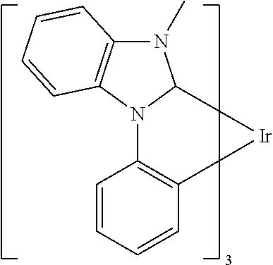
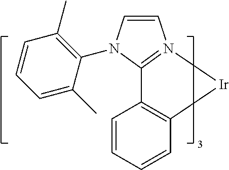
It has been reported in the art to introduce various heavy metal-containing sensitizers such as iridium and platinum complexes. Red to green, red to blue, and green to blue up-conversation have been achieved using different systems. Photon up-conversation using TTA has been demonstrated in both dilute solutions and solid films. For example, Castellano et al reported a TTA system with Pd(OEP), DPA and poly(EO-EPI). They have shown that selective green excitation (544 nm) of palladium(II) octaethylporphyrin (PdOEP) leads to triplet sensitization of 9,10-diphenylanthracene (DPA), eventually producing blue singlet DPA fluorescence (400-525 nm) in these films. The chemical structures of (a) PdOEP, (b) DPA, and (c) EO-EPI, are shown below.
Figure US09140428-20150922-C00006
A polyfluorene copolymer and heavy metal containing sensitizer for TTA up-conversation has been reported. See US20080103279. By introducing a condensed ring system in the polymer chain, TTA can be greatly enhanced and it is possible to use this system in a semiconductor device and obtain improved performance. See, US20080103279 and Kondakov et al., Triplet annihilation exceeding spin statistical limit in highly efficient fluorescent organic light-emitting diodes, J. Appl. Phys. 106, 124510 (2009).
A light emitting device using a semiconductor light emitting device based on inorganic rare earth metal compounds with an up-converting material disposed in the path of the emission from the semiconductor light emitting device has also been described in the art. See, U.S. Pat. No. 7,471,706. However, there are inherent limitations to the device and methods described, including poor efficiency of less than 10% due to several steps of energy transfer. Therefore, it may be difficult to achieve highly efficient displays with RGD up-converting systems. In addition, the inorganic rare earth metal device also requires a coherent light source, which further limits the usefulness of the device. See, Journal of Display Technology, 2, 68 (2006).
Embodiments of the prevent invention use triplet-triplet annihilation for up-conversation, and up to 60% efficiency has been reported for TTA-UC. See, J. Phys. Chem. Lett. 1, 1795 (2010). Therefore, TTA up-conversation may be more efficient than rare earth up-conversation system. In addition, a coherent light source is not required for TTA-UC. Furthermore, in the display architecture disclosed in embodiments of this invention, only the blue pixel was based on up-conversation, therefore the display may be reasonably efficient.
Although steady progress in the development of blue OLEDs has been made during the past two decades, the lifetime of blue devices still lags behind that of green and red OLEDs. Embodiments of the current invention provide a method of producing shorter wavelength emission from an OLED with longer wavelength emission. In particular, embodiments of the invention provide a method of producing blue light from a red or green OLED. This invention may overcome the problem of short lifetimes commonly seen in blue OLEDs. Additionally, embodiments of the invention provide an alternative to using less stable blue compounds in a device.
As disclosed herein, an OLED device is coupled with a solution or thin film, which contains compounds that can undergo TTA up-conversation. The OLED provides an excitation light source. The TTA media can absorb the light and convert it to shorter wavelength emission. For example, blue emission can be obtained by using a green OLED or red OLED with a TTA-UC layer. Long device operational lifetime can be achieved using these devices.
These devices using TTA-UC may have several applications. For example, it can be used to achieve cool white OLEDs, i.e., high correlated color temperature, using a warm white OLED, i.e., low correlated color temperature. The blue part of the spectrum can be generated from the TTA-UC. Furthermore, a white OLED can be obtained with a green/red OLED and a TTA-UC layer. It can also be used to generate monochrome blue light if a filter is used. The general concept is illustrated in FIG. 3, showing a cool white device 310, a white device 320 and a blue device 330. In one embodiment, a warm white OLED 300 and a TTA-UC layer 305 are stacked to form cool white device 310. In another embodiment, a green or red OLED 315 and a TTA-UC layer 305 are stacked to form white device 320. In a further embodiment, a green or red OLED 315, a TTA-UC layer 305 and a color filter 325 are stacked to form blue device 320.
Devices using triplet-triplet annihilation up conversation (TTA-UC) to covert emission from a light source, e.g., an OLED, to an emission with shorter wavelength are provided. A first device is provided, comprising a first organic light emitting device comprising a first material that is an emitting material having a first emissive spectrum, and a first triplet-triplet annihilation up-conversation layer disposed adjacent to the first organic light emitting device such that light emitted by the organic light emitting device is incident on the first up-conversation layer. The first triplet-triplet annihilation up-conversation layer comprising a first donor material and a first acceptor material, and the first donor material has an absorption spectrum that overlaps with the first emissive spectrum.
A variety of donor and acceptor materials may be suitable for use in these devices. Non-limiting examples of compounds that may be used in the up-conversation layer include those listed below in Table 1.
TABLE 1
λexcitation λemission
Donor Acceptor (nm) (nm) Reference
Figure US09140428-20150922-C00007
Figure US09140428-20150922-C00008
514.5 400 Chem. Comm. 2005, 3776-3777
Figure US09140428-20150922-C00009
Figure US09140428-20150922-C00010
442 360 J. Phys. Chem. A 2009, 113, 5912-5917
Figure US09140428-20150922-C00011
Figure US09140428-20150922-C00012
635 490 Inorg. Chem. 2009, 48, 2541-2548
Figure US09140428-20150922-C00013
Figure US09140428-20150922-C00014
544 445 J. Am. Chem. Soc. 2007, 129, 12652- 12653
Figure US09140428-20150922-C00015
Figure US09140428-20150922-C00016
725 560 J. Phys. Chem. A 2008, 112, 3550-3556
Figure US09140428-20150922-C00017
Figure US09140428-20150922-C00018
514.5 431 J. Phys. Chem. A 2008, 112, 3906-3910
Figure US09140428-20150922-C00019
Figure US09140428-20150922-C00020
450 390 J. Phys. Chem. A 2006, 110, 11440-11445
Figure US09140428-20150922-C00021
Figure US09140428-20150922-C00022
635 527 J. Am. Chem. Soc. 2008, 130, 16164- 16165
Figure US09140428-20150922-C00023
Figure US09140428-20150922-C00024
514.5 445 Chem. Comm. 2005, 3776-3777
Figure US09140428-20150922-C00025
Figure US09140428-20150922-C00026
635 556 J. Am. Chem. Soc. 2008, 130, 16164- 16165
Figure US09140428-20150922-C00027
Figure US09140428-20150922-C00028
695 500 Angew. Chem. Int. Ed. 2007, 46, 7693-7696
Figure US09140428-20150922-C00029
Figure US09140428-20150922-C00030
532 445 Chem. Commun. 2009, 4064- 4066
Figure US09140428-20150922-C00031
Figure US09140428-20150922-C00032
537 420 THE JOURNAL OF CHEMICAL PHYSICS 2005, 123, 074902
Figure US09140428-20150922-C00033
Figure US09140428-20150922-C00034
410 360 Journal of Luminescence 2009, 129, 303-306
Figure US09140428-20150922-C00035
Figure US09140428-20150922-C00036
700 560 J. Phys. Chem. Lett. 2010, 1, 1795-1799
Figure US09140428-20150922-C00037
Figure US09140428-20150922-C00038
635 445 J. Phys. Chem. Lett. 2010, 1, 195- 200
In one aspect, the device further comprises a pixel, which further comprises three subpixels (illustrated in FIG. 4). The first subpixel comprises the first organic light emitting device and the first up-conversation layer disposed adjacent to the first organic light emitting device. The second subpixel comprises a second organic light emitting device comprising a second material that is an emitting material having a second emissive spectrum. Preferably, the second subpixel does not include an up-conversation layer or a down conversion layer. The third subpixel comprises a third organic light emitting device comprising a third material that is an emitting material having a third emissive spectrum. For example, device 400 comprises three subpixels 405, 410 and 415, each of which emits a different color light. The first subpixel 405 comprises a green PHOLED 420 and an up-conversion layer 425. Green light emitted from the green PHOLED 420 is absorbed by the up-conversion layer 425, and emitted as blue light. The second subpixel 410 comprises a green PHOLED 420. Green light emitted from the green PHOLED 420 is not absorbed by an up-conversion layer or a down-conversion layer, resulting in green emission. The third subpixel 415 comprises a green PHOLED 420 and a down-conversion layer 430. Green light emitted from the green PHOLED 420 is absorbed by the down-conversion layer 430, and emitted as red light. Preferably, each of the green PHOLEDS 420 in subpixels 405, 410 and 415 are made from the same materials and have the same device structure, thereby allowing the device 400 having red, green and blue emission to be manufactured using the device architecture and materials of a single green PHOLED.
Device 500 also contains three subpixels 505, 510 and 515, each of which emits a different color light, but device 500 has a different device architecture than device 400. The first subpixel 505 comprises a green PHOLED 520 and an up-conversion layer 525. Green light emitted from the green PHOLED 520 is absorbed by the up-conversion layer 525, and emitted as blue light. The second subpixel 510 comprises a green PHOLED 520. Green light emitted from the green PHOLED 520 is not absorbed by an up-conversion layer or a down-conversion layer, resulting in green emission. The third subpixel 515 comprises a red PHOLED 530. Red light emitted from the red PHOLED 530 is not absorbed by an up-conversion layer or a down-conversion layer, resulting in red emission. Preferably, each of the green PHOLEDS 520 in subpixels 505 and 510 are made from the same materials and have the same device structure, thereby allowing the blue and green emission of device 500 to be manufactured using the device architecture and materials of a single green PHOLED.
In another aspect, the third subpixel further comprises a first down conversion layer disposed adjacent to the third organic light emitting device such that light emitted by the third organic light emitting device is incident on the first down conversion layer.
In yet another aspect, the first material, the second material, and the third material have an emissive spectrum having a peak wavelength of about 500 nm to about 600 nm. Preferably, the first material, the second material, and the third material are the same material.
In a further aspect, the first and the second materials have an emissive spectrum having a peak wavelength of about 500 nm to about 600 nm, and the third material has an emissive spectrum having a peak wavelength of about 600 nm to about 700 nm. Preferably, the second subpixel does not comprise an up-conversation layer or a down conversion layer.
In one aspect, the first subpixel has an emissive spectrum that has a peak wavelength of about 400 nm to about 500 nm, the second subpixel has an emissive spectrum that has a peak wavelength of about 500 nm to about 600 nm, and the third subpixel has an emissive spectrum that has a peak wavelength of about 600 nm to about 700 nm.
In another aspect, the first material, the second material, and the third material have an emissive spectrum having a peak wavelength of about 500 nm to about 600 nm. In the first subpixel, the first material emits light having a peak wavelength of about 500 to about 600 nm. The first up-conversation layer absorbs light having a peak wavelength of about 500 nm to about 600 nm and emits light having a peak wavelength of about 400 nm to about 500 nm, such that the first subpixel emits light having a peak wavelength of about 400 nm to about 500 nm. The second subpixel does not include an up-conversation or a down conversion layer, and the second material emits light having a peak wavelength of about 500 nm to about 600 nm, such that the second subpixel emits light having a wavelength of about 500 nm to about 600 nm. The third subpixel includes a down conversion layer, which absorbs light having a peak wavelength of about 500 nm to about 600 nm and emits light having a peak wavelength of about 600 nm to about 700 nm, such that the third subpixel emits light having a peak wavelength of about 600 nm to about 700 nm. Preferably, the first material, the second material, and the third material are the same material.
In one aspect, the first triplet-triplet annihilation up-conversation layer absorbs between about 80 percent and about 100 percent of the light emitted from the organic light emitting device.
In another aspect, the device further comprises at least one filter that absorbs light having a peak wavelength of about 500 nm to about 600 nm.
In yet another aspect, the device further comprises at least one microcavity that absorbs light having a peak wavelength of about 500 nm to about 600 nm.
In a further aspect, the device absorbs 99 percent of the emitted light emitted by the first material.
In one aspect, the organic light emitting device is capable of emitting a first spectrum of light having a first peak wavelength when voltage is applied to the device. The first triplet-triplet annihilation up-conversation layer is capable of absorbing the first spectrum of light and emitting a second spectrum of light with a second peak wavelength. The second peak wavelength is shorter than the first peak wavelength.
In another aspect, the first triplet-triplet annihilation up-conversation layer absorbs between about 20 percent and about 80 percent of the light emitted by the first material.
In one aspect, the device has CIE coordinates of x=0.10-0.40, y=0.05-0.40.
In another aspect, the device has a CRI of about 80 to about 100.
In one aspect, the first triplet-triplet annihilation up-conversation layer is a solution. In another aspect, the first triplet-triplet annihilation up-conversation layer is a solid film.
In one aspect, the light source is a green organic light emitting device or red organic light emitting device.
In another aspect, the first material emits light having CIE coordinates of within a seven step McAdam ellipse centered on the black body curve with a correlated color temperature (CCT) in the range of 2500-7400K and the first device emits light having CIE coordinates of within a seven step McAdam ellipse centered on the black body curve with a correlated color temperature (CCT) at least 50K higher than that of the emission of the first material.
In yet another aspect, the first material emits light having a peak wavelength of about 500 nm to about 700 nm, and the first device emits light having CIE coordinates of within a seven step McAdam ellipse centered on the black body curve with a correlated color temperature (CCT) in the range of 4000-7000K.
In one aspect, the first device further comprises a filter deposited over the organic light emitting device.
In one aspect, the first device is an area emitting device.
In one aspect, the first triplet-triplet annihilation up-conversation layer and the organic light emitting device are deposited on the same substrate. In another aspect, the first triplet-triplet annihilation up-conversation layer is vertically-stacked upon the organic light emitting device. In yet another aspect, the first triplet-triplet annihilation up-conversation layer and the organic light emitting device are positioned side by side.
In one aspect, the first device is a display. In another aspect, the first device is suitable for general illumination purposes.
In one aspect, the first triplet-triplet annihilation up-conversation layer has a linear or circular light polarization function.
In one aspect, the first material is a small molecule. In another aspect, the first material is a phosphorescent molecule.
In one aspect, up-conversation is achieved through triplet-triplet annihilation.
In one aspect, the first donor materials are selected from the group consisting of:
Figure US09140428-20150922-C00039
Figure US09140428-20150922-C00040
The first donor materials may be substituted or unsubstituted.
In another aspect, the first acceptor materials are selected from the group consisting of:
Figure US09140428-20150922-C00041
Figure US09140428-20150922-C00042
The first acceptor materials may be substituted or unsubstituted.
Methods of operating a device are also provided. The methods comprise driving an organic light emitting device to generate light, absorbing the light in a first up-conversation layer, shortening the wavelength of the light using triplet-triplet annihilation up-conversation, and emitting the light.
Combination with Other Materials
The materials described herein as useful for a particular layer in an organic light emitting device as incident light source for up-conversation may be used in combination with a wide variety of other materials present in the device. For example, emissive dopants disclosed herein may be used in conjunction with a wide variety of hosts, transport layers, blocking layers, injection layers, electrodes and other layers that may be present. The materials described or referred to below are non-limiting examples of materials that may be useful in combination with the compounds disclosed herein, and one of skill in the art can readily consult the literature to identify other materials that may be useful in combination.
HIL/HTL:
A hole injecting/transporting material to be used in embodiments of the present invention is not particularly limited, and any compound may be used as long as the compound is typically used as a hole injecting/transporting material. Examples of the material include, but are not limited to: a phthalocyanine or porphyrin derivative; an aromatic amine derivative; an indolocarbazole derivative; a polymer containing fluorohydrocarbon; a polymer with conductivity dopants; a conducting polymer, such as PEDOT/PSS; a self-assembly monomer derived from compounds such as phosphonic acid and silane derivatives; a metal oxide derivative, such as MoOx; a p-type semiconducting organic compound, such as 1,4,5,8,9,12-Hexaazatriphenylenehexacarbonitrile; a metal complex, and a cross-linkable compounds.
Examples of aromatic amine derivatives used in HIL or HTL include, but are not limited to the following general structures:
Figure US09140428-20150922-C00043
Each of Ar1 to Ar9 is selected from the group consisting aromatic hydrocarbon cyclic compounds such as benzene, biphenyl, triphenyl, triphenylene, naphthalene, anthracene, phenalene, phenanthrene, fluorene, pyrene, chrysene, perylene, azulene; group consisting aromatic heterocyclic compounds such as dibenzothiophene, dibenzofuran, dibenzoselenophene, furan, thiophene, benzofuran, benzothiophene, benzoselenophene, carbazole, indolocarbazole, pyridylindole, pyrrolodipyridine, pyrazole, imidazole, triazole, oxazole, thiazole, oxadiazole, oxatriazole, dioxazole, thiadiazole, pyridine, pyridazine, pyrimidine, pyrazine, triazine, oxazine, oxathiazine, oxadiazine, indole, benzimidazole, indazole, indoxazine, benzoxazole, benzisoxazole, benzothiazole, quinoline, isoquinoline, cinnoline, quinazoline, quinoxaline, naphthyridine, phthalazine, pteridine, xanthene, acridine, phenazine, phenothiazine, phenoxazine, benzofuropyridine, furodipyridine, benzothienopyridine, thienodipyridine, benzoselenophenopyridine, and selenophenodipyridine; and group consisting 2 to 10 cyclic structural units which are groups of the same type or different types selected from the aromatic hydrocarbon cyclic group and the aromatic heterocyclic group and are bonded to each other directly or via at least one of oxygen atom, nitrogen atom, sulfur atom, silicon atom, phosphorus atom, boron atom, chain structural unit and the aliphatic cyclic group. Wherein each Ar is further substituted by a substituent selected from the group consisting of hydrogen, alkyl, alkoxy, amino, alkenyl, alkynyl, arylalkyl, heteroalkyl, aryl and heteroaryl.
In one aspect, Ar1 to Ar9 is independently selected from the group consisting of:
Figure US09140428-20150922-C00044
k is an integer from 1 to 20; X1 to X8 is CH or N; Ar1 has the same group defined above.
Examples of metal complexes used in HIL or HTL include, but are not limited to the following general formula:
Figure US09140428-20150922-C00045
M is a metal, having an atomic weight greater than 40; (Y1-Y2) is a bidentate ligand, Y1 and Y2 are independently selected from C, N, O, P, and S; L is an ancillary ligand; m is an integer value from 1 to the maximum number of ligands that may be attached to the metal; and m+n is the maximum number of ligands that may be attached to the metal.
In one aspect, (Y1-Y2) is a 2-phenylpyridine derivative.
In another aspect, (Y1-Y2) is a carbene ligand.
In another aspect, M is selected from Ir, Pt, Os, and Zn.
In a further aspect, the metal complex has a smallest oxidation potential in solution vs. Fc+/Fc couple less than about 0.6 V.
Host:
The light emitting layer of the organic EL device in embodiments of the present invention preferably contains at least a metal complex as light emitting material, and may contain a host material using the metal complex as a dopant material. Examples of the host material are not particularly limited, and any metal complexes or organic compounds may be used as long as the triplet energy of the host is larger than that of the dopant.
Examples of metal complexes used as host are preferred to have the following general formula:
Figure US09140428-20150922-C00046
M is a metal; (Y3-Y4) is a bidentate ligand, Y3 and Y4 are independently selected from C, N, O, P, and S; L is an ancillary ligand; m is an integer value from 1 to the maximum number of ligands that may be attached to the metal; and m+n is the maximum number of ligands that may be attached to the metal.
In one aspect, the metal complexes are:
Figure US09140428-20150922-C00047
(O—N) is a bidentate ligand, having metal coordinated to atoms O and N.
In another aspect, M is selected from Ir and Pt.
In a further aspect, (Y3-Y4) is a carbene ligand.
Examples of organic compounds used as host are selected from the group consisting aromatic hydrocarbon cyclic compounds such as benzene, biphenyl, triphenyl, triphenylene, naphthalene, anthracene, phenalene, phenanthrene, fluorene, pyrene, chrysene, perylene, azulene; group consisting aromatic heterocyclic compounds such as dibenzothiophene, dibenzofuran, dibenzoselenophene, furan, thiophene, benzofuran, benzothiophene, benzoselenophene, carbazole, indolocarbazole, pyridylindole, pyrrolodipyridine, pyrazole, imidazole, triazole, oxazole, thiazole, oxadiazole, oxatriazole, dioxazole, thiadiazole, pyridine, pyridazine, pyrimidine, pyrazine, triazine, oxazine, oxathiazine, oxadiazine, indole, benzimidazole, indazole, indoxazine, benzoxazole, benzisoxazole, benzothiazole, quinoline, isoquinoline, cinnoline, quinazoline, quinoxaline, naphthyridine, phthalazine, pteridine, xanthene, acridine, phenazine, phenothiazine, phenoxazine, benzofuropyridine, furodipyridine, benzothienopyridine, thienodipyridine, benzoselenophenopyridine, and selenophenodipyridine; and group consisting 2 to 10 cyclic structural units which are groups of the same type or different types selected from the aromatic hydrocarbon cyclic group and the aromatic heterocyclic group and are bonded to each other directly or via at least one of oxygen atom, nitrogen atom, sulfur atom, silicon atom, phosphorus atom, boron atom, chain structural unit and the aliphatic cyclic group. Wherein each group is further substituted by a substituent selected from the group consisting of hydrogen, alkyl, alkoxy, amino, alkenyl, alkynyl, arylalkyl, heteroalkyl, aryl and heteroaryl.
In one aspect, host compound contains at least one of the following groups in the molecule:
Figure US09140428-20150922-C00048
R1 to R7 is independently selected from the group consisting of hydrogen, alkyl, alkoxy, amino, alkenyl, alkynyl, arylalkyl, heteroalkyl, aryl and heteroaryl, when it is aryl or heteroaryl, it has the similar definition as Ar's mentioned above.
k is an integer from 0 to 20.
X1 to X8 is selected from CH or N.
HBL:
A hole blocking layer (HBL) may be used to reduce the number of holes and/or excitons that leave the emissive layer. The presence of such a blocking layer in a device may result in substantially higher efficiencies as compared to a similar device lacking a blocking layer. Also, a blocking layer may be used to confine emission to a desired region of an OLED.
In one aspect, compound used in HBL contains the same molecule used as host described above.
In another aspect, compound used in HBL contains at least one of the following groups in the molecule:
Figure US09140428-20150922-C00049
k is an integer from 0 to 20; L is an ancillary ligand, m is an integer from 1 to 3.
ETL:
Electron transport layer (ETL) may include a material capable of transporting electrons. Electron transport layer may be intrinsic (undoped), or doped. Doping may be used to enhance conductivity. Examples of the ETL material are not particularly limited, and any metal complexes or organic compounds may be used as long as they are typically used to transport electrons.
In one aspect, compound used in ETL contains at least one of the following groups in the molecule:
Figure US09140428-20150922-C00050
R1 is selected from the group consisting of hydrogen, alkyl, alkoxy, amino, alkenyl, alkynyl, arylalkyl, heteroalkyl, aryl and heteroaryl, when it is aryl or heteroaryl, it has the similar definition as Ar's mentioned above.
Ar1 to Ar3 has the similar definition as Ar's mentioned above.
k is an integer from 0 to 20.
X1 to X8 is selected from CH or N.
In another aspect, the metal complexes used in ETL contains, but are not limited to the following general formula:
Figure US09140428-20150922-C00051
(O—N) or (N—N) is a bidentate ligand, having metal coordinated to atoms O, N or N, N; L is an ancillary ligand; m is an integer value from 1 to the maximum number of ligands that may be attached to the metal.
In any of the above-mentioned compounds used in each layer of OLED device, the hydrogen atoms can be partially or fully deuterated.
In addition to and/or in combination with the materials disclosed herein, many hole injection materials, hole transporting materials, host materials, dopant materials, exciton/hole blocking layer materials, electron transporting and electron injecting materials may be used in an OLED. Non-limiting examples of the materials that may be used in an OLED in combination with materials disclosed herein are listed in Table 2 below. Table 2 lists non-limiting classes of materials, non-limiting examples of compounds for each class, and references that disclose the materials.
TABLE 2
MATERIAL EXAMPLES OF MATERIAL PUBLICATIONS
Hole injection materials
Phthalocyanine and porphryin compounds
Figure US09140428-20150922-C00052
Appl. Phys. Lett. 69, 2160 (1996)
Starburst triarylamines
Figure US09140428-20150922-C00053
J. Lumin. 72-74, 985 (1997)
CFx Fluoro- hydrocarbon polymer
Figure US09140428-20150922-C00054
Appl. Phys. Lett. 78, 673 (2001)
Conducting polymers (e.g., PEDOT:PSS, polyaniline, polypthiophene)
Figure US09140428-20150922-C00055
Synth. Met. 87, 171 (1997) WO2007002683
Phosphonic acid and sliane SAMs
Figure US09140428-20150922-C00056
US20030162053
Triarylamine or polythiophene polymers with conductivity dopants
Figure US09140428-20150922-C00057
EA01725079A1
and
Figure US09140428-20150922-C00058
Figure US09140428-20150922-C00059
Arylamines complexed with metal oxides such as molybdenum and tungsten oxides
Figure US09140428-20150922-C00060
SID Symposium Digest, 37, 923 (2006) WO2009018009
p-type semiconducting organic complexes
Figure US09140428-20150922-C00061
US20020158242
Metal organometallic complexes
Figure US09140428-20150922-C00062
US20060240279
Cross-linkable compounds
Figure US09140428-20150922-C00063
US20080220265
Hole transporting materials
Triarylamines (e.g., TPD, α-NPD)
Figure US09140428-20150922-C00064
Appl. Phys. Lett. 51, 913 (1987)
Figure US09140428-20150922-C00065
U.S. Pat. No. 5,061,569
Figure US09140428-20150922-C00066
EP650955
Figure US09140428-20150922-C00067
J. Mater. Chem. 3, 319 (1993)
Figure US09140428-20150922-C00068
Appl. Phys. Lett. 90, 183503 (2007)
Figure US09140428-20150922-C00069
Appl. Phys. Lett. 90, 183503 (2007)
Triaylamine on spirofluorene core
Figure US09140428-20150922-C00070
Synth. Met. 91, 209 (1997)
Arylamine carbazole compounds
Figure US09140428-20150922-C00071
Adv. Mater. 6, 677 (1994), US20080124572
Triarylamine with (di)benzothiophene/ (di)benzofuran
Figure US09140428-20150922-C00072
US20070278938, US20080106190
Indolocarbazoles
Figure US09140428-20150922-C00073
Synth. Met. 111, 421 (2000)
Isoindole compounds
Figure US09140428-20150922-C00074
Chem. Mater. 15, 3148 (2003)
Metal carbene complexes
Figure US09140428-20150922-C00075
US20080018221
Phosphorescent OLED host materials
Red hosts
Arylcarbazoles
Figure US09140428-20150922-C00076
Appl. Phys. Lett. 78, 1622 (2001)
Metal 8- hydroxyquinolates (e.g., Alq3, BAlq)
Figure US09140428-20150922-C00077
Nature 395, 151 (1998)
Figure US09140428-20150922-C00078
US20060202194
Figure US09140428-20150922-C00079
WO2005014551
Figure US09140428-20150922-C00080
WO2006072002
Metal phenoxy- benzothiazole compounds
Figure US09140428-20150922-C00081
Appl. Phys. Lett. 90, 123509 (2007)
Conjugated oligomers and polymers (e.g., polyfluorene)
Figure US09140428-20150922-C00082
Org. Electron. 1, 15 (2000)
Aromatic fused rings
Figure US09140428-20150922-C00083
WO2009066779, WO2009066778, WO2009063833, US20090045731, US20090045730, WO2009008311, US20090008605, US20090009065
Zinc complexes
Figure US09140428-20150922-C00084
WO2009062578
Green hosts
Arylcarbazoles
Figure US09140428-20150922-C00085
Appl. Phys. Lett. 78, 1622 (2001)
Figure US09140428-20150922-C00086
US20030175553
Figure US09140428-20150922-C00087
WO2001039234
Aryltriphenylene compounds
Figure US09140428-20150922-C00088
US20060280965
Figure US09140428-20150922-C00089
US20060280965
Figure US09140428-20150922-C00090
WO2009021126
Donor acceptor type molecules
Figure US09140428-20150922-C00091
WO2008056746
Aza-carbazole/ DBT/DBF
Figure US09140428-20150922-C00092
JP2008074939
Polymers (e.g., PVK)
Figure US09140428-20150922-C00093
Appl. Phys. Lett. 77, 2280 (2000)
Spirofluorene compounds
Figure US09140428-20150922-C00094
WO2004093207
Metal phenoxy- benzooxazole compounds
Figure US09140428-20150922-C00095
WO2005089025
Figure US09140428-20150922-C00096
WO2006132173
Figure US09140428-20150922-C00097
JP200511610
Spirofluorene- carbazole compounds
Figure US09140428-20150922-C00098
JP2007254297
Figure US09140428-20150922-C00099
JP2007254297
Indolocabazoles
Figure US09140428-20150922-C00100
WO2007063796
Figure US09140428-20150922-C00101
WO2007063754
5-member ring electron deficient heterocycles (e.g., triazole, oxadiazole)
Figure US09140428-20150922-C00102
J. Appl. Phys. 90, 5048 (2001)
Figure US09140428-20150922-C00103
WO2004107822
Tetraphenylene complexes
Figure US09140428-20150922-C00104
US20050112407
Metal phenoxypyridine compounds
Figure US09140428-20150922-C00105
WO2005030900
Metal coordination complexes (e.g., Zn, Al with N{circumflex over ( )}N ligands)
Figure US09140428-20150922-C00106
US20040137268, US20040137267
Blue hosts
Arylcarbazoles
Figure US09140428-20150922-C00107
Appl. Phys. Lett, 82, 2422 (2003)
Figure US09140428-20150922-C00108
US20070190359
Dibenzothiophene/ Dibenzofuran- carbazole compounds
Figure US09140428-20150922-C00109
WO2006114966, US20090167162
Figure US09140428-20150922-C00110
US20090167162
Figure US09140428-20150922-C00111
WO2009086028
Figure US09140428-20150922-C00112
US20090030202, US20090017330
Silicon aryl compounds
Figure US09140428-20150922-C00113
US20050238919
Figure US09140428-20150922-C00114
WO2009003898
Silicon/ Germanium aryl compounds
Figure US09140428-20150922-C00115
EP2034538A
Aryl benzoyl ester
Figure US09140428-20150922-C00116
WO2006100298
High triplet metal organometallic complex
Figure US09140428-20150922-C00117
U.S. Pat. No. 7,154,114
Phosphorescent dopants
Red dopants
Heavy metal porphyrins (e.g., PtOEP)
Figure US09140428-20150922-C00118
Nature 395, 151 (1998)
Iridium(III) organometallic complexes
Figure US09140428-20150922-C00119
Appl. Phys. Lett. 78, 1622 (2001)
Figure US09140428-20150922-C00120
US2006835469
Figure US09140428-20150922-C00121
US2006835469
Figure US09140428-20150922-C00122
US20060202194
Figure US09140428-20150922-C00123
US20060202194
Figure US09140428-20150922-C00124
US20070087321
Figure US09140428-20150922-C00125
US20070087321
Figure US09140428-20150922-C00126
Adv. Mater. 19, 739 (2007)
Figure US09140428-20150922-C00127
WO2009100991
Figure US09140428-20150922-C00128
WO2008101842
Platinum(II) organometallic complexes
Figure US09140428-20150922-C00129
WO2003040257
Osminum(III) complexes
Figure US09140428-20150922-C00130
Chem. Mater. 17, 3532 (2005)
Ruthenium(II) complexes
Figure US09140428-20150922-C00131
Adv. Mater. 17, 1059 (2005)
Rhenium (I), (II), and (III) complexes
Figure US09140428-20150922-C00132
US20050244673
Green dopants
Iridium(III) organometallic complexes
Figure US09140428-20150922-C00133
Inorg. Chem. 40, 1704 (2001)
Figure US09140428-20150922-C00134
US20020034656
Figure US09140428-20150922-C00135
U.S. Pat. No. 7,332,232
Figure US09140428-20150922-C00136
US20090108737
Figure US09140428-20150922-C00137
US20090039776
Figure US09140428-20150922-C00138
U.S. Pat. No. 6,921,915
Figure US09140428-20150922-C00139
U.S. Pat. No. 6,687,266
Figure US09140428-20150922-C00140
Chem. Mater. 16, 2480 (2004)
Figure US09140428-20150922-C00141
US20070190359
Figure US09140428-20150922-C00142
US 20060008670 JP2007123392
Figure US09140428-20150922-C00143
Adv. Mater. 16, 2003 (2004)
Figure US09140428-20150922-C00144
Angew. Chem. Int. Ed. 2006, 45, 7800
Figure US09140428-20150922-C00145
WO2009050290
Figure US09140428-20150922-C00146
US20090165846
Figure US09140428-20150922-C00147
US20080015355
Monomer for polymeric metal organometallic compounds
Figure US09140428-20150922-C00148
U.S. Pat. No. 7,250,226, U.S. Pat. No. 7,396,598
Pt(II) organometallic complexes, including polydentated ligands
Figure US09140428-20150922-C00149
Appl. Phys. Lett. 86, 153505 (2005)
Figure US09140428-20150922-C00150
Appl. Phys. Lett. 86, 153505 (2005)
Figure US09140428-20150922-C00151
Chem. Lett. 34, 592 (2005)
Figure US09140428-20150922-C00152
WO2002015645
Figure US09140428-20150922-C00153
US20060263635
Cu complexes
Figure US09140428-20150922-C00154
WO2009000673
Gold complexes
Figure US09140428-20150922-C00155
Chem. Commun. 2906 (2005)
Rhenium(III) complexes
Figure US09140428-20150922-C00156
Inorg. Chem. 42, 1248 (2003)
Deuterated organometallic complexes
Figure US09140428-20150922-C00157
US20030138657
Organometallic complexes with two or more metal centers
Figure US09140428-20150922-C00158
US20030152802
Figure US09140428-20150922-C00159
U.S. Pat. No. 7,090,928
Blue dopants
Iridium(III) organometallic complexes
Figure US09140428-20150922-C00160
WO2002002714
Figure US09140428-20150922-C00161
WO2006009024
Figure US09140428-20150922-C00162
US20060251923
Figure US09140428-20150922-C00163
U.S. Pat. No. 7,393,599, WO2006056418, US20050260441, WO2005019373
Figure US09140428-20150922-C00164
U.S. Pat. No. 7,534,505
Figure US09140428-20150922-C00165
U.S. Pat. No. 7,445,855
Figure US09140428-20150922-C00166
US20070190359, US20080297033
Figure US09140428-20150922-C00167
U.S. Pat. No. 7,338,722
Figure US09140428-20150922-C00168
US20020134984
Figure US09140428-20150922-C00169
Angew. Chem. Int. Ed. 47, 1 (2008)
Figure US09140428-20150922-C00170
Chem. Mater. 18, 5119 (2006)
Figure US09140428-20150922-C00171
Inorg. Chem. 46, 4308 (2007)
Figure US09140428-20150922-C00172
WO2005123873
Figure US09140428-20150922-C00173
WO2005123873
Figure US09140428-20150922-C00174
WO2007004380
Figure US09140428-20150922-C00175
WO2006082742
Osmium(II) complexes
Figure US09140428-20150922-C00176
U.S. Pat. No. 7,279,704
Figure US09140428-20150922-C00177
Organometallics 23, 3745 (2004)
Gold complexes
Figure US09140428-20150922-C00178
Appl. Phys. Lett. 74, 1361 (1999)
Platinum(II) complexes
Figure US09140428-20150922-C00179
WO2006098120, WO2006103874
Exciton/hole blocking layer materials
Bathocuprine compounds (e.g., BCP, BPhen)
Figure US09140428-20150922-C00180
Appl. Phys. Lett. 75, 4 (1999)
Figure US09140428-20150922-C00181
Appl. Phys. Lett. 79, 449 (2001)
Metal 8- hydroxy- quinolates (e.g., BAlq)
Figure US09140428-20150922-C00182
Appl. Phys. Lett. 81, 162 (2002)
5-member ring electron deficient heterocycles such as triazole, oxadiazole, imidazole, benzoimidazole
Figure US09140428-20150922-C00183
Appl. Phys. Lett. 81, 162 (2002)
Triphenylene compounds
Figure US09140428-20150922-C00184
US20050025993
Fluorinated aromatic compounds
Figure US09140428-20150922-C00185
Appl. Phys. Lett. 79, 156 (2001)
Phenothiazine- S-oxide
Figure US09140428-20150922-C00186
WO2008132085
Electron transporting materials
Anthracene- benzoimidazole compounds
Figure US09140428-20150922-C00187
WO2003060956
Figure US09140428-20150922-C00188
US20090179554
Aza triphenylene derivatives
Figure US09140428-20150922-C00189
US20090115316
Anthracene- benzothiazole compounds
Figure US09140428-20150922-C00190
Appl. Phys. Lett. 89, 063504 (2006)
Metal 8- hydroxy- quinolates (e.g., Alq3, Zrq4)
Figure US09140428-20150922-C00191
Appl. Phys. Lett. 51, 913 (1987) U.S. Pat. No. 7,230,107
Metal hydroxy- benoquinolates
Figure US09140428-20150922-C00192
Chem. Lett. 5, 905 (1993)
Bathocuprine compounds such as BCP, BPhen, etc
Figure US09140428-20150922-C00193
Appl. Phys. Lett. 91, 263503 (2007)
Figure US09140428-20150922-C00194
Appl. Phys. Lett. 79, 449 (2001)
5-member ring electron deficient heterocycles (e.g., triazole, oxadiazole, imidazole, benzoimidazole)
Figure US09140428-20150922-C00195
Appl. Phys. Lett. 74, 865 (1999)
Figure US09140428-20150922-C00196
Appl. Phys. Lett. 55, 1489 (1989)
Figure US09140428-20150922-C00197
Jpn. J. Apply. Phys. 32, L917 (1993)
Silole compounds
Figure US09140428-20150922-C00198
Org. Electron. 4, 113 (2003)
Arylborane compounds
Figure US09140428-20150922-C00199
J. Am. Chem. Soc. 120, 9714 (1998)
Fluorinated aromatic compounds
Figure US09140428-20150922-C00200
J. Am. Chem. Soc. 122, 1832 (2000)
Fullerene (e.g., C60)
Figure US09140428-20150922-C00201
US20090101870
Triazine complexes
Figure US09140428-20150922-C00202
US20040036077
Zn (N{circumflex over ( )}N) complexes
Figure US09140428-20150922-C00203
U.S. Pat. No. 6,528,187
It is understood that the various embodiments described herein are by way of example only, and are not intended to limit the scope of the invention. For example, many of the materials and structures described herein may be substituted with other materials and structures without deviating from the spirit of the invention. The present invention as claimed may therefore includes variations from the particular examples and preferred embodiments described herein, as will be apparent to one of skill in the art. It is understood that various theories as to why the invention works are not intended to be limiting.

Claims (16)

The invention claimed is:
1. A method of operating a device, comprising:
driving a first organic light emitting device within a first subpixel of a pixel to generate light, the first organic light emitting device comprising a first material that is an emissive material having a first emissive spectrum, the light generated by the first organic light emitting device being absorbed by a first triplet-triplet annihilation up-conversation layer in the pixel, the first triplet-triplet annihilation up-conversion layer comprising a first donor material and a first acceptor material, the first donor material having an absorption spectrum that overlaps with the first emissive spectrum, the generated light causing the wavelength of the light to be shortened via triplet-triplet annihilation up-conversation and emitted by the pixel;
driving a second organic light emitting device in a second subpixel of the pixel, the second organic light emitting device comprising a second material that is an emitting material having a second emissive spectrum with a peak wavelength of about 500 nm to about 600 nm; and
driving a third organic light emitting device in a third subpixel of the pixel, the third, organic light emitting device comprising a third material that is an emitting material having a third emissive spectrum with a peak wavelength of about 600 nm to about 700 nm.
2. The method of claim 1, fin her comprising:
absorbing the light generated by the second organic light emitting device in a first down conversion layer to lengthen the light generated by the second organic light emitting device; and
emitting the light generated by the second organic light emitting device having a lengthened wavelength.
3. The method of claim 1, wherein the step of driving the first organic light emitting device to generate light comprises driving the first organic light emitting device to generate light having a peak wavelength of about 500 to about 600 nm.
4. The method of claim 1, further comprising absorbing at least a portion of light generated by the first organic light emitting device with a filter.
5. The method of claim 1, further comprising absorbing at least a portion of light generated by the first organic light emitting device with a microcavity.
6. The method of claim 1, wherein the step of absorbing the light in the first triplet triplet annihilation up-conversion layer comprises absorbing between about 80% and about 100% of light emitted from the first organic light emitting device.
7. The method of claim 1, wherein the first triplet-triplet annihilation up-conversion layer is a solution.
8. The method of claim 1, wherein the first triplet-triplet annihilation up-conversion layer is a solid film.
9. The method of claim 1, wherein the first triplet-triplet annihilation up-conversation layer has a linear or circular light polarization function.
10. The method of claim 1, wherein the first organic light emitting device comprises a first emissive material that comprises a small molecule.
11. The method of claim 1, wherein the first organic light emitting device comprises a first emissive material that comprises a phosphorescent molecule.
12. The method of claim 1, wherein the first organic light emitting device is a green organic light emitting device or red organic light emitting device.
13. The method of claim 1, wherein the first donor material is selected from the group consisting of
Figure US09140428-20150922-C00204
Figure US09140428-20150922-C00205
wherein the first donor material may be substituted or unsubstituted; and
wherein the first acceptor material is selected from the group consisting of:
Figure US09140428-20150922-C00206
Figure US09140428-20150922-C00207
wherein the first acceptor material may be substituted or unsubstituted.
14. The method of claim 1, wherein the first triplet-triplet annihilation up-conversation layer and the organic light emitting device are disposed on the same substrate.
15. The method of claim 1, wherein the first triplet-triplet annihilation up-conversation layer is vertically-stacked upon the organic light emitting device.
16. The method of claim 1, wherein the first triplet-triplet annihilation up-conversation layer and the organic light emitting device are positioned side by side.
US14/256,007 2010-06-11 2014-04-18 Triplet-triplet annihilation up-conversation for display and lighting applications Active US9140428B2 (en)

Priority Applications (1)

Application Number Priority Date Filing Date Title
US14/256,007 US9140428B2 (en) 2010-06-11 2014-04-18 Triplet-triplet annihilation up-conversation for display and lighting applications

Applications Claiming Priority (3)

Application Number Priority Date Filing Date Title
US39754210P 2010-06-11 2010-06-11
US12/901,901 US8742657B2 (en) 2010-06-11 2010-10-11 Triplet-Triplet annihilation up conversion (TTA-UC) for display and lighting applications
US14/256,007 US9140428B2 (en) 2010-06-11 2014-04-18 Triplet-triplet annihilation up-conversation for display and lighting applications

Related Parent Applications (1)

Application Number Title Priority Date Filing Date
US12/901,901 Division US8742657B2 (en) 2010-06-11 2010-10-11 Triplet-Triplet annihilation up conversion (TTA-UC) for display and lighting applications

Publications (2)

Publication Number Publication Date
US20140226338A1 US20140226338A1 (en) 2014-08-14
US9140428B2 true US9140428B2 (en) 2015-09-22

Family

ID=44513109

Family Applications (2)

Application Number Title Priority Date Filing Date
US12/901,901 Active 2031-08-02 US8742657B2 (en) 2010-06-11 2010-10-11 Triplet-Triplet annihilation up conversion (TTA-UC) for display and lighting applications
US14/256,007 Active US9140428B2 (en) 2010-06-11 2014-04-18 Triplet-triplet annihilation up-conversation for display and lighting applications

Family Applications Before (1)

Application Number Title Priority Date Filing Date
US12/901,901 Active 2031-08-02 US8742657B2 (en) 2010-06-11 2010-10-11 Triplet-Triplet annihilation up conversion (TTA-UC) for display and lighting applications

Country Status (2)

Country Link
US (2) US8742657B2 (en)
WO (1) WO2011156793A1 (en)

Cited By (1)

* Cited by examiner, † Cited by third party
Publication number Priority date Publication date Assignee Title
US10622576B2 (en) 2016-11-30 2020-04-14 Industrial Technology Research Institute Organic light-emitting diode and white organic light-emitting diode

Families Citing this family (25)

* Cited by examiner, † Cited by third party
Publication number Priority date Publication date Assignee Title
WO2014030666A1 (en) 2012-08-24 2014-02-27 コニカミノルタ株式会社 Transparent electrode, electronic device, and method for manufacturing transparent electrode
US9196860B2 (en) 2012-12-04 2015-11-24 Universal Display Corporation Compounds for triplet-triplet annihilation upconversion
JP6314599B2 (en) 2013-03-29 2018-04-25 コニカミノルタ株式会社 COMPOUND FOR ORGANIC ELECTROLUMINESCENCE, ORGANIC ELECTROLUMINESCENCE ELEMENT, LIGHTING DEVICE AND DISPLAY DEVICE HAVING THE SAME
WO2014157494A1 (en) 2013-03-29 2014-10-02 コニカミノルタ株式会社 Material for organic electroluminescent elements, organic electroluminescent element, display device and lighting device
US9835731B2 (en) * 2013-12-11 2017-12-05 Halliburton Energy Services, Inc. Detector packages
CN105940083B (en) * 2014-01-31 2019-06-11 日本化药株式会社 Light wavelength conversion element containing ionic liquid and the article comprising the light wavelength conversion element
TWI577008B (en) * 2014-05-28 2017-04-01 友達光電股份有限公司 Display panel
CN105590945A (en) * 2014-11-17 2016-05-18 北京维信诺科技有限公司 Organic light-emitting display device containing quantum dots, display method and application thereof
CN105679959A (en) * 2014-11-17 2016-06-15 北京维信诺科技有限公司 Organic light-emitting display device
JP5831654B1 (en) 2015-02-13 2015-12-09 コニカミノルタ株式会社 Aromatic heterocycle derivative, organic electroluminescence device using the same, illumination device and display device
KR102382005B1 (en) * 2015-05-13 2022-04-01 삼성디스플레이 주식회사 Organic light emitting diode display
JP6728603B2 (en) 2015-09-08 2020-07-22 コニカミノルタ株式会社 Organic electroluminescence element and vehicle lamp
CN105280686B (en) 2015-10-23 2018-09-11 京东方科技集团股份有限公司 A kind of display panel and display device
JP6788314B2 (en) 2016-01-06 2020-11-25 コニカミノルタ株式会社 Organic electroluminescence element, manufacturing method of organic electroluminescence element, display device and lighting device
US10693096B2 (en) * 2016-03-18 2020-06-23 Sharp Kabushiki Kaisha EL element and method for manufacturing EL element with a light-emitting layer including an ionic liquid, a phosphorescent material, and a fluorescent material
US10665803B2 (en) * 2016-04-22 2020-05-26 The Trusteees Of Princeton University Solid-state organic intermediate-band photovoltaic devices
CN106784209A (en) * 2016-11-21 2017-05-31 武汉华星光电技术有限公司 A kind of full-color QLED display devices and preparation method thereof
CN108336119B (en) * 2018-03-20 2022-04-15 京东方科技集团股份有限公司 Pixel unit, pixel structure and display panel
CN108417727B (en) * 2018-04-04 2020-01-07 京东方科技集团股份有限公司 OLED light-emitting device, preparation method thereof and display device
KR20200002053A (en) * 2018-06-28 2020-01-08 삼성디스플레이 주식회사 Cyclometallic compound, organic light emitting device comprising the same and apparatus comprising the organic light emitting device
CN109037461B (en) * 2018-07-13 2021-12-14 京东方科技集团股份有限公司 Blue-light organic light-emitting diode, display substrate and display device
TWI708827B (en) * 2019-01-11 2020-11-01 元智大學 Organic light-emitting diode
CN110071222B (en) * 2019-04-25 2021-04-23 京东方科技集团股份有限公司 Light-emitting device, display panel and display device
KR20200129210A (en) * 2019-05-07 2020-11-18 삼성디스플레이 주식회사 Display device
CN111450421A (en) * 2020-04-10 2020-07-28 北京夏禾科技有限公司 Wearable phototherapy device

Citations (138)

* Cited by examiner, † Cited by third party
Publication number Priority date Publication date Assignee Title
US4769292A (en) 1987-03-02 1988-09-06 Eastman Kodak Company Electroluminescent device with modified thin film luminescent zone
US5061569A (en) 1990-07-26 1991-10-29 Eastman Kodak Company Electroluminescent device with organic electroluminescent medium
US5247190A (en) 1989-04-20 1993-09-21 Cambridge Research And Innovation Limited Electroluminescent devices
EP0650955A1 (en) 1993-11-01 1995-05-03 Hodogaya Chemical Co., Ltd. Amine compound and electro-luminescence device comprising same
US5541012A (en) 1992-05-08 1996-07-30 Nippon Telegraph And Telephone Corporation Infrared-to-visible up-conversion material
US5703436A (en) 1994-12-13 1997-12-30 The Trustees Of Princeton University Transparent contacts for organic devices
US5707745A (en) 1994-12-13 1998-01-13 The Trustees Of Princeton University Multicolor organic light emitting devices
US5834893A (en) 1996-12-23 1998-11-10 The Trustees Of Princeton University High efficiency organic light emitting devices with light directing structures
US5844363A (en) 1997-01-23 1998-12-01 The Trustees Of Princeton Univ. Vacuum deposited, non-polymeric flexible organic light emitting devices
US5912257A (en) 1995-09-06 1999-06-15 The Research Foundation Of State University Of New York Two-photon upconverting dyes and applications
US6013982A (en) 1996-12-23 2000-01-11 The Trustees Of Princeton University Multicolor display devices
US6087196A (en) 1998-01-30 2000-07-11 The Trustees Of Princeton University Fabrication of organic semiconductor devices using ink jet printing
US6091195A (en) 1997-02-03 2000-07-18 The Trustees Of Princeton University Displays having mesa pixel configuration
US6097147A (en) 1998-09-14 2000-08-01 The Trustees Of Princeton University Structure for high efficiency electroluminescent device
US6294398B1 (en) 1999-11-23 2001-09-25 The Trustees Of Princeton University Method for patterning devices
US6303238B1 (en) 1997-12-01 2001-10-16 The Trustees Of Princeton University OLEDs doped with phosphorescent compounds
WO2001039234A3 (en) 1999-11-24 2001-11-08 Univ Princeton Organic light emitting diode having a blue phosphorescent molecule as an emitter
US6337102B1 (en) 1997-11-17 2002-01-08 The Trustees Of Princeton University Low pressure vapor phase deposition of organic thin films
WO2002002714A2 (en) 2000-06-30 2002-01-10 E.I. Du Pont De Nemours And Company Electroluminescent iridium compounds with fluorinated phenylpyridines, phenylpyrimidines, and phenylquinolines and devices made with such compounds
WO2002015645A1 (en) 2000-08-11 2002-02-21 The Trustees Of Princeton University Organometallic compounds and emission-shifting organic electrophosphorescence
US20020034656A1 (en) 1998-09-14 2002-03-21 Thompson Mark E. Organometallic complexes as phosphorescent emitters in organic LEDs
US20020074935A1 (en) 2000-12-15 2002-06-20 Kwong Raymond C. Highly stable and efficient OLEDs with a phosphorescent-doped mixed layer architecture
US20020134984A1 (en) 2001-02-01 2002-09-26 Fuji Photo Film Co., Ltd. Transition metal complex and light-emitting device
US20020158242A1 (en) 1999-12-31 2002-10-31 Se-Hwan Son Electronic device comprising organic compound having p-type semiconducting characteristics
US6528187B1 (en) 1998-09-08 2003-03-04 Fuji Photo Film Co., Ltd. Material for luminescence element and luminescence element using the same
WO2003040257A1 (en) 2001-11-07 2003-05-15 E. I. Du Pont De Nemours And Company Electroluminescent platinum compounds and devices made with such compounds
US20030138657A1 (en) 2000-12-07 2003-07-24 Canon Kabushiki Kaisha Deuterated semi-conducting organic compounds used for opto-electronic devices
US20030152802A1 (en) 2001-06-19 2003-08-14 Akira Tsuboyama Metal coordination compound and organic liminescence device
US20030162053A1 (en) 1996-06-25 2003-08-28 Marks Tobin J. Organic light - emitting diodes and methods for assembly and enhanced charge injection
US20030175553A1 (en) 2001-12-28 2003-09-18 Thompson Mark E. White light emitting oleds from combined monomer and aggregate emission
WO2003060956A3 (en) 2002-01-18 2003-11-13 Lg Chemical Ltd New material for transporting electrons and organic electroluminescent display using the same
US6653778B1 (en) 1999-09-24 2003-11-25 Fuji Electric Co., Ltd. Fluorescent color conversion film, fluorescent color conversion filter using the conversion film, and organic light-emitting device equipped with the conversion filter
US20030230980A1 (en) 2002-06-18 2003-12-18 Forrest Stephen R Very low voltage, high efficiency phosphorescent oled in a p-i-n structure
US6687266B1 (en) 2002-11-08 2004-02-03 Universal Display Corporation Organic light emitting materials and devices
US20040036077A1 (en) 2002-08-22 2004-02-26 Fuji Photo Film Co., Ltd. Light emitting element
US6699406B2 (en) 1999-03-19 2004-03-02 Rutgers, The State University Rare earth doped host materials
US20040137268A1 (en) 2002-12-27 2004-07-15 Fuji Photo Film Co., Ltd. Organic electroluminescent device
US20040137267A1 (en) 2002-12-27 2004-07-15 Fuji Photo Film Co., Ltd. Organic electroluminescent device
US20040140758A1 (en) 2003-01-17 2004-07-22 Eastman Kodak Company Organic light emitting device (OLED) display with improved light emission using a metallic anode
US20040174116A1 (en) 2001-08-20 2004-09-09 Lu Min-Hao Michael Transparent electrodes
WO2004093207A2 (en) 2003-04-15 2004-10-28 Covion Organic Semiconductors Gmbh Mixtures of matrix materials and organic semiconductors capable of emission, use of the same and electronic components containing said mixtures
WO2004107822A1 (en) 2003-05-29 2004-12-09 Nippon Steel Chemical Co., Ltd. Organic electroluminescent element
US6835469B2 (en) 2001-10-17 2004-12-28 The University Of Southern California Phosphorescent compounds and devices comprising the same
JP2005011610A (en) 2003-06-18 2005-01-13 Nippon Steel Chem Co Ltd Organic electroluminescent element
US6844387B2 (en) 1998-11-25 2005-01-18 University Of Central Florida Composites of inorganic luminophores stabilized in polymer hosts
US20050025993A1 (en) 2003-07-25 2005-02-03 Thompson Mark E. Materials and structures for enhancing the performance of organic light emitting devices
WO2005014551A1 (en) 2003-08-07 2005-02-17 Nippon Steel Chemical Co., Ltd. Aluminum chelate compelx for organic el material
WO2005019373A2 (en) 2003-08-19 2005-03-03 Basf Aktiengesellschaft Transition metal complexes comprising carbene ligands serving as emitters for organic light-emitting diodes (oled's)
US20050056815A1 (en) 2003-06-02 2005-03-17 Tzenka Miteva Composition for photon-energy up-conversion
WO2005030900A1 (en) 2003-09-25 2005-04-07 Nippon Steel Chemical Co., Ltd. Organic electroluminescent device
US20050112407A1 (en) 2003-11-21 2005-05-26 Fuji Photo Film Co., Ltd. Organic electroluminescent device
US6921915B2 (en) 2001-03-08 2005-07-26 Canon Kabushiki Kaisha Metal coordination compound, luminescence device and display apparatus
WO2005089025A1 (en) 2004-03-15 2005-09-22 Nippon Steel Chemical Co., Ltd. Organic electroluminescent device
US20050238919A1 (en) 2004-04-23 2005-10-27 Fuji Photo Film Co., Ltd. Organic electroluminescent device
US20050244673A1 (en) 2002-08-27 2005-11-03 Fujitsu Limited Organometallic complex, organic EL element and organic EL display
US20050260441A1 (en) 2004-05-18 2005-11-24 Thompson Mark E Luminescent compounds with carbene ligands
US20050260449A1 (en) 2004-05-18 2005-11-24 Robert Walters Complexes with tridentate ligands
WO2005123873A1 (en) 2004-06-17 2005-12-29 Konica Minolta Holdings, Inc. Organic electroluminescent device material, organic electroluminescent device, display and illuminating device
US20060008670A1 (en) 2004-07-06 2006-01-12 Chun Lin Organic light emitting materials and devices
WO2006009024A1 (en) 2004-07-23 2006-01-26 Konica Minolta Holdings, Inc. Organic electroluminescent device, display and illuminating device
WO2006056418A2 (en) 2004-11-25 2006-06-01 Basf Aktiengesellschaft Use of transition metal carbene complexes in organic light-emitting diodes (oleds)
WO2006072002A2 (en) 2004-12-30 2006-07-06 E.I. Dupont De Nemours And Company Organometallic complexes
US7087321B2 (en) 2003-04-22 2006-08-08 Universal Display Corporation Organic light emitting devices having reduced pixel shrinkage
WO2006082742A1 (en) 2005-02-04 2006-08-10 Konica Minolta Holdings, Inc. Organic electroluminescent device material, organic electroluminescent device, display and illuminating device
US7090928B2 (en) 2003-04-01 2006-08-15 The University Of Southern California Binuclear compounds
US20060202194A1 (en) 2005-03-08 2006-09-14 Jeong Hyun C Red phosphorescene compounds and organic electroluminescence device using the same
WO2006098120A1 (en) 2005-03-16 2006-09-21 Konica Minolta Holdings, Inc. Organic electroluminescent device material and organic electroluminescent device
WO2006100298A1 (en) 2005-03-24 2006-09-28 Basf Aktiengesellschaft Use of compounds containing aromatic or heteroaromatic rings linked via carbonyl group-containing groups, for use as matrix materials in organic light-emitting diodes
WO2006103874A1 (en) 2005-03-29 2006-10-05 Konica Minolta Holdings, Inc. Organic electroluminescent device material, organic electroluminescent device, display and illuminating device
US20060240279A1 (en) 2005-04-21 2006-10-26 Vadim Adamovich Non-blocked phosphorescent OLEDs
WO2006114966A1 (en) 2005-04-18 2006-11-02 Konica Minolta Holdings, Inc. Organic electroluminescent device, display and illuminating device
US20060251923A1 (en) 2005-05-06 2006-11-09 Chun Lin Stability OLED materials and devices
EP1725079A1 (en) 2004-03-11 2006-11-22 Mitsubishi Chemical Corporation Composition for charge-transporting film and ion compound, charge-transporting film and organic electroluminescent device using same, and method for manufacturing organic electroluminescent device and method for producing charge-transporting film
US20060263635A1 (en) 2005-05-06 2006-11-23 Fuji Photo Film Co., Ltd. Organic electroluminescent device
WO2006132173A1 (en) 2005-06-07 2006-12-14 Nippon Steel Chemical Co., Ltd. Organic metal complex and organic electroluminescent device using same
US20060280965A1 (en) 2005-05-31 2006-12-14 Raymond Kwong Triphenylene hosts in phosphorescent light emitting diodes
US7154114B2 (en) 2004-05-18 2006-12-26 Universal Display Corporation Cyclometallated iridium carbene complexes for use as hosts
WO2007002683A2 (en) 2005-06-27 2007-01-04 E. I. Du Pont De Nemours And Company Electrically conductive polymer compositions
WO2007004380A1 (en) 2005-07-01 2007-01-11 Konica Minolta Holdings, Inc. Organic electroluminescent element material, organic electroluminescent element, display device, and lighting equipment
JP2007123392A (en) 2005-10-26 2007-05-17 Konica Minolta Holdings Inc Organic electroluminescence device, display device and lighting device
WO2007063754A1 (en) 2005-12-01 2007-06-07 Nippon Steel Chemical Co., Ltd. Compound for organic electroluminescent element and organic electroluminescent element
WO2007063796A1 (en) 2005-12-01 2007-06-07 Nippon Steel Chemical Co., Ltd. Organic electroluminescent device
US7250226B2 (en) 2001-08-31 2007-07-31 Nippon Hoso Kyokai Phosphorescent compound, a phosphorescent composition and an organic light-emitting device
US20070190359A1 (en) 2006-02-10 2007-08-16 Knowles David B Metal complexes of cyclometallated imidazo[1,2-ƒ]phenanthridine and diimidazo[1,2-a:1',2'-c]quinazoline ligands and isoelectronic and benzannulated analogs thereof
JP2007254297A (en) 2006-03-20 2007-10-04 Nippon Steel Chem Co Ltd Compound of light-emitting layer and organic electroluminescent device
US20070278938A1 (en) 2006-04-26 2007-12-06 Idemitsu Kosan Co., Ltd. Aromatic amine derivative and electroluminescence device using the same
US20070285000A1 (en) 2004-09-10 2007-12-13 Luminus Devices, Inc. Polarization recycling illumination assembly and methods
US20070297750A1 (en) 2006-06-07 2007-12-27 Michael Bass High resolution, full color, high brightness fully integrated light emitting devices and displays
US20080015355A1 (en) 2004-06-28 2008-01-17 Thomas Schafer Electroluminescent Metal Complexes With Triazoles And Benzotriazoles
US7332232B2 (en) 2004-02-03 2008-02-19 Universal Display Corporation OLEDs utilizing multidentate ligand systems
US7338722B2 (en) 2003-03-24 2008-03-04 The University Of Southern California Phenyl and fluorenyl substituted phenyl-pyrazole complexes of Ir
JP2008074939A (en) 2006-09-21 2008-04-03 Konica Minolta Holdings Inc Organic electroluminescence element material, organic electroluminescence element, display device and illumination device
US20080103279A1 (en) 2004-07-15 2008-05-01 Merck Patent Gmbh Use of Polymers for Up-Conversion, and Devices for Up-Conversion
US20080106190A1 (en) 2006-08-23 2008-05-08 Idemitsu Kosan Co., Ltd. Aromatic amine derivatives and organic electroluminescent device using same
WO2008056746A1 (en) 2006-11-09 2008-05-15 Nippon Steel Chemical Co., Ltd. Compound for organic electroluminescent device and organic electroluminescent device
US20080124572A1 (en) 2006-11-24 2008-05-29 Idemitsu Kosan Co., Ltd. Aromatic amine derivative and organic electroluminescence device using the same
US20080128728A1 (en) 2004-09-10 2008-06-05 Luminus Devices, Inc. Polarized light-emitting devices and methods
US7393599B2 (en) 2004-05-18 2008-07-01 The University Of Southern California Luminescent compounds with carbene ligands
US7396598B2 (en) 2001-06-20 2008-07-08 Showa Denko K.K. Light emitting material and organic light-emitting device
WO2008101842A1 (en) 2007-02-23 2008-08-28 Basf Se Electroluminescent metal complexes with benzotriazoles
US20080220265A1 (en) 2006-12-08 2008-09-11 Universal Display Corporation Cross-linkable Iridium Complexes and Organic Light-Emitting Devices Using the Same
US7431968B1 (en) 2001-09-04 2008-10-07 The Trustees Of Princeton University Process and apparatus for organic vapor jet deposition
US7445855B2 (en) 2004-05-18 2008-11-04 The University Of Southern California Cationic metal-carbene complexes
WO2008132085A1 (en) 2007-04-26 2008-11-06 Basf Se Silanes containing phenothiazine-s-oxide or phenothiazine-s,s-dioxide groups and the use thereof in oleds
US20080297033A1 (en) 2006-02-10 2008-12-04 Knowles David B Blue phosphorescent imidazophenanthridine materials
WO2009000673A2 (en) 2007-06-22 2008-12-31 Basf Se Light emitting cu(i) complexes
US20090009065A1 (en) 2007-07-07 2009-01-08 Idemitsu Kosan Co., Ltd. Organic electroluminescence device and material for organic electroluminescence device
WO2009003898A1 (en) 2007-07-05 2009-01-08 Basf Se Organic light-emitting diodes containing carbene transition metal complex emitters and at least one compound selected from disilylcarbazoles, disilyldibenzofurans, disilyldibenzothiophenes, disilyldibenzophospholes, disilyldibenzothiophene s-oxides and disilyldibenzothiophene s,s-dioxides
US20090008605A1 (en) 2007-07-07 2009-01-08 Idemitsu Kosan Co., Ltd. Naphthalene derivative, material for organic electroluminescence device, and organic electroluminescence device using the same
US20090017330A1 (en) 2007-07-10 2009-01-15 Idemitsu Kosan Co., Ltd. Material for organic electroluminescence device and organic electroluminescence device utilizing the same
WO2009008311A1 (en) 2007-07-07 2009-01-15 Idemitsu Kosan Co., Ltd. Chrysene derivative and organic electroluminescent device using the same
US20090030202A1 (en) 2007-07-10 2009-01-29 Idemitsu Kosan Co., Ltd. Material for organic electroluminescent element and organic electroluminescent element employing the same
WO2009018009A1 (en) 2007-07-27 2009-02-05 E. I. Du Pont De Nemours And Company Aqueous dispersions of electrically conducting polymers containing inorganic nanoparticles
WO2009021126A2 (en) 2007-08-08 2009-02-12 Universal Display Corporation Benzo-fused thiophene or benzo-fused furan compounds comprising a triphenylene group
US20090039776A1 (en) 2007-08-09 2009-02-12 Canon Kabushiki Kaisha Organometallic complex and organic light-emitting element using same
US20090045731A1 (en) 2007-07-07 2009-02-19 Idemitsu Kosan Co., Ltd. Organic electroluminescence device and material for organic electroluminescence device
US20090045730A1 (en) 2007-07-07 2009-02-19 Idemitsu Kosan Co., Ltd. Organic electroluminescence device and material for organic electroluminescence device
EP2034538A1 (en) 2006-06-02 2009-03-11 Idemitsu Kosan Co., Ltd. Material for organic electroluminescence element, and organic electroluminescence element using the material
WO2009050290A1 (en) 2007-10-17 2009-04-23 Basf Se Transition metal complexes having bridged carbene ligands and the use thereof in oleds
US20090101870A1 (en) 2007-10-22 2009-04-23 E. I. Du Pont De Nemours And Company Electron transport bi-layers and devices made with such bi-layers
US20090108737A1 (en) 2006-12-08 2009-04-30 Raymond Kwong Light-emitting organometallic complexes
US20090115316A1 (en) 2007-11-02 2009-05-07 Shiying Zheng Organic electroluminescent device having an azatriphenylene derivative
US7534505B2 (en) 2004-05-18 2009-05-19 The University Of Southern California Organometallic compounds for use in electroluminescent devices
WO2009062578A1 (en) 2007-11-12 2009-05-22 Merck Patent Gmbh Organic electroluminescent devices comprising azomethine-metal complexes
WO2009063833A1 (en) 2007-11-15 2009-05-22 Idemitsu Kosan Co., Ltd. Benzochrysene derivative and organic electroluminescent device using the same
WO2009066779A1 (en) 2007-11-22 2009-05-28 Idemitsu Kosan Co., Ltd. Organic el element
WO2009066778A1 (en) 2007-11-22 2009-05-28 Idemitsu Kosan Co., Ltd. Organic el element and solution containing organic el material
US20090165846A1 (en) 2005-09-07 2009-07-02 Universitaet Braunschweig Triplet emitter having condensed five-membered rings
US20090167162A1 (en) 2007-12-28 2009-07-02 Universal Display Corporation Dibenzothiophene-containing materials in phosphorescent light emitting diodes
WO2009086028A2 (en) 2007-12-28 2009-07-09 Universal Display Corporation Carbazole-containing materials in phosphorescent light emitting diodes
US20090179554A1 (en) 2006-05-11 2009-07-16 Hitoshi Kuma Organic electroluminescent device
WO2009100991A1 (en) 2008-02-12 2009-08-20 Basf Se Electroluminescent metal complexes with dibenzo[f,h]quinoxalines
US20090224659A1 (en) 2007-12-04 2009-09-10 Sony Corporation Display system
US20090251765A1 (en) 2008-04-08 2009-10-08 Max-Planck-Institut Fur Polymerforschung Composition for photon-energy up-conversion
WO2010028262A1 (en) 2008-09-04 2010-03-11 Universal Display Corporation White phosphorescent organic light emitting devices
US20110089458A1 (en) 2008-04-30 2011-04-21 Ledon Lighting Jennersdorf Gmbh Light Emitting Device and Method for Manufacturing a Light Emitting Device
US20120176301A1 (en) 2009-09-30 2012-07-12 Gary Gibson Display device
US8270068B1 (en) 2007-05-24 2012-09-18 University Of Central Florida Research Foundation, Inc. Composite cavity for enhanced efficiency of up-conversion

Family Cites Families (1)

* Cited by examiner, † Cited by third party
Publication number Priority date Publication date Assignee Title
ITTO20040784A1 (en) 2004-11-10 2005-02-10 Framatome Connectors Int ELECTRIC CONNECTOR

Patent Citations (144)

* Cited by examiner, † Cited by third party
Publication number Priority date Publication date Assignee Title
US4769292A (en) 1987-03-02 1988-09-06 Eastman Kodak Company Electroluminescent device with modified thin film luminescent zone
US5247190A (en) 1989-04-20 1993-09-21 Cambridge Research And Innovation Limited Electroluminescent devices
US5061569A (en) 1990-07-26 1991-10-29 Eastman Kodak Company Electroluminescent device with organic electroluminescent medium
US5541012A (en) 1992-05-08 1996-07-30 Nippon Telegraph And Telephone Corporation Infrared-to-visible up-conversion material
EP0650955A1 (en) 1993-11-01 1995-05-03 Hodogaya Chemical Co., Ltd. Amine compound and electro-luminescence device comprising same
US5703436A (en) 1994-12-13 1997-12-30 The Trustees Of Princeton University Transparent contacts for organic devices
US5707745A (en) 1994-12-13 1998-01-13 The Trustees Of Princeton University Multicolor organic light emitting devices
US5912257A (en) 1995-09-06 1999-06-15 The Research Foundation Of State University Of New York Two-photon upconverting dyes and applications
US20030162053A1 (en) 1996-06-25 2003-08-28 Marks Tobin J. Organic light - emitting diodes and methods for assembly and enhanced charge injection
US6013982A (en) 1996-12-23 2000-01-11 The Trustees Of Princeton University Multicolor display devices
US5834893A (en) 1996-12-23 1998-11-10 The Trustees Of Princeton University High efficiency organic light emitting devices with light directing structures
US5844363A (en) 1997-01-23 1998-12-01 The Trustees Of Princeton Univ. Vacuum deposited, non-polymeric flexible organic light emitting devices
US6091195A (en) 1997-02-03 2000-07-18 The Trustees Of Princeton University Displays having mesa pixel configuration
US6337102B1 (en) 1997-11-17 2002-01-08 The Trustees Of Princeton University Low pressure vapor phase deposition of organic thin films
US6303238B1 (en) 1997-12-01 2001-10-16 The Trustees Of Princeton University OLEDs doped with phosphorescent compounds
US6087196A (en) 1998-01-30 2000-07-11 The Trustees Of Princeton University Fabrication of organic semiconductor devices using ink jet printing
US6528187B1 (en) 1998-09-08 2003-03-04 Fuji Photo Film Co., Ltd. Material for luminescence element and luminescence element using the same
US6097147A (en) 1998-09-14 2000-08-01 The Trustees Of Princeton University Structure for high efficiency electroluminescent device
US20020034656A1 (en) 1998-09-14 2002-03-21 Thompson Mark E. Organometallic complexes as phosphorescent emitters in organic LEDs
US6844387B2 (en) 1998-11-25 2005-01-18 University Of Central Florida Composites of inorganic luminophores stabilized in polymer hosts
US6699406B2 (en) 1999-03-19 2004-03-02 Rutgers, The State University Rare earth doped host materials
US6653778B1 (en) 1999-09-24 2003-11-25 Fuji Electric Co., Ltd. Fluorescent color conversion film, fluorescent color conversion filter using the conversion film, and organic light-emitting device equipped with the conversion filter
US6468819B1 (en) 1999-11-23 2002-10-22 The Trustees Of Princeton University Method for patterning organic thin film devices using a die
US6294398B1 (en) 1999-11-23 2001-09-25 The Trustees Of Princeton University Method for patterning devices
WO2001039234A3 (en) 1999-11-24 2001-11-08 Univ Princeton Organic light emitting diode having a blue phosphorescent molecule as an emitter
US20020158242A1 (en) 1999-12-31 2002-10-31 Se-Hwan Son Electronic device comprising organic compound having p-type semiconducting characteristics
WO2002002714A2 (en) 2000-06-30 2002-01-10 E.I. Du Pont De Nemours And Company Electroluminescent iridium compounds with fluorinated phenylpyridines, phenylpyrimidines, and phenylquinolines and devices made with such compounds
WO2002015645A1 (en) 2000-08-11 2002-02-21 The Trustees Of Princeton University Organometallic compounds and emission-shifting organic electrophosphorescence
US20030138657A1 (en) 2000-12-07 2003-07-24 Canon Kabushiki Kaisha Deuterated semi-conducting organic compounds used for opto-electronic devices
US20020074935A1 (en) 2000-12-15 2002-06-20 Kwong Raymond C. Highly stable and efficient OLEDs with a phosphorescent-doped mixed layer architecture
US20020134984A1 (en) 2001-02-01 2002-09-26 Fuji Photo Film Co., Ltd. Transition metal complex and light-emitting device
US6921915B2 (en) 2001-03-08 2005-07-26 Canon Kabushiki Kaisha Metal coordination compound, luminescence device and display apparatus
US20030152802A1 (en) 2001-06-19 2003-08-14 Akira Tsuboyama Metal coordination compound and organic liminescence device
US7396598B2 (en) 2001-06-20 2008-07-08 Showa Denko K.K. Light emitting material and organic light-emitting device
US20040174116A1 (en) 2001-08-20 2004-09-09 Lu Min-Hao Michael Transparent electrodes
US7250226B2 (en) 2001-08-31 2007-07-31 Nippon Hoso Kyokai Phosphorescent compound, a phosphorescent composition and an organic light-emitting device
US7431968B1 (en) 2001-09-04 2008-10-07 The Trustees Of Princeton University Process and apparatus for organic vapor jet deposition
US6835469B2 (en) 2001-10-17 2004-12-28 The University Of Southern California Phosphorescent compounds and devices comprising the same
WO2003040257A1 (en) 2001-11-07 2003-05-15 E. I. Du Pont De Nemours And Company Electroluminescent platinum compounds and devices made with such compounds
US20030175553A1 (en) 2001-12-28 2003-09-18 Thompson Mark E. White light emitting oleds from combined monomer and aggregate emission
WO2003060956A3 (en) 2002-01-18 2003-11-13 Lg Chemical Ltd New material for transporting electrons and organic electroluminescent display using the same
US20030230980A1 (en) 2002-06-18 2003-12-18 Forrest Stephen R Very low voltage, high efficiency phosphorescent oled in a p-i-n structure
US20040036077A1 (en) 2002-08-22 2004-02-26 Fuji Photo Film Co., Ltd. Light emitting element
US20050244673A1 (en) 2002-08-27 2005-11-03 Fujitsu Limited Organometallic complex, organic EL element and organic EL display
US6687266B1 (en) 2002-11-08 2004-02-03 Universal Display Corporation Organic light emitting materials and devices
US20040137268A1 (en) 2002-12-27 2004-07-15 Fuji Photo Film Co., Ltd. Organic electroluminescent device
US20040137267A1 (en) 2002-12-27 2004-07-15 Fuji Photo Film Co., Ltd. Organic electroluminescent device
US20040140758A1 (en) 2003-01-17 2004-07-22 Eastman Kodak Company Organic light emitting device (OLED) display with improved light emission using a metallic anode
US7338722B2 (en) 2003-03-24 2008-03-04 The University Of Southern California Phenyl and fluorenyl substituted phenyl-pyrazole complexes of Ir
US7090928B2 (en) 2003-04-01 2006-08-15 The University Of Southern California Binuclear compounds
WO2004093207A2 (en) 2003-04-15 2004-10-28 Covion Organic Semiconductors Gmbh Mixtures of matrix materials and organic semiconductors capable of emission, use of the same and electronic components containing said mixtures
US7087321B2 (en) 2003-04-22 2006-08-08 Universal Display Corporation Organic light emitting devices having reduced pixel shrinkage
WO2004107822A1 (en) 2003-05-29 2004-12-09 Nippon Steel Chemical Co., Ltd. Organic electroluminescent element
US20050056815A1 (en) 2003-06-02 2005-03-17 Tzenka Miteva Composition for photon-energy up-conversion
JP2005011610A (en) 2003-06-18 2005-01-13 Nippon Steel Chem Co Ltd Organic electroluminescent element
US20050025993A1 (en) 2003-07-25 2005-02-03 Thompson Mark E. Materials and structures for enhancing the performance of organic light emitting devices
WO2005014551A1 (en) 2003-08-07 2005-02-17 Nippon Steel Chemical Co., Ltd. Aluminum chelate compelx for organic el material
WO2005019373A2 (en) 2003-08-19 2005-03-03 Basf Aktiengesellschaft Transition metal complexes comprising carbene ligands serving as emitters for organic light-emitting diodes (oled's)
WO2005030900A1 (en) 2003-09-25 2005-04-07 Nippon Steel Chemical Co., Ltd. Organic electroluminescent device
US20050112407A1 (en) 2003-11-21 2005-05-26 Fuji Photo Film Co., Ltd. Organic electroluminescent device
US7332232B2 (en) 2004-02-03 2008-02-19 Universal Display Corporation OLEDs utilizing multidentate ligand systems
EP1725079A1 (en) 2004-03-11 2006-11-22 Mitsubishi Chemical Corporation Composition for charge-transporting film and ion compound, charge-transporting film and organic electroluminescent device using same, and method for manufacturing organic electroluminescent device and method for producing charge-transporting film
WO2005089025A1 (en) 2004-03-15 2005-09-22 Nippon Steel Chemical Co., Ltd. Organic electroluminescent device
US20050238919A1 (en) 2004-04-23 2005-10-27 Fuji Photo Film Co., Ltd. Organic electroluminescent device
US7279704B2 (en) 2004-05-18 2007-10-09 The University Of Southern California Complexes with tridentate ligands
US7154114B2 (en) 2004-05-18 2006-12-26 Universal Display Corporation Cyclometallated iridium carbene complexes for use as hosts
US7393599B2 (en) 2004-05-18 2008-07-01 The University Of Southern California Luminescent compounds with carbene ligands
US20050260449A1 (en) 2004-05-18 2005-11-24 Robert Walters Complexes with tridentate ligands
US7534505B2 (en) 2004-05-18 2009-05-19 The University Of Southern California Organometallic compounds for use in electroluminescent devices
US20050260441A1 (en) 2004-05-18 2005-11-24 Thompson Mark E Luminescent compounds with carbene ligands
US7445855B2 (en) 2004-05-18 2008-11-04 The University Of Southern California Cationic metal-carbene complexes
WO2005123873A1 (en) 2004-06-17 2005-12-29 Konica Minolta Holdings, Inc. Organic electroluminescent device material, organic electroluminescent device, display and illuminating device
US20080015355A1 (en) 2004-06-28 2008-01-17 Thomas Schafer Electroluminescent Metal Complexes With Triazoles And Benzotriazoles
US20060008670A1 (en) 2004-07-06 2006-01-12 Chun Lin Organic light emitting materials and devices
US20080103279A1 (en) 2004-07-15 2008-05-01 Merck Patent Gmbh Use of Polymers for Up-Conversion, and Devices for Up-Conversion
WO2006009024A1 (en) 2004-07-23 2006-01-26 Konica Minolta Holdings, Inc. Organic electroluminescent device, display and illuminating device
US20080128728A1 (en) 2004-09-10 2008-06-05 Luminus Devices, Inc. Polarized light-emitting devices and methods
US20070285000A1 (en) 2004-09-10 2007-12-13 Luminus Devices, Inc. Polarization recycling illumination assembly and methods
US20080018221A1 (en) 2004-11-25 2008-01-24 Basf Aktiengesellschaft Use Of Transition Metal Carbene Complexes In Organic Light-Emitting Diodes (Oleds)
WO2006056418A2 (en) 2004-11-25 2006-06-01 Basf Aktiengesellschaft Use of transition metal carbene complexes in organic light-emitting diodes (oleds)
WO2006072002A2 (en) 2004-12-30 2006-07-06 E.I. Dupont De Nemours And Company Organometallic complexes
WO2006082742A1 (en) 2005-02-04 2006-08-10 Konica Minolta Holdings, Inc. Organic electroluminescent device material, organic electroluminescent device, display and illuminating device
US20060202194A1 (en) 2005-03-08 2006-09-14 Jeong Hyun C Red phosphorescene compounds and organic electroluminescence device using the same
WO2006098120A1 (en) 2005-03-16 2006-09-21 Konica Minolta Holdings, Inc. Organic electroluminescent device material and organic electroluminescent device
WO2006100298A1 (en) 2005-03-24 2006-09-28 Basf Aktiengesellschaft Use of compounds containing aromatic or heteroaromatic rings linked via carbonyl group-containing groups, for use as matrix materials in organic light-emitting diodes
WO2006103874A1 (en) 2005-03-29 2006-10-05 Konica Minolta Holdings, Inc. Organic electroluminescent device material, organic electroluminescent device, display and illuminating device
WO2006114966A1 (en) 2005-04-18 2006-11-02 Konica Minolta Holdings, Inc. Organic electroluminescent device, display and illuminating device
US20060240279A1 (en) 2005-04-21 2006-10-26 Vadim Adamovich Non-blocked phosphorescent OLEDs
US20060263635A1 (en) 2005-05-06 2006-11-23 Fuji Photo Film Co., Ltd. Organic electroluminescent device
US20060251923A1 (en) 2005-05-06 2006-11-09 Chun Lin Stability OLED materials and devices
US20060280965A1 (en) 2005-05-31 2006-12-14 Raymond Kwong Triphenylene hosts in phosphorescent light emitting diodes
WO2006132173A1 (en) 2005-06-07 2006-12-14 Nippon Steel Chemical Co., Ltd. Organic metal complex and organic electroluminescent device using same
WO2007002683A2 (en) 2005-06-27 2007-01-04 E. I. Du Pont De Nemours And Company Electrically conductive polymer compositions
WO2007004380A1 (en) 2005-07-01 2007-01-11 Konica Minolta Holdings, Inc. Organic electroluminescent element material, organic electroluminescent element, display device, and lighting equipment
US20090165846A1 (en) 2005-09-07 2009-07-02 Universitaet Braunschweig Triplet emitter having condensed five-membered rings
JP2007123392A (en) 2005-10-26 2007-05-17 Konica Minolta Holdings Inc Organic electroluminescence device, display device and lighting device
WO2007063754A1 (en) 2005-12-01 2007-06-07 Nippon Steel Chemical Co., Ltd. Compound for organic electroluminescent element and organic electroluminescent element
WO2007063796A1 (en) 2005-12-01 2007-06-07 Nippon Steel Chemical Co., Ltd. Organic electroluminescent device
US20080297033A1 (en) 2006-02-10 2008-12-04 Knowles David B Blue phosphorescent imidazophenanthridine materials
US20070190359A1 (en) 2006-02-10 2007-08-16 Knowles David B Metal complexes of cyclometallated imidazo[1,2-ƒ]phenanthridine and diimidazo[1,2-a:1',2'-c]quinazoline ligands and isoelectronic and benzannulated analogs thereof
JP2007254297A (en) 2006-03-20 2007-10-04 Nippon Steel Chem Co Ltd Compound of light-emitting layer and organic electroluminescent device
US20070278938A1 (en) 2006-04-26 2007-12-06 Idemitsu Kosan Co., Ltd. Aromatic amine derivative and electroluminescence device using the same
US20090179554A1 (en) 2006-05-11 2009-07-16 Hitoshi Kuma Organic electroluminescent device
EP2034538A1 (en) 2006-06-02 2009-03-11 Idemitsu Kosan Co., Ltd. Material for organic electroluminescence element, and organic electroluminescence element using the material
US7471706B2 (en) 2006-06-07 2008-12-30 University Of Central Florida Research Foundation, Inc. High resolution, full color, high brightness fully integrated light emitting devices and displays
US20070297750A1 (en) 2006-06-07 2007-12-27 Michael Bass High resolution, full color, high brightness fully integrated light emitting devices and displays
US20080106190A1 (en) 2006-08-23 2008-05-08 Idemitsu Kosan Co., Ltd. Aromatic amine derivatives and organic electroluminescent device using same
JP2008074939A (en) 2006-09-21 2008-04-03 Konica Minolta Holdings Inc Organic electroluminescence element material, organic electroluminescence element, display device and illumination device
WO2008056746A1 (en) 2006-11-09 2008-05-15 Nippon Steel Chemical Co., Ltd. Compound for organic electroluminescent device and organic electroluminescent device
US20080124572A1 (en) 2006-11-24 2008-05-29 Idemitsu Kosan Co., Ltd. Aromatic amine derivative and organic electroluminescence device using the same
US20080220265A1 (en) 2006-12-08 2008-09-11 Universal Display Corporation Cross-linkable Iridium Complexes and Organic Light-Emitting Devices Using the Same
US20090108737A1 (en) 2006-12-08 2009-04-30 Raymond Kwong Light-emitting organometallic complexes
WO2008101842A1 (en) 2007-02-23 2008-08-28 Basf Se Electroluminescent metal complexes with benzotriazoles
WO2008132085A1 (en) 2007-04-26 2008-11-06 Basf Se Silanes containing phenothiazine-s-oxide or phenothiazine-s,s-dioxide groups and the use thereof in oleds
US8270068B1 (en) 2007-05-24 2012-09-18 University Of Central Florida Research Foundation, Inc. Composite cavity for enhanced efficiency of up-conversion
WO2009000673A2 (en) 2007-06-22 2008-12-31 Basf Se Light emitting cu(i) complexes
WO2009003898A1 (en) 2007-07-05 2009-01-08 Basf Se Organic light-emitting diodes containing carbene transition metal complex emitters and at least one compound selected from disilylcarbazoles, disilyldibenzofurans, disilyldibenzothiophenes, disilyldibenzophospholes, disilyldibenzothiophene s-oxides and disilyldibenzothiophene s,s-dioxides
US20090008605A1 (en) 2007-07-07 2009-01-08 Idemitsu Kosan Co., Ltd. Naphthalene derivative, material for organic electroluminescence device, and organic electroluminescence device using the same
WO2009008311A1 (en) 2007-07-07 2009-01-15 Idemitsu Kosan Co., Ltd. Chrysene derivative and organic electroluminescent device using the same
US20090009065A1 (en) 2007-07-07 2009-01-08 Idemitsu Kosan Co., Ltd. Organic electroluminescence device and material for organic electroluminescence device
US20090045731A1 (en) 2007-07-07 2009-02-19 Idemitsu Kosan Co., Ltd. Organic electroluminescence device and material for organic electroluminescence device
US20090045730A1 (en) 2007-07-07 2009-02-19 Idemitsu Kosan Co., Ltd. Organic electroluminescence device and material for organic electroluminescence device
US20090030202A1 (en) 2007-07-10 2009-01-29 Idemitsu Kosan Co., Ltd. Material for organic electroluminescent element and organic electroluminescent element employing the same
US20090017330A1 (en) 2007-07-10 2009-01-15 Idemitsu Kosan Co., Ltd. Material for organic electroluminescence device and organic electroluminescence device utilizing the same
WO2009018009A1 (en) 2007-07-27 2009-02-05 E. I. Du Pont De Nemours And Company Aqueous dispersions of electrically conducting polymers containing inorganic nanoparticles
WO2009021126A2 (en) 2007-08-08 2009-02-12 Universal Display Corporation Benzo-fused thiophene or benzo-fused furan compounds comprising a triphenylene group
US20090039776A1 (en) 2007-08-09 2009-02-12 Canon Kabushiki Kaisha Organometallic complex and organic light-emitting element using same
WO2009050290A1 (en) 2007-10-17 2009-04-23 Basf Se Transition metal complexes having bridged carbene ligands and the use thereof in oleds
US20090101870A1 (en) 2007-10-22 2009-04-23 E. I. Du Pont De Nemours And Company Electron transport bi-layers and devices made with such bi-layers
US20090115316A1 (en) 2007-11-02 2009-05-07 Shiying Zheng Organic electroluminescent device having an azatriphenylene derivative
WO2009062578A1 (en) 2007-11-12 2009-05-22 Merck Patent Gmbh Organic electroluminescent devices comprising azomethine-metal complexes
WO2009063833A1 (en) 2007-11-15 2009-05-22 Idemitsu Kosan Co., Ltd. Benzochrysene derivative and organic electroluminescent device using the same
WO2009066779A1 (en) 2007-11-22 2009-05-28 Idemitsu Kosan Co., Ltd. Organic el element
WO2009066778A1 (en) 2007-11-22 2009-05-28 Idemitsu Kosan Co., Ltd. Organic el element and solution containing organic el material
US20090224659A1 (en) 2007-12-04 2009-09-10 Sony Corporation Display system
US7969646B2 (en) 2007-12-04 2011-06-28 Sony Corporation Display system
WO2009086028A2 (en) 2007-12-28 2009-07-09 Universal Display Corporation Carbazole-containing materials in phosphorescent light emitting diodes
US20090167162A1 (en) 2007-12-28 2009-07-02 Universal Display Corporation Dibenzothiophene-containing materials in phosphorescent light emitting diodes
WO2009100991A1 (en) 2008-02-12 2009-08-20 Basf Se Electroluminescent metal complexes with dibenzo[f,h]quinoxalines
US20090251765A1 (en) 2008-04-08 2009-10-08 Max-Planck-Institut Fur Polymerforschung Composition for photon-energy up-conversion
US20110089458A1 (en) 2008-04-30 2011-04-21 Ledon Lighting Jennersdorf Gmbh Light Emitting Device and Method for Manufacturing a Light Emitting Device
US8399900B2 (en) 2008-04-30 2013-03-19 Ledon Lighting Jennersdorf Gmbh Light emitting device and method for manufacturing a light emitting device
WO2010028262A1 (en) 2008-09-04 2010-03-11 Universal Display Corporation White phosphorescent organic light emitting devices
US20120176301A1 (en) 2009-09-30 2012-07-12 Gary Gibson Display device

Non-Patent Citations (72)

* Cited by examiner, † Cited by third party
Title
Adachi et al., "High-efficiency red electrophosphorescence devices", Applied Physics Letters, vol. 78, No. 11, Mar. 12, 2001.
Adachi et al., "Nearly 100% internal phosphorescence efficiency in an organic light emitting device", Journal of Applied Physics, vol. 90, No. 10, Nov. 15, 2001.
Adachi et al., "Organic electroluminescent device having a hole conductor as an emitting layer", Applied Physics Letters, vol. 55, Oct. 9, 1989.
Aonuma et al., "Material design of hole transport materials capable of thick-filim formation in organic light emitting diodes", Applied Physics Letters, vol. 90, 2007.
Baldo et al., "Highly Efficient Phosphorescent Emission from Organic Electroluminescent Devices", Nature, vol. 395, 151-154, (1998).
Baldo et al., "Very high-efficiency green organic light-emitting devices based on electrophosphorescence,", Appl. Phys. Lett., vol. 75, No. 3, 4-6 (1999).
Baluschev et al., "Blue-Green Up-Conversion: Noncoherent Excitation by NIR Light", Angew. Chem. Int. Ed. 2007, 46, 7693-7696.
Chen et al., "White-light emission from an upconverted emission with an organic triplet sensitizer", Chem. Commun. 2009, 4064-4066.
Cheng et al., "Kinetic analysis of photochemical upconversion by triplet-triplet annihilation: beyonf any spin statistical limit", J. Phys. Chem. Lett. 2010, 1, 1795-1799.
Cheng et al., "On the efficiency limit of triplet-triplet annihilation for photochemical upconversion", Phys. Chem. Chem. Phys., 2010, 12, 66-71.
D.Y. Kondakov et al., "Triplet annihilation exceeding spin statistical limit in highly efficient fluorescent organic light-emitting diodes".
Gao et al., "Bright-blue electroluminescence from a silyl-substituted ter-(phenylene-vi nylene) derivative", Applied Physics Letters, vol. 74, No. 6, Feb. 8, 1999.
Guo et al., "Highly efficient electrophosphorescent polymer light-emitting devices", Organic Electronics 1, pp. 15-20, 2000.
Hamada et al., "High Luminance in Organic Electroluminescent Devices with Bis(10-hydroxybenzo[h]quinolinato)beryllium as an Emitter", Chemistry Letters, pp. 905-906, 1993.
Holmes et al., "Blue organic electrophosphorescence using exothermic host-guest energy transfer", Applied Physics Letters, vol. 82, No. 15, Apr. 14, 2003.
Hu et al., "Novel high Tg hole-transport molecules based on indolo[3,2-b ]carbazoles for organic light-emitting devices", Synthetic Metals 111-112, pp. 421-424, 2000.
Huang et al., "Highly Efficient Red-Emission Polymer Phosphorescent Light-Emitting Diodes Based on Two Novel Tris(I-phenylisoquinolinato-C2,N)iridium(III) Derivatives", Advanced Materials, No. 19, 2007.
Huang et al., "Highly Phosphorescent Bis-Cyclometalated Iridium Complexes Containing Benzoimidazole-Based Ligands", Chemistry of Materials, vol. 16, 2004.
Hung et al., "Anode modification in organic light-emitting diodes by low-frequency plasma polymerization of CHF3", Applied Physics Letters, vol. 78, No. 5, Jan. 29, 2001.
Ikai, Masamichi et al., "Highly Efficient Phosphorescence From Organic Light-Emitting Devices with an Exciton-Block Layer", Appl. Phys. Lett., 79(2):156-158 (2001.
Ikeda et al., "P-185: Low-Drive-Voltage OLEDs with a Buffer Layer Having Molybdenum Oxide", Society for Information Display Digest, pp. 923-926, 2006.
Inada, Hiroshi et al., "1,3,5-Tris[4-(diphenylamino)phenyijbenzene and 143 its Methylsubstituted Derivatives as a Novel Class of Amorphous Molecular Materials", J.Mater. Chem., 3(3):319-320 (1993).
International Search Report in PCT/US2011/040101 application.
Islangulov et al., "Low power upconversion using MLCT sensitizers", Chem. Comm-2005, 3776-3777.
Islangulov et al., "Low power upconversion using MLCT sensitizers", Chem. D Comm. 2005,3776-3777.
Islangulov et al., "Noncoherent Low-Power Upconversion in Solid Polymer Films", J.Atn.Chem.Soc.2007, 129, 12652-12653.
Kanno et al., "Highly efficient and stable red phosphorescent organic light-emitting device using bis[2-(2-benzothiazoyl)phenolato]zinc(II) as host material", Applied Physics Letters, vol. 90, 2007.
Kido et al., "1,2,4-Triazole Derivative as an Electron Transport Layer in Organic Electroluminescent Devices", Japanese Journal of Applied Physics, vol. 32, pp. L 917-L 920 Part 2, No. 7A, Jul. 1, 1993.
Kuwabara et al., "Thermally Stable Multilayered Organic Electroluminescent Devices Using Novel Starburst Molecules, 4,4' ,4''-Tri(N-carbazolyl)triphenylamine (TCTA) and 4,4' ,4''-Tris(3-methylphenylphenylamino) triphenylamine (m-MTDATA), as Hole-Transport Materials", Advanced Materials, 6, No. 9, 1994.
Kuwabara et al., "Thermally Stable Multilayered Organic Electroluminescent Devices Using Novel Starburst Molecules, 4,4′ ,4″-Tri(N-carbazolyl)triphenylamine (TCTA) and 4,4′ ,4″-Tris(3-methylphenylphenylamino) triphenylamine (m-MTDATA), as Hole-Transport Materials", Advanced Materials, 6, No. 9, 1994.
Kwong et al., "High operational stability of electrophosphorescent devices", Applied Physics Letters, vol. 81, No. 1, Jul. 1, 2002.
Lamansky et al., "Synthesis and Characterization of Phosphorescent Cyclometalated Iridium Complexes", Inorganic Chemistry, vol. 40, No. 7, 2001.
Laquai et al., "Efficient upconversion fluorescence in a blue-emitting spirobifluorene-anthracene copolymer doped with low concentrations of Pt(IDoctaethylporphyrin", The Journal of Chemical Physics 2005, 123, 074902.
Lee et al., "Polymer phosphorescent light-emitting devices doped with tris(2-phenylpyridine) iridium as a triplet emitter", Applied Physics Letters, vol. 77, No. 15, Oct. 9, 2000.
Lo et al., "Blue Phosphorescence from Iridium(III) Complexes at Room Temperature", Chemistry of Materials, vol. 18, 2006.
Ma et al., "Triplet luminescent dinuclear-gold complex-based light-emitting diodes with low turn-on voltage", Applied Physics Letters, vol. 74, No. 10, Mar. 8, 1999.
Merkel et al., "Low-power green-to-blue and blue-to-UV upconversion in rigid polymer films", Journal of Luminescence 2009, 129, 303-306.
Mi et al., "Thermally Stable Hole-Transporting Material for Organic Light-Emitting Diode: an Isoindole Derivative", Chemistry of Materials, vol. 15, 2003.
Miteva, T. et al., "Annihilation assisted upconversion: all-organic, flexible and transparent multicolour display", New Journal of Physics, vol. 10, Oct. 2, 2008.
Monguzzi et al., "Upconversion-induced delayed fluorescence in multicomponent organic systems: Role of Dexter energy transfer", Physical Review, 2008, 77, 155122.
Nishida et al., "Preparation, Characterization, and Electroluminescence Characteristics of a-Diimine-type Platinum(II) Complexes with Perfluorinated Phenyl Groups as Ligands", Chemistry Letters, vol. 34, No. 4, 2005.
Niu et al., "Highly Efficient Electrophosphorescent Devices with Saturated Red Emission from a Neutral Osmium Complex", Chemistry of Materials, vol. 17, 2005.
Noda et al., "5,5′-Bis(dimesitylboryl)-2,2′-bithiophene and 5,5″-Bis(dimesitylboryl)-2,2′:5′,2″-terthiophene as a Novel Family of Electron-Transporting Amorphous Molecular Materials", Journal of the American Chemical Society, vol. 120, No. 37, 1998.
Noda et al., "5,5'-Bis(dimesitylboryl)-2,2'-bithiophene and 5,5''-Bis(dimesitylboryl)-2,2':5',2''-terthiophene as a Novel Family of Electron-Transporting Amorphous Molecular Materials", Journal of the American Chemical Society, vol. 120, No. 37, 1998.
Okumoto et al., "Green fluorescent organic light-emitting device with external quantum efficiency of nearly 10%", Applied Physics Letters, vol. 89, 2006.
Palilis et al., "High efficiency molecular organic light-emitting diodes based on silole derivatives and their exciplexes", Organic Electronics 4, pp. 113-121, 2003.
Paulose, Bettym. et al., "First Examples of Alkenyl Pyridines as Organic Ligands for Phosphorescent Iridium Complexes", Adv. Mater., 16(22):2003-2007 (2004).
Ranjan et al., "Realizing Green Phosphorescent Light-Emitting Materials from Rhenium(I) Pyrazolato Diimine Complexes", Inorganic Chemistry, vol. 42, No. 4, 2003.
Rapaport et al., "Review of the properties of up-conversion phosphors for new emissive displays", Journal of Display Technology, 2, 68 (2006).
Sakamoto et al., "Synthesis, Characterization, and Electron-Transport Property of Perfluorinated Phenylene Dendrimers", Journal of the American Chemical Society, vol. 122, No. 8, 2000.
Salbeck et al., "Low molecular organic glasses for blue electroluminescence", Synthetic Metals 91, pp. 209-215, 1997.
Shirota et al., "Starburst molecules based on pi-electron systems as materials for organic electroluminescent devices", Journal of Luminescence 72-74, pp. 985-991, 1997.
Singh~Rachford et al., "Supra-Nanosecond Dynamics of a Red-to-Blue Photon Upconversion System", Inorg. Chem. 2009, 48, 2541-2548.
Singh˜Rachford et al., "Supra-Nanosecond Dynamics of a Red-to-Blue Photon Upconversion System", Inorg. Chem. 2009, 48, 2541-2548.
Singh-Racbford et al., "Photochemical Upconversion Approach to Broad-Band Visible Light Generation", J. Phys. Chem. A 2008, 112, 3906-3910.
Singh-Rachford et al., "Boron Dipyrromethene Chromophores: Next Generation Triplet Acceptors/Annihilators for Low Power Upconversion Schemes", J. Am. Chem. Soc. 2008, 130, 16164-16165.
Singh-Rachford et al., "Influence of Temperature on Low-Power Upconversion in Rubbery Polymer Blends", J. Am. Chem. Soc. 2009, 131, 12007-12014.
Singh-Rachford et al., "Low Power Visible-to-UV Upconversion", J. Phys. Chem. A D 2009, 113, 5912-5917.
Singh-Rachford et al., "Pd(II) Phthalocyanine-Sensitized Triplet-Triplet Annihilation from Rubrene", J. Phys.Chem. A 2008, 112, 3550-3556.
Singh-Rachford et al., "Triplet Sensitized Red-to-Blue Photon Upconversion", J. Phys. Chem. Lett. 2010, 1, 195-200.
Sotoyama et al., "Efficient organic light-emitting diodes with phosphorescent platinum complexes containing N^C^N-coordinating tridentate ligand", Applied Physics Letters, vol. 86, 2005.
Sun et al., "High-efficiency white organic light emitting devices with three separate phosphorescent emission layers", Applied Physics Letters, vol. 91, 2007.
T., Ostergard et al., "Langmuir-Blodgett Light-Emitting Diodes of Poly(3-Hexylthiophene): Electro-Optical Characteristics Related to Structure", Synthetic Metals, 87: 171-177 (1997).
Takizawa et al., "Phosphorescent Iridium Complexes Based on 2-Phenylimidazo[1 ,2-a]pyridine Ligands: Tuning of Emission Color toward the Blue Region and Application to Polymer Light-Emitting Devices", Inorganic Chemistry, vol. 46, No. 10, 2007.
Tang et al., "Organic electroluminescent diodes", Applied Physics Letters, No. 51, Sep. 21, 1987.
Tung et al., "Organic Light-Emitting Diodes based on Charge-Neutral Ru Phosphorescent Emitters", Advanced Materials, 17, No. 8, Apr. 18, 2005.
U.S. Appl. No. 61/397,542, filed Jun. 11, 2010.
Van Slyke, S.A. et al., "Organic Electroluminescent Devices with Improved Stability", Appl. Phys. Lett., 69(15 ):2160-2162 (1996).
Wang et al., "Highly efficient electroluminescent materials based on fluorinated organometallic iridium compounds", Applied Physics Letters, vol. 79, No. 4, Jul. 23, 2001.
Wong et al., "A novel class of phosphorescent gold(III) alkynyl-based organic light-emitting devices with tunable colour", Chemical Communications, Royal Society of Chemistry, p. 2906-2908, 2005.
Wong et al., "Multifunctional Iridium Complexes Based on Carbazole Modules as Highly Efficient Electrophosphors", Angewandte Chemie, Int. Ed., No. 45, 2006.
Zhao et al., "Upconverted Emission from Pyrene and Di-tert-butylpyrene Using Ir(ppy)3 as Triplet Sensitiier", J. Phys. Chem. A 2006, 110, 11440-11445.

Cited By (1)

* Cited by examiner, † Cited by third party
Publication number Priority date Publication date Assignee Title
US10622576B2 (en) 2016-11-30 2020-04-14 Industrial Technology Research Institute Organic light-emitting diode and white organic light-emitting diode

Also Published As

Publication number Publication date
WO2011156793A1 (en) 2011-12-15
US8742657B2 (en) 2014-06-03
US20140226338A1 (en) 2014-08-14
US20110304263A1 (en) 2011-12-15

Similar Documents

Publication Publication Date Title
US11716902B2 (en) Organic electroluminescent materials and devices
US9140428B2 (en) Triplet-triplet annihilation up-conversation for display and lighting applications
US11917902B2 (en) Organic electroluminescent materials and devices
US20220216421A1 (en) Organic electroluminescent materials and devices
US11696459B2 (en) Phosphorescence-sensitized delayed fluorescence light emitting system
US9627631B2 (en) Organic electroluminescent materials and devices
US20200044163A1 (en) Organic electroluminescent materials and devices
US9166175B2 (en) Organic electroluminescent materials and devices
US9773985B2 (en) Organic electroluminescent materials and devices
US20140131665A1 (en) Organic Electroluminescent Device With Delayed Fluorescence
US9653691B2 (en) Phosphorescence-sensitizing fluorescence material system
US8969592B2 (en) Heterocyclic host materials
US9386657B2 (en) Organic Electroluminescent materials and devices
US20140127847A1 (en) Fine tuning of emission spectra by combination of multiple emitter spectra
US10147892B2 (en) Organic electroluminescent materials and devices

Legal Events

Date Code Title Description
AS Assignment

Owner name: UNIVERSAL DISPLAY CORPORATION, NEW JERSEY

Free format text: ASSIGNMENT OF ASSIGNORS INTEREST;ASSIGNORS:XIA, CHUANJUN;WEAVER, MICHAEL STUART;BROOKS, JASON;SIGNING DATES FROM 20140402 TO 20140414;REEL/FRAME:032705/0658

STCF Information on status: patent grant

Free format text: PATENTED CASE

MAFP Maintenance fee payment

Free format text: PAYMENT OF MAINTENANCE FEE, 4TH YEAR, LARGE ENTITY (ORIGINAL EVENT CODE: M1551); ENTITY STATUS OF PATENT OWNER: LARGE ENTITY

Year of fee payment: 4

MAFP Maintenance fee payment

Free format text: PAYMENT OF MAINTENANCE FEE, 8TH YEAR, LARGE ENTITY (ORIGINAL EVENT CODE: M1552); ENTITY STATUS OF PATENT OWNER: LARGE ENTITY

Year of fee payment: 8