US9129723B2 - Method of fabricating bulk carbon nanotube and metallic composites - Google Patents
Method of fabricating bulk carbon nanotube and metallic composites Download PDFInfo
- Publication number
- US9129723B2 US9129723B2 US14/461,760 US201414461760A US9129723B2 US 9129723 B2 US9129723 B2 US 9129723B2 US 201414461760 A US201414461760 A US 201414461760A US 9129723 B2 US9129723 B2 US 9129723B2
- Authority
- US
- United States
- Prior art keywords
- carbon nanotube
- bulk
- material layer
- bulk carbon
- metal film
- Prior art date
- Legal status (The legal status is an assumption and is not a legal conclusion. Google has not performed a legal analysis and makes no representation as to the accuracy of the status listed.)
- Active
Links
Images


Classifications
-
- H—ELECTRICITY
- H01—ELECTRIC ELEMENTS
- H01B—CABLES; CONDUCTORS; INSULATORS; SELECTION OF MATERIALS FOR THEIR CONDUCTIVE, INSULATING OR DIELECTRIC PROPERTIES
- H01B1/00—Conductors or conductive bodies characterised by the conductive materials; Selection of materials as conductors
- H01B1/04—Conductors or conductive bodies characterised by the conductive materials; Selection of materials as conductors mainly consisting of carbon-silicon compounds, carbon or silicon
-
- B—PERFORMING OPERATIONS; TRANSPORTING
- B32—LAYERED PRODUCTS
- B32B—LAYERED PRODUCTS, i.e. PRODUCTS BUILT-UP OF STRATA OF FLAT OR NON-FLAT, e.g. CELLULAR OR HONEYCOMB, FORM
- B32B37/00—Methods or apparatus for laminating, e.g. by curing or by ultrasonic bonding
- B32B37/06—Methods or apparatus for laminating, e.g. by curing or by ultrasonic bonding characterised by the heating method
-
- C—CHEMISTRY; METALLURGY
- C23—COATING METALLIC MATERIAL; COATING MATERIAL WITH METALLIC MATERIAL; CHEMICAL SURFACE TREATMENT; DIFFUSION TREATMENT OF METALLIC MATERIAL; COATING BY VACUUM EVAPORATION, BY SPUTTERING, BY ION IMPLANTATION OR BY CHEMICAL VAPOUR DEPOSITION, IN GENERAL; INHIBITING CORROSION OF METALLIC MATERIAL OR INCRUSTATION IN GENERAL
- C23C—COATING METALLIC MATERIAL; COATING MATERIAL WITH METALLIC MATERIAL; SURFACE TREATMENT OF METALLIC MATERIAL BY DIFFUSION INTO THE SURFACE, BY CHEMICAL CONVERSION OR SUBSTITUTION; COATING BY VACUUM EVAPORATION, BY SPUTTERING, BY ION IMPLANTATION OR BY CHEMICAL VAPOUR DEPOSITION, IN GENERAL
- C23C16/00—Chemical coating by decomposition of gaseous compounds, without leaving reaction products of surface material in the coating, i.e. chemical vapour deposition [CVD] processes
- C23C16/06—Chemical coating by decomposition of gaseous compounds, without leaving reaction products of surface material in the coating, i.e. chemical vapour deposition [CVD] processes characterised by the deposition of metallic material
-
- C—CHEMISTRY; METALLURGY
- C23—COATING METALLIC MATERIAL; COATING MATERIAL WITH METALLIC MATERIAL; CHEMICAL SURFACE TREATMENT; DIFFUSION TREATMENT OF METALLIC MATERIAL; COATING BY VACUUM EVAPORATION, BY SPUTTERING, BY ION IMPLANTATION OR BY CHEMICAL VAPOUR DEPOSITION, IN GENERAL; INHIBITING CORROSION OF METALLIC MATERIAL OR INCRUSTATION IN GENERAL
- C23C—COATING METALLIC MATERIAL; COATING MATERIAL WITH METALLIC MATERIAL; SURFACE TREATMENT OF METALLIC MATERIAL BY DIFFUSION INTO THE SURFACE, BY CHEMICAL CONVERSION OR SUBSTITUTION; COATING BY VACUUM EVAPORATION, BY SPUTTERING, BY ION IMPLANTATION OR BY CHEMICAL VAPOUR DEPOSITION, IN GENERAL
- C23C18/00—Chemical coating by decomposition of either liquid compounds or solutions of the coating forming compounds, without leaving reaction products of surface material in the coating; Contact plating
- C23C18/54—Contact plating, i.e. electroless electrochemical plating
-
- H—ELECTRICITY
- H01—ELECTRIC ELEMENTS
- H01B—CABLES; CONDUCTORS; INSULATORS; SELECTION OF MATERIALS FOR THEIR CONDUCTIVE, INSULATING OR DIELECTRIC PROPERTIES
- H01B1/00—Conductors or conductive bodies characterised by the conductive materials; Selection of materials as conductors
- H01B1/02—Conductors or conductive bodies characterised by the conductive materials; Selection of materials as conductors mainly consisting of metals or alloys
- H01B1/023—Alloys based on aluminium
-
- H—ELECTRICITY
- H01—ELECTRIC ELEMENTS
- H01B—CABLES; CONDUCTORS; INSULATORS; SELECTION OF MATERIALS FOR THEIR CONDUCTIVE, INSULATING OR DIELECTRIC PROPERTIES
- H01B1/00—Conductors or conductive bodies characterised by the conductive materials; Selection of materials as conductors
- H01B1/02—Conductors or conductive bodies characterised by the conductive materials; Selection of materials as conductors mainly consisting of metals or alloys
- H01B1/026—Alloys based on copper
-
- B—PERFORMING OPERATIONS; TRANSPORTING
- B32—LAYERED PRODUCTS
- B32B—LAYERED PRODUCTS, i.e. PRODUCTS BUILT-UP OF STRATA OF FLAT OR NON-FLAT, e.g. CELLULAR OR HONEYCOMB, FORM
- B32B2310/00—Treatment by energy or chemical effects
- B32B2310/028—Treatment by energy or chemical effects using vibration, e.g. sonic or ultrasonic
-
- Y—GENERAL TAGGING OF NEW TECHNOLOGICAL DEVELOPMENTS; GENERAL TAGGING OF CROSS-SECTIONAL TECHNOLOGIES SPANNING OVER SEVERAL SECTIONS OF THE IPC; TECHNICAL SUBJECTS COVERED BY FORMER USPC CROSS-REFERENCE ART COLLECTIONS [XRACs] AND DIGESTS
- Y10—TECHNICAL SUBJECTS COVERED BY FORMER USPC
- Y10T—TECHNICAL SUBJECTS COVERED BY FORMER US CLASSIFICATION
- Y10T156/00—Adhesive bonding and miscellaneous chemical manufacture
- Y10T156/10—Methods of surface bonding and/or assembly therefor
-
- Y—GENERAL TAGGING OF NEW TECHNOLOGICAL DEVELOPMENTS; GENERAL TAGGING OF CROSS-SECTIONAL TECHNOLOGIES SPANNING OVER SEVERAL SECTIONS OF THE IPC; TECHNICAL SUBJECTS COVERED BY FORMER USPC CROSS-REFERENCE ART COLLECTIONS [XRACs] AND DIGESTS
- Y10—TECHNICAL SUBJECTS COVERED BY FORMER USPC
- Y10T—TECHNICAL SUBJECTS COVERED BY FORMER US CLASSIFICATION
- Y10T428/00—Stock material or miscellaneous articles
- Y10T428/29—Coated or structually defined flake, particle, cell, strand, strand portion, rod, filament, macroscopic fiber or mass thereof
- Y10T428/2913—Rod, strand, filament or fiber
- Y10T428/2933—Coated or with bond, impregnation or core
- Y10T428/2938—Coating on discrete and individual rods, strands or filaments
-
- Y—GENERAL TAGGING OF NEW TECHNOLOGICAL DEVELOPMENTS; GENERAL TAGGING OF CROSS-SECTIONAL TECHNOLOGIES SPANNING OVER SEVERAL SECTIONS OF THE IPC; TECHNICAL SUBJECTS COVERED BY FORMER USPC CROSS-REFERENCE ART COLLECTIONS [XRACs] AND DIGESTS
- Y10—TECHNICAL SUBJECTS COVERED BY FORMER USPC
- Y10T—TECHNICAL SUBJECTS COVERED BY FORMER US CLASSIFICATION
- Y10T428/00—Stock material or miscellaneous articles
- Y10T428/29—Coated or structually defined flake, particle, cell, strand, strand portion, rod, filament, macroscopic fiber or mass thereof
- Y10T428/2913—Rod, strand, filament or fiber
- Y10T428/2933—Coated or with bond, impregnation or core
- Y10T428/294—Coated or with bond, impregnation or core including metal or compound thereof [excluding glass, ceramic and asbestos]
- Y10T428/2958—Metal or metal compound in coating
-
- Y—GENERAL TAGGING OF NEW TECHNOLOGICAL DEVELOPMENTS; GENERAL TAGGING OF CROSS-SECTIONAL TECHNOLOGIES SPANNING OVER SEVERAL SECTIONS OF THE IPC; TECHNICAL SUBJECTS COVERED BY FORMER USPC CROSS-REFERENCE ART COLLECTIONS [XRACs] AND DIGESTS
- Y10—TECHNICAL SUBJECTS COVERED BY FORMER USPC
- Y10T—TECHNICAL SUBJECTS COVERED BY FORMER US CLASSIFICATION
- Y10T428/00—Stock material or miscellaneous articles
- Y10T428/30—Self-sustaining carbon mass or layer with impregnant or other layer
-
- Y—GENERAL TAGGING OF NEW TECHNOLOGICAL DEVELOPMENTS; GENERAL TAGGING OF CROSS-SECTIONAL TECHNOLOGIES SPANNING OVER SEVERAL SECTIONS OF THE IPC; TECHNICAL SUBJECTS COVERED BY FORMER USPC CROSS-REFERENCE ART COLLECTIONS [XRACs] AND DIGESTS
- Y10—TECHNICAL SUBJECTS COVERED BY FORMER USPC
- Y10T—TECHNICAL SUBJECTS COVERED BY FORMER US CLASSIFICATION
- Y10T442/00—Fabric [woven, knitted, or nonwoven textile or cloth, etc.]
- Y10T442/20—Coated or impregnated woven, knit, or nonwoven fabric which is not [a] associated with another preformed layer or fiber layer or, [b] with respect to woven and knit, characterized, respectively, by a particular or differential weave or knit, wherein the coating or impregnation is neither a foamed material nor a free metal or alloy layer
- Y10T442/2418—Coating or impregnation increases electrical conductivity or anti-static quality
-
- Y—GENERAL TAGGING OF NEW TECHNOLOGICAL DEVELOPMENTS; GENERAL TAGGING OF CROSS-SECTIONAL TECHNOLOGIES SPANNING OVER SEVERAL SECTIONS OF THE IPC; TECHNICAL SUBJECTS COVERED BY FORMER USPC CROSS-REFERENCE ART COLLECTIONS [XRACs] AND DIGESTS
- Y10—TECHNICAL SUBJECTS COVERED BY FORMER USPC
- Y10T—TECHNICAL SUBJECTS COVERED BY FORMER US CLASSIFICATION
- Y10T442/00—Fabric [woven, knitted, or nonwoven textile or cloth, etc.]
- Y10T442/60—Nonwoven fabric [i.e., nonwoven strand or fiber material]
- Y10T442/654—Including a free metal or alloy constituent
- Y10T442/655—Metal or metal-coated strand or fiber material
-
- Y—GENERAL TAGGING OF NEW TECHNOLOGICAL DEVELOPMENTS; GENERAL TAGGING OF CROSS-SECTIONAL TECHNOLOGIES SPANNING OVER SEVERAL SECTIONS OF THE IPC; TECHNICAL SUBJECTS COVERED BY FORMER USPC CROSS-REFERENCE ART COLLECTIONS [XRACs] AND DIGESTS
- Y10—TECHNICAL SUBJECTS COVERED BY FORMER USPC
- Y10T—TECHNICAL SUBJECTS COVERED BY FORMER US CLASSIFICATION
- Y10T442/00—Fabric [woven, knitted, or nonwoven textile or cloth, etc.]
- Y10T442/60—Nonwoven fabric [i.e., nonwoven strand or fiber material]
- Y10T442/654—Including a free metal or alloy constituent
- Y10T442/657—Vapor, chemical, or spray deposited metal layer
Definitions
- the field of the disclosure relates generally to composite materials and, more particularly, to bulk carbon nanotube and metallic composites.
- CNT carbon nanotubes
- graphene a one-atom thick sheet of graphite commonly referred to as “graphene”.
- the sheet is rolled into a cylinder that has a diameter of the order of a nanometer and a length on the order of a micrometer.
- Known CNTs exhibit extraordinary strength and electrical properties, and are efficient conductors of heat.
- the two most common types of CNTs are single-walled carbon nanotubes (SWCNTs) that are formed from a single layer of graphene, and multi-walled carbon nanotubes (MWCNTs) that are formed from multiple concentric cylinders or a graphene sheet that is rolled around itself.
- SWCNTs single-walled carbon nanotubes
- MWCNTs multi-walled carbon nanotubes
- CNTs are lightweight and have a very high elastic modulus.
- the conductive properties of CNTs depend upon the diameter and the chirality of the hexagonal carbon lattice extending along the tube. A slight change in the winding of the hexagonal lattice along the tube can result in the CNT functioning either as a metal or a semiconductor.
- hexagonal rows that are parallel to the tube axis produce a metallic structure known as an “armchair” configuration.
- alternating rows of carbon bonds around the tube circumference produce a semi-conducting structure known as a “zigzag” configuration.
- individual CNTs may be highly electrically conductive, high contact resistance between multiple CNTs results in low electrical conductivity of bulk CNT materials.
- a method of fabricating a bulk carbon nanotube and metallic composite includes forming a first bulk carbon nanotube material layer comprising a plurality of carbon nanotubes, and depositing a metal film across the bulk carbon nanotube material layer. The metal film penetrates into the interstices between individual carbon nanotubes to reduce an electrical resistance between the plurality of carbon nanotubes.
- a method of fabricating a composite assembly includes forming a first bulk carbon nanotube material layer comprising a plurality of carbon nanotubes, and applying a metal film across an outer surface of the bulk carbon nanotube material layer such that the metal film penetrates through the outer surface and into interstices between individual carbon nanotubes to facilitate reducing an electrical resistance between the plurality of carbon nanotubes. At least a portion of the plurality of carbon nanotubes remain uncoated with the metal film.
- FIG. 1 is schematic view of an exemplary bulk CNT and metallic composite
- FIG. 2 is a schematic view of an exemplary bulk CNT and metallic composite strip
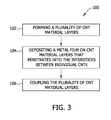
- FIG. 3 is a block diagram of an exemplary method of fabricating a bulk CNT and metallic composite strip.
- FIG. 1 illustrates an exemplary bulk carbon nanotube (CNT) and metallic composite 10 that includes a bulk CNT material layer 12 and one or more thin metal films or layers 14 .
- bulk CNT layer 12 includes opposed first and second sides 16 and 18 , respectively, and a layer of metal film 14 is deposited across each side 16 and 18 .
- FIG. 2 illustrates an exemplary bulk CNT and metallic composite strip 20 that is fabricated by welding bulk CNT layers 12 together, as will be described in more detail. The methods described herein produce a bulk CNT and metallic composite strip 20 that has a high weight-normalized electrical conductivity, a high thermal conductivity, and a high mechanical strength.
- bulk CNT layer 12 is fabricated from a plurality of metallic CNTs (not shown), such as “armchair” CNTs, that are each oriented with a chiral angle that is substantially parallel to the tube axis of each CNT.
- metallic CNTs such as “armchair” CNTs
- each formed CNT has an increased metallic character and has an increased capability for tremendously high current density.
- bulk CNT layer 12 may include a number of semi-conductor CNTs (not shown) in addition to the metallic CNTs.
- bulk CNT layer 12 is a non-woven sheet or a yarn.
- any other form of bulk CNT layer 12 may be used that enables composite 10 to function as described herein.
- metal film 14 is applied across CNT layer sides 16 and 18 and penetrates into the interstices between individual CNTs.
- the amount of metal used to form metal film 14 is enough to facilitate low electrical resistance interconnects between a substantial number of the CNTs.
- metal film 14 is a thin-film of aluminum that penetrates the bulk CNT layer 12 and coats a large fraction of the CNTs.
- metal film 14 may be any electrically conductive metal or combination of metals that enables bulk CNT and metallic composite 10 to function as described herein.
- metal film 14 is applied directly across CNT layer 12 via chemical vapor deposition and/or electroless plating.
- the process facilitates depositing metal within the interstices of the bulk CNT layer.
- metal film 14 may be applied via a sputtering and/or a physical vapor deposition process.
- any other metal deposition process may be used that enables bulk CNT and metallic composite 10 to function as described herein.
- multiple bulk CNT and metallic composites 10 are coupled together via a welding process that forms a bulk CNT and metallic composite strip 20 .
- a welding process that forms a bulk CNT and metallic composite strip 20 .
- three CNT and metallic composites 10 are coupled together along their sides 16 and/or 18 .
- CNT and metallic composites 10 may be joined in an end-to-end orientation (not shown).
- any number of CNT and metallic composites 10 may be coupled together to form a bulk CNT and metallic composite strip 20 with any desired length, width and/or thickness.
- CNT and metallic composites 10 are joined together via an ultrasonic welding process.
- CNT and metallic composites 10 are joined together via an ultrasonic additive manufacturing (UAM) process that sequentially couples layers of patterned metal together to produce net shape products having complex interior cavities.
- UAM ultrasonic additive manufacturing
- FIG. 3 illustrates an exemplary method 100 of fabricating a bulk CNT and metallic composite strip 20 .
- Method 100 includes forming 102 a plurality of CNT material layers 12 from a plurality of single-walled carbon nanotubes (SWCNTs) and/or multi-walled carbon nanotubes (MWCNTs).
- CNT material layers 12 are a non-woven sheet or a yarn.
- the method further includes depositing 104 a metal film 14 across one or more sides 16 and 18 of CNT material layer 12 to form a bulk CNT and metallic composite 10 .
- metal film 14 is deposited by at least one of a chemical vapor deposition, an electroless plating, a sputtering, and a physical vapor deposition process.
- the method also includes coupling 106 multiple bulk CNT and metallic composites 10 together to form a bulk CNT and metallic composite strip 20 .
- bulk CNT and metallic composites 10 are coupled together via at least one of an ultrasonic welding and an ultrasonic additive manufacturing process.
- non-woven sheets of bulk CNT material layers 12 are fabricated from individual SWCNTs having a diameter between about 2 nm and about 5 nm, individual MWCNTs having a diameter between about 20 nm and about 50 nm, or a combination of both.
- Each bulk CNT layer 12 is formed with a cross-sectional thickness of between about 20 ⁇ m and about 100 ⁇ m.
- a bulk CNT and metallic composite 10 is formed by coating each side 16 and 18 of bulk CNT layer 12 with approximately 3,000 ⁇ (0.3 ⁇ m) of metallic material.
- a metallic material such as aluminum, copper, nickel, titanium, silver, gold or chromium, or any combination thereof, may be used to form metallic composite 10 .
- any metallic material may be used that enables metallic composite 10 to function as described herein.
- the resulting bulk CNT and metallic composites 10 are coupled together via an ultrasonic welding process to form a bulk CNT and metallic composite strip 20 .
- the ultrasonic welding process facilitates reducing open space within composites 10 and reducing a thickness of each bulk CNT and metallic composite 10 by approximately 20%.
- bulk CNT and metallic composite 10 has a decreased electrical resistance between individual CNTs and a decreased electrical resistance.
- bulk CNT and metallic composite strip 20 is fabricated with dimensions measuring roughly one cm wide, 10 cm long, and is one to several composites 10 thick.
- a bulk CNT and metallic composite is fabricated with an increased specific electrical conductivity that is superior to other materials such as copper and aluminum.
- the composite exhibits a high electrical conductivity, a high thermal conductivity, and a high mechanical strength.
- the bulk CNT composite formed with the above techniques reduces contact resistance between individual CNTs and reduced open space within each bulk CNT and metallic composite.
- a plurality of bulk CNT and metallic composites are coupled to form a high strength, highly electrically conductive bulk CNT and metallic composite strip.
- the bulk CNT composite material having superior qualities makes it ideal for applications such as EMI shielding, wire conductors for power transmission line, spacecraft harness, and electric motors.
Abstract
Description
Claims (12)
Priority Applications (1)
| Application Number | Priority Date | Filing Date | Title |
|---|---|---|---|
| US14/461,760 US9129723B2 (en) | 2012-09-17 | 2014-08-18 | Method of fabricating bulk carbon nanotube and metallic composites |
Applications Claiming Priority (2)
| Application Number | Priority Date | Filing Date | Title |
|---|---|---|---|
| US13/621,585 US8865604B2 (en) | 2012-09-17 | 2012-09-17 | Bulk carbon nanotube and metallic composites and method of fabricating |
| US14/461,760 US9129723B2 (en) | 2012-09-17 | 2014-08-18 | Method of fabricating bulk carbon nanotube and metallic composites |
Related Parent Applications (1)
| Application Number | Title | Priority Date | Filing Date |
|---|---|---|---|
| US13/621,585 Division US8865604B2 (en) | 2012-09-17 | 2012-09-17 | Bulk carbon nanotube and metallic composites and method of fabricating |
Publications (2)
| Publication Number | Publication Date |
|---|---|
| US20140352869A1 US20140352869A1 (en) | 2014-12-04 |
| US9129723B2 true US9129723B2 (en) | 2015-09-08 |
Family
ID=48914413
Family Applications (2)
| Application Number | Title | Priority Date | Filing Date |
|---|---|---|---|
| US13/621,585 Active US8865604B2 (en) | 2012-09-17 | 2012-09-17 | Bulk carbon nanotube and metallic composites and method of fabricating |
| US14/461,760 Active US9129723B2 (en) | 2012-09-17 | 2014-08-18 | Method of fabricating bulk carbon nanotube and metallic composites |
Family Applications Before (1)
| Application Number | Title | Priority Date | Filing Date |
|---|---|---|---|
| US13/621,585 Active US8865604B2 (en) | 2012-09-17 | 2012-09-17 | Bulk carbon nanotube and metallic composites and method of fabricating |
Country Status (7)
| Country | Link |
|---|---|
| US (2) | US8865604B2 (en) |
| EP (1) | EP2896051B1 (en) |
| JP (1) | JP6346611B2 (en) |
| CN (1) | CN104603885B (en) |
| ES (1) | ES2650953T3 (en) |
| RU (1) | RU2639181C2 (en) |
| WO (1) | WO2014042755A1 (en) |
Cited By (1)
| Publication number | Priority date | Publication date | Assignee | Title |
|---|---|---|---|---|
| US20180189470A1 (en) * | 2015-07-01 | 2018-07-05 | Samsung Electronics Co., Ltd. | User authenticating method and device |
Families Citing this family (24)
| Publication number | Priority date | Publication date | Assignee | Title |
|---|---|---|---|---|
| US8853540B2 (en) * | 2011-04-19 | 2014-10-07 | Commscope, Inc. Of North Carolina | Carbon nanotube enhanced conductors for communications cables and related communications cables and methods |
| WO2017136806A1 (en) | 2016-02-04 | 2017-08-10 | General Nano Llc | Carbon nanotube sheet structure and method for its making |
| CN107000366B (en) | 2014-07-30 | 2019-04-23 | 一般纳米有限责任公司 | Carbon nanotube chip architecture and its manufacturing method |
| CN104942543B (en) * | 2015-06-15 | 2017-03-29 | 中国石油大学(华东) | The nanometer increasing material manufacturing method of upstream pumping mechanical seal |
| CN105150624B (en) * | 2015-08-12 | 2017-07-07 | 湖南深泰虹科技有限公司 | A kind of CNT, copper composite electromagnetic screen film and preparation method thereof |
| US10758936B2 (en) * | 2015-12-08 | 2020-09-01 | The Boeing Company | Carbon nanomaterial composite sheet and method for making the same |
| US9972420B2 (en) | 2015-12-08 | 2018-05-15 | The Boeing Company | Carbon nanotube shielding for transmission cables |
| US10685763B2 (en) | 2016-01-19 | 2020-06-16 | Xerox Corporation | Conductive polymer composite |
| US10418146B2 (en) | 2016-01-19 | 2019-09-17 | Xerox Corporation | Conductive polymer composite |
| US10186344B2 (en) | 2016-01-19 | 2019-01-22 | Xerox Corporation | Conductive polymer composite |
| US10796813B2 (en) | 2016-02-16 | 2020-10-06 | Xerox Corporation | Conductive polymer composite |
| US10234342B2 (en) * | 2016-04-04 | 2019-03-19 | Xerox Corporation | 3D printed conductive compositions anticipating or indicating structural compromise |
| JP7328703B2 (en) | 2017-07-21 | 2023-08-17 | ジェネラル ナノ エルエルシー | Conductive broads that provide lightning protection |
| US11820663B2 (en) | 2018-02-14 | 2023-11-21 | International Business Machines Corporation | Crystalline film of carbon nanotubes |
| US11424048B2 (en) * | 2018-06-28 | 2022-08-23 | Carlisle Interconnect Technologies, Inc. | Coaxial cable utilizing plated carbon nanotube elements and method of manufacturing same |
| JP7304366B2 (en) * | 2018-11-28 | 2023-07-06 | ホシデン株式会社 | High-frequency transmission device and high-frequency signal transmission method |
| CN111696700A (en) * | 2019-03-12 | 2020-09-22 | 泰连服务有限公司 | Metal structure having a desired combination of mechanical and electrical properties |
| US11843153B2 (en) | 2019-03-12 | 2023-12-12 | Te Connectivity Solutions Gmbh | Use of enhanced performance ultraconductive copper materials in cylindrical configurations and methods of forming ultraconductive copper materials |
| CN110283347B (en) * | 2019-05-08 | 2022-02-01 | 广东石油化工学院 | Elastic electromagnetic shielding film and preparation method thereof |
| CN110337234B (en) * | 2019-07-09 | 2020-11-06 | 中国科学院苏州纳米技术与纳米仿生研究所 | Damp-heat-resistant electromagnetic shielding film, composite material, preparation method and application thereof |
| EP3839649A1 (en) * | 2019-12-20 | 2021-06-23 | Nivarox-FAR S.A. | Rigid timepiece component for oscillator mechanism or for escapement mechanism and clockwork comprising such a component |
| EP3839643B1 (en) * | 2019-12-20 | 2024-02-21 | The Swatch Group Research and Development Ltd | Flexible timepiece component and clockwork comprising such a component |
| CN111462938B (en) * | 2020-04-17 | 2021-09-14 | 珠海蓉胜超微线材有限公司 | Copper-coated carbon nano composite flat wire and preparation method thereof |
| CN111599531A (en) * | 2020-05-29 | 2020-08-28 | 珠海蓉胜超微线材有限公司 | Copper-coated carbon nano composite wire and preparation method thereof |
Citations (6)
| Publication number | Priority date | Publication date | Assignee | Title |
|---|---|---|---|---|
| US20060172179A1 (en) | 2003-09-08 | 2006-08-03 | Intematix Corporation | Low platinum fuel cells, catalysts, and method for preparing the same |
| US20090008712A1 (en) | 2007-06-22 | 2009-01-08 | Samusung Electronics, Co., Ltd. | Carbon nano-tube (cnt) thin film comprising metallic nano-particles, and a manufacturing method thereof |
| US20090035555A1 (en) | 2007-08-03 | 2009-02-05 | Sean Imtiaz Brahim | Electrically conductive transparent coatings comprising organized assemblies of carbon and non-carbon compounds |
| US20090196985A1 (en) | 2008-02-01 | 2009-08-06 | Tsinghua University | Method for making individually coated and twisted carbon nanotube wire-like structure |
| WO2010101418A2 (en) | 2009-03-04 | 2010-09-10 | Ls Cable Ltd. | Composition for conductive paste containing nanometer-thick metal microplates |
| US20110198542A1 (en) | 2010-02-18 | 2011-08-18 | Samsung Electronics Co., Ltd. | Conductive carbon nanotube-metal composite ink |
Family Cites Families (18)
| Publication number | Priority date | Publication date | Assignee | Title |
|---|---|---|---|---|
| US7518247B2 (en) * | 2002-11-29 | 2009-04-14 | Nec Corporation | Semiconductor device and its manufacturing method |
| US20050112450A1 (en) * | 2003-09-08 | 2005-05-26 | Intematix Corporation | Low platinum fuel cell catalysts and method for preparing the same |
| JP4412052B2 (en) * | 2003-10-28 | 2010-02-10 | 富士ゼロックス株式会社 | Composite material and method for producing the same |
| JP2005277096A (en) * | 2004-03-24 | 2005-10-06 | Japan Science & Technology Agency | Semiconductor interconnection constituted by use of metal film containing carbon nanotube and its manufacturing method, and method of manufacturing metal film containing carbon nanotube |
| JP4711165B2 (en) * | 2004-06-21 | 2011-06-29 | 日立金属株式会社 | High thermal conductivity / low thermal expansion composite and method for producing the same |
| CN100503872C (en) * | 2004-11-09 | 2009-06-24 | 岛根县 | Metal-based carbon fiber composite material production method |
| JP2007049084A (en) * | 2005-08-12 | 2007-02-22 | Toshiba Corp | Switch element, memory device, and magnetoresistance effect element |
| JP5289678B2 (en) * | 2006-01-12 | 2013-09-11 | 富士通株式会社 | Field effect transistor |
| JP5157074B2 (en) * | 2006-03-16 | 2013-03-06 | 富士通株式会社 | Field effect transistor and manufacturing method thereof |
| JP2008303081A (en) * | 2007-06-05 | 2008-12-18 | Sonac Kk | Carbon nanotube assembly |
| JP4589439B2 (en) * | 2008-02-01 | 2010-12-01 | ツィンファ ユニバーシティ | Method for producing carbon nanotube composite |
| CN101712468B (en) * | 2008-09-30 | 2014-08-20 | 清华大学 | Carbon nanotube composite material and preparation method thereof |
| JP2010114316A (en) * | 2008-11-07 | 2010-05-20 | Toyota Motor Corp | Photovoltaic device and method of manufacturinig the same |
| WO2010136899A1 (en) * | 2009-05-29 | 2010-12-02 | The Governors Of The University Of Alberta | Reinforced composites and methods of making and using thereof |
| CN102040212B (en) * | 2009-10-23 | 2013-01-09 | 清华大学 | Carbon nano tube composite structure |
| JP2011243689A (en) * | 2010-05-17 | 2011-12-01 | Panasonic Corp | Semiconductor device and method of manufacturing the same |
| RU2475445C2 (en) * | 2010-12-20 | 2013-02-20 | Государственное образовательное учреждение высшего профессионального образования "Тамбовский государственный университет имени Г.Р. Державина" | Method for obtaining volume nanostructured material |
| EP2660361A1 (en) * | 2010-12-28 | 2013-11-06 | National Institute of Advanced Industrial Science And Technology | Carbon nanotube metal composite material and production method for same |
-
2012
- 2012-09-17 US US13/621,585 patent/US8865604B2/en active Active
-
2013
- 2013-07-08 RU RU2014147110A patent/RU2639181C2/en active
- 2013-07-08 WO PCT/US2013/049551 patent/WO2014042755A1/en active Application Filing
- 2013-07-08 JP JP2015531920A patent/JP6346611B2/en active Active
- 2013-07-08 EP EP13744866.8A patent/EP2896051B1/en active Active
- 2013-07-08 ES ES13744866.8T patent/ES2650953T3/en active Active
- 2013-07-08 CN CN201380038990.1A patent/CN104603885B/en active Active
-
2014
- 2014-08-18 US US14/461,760 patent/US9129723B2/en active Active
Patent Citations (6)
| Publication number | Priority date | Publication date | Assignee | Title |
|---|---|---|---|---|
| US20060172179A1 (en) | 2003-09-08 | 2006-08-03 | Intematix Corporation | Low platinum fuel cells, catalysts, and method for preparing the same |
| US20090008712A1 (en) | 2007-06-22 | 2009-01-08 | Samusung Electronics, Co., Ltd. | Carbon nano-tube (cnt) thin film comprising metallic nano-particles, and a manufacturing method thereof |
| US20090035555A1 (en) | 2007-08-03 | 2009-02-05 | Sean Imtiaz Brahim | Electrically conductive transparent coatings comprising organized assemblies of carbon and non-carbon compounds |
| US20090196985A1 (en) | 2008-02-01 | 2009-08-06 | Tsinghua University | Method for making individually coated and twisted carbon nanotube wire-like structure |
| WO2010101418A2 (en) | 2009-03-04 | 2010-09-10 | Ls Cable Ltd. | Composition for conductive paste containing nanometer-thick metal microplates |
| US20110198542A1 (en) | 2010-02-18 | 2011-08-18 | Samsung Electronics Co., Ltd. | Conductive carbon nanotube-metal composite ink |
Non-Patent Citations (2)
| Title |
|---|
| International Search Report and Written Opinion of International Application No. PCT/US2013/049551; Sep. 4, 2013; 9 pages. |
| PCT International Preliminary Report on Patentability for related application PCT/US2013/049551 dated Mar. 17, 2015; 5 p. |
Cited By (2)
| Publication number | Priority date | Publication date | Assignee | Title |
|---|---|---|---|---|
| US20180189470A1 (en) * | 2015-07-01 | 2018-07-05 | Samsung Electronics Co., Ltd. | User authenticating method and device |
| US10891363B2 (en) * | 2015-07-01 | 2021-01-12 | Samsung Electronics Co.. Ltd. | User authenticating method and device |
Also Published As
| Publication number | Publication date |
|---|---|
| JP2016500582A (en) | 2016-01-14 |
| ES2650953T3 (en) | 2018-01-23 |
| WO2014042755A1 (en) | 2014-03-20 |
| RU2639181C2 (en) | 2017-12-20 |
| JP6346611B2 (en) | 2018-06-20 |
| EP2896051A1 (en) | 2015-07-22 |
| RU2014147110A (en) | 2016-11-10 |
| US8865604B2 (en) | 2014-10-21 |
| CN104603885A (en) | 2015-05-06 |
| EP2896051B1 (en) | 2017-09-06 |
| US20140352869A1 (en) | 2014-12-04 |
| US20140080378A1 (en) | 2014-03-20 |
| CN104603885B (en) | 2017-08-08 |
Similar Documents
| Publication | Publication Date | Title |
|---|---|---|
| US9129723B2 (en) | Method of fabricating bulk carbon nanotube and metallic composites | |
| US7750240B2 (en) | Coaxial cable | |
| US9193586B2 (en) | Cable | |
| TWI345792B (en) | Cable | |
| US20160086695A1 (en) | Electrically and Thermally Non-Metallic Conductive Nanostructure-Based Adapters | |
| US9299473B2 (en) | Composite electrically conductive structures | |
| TWI345793B (en) | Cable | |
| JP2016500582A5 (en) | ||
| US20140314949A1 (en) | Carbon nanotube conductor with enhanced electrical conductivity | |
| EP2085979B1 (en) | Coaxial cable and method for making the same | |
| WO2019083038A1 (en) | Carbon nanotube composite wire, carbon nanotube-coated electric wire, and wire harness | |
| TW201900544A (en) | Semiconductor device | |
| JP2017171546A (en) | Carbon nanotube wire and carbon nanotube wire-connected structure | |
| TWI424954B (en) | Carbon nanotube composite structure | |
| US20200251248A1 (en) | Coated carbon nanotube electric wire | |
| JP7203748B2 (en) | Carbon nanotube coated wire | |
| JP7254708B2 (en) | Carbon nanotube composite wire, carbon nanotube coated wire and wire harness | |
| JP7214644B2 (en) | Carbon nanotube composite wires, carbon nanotube coated wires, wire harnesses, wiring for robots and overhead wires for trains | |
| JP2017183281A (en) | Carbon nanotube wire rod and carbon nanotube wire rod connection structure | |
| JP6719244B2 (en) | Carbon nanotube wire connecting method and carbon nanotube wire connecting structure | |
| WO2019083029A1 (en) | Carbon nanotube coated electric wire | |
| US20200258656A1 (en) | Coated carbon nanotube electric wire | |
| JP2020181687A (en) | Carbon nanotube wire material, carbon nanotube wire material connecting structure, and manufacturing method of carbon nanotube wire material | |
| WO2019083034A1 (en) | Carbon-nanotube covered electric wire | |
| JP2020167160A (en) | Connection structure |
Legal Events
| Date | Code | Title | Description |
|---|---|---|---|
| AS | Assignment |
Owner name: THE BOEING COMPANY, ILLINOIS Free format text: ASSIGNMENT OF ASSIGNORS INTEREST;ASSIGNOR:WASYNCZUK, JAMES ANTONI;REEL/FRAME:033554/0001 Effective date: 20140815 |
|
| FEPP | Fee payment procedure |
Free format text: PAYOR NUMBER ASSIGNED (ORIGINAL EVENT CODE: ASPN); ENTITY STATUS OF PATENT OWNER: LARGE ENTITY |
|
| STCF | Information on status: patent grant |
Free format text: PATENTED CASE |
|
| MAFP | Maintenance fee payment |
Free format text: PAYMENT OF MAINTENANCE FEE, 4TH YEAR, LARGE ENTITY (ORIGINAL EVENT CODE: M1551); ENTITY STATUS OF PATENT OWNER: LARGE ENTITY Year of fee payment: 4 |
|
| MAFP | Maintenance fee payment |
Free format text: PAYMENT OF MAINTENANCE FEE, 8TH YEAR, LARGE ENTITY (ORIGINAL EVENT CODE: M1552); ENTITY STATUS OF PATENT OWNER: LARGE ENTITY Year of fee payment: 8 |