US9059799B2 - Apparatus and method to calculate a noise figure of an optical amplifier for wavelength channels in a partial-fill scenario to account for channel loading - Google Patents
Apparatus and method to calculate a noise figure of an optical amplifier for wavelength channels in a partial-fill scenario to account for channel loading Download PDFInfo
- Publication number
- US9059799B2 US9059799B2 US13/091,690 US201113091690A US9059799B2 US 9059799 B2 US9059799 B2 US 9059799B2 US 201113091690 A US201113091690 A US 201113091690A US 9059799 B2 US9059799 B2 US 9059799B2
- Authority
- US
- United States
- Prior art keywords
- noise
- channels
- fill
- gain
- wavelengths
- Prior art date
- Legal status (The legal status is an assumption and is not a legal conclusion. Google has not performed a legal analysis and makes no representation as to the accuracy of the status listed.)
- Active, expires
Links
Images


Classifications
-
- H—ELECTRICITY
- H04—ELECTRIC COMMUNICATION TECHNIQUE
- H04B—TRANSMISSION
- H04B10/00—Transmission systems employing electromagnetic waves other than radio-waves, e.g. infrared, visible or ultraviolet light, or employing corpuscular radiation, e.g. quantum communication
- H04B10/25—Arrangements specific to fibre transmission
- H04B10/2507—Arrangements specific to fibre transmission for the reduction or elimination of distortion or dispersion
-
- H—ELECTRICITY
- H04—ELECTRIC COMMUNICATION TECHNIQUE
- H04B—TRANSMISSION
- H04B10/00—Transmission systems employing electromagnetic waves other than radio-waves, e.g. infrared, visible or ultraviolet light, or employing corpuscular radiation, e.g. quantum communication
- H04B10/07—Arrangements for monitoring or testing transmission systems; Arrangements for fault measurement of transmission systems
- H04B10/075—Arrangements for monitoring or testing transmission systems; Arrangements for fault measurement of transmission systems using an in-service signal
- H04B10/079—Arrangements for monitoring or testing transmission systems; Arrangements for fault measurement of transmission systems using an in-service signal using measurements of the data signal
- H04B10/0797—Monitoring line amplifier or line repeater equipment
-
- H—ELECTRICITY
- H04—ELECTRIC COMMUNICATION TECHNIQUE
- H04J—MULTIPLEX COMMUNICATION
- H04J14/00—Optical multiplex systems
- H04J14/02—Wavelength-division multiplex systems
-
- H—ELECTRICITY
- H01—ELECTRIC ELEMENTS
- H01S—DEVICES USING THE PROCESS OF LIGHT AMPLIFICATION BY STIMULATED EMISSION OF RADIATION [LASER] TO AMPLIFY OR GENERATE LIGHT; DEVICES USING STIMULATED EMISSION OF ELECTROMAGNETIC RADIATION IN WAVE RANGES OTHER THAN OPTICAL
- H01S3/00—Lasers, i.e. devices using stimulated emission of electromagnetic radiation in the infrared, visible or ultraviolet wave range
-
- H—ELECTRICITY
- H04—ELECTRIC COMMUNICATION TECHNIQUE
- H04B—TRANSMISSION
- H04B10/00—Transmission systems employing electromagnetic waves other than radio-waves, e.g. infrared, visible or ultraviolet light, or employing corpuscular radiation, e.g. quantum communication
- H04B10/29—Repeaters
- H04B10/291—Repeaters in which processing or amplification is carried out without conversion of the main signal from optical form
- H04B10/293—Signal power control
- H04B10/294—Signal power control in a multiwavelength system, e.g. gain equalisation
- H04B10/296—Transient power control, e.g. due to channel add/drop or rapid fluctuations in the input power
Definitions
- Optical transmission systems constitute the basic carrier for most telecommunication systems.
- Many optical transmission technologies are based on the principle of wavelength division multiplexing (WDM) or Dense WDM (DWDM), where the transmission channels are carried by optical signals over different wavelengths or different bands of wavelengths.
- the optical signals are initially modulated at the transmitter end of the optical network, propagated through the network via an optical link or fiber, and then detected at the receiver end.
- the optical signal may also be amplified before or after transmission to enhance performance, for example to compensate for attenuation or noise during transport.
- Erbium Doped Fiber Amplifiers are one type of optical amplifiers that are commonly used in optical systems. However, EDFAs may also contribute noise in the optical signals, which needs to be accounted for.
- the disclosure includes an apparatus.
- the apparatus includes a processor configured to calculate a noise figure of an optical amplifier for a plurality of selected wavelength channels in a partial-fill scenario that accounts for channel loading.
- the noise figure is calculated using a plurality of corresponding noise figure correction values at a plurality of wavelengths based on an effective number of channels.
- the disclosure includes a network component.
- the network component includes a processor configured to calculate a gain correction for a gain caused by an optical amplifier for a plurality of selected wavelength channels in a partial-fill scenario that accounts for channel loading.
- the gain correction is based on a spectral hole burning effect model that is calculated for a range of wavelengths based on a number of the selected wavelength channels.
- the disclosure includes a method.
- the method includes calculating an effective number of channels for a plurality of wavelengths.
- the method also includes calculating a noise figure correction for the wavelengths based on the effective number of channels.
- the method further includes adjusting a noise figure that corresponds to an optical amplifier using the noise figure correction.
- FIG. 1 is a schematic diagram of an embodiment of an optical communications system.
- FIG. 2 is a chart of an embodiment of a full-fill noise figure.
- FIG. 3 is a chart of an embodiment of a full-fill gain ripple.
- FIG. 4 is a schematic diagram of an embodiment of a measurement apparatus.
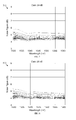
- FIG. 5 is a chart of an embodiment of a partial-fill noise figure.
- FIG. 6 is a chart of another embodiment of a partial-fill noise figure.
- FIG. 7 is a chart of another embodiment of a partial-fill noise figure.
- FIG. 8 is a chart of another embodiment of a partial-fill noise figure.
- FIG. 9 is a chart of another embodiment of a partial-fill noise figure.
- FIG. 10 is a chart of another embodiment of a partial-fill noise figure.
- FIG. 11 is a chart of an embodiment of a partial-fill gain ripple.
- FIG. 12 is a chart of another embodiment of full-fill gain error.
- FIG. 13 is a chart of an embodiment of a noise figure difference.
- FIG. 14 is a chart of another embodiment of a noise figure difference.
- FIG. 15 is a chart of another embodiment of a partial-fill noise figure.
- FIG. 16 is a chart of another embodiment of a partial-fill noise figure.
- FIG. 17 is a chart of an embodiment of a noise figure difference.
- FIG. 18 is a chart of another embodiment of a noise figure difference.
- FIG. 19 is a chart of another embodiment of a noise figure difference.
- FIG. 20 is a chart of another embodiment of a noise figure difference.
- FIG. 21 is a chart of an embodiment of a gain correction.
- FIG. 22 is a flowchart of an embodiment of a partial filled noise figure and gain modeling method.
- FIG. 23 is a schematic diagram of an embodiment of a general-purpose computer system.
- EDFAs may be deployed in optical communications systems, such as in various locations on the optical links. Understanding and modeling of EDFAs' performance and characteristics, such as noise and gain characteristics, may be critical to improve the optical communications systems' network design and control.
- the EDFA's characteristics may comprise the EDFA's noise figure, which may be used to calculate the optical links or the system's optical signal to noise ratio (OSNR).
- the EDFA's characteristics may also comprise the EDFA's gain, which may be used to calculate the OSNR, the power ripple, and/or dynamic range requirement of a channel actuator for OSNR equalization.
- the noise figure may be a function of the EDFA's operating conditions, which may be based on wavelength, gain, input power, gain tilt, and/or channel loading.
- the noise figure's dependence on wavelength, gain, input power, and/or gain tilt may be modeled under a full-fill condition, which may not include the noise figure's dependence on channel loading.
- Channel loading may correspond to the specific set of wavelength channels used or selected to transmit signals.
- a typically derived and used multi-dimensional noise figure model may be valid for the full-fill condition but ignore channel loading, and thus may not be sufficiently accurate to reflect the actual noise in the system.
- the gain may also be modeled under the full-fill condition. However, due to spectral hole burning (SHB) effects, the gain may also substantially depend on channel loading. For instance, the gain change caused by SHB may exceed the full-fill peak-to-peak gain ripple specification. Thus, the full-fill gain model may also include errors with respect to the actual gain in the system.
- SHB spectral hole burning
- FIG. 1 illustrates an embodiment of an optical communications system 100 that may use EDFAs to boost optical signals on optical links.
- the optical communications system 100 may be a WDM or DWDM system and may be a part of a wavelength switched optical network (WSON) or a passive optical network (PON).
- the optical communications system 100 may comprise an express channel source/input 110 , a first multiplexer 112 , a first wavelength selective switch (WSS) 120 , one or more first EDFAs 130 , a splitter 140 , a demultiplexer 142 , a second multiplexer 144 , a second WSS 150 , and a second EDFA 160 .
- the components of the optical communications system 100 may be arranged as shown in FIG. 1 .
- the express channel source/input 110 , first multiplexer 112 , and first WSS 120 may be located at a first provider site, where the first multiplexer 112 may be coupled to one or more transmitters (TX) (not shown).
- the first EDFAs 130 may be coupled to an optical link that extends from the first WSS 120 to the splitter 140 .
- the splitter 140 , demultiplexer 142 , and second multiplexer 144 may be located at a customer or distribution site, where the demultiplexer 142 may be coupled to one or more receivers (RX) (not shown).
- the second WSS 150 and second multiplexer 144 may be coupled to one or more transmitters (TX), for instance at the same customer or distribution site or at a second provider site that is coupled to the customer or distribution site.
- the second EDFA 160 may be coupled to a second optical link that extends from the second WSS 150 , e.g., to a second customer or distribution site (not shown).
- the express channel source/input 110 may be a data channel and/or a carrier for data channels.
- the first multiplexer 112 may be any device or component configured to combine a plurality of different wavelength channels from one or more transmitters into a single combined channel and redirect the single combined channel to the first WSS 120 .
- the different wavelength channels may be data channels that may be transmitted from one or a plurality of transmitters coupled to the first multiplexer 112 .
- the first WSS 120 may be any device or component configured to combine the single combined channel from the first multiplexer 112 and the express channel 110 into a signal, and transmit the signal on the optical link that is coupled to the first WSS 120 .
- the first EDFAs 130 may be configured to boost or amplify the combined signal from the first WSS 120 that is transmitted on the optical link.
- the splitter 140 may be any device or component configured to split the received combined signal on the optical link into the single combined channel and the express channel 110 and redirect the single combined channel to the demultiplexer 142 and the express channel to the second WSS 150 .
- the demultiplexer 142 may be any device or component configured to split the single combined channel into the different wavelength channels and redirect the wavelength channels to one or more receivers.
- the second WSS 150 may be configured similar to the first WSS 120 .
- the second WSS 150 may combine the express channel 110 from the splitter 140 and a single combined channel from the second multiplexer 144 into a combined signal, and transmit the combined signal on the second optical link that is coupled to the second WSS 150 .
- the second multiplexer 144 may be configured similar to the first multiplexer 112 .
- the second multiplexer 144 may combine a plurality of different wavelength channels from one or more transmitters into the single combined channel and redirect the single combined channel to the second WSS 150 .
- the second EDFAs 160 may be configured similar to the first EDFAs 130 .
- the second EDFAs 160 may boost or amplify the combined signal from the second WSS 150 that is transmitted on the second optical link.
- the optical communications system 100 or at least some of its components may be designed and/or controlled based on the noise and gain characteristics of the first EDFAs 130 and the second EDFA 160 based on full-fill conditions models, e.g., without accounting to channel loading and/or SHB effects.
- the component of the optical communications system 100 may be designed and/or controlled according to a full-fill noise figure model, a full-fill gain ripple model, or both.
- FIG. 2 illustrates one embodiment of a full-fill noise figure 200 for an EDFA, such as the first EDFAs 130 and/or the second EDFA 160 .
- FIG. 2 shows a plurality of curves for a plurality of different EDFA gains that range from about 20 decibel (dB) to about 32 dB (as indicated in the legend).
- Each curve represents a full-fill noise figure (in dB) as a function of wavelengths that extend from about 1,530 nanometers (nm) to about 1560 nm.
- the gain tilt and per channel output power for all curves is about the same.
- the curves indicate that the noise figure may be sensitive to wavelength and gain at the lower gain values (e.g., closer to about 20 dB). At the higher gain values (e.g., closer to about 32 dB), the noise figure is relatively constant and may not be sensitive to wavelength and/or gain.
- FIG. 3 illustrates one embodiment of a full-fill gain ripple 300 for an EDFA, such as the first EDFAs 130 and/or the second EDFA 160 .
- FIG. 3 shows a plurality of curves for the same gains in FIG. 2 (e.g., ranging from about 20 dB to about 30 dB). Each curve represents a signal gain ripple or variation (in dB) in the full-fill condition as a function of wavelength, which extends from about 1,525 nm to about 1565 nm.
- the gain ripple curves correspond to the first six noise figure curves in FIG. 2 and are obtained under similar conditions.
- the gain ripple curves indicate that the gain is relatively constant and may not be sensitive to wavelength and/or gain over substantially the entire gain range from about 20 dB to about 30 dB. Specifically, in some embodiment, the variations in the gain values for the different gains range from about ⁇ 0.1 dB to about 0.2 dB, which may be substantially small. In other embodiments, the variations in the gain values for the different gains may be larger.
- FIG. 4 illustrates an embodiment of a measurement apparatus 400 .
- the measurement apparatus 400 may be used to measure the noise figure and gain ripple of an EDFA in the partial-fill condition, which may include channel loading effects.
- the measurement apparatus 400 may comprise a multichannel source 410 , a splitter 420 , a WSS 430 , an EDFA 440 , and an optical spectrum analyzer (OSA) 450 , which may be arranged as shown in FIG. 4 .
- OSA optical spectrum analyzer
- the multichannel source 410 may be configured to transmit a plurality of wavelength channels, e.g., optical signals, that extend a range of wavelengths, e.g., from about 1,530 nm to about 1,560 nm.
- the splitter 420 may be configured to split the power of the wavelength channels from the multichannel source 410 into two portions. A first portion may be forwarded directly to the WSS 430 and a second portion may be forwarded via a variable optical amplifier (VOA) to the WSS 430 .
- VOA variable optical amplifier
- the VOA may attenuate the wavelength channels differently, e.g., introduce different losses to the wavelength channels, according to a determined spectrum profile.
- the two portions may then be combined at the WSS 430 to extend or increase the attenuation dynamic range of the WSS 430 .
- the multichannel source 410 may be coupled directly to the WSS 430 , without using the splitter 420 , if the WSS 430 has sufficient dynamic attenuation range.
- the WSS 430 may be configured to select some of the wavelength channels, e.g., a subset of channels from the range of wavelengths, that may determine the channel loading. Specifically, the WSS 430 may transmit the selected wavelength channels at substantially higher power than the remaining non-selected wavelength channels.
- the selected wavelength channels are designated in FIG. 4 as signal channels.
- the remaining non-selected wavelength channels may be used as probe channels and may have larger than zero power.
- the wavelength channels may be transmitted to the EDFA 440 , which may amplify the wavelength channels and forward the wavelength channels to the OSA 450 .
- the OSA 450 may be used to measure the partial-fill noise figure and gain of the wavelength channels that correspond to the selected channel loading of the wavelength channels.
- the total power of the probe channels transmitted from the WSS 430 may be negligible compared to the power of the transmitted signal channels to ensure that the probe channels do not affect the EDFA 440 operating conditions. However, the total power of the probe channels may be high enough at the output of the EDFA 440 to ensure that the noise figure and gain measurements at the OSA 450 are sufficiently accurate.
- the measurement apparatus 400 may be used to obtain the noise figure and/or gain measurements (as a function of wavelength) for a plurality of different channel loading conditions, e.g., for different sets of selected wavelength or signal channels.
- FIG. 5 illustrates an example of a partial-fill noise figure 500 that may be measured for the EDFA 440 using the measurement apparatus 400 .
- FIG. 5 shows a plurality of curves for a plurality of different channel loading conditions, e.g., different sets of selected wavelength or signal channels. Specifically, the curves are measured at a EDFA gain of about 20 dB. The circles on the curves indicate the selected signal channels and the remaining data on the curves may correspond to the probe channels.
- Each curve represents a partial-fill noise figure (in dB) as a function of wavelength that extends from about 1,530 nm to about 1,560 nm. The curves indicate that the noise figure may be more dependent on the channel loading at shorter wavelengths, where higher variations or fluctuations in the noise figure value occur. For example, the variations at shorter wavelengths may reach about two dB.
- FIG. 6 illustrates an example of another partial-fill noise FIG. 600 that may be measured for the EDFA 440 using the measurement apparatus 400 .
- FIG. 6 shows a plurality of curves for the same channel loading conditions in the partial-fill noise FIG. 500 and that correspond to an EDFA gain of about 22 dB. Similar to the partial-fill noise FIG. 500 , the curves of the partial-fill noise FIG. 600 extend from about 1,530 nm to about 1,560 nm. The curves also indicate that the noise figure may be more dependent on the channel loading at shorter wavelengths. However, the variations in the values of the partial-fill noise FIG. 600 at the lower wavelengths are less than the variations in the values of the partial-fill noise FIG. 500 .
- FIG. 7 illustrates an example of another partial-fill noise figure 700 that may be measured for the EDFA 440 using the noise figure and gain measurement apparatus 400 .
- FIG. 7 shows a plurality of curves for the same channel loading conditions in the partial-fill noise figure 500 and that correspond to an EDFA gain of about 24 dB. The curves also indicate that the noise figure may be more dependent on the channel loading at shorter wavelengths, but the variations in the values are less than the variations in the values of the partial-fill noise figure 500 and the partial-fill noise figure 600 .
- FIG. 8 illustrates an example of another partial-fill noise figure 800 that may be measured for the EDFA 440 .
- FIG. 8 shows a plurality of curves for the same channel loading conditions in the partial-fill noise figure 500 and that correspond to an EDFA gain of about 26 dB. The curves also indicate that the noise figure may be more dependent on the channel loading at shorter wavelengths, but the variations in the values are less than the variations in the values of the partial-fill noise figure 700 .
- FIGS. 9 and 10 also illustrate examples of a partial-fill noise FIG. 900 and a partial-fill noise FIG. 1000 , respectively, that may be measured for the EDFA 440 .
- FIGS. 9 and 10 show a plurality of curves for the same channel loading conditions in the partial-fill noise FIG. 500 and that correspond to a gain of about 28 dB and about 30 dB, respectively. The curves indicate less dependency of the noise figure on the channel loading at shorter wavelengths in comparison to the partial-fill noise FIG. 700 .
- the partial-fill noise FIGS. 500 , 600 , 700 , 800 , 900 , and 1000 reveal a pattern of dependency of noise figure on channel loading at shorter wavelengths and a decrease in that dependency at higher gains.
- FIG. 11 illustrates an example of a partial-fill gain ripple 1100 that may be measured for the EDFA 440 using the measurement apparatus 400 .
- FIG. 11 shows a plurality of curves for similar channel loading conditions in the partial-fill noise figure 500 . Specifically, the curves are measured for an EDFA gain of about 30 dB and a gain tilt of about ⁇ 1 dB.
- FIG. 11 also shows a full-fill gain curve 1110 , for a similar gain tilt of about ⁇ 1 dB.
- the full-fill gain curve is measured based on a full-fill condition using the entire set of wavelength channels in the range from about 1,530 nm to about 1,560 nm.
- FIG. 11 reveals a substantial difference between the measured curves for the partial-fill case that accounts for selected channel loading and the full-fill gain curve 1110 that is based on all the available wavelength channels.
- FIG. 12 illustrates an example of partial-fill gain error 1200 with respect to the full-fill conditions.
- FIG. 11 shows a plurality of gain curves for the same channel loading conditions of the partial-fill gain ripple 1100 .
- the error curves represent the differences between the corresponding partial-fill gain curves and the full-fill gain curve 1110 .
- the error curves reveal substantial errors between the measured partial-fill gain values and the full-fill gain values.
- the gain error may be up to about 0.8 dB. Since, the gain error may be cumulative in a cascaded EDFA setup, such as the cascaded EDFAs 130 on the optical link, the total or cumulative gain error between the partial-fill and full-fill conditions may become substantially large.
- the relationship between the noise figure and the channel loading may be complicated, e.g., due to the relatively large number of different possible combinations of wavelength channels for channel loading. Thus, obtaining an accurate partial-fill model that considers the various possible channel loading conditions may be difficult. However, a relationship between the noise figure and the quantity of wavelength channels that are used for channel loading may be obtained. Specifically, a larger noise figure difference or error between the partial-fill case and the full-fill case may be observed as fewer wavelength channels are selected for channel loading, as described below.
- FIG. 13 illustrates an example of a noise figure difference 1300 that may be calculated for multiple channel loading conditions with different number of selected wavelength channels.
- FIG. 13 shows the difference in values between each of a plurality of partial-fill gain figure curves for different numbers of selected wavelength channels and a full-fill gain figure curve for all the available wavelength channels.
- the partial-fill gain figure curves correspond to a range of channel conditions from about one selected wavelength channel to about 40 selected wavelength channels.
- the full-fill noise figure curve corresponds to using all the about 40 wavelength channels.
- the difference values for each channel loading condition are calculated for the same wavelength signal about 1,529.55 nm, e.g., at the lower wavelength range. Accordingly, all the considered channel loading conditions comprise a selected wavelength channel at about 1,529.55 nm.
- the difference values vs. the number of wavelength channels are represented by circles.
- the circles that correspond to the same number of wavelength channels may not correspond to the same set of selected wavelength channels and may not have equal difference values (e.g., are not aligned on the y-axis).
- the values reveal an increase in the full-fill and partial-fill noise figure difference or error as the quantity of used wavelength channels decreases.
- the partial-fill noise figure may match the full-fill noise figure and thus the difference value may be equal to about zero.
- FIG. 14 illustrates an example of another full-fill and partial-fill noise figure difference 1400 that may be calculated for multiple channel loading conditions with different number of wavelength channels.
- FIG. 14 shows the difference in values between each of a plurality of partial-fill noise figure curves for different number of selected wavelength channels and a full-fill noise figure curve.
- the partial-fill noise figure curves and the full-fill noise figure curve correspond to the same sets of selected wavelength channels of the noise figure difference 1300 .
- the difference values for each channel loading condition are calculated for a wavelength signal at about 1,560.61 nm, e.g., at the higher wavelength range.
- the values of the noise figure difference 1400 reveal an increase in the full-fill and partial-fill noise figure difference or error as the quantity of used wavelength channels decreases. Since a similar pattern of increased noise figure difference with decreased number of wavelength channels was observed for the both the lower wavelength range and the higher wavelength range, this relationship between noise figure difference and quantity of selected wavelength channels may be independent of signal wavelength.
- FIG. 15 illustrates an example of another partial-fill noise figure 1500 .
- the partial-fill noise figure 1500 corresponds to using a single wavelength channel for channel loading. Two curves are shown for two cases of individually selected wavelength channels at about 1,530 nm and about 1,560 nm. The measured values of the partial-fill noise figure 1500 are shown for a plurality of wavelengths in the range from about 1,530 nm to about 1,560 nm. The circles on the curves indicate the selected signal channels and the remaining data on the curves may correspond to the probe channels.
- FIG. 15 shows that the curve that corresponds to the higher selected wavelength has higher noise values.
- FIG. 16 illustrates an example of another partial-fill noise figure 1600 .
- the two signal channels partial-fill noise figure 1600 corresponds to using two wavelength channels for channel loading. Three curves are shown for three cases of two selected wavelength channels.
- the measured values of the partial-fill noise figure 1600 are shown for a plurality of wavelengths in the range from about 1,530 nm to about 1,560 nm.
- the circles on the curves indicate the selected signal channels and the remaining data on the curves may correspond to the probe channels.
- FIG. 16 also shows that the curves that correspond to higher selected wavelengths have higher noise values.
- FIGS. 15 and 16 reveal that using a smaller wavelength for channel loading may further reduce the noise figure value in comparison to using a larger wavelength. For instance, selecting a set of smaller wavelength channels may result in a smaller noise figure than selecting a set of larger wavelength channels with the same number of wavelengths.
- ⁇ ref is a reference wavelength and c 0 and c 1 are constants that may be empirically determined.
- the effective number of channels may not correspond or match the actual number of channels used for channel loading.
- FIG. 17 illustrates an example of another noise figure difference 1700 .
- the noise figure difference 1700 is obtained by plotting the values of the noise figure difference 1300 vs. a sequence of calculated effective number of channels according to equation (1).
- the effective number of channels, or n eff is a function of the wavelength channel, and ranges in value from about one to about 36 (on the x-axis).
- the n eff values are calculated using a ⁇ ref of about 1,529.55 nm, which is the wavelength channel of the noise figure difference 1300 , c 1 of about 0.026 nm, and c 0 of about 0.5.
- a comparison of the values in FIG. 17 and FIG. 13 reveals that the spread of difference values (on the y-axis) of the noise figure difference 1700 for the same effective number of channels is substantially reduced in comparison to the spread of difference values of the noise figure difference 1300 for the same actual number of channels.
- FIG. 18 illustrates an example of another noise figure difference 1800 , which is obtained by plotting the values of the full-fill and partial-fill noise figure difference 1400 vs. the same calculated effective number of channels of FIG. 17 .
- the reference wavelength ⁇ ref corresponds to about 1,560.61 nm, which is the wavelength channel of the noise figure difference 1400 .
- a comparison of the values in FIG. 18 and FIG. 14 also reveals that the spread of noise difference values of the noise figure difference 1800 for the same effective number of channels is substantially reduced in comparison to the spread of noise difference values of the noise figure difference 1400 for the same actual number of channels.
- a noise figure correction to the full-fill noise figure may be calculated using the effective number of channels.
- the noise figure correction may be calculated based on equation (1), as follows:
- p 1 , p 2 , and p 3 are fitting constants that may be determined empirically.
- FIG. 19 illustrates an example of another noise figure difference 1900 that includes the values of the noise figure difference 1700 .
- the noise figure difference 1900 also includes a fit curve and a plurality of residual error values (as indicated in the legend).
- the fit curve is obtained using the noise figure correction model of equation (2) and corresponds to ⁇ NF dB as a function of n eff .
- the reference wavelength ⁇ ref corresponds to about 1,529.55 nm, which is the wavelength channel of the noise figure difference 1700 .
- the residual error values represent the difference between the fit curve values and the values of the noise figure difference 1900 .
- the residual error values are substantially low, e.g., close to about zero, which indicates that the noise figure correction model of equation (2) may be used to correct the full-fill noise figure to match the partial-fill noise figure with sufficient accuracy.
- FIG. 20 illustrates an example of another noise figure difference 2000 that includes the values of the noise figure difference 1800 .
- the noise figure difference 2000 also includes a fit curve and a plurality of residual error values (as indicated in the legend).
- the fit curve is obtained using the noise figure correction model of equation (2) and corresponds to ⁇ NF dB as a function of n eff .
- the reference wavelength ⁇ ref corresponds to about 1,560.61 nm, which is the wavelength channel of the noise figure difference 1800 .
- the residual error values represent the difference between the fit curve values and the values of the noise figure difference 2000 .
- the residual error values in FIG. 20 are substantially low, e.g., close to about zero, which also shows that the noise figure correction model of equation (2) may accurately correct the full-fill noise figure to match the partial-fill noise figure and account for channel loading.
- FIGS. 19 and 20 illustrate using the noise figure correction of equation (2) based on the effective number of wavelength channels of equation (1) to adjust or correct the values of a full-fill noise figure in the case of channel loading, e.g., when selecting less than a full set of wavelength channels.
- the noise figure values are corrected at about the wavelengths 1,529.55 nm and 1,560.61 nm.
- the other wavelengths in the range between about 1,529.55 nm and about 1,560.61 nm may be corrected using an interpolation method.
- a gain correction may be modeled as follows:
- ⁇ is a wavelength
- ⁇ 1 is the selected wavelength channel
- ⁇ , w, and W are constants that may be determined empirically.
- the function g(n) is a function of the number of channels and may account to the fact that as the number of channels increases, the hole depth decreases, where n indicates the actual number of wavelength channels for channel loading.
- FIG. 21 illustrates an example of a gain error after correction 2100 that may be obtained for a full-fill gain error, such as the full-fill gain error 1200 .
- FIG. 21 shows a plurality of corrected or adjusted curves that correspond to the curves in FIG. 12 .
- the corrected curves reveal substantially reduced gain errors between the measured partial-fill case values and the full-fill case values in comparison to the error curves in FIG. 12 .
- the gain error may be up to about 0.2 dB in the gain error after correction 2100 instead of about 0.8 dB in the full-fill gain error 1200 without the gain correction model of equation (3).
- FIG. 22 illustrates an embodiment of a partial filled noise figure and gain modeling method 2200 .
- the method 2200 may be implemented to design different communications networks or systems, such as the optical communications system 100 , which uses one or more optical amplifiers, e.g., EDFAs, to account for the noise figure and/or gain variations caused by partial filled cases. Additionally or alternatively, the method 2200 may be used to control some of the components during operation, e.g., to adjust or control the channel loss (e.g. 120, 150 in FIG. 1 ) in order to equalize the channel OSNR.
- the channel loss e.g. 120, 150 in FIG. 1
- the method 2200 may begin at block 2210 , where an effective number of channels may be calculated for a plurality of wavelengths.
- the effective number of channels (n eff ) may be calculated using equation (1) for one or more wavelengths (e.g., ⁇ ref ).
- the empirical parameters of equation (1) may be predetermined based on a plurality of simulations and/or measurements of different network and channel loading conditions.
- a noise figure correction may be calculated for the wavelengths based on the number of effective channels.
- the noise figure correction ( ⁇ NF dB ) may be calculated based on equation (2).
- the empirical parameters of equation (2) may also be predetermined based on prior simulations/measurements.
- the noise figure correction may be calculated for one or more wavelengths of interest.
- a noise figure that corresponds to an optical amplifier may be adjusted using the noise figure correction.
- the noise figure may be modeled based on a full-fill scenario or may be measured for a full-fill case for the optical amplifier in the network or system.
- the adjusted noise figure may then correspond to a partial-fill scenario for a channel loading condition that corresponds to the effective number of channels.
- the method 2200 may implement blocks 2240 and 2250 .
- a gain correction may be calculated for a plurality of wavelengths.
- the gain error correction ( ⁇ G( ⁇ )) may be calculated for one or more wavelengths based on equation (3).
- a gain that corresponds to the optical amplifier may be adjusted using the gain error correction.
- the gain may be modeled based on a full-fill scenario or may be measured for a full-fill case for the optical amplifier in the network or system.
- the adjusted gain may then correspond to a partial-fill scenario for the channel loading condition that corresponds to the number of selected wavelength channels.
- the method 2200 may then end.
- the adjusted noise figure and/or the adjusted gain may be obtained for different optical amplifier gains, e.g., at about 20 dB, about 30 dB, or other values.
- the adjusted noise figure/gain may then be used as design parameters for at least some of the components or as control parameters to operate some of the components in an optical communications system or network.
- the adjusted noise figure/gain may be used to estimate and/or control an OSNR for an optical link, the power ripple on the optical link, dynamic range requirement of a channel actuator for OSNR equalization, or combinations thereof.
- the method 2200 may be implemented using hardware, software, or both (e.g., using a processor) and may be used as part of a design method or control method for the systems/networks.
- the method 2200 may be implemented using hardware and/or software on a computer as part of a network design method or on a network component as part of a network control method.
- FIG. 23 illustrates a typical, general-purpose network component 2300 suitable for implementing one or more embodiments of the components disclosed herein.
- the network component 2300 includes a processor 2302 (which may be referred to as a central processor unit or CPU) that is in communication with memory devices including second storage 2304 , read only memory (ROM) 2306 , random access memory (RAM) 2308 , input/output (I/O) devices 2310 , and network connectivity devices 2312 .
- the processor 2302 may be implemented as one or more CPU chips, or may be part of one or more application specific integrated circuits (ASICs).
- ASICs application specific integrated circuits
- the second storage 2304 is typically comprised of one or more disk drives or tape drives and is used for non-volatile storage of data and as an over-flow data storage device if RAM 2308 is not large enough to hold all working data. Second storage 2304 may be used to store programs that are loaded into RAM 2308 when such programs are selected for execution.
- the ROM 2306 is used to store instructions and perhaps data that are read during program execution. ROM 2306 is a non-volatile memory device that typically has a small memory capacity relative to the larger memory capacity of second storage 2304 .
- the RAM 2308 is used to store volatile data and perhaps to store instructions. Access to both ROM 2306 and RAM 2308 is typically faster than to second storage 2304 .
- R 1 R 1 +k*(R u ⁇ R 1 ), wherein k is a variable ranging from 1 percent to 100 percent with a 1 percent increment, i.e., k is 1 percent, 2 percent, 3 percent, 4 percent, 7 percent, . . . , 70 percent, 71 percent, 72 percent, . . . , 97 percent, 96 percent, 97 percent, 98 percent, 99 percent, or 100 percent.
- any numerical range defined by two R numbers as defined in the above is also specifically disclosed.
Abstract
Description
n eff(λ)=c 1(λref−λ)+c 0. (1)
In equation (1) above, λref is a reference wavelength and c0 and c1 are constants that may be empirically determined. The effective number of channels may not correspond or match the actual number of channels used for channel loading.
In equation (2) above, p1, p2, and p3 are fitting constants that may be determined empirically.
In equation (3) above, λ is a wavelength, λ1 is the selected wavelength channel, and α, w, and W are constants that may be determined empirically. The function g(n) is a function of the number of channels and may account to the fact that as the number of channels increases, the hole depth decreases, where n indicates the actual number of wavelength channels for channel loading.
The corrected curves reveal substantially reduced gain errors between the measured partial-fill case values and the full-fill case values in comparison to the error curves in
Claims (22)
n eff(λ)=c 1(λref−λ)+c 0,
Priority Applications (4)
| Application Number | Priority Date | Filing Date | Title |
|---|---|---|---|
| US13/091,690 US9059799B2 (en) | 2011-04-21 | 2011-04-21 | Apparatus and method to calculate a noise figure of an optical amplifier for wavelength channels in a partial-fill scenario to account for channel loading |
| CN201280019407.8A CN103493403B (en) | 2011-04-21 | 2012-04-23 | A kind of consider channel loading be partially filled with in scene for wavelength channel calculating fiber amplifier noise figure apparatus and method |
| PCT/CN2012/074541 WO2012142977A1 (en) | 2011-04-21 | 2012-04-23 | An apparatus and method to calculate a noise figure of an optical amplifier for wavelength channels in a partial-fill scenario to account for channel loading |
| US14/709,150 US9503188B2 (en) | 2011-04-21 | 2015-05-11 | Apparatus and method to calculate a noise figure of an optical amplifier for wavelength channels in a partial-fill scenario to account for channel loading |
Applications Claiming Priority (1)
| Application Number | Priority Date | Filing Date | Title |
|---|---|---|---|
| US13/091,690 US9059799B2 (en) | 2011-04-21 | 2011-04-21 | Apparatus and method to calculate a noise figure of an optical amplifier for wavelength channels in a partial-fill scenario to account for channel loading |
Related Child Applications (1)
| Application Number | Title | Priority Date | Filing Date |
|---|---|---|---|
| US14/709,150 Division US9503188B2 (en) | 2011-04-21 | 2015-05-11 | Apparatus and method to calculate a noise figure of an optical amplifier for wavelength channels in a partial-fill scenario to account for channel loading |
Publications (2)
| Publication Number | Publication Date |
|---|---|
| US20120269519A1 US20120269519A1 (en) | 2012-10-25 |
| US9059799B2 true US9059799B2 (en) | 2015-06-16 |
Family
ID=47021429
Family Applications (2)
| Application Number | Title | Priority Date | Filing Date |
|---|---|---|---|
| US13/091,690 Active 2032-07-04 US9059799B2 (en) | 2011-04-21 | 2011-04-21 | Apparatus and method to calculate a noise figure of an optical amplifier for wavelength channels in a partial-fill scenario to account for channel loading |
| US14/709,150 Active US9503188B2 (en) | 2011-04-21 | 2015-05-11 | Apparatus and method to calculate a noise figure of an optical amplifier for wavelength channels in a partial-fill scenario to account for channel loading |
Family Applications After (1)
| Application Number | Title | Priority Date | Filing Date |
|---|---|---|---|
| US14/709,150 Active US9503188B2 (en) | 2011-04-21 | 2015-05-11 | Apparatus and method to calculate a noise figure of an optical amplifier for wavelength channels in a partial-fill scenario to account for channel loading |
Country Status (2)
| Country | Link |
|---|---|
| US (2) | US9059799B2 (en) |
| WO (1) | WO2012142977A1 (en) |
Cited By (1)
| Publication number | Priority date | Publication date | Assignee | Title |
|---|---|---|---|---|
| US10230483B2 (en) * | 2015-03-18 | 2019-03-12 | Nec Corporation | Optical transmission system, method for analyzing thereof, terminal station device, and management device |
Families Citing this family (6)
| Publication number | Priority date | Publication date | Assignee | Title |
|---|---|---|---|---|
| US9059799B2 (en) * | 2011-04-21 | 2015-06-16 | Futurewei Technologies, Inc. | Apparatus and method to calculate a noise figure of an optical amplifier for wavelength channels in a partial-fill scenario to account for channel loading |
| US9685762B1 (en) * | 2014-09-30 | 2017-06-20 | Aurrion, Inc. | Semiconductor optical amplifier with gain flattening filter |
| US10630416B2 (en) | 2018-04-11 | 2020-04-21 | Huawei Technologies Co., Ltd. | System and method for optical channel reconfiguration |
| US11615342B2 (en) * | 2018-08-16 | 2023-03-28 | Huawei Technologies Co., Ltd. | Systems and methods for generating amplifier gain models using active learning |
| US10686544B2 (en) | 2018-09-19 | 2020-06-16 | At&T Intellectual Property I, L.P. | Machine learning techniques for selecting paths in multi-vendor reconfigurable optical add/drop multiplexer networks |
| US20220146460A1 (en) * | 2020-11-11 | 2022-05-12 | Southwest Research Institute | Guided wave testing of welds in pipelines and plate structures |
Citations (37)
| Publication number | Priority date | Publication date | Assignee | Title |
|---|---|---|---|---|
| US5471334A (en) * | 1992-10-21 | 1995-11-28 | Nippon Telegraph And Telephone Corporation | Method and apparatus for monitoring noise figure of optical amplifier |
| US5521751A (en) * | 1994-02-14 | 1996-05-28 | Nippon Telegraph & Telephone Corporation | Noise measurement for optical amplifier and a system therefor |
| US5677781A (en) * | 1995-06-30 | 1997-10-14 | Ando Electric Co., Ltd. | Method and device for measuring a noise figure in optical amplifiers |
| US5894362A (en) * | 1995-08-23 | 1999-04-13 | Fujitsu Limited | Optical communication system which determines the spectrum of a wavelength division multiplexed signal and performs various processes in accordance with the determined spectrum |
| US6008935A (en) * | 1996-12-10 | 1999-12-28 | Nec Corporation | Optical amplifier and optical amplifier gain control method and apparatus |
| US6084233A (en) * | 1996-07-12 | 2000-07-04 | The Board Of Trustees Of Leland Stanford Junior University | Optical sensor array having multiple rungs between distribution and return buses and having amplifiers in the buses to equalize return signals |
| US6134047A (en) * | 1998-02-20 | 2000-10-17 | Corning Incorporated | Optical amplifier designs for multichannel fiber optic communication networks |
| US6212003B1 (en) * | 1998-02-23 | 2001-04-03 | Anritsu Corporation | Optical amplifier evaluating method and optical amplifier evaluating apparatus |
| US20010046082A1 (en) * | 2000-04-18 | 2001-11-29 | Tohru Mori | Optical amplifier evaluation method and optical amplifier evaluation instrument |
| US20020041431A1 (en) * | 2000-09-07 | 2002-04-11 | Fujitsu Limited | Optical amplifying apparatus and optical communication system |
| US6381560B1 (en) * | 1999-12-09 | 2002-04-30 | Lucent Technologies Inc. | Methods of modeling erbium doped fiber amplifiers |
| US20020089665A1 (en) * | 2000-11-28 | 2002-07-11 | Gentaro Ishihara | Noise figure-measuring device and noise figure-measuring method |
| US20020126345A1 (en) * | 1999-07-27 | 2002-09-12 | Green Evan D.H. | Method and apparatus for filtering an optical beam |
| US20020159135A1 (en) * | 2001-03-16 | 2002-10-31 | Kelkar Parag V. | Single parameter gain slope adjuster for an optical system |
| US20020186454A1 (en) * | 2001-04-20 | 2002-12-12 | Fujitsu Limited | Characteristic measuring method and characteristic measuring system of wavelength division multiplexing optical amplifier |
| US6545799B1 (en) * | 1998-09-02 | 2003-04-08 | Corning Incorporated | Method and apparatus for optical system link control |
| US6599039B1 (en) * | 1998-11-06 | 2003-07-29 | Sumitomo Electric Industries, Ltd. | Optical transmission monitoring apparatus, optical transmission monitoring method, optical amplification system, method of controlling optical amplification system, and optical transmission system |
| US20030174390A1 (en) * | 2001-12-10 | 2003-09-18 | Motoki Kakui | Optical amplifier and optical communication system including the same |
| US6639716B1 (en) * | 1999-02-08 | 2003-10-28 | Fujitsu Limited | Wavelength division multiplexing optical communication system and optical amplifying device |
| US6836587B2 (en) * | 1997-08-06 | 2004-12-28 | Hitachi, Ltd. | Optical transmission device and optical transmission system employing the same |
| US6885499B1 (en) * | 1999-08-12 | 2005-04-26 | Fujitsu Limited | Optical amplifying apparatus for amplifying wide-wavelength-band light, optical sending apparatus, optical transmission system, and optical amplifying method |
| US20050094254A1 (en) * | 2003-10-30 | 2005-05-05 | Alcatel | Raman amplifier with gain control |
| US20050123295A1 (en) * | 2003-12-04 | 2005-06-09 | Alcatel | Transmission system and method for equalization of channels in the system |
| US20050146782A1 (en) * | 2003-02-03 | 2005-07-07 | Fujitsu Limited | Optical amplifier |
| US20050180757A1 (en) * | 2000-11-16 | 2005-08-18 | Morten Nissov | Raman assisted EDFA system and method |
| US20060024063A1 (en) * | 2004-08-02 | 2006-02-02 | Fujitsu Limited | Optical amplifier and optical monitor circuit |
| US20060028712A1 (en) * | 2002-11-08 | 2006-02-09 | Furukawa America, Inc | System, method and computer program product for modeling EDFA |
| US20060072188A1 (en) * | 2004-10-06 | 2006-04-06 | Jds Uniphase Corporation | Spectrally resolved fast monitor |
| US20060109543A1 (en) * | 2002-07-31 | 2006-05-25 | Attilio Bragheri | Multi-stage raman amplifier |
| US20060126158A1 (en) * | 2002-10-02 | 2006-06-15 | Paolo Fella | Raman amplifier |
| US7212335B2 (en) * | 2003-06-27 | 2007-05-01 | Fujitsu Limited | Apparatus and method for amplification medium performance simulation, and optical amplifier |
| EP1788730A1 (en) | 2005-11-21 | 2007-05-23 | Alcatel Lucent | Optical amplification unit with span loss tilt compensation |
| US20080068701A1 (en) * | 2004-10-29 | 2008-03-20 | Wysocki Paul F | Article Comprising a Multichannel Optical Amplified Transmission System with Functional Upgrade Capabilities and Universal Modules |
| US20090214204A1 (en) * | 2008-02-21 | 2009-08-27 | Thomas Bengtsson | Optical network monitoring using amplifier modeling |
| US20090319572A1 (en) * | 2008-06-24 | 2009-12-24 | Tellabs Vienna, Inc. | Method and apparatus for field service management |
| US8358930B2 (en) * | 2007-04-05 | 2013-01-22 | Exfo Inc. | In-band optical signal to noise ratio determination method and system |
| US8364034B2 (en) * | 2007-04-05 | 2013-01-29 | Exfo Inc. | In-band optical noise measurement using differential polarization response |
Family Cites Families (33)
| Publication number | Priority date | Publication date | Assignee | Title |
|---|---|---|---|---|
| GB2265751B (en) * | 1992-03-23 | 1995-12-20 | Univ Southampton | Optical amplifier with automatic self adjusting gain spectrum |
| SE509968C2 (en) * | 1997-02-14 | 1999-03-29 | Ericsson Telefon Ab L M | Variable amplifier optical amplifier |
| US6339495B1 (en) * | 1998-01-06 | 2002-01-15 | Corning Incorporated | Optical amplifier with power dependent feedback |
| US6144486A (en) * | 1998-01-30 | 2000-11-07 | Corning Incorporated | Pump wavelength tuning of optical amplifiers and use of same in wavelength division multiplexed systems |
| KR100350482B1 (en) * | 1999-07-22 | 2002-08-28 | 삼성전자 주식회사 | Method for managementing fault in atm ran |
| US6307670B1 (en) * | 1999-12-14 | 2001-10-23 | Corning Incorporated | Pump power control for optical fiber amplifier |
| JP2002077004A (en) | 2000-08-30 | 2002-03-15 | Matsushita Commun Ind Co Ltd | Channel estimate device and channel estimate method for inverse equalization |
| US7046434B1 (en) * | 2000-12-14 | 2006-05-16 | Finisar Corporation | Optical crossbar using lasing semiconductor optical amplifiers |
| JP4551007B2 (en) * | 2001-02-06 | 2010-09-22 | 富士通株式会社 | Raman amplifier and optical transmission system using the same |
| US6707599B1 (en) * | 2001-06-25 | 2004-03-16 | Onetta, Inc. | Optical network equipment with triggered data storage |
| US6687049B1 (en) * | 2001-07-03 | 2004-02-03 | Onetta, Inc. | Optical amplifiers with stable output power under low input power conditions |
| US6690505B1 (en) * | 2001-09-28 | 2004-02-10 | Onetta, Inc. | Optical network equipment with gain transient control and automatic drift compensation |
| US6900934B2 (en) * | 2002-09-27 | 2005-05-31 | Avanex Corporation | Inversion level controller and system for optical amplifiers |
| US7877019B2 (en) * | 2002-10-16 | 2011-01-25 | Tyco Electronics Subsea Communications Llc | Optical receiver including a system and method of controlling gain of an optical amplifier |
| US7038843B2 (en) * | 2003-08-21 | 2006-05-02 | Lucent Technologies Inc. | Method and system for reducing Raman gain tilt error |
| US7444078B1 (en) * | 2003-09-18 | 2008-10-28 | At&T Intellectual Property Ii, L.P. | Transient control solution for optical networks |
| DE102004035795A1 (en) * | 2004-07-23 | 2006-02-16 | Siemens Ag | Optical amplifier with pump module |
| US7251071B2 (en) * | 2004-07-30 | 2007-07-31 | Lucent Technologies Inc. | Transient control in optical transmission systems |
| EP1776792A4 (en) * | 2004-08-11 | 2012-01-04 | Tyco Electronics Subsea Comm | System and method for spectral loading an optical transmission system |
| EP1686710A1 (en) * | 2005-01-31 | 2006-08-02 | Alcatel Alsthom Compagnie Generale D'electricite | Fiber optical system with raman tilt control |
| US7142356B2 (en) * | 2005-02-24 | 2006-11-28 | At&T Corp. | Fast dynamic gain control in an optical fiber amplifier |
| US7672042B2 (en) * | 2005-02-24 | 2010-03-02 | At&T Corporation | Fast dynamic gain control in an optical fiber amplifier |
| JP4929664B2 (en) * | 2005-03-14 | 2012-05-09 | 富士通株式会社 | Optical amplifier control device, optical amplifier control method, optical transmission device, optical amplifier, optical amplifier using band-unit gain equalizer, and wavelength division multiplexing transmission system using band-unit gain equalizer |
| JP4518996B2 (en) | 2005-04-22 | 2010-08-04 | シャープ株式会社 | Solid-state imaging device manufacturing method and electronic information device |
| US7280271B2 (en) * | 2005-11-15 | 2007-10-09 | At&T Corp. | Fast dynamic gain control in cascaded Raman fiber amplifiers |
| US7610791B2 (en) * | 2006-03-09 | 2009-11-03 | Southwest Research Institute | Time-gain control method and system for long-range guided-wave inspection and monitoring |
| US7916384B2 (en) * | 2006-05-02 | 2011-03-29 | At&T Intellectual Property Ii, L.P. | Feedback dynamic gain control for a WDM system employing multi wavelength pumped Raman fiber amplifiers |
| JP5239141B2 (en) * | 2006-09-26 | 2013-07-17 | 富士通株式会社 | Optical amplification device and control method thereof |
| JP5135849B2 (en) * | 2007-03-30 | 2013-02-06 | 富士通株式会社 | Gain control device, optical transmission device, and gain control method for optical amplifier |
| US7969647B2 (en) * | 2007-10-08 | 2011-06-28 | Jds Uniphase Corporation | Apparatus and method for flattening gain profile of an optical amplifier |
| JP5428278B2 (en) * | 2008-10-14 | 2014-02-26 | 富士通株式会社 | Optical amplifier control device |
| JP5625415B2 (en) * | 2010-03-19 | 2014-11-19 | 富士通株式会社 | Optical amplification device, gain control method, optical transmission device, and gain control device |
| US9059799B2 (en) * | 2011-04-21 | 2015-06-16 | Futurewei Technologies, Inc. | Apparatus and method to calculate a noise figure of an optical amplifier for wavelength channels in a partial-fill scenario to account for channel loading |
-
2011
- 2011-04-21 US US13/091,690 patent/US9059799B2/en active Active
-
2012
- 2012-04-23 WO PCT/CN2012/074541 patent/WO2012142977A1/en active Application Filing
-
2015
- 2015-05-11 US US14/709,150 patent/US9503188B2/en active Active
Patent Citations (42)
| Publication number | Priority date | Publication date | Assignee | Title |
|---|---|---|---|---|
| US5471334A (en) * | 1992-10-21 | 1995-11-28 | Nippon Telegraph And Telephone Corporation | Method and apparatus for monitoring noise figure of optical amplifier |
| US5521751A (en) * | 1994-02-14 | 1996-05-28 | Nippon Telegraph & Telephone Corporation | Noise measurement for optical amplifier and a system therefor |
| US5677781A (en) * | 1995-06-30 | 1997-10-14 | Ando Electric Co., Ltd. | Method and device for measuring a noise figure in optical amplifiers |
| US5894362A (en) * | 1995-08-23 | 1999-04-13 | Fujitsu Limited | Optical communication system which determines the spectrum of a wavelength division multiplexed signal and performs various processes in accordance with the determined spectrum |
| US6365891B1 (en) * | 1996-07-12 | 2002-04-02 | Board Of Trustees Of The Leland Stanford Junior University | Optical sensor array having multiple rungs between distribution and return buses and having amplifiers in the buses to equalize return signals |
| US6084233A (en) * | 1996-07-12 | 2000-07-04 | The Board Of Trustees Of Leland Stanford Junior University | Optical sensor array having multiple rungs between distribution and return buses and having amplifiers in the buses to equalize return signals |
| US6008935A (en) * | 1996-12-10 | 1999-12-28 | Nec Corporation | Optical amplifier and optical amplifier gain control method and apparatus |
| US6836587B2 (en) * | 1997-08-06 | 2004-12-28 | Hitachi, Ltd. | Optical transmission device and optical transmission system employing the same |
| US6134047A (en) * | 1998-02-20 | 2000-10-17 | Corning Incorporated | Optical amplifier designs for multichannel fiber optic communication networks |
| US6212003B1 (en) * | 1998-02-23 | 2001-04-03 | Anritsu Corporation | Optical amplifier evaluating method and optical amplifier evaluating apparatus |
| US6545799B1 (en) * | 1998-09-02 | 2003-04-08 | Corning Incorporated | Method and apparatus for optical system link control |
| US6599039B1 (en) * | 1998-11-06 | 2003-07-29 | Sumitomo Electric Industries, Ltd. | Optical transmission monitoring apparatus, optical transmission monitoring method, optical amplification system, method of controlling optical amplification system, and optical transmission system |
| US6639716B1 (en) * | 1999-02-08 | 2003-10-28 | Fujitsu Limited | Wavelength division multiplexing optical communication system and optical amplifying device |
| US20020126345A1 (en) * | 1999-07-27 | 2002-09-12 | Green Evan D.H. | Method and apparatus for filtering an optical beam |
| US6885499B1 (en) * | 1999-08-12 | 2005-04-26 | Fujitsu Limited | Optical amplifying apparatus for amplifying wide-wavelength-band light, optical sending apparatus, optical transmission system, and optical amplifying method |
| US6381560B1 (en) * | 1999-12-09 | 2002-04-30 | Lucent Technologies Inc. | Methods of modeling erbium doped fiber amplifiers |
| US6480318B2 (en) * | 2000-04-18 | 2002-11-12 | Ando Electric Co., Ltd. | Optical amplifier evaluation method and optical amplifier evaluation instrument |
| US20010046082A1 (en) * | 2000-04-18 | 2001-11-29 | Tohru Mori | Optical amplifier evaluation method and optical amplifier evaluation instrument |
| US20020041431A1 (en) * | 2000-09-07 | 2002-04-11 | Fujitsu Limited | Optical amplifying apparatus and optical communication system |
| US20050180757A1 (en) * | 2000-11-16 | 2005-08-18 | Morten Nissov | Raman assisted EDFA system and method |
| US20020089665A1 (en) * | 2000-11-28 | 2002-07-11 | Gentaro Ishihara | Noise figure-measuring device and noise figure-measuring method |
| US20020159135A1 (en) * | 2001-03-16 | 2002-10-31 | Kelkar Parag V. | Single parameter gain slope adjuster for an optical system |
| US20020186454A1 (en) * | 2001-04-20 | 2002-12-12 | Fujitsu Limited | Characteristic measuring method and characteristic measuring system of wavelength division multiplexing optical amplifier |
| US20030174390A1 (en) * | 2001-12-10 | 2003-09-18 | Motoki Kakui | Optical amplifier and optical communication system including the same |
| US20060109543A1 (en) * | 2002-07-31 | 2006-05-25 | Attilio Bragheri | Multi-stage raman amplifier |
| US20060126158A1 (en) * | 2002-10-02 | 2006-06-15 | Paolo Fella | Raman amplifier |
| US20060028712A1 (en) * | 2002-11-08 | 2006-02-09 | Furukawa America, Inc | System, method and computer program product for modeling EDFA |
| US7236294B2 (en) * | 2003-02-03 | 2007-06-26 | Fujitsu Limited | Optical amplifier |
| US20050146782A1 (en) * | 2003-02-03 | 2005-07-07 | Fujitsu Limited | Optical amplifier |
| US7212335B2 (en) * | 2003-06-27 | 2007-05-01 | Fujitsu Limited | Apparatus and method for amplification medium performance simulation, and optical amplifier |
| US20050094254A1 (en) * | 2003-10-30 | 2005-05-05 | Alcatel | Raman amplifier with gain control |
| US20050123295A1 (en) * | 2003-12-04 | 2005-06-09 | Alcatel | Transmission system and method for equalization of channels in the system |
| US20060024063A1 (en) * | 2004-08-02 | 2006-02-02 | Fujitsu Limited | Optical amplifier and optical monitor circuit |
| US7688498B2 (en) | 2004-08-02 | 2010-03-30 | Fujitsu Limited | Optical amplifier and optical monitor circuit |
| US20060072188A1 (en) * | 2004-10-06 | 2006-04-06 | Jds Uniphase Corporation | Spectrally resolved fast monitor |
| US20080068701A1 (en) * | 2004-10-29 | 2008-03-20 | Wysocki Paul F | Article Comprising a Multichannel Optical Amplified Transmission System with Functional Upgrade Capabilities and Universal Modules |
| US20070115538A1 (en) * | 2005-11-21 | 2007-05-24 | Alcatel | Optical amplification unit with span loss tilt compensation, fiber optical transmission system comprising the same, and corresponding methods |
| EP1788730A1 (en) | 2005-11-21 | 2007-05-23 | Alcatel Lucent | Optical amplification unit with span loss tilt compensation |
| US8358930B2 (en) * | 2007-04-05 | 2013-01-22 | Exfo Inc. | In-band optical signal to noise ratio determination method and system |
| US8364034B2 (en) * | 2007-04-05 | 2013-01-29 | Exfo Inc. | In-band optical noise measurement using differential polarization response |
| US20090214204A1 (en) * | 2008-02-21 | 2009-08-27 | Thomas Bengtsson | Optical network monitoring using amplifier modeling |
| US20090319572A1 (en) * | 2008-06-24 | 2009-12-24 | Tellabs Vienna, Inc. | Method and apparatus for field service management |
Non-Patent Citations (2)
| Title |
|---|
| Foreign Communication From a Related Counterpart Application, PCT Application PCT/CN2012/074541, International Search Report dated Aug. 2, 2012, 5 pages. |
| Foreign Communication From a Related Counterpart Application, PCT Application PCT/CN2012/074541, Written Opinion dated Aug. 2, 2012, 9 pages. |
Cited By (3)
| Publication number | Priority date | Publication date | Assignee | Title |
|---|---|---|---|---|
| US10230483B2 (en) * | 2015-03-18 | 2019-03-12 | Nec Corporation | Optical transmission system, method for analyzing thereof, terminal station device, and management device |
| US11082144B2 (en) | 2015-03-18 | 2021-08-03 | Nec Corporation | Optical transmission system, method for analyzing thereof, terminal station device, and management device |
| US11451317B2 (en) | 2015-03-18 | 2022-09-20 | Nec Corporation | Optical transmission system, method for analyzing thereof, terminal station device, and management device |
Also Published As
| Publication number | Publication date |
|---|---|
| CN103493403A (en) | 2014-01-01 |
| WO2012142977A1 (en) | 2012-10-26 |
| US9503188B2 (en) | 2016-11-22 |
| US20150249500A1 (en) | 2015-09-03 |
| US20120269519A1 (en) | 2012-10-25 |
Similar Documents
| Publication | Publication Date | Title |
|---|---|---|
| US9503188B2 (en) | Apparatus and method to calculate a noise figure of an optical amplifier for wavelength channels in a partial-fill scenario to account for channel loading | |
| US7715092B2 (en) | Dynamic raman tilt compensation | |
| US20100129081A1 (en) | Distributed raman amplifier and optical communication system | |
| US7369300B2 (en) | Optical amplifier pre-emphasis and equalization method and optical communications system incorporating same | |
| CN102598707B (en) | Method for balancing links performance and device for the same | |
| US8477411B2 (en) | Fiber-adaptive distributed Raman amplifier pump setup scheme | |
| US11483090B2 (en) | Method for establishing data model and apparatus | |
| EP3098980B1 (en) | Method and device for determining gain of raman optical amplifier, and raman optical amplifier | |
| EP2784576B1 (en) | Optical amplifier and control method for optical amplifier | |
| US6985284B2 (en) | Method, apparatus and system for controlling power transients in a Raman-amplified optical transmission system | |
| US8767285B2 (en) | Method and apparatus for channel power depletion compensation for hybrid distributed Raman amplifier-Erbium doped fiber amplifier | |
| US7596320B2 (en) | Preemphasis of an optical wavelength multiplex signal | |
| US11057142B1 (en) | Method and system to estimate SRS induced gain change in optical communication networks | |
| US8705978B2 (en) | Method of efficiently and safely adding and deleting channels in an amplified wavelength division multiplexing system | |
| EP3267597A1 (en) | A method and apparatus for automatic determination of a fiber type | |
| CA2524832C (en) | Method for pre-emphasizing an optical multiplex signal | |
| US8837939B2 (en) | Wavelength division multiplexing transmission system, optical channel monitor and optical channel monitoring method | |
| CN103493403B (en) | A kind of consider channel loading be partially filled with in scene for wavelength channel calculating fiber amplifier noise figure apparatus and method | |
| US10205520B2 (en) | Method and device for measuring optical signal-to-noise ratio | |
| EP2945305B1 (en) | Monitoring of optical performance in an optical data transmission network | |
| WO2014022956A1 (en) | Method, device and system for online calibration configurable site wavelength dependent attenuation | |
| JP2013523037A (en) | ASE correction of optical amplifier | |
| CA2472737C (en) | Method and system for multi-level power management of an optical network including automatic initialization | |
| Ferreira et al. | Raman amplifier undepleted pump model customization to include pump-to-pump interactions | |
| Feng et al. | Experimental demonstration of output power spectrum clamping for multi-channel backward-pumped distributed fiber Raman amplifiers |
Legal Events
| Date | Code | Title | Description |
|---|---|---|---|
| AS | Assignment |
Owner name: FUTUREWEI TECHNOLOGIES, INC., TEXAS Free format text: ASSIGNMENT OF ASSIGNORS INTEREST;ASSIGNORS:JIANG, ZHIPING;ZHONG, JIAN;CUI, YAN;REEL/FRAME:026164/0791 Effective date: 20110421 |
|
| STCF | Information on status: patent grant |
Free format text: PATENTED CASE |
|
| CC | Certificate of correction | ||
| AS | Assignment |
Owner name: HUAWEI TECHNOLOGIES CO., LTD, CHINA Free format text: ASSIGNMENT OF ASSIGNORS INTEREST;ASSIGNOR:FUTUREWEI TECHNOLOGIES, INC.;REEL/FRAME:040606/0834 Effective date: 20090101 |
|
| MAFP | Maintenance fee payment |
Free format text: PAYMENT OF MAINTENANCE FEE, 4TH YEAR, LARGE ENTITY (ORIGINAL EVENT CODE: M1551); ENTITY STATUS OF PATENT OWNER: LARGE ENTITY Year of fee payment: 4 |
|
| MAFP | Maintenance fee payment |
Free format text: PAYMENT OF MAINTENANCE FEE, 8TH YEAR, LARGE ENTITY (ORIGINAL EVENT CODE: M1552); ENTITY STATUS OF PATENT OWNER: LARGE ENTITY Year of fee payment: 8 |