US9059544B2 - Electrical connector - Google Patents
Electrical connector Download PDFInfo
- Publication number
- US9059544B2 US9059544B2 US13/963,133 US201313963133A US9059544B2 US 9059544 B2 US9059544 B2 US 9059544B2 US 201313963133 A US201313963133 A US 201313963133A US 9059544 B2 US9059544 B2 US 9059544B2
- Authority
- US
- United States
- Prior art keywords
- conductive trace
- electrical connector
- terminal
- end portion
- connector according
- Prior art date
- Legal status (The legal status is an assumption and is not a legal conclusion. Google has not performed a legal analysis and makes no representation as to the accuracy of the status listed.)
- Expired - Fee Related, expires
Links
Images


Classifications
-
- H—ELECTRICITY
- H01—ELECTRIC ELEMENTS
- H01R—ELECTRICALLY-CONDUCTIVE CONNECTIONS; STRUCTURAL ASSOCIATIONS OF A PLURALITY OF MUTUALLY-INSULATED ELECTRICAL CONNECTING ELEMENTS; COUPLING DEVICES; CURRENT COLLECTORS
- H01R12/00—Structural associations of a plurality of mutually-insulated electrical connecting elements, specially adapted for printed circuits, e.g. printed circuit boards [PCB], flat or ribbon cables, or like generally planar structures, e.g. terminal strips, terminal blocks; Coupling devices specially adapted for printed circuits, flat or ribbon cables, or like generally planar structures; Terminals specially adapted for contact with, or insertion into, printed circuits, flat or ribbon cables, or like generally planar structures
- H01R12/70—Coupling devices
- H01R12/7082—Coupling device supported only by cooperation with PCB
-
- H—ELECTRICITY
- H01—ELECTRIC ELEMENTS
- H01R—ELECTRICALLY-CONDUCTIVE CONNECTIONS; STRUCTURAL ASSOCIATIONS OF A PLURALITY OF MUTUALLY-INSULATED ELECTRICAL CONNECTING ELEMENTS; COUPLING DEVICES; CURRENT COLLECTORS
- H01R12/00—Structural associations of a plurality of mutually-insulated electrical connecting elements, specially adapted for printed circuits, e.g. printed circuit boards [PCB], flat or ribbon cables, or like generally planar structures, e.g. terminal strips, terminal blocks; Coupling devices specially adapted for printed circuits, flat or ribbon cables, or like generally planar structures; Terminals specially adapted for contact with, or insertion into, printed circuits, flat or ribbon cables, or like generally planar structures
- H01R12/70—Coupling devices
- H01R12/71—Coupling devices for rigid printing circuits or like structures
- H01R12/712—Coupling devices for rigid printing circuits or like structures co-operating with the surface of the printed circuit or with a coupling device exclusively provided on the surface of the printed circuit
-
- H—ELECTRICITY
- H01—ELECTRIC ELEMENTS
- H01R—ELECTRICALLY-CONDUCTIVE CONNECTIONS; STRUCTURAL ASSOCIATIONS OF A PLURALITY OF MUTUALLY-INSULATED ELECTRICAL CONNECTING ELEMENTS; COUPLING DEVICES; CURRENT COLLECTORS
- H01R13/00—Details of coupling devices of the kinds covered by groups H01R12/70 or H01R24/00 - H01R33/00
- H01R13/40—Securing contact members in or to a base or case; Insulating of contact members
- H01R13/405—Securing in non-demountable manner, e.g. moulding, riveting
- H01R13/41—Securing in non-demountable manner, e.g. moulding, riveting by frictional grip in grommet, panel or base
-
- H—ELECTRICITY
- H01—ELECTRIC ELEMENTS
- H01R—ELECTRICALLY-CONDUCTIVE CONNECTIONS; STRUCTURAL ASSOCIATIONS OF A PLURALITY OF MUTUALLY-INSULATED ELECTRICAL CONNECTING ELEMENTS; COUPLING DEVICES; CURRENT COLLECTORS
- H01R2201/00—Connectors or connections adapted for particular applications
- H01R2201/12—Connectors or connections adapted for particular applications for medicine and surgery
Definitions
- the present application relates to an electrical connector, more specifically to a connector that can be used in a hearing aid application.
- FIG. 1 illustrates a prior art battery connector 1 , as disclosed by U.S. Pat. No. 7,782,010.
- the battery connector 1 has a housing 11 and two terminals 12 , 13 .
- the two terminals 12 , 13 are embedded in the housing 11 , an end portion of the each terminal 12 or terminal 13 extends out from a bottom face of the housing 11 and forms a soldering portion; the other end portion of the each terminal 12 or terminal 13 extends out from a side face of the housing 11 near a top face of the housing 11 to form an arm portion bent forwardly.
- the soldering portion may be soldered on the circuit board, and the arm portion may clamp and be electrically connected to the battery.
- the terminal 12 or terminal 13 extends from the bottom face of the housing 11 into the housing 11 , and then extends out from the side face of the housing 11 near the top face of the housing 11 , finally is bent forwardly to form the extended arm portion.
- This extending manner makes the terminal 12 or terminal 13 too long and requires repeated bending for the terminal 12 or terminal 13 several times. Manufacturing of the too long and serpentine terminal 12 or terminal 13 will take more time and labor, and easily causes problems such as poor engagement and poor alignment with the housing 11 after the terminal 12 or terminal 13 is embedded. Moreover, the too long and serpentine terminal 12 or terminal 13 is difficult to be fixed in an assembling manner.
- the terminal 12 or terminal 13 must be sufficiently large, thus the terminal 12 or terminal 13 has enough strength to be assembled or embedded in the housing.
- assembling or embedding the terminal 12 or terminal 13 in the housing makes a volume of the housing 11 become larger, which does not facilitate compactness of the hearing device.
- further improvements in a hearing aid connector would be appreciated by certain individuals.
- the present application provides an electrical connector, which includes a housing with two fixing grooves; a pair of terminals corresponding to the two fixing grooves, each terminal comprises a base, an extending piece extending from the base and a resilient arm extending from the base.
- the base includes a fixed portion, the fixed portion and the corresponding fixing groove form an interference fit, the extending piece comprises a first contact portion, the resilient arm comprises a second contact portion for electrically connecting an electronic device; and two first conductive traces corresponding to the pair of terminals, an end portion of the each first conductive trace is electrically connected to the first contact portion of the corresponding terminal, and the other end portion of each of the first conductive trace can be electrically connected to a circuit board.
- FIG. 1 is a battery connector in the prior art
- FIG. 2 is a perspective view of an electrical connector provided on a circuit board of an embodiment of the present application
- FIG. 3 is another perspective view of the electrical connector of the embodiment of the present application.
- FIG. 4 is an exploded perspective view of the electrical connector of the embodiment of the present application.
- FIG. 5 is another exploded perspective view of the electrical connector of the embodiment of the present application.
- FIG. 6 is a perspective view of the embodiment of the present application illustrating the exploded terminal, conductive trace and housing
- FIG. 7 is a perspective view of the electrical connector of another embodiment of the present application.
- FIG. 8 is another perspective view of the electrical connector of another embodiment of the present application.
- the electrical connector depicted and discussed herein can use conductive traces to replace a portion of the terminal in the prior art, thus the terminal of the electrical connector can have simple structure and is easily manufactured.
- the conductive trace formed on the surface of the housing replaces the portion of the terminal assembled or embedded in the housing in the prior art, thereby reducing the volume of the housing and facilitating application of the electrical connector in a thin device.
- FIGS. 2 and 3 are perspective views of an electrical connector 2 provided on a circuit board 3 and FIGS. 4 and 5 are exploded perspective views of the electrical connector 2 of the embodiment of the present application.
- an electrical connector 2 comprises a housing 21 (formed of an insulative material), a pair of terminals 22 , 23 (which can be formed of convention metal alloys), and two first conductive traces 24 , 25 .
- the terminals 22 , 23 are fixed to the housing 21 .
- the two first conductive traces 24 , 25 correspond to the pair of terminals 22 , 23 .
- the two first conductive traces 24 , 25 are formed on the housing 21 , and an end portion of the each first conductive trace 24 or first conductive trace 25 is electrically connected to the corresponding terminal 22 or terminal 23 , and the other end portion of the first conductive trace 24 or first conductive trace 25 is formed for an external electrical connection.
- the housing 21 has two opposite side faces 211 and two fixing grooves 212 which are respectively formed in the two side faces 211 .
- the housing 21 may further comprise an arc-shaped front surface 213 , a stepped face 214 a and a stepped face 214 b , the stepped face 214 a and the stepped face 214 b are formed on a surface opposite to the front surface 213 .
- the two first conductive traces 24 , 25 are formed along a surface or a geometrical contour of the housing 21 .
- the two first conductive traces 24 , 25 may be manufactured by a technology of molded interconnect device.
- the first conductive trace 24 or first conductive trace 25 comprises a metal plating layer.
- the housing 21 is made from a mixture of a high polymer material and a metal additive which is sensitive to laser.
- the metal additive may be a metal complex or an organic metal complex.
- a pattern for manufacturing the two first conductive traces 24 , 25 is formed by laser on the surface of the housing 21 .
- the surface is irradiated and etched by laser to form two shallow grooves 215 , 216 . Bottom faces of the shallow grooves 215 , 216 are rough surfaces, and as known, the metal additive is activated by the laser, which causes a physicochemical reaction and generates metal particles embedded in the rough bottom surfaces. These metal particles may then be used as metal nuclei in a subsequent metal deposition process.
- the housing 21 may be placed in a plating bath so as to plate a laser direct structuring metal layer as the first conductive traces 24 , 25 respectively on the two shallow grooves 215 , 216 .
- the housing 21 may further comprise a connection face 217 which connects the lower stepped face 214 a and the higher stepped face 214 b .
- Both of the two first conductive traces 24 , 25 have partial traces extending on the connection face 217 .
- an end portion 241 of the first conductive trace 24 is formed on the side face 211 of the housing 21 , the first conductive trace 24 extends from the end portion 241 , passes through the connection face 217 and extends to the lower stepped face 214 a , and forms the other end portion 242 of the first conductive trace 24 on the lower stepped face 214 a .
- an end portion 251 of the first conductive trace 25 is formed on the side face 211 of the housing 21 , the first conductive trace 25 extends from the end portion 251 , passes through the connection face 217 and extends to the lower stepped face 214 a , and forms the other end portion 252 of the first conductive trace 25 on the lower stepped face 214 a .
- the other end portions 242 , 252 of the first conductive traces 24 , 25 may be electrically connected to a circuit board 3 (as shown in FIG. 2 ).
- the other end portions 242 , 252 of the first conductive traces 24 , 25 may be electrically connected to the circuit board 3 by using a surface mount technology.
- the housing 21 has the lower stepped face 214 a and the higher stepped face 214 b , the electrical connector 2 may have lower profile when the housing 21 is mounted on the circuit board 3 by using the lower stepped face 214 a , so as to meet requirements for lightweight and thin design.
- an edge 218 of the housing 21 through which the each first conductive trace 24 or first conductive trace 25 passes is a round edge, thus a thickness of the bent portion of the each first conductive trace 24 or first conductive trace 25 formed at the edge 218 may be identical with a thickness of other portion of the first conductive trace 24 or first conductive trace 25 , and has low risk of fracturing.
- a shape of this round edge is not limited to a portion of a circle, and the round edge can be other bent shapes.
- the terminal 22 or terminal 23 correspond to the two the fixing grooves 212 .
- the terminal 22 or terminal 23 comprises a base 221 or base 231 , an extending piece 222 or extending piece 232 , and a resilient arm 223 or resilient arm 233 .
- the extending piece 222 or extending piece 232 extends from the base 221 or base 231
- the resilient arm 223 or resilient arm 233 extends from the base 221 or base 231
- the extending piece 222 or extending piece 232 and the resilient arm 223 or resilient arm 233 can be bent in the opposite direction.
- the base 221 or base 231 comprises a fixed portion 224 , 234 , the fixed portion 224 , 234 is formed for interference fit with the corresponding fixing groove 212 .
- the extending piece 222 or extending piece 232 comprises a first contact portion 2221 or first contact portion 2321 , the extending piece 222 or extending piece 232 after bending may be electrically connected to the end portion 241 or end portion 251 of the corresponding first conductive trace 24 or first conductive trace 25 .
- the first contact portion 2221 or first contact portion 2321 is pressed fit with the end portion 241 or end portion 251 of the corresponding first conductive trace 24 or first conductive trace 25 .
- the first contact portion 2221 or first contact portion 2321 is soldered to the end portion 241 or end portion 251 of the corresponding first conductive trace 24 or first conductive trace 25 .
- the first contact portion 2221 or first contact portion 2321 is fixed to the end portion 241 or end portion 251 of the first conductive trace 24 or first conductive trace 25 by using a conductive adhesive.
- the extending piece 222 or extending piece 232 of the terminal 22 or terminal 23 is electrically connected to the corresponding first conductive trace 24 or first conductive trace 25 , so that the terminal 22 or terminal 23 may be electrically connected to an electronic device (not shown) via the corresponding first conductive trace 24 or first conductive trace 25 .
- the first conductive trace 24 or first conductive trace 25 replaces a portion of the too long and serpentine terminal in the prior art, so as to allow the terminal 22 or terminal 23 to be shorter and have a simple structure, therefore, the terminal 22 or terminal 23 is easily manufactured, and time and labor are saved in manufacturing.
- the base 221 or base 231 of the terminal 22 or terminal 23 is simply and directly assembled into the fixing groove 212 , and thus the assembling is completed, the assembling of the terminal 22 or terminal 23 is easy and the alignment of the terminal 22 or terminal 23 is accurate.
- the first conductive trace 24 or first conductive trace 25 replaces the portion of the terminal assembled or embedded in the housing in the prior art, and the first conductive trace 24 or first conductive trace 25 is formed on the surface of the housing 21 , therefore the volume of the housing 21 may be small, the small housing 21 may allow the volume of the electrical connector 2 to be small, so as to be suitable for lightweight and thin products.
- the housing 21 may further comprise two recessed grooves 219 , the two recessed grooves 219 are provided corresponding to the extending piece 222 or extending piece 232 of the terminal 22 or terminal 23 , so as to allow the extending piece 222 or extending piece 232 to extend in the corresponding recessed groove 219 .
- the provision of the recessed groove 219 not only facilitates alignment of the extending piece 222 or extending piece 232 while mounting, but also may receive the extending piece 222 or extending piece 232 to allow the extending piece 222 or extending piece 232 not exposed, so as to avoid increase of the volume of the electrical connector 2 , and avoid collision to the extending piece 222 or extending piece 232 which causes the electrical connection between the extending piece 222 or extending piece 232 and the corresponding first conductive trace 24 or first conductive trace 25 to be not reliable.
- each first conductive trace 24 or first conductive trace 25 may extend on a bottom face 2191 of the corresponding recessed groove 219 , and the each extending piece 222 or extending piece 232 contacts the portion of the first conductive trace 24 or first conductive trace 25 which extends on the bottom face 2191 of the recessed groove 219 , but the present application is not limited to that.
- the resilient arm 223 or resilient arm 233 comprises a second contact portion 2231 or second contact portion 2331 , the second contact portion 2231 or second contact portion 2331 is used for electrically connecting an electronic device.
- the second contact portions 2231 , 2331 are used for clamping an electronic device.
- the second contact portions 2231 , 2331 are used for clamping a battery.
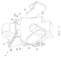
- FIG. 7 is a perspective view of the electrical connector 2 ′ of another embodiment of the present application.
- FIG. 8 is another perspective view of the electrical connector 2 ′ of another embodiment of the present application.
- the electrical connector 2 ′ is similar to the electrical connector 2 , the main difference is that other conductive traces are formed on the housing 21 of the electrical connector 2 ′.
- the electrical connector 2 ′ comprises second conductive traces 26 , 27 , wherein the second conductive traces 26 , 27 extend on the lower stepped face 214 a , the higher stepped face 214 b and the connection face 217 .
- An end portion 262 or end portion 272 of the each second conductive trace 26 or second conductive trace 27 extends to be adjacent to the end portions 242 , 252 of the first conductive traces 24 , 25 for electrically connecting the circuit board 3 ; and the other end portion 261 or end portion 271 of the each second conductive trace 26 or second conductive trace 27 is formed on the higher stepped face 214 b for electrically connecting another electronic device (not shown).
- the other end portion 261 or end portion 271 may comprise a round connection pad.
- the housing 21 has a front surface 210 and an end face 220 .
- the front surface 210 is between the end face 220 and the front surface 213
- the end face 220 is between the front surface 210 and the lower stepped face 214 a .
- the electrical connector 2 ′ may further comprise a third conductive trace 28 or third conductive trace 29 , the third conductive trace 28 or third conductive trace 29 extends on the front surface 210 , the end face 220 and the lower stepped face 214 a .
- An end portion 281 or end portion 291 of the third conductive trace 28 or third conductive trace 29 extends onto the front surface 210 for electrically connecting another electronic device (not shown), and the other end portion 282 or end portion 292 is positioned on the lower stepped face 214 a near the end portions 242 , 252 of the first conductive trace 24 , 25 for electrically connecting the circuit board 3 .
- the end portion 242 or end portion 252 of the first conductive trace 24 or first conductive trace 25 , the end portion 262 or end portion 272 of the second conductive trace 26 or second conductive trace 27 or the end portion 282 or end portion 292 of the third conductive trace 28 or third conductive trace 29 may be fixed on the circuit board together by using the surface mount technology.
- the electrical connector as depicted includes the housing, the terminal and the conductive trace.
- An end portion of the conductive trace may be connected to the electronic device or the circuit board.
- the terminal is connected to the electronic device or the circuit board via the conductive trace, thus the terminal can be shorter and has simple structure, which improves manufacturing.
- the conductive trace replaces the portion of the terminal assembled or embedded in the housing in the prior art, and the conductive trace is formed on the surface of the housing to reduce the volume of the housing, so as to facilitate application of the electrical connector in thin type devices.
Abstract
Description
Claims (12)
Applications Claiming Priority (3)
| Application Number | Priority Date | Filing Date | Title |
|---|---|---|---|
| CN201220401958U | 2012-08-14 | ||
| CN201220401958.8 | 2012-08-14 | ||
| CN201220401958.8U CN202840021U (en) | 2012-08-14 | 2012-08-14 | Electrical connector |
Publications (2)
| Publication Number | Publication Date |
|---|---|
| US20140051284A1 US20140051284A1 (en) | 2014-02-20 |
| US9059544B2 true US9059544B2 (en) | 2015-06-16 |
Family
ID=47951644
Family Applications (1)
| Application Number | Title | Priority Date | Filing Date |
|---|---|---|---|
| US13/963,133 Expired - Fee Related US9059544B2 (en) | 2012-08-14 | 2013-08-09 | Electrical connector |
Country Status (3)
| Country | Link |
|---|---|
| US (1) | US9059544B2 (en) |
| CN (1) | CN202840021U (en) |
| TW (1) | TWM449400U (en) |
Families Citing this family (1)
| Publication number | Priority date | Publication date | Assignee | Title |
|---|---|---|---|---|
| KR20170058742A (en) * | 2015-11-19 | 2017-05-29 | 현대자동차주식회사 | Touch control device, vehicle comprising the same, and manufacturing method thereof |
Citations (41)
| Publication number | Priority date | Publication date | Assignee | Title |
|---|---|---|---|---|
| US1641513A (en) * | 1925-05-06 | 1927-09-06 | Dubillier Condenser Corp | Supporting means for electrical devices |
| US2352576A (en) * | 1940-12-31 | 1944-06-27 | Ray L Triplett | Battery clip |
| US3392365A (en) * | 1962-01-12 | 1968-07-09 | Sperry Rand Corp | Battery holder and contact assembly |
| US3629793A (en) * | 1968-09-25 | 1971-12-21 | Eastman Kodak Co | Battery compartment |
| US3993395A (en) * | 1975-01-06 | 1976-11-23 | Taylor Industries, Inc. | Modular snap-together fuse block assembly |
| US4082408A (en) * | 1977-02-24 | 1978-04-04 | Gould, Inc. | Electric fuse holder |
| US4586777A (en) * | 1984-07-16 | 1986-05-06 | Lucerne Products, Inc. | Battery-switch module adapter |
| US4606590A (en) * | 1984-02-24 | 1986-08-19 | Schurter Ag | Fuse holder clip and clip-type fuse holder for selectively holding different electrical fuses |
| US4607904A (en) * | 1984-08-27 | 1986-08-26 | Duracell Inc. | Battery terminal connector and handle |
| US4699445A (en) * | 1986-07-28 | 1987-10-13 | Amp Incorporated | Electrical terminal assembly for thermistors |
| US4872262A (en) * | 1988-08-15 | 1989-10-10 | Cooper Industries, Inc. | Holder for a blade-type circuit element |
| US4938708A (en) * | 1989-06-23 | 1990-07-03 | United Technologies Automotive, Inc. | Mounting arrangement for cartridge bulb and improved terminal therefor |
| US4938709A (en) * | 1989-06-19 | 1990-07-03 | Judco Manufacturing Corporation | Connection terminals for rigid-wire loop cartridge light bulbs |
| US4995819A (en) * | 1988-06-03 | 1991-02-26 | Amp Incorporated | Set of strips of electrical terminals and a method of loading an electrical connector with said terminals |
| US5007844A (en) * | 1990-01-17 | 1991-04-16 | Hewlett-Packard Company | Surface mount method and device |
| US5108314A (en) * | 1990-04-25 | 1992-04-28 | Daiichi Denso Buhin Co., Ltd. | Connector assembly for electrical components |
| US5186652A (en) * | 1991-10-21 | 1993-02-16 | Hai Yung Ku | Self-power-contained multipurpose plug socket |
| US5288249A (en) * | 1992-09-02 | 1994-02-22 | Cooper Industries, Inc. | Base for cartridge lamp |
| US5395263A (en) * | 1993-03-24 | 1995-03-07 | C & K Systems, Inc. | Dual battery holder |
| US5484297A (en) * | 1993-09-27 | 1996-01-16 | Yazaki Corporation | Lever fitting-type connector |
| US5586891A (en) * | 1994-05-04 | 1996-12-24 | Electronic Designs Inc. | Electrical socket for high-frequency applications |
| US5590058A (en) * | 1991-04-29 | 1996-12-31 | Trw Inc. | Battery monitor for unobstrusive installation with a battery connector |
| US5736271A (en) * | 1996-06-28 | 1998-04-07 | Telxon Corporation | Battery pack for portable electronic device |
| US5808859A (en) * | 1996-12-20 | 1998-09-15 | Liang; Shih-Tsung | Circuit breaker box |
| US5957731A (en) * | 1995-02-26 | 1999-09-28 | Moriyama Sangyo Kabushiki Kaisha | Socket and socket holder for capless incandescent lamp |
| US6007351A (en) * | 1998-07-23 | 1999-12-28 | Packard Hughes Interconnect Company | Bussplate |
| US6149470A (en) * | 1999-02-26 | 2000-11-21 | Berg Technology, Inc. | Electrical connector for antenna or the like |
| US6231370B1 (en) * | 1998-03-19 | 2001-05-15 | The Whitaker Corporation | Electrical connector for leaded electronic component |
| US6375494B2 (en) * | 2000-01-25 | 2002-04-23 | Telefonaktiebolaget Lm Ericsson (Publ) | Metal component carrier |
| US6530804B1 (en) * | 2002-04-11 | 2003-03-11 | Hon Hai Precision Ind. Co., Ltd. | Battery holder |
| US6579119B1 (en) * | 2002-05-03 | 2003-06-17 | Hon Hai Precision Ind. Co., Ltd. | Battery holder |
| US6623293B1 (en) * | 2002-04-03 | 2003-09-23 | Hon Hai Precision Ind. Co., Ltd. | Battery holder having means for securely retaining battery in position |
| US6634891B1 (en) * | 2002-06-11 | 2003-10-21 | Hon Hai Precision Ind. Co., Ltd. | Reworking device for removing electrical elements mounted on motherboard |
| US6692315B1 (en) * | 1999-06-17 | 2004-02-17 | Ferraz Shawmut | Fuse holder and fuse holder clip |
| US6762375B2 (en) * | 2002-05-07 | 2004-07-13 | Phonak Ag | On/off switching device for an electric apparatus or component |
| US6843690B2 (en) | 2002-04-02 | 2005-01-18 | Siemens Audiologische Technik Gmbh | Contact device for hearing aids |
| US7530850B2 (en) * | 2004-07-23 | 2009-05-12 | Ford Global Technologies, Llc | Circuit disconnect assembly |
| US7564337B2 (en) * | 2005-03-03 | 2009-07-21 | Littelfuse, Inc. | Thermally decoupling fuse holder and assembly |
| US7575487B2 (en) * | 2007-06-07 | 2009-08-18 | Yokowo Co., Ltd. | Electric connector |
| US7710236B2 (en) * | 2006-08-01 | 2010-05-04 | Delphi Technologies, Inc. | Fuse systems with serviceable connections |
| US7782010B2 (en) | 2006-06-08 | 2010-08-24 | Siemens Audiologische Technik Gmbh | SMD battery contact module |
-
2012
- 2012-08-14 CN CN201220401958.8U patent/CN202840021U/en not_active Expired - Fee Related
- 2012-09-18 TW TW101217988U patent/TWM449400U/en not_active IP Right Cessation
-
2013
- 2013-08-09 US US13/963,133 patent/US9059544B2/en not_active Expired - Fee Related
Patent Citations (41)
| Publication number | Priority date | Publication date | Assignee | Title |
|---|---|---|---|---|
| US1641513A (en) * | 1925-05-06 | 1927-09-06 | Dubillier Condenser Corp | Supporting means for electrical devices |
| US2352576A (en) * | 1940-12-31 | 1944-06-27 | Ray L Triplett | Battery clip |
| US3392365A (en) * | 1962-01-12 | 1968-07-09 | Sperry Rand Corp | Battery holder and contact assembly |
| US3629793A (en) * | 1968-09-25 | 1971-12-21 | Eastman Kodak Co | Battery compartment |
| US3993395A (en) * | 1975-01-06 | 1976-11-23 | Taylor Industries, Inc. | Modular snap-together fuse block assembly |
| US4082408A (en) * | 1977-02-24 | 1978-04-04 | Gould, Inc. | Electric fuse holder |
| US4606590A (en) * | 1984-02-24 | 1986-08-19 | Schurter Ag | Fuse holder clip and clip-type fuse holder for selectively holding different electrical fuses |
| US4586777A (en) * | 1984-07-16 | 1986-05-06 | Lucerne Products, Inc. | Battery-switch module adapter |
| US4607904A (en) * | 1984-08-27 | 1986-08-26 | Duracell Inc. | Battery terminal connector and handle |
| US4699445A (en) * | 1986-07-28 | 1987-10-13 | Amp Incorporated | Electrical terminal assembly for thermistors |
| US4995819A (en) * | 1988-06-03 | 1991-02-26 | Amp Incorporated | Set of strips of electrical terminals and a method of loading an electrical connector with said terminals |
| US4872262A (en) * | 1988-08-15 | 1989-10-10 | Cooper Industries, Inc. | Holder for a blade-type circuit element |
| US4938709A (en) * | 1989-06-19 | 1990-07-03 | Judco Manufacturing Corporation | Connection terminals for rigid-wire loop cartridge light bulbs |
| US4938708A (en) * | 1989-06-23 | 1990-07-03 | United Technologies Automotive, Inc. | Mounting arrangement for cartridge bulb and improved terminal therefor |
| US5007844A (en) * | 1990-01-17 | 1991-04-16 | Hewlett-Packard Company | Surface mount method and device |
| US5108314A (en) * | 1990-04-25 | 1992-04-28 | Daiichi Denso Buhin Co., Ltd. | Connector assembly for electrical components |
| US5590058A (en) * | 1991-04-29 | 1996-12-31 | Trw Inc. | Battery monitor for unobstrusive installation with a battery connector |
| US5186652A (en) * | 1991-10-21 | 1993-02-16 | Hai Yung Ku | Self-power-contained multipurpose plug socket |
| US5288249A (en) * | 1992-09-02 | 1994-02-22 | Cooper Industries, Inc. | Base for cartridge lamp |
| US5395263A (en) * | 1993-03-24 | 1995-03-07 | C & K Systems, Inc. | Dual battery holder |
| US5484297A (en) * | 1993-09-27 | 1996-01-16 | Yazaki Corporation | Lever fitting-type connector |
| US5586891A (en) * | 1994-05-04 | 1996-12-24 | Electronic Designs Inc. | Electrical socket for high-frequency applications |
| US5957731A (en) * | 1995-02-26 | 1999-09-28 | Moriyama Sangyo Kabushiki Kaisha | Socket and socket holder for capless incandescent lamp |
| US5736271A (en) * | 1996-06-28 | 1998-04-07 | Telxon Corporation | Battery pack for portable electronic device |
| US5808859A (en) * | 1996-12-20 | 1998-09-15 | Liang; Shih-Tsung | Circuit breaker box |
| US6231370B1 (en) * | 1998-03-19 | 2001-05-15 | The Whitaker Corporation | Electrical connector for leaded electronic component |
| US6007351A (en) * | 1998-07-23 | 1999-12-28 | Packard Hughes Interconnect Company | Bussplate |
| US6149470A (en) * | 1999-02-26 | 2000-11-21 | Berg Technology, Inc. | Electrical connector for antenna or the like |
| US6692315B1 (en) * | 1999-06-17 | 2004-02-17 | Ferraz Shawmut | Fuse holder and fuse holder clip |
| US6375494B2 (en) * | 2000-01-25 | 2002-04-23 | Telefonaktiebolaget Lm Ericsson (Publ) | Metal component carrier |
| US6843690B2 (en) | 2002-04-02 | 2005-01-18 | Siemens Audiologische Technik Gmbh | Contact device for hearing aids |
| US6623293B1 (en) * | 2002-04-03 | 2003-09-23 | Hon Hai Precision Ind. Co., Ltd. | Battery holder having means for securely retaining battery in position |
| US6530804B1 (en) * | 2002-04-11 | 2003-03-11 | Hon Hai Precision Ind. Co., Ltd. | Battery holder |
| US6579119B1 (en) * | 2002-05-03 | 2003-06-17 | Hon Hai Precision Ind. Co., Ltd. | Battery holder |
| US6762375B2 (en) * | 2002-05-07 | 2004-07-13 | Phonak Ag | On/off switching device for an electric apparatus or component |
| US6634891B1 (en) * | 2002-06-11 | 2003-10-21 | Hon Hai Precision Ind. Co., Ltd. | Reworking device for removing electrical elements mounted on motherboard |
| US7530850B2 (en) * | 2004-07-23 | 2009-05-12 | Ford Global Technologies, Llc | Circuit disconnect assembly |
| US7564337B2 (en) * | 2005-03-03 | 2009-07-21 | Littelfuse, Inc. | Thermally decoupling fuse holder and assembly |
| US7782010B2 (en) | 2006-06-08 | 2010-08-24 | Siemens Audiologische Technik Gmbh | SMD battery contact module |
| US7710236B2 (en) * | 2006-08-01 | 2010-05-04 | Delphi Technologies, Inc. | Fuse systems with serviceable connections |
| US7575487B2 (en) * | 2007-06-07 | 2009-08-18 | Yokowo Co., Ltd. | Electric connector |
Also Published As
| Publication number | Publication date |
|---|---|
| CN202840021U (en) | 2013-03-27 |
| US20140051284A1 (en) | 2014-02-20 |
| TWM449400U (en) | 2013-03-21 |
Similar Documents
| Publication | Publication Date | Title |
|---|---|---|
| KR101610228B1 (en) | Method for manufacturing receptacle connector | |
| TWI495200B (en) | Electrical connector | |
| US8821191B2 (en) | Electrical connector assembly | |
| CN208062301U (en) | Conducting terminal and its electric connector | |
| US20140080327A1 (en) | Shielding socket with a shielding plate extending outside from an insulative housing | |
| TW200303633A (en) | Surface-mounted right-angle electrical connector | |
| US9039453B2 (en) | Electrical connector | |
| JP2009218455A5 (en) | ||
| US9059544B2 (en) | Electrical connector | |
| TWM569091U (en) | Quick assembly type stable USB TYPE-C connector | |
| US20150311622A1 (en) | Connector shell used in a lightning connector | |
| US8292632B2 (en) | Compression connector with sink board-mounting structure | |
| US9437960B2 (en) | Dustproof cover for charging port of electronic device and charging base corresponding to dustproof cover | |
| SG176336A1 (en) | Sim card connector and sim card connector assembly including the same | |
| KR101593585B1 (en) | PCB having connector of direct contact LCD module | |
| CN109524827B (en) | Socket connector | |
| US7476109B2 (en) | Electrical connector assembled with a bondable element | |
| TW201505269A (en) | Electrical connector and assembly thereof | |
| TW200952267A (en) | Electrical connector | |
| JP2018055851A (en) | connector | |
| CN104795653B (en) | Electric connector | |
| TWI573355B (en) | Electrical connector | |
| TWI735130B (en) | Connector and connector processing method | |
| US20140291002A1 (en) | Printed circuit board module | |
| JP2017016843A (en) | connector |
Legal Events
| Date | Code | Title | Description |
|---|---|---|---|
| AS | Assignment |
Owner name: MOLEX INCORPORATED, ILLINOIS Free format text: ASSIGNMENT OF ASSIGNORS INTEREST;ASSIGNOR:SONG, XIAO JUN;REEL/FRAME:031356/0342 Effective date: 20130826 |
|
| STCF | Information on status: patent grant |
Free format text: PATENTED CASE |
|
| MAFP | Maintenance fee payment |
Free format text: PAYMENT OF MAINTENANCE FEE, 4TH YEAR, LARGE ENTITY (ORIGINAL EVENT CODE: M1551); ENTITY STATUS OF PATENT OWNER: LARGE ENTITY Year of fee payment: 4 |
|
| FEPP | Fee payment procedure |
Free format text: MAINTENANCE FEE REMINDER MAILED (ORIGINAL EVENT CODE: REM.); ENTITY STATUS OF PATENT OWNER: LARGE ENTITY |
|
| LAPS | Lapse for failure to pay maintenance fees |
Free format text: PATENT EXPIRED FOR FAILURE TO PAY MAINTENANCE FEES (ORIGINAL EVENT CODE: EXP.); ENTITY STATUS OF PATENT OWNER: LARGE ENTITY |
|
| STCH | Information on status: patent discontinuation |
Free format text: PATENT EXPIRED DUE TO NONPAYMENT OF MAINTENANCE FEES UNDER 37 CFR 1.362 |
|
| FP | Lapsed due to failure to pay maintenance fee |
Effective date: 20230616 |