US9059286B2 - Pre-gate, source/drain strain layer formation - Google Patents
Pre-gate, source/drain strain layer formation Download PDFInfo
- Publication number
- US9059286B2 US9059286B2 US14/230,087 US201414230087A US9059286B2 US 9059286 B2 US9059286 B2 US 9059286B2 US 201414230087 A US201414230087 A US 201414230087A US 9059286 B2 US9059286 B2 US 9059286B2
- Authority
- US
- United States
- Prior art keywords
- strain
- layer
- channel region
- forming
- producing
- Prior art date
- Legal status (The legal status is an assumption and is not a legal conclusion. Google has not performed a legal analysis and makes no representation as to the accuracy of the status listed.)
- Expired - Fee Related, expires
Links
- 230000015572 biosynthetic process Effects 0.000 title 1
- 238000000034 method Methods 0.000 claims abstract description 60
- 239000012212 insulator Substances 0.000 claims abstract description 39
- 239000004020 conductor Substances 0.000 claims abstract description 24
- 239000000758 substrate Substances 0.000 claims abstract description 14
- 238000002955 isolation Methods 0.000 claims description 15
- 229910000577 Silicon-germanium Inorganic materials 0.000 claims description 8
- 239000004065 semiconductor Substances 0.000 claims description 5
- 230000008569 process Effects 0.000 description 20
- 239000012535 impurity Substances 0.000 description 15
- 239000000463 material Substances 0.000 description 15
- XUIMIQQOPSSXEZ-UHFFFAOYSA-N Silicon Chemical group [Si] XUIMIQQOPSSXEZ-UHFFFAOYSA-N 0.000 description 12
- 229910052710 silicon Inorganic materials 0.000 description 12
- 239000010703 silicon Substances 0.000 description 12
- 238000004519 manufacturing process Methods 0.000 description 11
- 238000010586 diagram Methods 0.000 description 10
- 125000006850 spacer group Chemical group 0.000 description 9
- 239000002210 silicon-based material Substances 0.000 description 5
- 239000003989 dielectric material Substances 0.000 description 3
- 229910052732 germanium Inorganic materials 0.000 description 3
- 239000011810 insulating material Substances 0.000 description 3
- 229910021420 polycrystalline silicon Inorganic materials 0.000 description 3
- 239000000126 substance Substances 0.000 description 3
- OKTJSMMVPCPJKN-UHFFFAOYSA-N Carbon Chemical compound [C] OKTJSMMVPCPJKN-UHFFFAOYSA-N 0.000 description 2
- PXHVJJICTQNCMI-UHFFFAOYSA-N Nickel Chemical compound [Ni] PXHVJJICTQNCMI-UHFFFAOYSA-N 0.000 description 2
- 229910052581 Si3N4 Inorganic materials 0.000 description 2
- VYPSYNLAJGMNEJ-UHFFFAOYSA-N Silicium dioxide Chemical compound O=[Si]=O VYPSYNLAJGMNEJ-UHFFFAOYSA-N 0.000 description 2
- 229910021417 amorphous silicon Inorganic materials 0.000 description 2
- 230000008901 benefit Effects 0.000 description 2
- 229910052799 carbon Inorganic materials 0.000 description 2
- 230000008859 change Effects 0.000 description 2
- 239000007795 chemical reaction product Substances 0.000 description 2
- 230000002708 enhancing effect Effects 0.000 description 2
- 230000005669 field effect Effects 0.000 description 2
- GNPVGFCGXDBREM-UHFFFAOYSA-N germanium atom Chemical compound [Ge] GNPVGFCGXDBREM-UHFFFAOYSA-N 0.000 description 2
- 230000001965 increasing effect Effects 0.000 description 2
- 230000010354 integration Effects 0.000 description 2
- 229910052751 metal Inorganic materials 0.000 description 2
- 239000002184 metal Substances 0.000 description 2
- 239000000203 mixture Substances 0.000 description 2
- 238000012986 modification Methods 0.000 description 2
- 230000004048 modification Effects 0.000 description 2
- 238000001020 plasma etching Methods 0.000 description 2
- 229920005591 polysilicon Polymers 0.000 description 2
- 239000000047 product Substances 0.000 description 2
- ZOXJGFHDIHLPTG-UHFFFAOYSA-N Boron Chemical compound [B] ZOXJGFHDIHLPTG-UHFFFAOYSA-N 0.000 description 1
- 229910001218 Gallium arsenide Inorganic materials 0.000 description 1
- 229910000927 Ge alloy Inorganic materials 0.000 description 1
- 229910000673 Indium arsenide Inorganic materials 0.000 description 1
- ZOKXTWBITQBERF-UHFFFAOYSA-N Molybdenum Chemical compound [Mo] ZOKXTWBITQBERF-UHFFFAOYSA-N 0.000 description 1
- OAICVXFJPJFONN-UHFFFAOYSA-N Phosphorus Chemical compound [P] OAICVXFJPJFONN-UHFFFAOYSA-N 0.000 description 1
- 229910003811 SiGeC Inorganic materials 0.000 description 1
- RTAQQCXQSZGOHL-UHFFFAOYSA-N Titanium Chemical compound [Ti] RTAQQCXQSZGOHL-UHFFFAOYSA-N 0.000 description 1
- HMDDXIMCDZRSNE-UHFFFAOYSA-N [C].[Si] Chemical compound [C].[Si] HMDDXIMCDZRSNE-UHFFFAOYSA-N 0.000 description 1
- LEVVHYCKPQWKOP-UHFFFAOYSA-N [Si].[Ge] Chemical compound [Si].[Ge] LEVVHYCKPQWKOP-UHFFFAOYSA-N 0.000 description 1
- 229910052787 antimony Inorganic materials 0.000 description 1
- WATWJIUSRGPENY-UHFFFAOYSA-N antimony atom Chemical compound [Sb] WATWJIUSRGPENY-UHFFFAOYSA-N 0.000 description 1
- 229910052785 arsenic Inorganic materials 0.000 description 1
- RQNWIZPPADIBDY-UHFFFAOYSA-N arsenic atom Chemical compound [As] RQNWIZPPADIBDY-UHFFFAOYSA-N 0.000 description 1
- QVGXLLKOCUKJST-UHFFFAOYSA-N atomic oxygen Chemical compound [O] QVGXLLKOCUKJST-UHFFFAOYSA-N 0.000 description 1
- 230000004888 barrier function Effects 0.000 description 1
- 229910052796 boron Inorganic materials 0.000 description 1
- 239000000919 ceramic Substances 0.000 description 1
- 229910010293 ceramic material Inorganic materials 0.000 description 1
- 238000005229 chemical vapour deposition Methods 0.000 description 1
- 229910052681 coesite Inorganic materials 0.000 description 1
- 150000001875 compounds Chemical class 0.000 description 1
- 230000006835 compression Effects 0.000 description 1
- 238000007906 compression Methods 0.000 description 1
- 229910052906 cristobalite Inorganic materials 0.000 description 1
- 230000003247 decreasing effect Effects 0.000 description 1
- 230000001419 dependent effect Effects 0.000 description 1
- 238000000151 deposition Methods 0.000 description 1
- 238000009792 diffusion process Methods 0.000 description 1
- 239000002019 doping agent Substances 0.000 description 1
- -1 e.g. Substances 0.000 description 1
- 238000005530 etching Methods 0.000 description 1
- 229910052735 hafnium Inorganic materials 0.000 description 1
- VBJZVLUMGGDVMO-UHFFFAOYSA-N hafnium atom Chemical compound [Hf] VBJZVLUMGGDVMO-UHFFFAOYSA-N 0.000 description 1
- 229910052738 indium Inorganic materials 0.000 description 1
- RPQDHPTXJYYUPQ-UHFFFAOYSA-N indium arsenide Chemical compound [In]#[As] RPQDHPTXJYYUPQ-UHFFFAOYSA-N 0.000 description 1
- APFVFJFRJDLVQX-UHFFFAOYSA-N indium atom Chemical compound [In] APFVFJFRJDLVQX-UHFFFAOYSA-N 0.000 description 1
- 239000013067 intermediate product Substances 0.000 description 1
- 229910044991 metal oxide Inorganic materials 0.000 description 1
- 150000004706 metal oxides Chemical class 0.000 description 1
- 150000002739 metals Chemical class 0.000 description 1
- 229910003465 moissanite Inorganic materials 0.000 description 1
- 229910052750 molybdenum Inorganic materials 0.000 description 1
- 239000011733 molybdenum Substances 0.000 description 1
- 229910052759 nickel Inorganic materials 0.000 description 1
- 229910052760 oxygen Inorganic materials 0.000 description 1
- 239000001301 oxygen Substances 0.000 description 1
- BPUBBGLMJRNUCC-UHFFFAOYSA-N oxygen(2-);tantalum(5+) Chemical compound [O-2].[O-2].[O-2].[O-2].[O-2].[Ta+5].[Ta+5] BPUBBGLMJRNUCC-UHFFFAOYSA-N 0.000 description 1
- 238000000059 patterning Methods 0.000 description 1
- 229910052698 phosphorus Inorganic materials 0.000 description 1
- 239000011574 phosphorus Substances 0.000 description 1
- 238000005240 physical vapour deposition Methods 0.000 description 1
- 238000005498 polishing Methods 0.000 description 1
- 229910021332 silicide Inorganic materials 0.000 description 1
- FVBUAEGBCNSCDD-UHFFFAOYSA-N silicide(4-) Chemical compound [Si-4] FVBUAEGBCNSCDD-UHFFFAOYSA-N 0.000 description 1
- 229910010271 silicon carbide Inorganic materials 0.000 description 1
- 239000000377 silicon dioxide Substances 0.000 description 1
- HQVNEWCFYHHQES-UHFFFAOYSA-N silicon nitride Chemical compound N12[Si]34N5[Si]62N3[Si]51N64 HQVNEWCFYHHQES-UHFFFAOYSA-N 0.000 description 1
- 229910052682 stishovite Inorganic materials 0.000 description 1
- 229910052715 tantalum Inorganic materials 0.000 description 1
- GUVRBAGPIYLISA-UHFFFAOYSA-N tantalum atom Chemical compound [Ta] GUVRBAGPIYLISA-UHFFFAOYSA-N 0.000 description 1
- 229910001936 tantalum oxide Inorganic materials 0.000 description 1
- 239000010936 titanium Substances 0.000 description 1
- 229910052719 titanium Inorganic materials 0.000 description 1
- 229910052905 tridymite Inorganic materials 0.000 description 1
- WFKWXMTUELFFGS-UHFFFAOYSA-N tungsten Chemical compound [W] WFKWXMTUELFFGS-UHFFFAOYSA-N 0.000 description 1
- 229910052721 tungsten Inorganic materials 0.000 description 1
- 239000010937 tungsten Substances 0.000 description 1
Images


Classifications
-
- H—ELECTRICITY
- H01—ELECTRIC ELEMENTS
- H01L—SEMICONDUCTOR DEVICES NOT COVERED BY CLASS H10
- H01L29/00—Semiconductor devices adapted for rectifying, amplifying, oscillating or switching, or capacitors or resistors with at least one potential-jump barrier or surface barrier, e.g. PN junction depletion layer or carrier concentration layer; Details of semiconductor bodies or of electrodes thereof ; Multistep manufacturing processes therefor
- H01L29/02—Semiconductor bodies ; Multistep manufacturing processes therefor
- H01L29/06—Semiconductor bodies ; Multistep manufacturing processes therefor characterised by their shape; characterised by the shapes, relative sizes, or dispositions of the semiconductor regions ; characterised by the concentration or distribution of impurities within semiconductor regions
- H01L29/10—Semiconductor bodies ; Multistep manufacturing processes therefor characterised by their shape; characterised by the shapes, relative sizes, or dispositions of the semiconductor regions ; characterised by the concentration or distribution of impurities within semiconductor regions with semiconductor regions connected to an electrode not carrying current to be rectified, amplified or switched and such electrode being part of a semiconductor device which comprises three or more electrodes
- H01L29/1025—Channel region of field-effect devices
- H01L29/1029—Channel region of field-effect devices of field-effect transistors
- H01L29/1033—Channel region of field-effect devices of field-effect transistors with insulated gate, e.g. characterised by the length, the width, the geometric contour or the doping structure
- H01L29/1054—Channel region of field-effect devices of field-effect transistors with insulated gate, e.g. characterised by the length, the width, the geometric contour or the doping structure with a variation of the composition, e.g. channel with strained layer for increasing the mobility
-
- H—ELECTRICITY
- H01—ELECTRIC ELEMENTS
- H01L—SEMICONDUCTOR DEVICES NOT COVERED BY CLASS H10
- H01L29/00—Semiconductor devices adapted for rectifying, amplifying, oscillating or switching, or capacitors or resistors with at least one potential-jump barrier or surface barrier, e.g. PN junction depletion layer or carrier concentration layer; Details of semiconductor bodies or of electrodes thereof ; Multistep manufacturing processes therefor
- H01L29/66—Types of semiconductor device ; Multistep manufacturing processes therefor
- H01L29/68—Types of semiconductor device ; Multistep manufacturing processes therefor controllable by only the electric current supplied, or only the electric potential applied, to an electrode which does not carry the current to be rectified, amplified or switched
- H01L29/76—Unipolar devices, e.g. field effect transistors
- H01L29/772—Field effect transistors
- H01L29/78—Field effect transistors with field effect produced by an insulated gate
- H01L29/7842—Field effect transistors with field effect produced by an insulated gate means for exerting mechanical stress on the crystal lattice of the channel region, e.g. using a flexible substrate
- H01L29/7848—Field effect transistors with field effect produced by an insulated gate means for exerting mechanical stress on the crystal lattice of the channel region, e.g. using a flexible substrate the means being located in the source/drain region, e.g. SiGe source and drain
-
- H—ELECTRICITY
- H01—ELECTRIC ELEMENTS
- H01L—SEMICONDUCTOR DEVICES NOT COVERED BY CLASS H10
- H01L21/00—Processes or apparatus adapted for the manufacture or treatment of semiconductor or solid state devices or of parts thereof
- H01L21/70—Manufacture or treatment of devices consisting of a plurality of solid state components formed in or on a common substrate or of parts thereof; Manufacture of integrated circuit devices or of parts thereof
- H01L21/77—Manufacture or treatment of devices consisting of a plurality of solid state components or integrated circuits formed in, or on, a common substrate
- H01L21/78—Manufacture or treatment of devices consisting of a plurality of solid state components or integrated circuits formed in, or on, a common substrate with subsequent division of the substrate into plural individual devices
- H01L21/82—Manufacture or treatment of devices consisting of a plurality of solid state components or integrated circuits formed in, or on, a common substrate with subsequent division of the substrate into plural individual devices to produce devices, e.g. integrated circuits, each consisting of a plurality of components
- H01L21/822—Manufacture or treatment of devices consisting of a plurality of solid state components or integrated circuits formed in, or on, a common substrate with subsequent division of the substrate into plural individual devices to produce devices, e.g. integrated circuits, each consisting of a plurality of components the substrate being a semiconductor, using silicon technology
- H01L21/8232—Field-effect technology
- H01L21/8234—MIS technology, i.e. integration processes of field effect transistors of the conductor-insulator-semiconductor type
- H01L21/823412—MIS technology, i.e. integration processes of field effect transistors of the conductor-insulator-semiconductor type with a particular manufacturing method of the channel structures, e.g. channel implants, halo or pocket implants, or channel materials
-
- H—ELECTRICITY
- H01—ELECTRIC ELEMENTS
- H01L—SEMICONDUCTOR DEVICES NOT COVERED BY CLASS H10
- H01L21/00—Processes or apparatus adapted for the manufacture or treatment of semiconductor or solid state devices or of parts thereof
- H01L21/70—Manufacture or treatment of devices consisting of a plurality of solid state components formed in or on a common substrate or of parts thereof; Manufacture of integrated circuit devices or of parts thereof
- H01L21/77—Manufacture or treatment of devices consisting of a plurality of solid state components or integrated circuits formed in, or on, a common substrate
- H01L21/78—Manufacture or treatment of devices consisting of a plurality of solid state components or integrated circuits formed in, or on, a common substrate with subsequent division of the substrate into plural individual devices
- H01L21/82—Manufacture or treatment of devices consisting of a plurality of solid state components or integrated circuits formed in, or on, a common substrate with subsequent division of the substrate into plural individual devices to produce devices, e.g. integrated circuits, each consisting of a plurality of components
- H01L21/822—Manufacture or treatment of devices consisting of a plurality of solid state components or integrated circuits formed in, or on, a common substrate with subsequent division of the substrate into plural individual devices to produce devices, e.g. integrated circuits, each consisting of a plurality of components the substrate being a semiconductor, using silicon technology
- H01L21/8232—Field-effect technology
- H01L21/8234—MIS technology, i.e. integration processes of field effect transistors of the conductor-insulator-semiconductor type
- H01L21/8238—Complementary field-effect transistors, e.g. CMOS
- H01L21/823807—Complementary field-effect transistors, e.g. CMOS with a particular manufacturing method of the channel structures, e.g. channel implants, halo or pocket implants, or channel materials
-
- H—ELECTRICITY
- H01—ELECTRIC ELEMENTS
- H01L—SEMICONDUCTOR DEVICES NOT COVERED BY CLASS H10
- H01L29/00—Semiconductor devices adapted for rectifying, amplifying, oscillating or switching, or capacitors or resistors with at least one potential-jump barrier or surface barrier, e.g. PN junction depletion layer or carrier concentration layer; Details of semiconductor bodies or of electrodes thereof ; Multistep manufacturing processes therefor
- H01L29/02—Semiconductor bodies ; Multistep manufacturing processes therefor
- H01L29/12—Semiconductor bodies ; Multistep manufacturing processes therefor characterised by the materials of which they are formed
- H01L29/16—Semiconductor bodies ; Multistep manufacturing processes therefor characterised by the materials of which they are formed including, apart from doping materials or other impurities, only elements of Group IV of the Periodic System
- H01L29/161—Semiconductor bodies ; Multistep manufacturing processes therefor characterised by the materials of which they are formed including, apart from doping materials or other impurities, only elements of Group IV of the Periodic System including two or more of the elements provided for in group H01L29/16, e.g. alloys
- H01L29/165—Semiconductor bodies ; Multistep manufacturing processes therefor characterised by the materials of which they are formed including, apart from doping materials or other impurities, only elements of Group IV of the Periodic System including two or more of the elements provided for in group H01L29/16, e.g. alloys in different semiconductor regions, e.g. heterojunctions
-
- H—ELECTRICITY
- H01—ELECTRIC ELEMENTS
- H01L—SEMICONDUCTOR DEVICES NOT COVERED BY CLASS H10
- H01L29/00—Semiconductor devices adapted for rectifying, amplifying, oscillating or switching, or capacitors or resistors with at least one potential-jump barrier or surface barrier, e.g. PN junction depletion layer or carrier concentration layer; Details of semiconductor bodies or of electrodes thereof ; Multistep manufacturing processes therefor
- H01L29/66—Types of semiconductor device ; Multistep manufacturing processes therefor
- H01L29/66007—Multistep manufacturing processes
- H01L29/66075—Multistep manufacturing processes of devices having semiconductor bodies comprising group 14 or group 13/15 materials
- H01L29/66227—Multistep manufacturing processes of devices having semiconductor bodies comprising group 14 or group 13/15 materials the devices being controllable only by the electric current supplied or the electric potential applied, to an electrode which does not carry the current to be rectified, amplified or switched, e.g. three-terminal devices
- H01L29/66409—Unipolar field-effect transistors
- H01L29/66477—Unipolar field-effect transistors with an insulated gate, i.e. MISFET
- H01L29/66545—Unipolar field-effect transistors with an insulated gate, i.e. MISFET using a dummy, i.e. replacement gate in a process wherein at least a part of the final gate is self aligned to the dummy gate
-
- H—ELECTRICITY
- H01—ELECTRIC ELEMENTS
- H01L—SEMICONDUCTOR DEVICES NOT COVERED BY CLASS H10
- H01L29/00—Semiconductor devices adapted for rectifying, amplifying, oscillating or switching, or capacitors or resistors with at least one potential-jump barrier or surface barrier, e.g. PN junction depletion layer or carrier concentration layer; Details of semiconductor bodies or of electrodes thereof ; Multistep manufacturing processes therefor
- H01L29/66—Types of semiconductor device ; Multistep manufacturing processes therefor
- H01L29/66007—Multistep manufacturing processes
- H01L29/66075—Multistep manufacturing processes of devices having semiconductor bodies comprising group 14 or group 13/15 materials
- H01L29/66227—Multistep manufacturing processes of devices having semiconductor bodies comprising group 14 or group 13/15 materials the devices being controllable only by the electric current supplied or the electric potential applied, to an electrode which does not carry the current to be rectified, amplified or switched, e.g. three-terminal devices
- H01L29/66409—Unipolar field-effect transistors
- H01L29/66477—Unipolar field-effect transistors with an insulated gate, i.e. MISFET
- H01L29/66568—Lateral single gate silicon transistors
- H01L29/66636—Lateral single gate silicon transistors with source or drain recessed by etching or first recessed by etching and then refilled
-
- H—ELECTRICITY
- H01—ELECTRIC ELEMENTS
- H01L—SEMICONDUCTOR DEVICES NOT COVERED BY CLASS H10
- H01L29/00—Semiconductor devices adapted for rectifying, amplifying, oscillating or switching, or capacitors or resistors with at least one potential-jump barrier or surface barrier, e.g. PN junction depletion layer or carrier concentration layer; Details of semiconductor bodies or of electrodes thereof ; Multistep manufacturing processes therefor
- H01L29/66—Types of semiconductor device ; Multistep manufacturing processes therefor
- H01L29/66007—Multistep manufacturing processes
- H01L29/66075—Multistep manufacturing processes of devices having semiconductor bodies comprising group 14 or group 13/15 materials
- H01L29/66227—Multistep manufacturing processes of devices having semiconductor bodies comprising group 14 or group 13/15 materials the devices being controllable only by the electric current supplied or the electric potential applied, to an electrode which does not carry the current to be rectified, amplified or switched, e.g. three-terminal devices
- H01L29/66409—Unipolar field-effect transistors
- H01L29/66477—Unipolar field-effect transistors with an insulated gate, i.e. MISFET
- H01L29/66568—Lateral single gate silicon transistors
- H01L29/66651—Lateral single gate silicon transistors with a single crystalline channel formed on the silicon substrate after insulating device isolation
-
- H—ELECTRICITY
- H01—ELECTRIC ELEMENTS
- H01L—SEMICONDUCTOR DEVICES NOT COVERED BY CLASS H10
- H01L29/00—Semiconductor devices adapted for rectifying, amplifying, oscillating or switching, or capacitors or resistors with at least one potential-jump barrier or surface barrier, e.g. PN junction depletion layer or carrier concentration layer; Details of semiconductor bodies or of electrodes thereof ; Multistep manufacturing processes therefor
- H01L29/66—Types of semiconductor device ; Multistep manufacturing processes therefor
- H01L29/68—Types of semiconductor device ; Multistep manufacturing processes therefor controllable by only the electric current supplied, or only the electric potential applied, to an electrode which does not carry the current to be rectified, amplified or switched
- H01L29/76—Unipolar devices, e.g. field effect transistors
- H01L29/772—Field effect transistors
- H01L29/78—Field effect transistors with field effect produced by an insulated gate
- H01L29/7842—Field effect transistors with field effect produced by an insulated gate means for exerting mechanical stress on the crystal lattice of the channel region, e.g. using a flexible substrate
- H01L29/7849—Field effect transistors with field effect produced by an insulated gate means for exerting mechanical stress on the crystal lattice of the channel region, e.g. using a flexible substrate the means being provided under the channel
Definitions
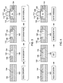
- FIG. 3 is a schematic cross-sectional diagram illustrating multiple stages of an integrated circuit manufacturing process
- the conductors mentioned herein can be formed of any conductive material, such as polycrystalline silicon (polysilicon), amorphous silicon, a combination of amorphous silicon and polysilicon, and polysilicon-germanium, rendered conductive by the presence of a suitable dopant.
- the conductors herein may be one or more metals, such as tungsten, hafnium, tantalum, molybdenum, titanium, or nickel, or a metal silicide, and may be deposited using physical vapor deposition, chemical vapor deposition, or any other technique known in the art.
- Sidewall spacers 110 are structures that are well-known to those ordinarily skilled in the art and are generally formed by depositing or growing a conformal insulating layer (such as any of the insulators mentioned above) and then performing a directional etching process (anisotropic) that etches material from horizontal surfaces at a greater rate than its removes material from vertical surfaces, thereby leaving insulating material along the vertical sidewalls of structures. This material left on the vertical sidewalls is referred to as sidewall spacers 110 .
- recesses 116 are formed in the silicon region 104 by performing any appropriate selective material removal process such as reactive ion etching (RIE).
- RIE reactive ion etching
- the shallow trench isolation regions 102 and the sidewall spacers 110 self-align this material removal process to cause the recesses 116 to be positioned on opposite sides of the channel region of the silicon material 104 .
- source and drain regions 118 can be deposited into the recesses 116 (or grown within the recesses using an epitaxial growth process).
- the source and drain regions 118 comprise of embedded epitaxial stressors, most common known being SiGe for PFET and SiC for NFET.
- Epitaxial growth processes are well-known to those ordinarily skilled in the art and are generally performed by placing the partially formed structure within a chamber that has a high concentration of the material that is to be grown. The combination of temperature and pressure within the chamber allows the material to epitaxially grow upon seed (base) layers of the structure.
- the seed regions are areas of the structure where the material being grown previously exists.
- a silicon material can be epitaxially grown on a base layer of silicon; however, during the epitaxial process, different chemicals and materials can be introduced as impurities to change the chemical makeup of the epitaxially grown material.
- impurities such as those mentioned above
- a stressor impurity such as germanium or carbon, may be introduced into the epitaxial growth process in order to create a material that has a different lattice constant than the base silicon material.
- the process of epitaxially growing the source and drain regions 118 can encounter difficulties relating to misalignment, incomplete growth, non-uniformity of growth, etc. Therefore, the following embodiments form the transistor body after the epitaxial stressor source and drain layer is grown. More specifically, the embodiments herein first grow the stressor layer (e.g., SiGe or SiC), and then form the main body of the device via recess and epitaxial silicon growth.
- the stressor layer e.g., SiGe or SiC
- one method herein produces a transistor.
- the method shown in FIG. 2 patterns STI regions within the silicon base layer 104 , as discussed above.
- the method then recesses the silicon base layer 104 and forms (grows) a strain producing layer 106 within the recess.
- the method shown in FIG. 2 then removes at least one portion of the strain producing layer 106 to create at least one recess 120 in the strain producing layer 106 . This leaves first and second portions of the strain producing layer 106 on the substrate 100 .
- the first and second portions of the strain producing layer 106 comprise source and drain stressor regions 106 of the transistor.
- the method then grows a channel region 122 in the recess 120 of the strain producing layer 106 , forms a gate insulator 108 on the channel region 122 , and forms a gate conductor 112 and sidewall spacers 110 on the gate insulator 108 (after forming the source and drain stressor regions 106 , the channel region 122 , and the gate insulator 108 ).
- the method epitaxially grows the strain producing layer 106 , using processes discussed above.
- the forming of the strain-producing conductive layer can form a layer of SiGe or SiC.
- the method epitaxially grows the channel region 122 .
- the methods herein can form the shallow trench isolation regions 102 either before forming the strain-producing layer ( FIG. 2 ), after forming the strain-producing conductive layer and before removing the portion of the strain-producing layer ( FIG. 3 ), or after the forming of the channel region 122 and before the forming of the gate conductor 112 ( FIG. 4 ).
- the process shown in FIG. 4 eliminates epitaxial facets at the STI edge and allows for a “box shaped” channel region. Note that in all the drawings, the same reference numerals represent the same material, and a redundant discussion of such items is not presented for brevity.
- the gate conductor 112 is considered to be toward the “top” of the structure and the substrate 100 is considered to be toward the “bottom” of the structure.
- vertical it is meant that an item runs straight from the bottom of the structure to the top (e.g., at an approximate 0 degree angle).
- Vertical structures are, therefore, approximately perpendicular (e.g., at an approximate 90 degree angle) to the planar surfaces of the various horizontal layers of the substrate 100 , the gate insulator 108 , the strain-producing layer 106 , etc.
- some embodiments herein can grow a non-uniform channel region in the recess 120 of the strain producing layer 106 .
- the process epitaxially grows a first channel layer 124 (for example SiC) by introducing an impurity during the first part of the epitaxial growth process.
- the process epitaxially grows a second channel layer 122 on the first channel layer, which can consist solely of pure Si or can comprise some different impurity than was used for the first layer 124 .
- FIG. 7 Another non-uniform channel region 126 is shown in FIG. 7 .
- the process alters the doping concentration during the epitaxial growth of the non-uniform channel region 126 .
- the impurity was added to one portion 124 and not added to the other 122 ; in the embodiment shown in FIG. 7 , the concentration of impurity is gradually increased or decreased during the entire epitaxial growth process.
- the methods herein grow the channel region 123 in the recess 120 of the strain producing layer 106 , by forming a multilayer channel 123 in the recess.
- the top (second portion) of the multilayer 123 comprises the transistor channel and is stressed to improve mobility due to lattice mismatch with the first layer underneath. Compression improves PFET mobility, therefore the top layer of the multilayer 123 has a wider lattice constant will be compressed.
- the top layer will be grown to have a smaller lattice constant than the layer beneath (second portion) creating a tensile strain and therefore enhancing electron mobility.
- the embodiments herein provide pre-gate eSiGe integration schemes which form the eSiGe structure using epitaxial growth that is performed before the gate is formed. These processes eliminate the epitaxial fill height-dependent device variability and allow the silicon channel surface to relax, increasing the channel strain and device performance. This also allows negative-proximity P-type field effect transistor (PFET) to produce higher stress. Further, embodiments herein allow the eSiGe vertical composition gradient to be adjusted independently of the horizontal composition gradient, enhancing channel strain.
- PFET negative-proximity P-type field effect transistor
Abstract
Description
Claims (11)
Priority Applications (1)
| Application Number | Priority Date | Filing Date | Title |
|---|---|---|---|
| US14/230,087 US9059286B2 (en) | 2010-03-08 | 2014-03-31 | Pre-gate, source/drain strain layer formation |
Applications Claiming Priority (2)
| Application Number | Priority Date | Filing Date | Title |
|---|---|---|---|
| US12/719,312 US20110215376A1 (en) | 2010-03-08 | 2010-03-08 | Pre-gate, source/drain strain layer formation |
| US14/230,087 US9059286B2 (en) | 2010-03-08 | 2014-03-31 | Pre-gate, source/drain strain layer formation |
Related Parent Applications (1)
| Application Number | Title | Priority Date | Filing Date |
|---|---|---|---|
| US12/719,312 Continuation US20110215376A1 (en) | 2010-03-08 | 2010-03-08 | Pre-gate, source/drain strain layer formation |
Publications (2)
| Publication Number | Publication Date |
|---|---|
| US20140213029A1 US20140213029A1 (en) | 2014-07-31 |
| US9059286B2 true US9059286B2 (en) | 2015-06-16 |
Family
ID=44530554
Family Applications (3)
| Application Number | Title | Priority Date | Filing Date |
|---|---|---|---|
| US12/719,312 Abandoned US20110215376A1 (en) | 2010-03-08 | 2010-03-08 | Pre-gate, source/drain strain layer formation |
| US13/432,018 Abandoned US20120181578A1 (en) | 2010-03-08 | 2012-03-28 | Pre-gate, source/drain strain layer formation |
| US14/230,087 Expired - Fee Related US9059286B2 (en) | 2010-03-08 | 2014-03-31 | Pre-gate, source/drain strain layer formation |
Family Applications Before (2)
| Application Number | Title | Priority Date | Filing Date |
|---|---|---|---|
| US12/719,312 Abandoned US20110215376A1 (en) | 2010-03-08 | 2010-03-08 | Pre-gate, source/drain strain layer formation |
| US13/432,018 Abandoned US20120181578A1 (en) | 2010-03-08 | 2012-03-28 | Pre-gate, source/drain strain layer formation |
Country Status (1)
| Country | Link |
|---|---|
| US (3) | US20110215376A1 (en) |
Cited By (1)
| Publication number | Priority date | Publication date | Assignee | Title |
|---|---|---|---|---|
| US9530886B1 (en) * | 2015-11-27 | 2016-12-27 | United Microelectronics Corp. | Semiconductor device with epitaxial structure and manufacturing method thereof |
Families Citing this family (16)
| Publication number | Priority date | Publication date | Assignee | Title |
|---|---|---|---|---|
| US8426278B2 (en) * | 2010-06-09 | 2013-04-23 | GlobalFoundries, Inc. | Semiconductor devices having stressor regions and related fabrication methods |
| US9006052B2 (en) * | 2010-10-11 | 2015-04-14 | International Business Machines Corporation | Self aligned device with enhanced stress and methods of manufacture |
| US8883583B2 (en) * | 2012-06-26 | 2014-11-11 | Taiwan Semiconductor Manufacturing Company, Ltd. | Semiconductor devices, transistors, and methods of manufacture thereof |
| US8637955B1 (en) * | 2012-08-31 | 2014-01-28 | Suvolta, Inc. | Semiconductor structure with reduced junction leakage and method of fabrication thereof |
| US8946035B2 (en) * | 2012-09-27 | 2015-02-03 | Taiwan Semiconductor Manufacturing Co., Ltd. | Replacement channels for semiconductor devices and methods for forming the same using dopant concentration boost |
| US9972524B2 (en) * | 2013-03-11 | 2018-05-15 | Taiwan Semiconductor Manufacturing Company, Ltd. | Method for fabricating a semiconductor device |
| US9105707B2 (en) * | 2013-07-24 | 2015-08-11 | International Business Machines Corporation | ZRAM heterochannel memory |
| US9224814B2 (en) | 2014-01-16 | 2015-12-29 | Taiwan Semiconductor Manufacturing Co., Ltd. | Process design to improve transistor variations and performance |
| US9236445B2 (en) | 2014-01-16 | 2016-01-12 | Taiwan Semiconductor Manufacturing Co., Ltd. | Transistor having replacement gate and epitaxially grown replacement channel region |
| US9184234B2 (en) | 2014-01-16 | 2015-11-10 | Taiwan Semiconductor Manufacturing Co., Ltd. | Transistor design |
| US9425099B2 (en) | 2014-01-16 | 2016-08-23 | Taiwan Semiconductor Manufacturing Co., Ltd. | Epitaxial channel with a counter-halo implant to improve analog gain |
| US20150214331A1 (en) * | 2014-01-30 | 2015-07-30 | Globalfoundries Inc. | Replacement metal gate including dielectric gate material |
| US9525031B2 (en) * | 2014-03-13 | 2016-12-20 | Taiwan Semiconductor Manufacturing Co., Ltd. | Epitaxial channel |
| US9419136B2 (en) | 2014-04-14 | 2016-08-16 | Taiwan Semiconductor Manufacturing Co., Ltd. | Dislocation stress memorization technique (DSMT) on epitaxial channel devices |
| CN105097888A (en) * | 2014-05-12 | 2015-11-25 | 中芯国际集成电路制造(上海)有限公司 | Field effect transistor and manufacturing method thereof |
| US10636907B2 (en) * | 2015-09-25 | 2020-04-28 | Intel Corporation | Deep EPI enabled by backside reveal for stress enhancement and contact |
Citations (24)
| Publication number | Priority date | Publication date | Assignee | Title |
|---|---|---|---|---|
| US6472685B2 (en) | 1997-12-03 | 2002-10-29 | Matsushita Electric Industrial Co., Ltd. | Semiconductor device |
| US6831292B2 (en) * | 2001-09-21 | 2004-12-14 | Amberwave Systems Corporation | Semiconductor structures employing strained material layers with defined impurity gradients and methods for fabricating same |
| US6844227B2 (en) | 2000-12-26 | 2005-01-18 | Matsushita Electric Industrial Co., Ltd. | Semiconductor devices and method for manufacturing the same |
| US6927414B2 (en) | 2003-06-17 | 2005-08-09 | International Business Machines Corporation | High speed lateral heterojunction MISFETs realized by 2-dimensional bandgap engineering and methods thereof |
| US6943087B1 (en) | 2003-12-17 | 2005-09-13 | Advanced Micro Devices, Inc. | Semiconductor on insulator MOSFET having strained silicon channel |
| US6995054B2 (en) | 2000-05-25 | 2006-02-07 | Renesas Technology Corp. | Method of manufacturing a semiconductor device |
| US20060073646A1 (en) * | 2004-10-05 | 2006-04-06 | Internatonal Business Machines Corporation | Hybrid orientation CMOS with partial insulation process |
| US20060226492A1 (en) | 2005-03-30 | 2006-10-12 | Bich-Yen Nguyen | Semiconductor device featuring an arched structure strained semiconductor layer |
| US7208361B2 (en) | 2004-03-24 | 2007-04-24 | Intel Corporation | Replacement gate process for making a semiconductor device that includes a metal gate electrode |
| US20070096149A1 (en) | 2005-10-31 | 2007-05-03 | Chartered Semiconductor Manufacturing, Ltd. | Implant damage control by in-situ C doping during SiGe epitaxy for device applications |
| US20070190741A1 (en) | 2006-02-15 | 2007-08-16 | Richard Lindsay | Strained semiconductor device and method of making same |
| US20080023752A1 (en) | 2006-07-28 | 2008-01-31 | International Business Machines Corporation | BORON DOPED SiGe HALO FOR NFET TO CONTROL SHORT CHANNEL EFFECT |
| US7358551B2 (en) | 2005-07-21 | 2008-04-15 | International Business Machines Corporation | Structure and method for improved stress and yield in pFETs with embedded SiGe source/drain regions |
| US20080119019A1 (en) | 2006-11-20 | 2008-05-22 | Jin-Ping Han | Semiconductor devices having pFET with SiGe gate electrode and embedded SiGe source/drain regions and methods of making the same |
| US20080217686A1 (en) | 2007-03-09 | 2008-09-11 | International Business Machines Corporation | Ultra-thin soi cmos with raised epitaxial source and drain and embedded sige pfet extension |
| US20080246056A1 (en) | 2007-04-09 | 2008-10-09 | Chan Victor W C | SILICIDE FORMATION FOR eSiGe USING SPACER OVERLAPPING eSiGe AND SILICON CHANNEL INTERFACE AND RELATED PFET |
| US20080305621A1 (en) | 2007-06-08 | 2008-12-11 | International Business Machines Corporation | Channel strain engineering in field-effect-transistor |
| US7494884B2 (en) | 2006-10-05 | 2009-02-24 | Taiwan Semiconductor Manufacturing Company, Ltd. | SiGe selective growth without a hard mask |
| US20090050942A1 (en) | 2007-08-21 | 2009-02-26 | International Business Machines Corporation | Self-aligned super stressed pfet |
| US20090121235A1 (en) | 2007-11-09 | 2009-05-14 | Hynix Semiconductor Inc. | Method for fabricating a semiconductor device |
| US7534689B2 (en) | 2006-11-21 | 2009-05-19 | Advanced Micro Devices, Inc. | Stress enhanced MOS transistor and methods for its fabrication |
| US20090215249A1 (en) | 2008-02-27 | 2009-08-27 | John Boland | Method of forming an embedded silicon carbon epitaxial layer |
| US7592214B2 (en) | 2006-10-26 | 2009-09-22 | Fujitsu Microelectronics Limited | Method of manufacturing a semiconductor device including epitaxially growing semiconductor epitaxial layers on a surface of semiconductor substrate |
| US20100187578A1 (en) | 2009-01-26 | 2010-07-29 | International Business Machines Corporation | Stress enhanced transistor devices and methods of making |
-
2010
- 2010-03-08 US US12/719,312 patent/US20110215376A1/en not_active Abandoned
-
2012
- 2012-03-28 US US13/432,018 patent/US20120181578A1/en not_active Abandoned
-
2014
- 2014-03-31 US US14/230,087 patent/US9059286B2/en not_active Expired - Fee Related
Patent Citations (25)
| Publication number | Priority date | Publication date | Assignee | Title |
|---|---|---|---|---|
| US6472685B2 (en) | 1997-12-03 | 2002-10-29 | Matsushita Electric Industrial Co., Ltd. | Semiconductor device |
| US6995054B2 (en) | 2000-05-25 | 2006-02-07 | Renesas Technology Corp. | Method of manufacturing a semiconductor device |
| US6844227B2 (en) | 2000-12-26 | 2005-01-18 | Matsushita Electric Industrial Co., Ltd. | Semiconductor devices and method for manufacturing the same |
| US6831292B2 (en) * | 2001-09-21 | 2004-12-14 | Amberwave Systems Corporation | Semiconductor structures employing strained material layers with defined impurity gradients and methods for fabricating same |
| US6927414B2 (en) | 2003-06-17 | 2005-08-09 | International Business Machines Corporation | High speed lateral heterojunction MISFETs realized by 2-dimensional bandgap engineering and methods thereof |
| US6943087B1 (en) | 2003-12-17 | 2005-09-13 | Advanced Micro Devices, Inc. | Semiconductor on insulator MOSFET having strained silicon channel |
| US7208361B2 (en) | 2004-03-24 | 2007-04-24 | Intel Corporation | Replacement gate process for making a semiconductor device that includes a metal gate electrode |
| US20060073646A1 (en) * | 2004-10-05 | 2006-04-06 | Internatonal Business Machines Corporation | Hybrid orientation CMOS with partial insulation process |
| US20060226492A1 (en) | 2005-03-30 | 2006-10-12 | Bich-Yen Nguyen | Semiconductor device featuring an arched structure strained semiconductor layer |
| US7358551B2 (en) | 2005-07-21 | 2008-04-15 | International Business Machines Corporation | Structure and method for improved stress and yield in pFETs with embedded SiGe source/drain regions |
| US20070096149A1 (en) | 2005-10-31 | 2007-05-03 | Chartered Semiconductor Manufacturing, Ltd. | Implant damage control by in-situ C doping during SiGe epitaxy for device applications |
| US20070190741A1 (en) | 2006-02-15 | 2007-08-16 | Richard Lindsay | Strained semiconductor device and method of making same |
| US20080023752A1 (en) | 2006-07-28 | 2008-01-31 | International Business Machines Corporation | BORON DOPED SiGe HALO FOR NFET TO CONTROL SHORT CHANNEL EFFECT |
| US7494884B2 (en) | 2006-10-05 | 2009-02-24 | Taiwan Semiconductor Manufacturing Company, Ltd. | SiGe selective growth without a hard mask |
| US7592214B2 (en) | 2006-10-26 | 2009-09-22 | Fujitsu Microelectronics Limited | Method of manufacturing a semiconductor device including epitaxially growing semiconductor epitaxial layers on a surface of semiconductor substrate |
| US20080119019A1 (en) | 2006-11-20 | 2008-05-22 | Jin-Ping Han | Semiconductor devices having pFET with SiGe gate electrode and embedded SiGe source/drain regions and methods of making the same |
| US7534689B2 (en) | 2006-11-21 | 2009-05-19 | Advanced Micro Devices, Inc. | Stress enhanced MOS transistor and methods for its fabrication |
| US20080217686A1 (en) | 2007-03-09 | 2008-09-11 | International Business Machines Corporation | Ultra-thin soi cmos with raised epitaxial source and drain and embedded sige pfet extension |
| US20080246056A1 (en) | 2007-04-09 | 2008-10-09 | Chan Victor W C | SILICIDE FORMATION FOR eSiGe USING SPACER OVERLAPPING eSiGe AND SILICON CHANNEL INTERFACE AND RELATED PFET |
| US20080305621A1 (en) | 2007-06-08 | 2008-12-11 | International Business Machines Corporation | Channel strain engineering in field-effect-transistor |
| US20090050942A1 (en) | 2007-08-21 | 2009-02-26 | International Business Machines Corporation | Self-aligned super stressed pfet |
| US7741658B2 (en) | 2007-08-21 | 2010-06-22 | International Business Machines Corporation | Self-aligned super stressed PFET |
| US20090121235A1 (en) | 2007-11-09 | 2009-05-14 | Hynix Semiconductor Inc. | Method for fabricating a semiconductor device |
| US20090215249A1 (en) | 2008-02-27 | 2009-08-27 | John Boland | Method of forming an embedded silicon carbon epitaxial layer |
| US20100187578A1 (en) | 2009-01-26 | 2010-07-29 | International Business Machines Corporation | Stress enhanced transistor devices and methods of making |
Non-Patent Citations (16)
| Title |
|---|
| Harper, R., "Epitaxial engineered solutions for ITRS scaling roadblocks," Materials Science and Engineering, B 134, 2006, pp. 154-158. |
| Hecker, et al., "Strain state in silicon structures for microprocessor technology," Materials Science-Poland, vol. 25, No. 1, 2007, pp. 7-18. |
| Michael Quirk et al., "Semiconductor Manufacturing Technology", IC Fabrication Process Overview, 2001, pp. 1-13. |
| Ota, et al., "Scalable eSiGe S/D technology with less layout dependence for 45-nm generation," Symposium on VLSI Technology Digest of Technical Papers, 2006, 2 pages. |
| U.S. Appl. No. 12/719,312, Office Action Communication, Feb. 11, 2013, 18 pages. |
| U.S. Appl. No. 12/719,312, Office Action Communication, Feb. 17, 2012, 16 pages. |
| U.S. Appl. No. 12/719,312, Office Action Communication, Jan. 31, 2014, 3 pages. |
| U.S. Appl. No. 12/719,312, Office Action Communication, Jan. 6, 2012, 9 pages. |
| U.S. Appl. No. 12/719,312, Office Action Communication, Jul. 26, 2013, 18 pages. |
| U.S. Appl. No. 12/719,312, Office Action Communication-Advisory Action, May 10, 2013, 3 pages. |
| U.S. Appl. No. 12/719,312, Office Action Communication-Panel Decision, Jun. 6, 2013, 1 page. |
| U.S. Appl. No. 13/1432,018, Examiner's Answer Communication, Sep. 2, 2014, 10 pages. |
| U.S. Appl. No. 13/432,018, Advisory Action Communication, Apr. 7, 2014, 3 pages. |
| U.S. Appl. No. 13/432,018, Office Action Communication, Jan. 31, 2014, 15 pages. |
| U.S. Appl. No. 13/432,018, Office Action Communication, Jul. 19, 2013, 16 pages. |
| Wakabayashi, H., "Strain Technology under Metal/High-k Damascene-Gate Stacks," Japan, 1 page. |
Cited By (2)
| Publication number | Priority date | Publication date | Assignee | Title |
|---|---|---|---|---|
| US9530886B1 (en) * | 2015-11-27 | 2016-12-27 | United Microelectronics Corp. | Semiconductor device with epitaxial structure and manufacturing method thereof |
| US9633904B1 (en) | 2015-11-27 | 2017-04-25 | United Microelectronics Corp. | Method for manufacturing semiconductor device with epitaxial structure |
Also Published As
| Publication number | Publication date |
|---|---|
| US20140213029A1 (en) | 2014-07-31 |
| US20110215376A1 (en) | 2011-09-08 |
| US20120181578A1 (en) | 2012-07-19 |
Similar Documents
| Publication | Publication Date | Title |
|---|---|---|
| US9059286B2 (en) | Pre-gate, source/drain strain layer formation | |
| US9508849B2 (en) | Device having source/drain regions regrown from un-relaxed silicon layer | |
| KR100810012B1 (en) | Structure and method of making strained channel cmos transistors having lattice-mismatched epitaxial extension and source and drain regions | |
| US8193065B2 (en) | Asymmetric source and drain stressor regions | |
| US8022488B2 (en) | High-performance FETs with embedded stressors | |
| US6849884B2 (en) | Strained Fin FETs structure and method | |
| US9425286B2 (en) | Source/drain stressor having enhanced carrier mobility and method for manufacturing same | |
| US7442611B2 (en) | Method of applying stresses to PFET and NFET transistor channels for improved performance | |
| US20130078777A1 (en) | Method for fabricating junctionless transistor | |
| US20120217583A1 (en) | Semiconductor device and method for forming the same | |
| US20140017859A1 (en) | Method for fabricating transistor with recessed channel and raised source/drain | |
| US8445969B2 (en) | High pressure deuterium treatment for semiconductor/high-K insulator interface | |
| SG184824A1 (en) | Delta monolayer dopants epitaxy for embedded source/drain silicide | |
| US9478615B2 (en) | Blanket short channel roll-up implant with non-angled long channel compensating implant through patterned opening | |
| KR20060108663A (en) | Method and structure for forming strained si for cmos devices | |
| US8513122B2 (en) | Method and structure for differential silicide and recessed or raised source/drain to improve field effect transistor | |
| US8106462B2 (en) | Balancing NFET and PFET performance using straining layers | |
| US20240128322A1 (en) | Device with laterally graded channel region | |
| US8647935B2 (en) | Buried oxidation for enhanced mobility | |
| WO2023126762A1 (en) | Nanosheet device having two bottom isolation layers |
Legal Events
| Date | Code | Title | Description |
|---|---|---|---|
| AS | Assignment |
Owner name: INTERNATIONAL BUSINESS MACHINES CORPORATION, NEW Y Free format text: ASSIGNMENT OF ASSIGNORS INTEREST;ASSIGNORS:HOLT, JUDSON R.;ONTALUS, VIOREL C.;TABAKMAN, KEITH H.;REEL/FRAME:032558/0142 Effective date: 20140227 |
|
| STCF | Information on status: patent grant |
Free format text: PATENTED CASE |
|
| AS | Assignment |
Owner name: GLOBALFOUNDRIES U.S. 2 LLC, NEW YORK Free format text: ASSIGNMENT OF ASSIGNORS INTEREST;ASSIGNOR:INTERNATIONAL BUSINESS MACHINES CORPORATION;REEL/FRAME:036550/0001 Effective date: 20150629 |
|
| AS | Assignment |
Owner name: GLOBALFOUNDRIES INC., CAYMAN ISLANDS Free format text: ASSIGNMENT OF ASSIGNORS INTEREST;ASSIGNORS:GLOBALFOUNDRIES U.S. 2 LLC;GLOBALFOUNDRIES U.S. INC.;REEL/FRAME:036779/0001 Effective date: 20150910 |
|
| AS | Assignment |
Owner name: WILMINGTON TRUST, NATIONAL ASSOCIATION, DELAWARE Free format text: SECURITY AGREEMENT;ASSIGNOR:GLOBALFOUNDRIES INC.;REEL/FRAME:049490/0001 Effective date: 20181127 |
|
| FEPP | Fee payment procedure |
Free format text: MAINTENANCE FEE REMINDER MAILED (ORIGINAL EVENT CODE: REM.); ENTITY STATUS OF PATENT OWNER: LARGE ENTITY |
|
| LAPS | Lapse for failure to pay maintenance fees |
Free format text: PATENT EXPIRED FOR FAILURE TO PAY MAINTENANCE FEES (ORIGINAL EVENT CODE: EXP.); ENTITY STATUS OF PATENT OWNER: LARGE ENTITY |
|
| STCH | Information on status: patent discontinuation |
Free format text: PATENT EXPIRED DUE TO NONPAYMENT OF MAINTENANCE FEES UNDER 37 CFR 1.362 |
|
| FP | Lapsed due to failure to pay maintenance fee |
Effective date: 20190616 |
|
| AS | Assignment |
Owner name: GLOBALFOUNDRIES INC., CAYMAN ISLANDS Free format text: RELEASE BY SECURED PARTY;ASSIGNOR:WILMINGTON TRUST, NATIONAL ASSOCIATION;REEL/FRAME:054636/0001 Effective date: 20201117 |
|
| AS | Assignment |
Owner name: GLOBALFOUNDRIES U.S. INC., NEW YORK Free format text: RELEASE BY SECURED PARTY;ASSIGNOR:WILMINGTON TRUST, NATIONAL ASSOCIATION;REEL/FRAME:056987/0001 Effective date: 20201117 |