US9047840B2 - Display device and electronic appliance - Google Patents
Display device and electronic appliance Download PDFInfo
- Publication number
- US9047840B2 US9047840B2 US13/159,593 US201113159593A US9047840B2 US 9047840 B2 US9047840 B2 US 9047840B2 US 201113159593 A US201113159593 A US 201113159593A US 9047840 B2 US9047840 B2 US 9047840B2
- Authority
- US
- United States
- Prior art keywords
- light
- circuit
- electrically connected
- display device
- random number
- Prior art date
- Legal status (The legal status is an assumption and is not a legal conclusion. Google has not performed a legal analysis and makes no representation as to the accuracy of the status listed.)
- Expired - Fee Related, expires
Links
Images


Classifications
-
- G—PHYSICS
- G09—EDUCATION; CRYPTOGRAPHY; DISPLAY; ADVERTISING; SEALS
- G09G—ARRANGEMENTS OR CIRCUITS FOR CONTROL OF INDICATING DEVICES USING STATIC MEANS TO PRESENT VARIABLE INFORMATION
- G09G3/00—Control arrangements or circuits, of interest only in connection with visual indicators other than cathode-ray tubes
- G09G3/20—Control arrangements or circuits, of interest only in connection with visual indicators other than cathode-ray tubes for presentation of an assembly of a number of characters, e.g. a page, by composing the assembly by combination of individual elements arranged in a matrix no fixed position being assigned to or needed to be assigned to the individual characters or partial characters
- G09G3/34—Control arrangements or circuits, of interest only in connection with visual indicators other than cathode-ray tubes for presentation of an assembly of a number of characters, e.g. a page, by composing the assembly by combination of individual elements arranged in a matrix no fixed position being assigned to or needed to be assigned to the individual characters or partial characters by control of light from an independent source
- G09G3/36—Control arrangements or circuits, of interest only in connection with visual indicators other than cathode-ray tubes for presentation of an assembly of a number of characters, e.g. a page, by composing the assembly by combination of individual elements arranged in a matrix no fixed position being assigned to or needed to be assigned to the individual characters or partial characters by control of light from an independent source using liquid crystals
- G09G3/3611—Control of matrices with row and column drivers
- G09G3/3648—Control of matrices with row and column drivers using an active matrix
- G09G3/3666—Control of matrices with row and column drivers using an active matrix with the matrix divided into sections
-
- G—PHYSICS
- G09—EDUCATION; CRYPTOGRAPHY; DISPLAY; ADVERTISING; SEALS
- G09G—ARRANGEMENTS OR CIRCUITS FOR CONTROL OF INDICATING DEVICES USING STATIC MEANS TO PRESENT VARIABLE INFORMATION
- G09G3/00—Control arrangements or circuits, of interest only in connection with visual indicators other than cathode-ray tubes
- G09G3/20—Control arrangements or circuits, of interest only in connection with visual indicators other than cathode-ray tubes for presentation of an assembly of a number of characters, e.g. a page, by composing the assembly by combination of individual elements arranged in a matrix no fixed position being assigned to or needed to be assigned to the individual characters or partial characters
- G09G3/34—Control arrangements or circuits, of interest only in connection with visual indicators other than cathode-ray tubes for presentation of an assembly of a number of characters, e.g. a page, by composing the assembly by combination of individual elements arranged in a matrix no fixed position being assigned to or needed to be assigned to the individual characters or partial characters by control of light from an independent source
- G09G3/3406—Control of illumination source
- G09G3/3413—Details of control of colour illumination sources
-
- G—PHYSICS
- G09—EDUCATION; CRYPTOGRAPHY; DISPLAY; ADVERTISING; SEALS
- G09G—ARRANGEMENTS OR CIRCUITS FOR CONTROL OF INDICATING DEVICES USING STATIC MEANS TO PRESENT VARIABLE INFORMATION
- G09G3/00—Control arrangements or circuits, of interest only in connection with visual indicators other than cathode-ray tubes
- G09G3/20—Control arrangements or circuits, of interest only in connection with visual indicators other than cathode-ray tubes for presentation of an assembly of a number of characters, e.g. a page, by composing the assembly by combination of individual elements arranged in a matrix no fixed position being assigned to or needed to be assigned to the individual characters or partial characters
- G09G3/34—Control arrangements or circuits, of interest only in connection with visual indicators other than cathode-ray tubes for presentation of an assembly of a number of characters, e.g. a page, by composing the assembly by combination of individual elements arranged in a matrix no fixed position being assigned to or needed to be assigned to the individual characters or partial characters by control of light from an independent source
- G09G3/3406—Control of illumination source
- G09G3/342—Control of illumination source using several illumination sources separately controlled corresponding to different display panel areas, e.g. along one dimension such as lines
-
- G—PHYSICS
- G09—EDUCATION; CRYPTOGRAPHY; DISPLAY; ADVERTISING; SEALS
- G09G—ARRANGEMENTS OR CIRCUITS FOR CONTROL OF INDICATING DEVICES USING STATIC MEANS TO PRESENT VARIABLE INFORMATION
- G09G3/00—Control arrangements or circuits, of interest only in connection with visual indicators other than cathode-ray tubes
- G09G3/20—Control arrangements or circuits, of interest only in connection with visual indicators other than cathode-ray tubes for presentation of an assembly of a number of characters, e.g. a page, by composing the assembly by combination of individual elements arranged in a matrix no fixed position being assigned to or needed to be assigned to the individual characters or partial characters
- G09G3/34—Control arrangements or circuits, of interest only in connection with visual indicators other than cathode-ray tubes for presentation of an assembly of a number of characters, e.g. a page, by composing the assembly by combination of individual elements arranged in a matrix no fixed position being assigned to or needed to be assigned to the individual characters or partial characters by control of light from an independent source
- G09G3/36—Control arrangements or circuits, of interest only in connection with visual indicators other than cathode-ray tubes for presentation of an assembly of a number of characters, e.g. a page, by composing the assembly by combination of individual elements arranged in a matrix no fixed position being assigned to or needed to be assigned to the individual characters or partial characters by control of light from an independent source using liquid crystals
- G09G3/3611—Control of matrices with row and column drivers
- G09G3/3648—Control of matrices with row and column drivers using an active matrix
- G09G3/3659—Control of matrices with row and column drivers using an active matrix the addressing of the pixel involving the control of two or more scan electrodes or two or more data electrodes, e.g. pixel voltage dependant on signal of two data electrodes
-
- G—PHYSICS
- G09—EDUCATION; CRYPTOGRAPHY; DISPLAY; ADVERTISING; SEALS
- G09G—ARRANGEMENTS OR CIRCUITS FOR CONTROL OF INDICATING DEVICES USING STATIC MEANS TO PRESENT VARIABLE INFORMATION
- G09G2310/00—Command of the display device
- G09G2310/02—Addressing, scanning or driving the display screen or processing steps related thereto
- G09G2310/0235—Field-sequential colour display
-
- G—PHYSICS
- G09—EDUCATION; CRYPTOGRAPHY; DISPLAY; ADVERTISING; SEALS
- G09G—ARRANGEMENTS OR CIRCUITS FOR CONTROL OF INDICATING DEVICES USING STATIC MEANS TO PRESENT VARIABLE INFORMATION
- G09G2310/00—Command of the display device
- G09G2310/02—Addressing, scanning or driving the display screen or processing steps related thereto
- G09G2310/024—Scrolling of light from the illumination source over the display in combination with the scanning of the display screen
-
- G—PHYSICS
- G09—EDUCATION; CRYPTOGRAPHY; DISPLAY; ADVERTISING; SEALS
- G09G—ARRANGEMENTS OR CIRCUITS FOR CONTROL OF INDICATING DEVICES USING STATIC MEANS TO PRESENT VARIABLE INFORMATION
- G09G2310/00—Command of the display device
- G09G2310/02—Addressing, scanning or driving the display screen or processing steps related thereto
- G09G2310/0264—Details of driving circuits
- G09G2310/0297—Special arrangements with multiplexing or demultiplexing of display data in the drivers for data electrodes, in a pre-processing circuitry delivering display data to said drivers or in the matrix panel, e.g. multiplexing plural data signals to one D/A converter or demultiplexing the D/A converter output to multiple columns
-
- G—PHYSICS
- G09—EDUCATION; CRYPTOGRAPHY; DISPLAY; ADVERTISING; SEALS
- G09G—ARRANGEMENTS OR CIRCUITS FOR CONTROL OF INDICATING DEVICES USING STATIC MEANS TO PRESENT VARIABLE INFORMATION
- G09G2320/00—Control of display operating conditions
- G09G2320/02—Improving the quality of display appearance
- G09G2320/0242—Compensation of deficiencies in the appearance of colours
-
- G—PHYSICS
- G09—EDUCATION; CRYPTOGRAPHY; DISPLAY; ADVERTISING; SEALS
- G09G—ARRANGEMENTS OR CIRCUITS FOR CONTROL OF INDICATING DEVICES USING STATIC MEANS TO PRESENT VARIABLE INFORMATION
- G09G2360/00—Aspects of the architecture of display systems
- G09G2360/16—Calculation or use of calculated indices related to luminance levels in display data
Definitions
- the present invention relates to liquid crystal display devices and methods for driving the liquid crystal display devices.
- the present invention relates to field-sequential liquid crystal display devices and methods for driving the field-sequential liquid crystal display devices.
- a color filter method and a field sequential method are known as display methods for liquid crystal display devices.
- a color-filter liquid crystal display device a plurality of subpixels which has color filters each transmitting only light having wavelengths exhibiting a given color (e.g., red (R), green (G), or blue (B)) are provided in each pixel.
- a desired color is expressed in such a manner that transmission of white light is controlled in each subpixel and a plurality of colors is mixed in each pixel.
- a plurality of light sources that emits light of different colors (e.g., red (R), green (G), and blue (B)) is provided.
- a desired color is expressed by sequential light emission of the plurality of light sources that emit light of different colors and control of transmission of light of different colors in each pixel.
- a field sequential method has the following advantages over a color filter method.
- Patent Document 1 discloses a field-sequential liquid crystal display device. Specifically, Patent Document 1 discloses a liquid crystal display device in which each pixel includes a transistor that controls input of a video signal, a signal storage capacitor that stores the video signal, and a transistor that controls transfer of charge from the signal storage capacitor to a display pixel capacitor. In the liquid crystal display device having this structure, input of a video signal to the signal storage capacitor and display corresponding to charge held in the display pixel capacitor can be performed at the same time.
- the frequency of input of a video signal to each pixel needs to be increased.
- the frequency of input of a video signal to each pixel needs to be more than or equal to three times as high as that in a color-filter liquid crystal display device which includes a light source of white light in a backlight.
- the frame frequency is 60 Hz
- an object of one embodiment of the present invention is to suppress color breakup caused in the case of a field sequential method without improving response characteristics of a switching operation of a transistor.
- One embodiment of the present invention is a field-sequential liquid crystal display device including a display panel, a backlight portion, a video signal selection circuit, a control circuit, a sequence determination circuit, and a random number generation circuit.
- the display panel includes a first pixel region; a second pixel region; a third pixel region; and a driver circuit that inputs video signals to pixels in the first pixel region, the second pixel region, and the third pixel region simultaneously.
- the backlight portion includes light sources of plural colors; and a backlight control circuit.
- the light sources of plural colors are divided into a first light source region where light is emitted to the first pixel region in response to input of the video signal to the first pixel region, a second light source region where light is emitted to the second pixel region in response to input of the video signal to the second pixel region, and a third light source region where light is emitted to the third pixel region in response to input of the video signal to the third pixel region.
- the backlight control circuit controls the light sources of the plural colors so that the light sources of the plural colors in the first light source region, the second light source region, and the third light source region emit lights of different colors.
- the video signal selection circuit includes plural memory circuits each storing one of the video signals of the plural colors and is used to supply the video signal from the memory circuit to the driver circuit.
- the control circuit supplies a control signal for controlling the driver circuit.
- the sequence determination circuit supplies a backlight control signal to the backlight control circuit and a selection signal to the video signal selection circuit, in accordance with the control signal supplied from the control circuit to the driver circuit.
- the random number generation circuit is used for selection from the colors in the sequence determination circuit.
- Another embodiment of the present invention is a field-sequential liquid crystal display device including a display panel, a backlight portion, a video signal selection circuit, a control circuit, a sequence determination circuit, and a random number generation circuit.
- the display panel includes a first pixel region; a second pixel region; a third pixel region; and a driver circuit that inputs video signals to pixels in the first pixel region, the second pixel region, and the third pixel region simultaneously.
- the backlight portion includes light sources of plural colors; and a backlight control circuit.
- the light sources of plural colors are divided into a first light source region where light is emitted to the first pixel region in response to input of the video signal to the first pixel region, a second light source region where light is emitted to the second pixel region in response to input of the video signal to the second pixel region, and a third light source region where light is emitted to the third pixel region in response to input of the video signal to the third pixel region.
- the backlight control circuit controls the light sources of the plural colors so that the light sources of the plural colors in the first light source region, the second light source region, and the third light source region emit lights of different colors.
- the video signal selection circuit includes plural memory circuits each storing one of the video signals of the plural colors and is used to supply the video signal from the memory circuit to the driver circuit.
- the control circuit supplies a control signal for controlling the driver circuit.
- the sequence determination circuit supplies a backlight control signal to the backlight control circuit and a selection signal to the video signal selection circuit, in accordance with the control signal supplied from the control circuit to the driver circuit.
- the random number generation circuit generates a chaotic random number and is used for selection from the colors in the sequence determination circuit.
- plural colors of light sources may be red, green, and blue.
- the light sources of the plural colors in a first light source region, a second light source region, and a third light source region may emit lights of different colors.
- light sources of plural colors may emit no light before and after the period in which a color image is displayed when the light sources of the plural colors emit lights.
- plural pixels may be electrically connected to any one of the signal lines provided for columns.
- plural pixels may be supplied with scan signals from plural shift registers that are used to simultaneously scan lines provided for rows.
- color breakup can be suppressed without improving response characteristics of a switching operation of a transistor.
- FIG. 1 is a block diagram according to one embodiment of the present invention.
- FIGS. 2A and 2B are circuit diagrams according to one embodiment of the present invention.
- FIG. 3 is a circuit diagram according to one embodiment of the present invention.
- FIG. 4 is a timing chart according to one embodiment of the present invention.
- FIGS. 5A and 5B are a circuit diagram and a block diagram according to one embodiment of the present invention, respectively;
- FIG. 6 is a timing chart according to one embodiment of the present invention.
- FIGS. 7A to 7E are a timing chart and diagrams illustrating sequence of light emission of a backlight, according to embodiments of the present invention.
- FIGS. 8A to 8C are diagrams illustrating sequence of light emission of a backlight, according to embodiments of the present invention.
- FIG. 9 is a timing chart according to one embodiment of the present invention.
- FIGS. 10A to 10C are diagrams illustrating sequence of light emission of a backlight, according to embodiments of the present invention.
- FIGS. 11A to 11C are diagrams illustrating sequence of light emission of a backlight, according to embodiments of the present invention.
- FIGS. 12A to 12D are cross-sectional views each illustrating an example of a transistor which can be applied to one embodiment of the present invention.
- FIGS. 13A to 13D are views each illustrating an electronic appliance according to one embodiment of the present invention.
- FIG. 14 is a schematic view according to one embodiment of the present invention.
- FIGS. 15A and 15B are a plan view and a cross-sectional view according to one embodiment of the present invention, respectively;
- FIGS. 16A and 16B are a plan view and a cross-sectional view according to one embodiment of the present invention, respectively;
- FIGS. 17A and 17B are a plan view and a cross-sectional view according to one embodiment of the present invention, respectively;
- FIG. 18 is a block diagram according to one embodiment of the present invention.
- FIG. 19 is a graph showing chaotic random numbers, according to one embodiment of the present invention.
- FIGS. 20 A to 20 E 2 are cross-sectional views according to embodiments of the present invention.
- FIGS. 21A and 21B are top views according to one embodiment of the present invention.
- N is a natural number
- FIG. 1 is a block diagram illustrating a liquid crystal display device.
- the liquid crystal display device in FIG. 1 includes a display panel 181 , a backlight portion 182 , a video signal selection circuit 183 , a control circuit 184 , a sequence determination circuit 185 , and a random number generation circuit 186 .
- the display panel 181 includes a pixel portion 187 , a scan line driver circuit 188 , and a signal line driver circuit 189 .
- the pixel portion 187 includes a plurality of pixels 190 .
- Each of the pixels 190 includes a transistor serving as a circuit portion that selects a pixel, a pixel electrode connected to the transistor, and a capacitor. Note that a liquid crystal element is formed in such a manner that a liquid crystal layer is sandwiched between the pixel electrode and an electrode paired with the pixel electrode.
- control signals for operating the driver circuits e.g., a clock signal, a start pulse, and the like
- the control circuit 184 To the signal line driver circuit 189 , a selected video signal is supplied from the video signal selection circuit 183 .
- the scan line driver circuit 188 and the signal line driver circuit 189 which are the driver circuits input video signals to the pixels in the first pixel region, the second pixel region, and the third pixel region at the same time.
- a and B are connected
- the case where A and B are electrically connected the case where A and B are functionally connected, and the case where A and B are directly connected are included therein.
- the phrase “A is electrically connected to B” means, when an object having an electric function is placed between A and B, the case where a portion between A and B, which includes the object, can be considered as a node.
- the description “A and B are connected” includes the case where a portion between A and B can be regarded as one node in consideration of circuit operation, for example, the case where A and B are connected through a switching element such as a transistor and have the same or substantially the same potentials by conduction of the switching element, and the case where A and B are connected through a resistor and the potential difference generated at opposite ends of the resistor does not adversely affect the operation of a circuit including A and B.
- the backlight portion 182 includes light sources 191 of a plurality of colors (e.g., red (R), green (G), and blue (B)) for color display, and a backlight control circuit 192 that controls light emission of the light sources 191 .
- the luminances of the light sources of red (R), green (G), and blue (B) are independently controlled by the backlight control circuit 192 .
- the sequence determination circuit 185 controls the backlight control circuit 192 in order to control the sequence of light emission of the light sources of red (R), green (G), and blue (B).
- the backlight portion 182 and the display panel 181 are arranged side by side; however, the backlight portion 182 is actually provided so as to overlap with the display panel 181 .
- the light sources 191 are divided into, for example, a first light source region, a second light source region, and a third light source region.
- first light source region light is emitted to the first light source region in response to input of a video signal to the first pixel region.
- second light source region light is emitted to the second pixel region in response to input of a video signal to the second pixel region.
- third light source region light is emitted to the third pixel region in response to input of a video signal to the third pixel region.
- the first to third light source regions include light sources of a plurality of colors for color display, red (R), green (G), and blue (B) here.
- the backlight portion 182 is controlled so that the light sources of red (R), green (G), and blue (B) in the first to third light source regions emit lights of different colors from one another.
- the combination of colors of the light sources 191 of a plurality of colors for color display may be different from the combination of red (R), green (G), and blue (B) (RGB).
- RGB red
- G green
- B blue
- the light sources 191 it is only necessary to use light sources of a plurality of colors for color display; thus, it is possible to use the combination of RGB to which another color is added, the combination of colors other than RGB, or the like.
- the video signal selection circuit 183 includes a plurality of memory circuits (image memories) 193 that stores video signals (data in FIG. 1 ) for the plurality of colors of the light sources 191 in the backlight portion 182 .
- the video signal selection circuit 183 includes a memory circuit that stores a video signal for expressing red color, a memory circuit that stores a video signal for expressing green color, and a memory circuit that stores a video signal for expressing blue color.
- a video signal is preferably a digital video signal so as to be stored in the plurality of memory circuits 193 included in the video signal selection circuit 183 .
- a video signal may be an analog video signal as long as the analog video signal is converted into a digital video signal by an A/D converter circuit.
- the sequence determination circuit 185 selects any one of video signals of the plurality of colors of the light sources 191 , which are stored in the plurality of memory circuits 193 in the video signal selection circuit 183 , and the selected video signal is output to the signal line driver circuit 189 .
- the memory circuit 193 may be formed using a memory element such as a dynamic random access memory (DRAM) or a static random access memory (SRAM).
- DRAM dynamic random access memory
- SRAM static random access memory
- the control circuit 184 is a circuit that supplies control signals (a clock signal and a start pulse signal) for operating the scan line driver circuit 188 and the signal line driver circuit 189 in the display panel 181 , and a signal for starting control of the sequence of selection of the video signals stored in the memory circuit 193 by the sequence determination circuit 185 , in synchronization with the control signals.
- control signals a clock signal and a start pulse signal
- the sequence determination circuit 185 is a circuit that selects any one of the video signals of the plurality of colors of the light sources 191 , which are stored in the plurality of memory circuits 193 in the video signal selection circuit 183 , in each frame period on the basis of a signal from the random number generation circuit 186 (also referred to as a random number signal) and controls the selected video signal so that it is output to the signal line driver circuit 189 .
- the backlight control circuit 192 is a circuit that controls the sequence of light emission of the light sources of red (R), green (G), and blue (B) in accordance with a video signal selected in the video signal selection circuit 183 .
- the random number generation circuit 186 is a circuit that generates a random number and outputs a random number signal corresponding to the random number to the sequence determination circuit 185 .
- a random number may be a pseudorandom number which can be obtained by a mixed congruential method, a middle-square method, or the like on the basis of an appropriate initial value.
- the random number generation circuit 186 actually, a microcomputer actually performs calculation to generate a random number signal.
- the random number generation circuit 186 may be called a microcomputer in a structure according to this embodiment.
- a random number signal is classified into one of patterns depending on an obtained random number and is used for setting of the sequence in the sequence determination circuit 185 .
- the sequence of light emission of light sources of, for example, three colors of red (R), green (G), and blue (B) may be determined using the last two digits of a random number obtained by random number generation. Note that the number of colors of the light sources is not particularly limited in this embodiment.
- a random number signal is for setting the sequence of light emission in the sequence determination circuit 185 to be R, G, and B in this order.
- a random number signal is for setting the sequence of light emission in the sequence determination circuit 185 to be R, B, and G in this order.
- a random number signal is for setting the sequence of light emission in the sequence determination circuit 185 to be G, R, and B in this order.
- a random number signal is for setting the sequence of light emission in the sequence determination circuit 185 to be G, B, and R in this order.
- a random number signal is for setting the sequence of light emission in the sequence determination circuit 185 to be B, R, and G in this order.
- a random number signal is for setting the sequence of light emission in the sequence determination circuit 185 to be B, G, and R in this order.
- a random number signal may be generated using a random number based on a chaotic theory, such as a chaotic random number obtained using a solution of a nonlinear differential equation.
- a chaotic random number generation portion 194 may be provided in the random number generation circuit 186 in the structure of FIG. 1 as illustrated in FIG. 18 so that operation is carried out in the chaotic random number generation portion 194 .
- disorder is considered to be due to lack of data on a multi-degree-of-freedom system.
- finding that even a simple system having a low degree of freedom (three or more dimensions) shows a disordered behavior reveals that a phenomenon or the like that is deterministic but has essential disorder exists. Such disorder is called chaos.
- chaos is summarized daringly as follows.
- Chaos means the phenomenon which is a system having deterministic rules but having an extremely complex nonlinear behavior, such that it has essential disorder.
- complex order and rules behind a phenomenon that seems not to have regularity and predictability and thus not to have order.
- nonlinear maps include the Bernoulli shift, the logistic map, the tent map, and the Chebyshev map.
- Equation 1 the Bernoulli shift is expressed by the following equation.
- r ⁇ ( x n ) ⁇ 2 ⁇ x n , 0 ⁇ x n ⁇ 1 / 2 2 ⁇ x n - 1 , 1 / 2 ⁇ x n ⁇ 1 [ EQUATION ⁇ ⁇ 2 ]
- the tent map is expressed by the following equation.
- r ⁇ ( x n ) ⁇ x n / ⁇ , 0 ⁇ x n ⁇ ⁇ ( 1 - x n ) / ( 1 - ⁇ ) , ⁇ ⁇ x n ⁇ 1 [ EQUATION ⁇ ⁇ 4 ]
- Solutions of equations of the Bernoulli shift, the logistic map, the tent map, the Chebyshev map, and the like are each a chaotic random number. In general, regularity of such a random number is not found.
- a chaotic random number can be generated with a map other than the above maps.
- a solution when a parameter b varies in the equation of the logistic map, a solution also varies; as b gets closer to 4, the solution is a more chaotic random number within the range of from 0.0 to 1.0.
- a solution to be obtained can have limitation; for example, a solution converges to one when b is 2, and a solution converges to four when b is around 3.5. As b is closer to 4, the limitation is reduced, and a chaotic random number in a certain range is obtained as a solution.
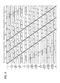
- FIG. 19 shows such a state.
- FIG. 19 shows values of solutions of the equation of the logistic map, which are obtained by carrying out operations when n is greater than or equal to 300 and less than or equal to 500 in the condition where an initial value Xo is 0.3, a parameter b varies from 0 to 4, and n is 500.
- a solution converges to one when b is smaller than around 3
- a solution converges to two when b is around 3.1 to 3.4.
- the number of positions to which a solution converges increases to 4, 8, . . . ; thus, chaotic random numbers are generated gradually.
- a solution may be 0.5 after calculations are repeated certain times, depending on a manner in which a significant figure is obtained in arithmetic processing. Since solutions obtained after that is all 0.5, unless attention is paid to a manner in which a significant figure is obtained in arithmetic processing, the range of the repeat count of utilization of solutions, and the like, chaotic random numbers are not generated in some cases.
- Chaotic random numbers generated in such a generation method may be utilized for different cases so that random number signals used for setting the sequence in the sequence determination circuit 185 are generated.
- the sequence of light emission of light sources of, for example, red (R), green (G), and blue (B) may be determined using the last two digits of a chaotic random number obtained by generation of chaotic random numbers. Note that the number of colors of light sources in this embodiment is not particularly limited.
- FIG. 14 is a schematic external view of a liquid crystal display device.
- the liquid crystal display device in FIG. 14 includes a backlight portion 101 ; a display panel 102 in which a plurality of pixels is arranged in matrix; and a polarizing plate 103 and a polarizing plate 104 between which the display panel 102 is sandwiched.
- the backlight portion 101 light sources of three colors of red, green, and blue 105 R, 105 G, and 105 B, specifically, light sources each including a combination of light-emitting diodes (LEDs) of three colors of RGB are arranged in matrix.
- a diffuser plate 106 is placed between the display panel 102 and the backlight portion 101 in order to bring evenness of light emitted from the backlight portion 101 .
- the display panel 102 and the backlight portion 101 in FIG. 14 correspond to the display panel 181 and the backlight portion 182 in FIG. 1 , respectively. Further, it is possible to form the video signal selection circuit 183 , the control circuit 184 , the sequence determination circuit 185 , and the random number generation circuit 186 which are illustrated in FIG. 1 over an external substrate 162 illustrated in FIG. 14 .
- the polarizing plate 103 and the polarizing plate 104 may be omitted depending on a liquid crystal material of the display panel 102 .
- the number of the diffuser plate 106 may be plural and the position thereof may be another position.
- Light emission and the colors of light emission of the light sources of three colors in the backlight portion 101 are switched in accordance with a video signal supplied externally.
- a field-sequential liquid crystal display device light emission of the light sources 105 R, 105 G, and 105 B is switched temporally and transmission of light of different colors in pixels is controlled, whereby a viewer can see an image of color display.
- Light emission of the light source includes switching of luminance of the light source in accordance with a video signal for display.
- the light sources in the backlight are supposed to be light-emitting diodes, they may be another type of light sources as long as the type of light sources produce lights of desired colors.
- the light-emitting diodes provided as light sources are arranged in matrix behind the plurality of pixels.
- the display panel 102 in FIG. 14 includes a pixel portion 107 , a scan line driver circuit 108 (also referred to as a gate line driver circuit), and a signal line driver circuit 109 (also referred to as a data line driver circuit). Note that the scan line driver circuit 108 and/or the signal line driver circuit 109 may be formed outside the display panel 102 .
- the pixel portion 107 in the display panel 102 includes a plurality of pixels.
- the backlight portion 101 and the display panel 102 are electrically connected to each other through an external substrate 162 provided with a display switch circuit, a display control circuit, and the like, and flexible printed circuits (FPCs) 161 serving as external input terminals.
- an external substrate 162 provided with a display switch circuit, a display control circuit, and the like, and flexible printed circuits (FPCs) 161 serving as external input terminals.
- FPCs flexible printed circuits
- FIGS. 2A and 2B to FIG. 6 illustrate specific configuration examples and specific operation of the display panel 181 and the backlight portion 182 and are used to describe driving of the liquid crystal display device having the structure in FIG. 1 .
- a configuration example of the display panel a configuration example of the scan line driver circuit, an example of operation of the scan line driver circuit, a configuration example of the signal line driver circuit, a configuration example of the backlight portion, and an example of operation of the display panel will be described to explain the display panel.
- FIG. 2A illustrates the configuration example of the display panel.
- the display panel in FIG. 2A includes a pixel portion 10 ; a scan line driver circuit 11 ; a signal line driver circuit 12 ; 3n scan lines 131 , 3n scan lines 132 , and 3n scan lines 133 (n is a natural number of 2 or more) arranged parallel or approximately parallel to each other; and m signal lines 141 , m signal lines 142 , and m signal lines 143 (m is a natural number of 2 or more) arranged parallel or approximately parallel to each other.
- the potentials of the scan lines 131 , 132 , and 133 are controlled by the scan line driver circuit 11 .
- the potentials of the signal lines 141 , 142 , and 143 are controlled by the signal line driver circuit 12 .
- the pixel portion 10 includes a plurality of pixels 15 arranged in matrix (3n rows by m columns).
- Each of the scan lines 131 , 132 , and 133 is electrically connected to m pixels 15 provided in a given row among the plurality of pixels 15 arranged in matrix (the 3n rows by the m columns).
- each of the signal lines 141 , 142 , and 143 is electrically connected to 3n pixels 15 provided in a given column among the plurality of pixels 15 arranged in matrix (the 3n rows by the m columns).
- Start signals (GSP 1 to GSP 3 ) for the scan line driver circuit, a clock signal (GCK) for the scan line driver circuit, and drive power supply potentials such as a high power supply potential (V DD ) and a low power supply potential (V SS ) are externally input to the scan line driver circuit 11 .
- Signals such as a start signal (SSP) for the signal line driver circuit, a clock signal (SCK) for the signal line driver circuit, and video signals (DATA 1 to DATA 3 ) and drive power supply potentials such as a high power supply potential and a low power supply potential are externally input to the signal line driver circuit 12 .
- FIG. 2B illustrates an example of a circuit configuration of the pixel 15 .
- the pixel 15 in FIG. 2B includes a transistor 151 , a transistor 152 , a transistor 153 , a capacitor 154 , and a liquid crystal element 155 .
- a gate of the transistor 151 is connected to the scan line 131 .
- One of a source and a drain of the transistor 151 is connected to the signal line 141 .
- a gate of the transistor 152 is connected to the scan line 132 .
- One of a source and a drain of the transistor 152 is connected to the signal line 142 .
- a gate of the transistor 153 is connected to the scan line 133 .
- One of a source and a drain of the transistor 153 is connected to the signal line 143 .
- One electrode of the capacitor 154 is connected to the other of the source and the drain of the transistor 151 , the other of the source and the drain of the transistor 152 , and the other of the source and the drain of the transistor 153 .
- the other electrode of the capacitor 154 is connected to a wiring for supplying a capacitor potential.
- One electrode (pixel electrode) of the liquid crystal element 155 is connected to the other of the source and the drain of the transistor 151 , the other of the source and the drain of the transistor 152 , the other of the source and the drain of the transistor 153 , and the one electrode of the capacitor 154 .
- the other electrode (counter electrode) of the liquid crystal element 155 is connected to a wiring for supplying a counter potential.
- a transistor is an element that includes at least three terminals, including a gate, a drain, and a source, and includes a channel formation region between a drain region and a source region.
- a current can flow through the drain region, the channel region, and the source region.
- the source and the drain of the transistor may change depending on the structure, the operating condition, and the like of the transistor, it is difficult to define which is a source or a drain. Therefore, in this document (the specification, the claims, the drawings, and the like), a region functioning as a source or a drain is not called the source or the drain in some cases.
- one of the source and the drain may be referred to as a first terminal and the other may be referred to as a second terminal.
- one of the source and the drain may be referred to as a first electrode and the other may be referred to as a second electrode.
- one of the source and the drain may be referred to as a source region and the other may be called a drain region.
- FIG. 3 illustrates the configuration example of the scan line driver circuit 11 in the display panel illustrated in FIG. 2A .
- the scan line driver circuit 11 in FIG. 3 includes three shift registers 111 to 113 each including 3n output terminals. Note that each of the output terminals of the shift register 111 is connected to one of the 3n scan lines 131 provided in the pixel portion 10 . Each of the output terminals of the shift register 112 is connected to one of the 3n scan lines 132 provided in the pixel portion 10 . Each of the output terminals of the shift register 113 is connected to one of the 3n scan lines 133 provided in the pixel portion 10 .
- the shift register 111 drives the scan lines 131
- the shift register 112 drives the scan lines 132
- the shift register 113 drives the scan lines 133
- the shift register 111 has a function of sequentially shifting selection signals from the scan line 131 in the first row (i.e., a function of sequentially selecting the scan lines 131 every half the cycle of the clock signal (GCK) for the scan line driver circuit) by using a first start pulse signal (GSP 1 ) for the scan line driver circuit, which is input externally, as a trigger.
- GSP 1 first start pulse signal
- the shift register 112 has a function of sequentially shifting selection signals from the scan line 132 in the first row, by using a second start pulse signal (GSP 2 ) for the scan line driver circuit, which is input externally, as a trigger.
- the shift register 113 has a function of sequentially shifting selection signals from the scan line 133 in the first row, by using a third start pulse signal (GSP 3 ) for the scan line driver circuit, which is input externally, as a trigger.
- FIG. 4 shows the clock signal (GCK) for the scan line driver circuit, signals (SR 111 out) output from the 3n output terminals of the shift register 111 , signals (SR 112 out) output from the 3n output terminals of the shift register 112 , and signals (SR 113 out) output from the 3n output terminals of the shift register 113 .
- GCK clock signal
- high-level potentials are sequentially shifted from the scan line 131 provided in the first row to the scan line 131 provided in the n-th row every half the cycle of the clock signal (horizontal scan period) in the shift register 111 ; high-level potentials are sequentially shifted from the scan line 132 provided in the (n+1)-th row to the scan line 132 provided in the 2n-th row every half the cycle of the clock signal (horizontal scan period) in the shift register 112 ; and high-level potentials are sequentially shifted from the scan line 133 provided in the (2n+1)-th row to the scan line 133 provided in the 3n-th row every half the cycle of the clock signal (horizontal scan period) in the shift register 113 .
- the scan line driver circuit 11 sequentially selects m pixels 15 in the first row to m pixels 15 in the n-th row through the scan lines 131 , sequentially selects m pixels 15 in the (n+1)-th row to m pixels 15 in the 2n-th row through the scan lines 132 , and sequentially selects m pixels 15 in the (2n+1)-th row to m pixels 15 in the 3n-th row through the scan lines 133 .
- the scan line driver circuit 11 can supply selection signals to 3m pixels 15 provided in different three rows every horizontal scan period.
- a sampling period (t 2 ) although output signals of the shift registers 111 to 113 are different from those in the sampling period (t 1 ), the following operation is the same as that in the sampling period (t 1 ): one of the shift registers 111 to 113 (the shift register 113 in the sampling period (t 2 )) sequentially selects the m pixels 15 provided in the first row to the m pixels 15 provided in the n-th row; another one of the shift registers 111 to 113 that is different from the one of the shift registers 111 to 113 (the shift register 111 in the sampling period (t 2 )) sequentially selects the m pixels 15 provided in the (n+1)-th row to the m pixels 15 provided in the 2n-th row; and the other of the shift registers 111 to 113 that is different from the two of the shift registers 111 to 113 (the shift register 112 in the sampling period (t 2 )) sequentially selects the m pixels 15 provided in the (2n+1)-th row to the
- FIG. 5A illustrates the configuration example of the signal line driver circuit 12 in the display panel illustrated in FIG. 2A .
- the signal line driver circuit 12 in FIG. 5A includes a shift register 120 having m output terminals, m transistors 121 , m transistors 122 , and m transistors 123 .
- a gate of the transistor 121 is connected to the j-th output terminal (j is a natural number that is 1 or more and m or less) of the shift register 120 ; one of a source and a drain of the transistor 121 is connected to a wiring for supplying the first video signal (DATA 1 ); and the other of the source and the drain of the transistor 121 is connected to the signal line 141 provided in the j-th column in the pixel portion 10 .
- a gate of the transistor 122 is connected to the j-th output terminal of the shift register 120 ; one of a source and a drain of the transistor 122 is connected to a wiring for supplying the second video signal (DATA 2 ); and the other of the source and the drain of the transistor 122 is connected to the signal line 142 provided in the j-th column in the pixel portion 10 .
- a gate of the transistor 123 is connected to the j-th output terminal of the shift register 120 ; one of a source and a drain of the transistor 123 is connected to a wiring for supplying the third video signal (DATA 3 ); and the other of the source and the drain of the transistor 123 is connected to the signal line 143 provided in the j-th column in the pixel portion 10 .
- a red (R) video signal (a video signal held in the pixel 15 when red (R) light is emitted from the backlight) is supplied to the signal line 141 ;
- a blue (B) video signal is supplied to the signal line 142 ;
- a green (G) video signal is supplied to the signal line 143 .
- FIG. 5B illustrates the configuration example of the backlight portion provided behind the pixel portion 10 in the display panel illustrated in FIG. 2A .
- the backlight in FIG. 5B includes a plurality of light sources 16 of three colors of red (R), green (G), and blue (B).
- the plurality of light sources 16 are arranged in matrix and light emission of the light sources 16 can be controlled in each given region.
- the light source 16 is provided for at least every k rows by m columns (here, k is n/4 and a natural number of 2 or more) for a backlight for the plurality of pixels 15 provided in the 3n rows by the m columns.
- Light emission of the light sources 16 can be controlled independently.
- the backlight includes at least the light source for the first to the k-th rows to the light source for the (2n+3k+1)-th to the 3n-th rows, and light emission of the light sources can be controlled independently.
- the display panel according to this embodiment is not limited to this structure. That is to say, in the display panel according to this embodiment, light sources that emit lights of given colors can be used in combination. For example, light sources of four colors of red (R), green (G), blue (B), and white (W), light sources of four colors of red (R), green (G), blue (B), and yellow (Y), or light sources of three colors of cyan (C), magenta (M), and yellow (Y) can be used in combination.
- light sources of six colors of pale red (R), pale green (G), pale blue (B), deep red (R), deep green (G), and deep blue (B), or light sources of six colors of red (R), green (G), blue (B), cyan (C), magenta (M), and yellow (Y) can be used in combination.
- light sources of the backlight the following may be used: a structure where a light source that emit white (W) light is used in addition to light sources of red (R), green (G), and blue (B), or a structure where light sources of red (R), green (G), and blue (B) emit lights at the same time to serve as a light source that emit white (W) light so that lights of four colors can be emitted from the backlight.
- any one of combinations of two of light sources of red (R) and cyan (C), green (G) and magenta (M), and blue (B) and yellow (Y) of the backlight may emit lights at the same time.
- R red
- C red
- M green
- B blue
- Y yellow
- the display panel described above has a structure where light sources of three colors of red (R), green (G), and blue (B) are arranged laterally and linearly as light sources of the backlight (see FIG. 5B ); however, the structure is not limited thereto.
- the light sources of the three colors may be arranged in triangle, or the light sources of the three colors may be arranged longitudinally and linearly.
- the display panel described above includes a direct-lit backlight as the backlight (see FIG. 5B ); however, an edge-lit backlight may be used as the backlight.
- FIG. 6 shows scanning of selection signals in the display panel and timings of light emission of the light sources in the backlight portion.
- the m pixels 15 provided in the first row to the m pixels 15 provided in the n-th row are sequentially selected; the m pixels 15 provided in the (n+1)-th row to the m pixels 15 provided in the 2n-th row are sequentially selected; and the m pixels 15 provided in the (2n+1)-th row to the m pixels 15 provided in the 3n-th row are sequentially selected, so that video signals can be input to the pixels.
- a region provided with the m pixels 15 in the first row to the m pixels 15 in the n-th row is also referred to as a first pixel region.
- a region provided with the m pixels 15 in the (n+1)-th row to the m pixels 15 provided in the 2n-th row is also referred to as a second pixel region.
- a region provided with the m pixels 15 in the (2n+1)-th row to the m pixels 15 provided in the 3n-th row is also referred to as a third pixel region.
- the red (R) video signals can be sequentially input to the pixels through the signal lines 141 when the transistors 151 included in the m pixels 15 provided in the first row to the transistors 151 included in the m pixels 15 provided in the n-th row are sequentially turned on through the scan lines 131 ;
- the blue (B) video signals can be sequentially input to the pixels through the signal lines 142 when the transistors 152 included in the m pixels 15 provided in the (n+1)-th row to the transistors 152 included in the m pixels 15 provided in the 2n-th row are sequentially turned on through the scan lines 132 ;
- the green (G) video signals can be sequentially input to the pixels through the signal lines 143 when the transistors 153 included in the m pixels 15 provided in the (2n+1)-th row to the transistors 153 included in the m pixels 15 provided in the 3n-th row are sequentially turned on through the scan lines 133 .
- red (R) light is emitted from the light source for the first to the k-th rows after the red (R) video signals are input to the m pixels 15 provided in the first row to the m pixels 15 provided in the k-th row; blue (B) light is emitted from the light source for the (n+1)-th row to the (n+k)-th rows after the blue (B) video signals are input to the m pixels 15 provided in the (n+1)-th row to the m pixels 15 provided in the (n+k)-th row; and green (G) light is emitted from the light source for the (2n+1)-th to the (2n+k)-th rows after the green (G) video signals are input to the m pixels 15 provided in the (2n+1)-th row to the m pixels 15 provided in the (2n+k)-th row.
- scanning of a selection signal and light emission of a light source of a given color can be performed concurrently in each region (the first to the n-th rows, the (n+1)-th to the 2n-th rows, or the (2n+1)-th to the 3n-th rows).
- the light source for the first to the k-th rows is also referred to as a first light source region.
- the light source for the (n+1)-th to the (n+k)-th rows is also referred to as a second light source region.
- the light source for the (2n+1)-th to the (2n+k)-th rows is also referred to as a third light source region.
- video signals can be simultaneously supplied to pixels provided in a plurality of rows, among the pixels arranged in matrix.
- the frequency of input of a video signal to each pixel can be increased without a change in response speed of a transistor or the like included in the display panel.
- the frequency of input of a video signal to each pixel can be tripled without a change in clock frequency or the like of the scan line driver circuit.
- the display panel is preferably applied to a display panel in which images are displayed by a field sequential method or a display panel driven by high frame rate driving.
- FIG. 7A shows extraction from the timing chart of FIG. 6 , in which red (R) light is emitted from the light source for the first to the k-th rows after the red (R) video signals are input to the pixels provided in the first to the k-th rows; blue (B) light is emitted from the light source for the (n+1)-th to the (n+k)-th rows after the blue (B) video signals are input to the pixels provided in the (n+1)-th to the (n+k)-th rows; and green (G) light is emitted from the light source for the (2n+1)-th to the (2n+k)-th rows after the green (G) video signals are input to the pixels provided in the (2n+1)-th to the (2n+k)-th rows.
- red (R) light is emitted from the light source for the first to the k-th rows after the red (R) video signals are input to the pixels provided in the first to the k-th rows
- blue (B) light is e
- a color image can be displayed through a period in which the red (R) video signals are input and red (R) light is emitted, the green (G) video signals are input and green (G) light is emitted, and the blue (B) video signals are input and blue (B) light is emitted.
- This period is one frame period.
- one frame period is a period in which the blue (B) video signals are input and blue (B) light is emitted, the red (R) video signals are input and red (R) light is emitted, and the green (G) video signals are input and green (G) light is emitted.
- one frame period is a period in which the green (G) video signals are input and green (G) light is emitted, the blue (B) video signals are input and blue (B) light is emitted, and the red (R) video signals are input and red (R) light is emitted.
- FIG. 7B illustration of input of the video signals in FIG. 7A is omitted and only light emission of the light sources is illustrated.
- a period indicated by an alternate long and short dashed line 700 corresponds to one frame period.
- the sequence determination circuit 185 described in FIG. 1 determines the sequence of input of the RGB video signals in one frame period in FIGS. 7A and 7B in accordance with a signal from the random number generation circuit 186 (also referred to as a random number signal) and the sequence of light emission of the backlight in the frame period in accordance with the video signals.
- the sequence of input of the video signals depending on a random number signal from the random number generation circuit 186 and the sequence of light emission of the backlight depending on the video signals in a certain period are illustrated without illustration of input of the video signals, as in FIG. 7B .
- FIG. 7B the sequence of input of the video signals depending on a random number signal from the random number generation circuit 186 and the sequence of light emission of the backlight depending on the video signals in a certain period are illustrated without illustration of input of the video signals, as in FIG. 7B .
- red (R) light, green (G) light, and blue (B) light are sequentially emitted in the pixels in the first to the k-th rows; blue (B) light, red (R) light, and green (G) light are sequentially emitted in the pixels in the (n+1)-th to the (n+k)-th rows; and green (G) light, blue (B) light, and red (R) light are sequentially emitted in the pixels in the (2n+1)-th to the (2n+k)-th rows.
- a period indicated by an alternate long and short dashed line 701 is one frame period.
- sequence of input of the video signals depending on a random number signal from the random number generation circuit 186 and the sequence of light emission of the backlight depending on the video signals in a period different from the period in FIG. 7C are illustrated without illustration of input of the video signals, as in FIG. 7B .
- green (G) light, blue (B) light, and red (R) light are sequentially emitted in the pixels in the first to the k-th rows; red (R) light, green (G) light, and blue (B) light are sequentially emitted in the pixels in the (n+1)-th to the (n+k)-th rows; and blue (B) light, red (R) light, and green (G) light are sequentially emitted in the pixels in the (2n+1)-th to the (2n+k)-th rows.
- a period indicated by an alternate long and short dashed line 702 is one frame period.
- sequence of input of the video signals depending on a random number signal from the random number generation circuit 186 and the sequence of light emission of the backlight depending on the video signals in a period different from the periods in FIGS. 7C and 7D are illustrated without illustration of input of the video signals, as in FIG. 7B .
- FIG. 7B illustrates the sequence of input of the video signals depending on a random number signal from the random number generation circuit 186 and the sequence of light emission of the backlight depending on the video signals in a period different from the periods in FIGS. 7C and 7D.
- blue (B) light, red (R) light, and green (G) light are sequentially emitted in the pixels in the first to the k-th rows; green (G) light, blue (B) light, and red (R) light are sequentially emitted in the pixels in the (n+1)-th to the (n+k)-th rows; and red (R) light, green (G) light, and blue (B) light are sequentially emitted in the pixels in the (2n+1)-th to the (2n+k)-th rows.
- a period indicated by an alternate long and short dashed line 703 is one frame period.
- sequence of input of the video signals and the sequence of light emission of the backlight depending on the video signals which are illustrated in FIGS. 7C to 7E
- sequence of light emission of the light sources in one frame period which can be determined in accordance with a random number signal from the random number generation circuit 186
- sequence of input of the video signals depending on the sequence of light emission of the light sources in the frame period are given below.
- red (R) light, blue (B) light, and green (G) light are sequentially emitted; in the pixels in the (n+1)-th to the (n+k)-th rows, green (G) light, red (R) light, and blue (B) light are sequentially emitted; and in the pixels in the (2n+1)-th to the (2n+k)-th rows, blue (B) light, green (G) light, and red (R) light are sequentially emitted.
- green (G) light, red (R) light, and blue (B) light are sequentially emitted in the pixels in the first to the k-th rows; blue (B) light, green (G) light, and red (R) light are sequentially emitted in the pixels in the (n+1)-th to the (n+k)-th rows; and red (R) light, blue (B) light, and green (G) light are sequentially emitted in the pixels in the (2n+1)-th to the (2n+k)-th rows.
- blue (B) light, green (G) light, and red (R) light are sequentially emitted in the pixels in the first to the k-th rows; red (R) light, blue (B) light, and green (G) light are sequentially emitted in the pixels in the (n+1)-th to the (n+k)-th rows; and green (G) light, red (R) light, and blue (B) light are sequentially emitted in the pixels in the (2n+1)-th to the (2n+k)-th rows.
- the sequence of light emission of the light sources in one frame period which is illustrated in FIGS. 7C to 7E
- the sequence of input of the video signals depending on the sequence of light emission of the light sources in the frame period are determined not in a particular order but at random.
- a certain period sequentially includes the frame period indicated by the alternate long and short dashed line 701 , the frame period indicated by the alternate long and short dashed line 703 , and the frame period indicated by the alternate long and short dashed line 702 .
- FIG. 8A a certain period sequentially includes the frame period indicated by the alternate long and short dashed line 701 , the frame period indicated by the alternate long and short dashed line 703 , and the frame period indicated by the alternate long and short dashed line 702 .
- another period sequentially includes the frame period indicated by the alternate long and short dashed line 702 , the frame period indicated by the alternate long and short dashed line 702 , and the frame period indicated by the alternate long and short dashed line 701 .
- still another period sequentially includes the frame period indicated by the alternate long and short dashed line 702 , the frame period indicated by the alternate long and short dashed line 701 , and the frame period indicated by the alternate long and short dashed line 702 .
- the sequence of input of the video signals depending on a random number signal from the random number generation circuit 186 and the sequence of light emission of the backlight depending on the video signals are determined at random.
- the sequence of input of the video signals and the sequence of light emission of the backlight in one frame period are determined at random.
- video signals can be simultaneously supplied to pixels in a plurality of rows.
- the frequency of input of a video signal to each pixel can be increased. Therefore, effectual frame frequency can be increased, which leads to suppression of color breakup due to a field sequential method.
- the light sources of RGB in the backlight can emit light concurrently.
- the structure according to this embodiment enables suppression of perception of color breakup caused due to loss of perception of light emission from any one of the light sources of the plurality of colors of RGB.
- the above display panel has the structure in which video signals are simultaneously supplied to 3m pixels in given three rows in the pixel portion 10 ; however, the structure of the display panel according to this embodiment of the present invention is not limited to the above structure. That is, in the display panel according to this embodiment, video signals can be simultaneously supplied to a plurality of pixels in given plural rows in the pixel portion 10 . Note that it is obvious that in the case where the number of rows is changed, the number of rows and the number of shift registers are necessary to be the same.
- the display panel has a structure where video signals are simultaneously supplied to pixels provided in given three rows arranged at regular intervals (the interval between rows supplied with video signals is n rows of pixels) in the same period; however, the structure of the display panel according to this embodiment is not limited to such a structure.
- the display panel according to this embodiment may have a structure where video signals are simultaneously supplied to pixels in given three rows provided at irregular intervals.
- the display panel may have a structure in which video signals are simultaneously supplied to m pixels in the first row, m pixels in the (a+1)-th row (a is a natural number), and m pixels in an (a+b+1)-th row (b is a natural number other than a).
- the scan line driver circuit includes a shift register; however, the shift register can be replaced with a circuit having an equivalent function.
- the shift register can be replaced with a decoder.
- This embodiment can be implemented in appropriate combination with any of the structures described in the other embodiments.
- Embodiment 1 a structure where there are periods in each of which light sources of a backlight do not emit light before and after a period that is one frame period will be described, which is different from the structure in FIG. 6 described in Embodiment 1 showing scanning of selection signals and timings of light emission of the light sources in the backlight. Note that common description between Embodiment 1 and this embodiment will be omitted in this embodiment.
- FIG. 9 is a timing chart showing scanning of selection signals and timings of light emission of light sources in a backlight in the case where there are periods in each of which the light sources of the backlight do not emit light before and after a period that is one frame period.
- the length of the period in which the light sources in the backlight do not emit light is not particularly limited as long as display quality is not degraded.
- the m pixels 15 provided in the first row to the m pixels 15 provided in the n-th row are sequentially selected; the m pixels 15 provided in the (n+1)-th row to the m pixels 15 provided in the 2n-th row are sequentially selected; and the m pixels 15 provided in the (2n+1)-th row to the m pixels 15 provided in the 3n-th row are sequentially selected, so that video signals are input to pixels.
- the m pixels 15 provided in the first row to the m pixels 15 provided in the n-th row are sequentially selected; the m pixels 15 provided in the (n+1)-th row to the m pixels 15 provided in the 2n-th row are sequentially selected; and the m pixels 15 provided in the (2n+1)-th row to the m pixels 15 provided in the 3n-th row are sequentially selected, so that video signals are input to pixels.
- one frame period includes the period in which light emission is not performed in addition to a period in which operations in the timing chart of FIG. 6 described in Embodiment 1 are performed.
- FIG. 9 shows a structure in which scanning of selection signals and light emission of the light sources in the backlight are not performed; however, it is possible to perform scanning of selection signals and to input a video signal used for not transmitting light to each pixel.
- the sequence determination circuit 185 in FIG. 1 described in Embodiment 1 determines the sequence of input of the RGB video signals in a period shown in FIGS. 10A to 10C in accordance with a signal from the random number generation circuit 186 (also referred to as a random number signal) and the sequence of light emission of the backlight in the frame period in accordance with the video signals.
- the sequence of input of the video signals depending on a random number signal from the random number generation circuit 186 and the sequence of light emission of the backlight depending on the video signals in a certain period are illustrated without illustration of input of the video signals, as in FIG. 7B .
- FIG. 7B the sequence of input of the video signals depending on a random number signal from the random number generation circuit 186 and the sequence of light emission of the backlight depending on the video signals in a certain period are illustrated without illustration of input of the video signals, as in FIG. 7B .
- sequence of input of the video signals depending on a random number signal from the random number generation circuit 186 and the sequence of light emission of the backlight depending on the video signals in a period different from the period in FIG. 10A are illustrated without illustration of input of the video signals, as in FIG. 7B .
- FIG. 7B illustrates the sequence of input of the video signals depending on a random number signal from the random number generation circuit 186 and the sequence of light emission of the backlight depending on the video signals in a period different from the period in FIG. 10A.
- sequence of input of the video signals depending on a random number signal from the random number generation circuit 186 and the sequence of light emission of the backlight depending on the video signals in a period different from the periods in FIGS. 10A and 10B are illustrated without illustration of input of the video signals, as in FIG. 7B .
- FIG. 7B illustrates the sequence of input of the video signals depending on a random number signal from the random number generation circuit 186 and the sequence of light emission of the backlight depending on the video signals in a period different from the periods in FIGS. 10A and 10B.
- sequence of input of the video signals and the sequence of light emission of the backlight depending on the video signals which are illustrated in FIGS. 10A to 10C
- sequence of light emission of the light sources in one frame period which can be determined in accordance with a random number signal from the random number generation circuit 186
- sequence of input of the video signals depending on the sequence of light emission of the light sources in the frame period are given below.
- the sequence of light emission of the light sources in one frame period which is illustrated in FIGS. 10A to 10C
- the sequence of input of the video signals depending on the sequence of light emission of the light sources in the frame period are determined not in a particular order but at random.
- a certain period sequentially includes the frame period indicated by the alternate long and short dashed line 1001 , the frame period indicated by the alternate long and short dashed line 1003 , and the frame period indicated by the alternate long and short dashed line 1002 .
- FIG. 11A a certain period sequentially includes the frame period indicated by the alternate long and short dashed line 1001 , the frame period indicated by the alternate long and short dashed line 1003 , and the frame period indicated by the alternate long and short dashed line 1002 .
- another period sequentially includes the frame period indicated by the alternate long and short dashed line 1002 , the frame period indicated by the alternate long and short dashed line 1002 , and the frame period indicated by the alternate long and short dashed line 1001 .
- still another period sequentially includes the frame period indicated by the alternate long and short dashed line 1002 , the frame period indicated by the alternate long and short dashed line 1001 , and the frame period indicated by the alternate long and short dashed line 1002 .
- the sequence of input of the video signals depending on a random number signal from the random number generation circuit 186 and the sequence of light emission of the backlight depending on the video signals are determined at random.
- the sequence of input of the video signals and the sequence of light emission of the backlight in one frame period are determined at random.
- the length of a period in which light is emitted from the backlight is shortened; thus, it is possible to further suppress color breakup.
- This embodiment can be implemented in appropriate combination with any of the structures described in the other embodiments.
- FIGS. 12A to 12D each illustrate an example of a cross-sectional structure of a transistor.
- a transistor 410 in FIG. 12A is one of bottom-gate transistors and is also referred to as an inverted staggered transistor.
- the transistor 410 includes, over a substrate 400 having an insulating surface, a gate electrode layer 401 , a gate insulating layer 402 , a semiconductor layer 403 , a source electrode layer 405 a , and a drain electrode layer 405 b .
- the insulating film 407 which covers the transistor 410 and is in contact with the semiconductor layer 403 is provided.
- a protective insulating layer 409 is formed over the insulating film 407 .
- a transistor 420 in FIG. 12B is one of bottom-gate transistors referred to as a channel-protective type (also referred to as a channel-stop type) and is also referred to as an inverted staggered transistor.
- the transistor 420 includes, over the substrate 400 having an insulating surface, the gate electrode layer 401 , the gate insulating layer 402 , the semiconductor layer 403 , an insulating film 427 which functions as a channel protective layer covering a channel formation region of the semiconductor layer 403 , the source electrode layer 405 a , and the drain electrode layer 405 b . Further, the protective insulating layer 409 is formed so as to cover the transistor 420 .
- a transistor 430 in FIG. 12C is a bottom-gate transistor and includes, over the substrate 400 having an insulating surface, the gate electrode layer 401 , the gate insulating layer 402 , the source electrode layer 405 a , the drain electrode layer 405 b , and the semiconductor layer 403 .
- the insulating film 407 which covers the transistor 430 and is in contact with the semiconductor layer 403 is provided.
- the protective insulating layer 409 is formed over the insulating film 407 .
- the gate insulating layer 402 is provided over and in contact with the substrate 400 and the gate electrode layer 401 ; the source electrode layer 405 a and the drain electrode layer 405 b are provided over and in contact with the gate insulating layer 402 . Further, the semiconductor layer 403 is provided over the gate insulating layer 402 , the source electrode layer 405 a , and the drain electrode layer 405 b.
- a transistor 440 in FIG. 12D is one of top-gate transistors.
- the transistor 440 includes, over the substrate 400 having an insulating surface, an insulating layer 437 , the semiconductor layer 403 , the source electrode layer 405 a , the drain electrode layer 405 b , the gate insulating layer 402 , and the gate electrode layer 401 .
- a wiring layer 436 a and a wiring layer 436 b are formed in contact with and are connected to the source electrode layer 405 a and the drain electrode layer 405 b , respectively.
- amorphous silicon, microcrystalline silicon, polysilicon, an oxide semiconductor, an organic semiconductor, or the like can be used as a semiconductor material of the semiconductor layer 403 .
- a substrate that can be used as the substrate 400 having an insulating surface there is no particular limitation on a substrate that can be used as the substrate 400 having an insulating surface; a glass substrate made of barium borosilicate glass, aluminoborosilicate glass, or the like is used.
- an insulating film serving as a base film may be provided between the substrate and the gate electrode layer.
- the base film has a function of preventing diffusion of an impurity element from the substrate, and can be formed to have a single-layer structure or a layered structure using one or more of a silicon nitride film, a silicon oxide film, a silicon nitride oxide film, and a silicon oxynitride film.
- the gate electrode layer 401 may be formed to have a single-layer structure or a layered structure using any of metal materials such as molybdenum, titanium, chromium, tantalum, tungsten, aluminum, copper, neodymium, and scandium, and an alloy material containing any of these materials as its main component.
- metal materials such as molybdenum, titanium, chromium, tantalum, tungsten, aluminum, copper, neodymium, and scandium, and an alloy material containing any of these materials as its main component.
- the gate insulating layer 402 can be formed to have a single-layer or layered structure using any of a silicon oxide layer, a silicon nitride layer, a silicon oxynitride layer, a silicon nitride oxide layer, an aluminum oxide layer, an aluminum nitride layer, an aluminum oxynitride layer, an aluminum nitride oxide layer, and a hafnium oxide layer by a plasma CVD method, a sputtering method, or the like.
- a silicon nitride layer (SiN y (y>0)) with a thickness of 50 nm or more and 200 nm or less is formed as a first gate insulating layer, and a silicon oxide layer (SiO x (x>0)) with a thickness of 5 nm or more and 300 nm or less is formed as a second gate insulating layer over the first gate insulating layer, so that a gate insulating layer with a total thickness of 200 nm is formed.
- a metal film containing an element selected from Al, Cr, Cu, Ta, Ti, Mo, and W for example, a metal film containing an element selected from Al, Cr, Cu, Ta, Ti, Mo, and W, or a metal nitride film containing any of the above elements as its component (a titanium nitride film, a molybdenum nitride film, a tungsten nitride film, or the like) can be used.
- a structure may be employed in which a high-melting-point metal film of Ti, Mo, W, or the like or a metal nitride film of any of these elements (a titanium nitride film, a molybdenum nitride film, or a tungsten nitride film) may be provided over and/or below a metal layer of Al, Cu, or the like.
- a high-melting-point metal film of Ti, Mo, W, or the like or a metal nitride film of any of these elements a titanium nitride film, a molybdenum nitride film, or a tungsten nitride film
- a material similar to that of the source electrode layer 405 a and the drain electrode layer 405 b can be used for a conductive film such as the wiring layer 436 a and the wiring layer 436 b which are connected to the source electrode layer 405 a and the drain electrode layer 405 b , respectively.
- the conductive film to be the source electrode layer 405 a and drain electrode layer 405 b may be formed using a conductive metal oxide.
- a conductive metal oxide indium oxide (In 2 O 3 ), tin oxide (SnO 2 ), zinc oxide (ZnO), an indium oxide-tin oxide alloy (In 2 O 3 —SnO 2 , abbreviated to ITO), an indium oxide-zinc oxide alloy (In 2 O 3 —ZnO), or any of these metal oxide materials containing silicon oxide can be used.
- an inorganic insulating film such as a silicon oxide film, a silicon oxynitride film, an aluminum oxide film, or an aluminum oxynitride film can be typically used.
- an inorganic insulating film such as a silicon nitride film, an aluminum nitride film, a silicon nitride oxide film, or an aluminum nitride oxide film can be used.
- a planarization insulating film may be formed over the protective insulating layer 409 in order to reduce surface unevenness due to the transistor.
- an organic material such as a polyimide resin, an acrylic resin, or a benzocyclobutene resin can be used.
- a low-dielectric constant material a low-k material or the like.
- the planarization insulating film may be formed by stacking a plurality of insulating films formed using any of these materials.
- This embodiment can be implemented in appropriate combination with any of the structures described in the other embodiments.
- FIG. 15A is an example of a plan view of a pixel.
- FIG. 15B is a cross-sectional view along alternate long and short dashed line A-B in FIG. 15A .
- a signal line formed of the same wiring layer as a drain electrode layer 1901 b and including a source electrode layer 1901 a is provided to extend in a longitudinal direction (column direction).
- Wiring layers (including a gate electrode layer 1903 ) serving as scan lines extend in the direction approximately orthogonal to the source electrode layer 1901 a (in the horizontal direction (row direction) in the diagram).
- a capacitor wiring layer 1904 extends in the direction approximately parallel to the gate electrode layer 1903 and in the direction approximately orthogonal to the source electrode layer 1901 a (in the horizontal direction (row direction) in the diagram).
- a transistor 1905 including the gate electrode layer 1903 is provided.
- a stack of the capacitor wiring layer 1904 , the gate insulating layer 1912 , and the drain electrode layer 1901 b forms a capacitor 1915 .
- An insulating film 1907 and an interlayer film 1909 are provided over the transistor 1905 .
- An opening (contact hole) is formed in the insulating film 1907 and the interlayer film 1909 which are over the transistor 1905 .
- the pixel illustrated in FIGS. 15A and 15B includes a transparent electrode layer 1910 as an electrode layer connected to the transistor 1905 on the first substrate 1918 side, and a transparent electrode layer 1920 on the second substrate 1919 side.
- the transparent electrode layer 1910 and the transistor 1905 are connected to each other in the opening (contact hole).
- the transparent electrode layer 1910 and the transparent electrode layer 1920 overlap with each other with a liquid crystal layer 1917 provided therebetween.
- a light blocking layer 1911 black matrix
- the transistor 1905 in FIGS. 15A and 15B includes a semiconductor layer 1913 formed over the gate electrode layer 1903 with the gate insulating layer 1912 provided therebetween; and the source electrode layer 1901 a and the drain electrode layer 1901 b which are in contact with the semiconductor layer 1913 .
- An insulating material containing oxygen and a Group 13 element is preferably used for an insulating layer (the gate insulating layer 1912 and the insulating film 1907 in this embodiment) in contact with the semiconductor layer 1913 including an oxide semiconductor (the semiconductor layer is also referred to as an oxide semiconductor).
- oxide semiconductor materials include Group 13 elements, and an insulating material containing a Group 13 element is compatible with an oxide semiconductor. Thus, when an insulating material containing a Group 13 element is used for an insulating layer in contact with an oxide semiconductor, the state of the interface with the oxide semiconductor can be kept well.
- An insulating material containing a Group 13 element refers to an insulating material containing one or more Group 13 elements.
- a gallium oxide, an aluminum oxide, an aluminum gallium oxide, a gallium aluminum oxide, and the like are given.
- an aluminum gallium oxide contains gallium and aluminum so that the aluminum content is higher than the gallium content in atomic percent
- a gallium aluminum oxide contains gallium and aluminum so that the gallium content is higher than the aluminum content in atomic percent.
- An insulating material of the insulating layer in contact with the semiconductor layer 1913 including an oxide semiconductor preferably contains oxygen in a proportion higher than that in the stoichiometric composition, by heat treatment in an oxygen atmosphere or oxygen doping.
- Oxygen doping refers to addition of oxygen into a bulk. Note that the term “bulk” is used in order to clarify that oxygen is added not only to a surface of a thin film but also to the inside of the thin film.
- oxygen doping includes “oxygen plasma doping” in which oxygen in the form of plasma is added to a bulk. The oxygen doping may be performed by an ion implantation method or an ion doping method.
- the composition of the gallium aluminum oxide (aluminum gallium oxide) can be set to be Ga x Al 2-x O 3+ ⁇ (0 ⁇ x ⁇ 2, 0 ⁇ 1) by heat treatment in an oxygen atmosphere or oxygen doping.
- an insulating layer including a region where the proportion of oxygen is higher than that in the stoichiometric composition can be formed.
- the oxide semiconductor layer can be an i-type or substantially i-type oxide semiconductor.
- the insulating layer including a region where the proportion of oxygen is higher than that in the stoichiometric composition may be applied to either the insulating layer positioned over the semiconductor layer 1913 including an oxide semiconductor or the insulating layer positioned below the semiconductor layer 1913 including an oxide semiconductor of the insulating layers in contact with the semiconductor layer 1913 including an oxide semiconductor; however, it is preferable to apply such an insulating layer to both of the insulating layers.
- the aforementioned effect can be enhanced with a structure where the insulating layers each including a region where the proportion of oxygen is higher than that in the stoichiometric composition are used as the insulating layers which are in contact with and over and below the semiconductor layer 1913 including an oxide semiconductor, in order that the semiconductor layer 1913 including an oxide semiconductor is sandwiched between the insulating layers.
- the insulating layers over and below the semiconductor layer 1913 including an oxide semiconductor may include the same constituent element or different constituent elements.
- the insulating layer in contact with the semiconductor layer 1913 including an oxide semiconductor may be formed by stacking insulating layers each including a region where the proportion of oxygen is higher than that in the stoichiometric composition.
- the insulating layer below the semiconductor layer 1913 including an oxide semiconductor may be formed by stacking insulating layers each including a region where the proportion of oxygen is higher than that in the stoichiometric composition. Further, both of the insulating layers over and below the semiconductor layer 1913 including an oxide semiconductor may be formed by stacking insulating layers each including a region where the proportion of oxygen is higher than that in the stoichiometric composition.
- the gate electrode layer 1903 is provided so as to overlap with the lower side of the semiconductor layer 1913 and the light-blocking layer 1911 is provided so as to cover the upper side of the semiconductor layer 1913 .
- the transistor 1905 can be shielded from light from the upper side and the lower side. Blocking of light results in suppression of degradation of transistor characteristics.
- FIG. 16A is an example of a plan view illustrating a pixel different from that in FIG. 15A .
- FIG. 16B is a cross-sectional view along alternate long and short dashed line C-D in FIG. 16A . Note that reference numerals of components in FIGS. 16A and 16B are the same as those in FIGS. 15A and 15B and thus description thereof will be omitted.
- a structure in the plan view and the cross-sectional view of FIGS. 16A and 16B is different from that of FIGS. 15A and 15B in that the source electrode layer 1901 a and the drain electrode layer 1901 b are provided so as to cover regions of the semiconductor layer 1913 except a channel formation region. Accordingly, the transistor 1905 can be shielded from light also at end portions of the semiconductor layer 1913 . Blocking of light results in suppression of degradation of transistor characteristics.
- FIG. 17A is an example of a plan view illustrating a pixel different from those in FIG. 15A and FIG. 16A .
- FIG. 17B is a cross-sectional view along alternate long and short dashed line E-F in FIG. 17A . Note that reference numerals of components in FIGS. 17A and 17B are the same as those in FIGS. 15A and 15B and thus description thereof will be omitted.
- a structure in the plan view and the cross-sectional view of FIGS. 17A and 17B is similar to that of FIGS. 15A and 15B in that the gate electrode layer 1903 is provided so as to overlap with the lower side of the semiconductor layer 1913 and the light-blocking layer 1911 is provided so as to cover the upper side of the semiconductor layer 1913 .
- the structure in the plan view and the cross-sectional view of FIGS. 17A and 17B is similar to that of FIGS. 16A and 16B in that the source electrode layer 1901 a and the drain electrode layer 1901 b are provided so as to cover regions of the semiconductor layer 1913 except a channel formation region. Accordingly, the transistor 1905 can be shielded from light from the upper side and the lower side and at end portions of the semiconductor layer 1913 . Blocking of light results in suppression of degradation of transistor characteristics.
- This embodiment can be implemented in appropriate combination with any of the structures described in the other embodiments.
- a layer 6116 to be separated is formed over a formation substrate 6200 with a separation layer 6201 provided therebetween (see FIG. 20A ).
- the formation substrate 6200 may be a quartz substrate, a sapphire substrate, a ceramic substrate, a glass substrate, a metal substrate, or the like. Note that such a substrate which is not thin enough to be definitely flexible enables precise formation of an element such as a transistor. “Not definitely flexible” means that the elastic modulus of the substrate is higher than or equivalent to that of a glass substrate used in generally fabricating a liquid crystal display.
- the separation layer 6201 is formed to have a single-layer or layered structure using any of elements selected from tungsten (W), molybdenum (Mo), titanium (Ti), tantalum (Ta), niobium (Nb), nickel (Ni), cobalt (Co), zirconium (Zr), zinc (Zn), ruthenium (Ru), rhodium (Rh), palladium (Pd), osmium (Os), iridium (Ir), and silicon (Si), an alloy material containing any of the above elements as its main component, and a compound material containing any of the above elements as its main component by a sputtering method, a plasma CVD method, an application method, a printing method, or the like.
- a tungsten layer, a molybdenum layer, or a layer containing a mixture of tungsten and molybdenum is preferably formed.
- a layer containing an oxide or an oxynitride of tungsten, a layer containing an oxide or an oxynitride of molybdenum, or a layer containing an oxide or an oxynitride of a mixture of tungsten and molybdenum is formed.
- the mixture of tungsten and molybdenum corresponds to an alloy of tungsten and molybdenum, for example.
- a metal layer and a metal oxide layer be formed as a first layer and a second layer, respectively.
- a metal layer and a metal oxide layer be formed as a first layer and a second layer, respectively.
- an oxide layer such as a silicon oxide which can be utilized as an insulating layer
- an oxide layer such as a silicon oxide which can be utilized as an insulating layer
- the layer 6116 to be separated is provided with components necessary for an element substrate, such as a transistor, an interlayer insulating film, a wiring, and a pixel electrode, and depending on a case, a common electrode, a color filter, a black matrix, or an alignment film.
- Such components can be normally formed over the separation layer 6201 .
- the transistor and the electrode can be formed precisely using a known material and a known method.
- the layer 6116 to be separated is bonded to a temporary supporting substrate 6202 with the use of an adhesive 6203 for separation and then, the layer 6116 to be separated is separated from the separation layer 6201 over the formation substrate 6200 to be transferred (see FIG. 20B ).
- the layer 6116 to be separated is placed on the temporary supporting substrate side.
- a process for transferring the layer to be separated from the formation substrate to the temporary supporting substrate is referred to as a transfer process.
- a glass substrate, a quartz substrate, a sapphire substrate, a ceramic substrate, a metal substrate, or the like can be used as the temporary supporting substrate 6202 .
- a plastic substrate which can withstand the temperature of the following process may be used.
- an adhesive which is soluble in water or a solvent, an adhesive which is capable of being plasticized upon irradiation of UV light, or the like is used so that the temporary supporting substrate 6202 and the layer 6116 to be separated can be chemically or physically separated when necessary.
- any of various methods can be used as appropriate in the process for transferring the layer 6116 to be separated to the temporary supporting substrate 6202 .
- a film including a metal oxide film is formed as the separation layer 6201 so as to be in contact with the layer 6116 to be separated, the metal oxide film is embrittled by crystallization, whereby the layer 6116 to be separated can be separated from the formation substrate.
- an amorphous silicon film containing hydrogen is formed as the separation layer 6201 between the formation substrate 6200 and the layer 6116 to be separated, the amorphous silicon film containing hydrogen is removed by laser light irradiation or etching, so that the layer 6116 to be separated can be separated from the formation substrate 6200 .
- the separation layer 6201 When a film containing nitrogen, oxygen, hydrogen, or the like (for example, an amorphous silicon film containing hydrogen, an alloy film containing hydrogen, an alloy film containing oxygen, or the like) is used as the separation layer 6201 , the separation layer 6201 is irradiated with laser light to release the nitrogen, oxygen, or hydrogen contained in the separation layer 6201 as a gas, so that separation between the layer 6116 to be separated and the formation substrate 6200 can be promoted. Alternatively, liquid may be made to penetrate the interface between the separation layer 6201 and the layer 6116 to be separated to cause separation of the layer 6116 to be separated from the formation substrate 6200 . Still alternatively, when the separation layer 6201 is formed using tungsten, the separation may be performed while the separation layer 6201 is etched with the use of a mixed solution of ammonia water and a hydrogen peroxide solution.
- a film containing nitrogen, oxygen, hydrogen, or the like for example, an amorphous silicon film containing hydrogen, an alloy film containing hydrogen, an
- the separation process can be facilitated by using plural kinds of separation methods described above in combination. That is, the separation can be performed with physical force (by a machine or the like) after performing laser light irradiation on part of the separation layer, etching on part of the separation layer with a gas, a solution, or the like, or mechanical removal of part of the separation layer with a sharp knife, a scalpel, or the like, in order that the separation layer and the layer to be separated can be easily separated from each other.
- the layer to be separated can be physically separated easily from the separation layer by using, for example, a groove formed by laser light irradiation or a scratch made by a sharp knife, a scalpel, or the like as a trigger.
- the separation may be performed while liquid such as water is poured.
- a method for separating the layer 6116 to be separated from the formation substrate 6200 may alternatively be employed in which the formation substrate 6200 over which the layer 6116 to be separated is formed is removed by mechanical polishing or by etching using a solution or a halogen fluoride gas such as NF 3 , BrF 3 , or ClF 3 , or the like. In that case, the separation layer 6201 is not necessarily provided.
- a surface of the layer 6116 to be separated or the separation layer 6201 which is exposed due to separation of the layer 6116 to be separated from the formation substrate 6200 , is bonded to a transfer substrate 6110 with the use of a first adhesive layer 6111 including an adhesive different from the adhesive 6203 for separation (see FIG. 20 C 1 ).
- various curable adhesives e.g., a light curable adhesive such as a UV curable adhesive, a reactive curable adhesive, a thermal curable adhesive, and an anaerobic adhesive can be used.
- a light curable adhesive such as a UV curable adhesive, a reactive curable adhesive, a thermal curable adhesive, and an anaerobic adhesive.
- various substrates with high toughness such as an organic resin film and a metal substrate, can be preferably used.
- Substrates with high toughness have high impact resistance and thus are less likely to be damaged.
- An organic resin film and a thin metal substrate, which are lightweight, enable significant weight reduction as compared to a general glass substrate. When such a substrate is used, it is possible to fabricate a lightweight display device which is not easily damaged.
- a substrate which has high toughness and transmits visible light may be used as the transfer substrate 6110 .
- polyester resins such as polyethylene terephthalate (PET) and polyethylene naphthalate (PEN)
- an acrylic resin such as a polymethyl methacrylate resin, a polyacrylonitrile resin, a polyimide resin, a polycarbonate (PC) resin, a polyethersulfone (PES) resin, a polyamide resin, a cycloolefin resin, a polystyrene resin, a polyamide imide resin, and a polyvinylchloride resin
- PET polyethylene terephthalate
- PEN polyethylene naphthalate
- acrylic resin such as a polymethyl methacrylate resin, a polyacrylonitrile resin, a polyimide resin, a polycarbonate (PC) resin, a polyethersulfone (PES) resin, a polyamide resin, a cycloolefin resin, a polys
- a substrate made of such an organic resin has high toughness and thus has high impact resistance and is less likely to be damaged. Further, a film of such an organic resin, which is lightweight, enables significant reduction in weight of a display device as compared to a general glass substrate.
- the transfer substrate 6110 is preferably further provided with a metal plate 6206 having an opening at least in a portion overlapping with a region where light of each pixel is transmitted.
- the transfer substrate 6110 which has high toughness and high impact resistance and is less likely to be damaged can be formed while a change in dimension is suppressed.
- the transfer substrate 6110 which is lighter than a general glass substrate can be formed. When such a substrate is used, it is possible to fabricate a lightweight display device which is not easily damaged (see FIG. 20 D 1 ).
- FIG. 21A is an example of a top view of a liquid crystal display device.
- the metal plate 6206 having openings formed in a grid so as to leave a portion overlapping with the first wiring layer 6210 and/or the second wiring layer 6211 as in FIG. 21B may be used. Attachment of the metal plate 6206 makes it possible to suppress a change in dimension due to unfavorable alignment or extension of a substrate because of the use of a substrate made of an organic resin.
- the polarizing plate may be provided between the transfer substrate 6110 and the metal plate 6206 or outside the metal plate 6206 .
- the polarizing plate may be attached to the metal plate 6206 in advance. Note that in terms of weight reduction, a substrate which is thin but has dimension stability is preferably used as the metal plate 6206 .
- the temporary supporting substrate 6202 is separated from the layer 6116 to be separated. Since the adhesive 6203 for separation includes a material capable of separating the temporary supporting substrate 6202 and the layer 6116 to be separated from each other when necessary, the temporary supporting substrate 6202 may be separated by a method depending on the material. Note that light is emitted from the backlight as shown by arrows in the drawing (see FIG. 20 E 1 ).
- the layer 6116 to be separated which is provided with components such as the transistor and the pixel electrode (a common electrode, a color filter, a black matrix, an alignment film, or the like may be provided as necessary), can be formed over the transfer substrate 6110 , whereby a lightweight element substrate with high impact resistance can be formed.
- the display device having the above structure is one embodiment of the present invention, and the present invention also includes a display device having a structure different from that of the above display device.
- the metal plate 6206 may be attached to a surface of the exposed separation layer 6201 or the layer 6116 to be separated before attachment of the transfer substrate 6110 (see FIG. 20 C 2 ).
- a barrier layer 6207 is preferably provided between the metal plate 6206 and the layer 6116 to be separated so that a contaminant from the metal plate 6206 can be prevented from adversely affecting characteristics of the transistor in the layer 6116 to be separated.
- the barrier layer 6207 may be provided over the surface of the exposed separation layer 6201 or the layer 6116 to be separated before attachment of the metal plate 6206 .
- a barrier film may be formed using an inorganic material, an organic material, or the like; typically, a silicon nitride and the like can be used.
- a material of the barrier film is not limited to the above as long as contamination of the transistor can be prevented.
- the barrier film is formed using a light-transmitting material or formed to a thickness small enough to transmit light so that the barrier film can transmit at least visible light.
- the metal plate 6206 may be bonded with the use of a second adhesive layer (not illustrated) including an adhesive different from the adhesive 6203 for separation.
- the first adhesive layer 6111 is formed over a surface of the metal plate 6206 and the transfer substrate 6110 is attached to the first adhesive layer 6111 (FIG. 20 D 2 ) and the temporary supporting substrate 6202 is separated from the layer 6116 to be separated (FIG. 20 E 2 ), whereby a lightweight element substrate with high impact resistance can be formed similarly. Note that light is emitted from the backlight as shown by arrows in the drawing.
- the lightweight element substrate with high impact resistance formed as described above is firmly attached to a counter substrate with the use of a sealant with a liquid crystal layer provided between the substrates, whereby a lightweight liquid crystal display device with high impact resistance can be manufactured.
- a counter substrate a substrate which has high toughness and transmits visible light (similar to a plastic substrate which can be used as the transfer substrate 6110 ) can be used.
- a polarizing plate, a color filter, a black matrix, a common electrode, or an alignment film may be provided as necessary.
- a dispenser method, an injection method, or the like can be employed as in the conventional case.
- the lightweight liquid crystal display device with high impact resistance manufactured as described above a fine element such as the transistor can be formed over a glass substrate or the like which has relatively high dimensional stability, and the conventional manufacturing method can be applied, so that even such a fine element can be formed precisely. Therefore, the lightweight liquid crystal display device with high impact resistance can display images with high precision and high quality.
- liquid crystal display device manufactured as described above may be flexible.
- This embodiment can be implemented in appropriate combination with any of the structures described in the other embodiments.
- a liquid crystal display device disclosed in this specification can be applied to a variety of electronic appliances (including game machines).
- electronic appliances are a television set (also referred to as a television or a television receiver), a monitor of a computer or the like, a camera such as a digital camera or a digital video camera, a digital photo frame, a mobile phone handset (also referred to as a mobile phone or a mobile phone device), a portable game machine, a portable information terminal, an audio reproducing device, a large-sized game machine such as a pachinko machine, and the like.
- Examples of electronic appliances each including the liquid crystal display device described in the above embodiment are described.
- FIG. 13A illustrates an example of an electronic book reader.
- the electronic book reader in FIG. 13A includes two housings, a housing 1700 and a housing 1701 .
- the housing 1700 and the housing 1701 are combined with a hinge 1704 so that the electronic book reader can be opened and closed. With such a structure, the electronic book reader can operate like a paper book.
- a display portion 1702 and a display portion 1703 are incorporated in the housing 1700 and the housing 1701 , respectively.
- the display portion 1702 and the display portion 1703 may display one image or different images.
- the display portion 1702 and the display portion 1703 display different images, for example, text can be displayed on a display portion on the right side (the display portion 1702 in FIG. 13A ) and graphics can be displayed on a display portion on the left side (the display portion 1703 in FIG. 13A ).
- FIG. 13A illustrates an example in which the housing 1700 is provided with an operation portion and the like.
- the housing 1700 is provided with a power input terminal 1705 , operation keys 1706 , a speaker 1707 , and the like.
- the operation key 1706 pages can be turned.
- a keyboard, a pointing device, or the like may also be provided on the surface of the housing, on which the display portion is provided.
- an external connection terminal e.g., an earphone terminal, a USB terminal, or a terminal connectable to a variety of cables such as a USB cable
- a recording medium insertion portion, and the like may be provided on the back surface or the side surface of the housing.
- the electronic book reader in FIG. 13A may have a function of an electronic dictionary.
- FIG. 13B illustrates an example of a digital photo frame.
- a display portion 1712 is incorporated in a housing 1711 .
- the display portion 1712 can display a variety of images.
- the display portion 1712 can display data of an image taken with a digital camera or the like and function as a normal photo frame.
- the digital photo frame in FIG. 13B is provided with an operation portion, an external connection terminal (a USB terminal, a terminal connectable to a variety of cables such as a USB cable, or the like), a recording medium insertion portion, and the like.
- an external connection terminal a USB terminal, a terminal connectable to a variety of cables such as a USB cable, or the like
- a recording medium insertion portion and the like.
- these components may be provided on the same surface as the display portion, it is preferable to provide them on the side surface or the back surface for design aesthetics.
- a memory storing data of an image taken with a digital camera is inserted in the recording medium insertion portion of the digital photo frame and the data is loaded, whereby the image can be displayed on the display portion 1712 .
- FIG. 13C illustrates an example of a television set including a liquid crystal display device.
- a display portion 1722 is incorporated in a housing 1721 .
- the display portion 1722 can display an image.
- the housing 1721 is supported by a stand 1723 .
- the liquid crystal display device described in any of the above embodiments can be used for the display portion 1722 .
- the television set in FIG. 13C can be operated with an operation switch of the housing 1721 or a separate remote controller. Channels and volume can be controlled with an operation key of the remote controller so that an image displayed on the display portion 1722 can be controlled. Further, the remote controller may be provided with a display portion for displaying data output from the remote controller.
- FIG. 13D illustrates an example of a mobile phone including a liquid crystal display device.
- the mobile phone illustrated in FIG. 13D is provided with a display portion 1732 incorporated in a housing 1731 , an operation button 1733 , an operation button 1737 , an external connection port 1734 , a speaker 1735 , a microphone 1736 , and the like.
- the display portion 1732 of the mobile phone in FIG. 13D is a touchscreen.
- contents displayed on the display portion 1732 can be controlled. Further, operations such as making calls and composing mails can be performed by touching the display portion 1732 with a finger or the like.
- This embodiment can be implemented in appropriate combination with any of the structures described in the other embodiments.
Abstract
Description
- [Patent Document 1] Japanese Published Patent Application No. 2009-042405
x n+1 =r(x n) n=0,1, . . . [EQUATION 1]
r(x n)=bx n(1−x n) [EQUATION 3]
r(x n)=cos(n cos−1 x n) [EQUATION 5]
Claims (32)
Applications Claiming Priority (4)
| Application Number | Priority Date | Filing Date | Title |
|---|---|---|---|
| JP2010144883 | 2010-06-25 | ||
| JP2010-145143 | 2010-06-25 | ||
| JP2010145143 | 2010-06-25 | ||
| JP2010-144883 | 2010-06-25 |
Publications (2)
| Publication Number | Publication Date |
|---|---|
| US20110316818A1 US20110316818A1 (en) | 2011-12-29 |
| US9047840B2 true US9047840B2 (en) | 2015-06-02 |
Family
ID=45352073
Family Applications (1)
| Application Number | Title | Priority Date | Filing Date |
|---|---|---|---|
| US13/159,593 Expired - Fee Related US9047840B2 (en) | 2010-06-25 | 2011-06-14 | Display device and electronic appliance |
Country Status (5)
| Country | Link |
|---|---|
| US (1) | US9047840B2 (en) |
| JP (2) | JP2012027458A (en) |
| KR (1) | KR20130116857A (en) |
| TW (1) | TWI527014B (en) |
| WO (1) | WO2011162166A1 (en) |
Families Citing this family (7)
| Publication number | Priority date | Publication date | Assignee | Title |
|---|---|---|---|---|
| WO2012002197A1 (en) | 2010-07-02 | 2012-01-05 | Semiconductor Energy Laboratory Co., Ltd. | Liquid crystal display device |
| CN106057144B (en) | 2010-07-02 | 2019-03-12 | 株式会社半导体能源研究所 | Liquid crystal display device and the method for driving liquid crystal display device |
| KR101956216B1 (en) | 2010-08-05 | 2019-03-08 | 가부시키가이샤 한도오따이 에네루기 켄큐쇼 | Driving method of liquid crystal display device |
| JP2012103683A (en) | 2010-10-14 | 2012-05-31 | Semiconductor Energy Lab Co Ltd | Display device and driving method for the same |
| JP2014032399A (en) | 2012-07-13 | 2014-02-20 | Semiconductor Energy Lab Co Ltd | Liquid crystal display device |
| CN105445987A (en) * | 2016-01-07 | 2016-03-30 | 浙江宇视科技有限公司 | Automatic protection method and device of liquid crystal spliced screen |
| JP7317795B2 (en) | 2018-02-23 | 2023-07-31 | 株式会社半導体エネルギー研究所 | Display device |
Citations (31)
| Publication number | Priority date | Publication date | Assignee | Title |
|---|---|---|---|---|
| JPH0659885A (en) | 1992-08-10 | 1994-03-04 | Matsushita Electric Ind Co Ltd | Bit search circuit |
| US5421576A (en) | 1992-10-31 | 1995-06-06 | Semiconductor Energy Laboratory Co., Ltd. | Game machine |
| US5735741A (en) | 1995-05-17 | 1998-04-07 | Semiconductor Energy Laboratory Co., Ltd. | Game machine with chaotic number generator |
| JPH11258573A (en) | 1998-03-16 | 1999-09-24 | Nec Corp | Method and device for driving liquid crystal display element |
| JPH11337904A (en) | 1998-05-11 | 1999-12-10 | Internatl Business Mach Corp <Ibm> | Liquid crystal display device |
| JP2001133746A (en) | 1999-11-08 | 2001-05-18 | Fujitsu Ltd | Liquid crystal display device |
| US6597348B1 (en) | 1998-12-28 | 2003-07-22 | Semiconductor Energy Laboratory Co., Ltd. | Information-processing device |
| US20040059517A1 (en) * | 2002-07-01 | 2004-03-25 | Szajnowski Wieslaw Jerzy | Signal statistics determination |
| JP2005295347A (en) | 2004-04-02 | 2005-10-20 | Hitachi Ltd | Image display |
| US20060038761A1 (en) * | 2004-02-17 | 2006-02-23 | Yuh-Ren Shen | Method and device for driving liquid crystal display |
| WO2006067750A2 (en) | 2004-12-22 | 2006-06-29 | Tpo Hong Kong Holding Limited | Backlight system display method and apparatus, and backlight system |
| JP2006220685A (en) | 2005-02-08 | 2006-08-24 | 21 Aomori Sangyo Sogo Shien Center | Method and device for driving divisional drive field sequential color liquid crystal display using scan backlight |
| US7161573B1 (en) | 1998-02-24 | 2007-01-09 | Nec Corporation | Liquid crystal display unit and method for driving the same |
| WO2007049489A1 (en) | 2005-10-24 | 2007-05-03 | Rohm Co., Ltd. | Backlight device and image display device using the same |
| JP2007264211A (en) | 2006-03-28 | 2007-10-11 | 21 Aomori Sangyo Sogo Shien Center | Color display method for color-sequential display liquid crystal display apparatus |
| US20070279374A1 (en) | 2006-06-02 | 2007-12-06 | Semiconductor Energy Laboratory Co., Ltd. | Liquid crystal display device, driving method of the same, and electronic device using the same |
| US7317438B2 (en) | 1998-10-30 | 2008-01-08 | Semiconductor Energy Laboratory Co., Ltd. | Field sequential liquid crystal display device and driving method thereof, and head mounted display |
| US7385579B2 (en) | 2000-09-29 | 2008-06-10 | Semiconductor Energy Laboratory Co., Ltd. | Liquid crystal display device and method of driving the same |
| US7403177B2 (en) | 2002-11-29 | 2008-07-22 | Semiconductor Energy Laboratory Co., Ltd. | Display device, driving method thereof, and electronic apparatus |
| US20080273006A1 (en) * | 2007-05-03 | 2008-11-06 | Novatek Microelectronics Corp. | Color-zone layout of light-emitting module and controlling method of color sequence |
| JP2009042405A (en) | 2007-08-08 | 2009-02-26 | Epson Imaging Devices Corp | Liquid crystal display device |
| US20090231324A1 (en) * | 2008-03-11 | 2009-09-17 | Hitachi Displays, Ltd. | Liquid crystal display device |
| US20100039450A1 (en) * | 2008-08-13 | 2010-02-18 | Chih-Yu Lin | Circuit for Controlling Color Sequential Liquid Crystal Display and Method for Controlling the Same |
| US7702705B2 (en) | 2005-03-15 | 2010-04-20 | Kabushiki Kaisha Toshiba | Random number generation circuit |
| US7724340B2 (en) * | 2007-01-18 | 2010-05-25 | Samsung Electronics Co., Ltd. | Liquid crystal display panel having power supply lines and liquid crystal display |
| US7773066B2 (en) | 1999-03-26 | 2010-08-10 | Semiconductor Energy Laboratory Co., Ltd. | Liquid crystal display device |
| US7791571B2 (en) | 2004-04-22 | 2010-09-07 | Semiconductor Energy Laboratory Co., Ltd. | Light emitting device and driving method of the same |
| US20100235418A1 (en) | 2007-11-20 | 2010-09-16 | Jiguo Dong | Random number generator and random number generating method thereof |
| US7855770B2 (en) | 2006-01-31 | 2010-12-21 | Semiconductor Energy Laboratory Co., Ltd. | Liquid crystal display device having a pair of electrodes over an inner side of a substrate of a liquid crystal element in which a stack of polarizers on the outer side of a substrate are provided and arranged between a pair of protective layers such that no protective layer is located between the stacked polarizers |
| US20110001725A1 (en) | 2009-07-02 | 2011-01-06 | Semiconductor Energy Laboratory Co., Ltd. | Touch panel and driving method thereof |
| US7941471B2 (en) | 2007-01-29 | 2011-05-10 | International Business Machines Corporation | Differential approach to current-mode chaos based random number generator |
Family Cites Families (7)
| Publication number | Priority date | Publication date | Assignee | Title |
|---|---|---|---|---|
| JPH02306583A (en) * | 1989-05-22 | 1990-12-19 | Hitachi Chem Co Ltd | Manufacture of thin film electroluminescence element |
| JPH0659885U (en) * | 1993-01-19 | 1994-08-19 | 新日本無線株式会社 | Display deterioration prevention device |
| JP2000347632A (en) * | 1999-06-07 | 2000-12-15 | Sony Corp | Sequential color display device |
| US7728810B2 (en) * | 2005-11-28 | 2010-06-01 | Lg Display Co., Ltd. | Display device and method for driving the same |
| WO2009051050A1 (en) * | 2007-10-19 | 2009-04-23 | Semiconductor Energy Laboratory Co., Ltd. | Display device and method for driving thereof |
| KR101999970B1 (en) * | 2008-09-19 | 2019-07-15 | 가부시키가이샤 한도오따이 에네루기 켄큐쇼 | Semiconductor device |
| TWI475544B (en) * | 2008-10-24 | 2015-03-01 | Semiconductor Energy Lab | Display device |
-
2011
- 2011-06-10 WO PCT/JP2011/063857 patent/WO2011162166A1/en active Application Filing
- 2011-06-10 KR KR1020137000386A patent/KR20130116857A/en not_active Application Discontinuation
- 2011-06-14 US US13/159,593 patent/US9047840B2/en not_active Expired - Fee Related
- 2011-06-21 JP JP2011137208A patent/JP2012027458A/en not_active Withdrawn
- 2011-06-23 TW TW100121998A patent/TWI527014B/en not_active IP Right Cessation
-
2015
- 2015-11-20 JP JP2015227190A patent/JP6078143B2/en not_active Expired - Fee Related
Patent Citations (47)
| Publication number | Priority date | Publication date | Assignee | Title |
|---|---|---|---|---|
| JPH0659885A (en) | 1992-08-10 | 1994-03-04 | Matsushita Electric Ind Co Ltd | Bit search circuit |
| US5421576A (en) | 1992-10-31 | 1995-06-06 | Semiconductor Energy Laboratory Co., Ltd. | Game machine |
| US6290601B1 (en) | 1992-10-31 | 2001-09-18 | Semiconductor Energy Laboratory Co., Ltd. | Game machine |
| US6386976B1 (en) | 1992-10-31 | 2002-05-14 | Semiconductor Energy Laboratory Co., Ltd. | Game machine |
| US7125334B2 (en) | 1992-10-31 | 2006-10-24 | Semiconductor Energy Laboratory Co., Ltd. | Game machine |
| US5735741A (en) | 1995-05-17 | 1998-04-07 | Semiconductor Energy Laboratory Co., Ltd. | Game machine with chaotic number generator |
| US7652648B2 (en) | 1998-02-24 | 2010-01-26 | Nec Corporation | Liquid crystal display apparatus and method of driving the same |
| US7161573B1 (en) | 1998-02-24 | 2007-01-09 | Nec Corporation | Liquid crystal display unit and method for driving the same |
| JPH11258573A (en) | 1998-03-16 | 1999-09-24 | Nec Corp | Method and device for driving liquid crystal display element |
| US6448951B1 (en) * | 1998-05-11 | 2002-09-10 | International Business Machines Corporation | Liquid crystal display device |
| JPH11337904A (en) | 1998-05-11 | 1999-12-10 | Internatl Business Mach Corp <Ibm> | Liquid crystal display device |
| US7834830B2 (en) | 1998-10-30 | 2010-11-16 | Semiconductor Energy Laboratory Co., Ltd. | Field sequential liquid crystal display device and driving method thereof, and head mounted display |
| US20110025729A1 (en) | 1998-10-30 | 2011-02-03 | Semiconductor Energy Laboratory Co., Ltd. | Field sequential liquid crystal display device and driving method thereof, and head mounted display |
| US7317438B2 (en) | 1998-10-30 | 2008-01-08 | Semiconductor Energy Laboratory Co., Ltd. | Field sequential liquid crystal display device and driving method thereof, and head mounted display |
| US6597348B1 (en) | 1998-12-28 | 2003-07-22 | Semiconductor Energy Laboratory Co., Ltd. | Information-processing device |
| US7773066B2 (en) | 1999-03-26 | 2010-08-10 | Semiconductor Energy Laboratory Co., Ltd. | Liquid crystal display device |
| US6570554B1 (en) | 1999-11-08 | 2003-05-27 | Fujitsu Limited | Liquid crystal display |
| JP2001133746A (en) | 1999-11-08 | 2001-05-18 | Fujitsu Ltd | Liquid crystal display device |
| US7385579B2 (en) | 2000-09-29 | 2008-06-10 | Semiconductor Energy Laboratory Co., Ltd. | Liquid crystal display device and method of driving the same |
| US20040059517A1 (en) * | 2002-07-01 | 2004-03-25 | Szajnowski Wieslaw Jerzy | Signal statistics determination |
| US7403177B2 (en) | 2002-11-29 | 2008-07-22 | Semiconductor Energy Laboratory Co., Ltd. | Display device, driving method thereof, and electronic apparatus |
| US20060038761A1 (en) * | 2004-02-17 | 2006-02-23 | Yuh-Ren Shen | Method and device for driving liquid crystal display |
| JP2005295347A (en) | 2004-04-02 | 2005-10-20 | Hitachi Ltd | Image display |
| US7336322B2 (en) | 2004-04-02 | 2008-02-26 | Hitachi, Ltd. | Image display apparatus |
| US7791571B2 (en) | 2004-04-22 | 2010-09-07 | Semiconductor Energy Laboratory Co., Ltd. | Light emitting device and driving method of the same |
| US20100321420A1 (en) | 2004-04-22 | 2010-12-23 | Semiconductor Energy Laboratory Co., Ltd. | Light emitting device and driving method of the same |
| WO2006067750A2 (en) | 2004-12-22 | 2006-06-29 | Tpo Hong Kong Holding Limited | Backlight system display method and apparatus, and backlight system |
| JP2006178126A (en) | 2004-12-22 | 2006-07-06 | Koninkl Philips Electronics Nv | Back light type display method and device, and back light system |
| JP2006220685A (en) | 2005-02-08 | 2006-08-24 | 21 Aomori Sangyo Sogo Shien Center | Method and device for driving divisional drive field sequential color liquid crystal display using scan backlight |
| US7702705B2 (en) | 2005-03-15 | 2010-04-20 | Kabushiki Kaisha Toshiba | Random number generation circuit |
| JP2007114628A (en) | 2005-10-24 | 2007-05-10 | Rohm Co Ltd | Backlight device and image display device using the same |
| KR20080063286A (en) | 2005-10-24 | 2008-07-03 | 로무 가부시키가이샤 | Backlight device and image display device using the same |
| CN101297347A (en) | 2005-10-24 | 2008-10-29 | 罗姆股份有限公司 | Backlight device and image display device using the same |
| WO2007049489A1 (en) | 2005-10-24 | 2007-05-03 | Rohm Co., Ltd. | Backlight device and image display device using the same |
| US20100149084A1 (en) * | 2005-10-24 | 2010-06-17 | Rohm Co. Ltd | Backlight Device and Image Display Device Provided Therewith |
| US20110051034A1 (en) | 2006-01-31 | 2011-03-03 | Semiconductor Energy Laboratory Co., Ltd. | Display Device |
| US7855770B2 (en) | 2006-01-31 | 2010-12-21 | Semiconductor Energy Laboratory Co., Ltd. | Liquid crystal display device having a pair of electrodes over an inner side of a substrate of a liquid crystal element in which a stack of polarizers on the outer side of a substrate are provided and arranged between a pair of protective layers such that no protective layer is located between the stacked polarizers |
| JP2007264211A (en) | 2006-03-28 | 2007-10-11 | 21 Aomori Sangyo Sogo Shien Center | Color display method for color-sequential display liquid crystal display apparatus |
| US20070279374A1 (en) | 2006-06-02 | 2007-12-06 | Semiconductor Energy Laboratory Co., Ltd. | Liquid crystal display device, driving method of the same, and electronic device using the same |
| US7724340B2 (en) * | 2007-01-18 | 2010-05-25 | Samsung Electronics Co., Ltd. | Liquid crystal display panel having power supply lines and liquid crystal display |
| US7941471B2 (en) | 2007-01-29 | 2011-05-10 | International Business Machines Corporation | Differential approach to current-mode chaos based random number generator |
| US20080273006A1 (en) * | 2007-05-03 | 2008-11-06 | Novatek Microelectronics Corp. | Color-zone layout of light-emitting module and controlling method of color sequence |
| JP2009042405A (en) | 2007-08-08 | 2009-02-26 | Epson Imaging Devices Corp | Liquid crystal display device |
| US20100235418A1 (en) | 2007-11-20 | 2010-09-16 | Jiguo Dong | Random number generator and random number generating method thereof |
| US20090231324A1 (en) * | 2008-03-11 | 2009-09-17 | Hitachi Displays, Ltd. | Liquid crystal display device |
| US20100039450A1 (en) * | 2008-08-13 | 2010-02-18 | Chih-Yu Lin | Circuit for Controlling Color Sequential Liquid Crystal Display and Method for Controlling the Same |
| US20110001725A1 (en) | 2009-07-02 | 2011-01-06 | Semiconductor Energy Laboratory Co., Ltd. | Touch panel and driving method thereof |
Non-Patent Citations (6)
| Title |
|---|
| Baron, P. C. et al., "Can Motion Compensation Eliminate Color Breakup of Moving Objects in Field-Sequential Color Displays?" SID 96 Digest, vol. 27, pp. 843-846. |
| Invitation to pay additional fees (Application No. PCT/JP2011/063857) , International Searching Authority, Dated Jul. 12, 2011. |
| Järvenpää, T. "Measuring Color Breakup of Stationary Images in Field-Sequential-Color Displays," SID 04 Digest, vol. 35, pp. 82-85 (2004). |
| Kurita, T. et al., "Evaluation and Improvement of Picture Quality for Moving Images on Field-sequential Color Displays," IDW '00, Proceedings of The Seventh International Display Workshops, pp. 69-72 (2000). |
| Taira, K. et al., "A 15'' Field-Sequential Display without Color Break-Up using an AFLC Color Shutter," IDW '00, Proceedings of The Seventh International Display Workshops, pp. 73-76 (2000). |
| Taira, K. et al., "A 15″ Field-Sequential Display without Color Break-Up using an AFLC Color Shutter," IDW '00, Proceedings of The Seventh International Display Workshops, pp. 73-76 (2000). |
Also Published As
| Publication number | Publication date |
|---|---|
| JP2012027458A (en) | 2012-02-09 |
| WO2011162166A1 (en) | 2011-12-29 |
| JP2016053729A (en) | 2016-04-14 |
| TWI527014B (en) | 2016-03-21 |
| KR20130116857A (en) | 2013-10-24 |
| US20110316818A1 (en) | 2011-12-29 |
| TW201220289A (en) | 2012-05-16 |
| JP6078143B2 (en) | 2017-02-08 |
Similar Documents
| Publication | Publication Date | Title |
|---|---|---|
| JP7412500B2 (en) | Semiconductor devices, display devices | |
| US9047840B2 (en) | Display device and electronic appliance | |
| JP5798391B2 (en) | Driving method of liquid crystal display device | |
| TWI534786B (en) | Liquid crystal display device and method for driving liquid crystal display device | |
| US9165521B2 (en) | Field sequential liquid crystal display device and driving method thereof | |
| JP2022142796A (en) | Display device | |
| US8599347B2 (en) | Display device and electronic device | |
| TW201640303A (en) | Touch panel | |
| US8988337B2 (en) | Driving method of liquid crystal display device | |
| JP2017112385A (en) | Semiconductor device | |
| KR20180126096A (en) | Semiconductor device and manufacturing method thereof | |
| TWI539428B (en) | Method for driving liquid crystal display device |
Legal Events
| Date | Code | Title | Description |
|---|---|---|---|
| AS | Assignment |
Owner name: SEMICONDUCTOR ENERGY LABORATORY CO., LTD., JAPAN Free format text: ASSIGNMENT OF ASSIGNORS INTEREST;ASSIGNORS:KOYAMA, JUN;YAMAZAKI, SHUNPEI;SIGNING DATES FROM 20110603 TO 20110606;REEL/FRAME:026440/0222 |
|
| FEPP | Fee payment procedure |
Free format text: PAYOR NUMBER ASSIGNED (ORIGINAL EVENT CODE: ASPN); ENTITY STATUS OF PATENT OWNER: LARGE ENTITY |
|
| STCF | Information on status: patent grant |
Free format text: PATENTED CASE |
|
| MAFP | Maintenance fee payment |
Free format text: PAYMENT OF MAINTENANCE FEE, 4TH YEAR, LARGE ENTITY (ORIGINAL EVENT CODE: M1551); ENTITY STATUS OF PATENT OWNER: LARGE ENTITY Year of fee payment: 4 |
|
| FEPP | Fee payment procedure |
Free format text: MAINTENANCE FEE REMINDER MAILED (ORIGINAL EVENT CODE: REM.); ENTITY STATUS OF PATENT OWNER: LARGE ENTITY |
|
| LAPS | Lapse for failure to pay maintenance fees |
Free format text: PATENT EXPIRED FOR FAILURE TO PAY MAINTENANCE FEES (ORIGINAL EVENT CODE: EXP.); ENTITY STATUS OF PATENT OWNER: LARGE ENTITY |
|
| STCH | Information on status: patent discontinuation |
Free format text: PATENT EXPIRED DUE TO NONPAYMENT OF MAINTENANCE FEES UNDER 37 CFR 1.362 |
|
| FP | Lapsed due to failure to pay maintenance fee |
Effective date: 20230602 |