US9040112B2 - Solution-processed organic electronic structural element with improved electrode layer - Google Patents
Solution-processed organic electronic structural element with improved electrode layer Download PDFInfo
- Publication number
- US9040112B2 US9040112B2 US13/467,594 US201213467594A US9040112B2 US 9040112 B2 US9040112 B2 US 9040112B2 US 201213467594 A US201213467594 A US 201213467594A US 9040112 B2 US9040112 B2 US 9040112B2
- Authority
- US
- United States
- Prior art keywords
- layer
- structural element
- producing
- cesium salt
- interface
- Prior art date
- Legal status (The legal status is an assumption and is not a legal conclusion. Google has not performed a legal analysis and makes no representation as to the accuracy of the status listed.)
- Expired - Fee Related
Links
Images


Classifications
-
- H01L51/5221—
-
- H01L51/5088—
-
- H—ELECTRICITY
- H10—SEMICONDUCTOR DEVICES; ELECTRIC SOLID-STATE DEVICES NOT OTHERWISE PROVIDED FOR
- H10K—ORGANIC ELECTRIC SOLID-STATE DEVICES
- H10K50/00—Organic light-emitting devices
- H10K50/10—OLEDs or polymer light-emitting diodes [PLED]
- H10K50/17—Carrier injection layers
-
- H—ELECTRICITY
- H10—SEMICONDUCTOR DEVICES; ELECTRIC SOLID-STATE DEVICES NOT OTHERWISE PROVIDED FOR
- H10K—ORGANIC ELECTRIC SOLID-STATE DEVICES
- H10K50/00—Organic light-emitting devices
- H10K50/80—Constructional details
- H10K50/805—Electrodes
- H10K50/82—Cathodes
-
- H01L51/0003—
-
- H01L51/0037—
-
- H01L51/0094—
-
- H01L51/441—
-
- H—ELECTRICITY
- H10—SEMICONDUCTOR DEVICES; ELECTRIC SOLID-STATE DEVICES NOT OTHERWISE PROVIDED FOR
- H10K—ORGANIC ELECTRIC SOLID-STATE DEVICES
- H10K30/00—Organic devices sensitive to infrared radiation, light, electromagnetic radiation of shorter wavelength or corpuscular radiation
- H10K30/80—Constructional details
- H10K30/81—Electrodes
-
- H—ELECTRICITY
- H10—SEMICONDUCTOR DEVICES; ELECTRIC SOLID-STATE DEVICES NOT OTHERWISE PROVIDED FOR
- H10K—ORGANIC ELECTRIC SOLID-STATE DEVICES
- H10K71/00—Manufacture or treatment specially adapted for the organic devices covered by this subclass
- H10K71/10—Deposition of organic active material
- H10K71/12—Deposition of organic active material using liquid deposition, e.g. spin coating
-
- H—ELECTRICITY
- H10—SEMICONDUCTOR DEVICES; ELECTRIC SOLID-STATE DEVICES NOT OTHERWISE PROVIDED FOR
- H10K—ORGANIC ELECTRIC SOLID-STATE DEVICES
- H10K85/00—Organic materials used in the body or electrodes of devices covered by this subclass
- H10K85/10—Organic polymers or oligomers
- H10K85/111—Organic polymers or oligomers comprising aromatic, heteroaromatic, or aryl chains, e.g. polyaniline, polyphenylene or polyphenylene vinylene
- H10K85/113—Heteroaromatic compounds comprising sulfur or selene, e.g. polythiophene
- H10K85/1135—Polyethylene dioxythiophene [PEDOT]; Derivatives thereof
-
- H—ELECTRICITY
- H10—SEMICONDUCTOR DEVICES; ELECTRIC SOLID-STATE DEVICES NOT OTHERWISE PROVIDED FOR
- H10K—ORGANIC ELECTRIC SOLID-STATE DEVICES
- H10K85/00—Organic materials used in the body or electrodes of devices covered by this subclass
- H10K85/40—Organosilicon compounds, e.g. TIPS pentacene
Definitions
- the invention relates to a solution-processed organic electronic structural element with an improved electrode layer.
- organic electronic structural elements such as for example organic photodetectors, organic electrochromic devices and/or organic light-emitting diodes constructed on the basis of so-called “small molecules” were in particular improved by the fact that they contained n- and/or p-doped organic semiconductor layers which simplified the injection of the respective charge carriers, i.e. for example that the OLEDs achieved the same luminescence with a lower operating voltage.
- This technology is known, for example, from WO 2005086251 A2.
- the cathode has multiple layers, for example, particularly advantageously made of barium and aluminum.
- the barium is used as the electron source due to its lower work function.
- the drawback of the technology is that barium is extremely susceptible to oxidation, i.e. it is instable, and aluminum cannot be used on its own as a cathode material since its injection barrier/work function is too high.
- the use of aluminum in the multilayer electrode with barium only provides primary oxidation protection with the coating of the oxidation-susceptible barium layer.
- An electrode for the injection of electrons from a metallic coating into the polymeric active organic semiconductive layer of the electronic structural element can be provided which corresponds to n-doping.
- a solution-processed organic electronic structural element may comprise a substrate, at least two single-layer or multilayer electrodes, between them at least one active organic semiconductive layer and between an electrode layer and an active organic semiconductive layer an intermediate layer and/or an interface, characterized in that a cesium salt of an organic mono-, oligo- and polycarboxylic or sulfonic acid is contained as an n-dopant in the intermediate layer/the interface.
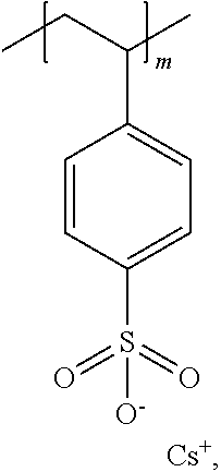
- the cesium salt can be at least one compound selected from the group of structure types consisting of:
- R stands for alkyl (C 1 -C 20 normal, branched, saturated or unsaturated and/or hydroxy-substituted), phenyl (alkylated and/or hydroxy- and/or alkoxy-substituted) and/or pyridyl
- R 1 stands for alkylene (C 2 -C 20 normal, branched, saturated or unsaturated and hydroxy-substituted)
- n and m stand for any commercially available degrees of polymerization of the precursor materials.
- the intermediate layer/the interface which contains the cesium salt, may be applied solution-processed.
- the intermediate layer/the interface containing the cesium salt may be vacuum deposited.
- the intermediate layer/the interface containing the cesium salt may have a thickness in the range between 0.1 nm and 15 nm.
- the structure of the component on a substrate comprised: ITO/PEDOT:PSS (60 nm)/White Polymer (70 nm)/CsSt/Al
- FIG. 1 shows the current-voltage curve
- FIG. 2 shows the luminescence curve
- FIG. 3 shows the efficiency curves
- FIG. 4 shows a further efficiency curve
- a solution-processed organic electronic structural element may comprise a substrate, at least two single-layer or multilayer electrodes, between them at least one active organic semiconductive layer and between an electrode layer and an active organic semiconductive layer an intermediate layer and/or an interface, characterized in that a cesium salt of an organic mono-, oligo- and polycarboxylic or sulfonic acid is contained as an n-dopant in the intermediate layer/the interface.
- an interface is the layered region of two adjacent layers which do not necessarily have to be clearly delimited, in which, according to the surface conditions of the layers in question or for other reasons, the precise material composition has changed, for example, compared to the center of the layer or to the opposing layer surface.
- the application of voltage to both sides of a layer laced with charge carriers causes the charge carriers with a positive charge to migrate to the negative pole and the charge carriers with a negative charge to migrate to the opposite side, while on the other hand, a uniform distribution of the charge carriers will be observed in center of the layer.
- the interface is then denoted as the part of the layer in which an increase in one type of charge carriers is observed.
- R stands for alkyl (C 1 -C 20 normal, branched, saturated or unsaturated and/or hydroxy-substituted), phenyl (alkylated and/or hydroxy- and/or alkoxy-substituted) and/or pyridyl
- R 1 stands for alkylene (C 2 -C 20 normal, branched, saturated or unsaturated and hydroxy-substituted)
- n and m stand for any natural numbers, commercially obtainable degrees of polymerization of the precursor materials, wherein precursor materials should be understood, for example to be free organic polyacids or organic polysulfonic acids.
- polymeric organic electronic components are organic electronic components comprising solution-processed long-chain organic layers.
- Material properties suitable for liquid processes are achieved for example by the length of the alkyl groups. It is also possible to use different solvents.
- the semiconductive organic material can for example be applied from solution, from preferably polar solvents; depending upon the cesium salt used, it can also be vacuum deposited. Application can preferably be performed using the known coating methods such as spin coating, spraying, sputtering etc.
- a lower single-layer or multilayer electrode is applied to a substrate, followed by an organic semiconductive and active layer and finally a layer, in which the use according to an embodiment of cesium salts is implemented.
- the electrode layer is applied to this intermediate layer for better electron injection from a metal electrode such as for example an aluminum electrode.
- the materials are produced by the conversion of the free acids under heating with cesium carbonate in a polar solvent (butanol, ethanol or acetonitrile etc.)
- the layer thickness of the emission layer depends upon the emitter material and is typically less than 15 nm, that is in the range of from 0.1 to 15 nm, in particular less than 10 nm and particularly preferably in the range of 3 to 5 nm.
- Electrode layers can be metal electrode layers, such as, for example, layers made of aluminum, silver, gold, palladium, chromium, zinc, platinum etc and any alloys thereof.
- the component is not in any way inferior compared to the reference with a barium-aluminum electrode, but displays virtually identical current-voltage and luminescence values.
- the various embodiments provide for the first time an alternative to a multilayer electrode using barium in organic electronic components.
- an intermediate layer comprising at least one cesium salt is integrated which makes it possible for the operating voltage and luminescence of the organic component, that is for example of the OLED compared to the OLED with barium as an electron injection layer, to have at least an equivalent efficiency (see Figs. with the characteristic curves).
- the various embodiments describe the use of an alkali metal salt as an n-dopand for doping an organic semiconductive material in order to change the electrical properties of the latter, wherein the alkali metal salt represents an n-dopand with respect to the adjacent materials.
- the various embodiments relate to a solution-processed organic electronic structural element with an improved electrode layer. Located between the active organic layer and the electrode layer there is either an interface or an interlayer, that is an intermediate layer containing a cesium salt.
Abstract
Description
alkane sulfonic acids:
dicarboxylic acids:
disulfonic acids:
polymer-bound carboxylic acids:

and polymer-bound sulfonic acids

wherein R stands for alkyl (C1-C20 normal, branched, saturated or unsaturated and/or hydroxy-substituted), phenyl (alkylated and/or hydroxy- and/or alkoxy-substituted) and/or pyridyl, R1 stands for alkylene (C2-C20 normal, branched, saturated or unsaturated and hydroxy-substituted), 1,2-phenylene, 1,3-phenylene 1,4-phenylene or 2,6-pyridylen, n and m stand for any commercially available degrees of polymerization of the precursor materials. According to another embodiment, the intermediate layer/the interface, which contains the cesium salt, may be applied solution-processed. According to another embodiment, the intermediate layer/the interface containing the cesium salt may be vacuum deposited. According to another embodiment, the intermediate layer/the interface containing the cesium salt may have a thickness in the range between 0.1 nm and 15 nm.
2) Alkane Sulfonic Acids:
3) Dicarboxylic Acids:
4) Disulfonic Acids:
5) Polymer-Bound Carboxylic Acids:

6) Polymer-Bound Sulfonic Acids

wherein R stands for alkyl (C1-C20 normal, branched, saturated or unsaturated and/or hydroxy-substituted), phenyl (alkylated and/or hydroxy- and/or alkoxy-substituted) and/or pyridyl,
R1 stands for alkylene (C2-C20 normal, branched, saturated or unsaturated and hydroxy-substituted), 1,2-phenylene, 1,3-phenylene 1,4-phenylene or 2,6-pyridylene,
n and m stand for any natural numbers, commercially obtainable degrees of polymerization of the precursor materials, wherein precursor materials should be understood, for example to be free organic polyacids or organic polysulfonic acids.


D1b) Imidizing Condensation

d2) Synthesis of the Cesium Salt:
-
- spin coating PEDOT:PSS 60-80 nm on ITO substrate (glass)
- annealing the PEDOT layer
- spin coating an LEP (light-emitting polymer) 70-100 nm
- spin coating the organic cesium salt layer or vapor deposition of the organic-cesium salt layer or vapor deposition of the barium layer
- vapor deposition of the aluminum layer
Claims (11)


Priority Applications (1)
| Application Number | Priority Date | Filing Date | Title |
|---|---|---|---|
| US13/467,594 US9040112B2 (en) | 2007-09-24 | 2012-05-09 | Solution-processed organic electronic structural element with improved electrode layer |
Applications Claiming Priority (5)
| Application Number | Priority Date | Filing Date | Title |
|---|---|---|---|
| DE102007045518A DE102007045518B4 (en) | 2007-09-24 | 2007-09-24 | Solution-processed organic electronic component with improved electrode layer |
| DE102007045518.8 | 2007-09-24 | ||
| DE102007045518 | 2007-09-24 | ||
| US12/234,903 US20090085472A1 (en) | 2007-09-24 | 2008-09-22 | Solution-Processed Organic Electronic Structural Element with Improved Electrode Layer |
| US13/467,594 US9040112B2 (en) | 2007-09-24 | 2012-05-09 | Solution-processed organic electronic structural element with improved electrode layer |
Related Parent Applications (1)
| Application Number | Title | Priority Date | Filing Date |
|---|---|---|---|
| US12/234,903 Continuation US20090085472A1 (en) | 2007-09-24 | 2008-09-22 | Solution-Processed Organic Electronic Structural Element with Improved Electrode Layer |
Publications (2)
| Publication Number | Publication Date |
|---|---|
| US20120220075A1 US20120220075A1 (en) | 2012-08-30 |
| US9040112B2 true US9040112B2 (en) | 2015-05-26 |
Family
ID=39865506
Family Applications (2)
| Application Number | Title | Priority Date | Filing Date |
|---|---|---|---|
| US12/234,903 Abandoned US20090085472A1 (en) | 2007-09-24 | 2008-09-22 | Solution-Processed Organic Electronic Structural Element with Improved Electrode Layer |
| US13/467,594 Expired - Fee Related US9040112B2 (en) | 2007-09-24 | 2012-05-09 | Solution-processed organic electronic structural element with improved electrode layer |
Family Applications Before (1)
| Application Number | Title | Priority Date | Filing Date |
|---|---|---|---|
| US12/234,903 Abandoned US20090085472A1 (en) | 2007-09-24 | 2008-09-22 | Solution-Processed Organic Electronic Structural Element with Improved Electrode Layer |
Country Status (4)
| Country | Link |
|---|---|
| US (2) | US20090085472A1 (en) |
| EP (1) | EP2040317B1 (en) |
| JP (1) | JP5692959B2 (en) |
| DE (1) | DE102007045518B4 (en) |
Cited By (1)
| Publication number | Priority date | Publication date | Assignee | Title |
|---|---|---|---|---|
| US10032983B2 (en) | 2013-05-27 | 2018-07-24 | Merck Patent Gmbh | Electron transfer composition for use in an electron injection layer for organic electronic devices |
Families Citing this family (3)
| Publication number | Priority date | Publication date | Assignee | Title |
|---|---|---|---|---|
| KR101421559B1 (en) | 2010-01-20 | 2014-07-23 | 경북대학교 산학협력단 | Organic devices comprising doped organic semiconductor |
| CN103779498A (en) * | 2014-01-23 | 2014-05-07 | 上海交通大学 | Electron injection method of conductive polymeric materials |
| CN112390908B (en) * | 2019-08-12 | 2022-07-12 | 中国石油化工股份有限公司 | Polymer suspension, method for the production thereof and use thereof |
Citations (20)
| Publication number | Priority date | Publication date | Assignee | Title |
|---|---|---|---|---|
| JPS63230795A (en) | 1987-03-16 | 1988-09-27 | キング、インダストリーズ、インコーポレーテッド | Heat stable sulfonate composition |
| JPH0789928A (en) | 1993-09-28 | 1995-04-04 | Teijin Ltd | Production of aromatic dicarboxylic acid diaryl ester |
| US5965281A (en) | 1997-02-04 | 1999-10-12 | Uniax Corporation | Electrically active polymer compositions and their use in efficient, low operating voltage, polymer light-emitting diodes with air-stable cathodes |
| US6194119B1 (en) * | 1999-01-15 | 2001-02-27 | 3M Innovative Properties Company | Thermal transfer element and process for forming organic electroluminescent devices |
| US20010033347A1 (en) * | 2000-03-17 | 2001-10-25 | Minolta Co., Ltd. | Display element and layered type display element |
| US20030088043A1 (en) * | 2001-06-21 | 2003-05-08 | Wei Huang | Light-emitting polymers and polymer light-emitting diodes |
| JP2003303681A (en) | 2002-04-09 | 2003-10-24 | Sharp Corp | Organic led element and its manufacturing method as well as organic led display device |
| US20030209707A1 (en) | 2002-03-18 | 2003-11-13 | Seiko Epson Corporation | Organic electroluminescent device, method for manufacturing the same, and display unit |
| EP1365633A1 (en) | 2000-12-25 | 2003-11-26 | NEC Corporation | Organic electroluminescence element |
| US20030224203A1 (en) * | 2002-06-03 | 2003-12-04 | Eastman Kodak Company | Organic light-emitting device structure using metal cathode sputtering |
| EP1369937A2 (en) | 2002-06-03 | 2003-12-10 | EASTMAN KODAK COMPANY (a New Jersey corporation) | Sputtered cathode for an organic light-emitting device having an alkali metal compound in the device structure |
| DE10261609A1 (en) | 2002-12-20 | 2004-07-08 | Technische Universität Dresden | Light emitting arrangement |
| JP2004335137A (en) | 2003-04-30 | 2004-11-25 | Canon Inc | Light emitting element |
| WO2005086251A2 (en) | 2004-03-03 | 2005-09-15 | Novaled Gmbh | Use of metal complexes as n-dopants for organic semiconductors and production thereof including their ligands |
| EP1648042A1 (en) | 2004-10-07 | 2006-04-19 | Novaled GmbH | A method for doping a semiconductor material with cesium |
| EP1725080A1 (en) | 2004-03-11 | 2006-11-22 | Idemitsu Kosan Co., Ltd. | Organic electroluminescent device, method for manufacturing same and organic solution |
| JP2007059243A (en) | 2005-08-25 | 2007-03-08 | Konica Minolta Holdings Inc | Organic electroluminescence element, indicating device and lighting device |
| JP2007088015A (en) | 2005-09-20 | 2007-04-05 | Konica Minolta Holdings Inc | Organic electroluminescence element and its manufacturing method |
| FR2892860A1 (en) | 2006-02-28 | 2007-05-04 | Thomson Licensing Sas | Organic diode for e.g. image display sign, has barrier layer placed between organic electroluminescent layer and electron transport layer and with sequestering agents for dopant of electron transport layer |
| WO2007069539A1 (en) | 2005-12-15 | 2007-06-21 | Konica Minolta Holdings, Inc. | Organic electroluminescent device, display and illuminating device |
-
2007
- 2007-09-24 DE DE102007045518A patent/DE102007045518B4/en not_active Expired - Fee Related
-
2008
- 2008-09-19 JP JP2008240682A patent/JP5692959B2/en not_active Expired - Fee Related
- 2008-09-22 US US12/234,903 patent/US20090085472A1/en not_active Abandoned
- 2008-09-22 EP EP08164755.4A patent/EP2040317B1/en not_active Not-in-force
-
2012
- 2012-05-09 US US13/467,594 patent/US9040112B2/en not_active Expired - Fee Related
Patent Citations (25)
| Publication number | Priority date | Publication date | Assignee | Title |
|---|---|---|---|---|
| JPS63230795A (en) | 1987-03-16 | 1988-09-27 | キング、インダストリーズ、インコーポレーテッド | Heat stable sulfonate composition |
| JPH0789928A (en) | 1993-09-28 | 1995-04-04 | Teijin Ltd | Production of aromatic dicarboxylic acid diaryl ester |
| US5965281A (en) | 1997-02-04 | 1999-10-12 | Uniax Corporation | Electrically active polymer compositions and their use in efficient, low operating voltage, polymer light-emitting diodes with air-stable cathodes |
| US6194119B1 (en) * | 1999-01-15 | 2001-02-27 | 3M Innovative Properties Company | Thermal transfer element and process for forming organic electroluminescent devices |
| US20010033347A1 (en) * | 2000-03-17 | 2001-10-25 | Minolta Co., Ltd. | Display element and layered type display element |
| EP1365633A1 (en) | 2000-12-25 | 2003-11-26 | NEC Corporation | Organic electroluminescence element |
| US20030088043A1 (en) * | 2001-06-21 | 2003-05-08 | Wei Huang | Light-emitting polymers and polymer light-emitting diodes |
| US20030209707A1 (en) | 2002-03-18 | 2003-11-13 | Seiko Epson Corporation | Organic electroluminescent device, method for manufacturing the same, and display unit |
| JP2003303681A (en) | 2002-04-09 | 2003-10-24 | Sharp Corp | Organic led element and its manufacturing method as well as organic led display device |
| JP2004014511A (en) | 2002-06-03 | 2004-01-15 | Eastman Kodak Co | Organic light-emitting diode device |
| EP1369937A2 (en) | 2002-06-03 | 2003-12-10 | EASTMAN KODAK COMPANY (a New Jersey corporation) | Sputtered cathode for an organic light-emitting device having an alkali metal compound in the device structure |
| US20030224203A1 (en) * | 2002-06-03 | 2003-12-04 | Eastman Kodak Company | Organic light-emitting device structure using metal cathode sputtering |
| JP2004014512A (en) | 2002-06-03 | 2004-01-15 | Eastman Kodak Co | Organic light emitting diode device |
| EP1369938A2 (en) | 2002-06-03 | 2003-12-10 | Eastman Kodak Company | An organic light-emitting device structure using metal cathode sputtering |
| US20050236973A1 (en) | 2002-12-20 | 2005-10-27 | Karl Leo | Electroluminescent assembly |
| DE10261609A1 (en) | 2002-12-20 | 2004-07-08 | Technische Universität Dresden | Light emitting arrangement |
| JP2004335137A (en) | 2003-04-30 | 2004-11-25 | Canon Inc | Light emitting element |
| WO2005086251A2 (en) | 2004-03-03 | 2005-09-15 | Novaled Gmbh | Use of metal complexes as n-dopants for organic semiconductors and production thereof including their ligands |
| US20090212280A1 (en) | 2004-03-03 | 2009-08-27 | Ansgar Werner | Use of a Metal Complex as an N-Dopant for an Organic Semiconducting Matrix Material, Organic of Semiconducting Material and Electronic Component, and also a Dopant and Ligand and Process for Producing same |
| EP1725080A1 (en) | 2004-03-11 | 2006-11-22 | Idemitsu Kosan Co., Ltd. | Organic electroluminescent device, method for manufacturing same and organic solution |
| EP1648042A1 (en) | 2004-10-07 | 2006-04-19 | Novaled GmbH | A method for doping a semiconductor material with cesium |
| JP2007059243A (en) | 2005-08-25 | 2007-03-08 | Konica Minolta Holdings Inc | Organic electroluminescence element, indicating device and lighting device |
| JP2007088015A (en) | 2005-09-20 | 2007-04-05 | Konica Minolta Holdings Inc | Organic electroluminescence element and its manufacturing method |
| WO2007069539A1 (en) | 2005-12-15 | 2007-06-21 | Konica Minolta Holdings, Inc. | Organic electroluminescent device, display and illuminating device |
| FR2892860A1 (en) | 2006-02-28 | 2007-05-04 | Thomson Licensing Sas | Organic diode for e.g. image display sign, has barrier layer placed between organic electroluminescent layer and electron transport layer and with sequestering agents for dopant of electron transport layer |
Non-Patent Citations (4)
| Title |
|---|
| European Search Report and Written Opinion for Application No. 08164755.4 (7 pages), Aug. 18, 2011. |
| Japanese Office Action, Application No. 2008-240682, 7 pages, Feb. 1, 2013. |
| JP2004-335137 (machine translation), Nov. 25, 2004. * |
| JP2007-088015 (machine translation), Apr. 5, 2007. * |
Cited By (1)
| Publication number | Priority date | Publication date | Assignee | Title |
|---|---|---|---|---|
| US10032983B2 (en) | 2013-05-27 | 2018-07-24 | Merck Patent Gmbh | Electron transfer composition for use in an electron injection layer for organic electronic devices |
Also Published As
| Publication number | Publication date |
|---|---|
| DE102007045518A1 (en) | 2009-04-02 |
| EP2040317A3 (en) | 2011-09-14 |
| US20120220075A1 (en) | 2012-08-30 |
| DE102007045518B4 (en) | 2010-12-16 |
| US20090085472A1 (en) | 2009-04-02 |
| JP5692959B2 (en) | 2015-04-01 |
| JP2009076461A (en) | 2009-04-09 |
| EP2040317A2 (en) | 2009-03-25 |
| EP2040317B1 (en) | 2018-04-04 |
Similar Documents
| Publication | Publication Date | Title |
|---|---|---|
| JP5775902B2 (en) | Polythiophene-containing dispersion | |
| JP5575105B2 (en) | Organic thin film transistor | |
| Wang et al. | Modifying organic/metal interface via solvent treatment to improve electron injection in organic light emitting diodes | |
| US10043869B2 (en) | Method of preparing graphene-based thin-film laminate and graphene-based thin-film laminate prepared using the same | |
| US8053023B2 (en) | Conductive layer and organic electroluminescent device including the same | |
| TWI401291B (en) | Polythiophene formulations for improving organic light emitting diodes | |
| TWI657123B (en) | Perovskite light-emitting device and fabricating method thereof | |
| US20110221061A1 (en) | Anode for an organic electronic device | |
| US20080171228A1 (en) | System for displaying images | |
| Ahn et al. | Impact of Interface Mixing on the Performance of Solution Processed Organic Light Emitting Diodes Impedance and Ultraviolet Photoelectron Spectroscopy Study | |
| Höfle et al. | Charge generation layers for solution processed tandem organic light emitting diodes with regular device architecture | |
| US20130264559A1 (en) | Hole Injection Layers | |
| KR20060041801A (en) | Polythiophene formulations for improving organic light-emitting diodes | |
| US9040112B2 (en) | Solution-processed organic electronic structural element with improved electrode layer | |
| JP6411036B2 (en) | Organic electronic devices | |
| US8269211B2 (en) | Organic electronic device with an organic semiconductor layer | |
| KR20110132165A (en) | EFFICIENT HYBRID ORGANIC·IORGANIC LIGHT EMITTING DIODES WITH SELF-ASSEMBLED DIPOLE MOLECULE DEPOSTITED METAL OXIDE | |
| US10319910B2 (en) | Organic electroluminescent diode and method for manufacturing hole transporting layer thereof | |
| CN102169969A (en) | Anode modification method of organic electroluminescent device | |
| US10658598B2 (en) | Fluorinated aromatic small molecules as functional additives for dispersion of conductive polymers | |
| Yu et al. | An electrochemically deposited film as an interface layer to improve the performance of polymer light-emitting diodes | |
| CN111081904A (en) | Preparation method of graphene oxide film, OLED device and preparation method | |
| JP2011003442A (en) | Method of manufacturing organic thin film element | |
| TWI450429B (en) | Organic thin film transistor and method for preparing thereof | |
| JP2007027130A (en) | Organic electronic device and manufacturing method of same |
Legal Events
| Date | Code | Title | Description |
|---|---|---|---|
| AS | Assignment |
Owner name: OSRAM OPTO SEMICONDUCTORS GMBH, GERMANY Free format text: ASSIGNMENT OF ASSIGNORS INTEREST;ASSIGNORS:KANITZ, ANDREAS;PATZOLD, RALPH;SARFERT, WIEBKE;AND OTHERS;SIGNING DATES FROM 20081022 TO 20081103;REEL/FRAME:028368/0523 |
|
| FEPP | Fee payment procedure |
Free format text: PAYOR NUMBER ASSIGNED (ORIGINAL EVENT CODE: ASPN); ENTITY STATUS OF PATENT OWNER: LARGE ENTITY |
|
| STCF | Information on status: patent grant |
Free format text: PATENTED CASE |
|
| AS | Assignment |
Owner name: OSRAM OLED GMBH, GERMANY Free format text: ASSIGNMENT OF ASSIGNORS INTEREST;ASSIGNOR:OSRAM OPTO SEMICONDUCTORS GMBH;REEL/FRAME:036805/0402 Effective date: 20150619 |
|
| FEPP | Fee payment procedure |
Free format text: MAINTENANCE FEE REMINDER MAILED (ORIGINAL EVENT CODE: REM.); ENTITY STATUS OF PATENT OWNER: LARGE ENTITY |
|
| LAPS | Lapse for failure to pay maintenance fees |
Free format text: PATENT EXPIRED FOR FAILURE TO PAY MAINTENANCE FEES (ORIGINAL EVENT CODE: EXP.); ENTITY STATUS OF PATENT OWNER: LARGE ENTITY |
|
| STCH | Information on status: patent discontinuation |
Free format text: PATENT EXPIRED DUE TO NONPAYMENT OF MAINTENANCE FEES UNDER 37 CFR 1.362 |
|
| FP | Lapsed due to failure to pay maintenance fee |
Effective date: 20190526 |