US9037625B2 - Multi-standard multi-rate filter - Google Patents

Multi-standard multi-rate filter Download PDF

Info

Publication number
US9037625B2
US9037625B2 US13/441,501 US201213441501A US9037625B2 US 9037625 B2 US9037625 B2 US 9037625B2 US 201213441501 A US201213441501 A US 201213441501A US 9037625 B2 US9037625 B2 US 9037625B2
Authority
US
United States
Prior art keywords
filter
allpass
iir filters
factor
filters
Prior art date
Legal status (The legal status is an assumption and is not a legal conclusion. Google has not performed a legal analysis and makes no representation as to the accuracy of the status listed.)
Expired - Fee Related, expires
Application number
US13/441,501
Other versions
US20120254272A1 (en
Inventor
Mark Alan Sturza
Donald Leimer
Current Assignee (The listed assignees may be inaccurate. Google has not performed a legal analysis and makes no representation or warranty as to the accuracy of the list.)
CSR Technology Inc
Original Assignee
CSR Technology Inc
Priority date (The priority date is an assumption and is not a legal conclusion. Google has not performed a legal analysis and makes no representation as to the accuracy of the date listed.)
Filing date
Publication date
Application filed by CSR Technology Inc filed Critical CSR Technology Inc
Priority to US13/441,501 priority Critical patent/US9037625B2/en
Assigned to SIRF TECHNOLOGY, INC. reassignment SIRF TECHNOLOGY, INC. ASSIGNMENT OF ASSIGNORS INTEREST (SEE DOCUMENT FOR DETAILS). Assignors: STURZA, MARK ALAN, LEIMER, DONALD
Publication of US20120254272A1 publication Critical patent/US20120254272A1/en
Assigned to CSR Technology, Inc. reassignment CSR Technology, Inc. CHANGE OF NAME (SEE DOCUMENT FOR DETAILS). Assignors: SIRF TECHNOLOGY, INC.
Application granted granted Critical
Publication of US9037625B2 publication Critical patent/US9037625B2/en
Expired - Fee Related legal-status Critical Current
Adjusted expiration legal-status Critical

Links

Images

Classifications

    • HELECTRICITY
    • H03ELECTRONIC CIRCUITRY
    • H03HIMPEDANCE NETWORKS, e.g. RESONANT CIRCUITS; RESONATORS
    • H03H17/00Networks using digital techniques
    • H03H17/02Frequency selective networks
    • H03H17/0248Filters characterised by a particular frequency response or filtering method
    • H03H17/0264Filter sets with mutual related characteristics
    • H03H17/0273Polyphase filters
    • H03H17/0277Polyphase filters comprising recursive filters
    • H03H17/0279Polyphase filters comprising recursive filters having two phases
    • HELECTRICITY
    • H03ELECTRONIC CIRCUITRY
    • H03HIMPEDANCE NETWORKS, e.g. RESONANT CIRCUITS; RESONATORS
    • H03H17/00Networks using digital techniques
    • H03H17/02Frequency selective networks
    • H03H17/0248Filters characterised by a particular frequency response or filtering method
    • H03H17/0264Filter sets with mutual related characteristics
    • H03H17/0273Polyphase filters
    • H03H17/0277Polyphase filters comprising recursive filters
    • HELECTRICITY
    • H03ELECTRONIC CIRCUITRY
    • H03HIMPEDANCE NETWORKS, e.g. RESONANT CIRCUITS; RESONATORS
    • H03H17/00Networks using digital techniques
    • H03H17/02Frequency selective networks
    • H03H17/06Non-recursive filters
    • H03H17/0621Non-recursive filters with input-sampling frequency and output-delivery frequency which differ, e.g. extrapolation; Anti-aliasing
    • H03H17/0635Non-recursive filters with input-sampling frequency and output-delivery frequency which differ, e.g. extrapolation; Anti-aliasing characterized by the ratio between the input-sampling and output-delivery frequencies
    • H03H17/065Non-recursive filters with input-sampling frequency and output-delivery frequency which differ, e.g. extrapolation; Anti-aliasing characterized by the ratio between the input-sampling and output-delivery frequencies the ratio being integer
    • H03H17/0664Non-recursive filters with input-sampling frequency and output-delivery frequency which differ, e.g. extrapolation; Anti-aliasing characterized by the ratio between the input-sampling and output-delivery frequencies the ratio being integer where the output-delivery frequency is lower than the input sampling frequency, i.e. decimation

Definitions

  • the present invention relates to a high-performance; small die size, and low-power dissipation decimation filter.
  • FIR filters finite impulse response filters or infinite impulse response (IIR) filters.
  • IIR filters require large numbers of coefficients to meet the transition band and stopband attenuation requirements. Further, multiple sets of these coefficients are required to support the various coding standards and channel bandwidths. As a result, a large on-chip memory is required.
  • IIR filters also require many sections to meet such requirements and are sensitive to both coefficient and signal quantization.
  • a method for decimating a digital signal by a factor of M and matching it to a desired channel bandwidth.
  • the method applies the digital signal input samples to a (M ⁇ 1) stage tapped delay line, downsamples the input samples and the output samples of each tapped delay line stage by a factor of M, and applies each of the M downsampled sample value streams to M allpass HR filters, respectively.
  • the M allpass IIR filtered sample streams are then summed and scaled by a factor of 1/M. The result can then be filtered by a digital channel filter.
  • FIG. 1 shows a functional block diagram of a zero-IF/very low-IF (ZIF/VLIF) radio receiver front-end 100 .
  • ZIF/VLIF zero-IF/very low-IF
  • FIG. 2 is a graph illustrating aspects of the filter requirements in relation to the components of the ZIF/VL1F radio front-end.
  • FIG. 3 is a functional block diagram of IF sampling radio receiver front-end 300 , in accordance with an alternate embodiment of the present invention.
  • FIG. 4 shows an example of an M-path polyphase IIR decimate-by-M filter structure 400 .
  • FIG. 5 shows half-band, 2-path polyphase IIR decimator structure 500 configured in accordance with one embodiment of the present invention.
  • FIG. 6 shows third-band, 3-path polyphase IIR decimator structure 600 , configured in accordance with one embodiment of the present invention.
  • FIG. 7 shows generalized 2-path polyphase IIR filter structure 700 , configured in accordance with one embodiment of the present invention.
  • FIG. 8 shows respective 1-coefficient (“real”) section and a 2-coefficient (“complex”) section IIR allpass filter structures 800 and 850 , respectively, configured in accordance with embodiments of the present invention.
  • FIG. 9 shows 3-coefficient filter 900 which is formed by cascading 3 real sections.
  • FIG. 10 illustrates quad-ratio (2, 3, 4, and 6) decimator multi-standard filter 1000 , configured in accordance with one embodiment of the present invention.
  • FIG. 11 illustrates quad-ratio (2, 3, 4, and 6) multi-standard decimator structure 1100 , configured in accordance with yet a further embodiment of the present invention.
  • FIG. 12 shows an example of the allpass filter sections of H 1 filter 1101 of FIG. 11 , configured in accordance with the present invention.
  • FIG. 13 shows an example of the allpass filter sections 1106 , 1107 and 1108 of H 2 filter 1102 , configured in accordance with the present invention.
  • FIG. 14 shows an example of the allpass filter sections 1109 , 1110 and 1111 of H 3 filter 1102 , configured in accordance with the present invention.
  • the present invention provides a multi-standard, multi-ratio decimator with improved performance at a lower cost (e.g., smaller die size) and a lower DC power dissipation than was achieved in previously available decimators.
  • a quad-ratio e.g., 2, 3, 4, and 6
  • multi-standard e.g., DVB-T/H, ISDB-T and T-DAB
  • the present multi-standard, multi-rate filter trades-off power dissipation with performance. Decreasing the sampling rate reduces power dissipation at the expense of increased aliasing distortion. If the adjacent channel interference (ACI) is small, this added distortion may be acceptable.
  • the sampling rate can be adjusted to a smaller multiple of the orthogonal frequency division multiplexing (OFDM) fast Fourier transform (FFT) sampling rate when the ACI is low, and increased to a higher multiple when the ACI is high. In this way power dissipation is reduced, when possible, without performance degradation.
  • OFDM orthogonal frequency division multiplexing
  • FFT fast Fourier transform
  • FIG. 1 a functional block diagram of zero-IF/very low-IF (ZIF/VLIF) radio receiver front-end 100 is shown.
  • Multi-standard, multi-rate filters which are configured in accordance with embodiments of the present invention are provided as the final blocks 101 and 102 of the in-phase (I) and quadrature-phase (Q) paths, respectively.
  • the multi-standard, multirate filters 101 and 102 each have transfer function H(z) and decimation ratio M.
  • signal F RF denotes the input RF signal applied to mixers 103 and 104 for the I and Q paths, respectively.
  • Mixers 103 and 104 also receive as inputs the output signal of voltage controlled oscillator (VCO) 105 of frequency F VCO .
  • VCO voltage controlled oscillator
  • VCO 105 VCO 105 's signal received at mixer 104 in the Q path is phase-shifted from that received at mixer 103 in the I path by ⁇ /2.
  • the output signals of mixers 103 and 104 are applied as input signals to analog low pass filters (LPF) 107 and 108 each of bandwidth B LP .
  • LPF analog low pass filters
  • the output signals of LPFs 107 and 108 are capacitivly coupled to input signals of analog-to-digital (A/D) converters 109 and 110 to remove DC offsets.
  • the A/D converters sample and quantize their input signals at a sampling rate of F S .
  • the resulting sampled and quantized signals are digitally filtered and decimated by multi-standard, multi-rate filters 101 and 102 to provide the respective I(k) and Q(k) output signals.
  • FIG. 2 is a graph illustrating various aspects of the filter requirements in relation to other components of the ZIF/VLIF radio.
  • frequency F PB denotes the passband bandwidth
  • frequency F SB is the frequency at the high frequency edge of the stop-band
  • frequency F S is the A/D sampling rate
  • amplitude A PB is the allowable passband ripple
  • amplitude A SB is the required stopband attenuation.
  • FIG. 3 is a functional block diagram of IF sampling radio receiver front-end 300 , in accordance with an alternate embodiment of the present invention.
  • multi-standard multi-rate filters 301 and 302 are the final blocks of the in-phase (I) and quadrature-phase (Q) paths, each having transfer function H(z) and decimation ratio M.
  • an input IF signal of frequency F IF e.g., 36 MHz, 36.125 MHz, and 36.17 MHz
  • BPF IF bandpass filter
  • the resulting bandpass signal is capacitivly coupled to A/D converter (of sample rate F s ) 304 to remove DC offsets.
  • A/D converter 304 samples and quantizes the bandpass signal of bandpass filter 303 , and provides as input samples to digital mixers 305 and 306 of the I and Q paths.
  • digital mixers 305 and 306 each also receive as an input digital signal an output digital signal of numerically controlled oscillator (NCO) 307 , which receives a digital word F NCO , representing the NCO frequency.
  • NCO 307 's output signal to the Q path mixer 306 is phase-shifted by ⁇ /2 from that of the input signal to mixer 305 of the I path.
  • the sampled and quantized IF samples are thus multiplied by the sine and cosine of NCO 307 's output phase, respectively.
  • the resulting samples are digitally filtered, and decimated by multi-standard, multi-rate filters 301 and 302 to provide the baseband samples.
  • Digital M-path polyphase infinite impulse response (IIR) filters are suitable for use in decimators with decimation ratio M, for M greater than 1.
  • the M-path polyphase IIR filters are based on an M-tap finite impute response (FIR) filter in which the coefficients are replaced by allpass filters.
  • Polyphase IIR filters provide high stopband attenuation and low passband ripple with a relatively small number of coefficients.
  • FIG. 4 shows an example of an M-path polyphase IIR decimate-by-M filter structure 400 .
  • input sample x(n) is applied to an M ⁇ 1 stage, tapped delay line.
  • the input sample and the output signals of the M ⁇ 1 delay line taps are each downsampled by a factor of M.
  • the M downsampled values are input signals to M allpass filters 401 - 0 , 401 - 1 , . . . , 401 -( m ⁇ 1).
  • the filter output signals are summed in summer 402 and scaled by 1/M scaler 403 to provide output samples y(m).
  • the transfer function of the M-path polyphase IIR decimator 400 is given by:
  • the total number of filter coefficients in this example is M ⁇ N.
  • FIG. 5 shows a half-band, 2-path polyphase IIR decimator structure 500 , configured in accordance with one embodiment of the present invention.
  • input samples x(n) are decimated by 2 and applied as input samples to allpass filter 501 .
  • the input samples are delayed by one sample, decimated by 2, and applied as input samples to allpass filter 502 .
  • Output signals of filters 501 and 502 are summed in summer 503 and scaled by 1 ⁇ 2 at scaler 504 to provide the output samples y(n).
  • FIG. 6 shows third-band, 3-path polyphase IIR decimator structure 600 , configured in accordance with one embodiment of the present invention.
  • input samples x(n) are decimated by 3 and applied to allpass filter 601 .
  • the input samples are also delayed by one sample, decimated by 3, and applied to allpass filter 602 .
  • the input samples are delayed by two samples, decimated by 3, and applied to allpass filter 603 .
  • the filter outputs of allpass filters 601 - 603 are then added together by summer 604 and scaled by 1 ⁇ 3 to form output samples y(n).
  • FIG. 7 shows generalized 2-path polyphase IIR filter structure 700 , configured in accordance with one embodiment of the present invention.
  • input samples x(n) are applied to allpass filter 701 , and filtered by P filter 703 .
  • the filtered samples are applied as input samples to allpass filter 702 .
  • the filtered output samples of allpass filters 701 and 702 are added together in summer 702 and scaled by 1 ⁇ 2in scaler 705 to provide output samples y(n).
  • FIG. 8 shows 1-coefficient (“real section”) and a 2-coefficient (“complex section”) IIR allpass filter structures 800 and 850 , respectively, configured in accordance with embodiments of the present invention.
  • 1-coefficient filter 800 the input samples are delayed in element 802 by one sample and added in summer 801 to a scaled difference (by ⁇ ) between the input samples and samples fed back from the output of IIR allpass filter 800 .
  • the samples fed back from the output of IIR allpass filter 800 are delayed in element 803 by one sample.
  • the input samples are delayed two samples, and summed in summer 855 with the output samples of scaling element (by ⁇ ) 853 and the output samples of scaling element (by ⁇ ) 854 to provide the filter output samples.
  • the input samples to scaling element 853 are the differences between the input samples of the 2-coefficient filter 850 and the output samples of the filter, delayed by two samples.
  • the input samples to scaling elements 854 are the differences between the output samples of the 2-coefficient filter, delayed one sample, and the input samples of 2-coefficient filter 850 , delayed one sample.
  • FIG. 9 shows 3-coefficient filter 900 which is formed by cascading three real sections.
  • delay elements e.g., delay elements 903 and 905 .
  • FIG. 10 illustrates quad-ratio (2, 3, 4, and 6) decimator multi-standard filter 1000 , configured in accordance with one embodiment of the present invention.
  • filter 1000 has an input sample rate of F S and an output sample rate which is selectable between F S /2, F S /3, F S /4, and F S /6, depending on the path selections through the filter structure.
  • the input samples pass through filter 1001 (labeled “H 1 ”), bypass decimation by 2 filter 1005 , pass through the filter 1003 (labeled “H 2 D3 ”, with associated decimation by 3), and pass through filter 1004 (labeled “H 3 ”).
  • the input samples pass through filter 1001 , decimation by 2 filter 1005 , filter 1003 (with its associated decimation by 2), and filter 1004 .
  • the input samples pass through filter 1001 and decimation by 2 filter 1004 , filter 1002 (with its associated decimation by 3), and filter 1004 .
  • Table 1 shows examples of filters parameters for a multi-standard, multi-rate filter with component transfer functions H 1 , H 2 D2 , H 2 D3 , H 3 DVB-T , H 3 ISDB-T and H 3 T-DMB , configured in accordance with the present invention, for supporting DVB-T (also DVB-H, labeled “H 3 DVB-T ”), ISDB-T (labeled “H 3 ISDB-T ”), and T-DAB (also T-DMB, labeled “H 3 T-DMB ”) applications.
  • DVB-T also DVB-H, labeled “H 3 DVB-T ”
  • ISDB-T labeled “H 3 ISDB-T ”
  • T-DAB also T-DMB, labeled “H 3 T-DMB ”
  • frequency F PB denotes the pass-band bandwidth
  • frequency F SB denotes the high-frequency edge of the stop-band
  • F S denotes the A/D sampling rate.
  • Table 2 shows quantized filter coefficients that satisfy the requirements shown in
  • Table 1 expressed as hexadecimal fractions and represent various choices of such coefficients for a multi-standard multi-rate filter configured in accordance with the present invention.
  • a i denotes the transfer function of the IIR filter in the ith path, and each transfer function Ai may be implemented by multiple coefficients.
  • FIG. 11 illustrates quad-ratio (2, 3, 4, and 6) multi-standard decimator structure 1100 , configured in accordance with yet a further embodiment the present invention.
  • FIG. 11 represents replacing each of the H 1 , H 2 , and H 3 filter blocks in FIG. 10 with the appropriate structure from FIG. 4 , FIG. 5 and FIG. 6 , with all adder outputs truncated to 16-bits, and all paths scaled to ⁇ 1 except for the paths labeled ( 2 ), which are scaled to ⁇ 2, and the paths labeled ( 3 ), which are scaled to ⁇ 4.
  • FIG. 12 shows an example of the allpass filter sections 1104 and 1105 of H 1 filter 1101 of FIG. 11 , configured in accordance with the present invention.
  • the adder outputs are truncated to 16-bits and the paths are scaled to ⁇ 1 except for the paths labeled ( 2 ), which are scaled to ⁇ 2.
  • FIG. 13 shows an example of the allpass filter sections 1106 , 1107 and 1108 of the H 2 filter 1102 (i.e., H 2 D2 and H 2 D3 filters), configured in accordance with the present invention.
  • the adder outputs are truncated to 16-bits, and the paths are scaled to ⁇ 1, except for the inputs and outputs of each of the scaling elements ⁇ nm (n running from 0 to 2 and in running from 1 to 3), which are scaled to ⁇ 2.
  • FIG. 14 shows an example of the allpass filter sections 1109 , 1110 and 1111 of the H 3 filter 1102 (i.e., H 3 DVB-T , H 3 ISDB-T , and H 3 T-DAB filters), configured in accordance with the present invention.
  • the adder outputs are truncated to 16-bits and most paths are scaled to ⁇ 2 (as shown by the associated legends), except for those scaled to ⁇ 1 or to ⁇ 4, as indicated.
  • receiver front-end 100 processes broadcast digital multimedia signals in VHF and UHF bands. In the broadcasting community, these frequencies are often referred to as Band I, Band II, Band III, Band IV, Band V, and L-Band.
  • Receiver front-end 100 is designed for the DVB-T/H, ISDB-T, and T-DAB broadcast digital multimedia standards, each of which uses an OFDM modulation.
  • the DVB-T/H channels are 5, 6, 7, and 8 MHz.
  • the ISDB-T channels are 6, 7, and 8 MHz.
  • the T-DAB channels are approximately 1.7 MHz.
  • the receiver front-end By supporting T-DAB, the receiver front-end also supports the T-DMB standard.
  • Receiver front-end 100 converts RF signals into quantized digital samples with minimal degradation.
  • the RF signal is mixed with in-phase and quadrature-phase local oscillator signals from VCO 105 where the difference between the RF frequency and the VCO frequency is either zero (ZIF) or very small (VLIF).
  • the output signals of mixers 103 and 1014 are each lowpass filtered by LPFs 107 and 108 to eliminate the higher frequency sum components, leaving the ZIF or VLIF components.
  • the lowpass bandwidth (B LP ) for LPF 107 and 108 may be selected to be significantly larger than required by the signal bandwidth.
  • the minimum lowpass bandwidth is one-half of the maximum channel bandwidth (e.g., 4-MHz for an 8-MHz channel).
  • One suitable lowpass filter has a 60-dB bandwidth of 11.5 MHz.
  • the filtered signals are capacitively coupled to A/D converters 109 and 110 to remove any DC offset.
  • A/D converters 109 and 110 sample and quantize the signal at sampling rate F S .
  • the sampling rate should be sufficiently high to prevent aliasing, and be an integer multiple M of the OFDM signals' FFT sampling rates. Approximate sampling rates and integer multiples are shown in Table 3 for an 11.5 MHz B LP .
  • decimators 101 and 102 After the signals are sampled and quantized at A/D converters 109 and 110 , the samples are filtered and decimated by decimators 101 and 102 to obtain samples at the OFDM FFT sampling rate with minimal distortion.
  • Decimators 101 and 102 each have a filter transfer function H(z) and decimate by a factor of M.
  • Quad-ratio (2, 3, 4, and 6), multi-standard (DVB-T/H, ISDB-T, and T-DAB) decimator (QRMSD) 1100 of FIG. 11 is a suitable filter for implementing each of decimator 101 and 102 of FIG. 1 .
  • QRMSD 1100 is also a suitable filter for implementing QRMSD filters 301 and 302 of FIG. 3 .
  • decimator 1100 is formed by cascading three filters 1101 , 1102 and 1103 , having transfer functions H 1 , H 2 , and H 3 , respectively. In some configurations, only one or two of the three filters are required.
  • transfer function H 1 can be configured as a half-band, decimate by 2 filter (H 1 D2 ), or as a low-pass filter (LPF) H 1 , by switching in, or out, additional delay elements without changing the coefficients.
  • Transfer function H 2 can be configured as either a half-band, decimate by 2 filter (H 2 D2 ), or as a third-band, decimate by 3, filter (H 2 D3 ), by changing the coefficients.
  • Transfer function H 3 can be configured as any one of a DVB-T LPF, H 3 DVB-T , an ISDB-T LPF, H 3 ISDB-T , or a T-DAB LPF, H 3 T-DAB , by changing the coefficients.
  • the H 2 filter may be designed to meet the DVB-T requirements, which are again more stringent then those for the ISDB-T and T-DAB standards. In that manner, the same H 2 filter may be used for all three standards.
  • only one H 2 D2 and one H 2 D3 filter are required for all three standards and all decimation ratios 2, 3, 4, and 6.
  • the H3 stop-band rejection filters are substantially identical for all decimation ratios.

Abstract

A method is provided for decimating a digital signal by a factor of M and matching it to a desired channel bandwidth. The method applies the digital signal input samples to a (M−1) stage tapped delay line, downsamples the input samples and the output samples of each tapped delay line stage by a factor of M, and applies each of the M downsampled sample value streams to M allpass IIR filters, respectively. The M allpass IIR filtered sample streams are then summed and scaled by a factor of 1/M. The result can then be filtered by a digital channel filter.

Description

CROSS-REFERENCE TO RELATED APPLICATIONS
The present patent application is a continuation of U.S. patent application Ser. No. 11/611,542, filed on Dec. 15, 2006 now U.S. Pat. No. 8,176,107, which application is related to and claims priority of (a) U.S. Provisional Patent Application, entitled “Multi-Standard Multi-Rate Filter,” Ser. No. 60/751,437, filed 16 Dec. 2005; and (b) U.S. Provisional Patent Application, entitled “Differential Evolution Design Of Polyphase IIR Decimation Filters,” Ser. No. 60/752,619 and filed on 20 Dec. 2005. Each of the foregoing applications is hereby incorporated by reference in its entirety into the present application.
BACKGROUND OF THE INVENTION
1. Field of the Invention
The present invention relates to a high-performance; small die size, and low-power dissipation decimation filter.
2. Discussion of the Related Art
Conventional analog filter solutions require switching between different filters or different filter components when processing information coded according to different standards or different channel bandwidths. For analog filters to achieve the required narrow transition bandwidths and high stopband attenuations, precise component tolerances are required. Precise component tolerances are difficult to achieve on-chip, necessitating the use of off-chip components, thereby resulting in increased system cost. Additionally, temperature compensation and aging are also often required.
Conventional digital filter approaches use finite impulse response (FIR) filters or infinite impulse response (IIR) filters. Conventional FIR filters require large numbers of coefficients to meet the transition band and stopband attenuation requirements. Further, multiple sets of these coefficients are required to support the various coding standards and channel bandwidths. As a result, a large on-chip memory is required. Conventional IIR filters also require many sections to meet such requirements and are sensitive to both coefficient and signal quantization.
For a detailed description of the theory and design of FIR digital filters, see Alan Oppenheimer and Ronald Schafer, Digital Signal Processing (Prentice-Hall 1975), especially chapters 5 and 6. Further information regarding conventional filter design may also be found in:
    • a Lutovac, M. D. and Milic, L. D., “Design of High-Speed IIR Filters Based on Elliptic Minimal Q-Factors Prototype” (“Lutovac and Milic”), Conf. ETRAN 2002, Banja Vrucica, pp. 103-106 (2002).
    • b Lutovac, M. D., Tosic, D. V., and Evans, B. L., “Filter Design for Signal Processing—Using MATLAB and Mathematica”, Prentice Hall (2001).
    • c Harris, F. J., “Multirate Signal Processing—For Communication Systems”, Prentice Hall (2004).
    • d Krukowski, A. and Kale, I., “DSP System Design—Complexity Reduced IIR Filter Implementation for Practical Applications” (“Krukowski and Kale”), Kluwer Academic Publishers (2003).
    • e Storn, Rainer, “Designing Nonstandard Filters with Differential Evolution” (“Storn”), IEEE SIGNAL PROCESSING MAGAZINE, January 2005.
SUMMARY
According to one embodiment of the present invention, a method is provided for decimating a digital signal by a factor of M and matching it to a desired channel bandwidth. The method applies the digital signal input samples to a (M−1) stage tapped delay line, downsamples the input samples and the output samples of each tapped delay line stage by a factor of M, and applies each of the M downsampled sample value streams to M allpass HR filters, respectively. The M allpass IIR filtered sample streams are then summed and scaled by a factor of 1/M. The result can then be filtered by a digital channel filter.
The present invention is better understood upon consideration of the detailed description below and the accompanying drawings.
BRIEF DESCRIPTION OF THE DRAWINGS
FIG. 1 shows a functional block diagram of a zero-IF/very low-IF (ZIF/VLIF) radio receiver front-end 100.
FIG. 2 is a graph illustrating aspects of the filter requirements in relation to the components of the ZIF/VL1F radio front-end.
FIG. 3 is a functional block diagram of IF sampling radio receiver front-end 300, in accordance with an alternate embodiment of the present invention.
FIG. 4 shows an example of an M-path polyphase IIR decimate-by-M filter structure 400.
FIG. 5 shows half-band, 2-path polyphase IIR decimator structure 500 configured in accordance with one embodiment of the present invention.
FIG. 6 shows third-band, 3-path polyphase IIR decimator structure 600, configured in accordance with one embodiment of the present invention.
FIG. 7 shows generalized 2-path polyphase IIR filter structure 700, configured in accordance with one embodiment of the present invention.
FIG. 8 shows respective 1-coefficient (“real”) section and a 2-coefficient (“complex”) section IIR allpass filter structures 800 and 850, respectively, configured in accordance with embodiments of the present invention.
FIG. 9 shows 3-coefficient filter 900 which is formed by cascading 3 real sections.
FIG. 10 illustrates quad-ratio (2, 3, 4, and 6) decimator multi-standard filter 1000, configured in accordance with one embodiment of the present invention.
FIG. 11 illustrates quad-ratio (2, 3, 4, and 6) multi-standard decimator structure 1100, configured in accordance with yet a further embodiment of the present invention.
FIG. 12 shows an example of the allpass filter sections of H1 filter 1101 of FIG. 11, configured in accordance with the present invention.
FIG. 13 shows an example of the allpass filter sections 1106, 1107 and 1108 of H2 filter 1102, configured in accordance with the present invention.
FIG. 14 shows an example of the allpass filter sections 1109, 1110 and 1111 of H3 filter 1102, configured in accordance with the present invention.
DETAILED DESCRIPTION OF THE PREFERRED EMBODIMENTS
In exemplary embodiments, the present invention provides a multi-standard, multi-ratio decimator with improved performance at a lower cost (e.g., smaller die size) and a lower DC power dissipation than was achieved in previously available decimators. In one such embodiment, a quad-ratio (e.g., 2, 3, 4, and 6), multi-standard (e.g., DVB-T/H, ISDB-T and T-DAB) decimator that provides excellent performance with a minimal number of logic gates and low DC power dissipation is provided.
The present multi-standard, multi-rate filter trades-off power dissipation with performance. Decreasing the sampling rate reduces power dissipation at the expense of increased aliasing distortion. If the adjacent channel interference (ACI) is small, this added distortion may be acceptable. For example, the sampling rate can be adjusted to a smaller multiple of the orthogonal frequency division multiplexing (OFDM) fast Fourier transform (FFT) sampling rate when the ACI is low, and increased to a higher multiple when the ACI is high. In this way power dissipation is reduced, when possible, without performance degradation.
Referring now to FIG. 1, a functional block diagram of zero-IF/very low-IF (ZIF/VLIF) radio receiver front-end 100 is shown. Multi-standard, multi-rate filters which are configured in accordance with embodiments of the present invention are provided as the final blocks 101 and 102 of the in-phase (I) and quadrature-phase (Q) paths, respectively. The multi-standard, multirate filters 101 and 102 each have transfer function H(z) and decimation ratio M. As shown in FIG. 1, signal FRF denotes the input RF signal applied to mixers 103 and 104 for the I and Q paths, respectively. Mixers 103 and 104 also receive as inputs the output signal of voltage controlled oscillator (VCO) 105 of frequency FVCO. VCO 105's signal received at mixer 104 in the Q path is phase-shifted from that received at mixer 103 in the I path by π/2. The output signals of mixers 103 and 104 are applied as input signals to analog low pass filters (LPF) 107 and 108 each of bandwidth BLP. Thus, the input RF signal is downconverted to zero 1E, or very-low IF.
The output signals of LPFs 107 and 108 are capacitivly coupled to input signals of analog-to-digital (A/D) converters 109 and 110 to remove DC offsets. The A/D converters sample and quantize their input signals at a sampling rate of FS. The resulting sampled and quantized signals are digitally filtered and decimated by multi-standard, multi-rate filters 101 and 102 to provide the respective I(k) and Q(k) output signals.
FIG. 2 is a graph illustrating various aspects of the filter requirements in relation to other components of the ZIF/VLIF radio. As shown in FIG. 2, frequency FPB denotes the passband bandwidth, frequency FSB is the frequency at the high frequency edge of the stop-band, and frequency FS is the A/D sampling rate, amplitude APB is the allowable passband ripple, and amplitude ASB is the required stopband attenuation.
FIG. 3 is a functional block diagram of IF sampling radio receiver front-end 300, in accordance with an alternate embodiment of the present invention. As shown in FIG. 3, multi-standard multi-rate filters 301 and 302 are the final blocks of the in-phase (I) and quadrature-phase (Q) paths, each having transfer function H(z) and decimation ratio M. In this embodiment, an input IF signal of frequency FIF (e.g., 36 MHz, 36.125 MHz, and 36.17 MHz) is applied to an IF bandpass filter (BPF) 303 of bandwidth BBP. The resulting bandpass signal is capacitivly coupled to A/D converter (of sample rate Fs) 304 to remove DC offsets.
A/D converter 304 samples and quantizes the bandpass signal of bandpass filter 303, and provides as input samples to digital mixers 305 and 306 of the I and Q paths. In this case, digital mixers 305 and 306 each also receive as an input digital signal an output digital signal of numerically controlled oscillator (NCO) 307, which receives a digital word FNCO, representing the NCO frequency. As in IF sampling receiver 100, NCO 307's output signal to the Q path mixer 306 is phase-shifted by π/2 from that of the input signal to mixer 305 of the I path. The sampled and quantized IF samples are thus multiplied by the sine and cosine of NCO 307's output phase, respectively. The resulting samples are digitally filtered, and decimated by multi-standard, multi-rate filters 301 and 302 to provide the baseband samples.
Digital M-path polyphase infinite impulse response (IIR) filters are suitable for use in decimators with decimation ratio M, for M greater than 1. The M-path polyphase IIR filters are based on an M-tap finite impute response (FIR) filter in which the coefficients are replaced by allpass filters. Polyphase IIR filters provide high stopband attenuation and low passband ripple with a relatively small number of coefficients.
FIG. 4 shows an example of an M-path polyphase IIR decimate-by-M filter structure 400. As shown in FIG. 4, input sample x(n) is applied to an M−1 stage, tapped delay line. The input sample and the output signals of the M−1 delay line taps are each downsampled by a factor of M. The M downsampled values are input signals to M allpass filters 401-0, 401-1, . . . , 401-(m−1). The filter output signals are summed in summer 402 and scaled by 1/M scaler 403 to provide output samples y(m). The transfer function of the M-path polyphase IIR decimator 400 is given by:
H ( z ) = 1 M k = 0 M z - k A k ( z M )
Assuming that each of the M allpass filters 401-0, 401-1, . . . , 401-(m−1) has N cascaded real sections (i.e. N coefficients), the transfer functions of the allpass filters 401-0, 401-1, . . . , 401-(m−1) each have the form:
A k ( z ) = j = 1 N β k , j + z - 1 1 + β k , j z - 1
Substituting the allpass filter transfer functions into the M-path polyphase IIR decimator 400's transfer function then gives:
H ( z ) = 1 M k = 0 M z - k j = 1 N β k , j + z - M 1 + β k , j z - M
Thus, the total number of filter coefficients in this example is M×N.
To illustrate some of the polyphase IIR decimators of the present invention, FIG. 5 shows a half-band, 2-path polyphase IIR decimator structure 500, configured in accordance with one embodiment of the present invention. As shown in FIG. 5, input samples x(n) are decimated by 2 and applied as input samples to allpass filter 501. Concurrently, the input samples are delayed by one sample, decimated by 2, and applied as input samples to allpass filter 502. Output signals of filters 501 and 502 are summed in summer 503 and scaled by ½ at scaler 504 to provide the output samples y(n).
Similarly, FIG. 6 shows third-band, 3-path polyphase IIR decimator structure 600, configured in accordance with one embodiment of the present invention. As shown in FIG. 6, input samples x(n) are decimated by 3 and applied to allpass filter 601. The input samples are also delayed by one sample, decimated by 3, and applied to allpass filter 602. Further, the input samples are delayed by two samples, decimated by 3, and applied to allpass filter 603. The filter outputs of allpass filters 601-603 are then added together by summer 604 and scaled by ⅓ to form output samples y(n).
FIG. 7 shows generalized 2-path polyphase IIR filter structure 700, configured in accordance with one embodiment of the present invention. As shown in FIG. 7, input samples x(n) are applied to allpass filter 701, and filtered by P filter 703. The filtered samples are applied as input samples to allpass filter 702. The filtered output samples of allpass filters 701 and 702 are added together in summer 702 and scaled by ½in scaler 705 to provide output samples y(n).
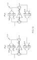
To illustrate the transfer function of the allpass filters of the present invention, FIG. 8 shows 1-coefficient (“real section”) and a 2-coefficient (“complex section”) IIR allpass filter structures 800 and 850, respectively, configured in accordance with embodiments of the present invention. As shown in FIG. 8, for 1-coefficient filter 800, the input samples are delayed in element 802 by one sample and added in summer 801 to a scaled difference (by β) between the input samples and samples fed back from the output of IIR allpass filter 800. The samples fed back from the output of IIR allpass filter 800 are delayed in element 803 by one sample.
For 2-coefficient filter 850, the input samples are delayed two samples, and summed in summer 855 with the output samples of scaling element (by β) 853 and the output samples of scaling element (by α) 854 to provide the filter output samples. The input samples to scaling element 853 are the differences between the input samples of the 2-coefficient filter 850 and the output samples of the filter, delayed by two samples. The input samples to scaling elements 854 are the differences between the output samples of the 2-coefficient filter, delayed one sample, and the input samples of 2-coefficient filter 850, delayed one sample.
FIG. 9 shows 3-coefficient filter 900 which is formed by cascading three real sections. In FIG. 9, delay elements (e.g., delay elements 903 and 905) are shared between stages.
The texts by Lutovac and Milic, and Krukowski and Kale, discussed above, provide detailed descriptions of the theory and design of N-path polyphase IIR filters. These texts disclose algorithms for computing the required allpass filter coefficients. In real world implementations, these filter coefficients are quantized to a finite number of bits. However, quantization by rounding or truncation results in significant filter performance degradation (e.g., larger passband ripple and smaller stopband attenuation). The rounded or truncated coefficients are typically far from optimal for the constrained number of bits. Algorithms for optimizing quantized filter coefficients include “bit-flipping” and “Downhill Simplex Method,” described in Chapter 3 of the Krukowski and Kale text, and “Differential Evolution” (DE) described in the Storn text.
FIG. 10 illustrates quad-ratio (2, 3, 4, and 6) decimator multi-standard filter 1000, configured in accordance with one embodiment of the present invention. As shown in FIG. 10, filter 1000 has an input sample rate of FS and an output sample rate which is selectable between FS/2, FS/3, FS/4, and FS/6, depending on the path selections through the filter structure.
For decimation by 2, the input samples bypass filter 1001 (with a transfer function labeled “H1”) and decimation by 2 filter 1005, pass through filter 1003 (with a transfer function labeled “H2 D2”, with its associated decimation by 2) and filter 1004 (with a transfer function labeled “H3”). For decimation by 3, the input samples pass through filter 1001 (labeled “H1”), bypass decimation by 2 filter 1005, pass through the filter 1003 (labeled “H2 D3”, with associated decimation by 3), and pass through filter 1004 (labeled “H3”). Similarly, for decimation by 4, the input samples pass through filter 1001, decimation by 2 filter 1005, filter 1003 (with its associated decimation by 2), and filter 1004. For decimate by 6, the input samples pass through filter 1001 and decimation by 2 filter 1004, filter 1002 (with its associated decimation by 3), and filter 1004.
Table 1 shows examples of filters parameters for a multi-standard, multi-rate filter with component transfer functions H1, H2 D2, H2 D3, H3 DVB-T, H3 ISDB-T and H3 T-DMB, configured in accordance with the present invention, for supporting DVB-T (also DVB-H, labeled “H3 DVB-T”), ISDB-T (labeled “H3 ISDB-T”), and T-DAB (also T-DMB, labeled “H3 T-DMB”) applications. (The subscript of each transfer function indicates the transfer function's relative position to the other transfer functions; for example, all the H2 filters are in parallel relationship with each other, each receiving input samples from the output of the H1 filter and providing samples to the H3 filters). In
Table 1, frequency FPB denotes the pass-band bandwidth, frequency FSB denotes the high-frequency edge of the stop-band, and FS denotes the A/D sampling rate. Table 2 shows quantized filter coefficients that satisfy the requirements shown in
Table 1, expressed as hexadecimal fractions and represent various choices of such coefficients for a multi-standard multi-rate filter configured in accordance with the present invention. In Table 2, Ai denotes the transfer function of the IIR filter in the ith path, and each transfer function Ai may be implemented by multiple coefficients.
TABLE 1
Filter FPB/FS FSB/FS
H1 0.104 0.385
H2 D2 0.208 0.271
H2 D3 0.139 0.180
H3 DVB-T 0.416 0.459
H3 ISDB-T 0.343 0.395
H3 T-DAB 0.188 0.229
TABLE 2
A0 Coefficients A1 Coefficients
ρ 0i, α0i) 1i, α1i) A2 2i)
H1 44h/200h 127h/200h
H2 D2 8Ch/800h 1EDh/800h 0h/800h
398h/800h 522h/800h 0h/800h
667h/800h 77Ah/800h 0h/800h
H2 D3 49h/800h F5h/800h 216h/800h
359h/800h 493h/800h 5A6h/800h
683h/800h 746h/800h 7Beh/800h
H3 DVB-T 579h/800h 431h/800h, B5Eh/800h 538h/800h, C53h/800h
65Eh/800h, D65h/800h 774h/800h, E69h/800h
H3 ISDB-T 333h/800h 209h/800h, 6EAh/800h 3C2h/800h, 81Ah/800h
593h/800h, 95Bh/800h 732h/800h, A79h/800h
H3 T-DAB −10Eh/800h 131h/800h, −264h/800h 372h/800h, −2FAh/800h
595h/800h, −388h/800h 73Eh/800h, −3F6h/800h
FIG. 11 illustrates quad-ratio (2, 3, 4, and 6) multi-standard decimator structure 1100, configured in accordance with yet a further embodiment the present invention. FIG. 11 represents replacing each of the H1, H2, and H3 filter blocks in FIG. 10 with the appropriate structure from FIG. 4, FIG. 5 and FIG. 6, with all adder outputs truncated to 16-bits, and all paths scaled to ±1 except for the paths labeled (2), which are scaled to ±2, and the paths labeled (3), which are scaled to ±4.
FIG. 12 shows an example of the allpass filter sections 1104 and 1105 of H1 filter 1101 of FIG. 11, configured in accordance with the present invention. As discussed above, the adder outputs are truncated to 16-bits and the paths are scaled to ±1 except for the paths labeled (2), which are scaled to ±2.
FIG. 13 shows an example of the allpass filter sections 1106, 1107 and 1108 of the H2 filter 1102 (i.e., H2 D2 and H2 D3 filters), configured in accordance with the present invention. As discussed above, the adder outputs are truncated to 16-bits, and the paths are scaled to ±1, except for the inputs and outputs of each of the scaling elements βnm (n running from 0 to 2 and in running from 1 to 3), which are scaled to ±2.
FIG. 14 shows an example of the allpass filter sections 1109, 1110 and 1111 of the H3 filter 1102 (i.e., H3 DVB-T, H3 ISDB-T, and H3 T-DAB filters), configured in accordance with the present invention. As discussed above, the adder outputs are truncated to 16-bits and most paths are scaled to ±2 (as shown by the associated legends), except for those scaled to ±1 or to ±4, as indicated.
Returning now to the zero-IF/very-low IF (ZIF/VLIF) radio receiver front-end 100 shown in FIG. 1, receiver front-end 100 processes broadcast digital multimedia signals in VHF and UHF bands. In the broadcasting community, these frequencies are often referred to as Band I, Band II, Band III, Band IV, Band V, and L-Band.
Receiver front-end 100 is designed for the DVB-T/H, ISDB-T, and T-DAB broadcast digital multimedia standards, each of which uses an OFDM modulation. The DVB-T/H channels are 5, 6, 7, and 8 MHz. The ISDB-T channels are 6, 7, and 8 MHz. The T-DAB channels are approximately 1.7 MHz. By supporting T-DAB, the receiver front-end also supports the T-DMB standard.
Receiver front-end 100 converts RF signals into quantized digital samples with minimal degradation. As shown in FIG. 1, the RF signal is mixed with in-phase and quadrature-phase local oscillator signals from VCO 105 where the difference between the RF frequency and the VCO frequency is either zero (ZIF) or very small (VLIF). The output signals of mixers 103 and 1014 are each lowpass filtered by LPFs 107 and 108 to eliminate the higher frequency sum components, leaving the ZIF or VLIF components.
To simplify filter implementation, thereby reducing die size (cost) and power dissipation, and minimizing signal distortion, the lowpass bandwidth (BLP) for LPF 107 and 108 may be selected to be significantly larger than required by the signal bandwidth. For example, in one embodiment, the minimum lowpass bandwidth is one-half of the maximum channel bandwidth (e.g., 4-MHz for an 8-MHz channel). One suitable lowpass filter has a 60-dB bandwidth of 11.5 MHz. The filtered signals are capacitively coupled to A/D converters 109 and 110 to remove any DC offset. A/D converters 109 and 110 sample and quantize the signal at sampling rate FS. The sampling rate should be sufficiently high to prevent aliasing, and be an integer multiple M of the OFDM signals' FFT sampling rates. Approximate sampling rates and integer multiples are shown in Table 3 for an 11.5 MHz BLP.
TABLE 3
Channel Bandwidth
Standard (MHz) M FS (Msps)
DVB-T 8 2 18.3
7 2 16.0
6 3 20.5
5 3 17.1
ISDB-T 8 2 21.7
7 2 18.9
6 2 16.3
T-DAB 1.707 6 12.3
After the signals are sampled and quantized at A/D converters 109 and 110, the samples are filtered and decimated by decimators 101 and 102 to obtain samples at the OFDM FFT sampling rate with minimal distortion. Decimators 101 and 102 each have a filter transfer function H(z) and decimate by a factor of M.
Quad-ratio (2, 3, 4, and 6), multi-standard (DVB-T/H, ISDB-T, and T-DAB) decimator (QRMSD) 1100 of FIG. 11 is a suitable filter for implementing each of decimator 101 and 102 of FIG. 1. Similarly, QRMSD 1100 is also a suitable filter for implementing QRMSD filters 301 and 302 of FIG. 3.
As discussed above, decimator 1100 is formed by cascading three filters 1101, 1102 and 1103, having transfer functions H1, H2, and H3, respectively. In some configurations, only one or two of the three filters are required.
As shown above, transfer function H1 can be configured as a half-band, decimate by 2 filter (H1 D2), or as a low-pass filter (LPF) H1, by switching in, or out, additional delay elements without changing the coefficients. Transfer function H2 can be configured as either a half-band, decimate by 2 filter (H2 D2), or as a third-band, decimate by 3, filter (H2 D3), by changing the coefficients. Transfer function H3 can be configured as any one of a DVB-T LPF, H3 DVB-T, an ISDB-T LPF, H3 ISDB-T, or a T-DAB LPF, H3 T-DAB, by changing the coefficients.
The H1 filter may be designed to meet DVB-T's decimate-by-4 requirement (i.e., M=4), which are more stringent then those for the ISDB-T and T-DAB standards. Consequently, the same H1 filter may be used for all three standards. Further, an Hi filter designed for M=4 can also be used for M=6 and M=3, so that the same H1 filter may be used for all standards requiring decimations by 3, 4, and 6.
The H2 filter may be designed to meet the DVB-T requirements, which are again more stringent then those for the ISDB-T and T-DAB standards. In that manner, the same H2 filter may be used for all three standards. The H2 D2 filter is substantially identical for M=4 and M=2, and the H2 D3 filter is substantially identical for M=6 and M=3. Thus, only one H2 D2 and one H2 D3 filter are required for all three standards and all decimation ratios 2, 3, 4, and 6.
The H3 stop-band rejection filters are substantially identical for all decimation ratios.
As mentioned above, the filter requirements are shown in
Table 1.
As shown in Table 2, single sets of H1, H2 D2, and H2 D3 filter coefficients, and three sets of H3 filter coefficients are required to support all three standards and all four decimation ratios.
Thus, a multi-standard, multi-ratio decimator has been described.
The detailed description above is provided to illustrate specific embodiments of the present invention and is not intended to be limiting. Many modifications and variations within the scope of the present invention are possible. The present invention is set forth in the following claims.

Claims (20)

What is claimed is:
1. A method for decimating a digital signal by a factor of M and matching it to a desired channel bandwidth, comprising:
a. Applying input samples of said digital signal to an M-1 stage tapped delay line;
b. Downsampling said input samples and outputs of said tapped delay line stages by a factor of M;
c. Applying said M downsampled values to M allpass IIR filters where the phase of said M allpass IIR filters add constructively at frequencies below a passband frequency, and add destructively at frequencies above a stopband frequency, and where:
i. Said passband frequency is less than the input sample rate divided by 2 times M;
ii. Said stopband frequency is greater than the input sample rate divided by 2 times M;
d. Summing the outputs of said M allpass IIR filters;
e. Scaling said sum by a factor of 1/M; and
f. Applying said scaled sum to a digital channel filter.
2. The method of claim 1 where said allpass IIR filters are realized as 1-coefficient structures.
3. The method of claim 1 where said allpass IIR filters are realized as 2-coefficient structures.
4. The method of claim 1 where said allpass IIR filters are realized as a cascade of 1-coefficient structures.
5. The method of claim 1 where said allpass IIR filters are designed using differential evolution.
6. The method of claim 1 where said digital channel filter is a generalized N-path polyphase IIR filter.
7. A method for selectively decimating a digital signal by a factor equal to the product of any number of the positive integers M1, M2, . . . , and Mn, and matching it to a desired channel bandwidth comprising the steps of:
a. Setting a buffer equal to said digital signal to be decimated;
b. Setting k equal to 1;
c. If Mk is in said product, inputting said buffer to the input of an Mk-path decimate by Mk method and placing output in said buffer;
d. Incrementing said k;
e. If k less than or equal to n, going to step c;
f. Applying said buffer to a digital channel filter.
8. The method of claim 7 where said Mk-path decimate by Mk methods each comprise the following steps:
a. Applying said buffer input samples to a Mk-1 stage tapped delay line;
b. Downsampling said input sample, and outputs of said tapped delay line stages, by a factor of Mk;
c. Applying said Mk downsampled values to Mk allpass IIR filters each of whose phase responses add constructively at frequencies below a passband frequency, and add destructively at frequencies above a stopband frequency where:
i. Said passband frequency is less than the input sample rate divided by 2 times Mk;
ii. Said stopband frequency is greater than the input sample rate divided by 2 times Mk;
d. Summing the outputs of said Mk allpass filters;
e. Scaling said sum by a factor of 1/Mk.
9. The method of claim 8 where said allpass IIR filters are realized as 1-coefficient structures.
10. The method of claim 8 where said allpass IIR filters are realized as 2-coefficient structures.
11. The method of claim 8 where said allpass IIR filters are realized as a cascade of 1-coefficient structures.
12. The method of claim 8 where said allpass IIR filters are designed using differential evolution.
13. The method of claim 7 where said digital channel filter is a generalized N-path polyphase IIR filter.
14. The method of claim 7 where said decimation ratio is selected based on measured ACI.
15. The method of claim 7 where said decimation ratio is decreased when measured ACI increases.
16. The method of claim 7 where said decimation ratio is increased when measured ACI decreases.
17. A method for decimating a digital signal by a factor of M and matching it to a desired channel bandwidth, comprising:
applying input samples of the digital signal to an M-1 stage tapped delay line;
downsampling the input samples of the digital signal and output signals of each of the M-1 tapped delay line stages by a factor of M;
applying the M downsampled input samples and the M downsampled output signals of each of the M-1 tapped delay line stages to M allpass IIR filters where the phase of the M allpass IIR filters add constructively at frequencies below a passband frequency, and add destructively at frequencies above a stopband frequency; and
wherein the passband frequency is less than the input sample rate divided by 2 times M; and
wherein the stopband frequency is greater than the input sample rate divided by 2 times M.
18. The method of claim 17, further comprising summing the outputs of the M allpass IIR filters.
19. The method of claim 18, further comprising scaling the sum of the outputs of the M allpass IIR filters by a factor of 1/M.
20. The method of claim 19, further comprising applying the scaled sum to a digital channel filter.
US13/441,501 2005-12-16 2012-04-06 Multi-standard multi-rate filter Expired - Fee Related US9037625B2 (en)

Priority Applications (1)

Application Number Priority Date Filing Date Title
US13/441,501 US9037625B2 (en) 2005-12-16 2012-04-06 Multi-standard multi-rate filter

Applications Claiming Priority (4)

Application Number Priority Date Filing Date Title
US75143705P 2005-12-16 2005-12-16
US75261905P 2005-12-20 2005-12-20
US11/611,542 US8176107B2 (en) 2005-12-16 2006-12-15 Multi-standard multi-rate filter
US13/441,501 US9037625B2 (en) 2005-12-16 2012-04-06 Multi-standard multi-rate filter

Related Parent Applications (2)

Application Number Title Priority Date Filing Date
US11/611,542 Continuation US8176107B2 (en) 2005-12-16 2006-12-15 Multi-standard multi-rate filter
US13/094,241 Continuation US8172057B2 (en) 2007-11-14 2011-04-26 Drive mechanism and method

Related Child Applications (1)

Application Number Title Priority Date Filing Date
US13/761,980 Division US8766752B2 (en) 2007-11-14 2013-02-07 Magnetic biasing apparatus

Publications (2)

Publication Number Publication Date
US20120254272A1 US20120254272A1 (en) 2012-10-04
US9037625B2 true US9037625B2 (en) 2015-05-19

Family

ID=38225911

Family Applications (2)

Application Number Title Priority Date Filing Date
US11/611,542 Expired - Fee Related US8176107B2 (en) 2005-12-16 2006-12-15 Multi-standard multi-rate filter
US13/441,501 Expired - Fee Related US9037625B2 (en) 2005-12-16 2012-04-06 Multi-standard multi-rate filter

Family Applications Before (1)

Application Number Title Priority Date Filing Date
US11/611,542 Expired - Fee Related US8176107B2 (en) 2005-12-16 2006-12-15 Multi-standard multi-rate filter

Country Status (2)

Country Link
US (2) US8176107B2 (en)
WO (1) WO2007084259A2 (en)

Cited By (2)

* Cited by examiner, † Cited by third party
Publication number Priority date Publication date Assignee Title
US11540279B2 (en) 2019-07-12 2022-12-27 Meteorcomm, Llc Wide band sensing of transmissions in FDM signals containing multi-width channels
US11916668B2 (en) 2020-12-08 2024-02-27 Meteorcomm, Llc Soft decision differential demodulator for radios in wireless networks supporting train control

Families Citing this family (12)

* Cited by examiner, † Cited by third party
Publication number Priority date Publication date Assignee Title
US8725785B1 (en) 2004-08-09 2014-05-13 L-3 Communications Corp. Parallel infinite impulse response filter
WO2007084259A2 (en) 2005-12-16 2007-07-26 Sirf Technology, Inc. Multi-standard multi-rate filter
US20100048196A1 (en) * 2008-08-19 2010-02-25 Theodore Georgantas Method and system for a variable system on demand
US20100070550A1 (en) * 2008-09-12 2010-03-18 Cardinal Health 209 Inc. Method and apparatus of a sensor amplifier configured for use in medical applications
KR101510454B1 (en) * 2010-09-20 2015-04-15 한국전자통신연구원 Bandpass sampling receiver and filter design and reconfiguration method thereof
US8539012B2 (en) * 2011-01-13 2013-09-17 Audyssey Laboratories Multi-rate implementation without high-pass filter
US8582420B2 (en) * 2011-03-29 2013-11-12 Intel Corporation Time domain signal generation
US9059786B2 (en) * 2011-07-07 2015-06-16 Vecima Networks Inc. Ingress suppression for communication systems
EP2761749B1 (en) * 2011-09-30 2021-07-21 Creative Technology Ltd A novel efficient digital microphone decimation filter architecture
EP2744102B1 (en) * 2012-12-17 2018-07-04 Nxp B.V. Digital down converter circuit
US9197401B2 (en) * 2013-11-19 2015-11-24 Electronics And Telecommunications Research Institute Multi-band receiver
WO2017040812A1 (en) * 2015-09-02 2017-03-09 Syntropy Systems, Llc Sampling/quantization converters

Citations (11)

* Cited by examiner, † Cited by third party
Publication number Priority date Publication date Assignee Title
US4783660A (en) 1986-09-29 1988-11-08 Signatron, Inc. Signal source distortion compensator
US5671168A (en) 1995-07-06 1997-09-23 Technion Research & Development Foundation Ltd. Digital frequency-domain implementation of arrays
US5757867A (en) 1995-03-30 1998-05-26 The United States Of America As Represented By The Secretary Of The Navy Digital mixing to baseband decimation filter
US6411892B1 (en) 2000-07-13 2002-06-25 Global Locate, Inc. Method and apparatus for locating mobile receivers using a wide area reference network for propagating ephemeris
US6417801B1 (en) 2000-11-17 2002-07-09 Global Locate, Inc. Method and apparatus for time-free processing of GPS signals
US6429814B1 (en) 2000-11-17 2002-08-06 Global Locate, Inc. Method and apparatus for enhancing a global positioning system with terrain model
US6453237B1 (en) 1999-04-23 2002-09-17 Global Locate, Inc. Method and apparatus for locating and providing services to mobile devices
US6542820B2 (en) 2001-06-06 2003-04-01 Global Locate, Inc. Method and apparatus for generating and distributing satellite tracking information
US6560534B2 (en) 2001-06-06 2003-05-06 Global Locate, Inc. Method and apparatus for distributing satellite tracking information
US6606346B2 (en) 2001-05-18 2003-08-12 Global Locate, Inc. Method and apparatus for computing signal correlation
US20070156800A1 (en) 2005-12-16 2007-07-05 Sturza Mark A Multi-standard multi-rate filter

Patent Citations (15)

* Cited by examiner, † Cited by third party
Publication number Priority date Publication date Assignee Title
US4783660A (en) 1986-09-29 1988-11-08 Signatron, Inc. Signal source distortion compensator
US5757867A (en) 1995-03-30 1998-05-26 The United States Of America As Represented By The Secretary Of The Navy Digital mixing to baseband decimation filter
US5671168A (en) 1995-07-06 1997-09-23 Technion Research & Development Foundation Ltd. Digital frequency-domain implementation of arrays
US6510387B2 (en) 1999-04-23 2003-01-21 Global Locate, Inc. Correction of a pseudo-range model from a GPS almanac
US6453237B1 (en) 1999-04-23 2002-09-17 Global Locate, Inc. Method and apparatus for locating and providing services to mobile devices
US6484097B2 (en) 1999-04-23 2002-11-19 Global Locate, Inc. Wide area inverse differential GPS
US6487499B1 (en) 1999-04-23 2002-11-26 Global Locate, Inc. Method for adjusting a pseudo-range model
US6411892B1 (en) 2000-07-13 2002-06-25 Global Locate, Inc. Method and apparatus for locating mobile receivers using a wide area reference network for propagating ephemeris
US6704651B2 (en) 2000-07-13 2004-03-09 Global Locate, Inc. Method and apparatus for locating mobile receivers using a wide area reference network for propagating ephemeris
US6417801B1 (en) 2000-11-17 2002-07-09 Global Locate, Inc. Method and apparatus for time-free processing of GPS signals
US6429814B1 (en) 2000-11-17 2002-08-06 Global Locate, Inc. Method and apparatus for enhancing a global positioning system with terrain model
US6606346B2 (en) 2001-05-18 2003-08-12 Global Locate, Inc. Method and apparatus for computing signal correlation
US6542820B2 (en) 2001-06-06 2003-04-01 Global Locate, Inc. Method and apparatus for generating and distributing satellite tracking information
US6560534B2 (en) 2001-06-06 2003-05-06 Global Locate, Inc. Method and apparatus for distributing satellite tracking information
US20070156800A1 (en) 2005-12-16 2007-07-05 Sturza Mark A Multi-standard multi-rate filter

Non-Patent Citations (9)

* Cited by examiner, † Cited by third party
Title
Bellanger M.G. et al.: "Digital Filtering by Polyphase Network: Application to Sample-Rate Alteration and Filter Banks," IEEE Transactions on Acoustics, Speech and Signal Processing, IEEE Inc., New York, U.S. vol. ASSP 24, No. 2, Apr. 1976, pp. 109-114, XP008081118, paragraphs [0011], [0111], [000V]; Figures 1-3, 6B.
International Search Report and Written Opinion mailed Dec. 15, 2006 in Application No. PCT/US2006/062194. (17 pages).
Kale I et al.: "A High-Fidelity Decimator Chip for the Measurement of Sigma-Delta Modulator Performance," IEEE Transactions of Instrumentation and Measurement, IEEE Service Center, Piscataway, NJ, U.S. vol. 44, No. 5, Oct. 1995, pp. 933-939, XP000535999 ISSN: 0018-9456 p. 934, right-hand column, line 19-line 28; Figures 3, 4.
Living J et al.: "High Performance Distributed Arithmetic FPGA Decimators for Video-Frequency Applications," Electronics, Circuits and Systems, 1998 IEEE International Conference on Lisboa, Portugal Sep. 7-10, 1998, Piscataway, NJ, USA, IEEE, US. vol. 3, Sep. 7, 1988, pp. 487-490, XP010366045, paragraph [0002]; Figure 1.
Martinez H. G. et al.: "A Class of Infinite-Duration Impulse Response Digital Filters for Sampling Rate Reduction," IEEE Transactions on Acoustics, Speech and Signal Processing, IEEE Inc. New York, U.S. vol. ASSP-27, No. 2, Apr. 1979, pp. 154-162, XP000990559, paragraph [0011]; Figures 2-4.
Notice of Allowance dated Jan. 17, 2012 for U.S. Appl. No. 11/611,542, filed Dec. 15, 2006.
Office Action dated Oct. 27, 2011 for U.S. Appl. No. 11/611,542, filed Dec. 15, 2006.
Response to Final Office Action Under 37 C.F.R. § 1.116, dated Dec. 27, 2011 for U.S. Appl. No. 11/611,542, filed Dec. 15, 2006.
Response to Non-Final Office Action Mailed May 11, 2011, dated Aug. 4, 2011 for U.S. App. No. 11/611,542, filed Dec. 15, 2006.

Cited By (2)

* Cited by examiner, † Cited by third party
Publication number Priority date Publication date Assignee Title
US11540279B2 (en) 2019-07-12 2022-12-27 Meteorcomm, Llc Wide band sensing of transmissions in FDM signals containing multi-width channels
US11916668B2 (en) 2020-12-08 2024-02-27 Meteorcomm, Llc Soft decision differential demodulator for radios in wireless networks supporting train control

Also Published As

Publication number Publication date
WO2007084259A3 (en) 2008-01-31
US8176107B2 (en) 2012-05-08
US20070156800A1 (en) 2007-07-05
US20120254272A1 (en) 2012-10-04
WO2007084259A2 (en) 2007-07-26

Similar Documents

Publication Publication Date Title
US9037625B2 (en) Multi-standard multi-rate filter
US5937341A (en) Simplified high frequency tuner and tuning method
Kwentus et al. Application of filter sharpening to cascaded integrator-comb decimation filters
US6049573A (en) Efficient polyphase quadrature digital tuner
US5596609A (en) Parallel cascaded integrator-comb filter
US5872480A (en) Programmable down-sampler having plural decimators and modulator using same
CA2334668C (en) A method and apparatus for digital channelisation and de-channelisation
WO2000018021A2 (en) Flexibility enhancement to the modified fast convolution algorithm
US20010040930A1 (en) Multi-band direct sampling receiver
EP1121754B1 (en) Odd-transform fast convolution
Kodali et al. DDC and DUC filters in SDR platforms
KR20230124676A (en) High-Performance Filter Bank Channelizer
WO2001018954A1 (en) System for down-converting a signal using a discrete fourier-transform calculation and method
Li et al. Design of a programmable digital down-converter structure
EP1211802B1 (en) Filter with tunable bandwidth using two frequency translators
Yeung et al. On the design and multiplier-less realization of digital IF for software radio receivers
Al-Bermani IMPLEMENTATION OF MULTIRATE TECHNIQUE IN WIRLESS APPLICATION USING FPGA

Legal Events

Date Code Title Description
AS Assignment

Owner name: SIRF TECHNOLOGY, INC., CALIFORNIA

Free format text: ASSIGNMENT OF ASSIGNORS INTEREST;ASSIGNORS:STURZA, MARK ALAN;LEIMER, DONALD;SIGNING DATES FROM 20070305 TO 20070308;REEL/FRAME:028007/0525

FEPP Fee payment procedure

Free format text: PAYOR NUMBER ASSIGNED (ORIGINAL EVENT CODE: ASPN); ENTITY STATUS OF PATENT OWNER: LARGE ENTITY

AS Assignment

Owner name: CSR TECHNOLOGY, INC., CALIFORNIA

Free format text: CHANGE OF NAME;ASSIGNOR:SIRF TECHNOLOGY, INC.;REEL/FRAME:035225/0675

Effective date: 20101119

STCF Information on status: patent grant

Free format text: PATENTED CASE

FEPP Fee payment procedure

Free format text: MAINTENANCE FEE REMINDER MAILED (ORIGINAL EVENT CODE: REM.); ENTITY STATUS OF PATENT OWNER: LARGE ENTITY

LAPS Lapse for failure to pay maintenance fees

Free format text: PATENT EXPIRED FOR FAILURE TO PAY MAINTENANCE FEES (ORIGINAL EVENT CODE: EXP.); ENTITY STATUS OF PATENT OWNER: LARGE ENTITY

STCH Information on status: patent discontinuation

Free format text: PATENT EXPIRED DUE TO NONPAYMENT OF MAINTENANCE FEES UNDER 37 CFR 1.362

FP Lapsed due to failure to pay maintenance fee

Effective date: 20190519