US9029195B2 - Leadframe, semiconductor device, and method of manufacturing the same - Google Patents

Leadframe, semiconductor device, and method of manufacturing the same Download PDF

Info

Publication number
US9029195B2
US9029195B2 US14/268,847 US201414268847A US9029195B2 US 9029195 B2 US9029195 B2 US 9029195B2 US 201414268847 A US201414268847 A US 201414268847A US 9029195 B2 US9029195 B2 US 9029195B2
Authority
US
United States
Prior art keywords
semiconductor chip
recesses
die pad
mounting
leadframe
Prior art date
Legal status (The legal status is an assumption and is not a legal conclusion. Google has not performed a legal analysis and makes no representation as to the accuracy of the status listed.)
Active
Application number
US14/268,847
Other versions
US20140242734A1 (en
Inventor
Kenji Nishikawa
Current Assignee (The listed assignees may be inaccurate. Google has not performed a legal analysis and makes no representation or warranty as to the accuracy of the list.)
Renesas Electronics Corp
Original Assignee
Renesas Electronics Corp
Priority date (The priority date is an assumption and is not a legal conclusion. Google has not performed a legal analysis and makes no representation as to the accuracy of the date listed.)
Filing date
Publication date
Application filed by Renesas Electronics Corp filed Critical Renesas Electronics Corp
Priority to US14/268,847 priority Critical patent/US9029195B2/en
Publication of US20140242734A1 publication Critical patent/US20140242734A1/en
Application granted granted Critical
Publication of US9029195B2 publication Critical patent/US9029195B2/en
Assigned to RENESAS ELECTRONICS CORPORATION reassignment RENESAS ELECTRONICS CORPORATION CHANGE OF ADDRESS Assignors: RENESAS ELECTRONICS CORPORATION
Active legal-status Critical Current
Anticipated expiration legal-status Critical

Links

Images

Classifications

    • HELECTRICITY
    • H01ELECTRIC ELEMENTS
    • H01LSEMICONDUCTOR DEVICES NOT COVERED BY CLASS H10
    • H01L22/00Testing or measuring during manufacture or treatment; Reliability measurements, i.e. testing of parts without further processing to modify the parts as such; Structural arrangements therefor
    • H01L22/10Measuring as part of the manufacturing process
    • H01L22/12Measuring as part of the manufacturing process for structural parameters, e.g. thickness, line width, refractive index, temperature, warp, bond strength, defects, optical inspection, electrical measurement of structural dimensions, metallurgic measurement of diffusions
    • HELECTRICITY
    • H01ELECTRIC ELEMENTS
    • H01LSEMICONDUCTOR DEVICES NOT COVERED BY CLASS H10
    • H01L23/00Details of semiconductor or other solid state devices
    • H01L23/48Arrangements for conducting electric current to or from the solid state body in operation, e.g. leads, terminal arrangements ; Selection of materials therefor
    • H01L23/488Arrangements for conducting electric current to or from the solid state body in operation, e.g. leads, terminal arrangements ; Selection of materials therefor consisting of soldered or bonded constructions
    • H01L23/495Lead-frames or other flat leads
    • H01L23/49503Lead-frames or other flat leads characterised by the die pad
    • HELECTRICITY
    • H01ELECTRIC ELEMENTS
    • H01LSEMICONDUCTOR DEVICES NOT COVERED BY CLASS H10
    • H01L23/00Details of semiconductor or other solid state devices
    • H01L23/48Arrangements for conducting electric current to or from the solid state body in operation, e.g. leads, terminal arrangements ; Selection of materials therefor
    • H01L23/488Arrangements for conducting electric current to or from the solid state body in operation, e.g. leads, terminal arrangements ; Selection of materials therefor consisting of soldered or bonded constructions
    • H01L23/495Lead-frames or other flat leads
    • H01L23/49575Assemblies of semiconductor devices on lead frames
    • HELECTRICITY
    • H01ELECTRIC ELEMENTS
    • H01LSEMICONDUCTOR DEVICES NOT COVERED BY CLASS H10
    • H01L23/00Details of semiconductor or other solid state devices
    • H01L23/544Marks applied to semiconductor devices or parts, e.g. registration marks, alignment structures, wafer maps
    • HELECTRICITY
    • H01ELECTRIC ELEMENTS
    • H01LSEMICONDUCTOR DEVICES NOT COVERED BY CLASS H10
    • H01L24/00Arrangements for connecting or disconnecting semiconductor or solid-state bodies; Methods or apparatus related thereto
    • H01L24/01Means for bonding being attached to, or being formed on, the surface to be connected, e.g. chip-to-package, die-attach, "first-level" interconnects; Manufacturing methods related thereto
    • H01L24/26Layer connectors, e.g. plate connectors, solder or adhesive layers; Manufacturing methods related thereto
    • H01L24/31Structure, shape, material or disposition of the layer connectors after the connecting process
    • H01L24/32Structure, shape, material or disposition of the layer connectors after the connecting process of an individual layer connector
    • HELECTRICITY
    • H01ELECTRIC ELEMENTS
    • H01LSEMICONDUCTOR DEVICES NOT COVERED BY CLASS H10
    • H01L24/00Arrangements for connecting or disconnecting semiconductor or solid-state bodies; Methods or apparatus related thereto
    • H01L24/80Methods for connecting semiconductor or other solid state bodies using means for bonding being attached to, or being formed on, the surface to be connected
    • H01L24/83Methods for connecting semiconductor or other solid state bodies using means for bonding being attached to, or being formed on, the surface to be connected using a layer connector
    • HELECTRICITY
    • H01ELECTRIC ELEMENTS
    • H01LSEMICONDUCTOR DEVICES NOT COVERED BY CLASS H10
    • H01L24/00Arrangements for connecting or disconnecting semiconductor or solid-state bodies; Methods or apparatus related thereto
    • H01L24/80Methods for connecting semiconductor or other solid state bodies using means for bonding being attached to, or being formed on, the surface to be connected
    • H01L24/85Methods for connecting semiconductor or other solid state bodies using means for bonding being attached to, or being formed on, the surface to be connected using a wire connector
    • HELECTRICITY
    • H01ELECTRIC ELEMENTS
    • H01LSEMICONDUCTOR DEVICES NOT COVERED BY CLASS H10
    • H01L2223/00Details relating to semiconductor or other solid state devices covered by the group H01L23/00
    • H01L2223/544Marks applied to semiconductor devices or parts
    • H01L2223/54426Marks applied to semiconductor devices or parts for alignment
    • HELECTRICITY
    • H01ELECTRIC ELEMENTS
    • H01LSEMICONDUCTOR DEVICES NOT COVERED BY CLASS H10
    • H01L2224/00Indexing scheme for arrangements for connecting or disconnecting semiconductor or solid-state bodies and methods related thereto as covered by H01L24/00
    • H01L2224/01Means for bonding being attached to, or being formed on, the surface to be connected, e.g. chip-to-package, die-attach, "first-level" interconnects; Manufacturing methods related thereto
    • H01L2224/26Layer connectors, e.g. plate connectors, solder or adhesive layers; Manufacturing methods related thereto
    • H01L2224/31Structure, shape, material or disposition of the layer connectors after the connecting process
    • H01L2224/32Structure, shape, material or disposition of the layer connectors after the connecting process of an individual layer connector
    • H01L2224/321Disposition
    • H01L2224/32135Disposition the layer connector connecting between different semiconductor or solid-state bodies, i.e. chip-to-chip
    • H01L2224/32145Disposition the layer connector connecting between different semiconductor or solid-state bodies, i.e. chip-to-chip the bodies being stacked
    • HELECTRICITY
    • H01ELECTRIC ELEMENTS
    • H01LSEMICONDUCTOR DEVICES NOT COVERED BY CLASS H10
    • H01L2224/00Indexing scheme for arrangements for connecting or disconnecting semiconductor or solid-state bodies and methods related thereto as covered by H01L24/00
    • H01L2224/01Means for bonding being attached to, or being formed on, the surface to be connected, e.g. chip-to-package, die-attach, "first-level" interconnects; Manufacturing methods related thereto
    • H01L2224/42Wire connectors; Manufacturing methods related thereto
    • H01L2224/47Structure, shape, material or disposition of the wire connectors after the connecting process
    • H01L2224/48Structure, shape, material or disposition of the wire connectors after the connecting process of an individual wire connector
    • H01L2224/4805Shape
    • H01L2224/4809Loop shape
    • H01L2224/48091Arched
    • HELECTRICITY
    • H01ELECTRIC ELEMENTS
    • H01LSEMICONDUCTOR DEVICES NOT COVERED BY CLASS H10
    • H01L2224/00Indexing scheme for arrangements for connecting or disconnecting semiconductor or solid-state bodies and methods related thereto as covered by H01L24/00
    • H01L2224/01Means for bonding being attached to, or being formed on, the surface to be connected, e.g. chip-to-package, die-attach, "first-level" interconnects; Manufacturing methods related thereto
    • H01L2224/42Wire connectors; Manufacturing methods related thereto
    • H01L2224/47Structure, shape, material or disposition of the wire connectors after the connecting process
    • H01L2224/48Structure, shape, material or disposition of the wire connectors after the connecting process of an individual wire connector
    • H01L2224/481Disposition
    • H01L2224/48151Connecting between a semiconductor or solid-state body and an item not being a semiconductor or solid-state body, e.g. chip-to-substrate, chip-to-passive
    • H01L2224/48221Connecting between a semiconductor or solid-state body and an item not being a semiconductor or solid-state body, e.g. chip-to-substrate, chip-to-passive the body and the item being stacked
    • H01L2224/48245Connecting between a semiconductor or solid-state body and an item not being a semiconductor or solid-state body, e.g. chip-to-substrate, chip-to-passive the body and the item being stacked the item being metallic
    • H01L2224/48247Connecting between a semiconductor or solid-state body and an item not being a semiconductor or solid-state body, e.g. chip-to-substrate, chip-to-passive the body and the item being stacked the item being metallic connecting the wire to a bond pad of the item
    • HELECTRICITY
    • H01ELECTRIC ELEMENTS
    • H01LSEMICONDUCTOR DEVICES NOT COVERED BY CLASS H10
    • H01L2224/00Indexing scheme for arrangements for connecting or disconnecting semiconductor or solid-state bodies and methods related thereto as covered by H01L24/00
    • H01L2224/80Methods for connecting semiconductor or other solid state bodies using means for bonding being attached to, or being formed on, the surface to be connected
    • H01L2224/83Methods for connecting semiconductor or other solid state bodies using means for bonding being attached to, or being formed on, the surface to be connected using a layer connector
    • H01L2224/8312Aligning
    • H01L2224/83121Active alignment, i.e. by apparatus steering, e.g. optical alignment using marks or sensors
    • HELECTRICITY
    • H01ELECTRIC ELEMENTS
    • H01LSEMICONDUCTOR DEVICES NOT COVERED BY CLASS H10
    • H01L2224/00Indexing scheme for arrangements for connecting or disconnecting semiconductor or solid-state bodies and methods related thereto as covered by H01L24/00
    • H01L2224/80Methods for connecting semiconductor or other solid state bodies using means for bonding being attached to, or being formed on, the surface to be connected
    • H01L2224/83Methods for connecting semiconductor or other solid state bodies using means for bonding being attached to, or being formed on, the surface to be connected using a layer connector
    • H01L2224/838Bonding techniques
    • H01L2224/8385Bonding techniques using a polymer adhesive, e.g. an adhesive based on silicone, epoxy, polyimide, polyester
    • HELECTRICITY
    • H01ELECTRIC ELEMENTS
    • H01LSEMICONDUCTOR DEVICES NOT COVERED BY CLASS H10
    • H01L2224/00Indexing scheme for arrangements for connecting or disconnecting semiconductor or solid-state bodies and methods related thereto as covered by H01L24/00
    • H01L2224/80Methods for connecting semiconductor or other solid state bodies using means for bonding being attached to, or being formed on, the surface to be connected
    • H01L2224/85Methods for connecting semiconductor or other solid state bodies using means for bonding being attached to, or being formed on, the surface to be connected using a wire connector
    • HELECTRICITY
    • H01ELECTRIC ELEMENTS
    • H01LSEMICONDUCTOR DEVICES NOT COVERED BY CLASS H10
    • H01L24/00Arrangements for connecting or disconnecting semiconductor or solid-state bodies; Methods or apparatus related thereto
    • H01L24/01Means for bonding being attached to, or being formed on, the surface to be connected, e.g. chip-to-package, die-attach, "first-level" interconnects; Manufacturing methods related thereto
    • H01L24/42Wire connectors; Manufacturing methods related thereto
    • H01L24/47Structure, shape, material or disposition of the wire connectors after the connecting process
    • H01L24/48Structure, shape, material or disposition of the wire connectors after the connecting process of an individual wire connector
    • HELECTRICITY
    • H01ELECTRIC ELEMENTS
    • H01LSEMICONDUCTOR DEVICES NOT COVERED BY CLASS H10
    • H01L2924/00Indexing scheme for arrangements or methods for connecting or disconnecting semiconductor or solid-state bodies as covered by H01L24/00
    • H01L2924/0001Technical content checked by a classifier
    • H01L2924/00014Technical content checked by a classifier the subject-matter covered by the group, the symbol of which is combined with the symbol of this group, being disclosed without further technical details
    • HELECTRICITY
    • H01ELECTRIC ELEMENTS
    • H01LSEMICONDUCTOR DEVICES NOT COVERED BY CLASS H10
    • H01L2924/00Indexing scheme for arrangements or methods for connecting or disconnecting semiconductor or solid-state bodies as covered by H01L24/00
    • H01L2924/01Chemical elements
    • H01L2924/01006Carbon [C]
    • HELECTRICITY
    • H01ELECTRIC ELEMENTS
    • H01LSEMICONDUCTOR DEVICES NOT COVERED BY CLASS H10
    • H01L2924/00Indexing scheme for arrangements or methods for connecting or disconnecting semiconductor or solid-state bodies as covered by H01L24/00
    • H01L2924/01Chemical elements
    • H01L2924/01033Arsenic [As]
    • HELECTRICITY
    • H01ELECTRIC ELEMENTS
    • H01LSEMICONDUCTOR DEVICES NOT COVERED BY CLASS H10
    • H01L2924/00Indexing scheme for arrangements or methods for connecting or disconnecting semiconductor or solid-state bodies as covered by H01L24/00
    • H01L2924/01Chemical elements
    • H01L2924/01082Lead [Pb]
    • HELECTRICITY
    • H01ELECTRIC ELEMENTS
    • H01LSEMICONDUCTOR DEVICES NOT COVERED BY CLASS H10
    • H01L2924/00Indexing scheme for arrangements or methods for connecting or disconnecting semiconductor or solid-state bodies as covered by H01L24/00
    • H01L2924/06Polymers
    • H01L2924/078Adhesive characteristics other than chemical
    • H01L2924/07802Adhesive characteristics other than chemical not being an ohmic electrical conductor
    • HELECTRICITY
    • H01ELECTRIC ELEMENTS
    • H01LSEMICONDUCTOR DEVICES NOT COVERED BY CLASS H10
    • H01L2924/00Indexing scheme for arrangements or methods for connecting or disconnecting semiconductor or solid-state bodies as covered by H01L24/00
    • H01L2924/15Details of package parts other than the semiconductor or other solid state devices to be connected
    • H01L2924/181Encapsulation

Definitions

  • the present invention relates to a leadframe allowing thereon easy confirmation of mounting positions of semiconductor chips, a semiconductor device, and a method of manufacturing a semiconductor device.
  • Semiconductor devices having a semiconductor chip mounted on a leadframe, need mounting of the semiconductor chip with a good positional accuracy. Easy confirmation of a mounting position of the semiconductor chip makes easy screening of defective products.
  • Japanese Laid-Open Utility Publication No. 62-163962 describes a technique of providing a die island (die pad) with recesses or projections which serve as marks for positioning a semiconductor chip.
  • Japanese Laid-Open Patent Publication No. 2007-134659 discloses a technique of forming trenches on a die pad, and outside a mounting region for a semiconductor chip.
  • a single leadframe may have a plurality of semiconductor chips mounted thereon.
  • a single type of leadframe may have different types of semiconductor chips respectively mounted thereon, to thereby manufacture several types of semiconductor devices. In these cases, it may be preferable that mounting positions of the plurality of types of semiconductor chips may readily be identified.
  • a method of manufacturing a semiconductor device comprising mounting at least one of a first semiconductor chip and a second semiconductor chip over a die pad of a leadframe; and inspecting a mounting position of at least one of said first semiconductor chip and said second semiconductor chip; wherein said leadframe comprising first mark formed to said die pad, for indicating a first mounting region for said first semiconductor chip; and second mark formed to said die pad, for indicating a second mounting region for said second semiconductor chip; said first mark is different from said second mark, in at least either one of size and geometry, wherein, in said inspecting a mounting position of at least one of said first semiconductor chip and said second semiconductor chip, a mounting position of said first semiconductor chip is inspected when said first semiconductor chip is mounted, based on a relative position of said first semiconductor chip with respect to said first mark, and a mounting position of said second semiconductor chip is inspected when said second semiconductor chip is mounted, based on a relative position of said second semiconductor chip with respect to said second mark.
  • a method of manufacturing a semiconductor device includes mounting at least one of a first semiconductor chip and a second semiconductor chip over a die pad of a leadframe and inspecting a mounting position of at least one of the first semiconductor chip and the second semiconductor chip.
  • the leadframe including a first mark formed to the die pad, for indicating a first mounting region for the first semiconductor chip and a second mark formed to the die pad, for indicating a second mounting region for the second semiconductor chip.
  • the first mark being different from the second mark, in at least either one of size and geometry.
  • a mounting position of the first semiconductor chip is inspected when the first semiconductor chip is mounted, based on a relative position of the first semiconductor chip with respect to the first mark, and a mounting position of the second semiconductor chip is inspected when the second semiconductor chip is mounted, based on a relative position of the second semiconductor chip with respect to the second mark.
  • the individual mounting positions of the first semiconductor chip and the second semiconductor chip may readily be identified.
  • FIG. 1 is a plan view of a semiconductor device according to a first embodiment
  • FIG. 2 is a sectional view of the semiconductor device illustrated in FIG. 1 ;
  • FIG. 3 is a sectional view illustrating a modified example of the semiconductor device illustrated in FIG. 2 ;
  • FIG. 4 is a plan view of a semiconductor device according to a second embodiment
  • FIG. 5 is a plan view of a semiconductor device according to a third embodiment
  • FIG. 6 is a plan view of a semiconductor device according to a fourth embodiment
  • FIG. 7 is a plan view of a semiconductor device according to a fifth embodiment.
  • FIG. 8 is a plan view of a semiconductor device according to a sixth embodiment.
  • FIG. 9 is a plan view of a semiconductor device according to a seventh embodiment.
  • FIG. 10 is a sectional view of the semiconductor device illustrated in FIG. 9 ;
  • FIG. 11 is a plan view of a semiconductor device according to an eighth embodiment.
  • FIG. 12 is a sectional view of the semiconductor device illustrated in FIG. 11 .
  • FIG. 1 is a plan view of a semiconductor device according to a first embodiment.
  • the semiconductor device has a leadframe 100 , a first semiconductor chip 200 , and a second semiconductor chip 300 .
  • the leadframe 100 has a die pad 101 , first marks 112 , and second marks 122 .
  • the die pad 101 allows thereon mounting of the first semiconductor chip 200 .
  • the first marks 112 indicate a mounting region 110 for the first semiconductor chip 200
  • the second marks 122 indicate a mounting region 120 for the second semiconductor chip 300 .
  • the first marks 112 are different from the second marks 122 in at least size and geometry. In this illustrated example, the first mark 112 and the second mark 122 have nearly circular geometry, but have different sizes. More specifically, the first marks 112 are larger than the second marks 122 .
  • first recesses, projections or holes may be adoptable in place of the first marks 112
  • second recesses, projections or holes may be adoptable in place of the second marks 122 .
  • the first recesses 112 and the second recesses 122 typically have diameters of equal to or larger than 0.05 mm and equal to or smaller than 0.3 mm, and typically have depths of equal to or deeper than 0.01 mm and equal to or shallower than 0.05 mm. All of the first recesses 112 and the second recesses 122 are positioned outside the mounting region 110 for the first semiconductor chip 200 , and outside the mounting region 120 for the second semiconductor chip 300 .
  • the second semiconductor chip 300 is smaller than the first semiconductor chip 200 , and is mounted over the first semiconductor chip 200 .
  • the mounting region 120 for the second semiconductor chip 300 is positioned inside the mounting region 110 for the first semiconductor chip 200 .
  • the die pad 101 has a nearly square or rectangular geometry, and has a plurality of first recesses 112 and a plurality of second recesses 122 .
  • the mounting region 110 for the first semiconductor chip 200 is defined by the lines connecting every adjacent first recesses 112 .
  • the mounting region 120 for the second semiconductor chip 300 is defined by the lines connecting every correspondent second recesses 122 faced each other through the mounting region 110 for the first semiconductor chip 200 in between.
  • the mounting region 110 for the first semiconductor chip 200 defined by the first recesses 112 is larger than the first semiconductor chip 200 , and indicates an allowable range of the mounting position of the first semiconductor chip 200 .
  • the mounting region 120 for the second semiconductor chip 300 defined by the second recesses 122 is larger than the second semiconductor chip 300 , and indicates an allowable range of the mounting position of the second semiconductor chip 300 .
  • the mounting region 110 for the first semiconductor chip 200 may have the same geometry with the first semiconductor chip 200 , so as to make the mounting region 110 indicate the mounting position of the first semiconductor chip 200 on the design basis.
  • the mounting region 120 for the second semiconductor chip 300 may have the same geometry with the second semiconductor chip 300 , so as to make the mounting region 120 indicate the mounting position of the second semiconductor chip 300 on the design basis.
  • FIG. 2 is a sectional view of the semiconductor device illustrated in FIG. 1 .
  • the semiconductor device illustrated in the drawing has wires 410 , 420 and an encapsulation resin 500 .
  • the wires 410 connect pads (not illustrated) of the first semiconductor chip 200 and inner leads (not illustrated) of the leadframe 100
  • the wires 420 connect pads (not illustrated) of the second semiconductor chip 300 and inner leads (not illustrated) of the leadframe 100 .
  • the encapsulation resin 500 encapsulates the surface of the die pad of the leadframe 100 , the inner leads, the first semiconductor chip 200 , the second semiconductor chip 300 , and the wires 410 , 420 .
  • the lower surface of the die pad 101 of the leadframe 100 exposes to the bottom surface of the encapsulation resin 500 .
  • FIG. 3 is a sectional view illustrating a modified example of the semiconductor device illustrated in FIG. 2 .
  • the semiconductor device illustrated in the drawing is configured similarly to the semiconductor device illustrated in FIG. 2 , except that also the lower surface of the die pad 101 is encapsulated in the encapsulation resin 500 .
  • the leadframe 100 is obtained, and the first recesses 112 and the second recesses 122 are formed thereto.
  • the first recesses 112 and the second recesses 122 are formed as impressions, typically by pressing a jig downward against the die pad 101 of the leadframe 100 .
  • the projections are formed as impressions, typically by pressing a jig upward against the die pad 101 of the leadframe 100 .
  • the holes are formed typically by using a punch.
  • the first semiconductor chip 200 is mounted on the die pad 101
  • the second semiconductor chip 300 is further mounted on the first semiconductor chip 200 .
  • An apparatus for mounting the first semiconductor chip 200 used herein recognizes the first recesses 112 by image processing or by using a sensor, and determines a mounting position of the first semiconductor chip 200 .
  • an apparatus for mounting the second semiconductor chip 300 recognizes the second recesses 122 by image processing or by using a sensor, and determines a mounting position of the second semiconductor chip 300 .
  • the pads of the first semiconductor chip 200 are connected to the inner leads of the leadframe 100 using the wires 410 . Furthermore, the pads of the second semiconductor chip 300 are connected to the inner leads of the leadframe 100 using the wires 420 .
  • the mounting position of the first semiconductor chip 200 is visually inspected based on a relative position between the first recesses 112 and the first semiconductor chip 200
  • the mounting position of the second semiconductor chip 300 is visually inspected based on a relative position between the second recesses 122 and the second semiconductor chip 300 . More specifically, the mounting position of the first semiconductor chip 200 is judged as being correct, if the first semiconductor chip 200 does not fall beyond the mounting region 110 defined by the recesses 112 . On the other hand, the mounting position of the second semiconductor chip 300 is judged as being correct, if the second semiconductor chip 300 does not fall beyond the mounting region 120 defined by the second recesses 122 .
  • the encapsulation resin 500 is formed using a mold, so as to encapsulate the die pad 101 and the inner leads of the leadframe 100 , the first semiconductor chip 200 , the second semiconductor chip 300 , and the wires 410 , 420 .
  • the semiconductor device is configured as illustrated in FIG. 3 , and the holes are formed in place of the first recesses 112 and the second recesses 122 , the encapsulation resin 500 intrudes also in the holes, to thereby improve adhesiveness between the encapsulation resin 500 and the leadframe 100 .
  • the first recesses 112 indicate the mounting region 110 for the first semiconductor chip 200
  • the second recesses 122 indicate the mounting region 120 for the second semiconductor chip 300 .
  • the first recesses 112 and the second recesses 122 are different from each other in at least either one of size and geometry. Accordingly, the mounting region 110 for the first semiconductor chip 200 and the mounting region 120 for the second semiconductor chip 300 may readily be recognized, in whatever cases of adopting the image processing, the sensor and visual inspection.
  • the apparatus for mounting the semiconductor chip onto the die pad 101 may readily recognize the mounting region 110 for the first semiconductor chip 200 , and the mounting region 120 for the second semiconductor chip 300 . Also for the case where the mounting position of each of the first semiconductor chip 200 and the second semiconductor chip 300 is visually inspected, each of the mounting region 110 for the first semiconductor chip 200 and the mounting region 120 for the second semiconductor chip 300 may readily be recognized.
  • the first recesses 112 and the second recesses 122 may be formed simply by pressing a jig against the die pad 101 , needing only a low cost for forming the first recesses 112 and the second recesses 122 .
  • the first recesses 112 and the second recesses 122 are contributive to suppress decrease in the strength of the die pad 101 , and also to suppress the flatness of the die pad 101 from degrading.
  • a first semiconductor device having only the first semiconductor chip 200 mounted on the die pad 101 and a second semiconductor device having only the second semiconductor chip 300 mounted on the die pad 101 may be manufactured.
  • only a single type of leadframe 100 may be used commonly for the first and second semiconductor devices having different chip sizes. The above-described effects may be obtained also in this case.
  • FIG. 4 is a plan view of a semiconductor device according to a second embodiment, and corresponds to FIG. 1 in the first embodiment.
  • the semiconductor device is configured similarly to the semiconductor device explained in the first embodiment, except for the planar geometry of the die pad 101 .
  • the die pad 101 of this embodiment has a nearly octagonal geometry.
  • the die pad 101 has a non-simple geometry just like this embodiment, it may not be easy to recognize the distance from the edges of the die pad 101 to the first semiconductor chip 200 and to the second semiconductor chip 300 . It may therefore be difficult to inspect the mounting position of the first semiconductor chip 200 and the second semiconductor chip 300 , based on the distance from the edges of the die pad 101 .
  • the mounting region 110 for the first semiconductor chip 200 is defined by the first recesses 112
  • the mounting region 120 for the second semiconductor chip 300 is defined by the second recesses 122 . The mounting positions of the first semiconductor chip 200 and the second semiconductor chip 300 may readily be inspected.
  • FIG. 5 is a plan view of a semiconductor device according to a third embodiment, and corresponds to FIG. 1 in the first embodiment.
  • the semiconductor device is configured similarly to the semiconductor device explained in the first embodiment, except that the first recesses 112 and the second recesses 122 have different geometries.
  • first recesses 112 and the second recesses 122 may be formed to have the same size, both of the first recesses 112 and the second recesses 122 may more readily be confirmed by visual inspection.
  • FIG. 6 is a plan view of a semiconductor device according to a fourth embodiment, and corresponds to FIG. 1 in the first embodiment.
  • the semiconductor device is configured similarly to the semiconductor device explained in the first embodiment, except that a third semiconductor chip 600 is mounted over the second semiconductor chip 300 , and that a plurality of third recesses 132 are formed to the die pad 101 .
  • the third recesses 132 may be formed in the same step of forming the first recesses 112 and the second recesses 122 .
  • the third semiconductor chip 600 is smaller than the second semiconductor chip 300 .
  • the third recesses 132 are different from both of the first recesses 112 and the second recesses 122 , in at least either one of size and geometry.
  • the plurality of third recesses 132 indicate a mounting region 130 for the third semiconductor chip 600 .
  • the mounting region 130 is defined by the lines connecting the correspondent third recesses 132 faced each other through the mounting region 120 for the second semiconductor chip 300 in between.
  • mounting and inspection of the mounting position of the third semiconductor chip 600 may be carried out similarly to the mounting and inspection of the mounting positions of the first semiconductor chip 200 and the second semiconductor chip 300 .
  • FIG. 7 is a plan view of a semiconductor device according to a fifth embodiment, and corresponds to FIG. 6 in the fourth embodiment.
  • the semiconductor device is configured similarly to as described in the fourth embodiment, except that both of the second semiconductor chip 300 and the third semiconductor chip 600 are mounted over the first semiconductor chip 200 .
  • FIG. 8 is a plan view of a semiconductor device according to a sixth embodiment, and corresponds to FIG. 1 in the first embodiment.
  • the semiconductor device is configured similarly to as described in the first embodiment, except that the second semiconductor chip 300 is mounted on the die pad 101 of the leadframe 100 , rather than on the first semiconductor chip 200 .
  • FIG. 9 is a plan view of a semiconductor device according to a seventh embodiment
  • FIG. 10 is a schematic sectional view of the semiconductor device illustrated in FIG. 9
  • the semiconductor device is configured similarly to as described in the first embodiment, except for the aspects below.
  • the first semiconductor chip 200 is mounted on a first surface of the die pad 101 of the leadframe 100
  • the second semiconductor chip 300 is mounted on a second surface, which is the surface opposite to the first surface, of the die pad 101
  • the first recesses 112 are formed to the first surface of the die pad 101
  • the second recesses 122 are formed to the second surface of the die pad 101 .
  • the first recesses 112 formed to the first surface of the die pad 101 are different from the second recesses 122 formed to the second surface of the die pad 101 , in at least either one of size and geometry. Accordingly, the surface to be mounted thereon with the first semiconductor chip 200 , and the surface to be mounted thereon with the second semiconductor chip 300 may readily be understood in a respective manner. Therefore, the mounting surface for the first semiconductor chip 200 and the mounting surface for the second semiconductor chip 300 may be less likely to be mistaken.
  • FIG. 11 is a plan view of a semiconductor device according to an eighth embodiment
  • FIG. 12 is a schematic sectional view of the semiconductor device illustrated in FIG. 11 .
  • the semiconductor device is configured similarly to as described in the fourth embodiment, except for the aspects below.
  • the first surface of the die pad 101 of the leadframe 100 has the first semiconductor chip 200 and the second semiconductor chip 300 mounted thereon.
  • the second surface of the die pad 101 which is the surface opposite to the first surface, has the third semiconductor chip 600 mounted thereon.
  • the first surface of the die pad 101 has also the first recesses 112 and the second recesses 122 formed thereto, and the second surface of the die pad 101 has the third recess 132 formed thereto.
  • the second semiconductor chip 300 in this embodiment is directly connected to the leadframe 100 through a part of the wires 420 , and connected to the first semiconductor chip 200 through the residual wires 420 .
  • the third semiconductor chip 600 is directly connected to the leadframe 100 through wires 430 .
  • the first recesses 112 and the second recesses 122 formed to the first surface of the die pad 101 are different from the third recesses 132 formed to the second surface of the die pad 101 , in at least either one of size and geometry. Accordingly, the surface to be mounted thereon with the first semiconductor chip 200 and the second semiconductor chip 300 , and the surface to be mounted thereon with the third semiconductor chip 600 may readily be recognized in a respective manner. Therefore, the mounting surface for the first semiconductor chip 200 and the second semiconductor chip 300 , and the mounting surface for the second semiconductor chip 300 may be less likely to be mistaken.
  • first recesses 112 and the second recesses 122 may have the same geometry and the same size.
  • the third recesses 132 may have the same size and the same geometry with the first recesses 112 or the second recesses 122 .

Abstract

A method of manufacturing a semiconductor device includes mounting at least one of a first semiconductor chip and a second semiconductor chip over a die pad of a leadframe, and inspecting a mounting position of at least one of the first semiconductor chip and the second semiconductor chip, wherein the leadframe includes first mark formed to the die pad, for indicating a first mounting region for the first semiconductor chip, and second mark formed to the die pad, for indicating a second mounting region for the second semiconductor chip, the first mark is different from the second mark, in at least either one of size and geometry, wherein, in the inspecting a mounting position of at least one of the first semiconductor chip and the second semiconductor chip, a mounting position of the first semiconductor chip is inspected when the first semiconductor chip is mounted.

Description

RELATED APPLICATIONS
The present application is a Divisional Application of U.S. patent application Ser. No. 13/933,498, filed Jul. 2, 2013, now U.S. Pat. No. 8,786,112, which is a divisional application of U.S. patent application Ser. No. 13/427,777, filed on Mar. 22, 2012, now U.S. Pat. No. 8,487,454, which is a Continuation Application of U.S. patent application Ser. No. 12/458,951, filed on Jul. 28, 2009, now U.S. Pat. No. 8,164,203 B2.
This application is based on Japanese patent application No. 2008-199186, the content of which is incorporated hereinto by reference.
BACKGROUND
1. Technical Field
The present invention relates to a leadframe allowing thereon easy confirmation of mounting positions of semiconductor chips, a semiconductor device, and a method of manufacturing a semiconductor device.
2. Related Art
Semiconductor devices, having a semiconductor chip mounted on a leadframe, need mounting of the semiconductor chip with a good positional accuracy. Easy confirmation of a mounting position of the semiconductor chip makes easy screening of defective products.
For example, Japanese Laid-Open Utility Publication No. 62-163962 describes a technique of providing a die island (die pad) with recesses or projections which serve as marks for positioning a semiconductor chip. Japanese Laid-Open Patent Publication No. 2007-134659 discloses a technique of forming trenches on a die pad, and outside a mounting region for a semiconductor chip.
A single leadframe may have a plurality of semiconductor chips mounted thereon. Alternatively, a single type of leadframe may have different types of semiconductor chips respectively mounted thereon, to thereby manufacture several types of semiconductor devices. In these cases, it may be preferable that mounting positions of the plurality of types of semiconductor chips may readily be identified.
SUMMARY
In one embodiment, a method of manufacturing a semiconductor device comprising mounting at least one of a first semiconductor chip and a second semiconductor chip over a die pad of a leadframe; and inspecting a mounting position of at least one of said first semiconductor chip and said second semiconductor chip; wherein said leadframe comprising first mark formed to said die pad, for indicating a first mounting region for said first semiconductor chip; and second mark formed to said die pad, for indicating a second mounting region for said second semiconductor chip; said first mark is different from said second mark, in at least either one of size and geometry, wherein, in said inspecting a mounting position of at least one of said first semiconductor chip and said second semiconductor chip, a mounting position of said first semiconductor chip is inspected when said first semiconductor chip is mounted, based on a relative position of said first semiconductor chip with respect to said first mark, and a mounting position of said second semiconductor chip is inspected when said second semiconductor chip is mounted, based on a relative position of said second semiconductor chip with respect to said second mark.
In another embodiment, there is provided still also a method of manufacturing a semiconductor device, the method includes mounting at least one of a first semiconductor chip and a second semiconductor chip over a die pad of a leadframe and inspecting a mounting position of at least one of the first semiconductor chip and the second semiconductor chip. The leadframe including a first mark formed to the die pad, for indicating a first mounting region for the first semiconductor chip and a second mark formed to the die pad, for indicating a second mounting region for the second semiconductor chip. The first mark being different from the second mark, in at least either one of size and geometry. In the inspecting a mounting position of at least one of the first semiconductor chip and the second semiconductor chip, a mounting position of the first semiconductor chip is inspected when the first semiconductor chip is mounted, based on a relative position of the first semiconductor chip with respect to the first mark, and a mounting position of the second semiconductor chip is inspected when the second semiconductor chip is mounted, based on a relative position of the second semiconductor chip with respect to the second mark.
According to the present invention, the individual mounting positions of the first semiconductor chip and the second semiconductor chip may readily be identified.
BRIEF DESCRIPTION OF THE DRAWINGS
The above and other objects, advantages and features of the present invention will be more apparent from the following description of certain preferred embodiments taken in conjunction with the accompanying drawings, in which:
FIG. 1 is a plan view of a semiconductor device according to a first embodiment;
FIG. 2 is a sectional view of the semiconductor device illustrated in FIG. 1;
FIG. 3 is a sectional view illustrating a modified example of the semiconductor device illustrated in FIG. 2;
FIG. 4 is a plan view of a semiconductor device according to a second embodiment;
FIG. 5 is a plan view of a semiconductor device according to a third embodiment;
FIG. 6 is a plan view of a semiconductor device according to a fourth embodiment;
FIG. 7 is a plan view of a semiconductor device according to a fifth embodiment;
FIG. 8 is a plan view of a semiconductor device according to a sixth embodiment;
FIG. 9 is a plan view of a semiconductor device according to a seventh embodiment;
FIG. 10 is a sectional view of the semiconductor device illustrated in FIG. 9;
FIG. 11 is a plan view of a semiconductor device according to an eighth embodiment; and
FIG. 12 is a sectional view of the semiconductor device illustrated in FIG. 11.
DETAILED DESCRIPTION
The invention will now be described herein with reference to illustrative embodiments. Those skilled in the art will recognize that many alternative embodiments can be accomplished using the teachings of the present invention and that the invention is not limited to the embodiments illustrated for explanatory purposes.
Embodiments of the present invention will be explained below, referring to the attached drawings. Note that any similar constituents will be given with similar reference numerals or symbols in all drawings, so that explanations therefor will not be repeated.
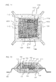
FIG. 1 is a plan view of a semiconductor device according to a first embodiment. The semiconductor device has a leadframe 100, a first semiconductor chip 200, and a second semiconductor chip 300. The leadframe 100 has a die pad 101, first marks 112, and second marks 122. The die pad 101 allows thereon mounting of the first semiconductor chip 200. The first marks 112 indicate a mounting region 110 for the first semiconductor chip 200, and the second marks 122 indicate a mounting region 120 for the second semiconductor chip 300. The first marks 112 are different from the second marks 122 in at least size and geometry. In this illustrated example, the first mark 112 and the second mark 122 have nearly circular geometry, but have different sizes. More specifically, the first marks 112 are larger than the second marks 122.
Note that first recesses, projections or holes may be adoptable in place of the first marks 112, and second recesses, projections or holes may be adoptable in place of the second marks 122.
The first recesses 112 and the second recesses 122 typically have diameters of equal to or larger than 0.05 mm and equal to or smaller than 0.3 mm, and typically have depths of equal to or deeper than 0.01 mm and equal to or shallower than 0.05 mm. All of the first recesses 112 and the second recesses 122 are positioned outside the mounting region 110 for the first semiconductor chip 200, and outside the mounting region 120 for the second semiconductor chip 300.
In this illustrated example, the second semiconductor chip 300 is smaller than the first semiconductor chip 200, and is mounted over the first semiconductor chip 200. The mounting region 120 for the second semiconductor chip 300 is positioned inside the mounting region 110 for the first semiconductor chip 200.
The die pad 101 has a nearly square or rectangular geometry, and has a plurality of first recesses 112 and a plurality of second recesses 122. The mounting region 110 for the first semiconductor chip 200 is defined by the lines connecting every adjacent first recesses 112. The mounting region 120 for the second semiconductor chip 300 is defined by the lines connecting every correspondent second recesses 122 faced each other through the mounting region 110 for the first semiconductor chip 200 in between.
In this illustrated example, the mounting region 110 for the first semiconductor chip 200 defined by the first recesses 112 is larger than the first semiconductor chip 200, and indicates an allowable range of the mounting position of the first semiconductor chip 200. Also the mounting region 120 for the second semiconductor chip 300 defined by the second recesses 122 is larger than the second semiconductor chip 300, and indicates an allowable range of the mounting position of the second semiconductor chip 300. Alternatively, the mounting region 110 for the first semiconductor chip 200 may have the same geometry with the first semiconductor chip 200, so as to make the mounting region 110 indicate the mounting position of the first semiconductor chip 200 on the design basis. Still alternatively, the mounting region 120 for the second semiconductor chip 300 may have the same geometry with the second semiconductor chip 300, so as to make the mounting region 120 indicate the mounting position of the second semiconductor chip 300 on the design basis.
FIG. 2 is a sectional view of the semiconductor device illustrated in FIG. 1. In addition to the configuration illustrated in FIG. 1, the semiconductor device illustrated in the drawing has wires 410, 420 and an encapsulation resin 500. The wires 410 connect pads (not illustrated) of the first semiconductor chip 200 and inner leads (not illustrated) of the leadframe 100, and the wires 420 connect pads (not illustrated) of the second semiconductor chip 300 and inner leads (not illustrated) of the leadframe 100.
The encapsulation resin 500 encapsulates the surface of the die pad of the leadframe 100, the inner leads, the first semiconductor chip 200, the second semiconductor chip 300, and the wires 410, 420. In this illustrated example, the lower surface of the die pad 101 of the leadframe 100 exposes to the bottom surface of the encapsulation resin 500.
FIG. 3 is a sectional view illustrating a modified example of the semiconductor device illustrated in FIG. 2. The semiconductor device illustrated in the drawing is configured similarly to the semiconductor device illustrated in FIG. 2, except that also the lower surface of the die pad 101 is encapsulated in the encapsulation resin 500.
Paragraphs below will explain a method of manufacturing the semiconductor device illustrated in FIGS. 1 to 3. First, the leadframe 100 is obtained, and the first recesses 112 and the second recesses 122 are formed thereto. The first recesses 112 and the second recesses 122 are formed as impressions, typically by pressing a jig downward against the die pad 101 of the leadframe 100.
For an alternative case where projections are adopted in place of the first recesses 112 and the second recesses 122, the projections are formed as impressions, typically by pressing a jig upward against the die pad 101 of the leadframe 100. For a still alternative case where holes are adopted in place of the first recesses 112 and the second recesses 122, the holes are formed typically by using a punch.
Next, the first semiconductor chip 200 is mounted on the die pad 101, and the second semiconductor chip 300 is further mounted on the first semiconductor chip 200. An apparatus for mounting the first semiconductor chip 200 used herein recognizes the first recesses 112 by image processing or by using a sensor, and determines a mounting position of the first semiconductor chip 200. On the other hand, an apparatus for mounting the second semiconductor chip 300 recognizes the second recesses 122 by image processing or by using a sensor, and determines a mounting position of the second semiconductor chip 300.
Next, the pads of the first semiconductor chip 200 are connected to the inner leads of the leadframe 100 using the wires 410. Furthermore, the pads of the second semiconductor chip 300 are connected to the inner leads of the leadframe 100 using the wires 420.
Next, the mounting position of the first semiconductor chip 200 is visually inspected based on a relative position between the first recesses 112 and the first semiconductor chip 200, and the mounting position of the second semiconductor chip 300 is visually inspected based on a relative position between the second recesses 122 and the second semiconductor chip 300. More specifically, the mounting position of the first semiconductor chip 200 is judged as being correct, if the first semiconductor chip 200 does not fall beyond the mounting region 110 defined by the recesses 112. On the other hand, the mounting position of the second semiconductor chip 300 is judged as being correct, if the second semiconductor chip 300 does not fall beyond the mounting region 120 defined by the second recesses 122.
If both mounting positions of the first semiconductor chip 200 and the second semiconductor chip 300 are judged as being correct, the encapsulation resin 500 is formed using a mold, so as to encapsulate the die pad 101 and the inner leads of the leadframe 100, the first semiconductor chip 200, the second semiconductor chip 300, and the wires 410, 420. For the case where the semiconductor device is configured as illustrated in FIG. 3, and the holes are formed in place of the first recesses 112 and the second recesses 122, the encapsulation resin 500 intrudes also in the holes, to thereby improve adhesiveness between the encapsulation resin 500 and the leadframe 100.
Next, operations and effect of this embodiment will be explained. The first recesses 112 indicate the mounting region 110 for the first semiconductor chip 200, and the second recesses 122 indicate the mounting region 120 for the second semiconductor chip 300. The first recesses 112 and the second recesses 122 are different from each other in at least either one of size and geometry. Accordingly, the mounting region 110 for the first semiconductor chip 200 and the mounting region 120 for the second semiconductor chip 300 may readily be recognized, in whatever cases of adopting the image processing, the sensor and visual inspection.
More specifically, the apparatus for mounting the semiconductor chip onto the die pad 101 may readily recognize the mounting region 110 for the first semiconductor chip 200, and the mounting region 120 for the second semiconductor chip 300. Also for the case where the mounting position of each of the first semiconductor chip 200 and the second semiconductor chip 300 is visually inspected, each of the mounting region 110 for the first semiconductor chip 200 and the mounting region 120 for the second semiconductor chip 300 may readily be recognized.
The first recesses 112 and the second recesses 122 may be formed simply by pressing a jig against the die pad 101, needing only a low cost for forming the first recesses 112 and the second recesses 122.
The first recesses 112 and the second recesses 122, provided so as not to extend through the die pad 101, are contributive to suppress decrease in the strength of the die pad 101, and also to suppress the flatness of the die pad 101 from degrading.
Alternatively by using only a single type of leadframe 100, a first semiconductor device having only the first semiconductor chip 200 mounted on the die pad 101, and a second semiconductor device having only the second semiconductor chip 300 mounted on the die pad 101 may be manufactured. In this way, only a single type of leadframe 100 may be used commonly for the first and second semiconductor devices having different chip sizes. The above-described effects may be obtained also in this case.
FIG. 4 is a plan view of a semiconductor device according to a second embodiment, and corresponds to FIG. 1 in the first embodiment. The semiconductor device is configured similarly to the semiconductor device explained in the first embodiment, except for the planar geometry of the die pad 101. The die pad 101 of this embodiment has a nearly octagonal geometry.
For the case where the die pad 101 has a non-simple geometry just like this embodiment, it may not be easy to recognize the distance from the edges of the die pad 101 to the first semiconductor chip 200 and to the second semiconductor chip 300. It may therefore be difficult to inspect the mounting position of the first semiconductor chip 200 and the second semiconductor chip 300, based on the distance from the edges of the die pad 101. In contrast in this embodiment, the mounting region 110 for the first semiconductor chip 200 is defined by the first recesses 112, and the mounting region 120 for the second semiconductor chip 300 is defined by the second recesses 122. The mounting positions of the first semiconductor chip 200 and the second semiconductor chip 300 may readily be inspected.
FIG. 5 is a plan view of a semiconductor device according to a third embodiment, and corresponds to FIG. 1 in the first embodiment. The semiconductor device is configured similarly to the semiconductor device explained in the first embodiment, except that the first recesses 112 and the second recesses 122 have different geometries.
The effects similar to those in the first embodiment may be obtained also in this embodiment. Since the first recesses 112 and the second recesses 122 may be formed to have the same size, both of the first recesses 112 and the second recesses 122 may more readily be confirmed by visual inspection.
FIG. 6 is a plan view of a semiconductor device according to a fourth embodiment, and corresponds to FIG. 1 in the first embodiment. The semiconductor device is configured similarly to the semiconductor device explained in the first embodiment, except that a third semiconductor chip 600 is mounted over the second semiconductor chip 300, and that a plurality of third recesses 132 are formed to the die pad 101. The third recesses 132 may be formed in the same step of forming the first recesses 112 and the second recesses 122.
The third semiconductor chip 600 is smaller than the second semiconductor chip 300. The third recesses 132 are different from both of the first recesses 112 and the second recesses 122, in at least either one of size and geometry. The plurality of third recesses 132 indicate a mounting region 130 for the third semiconductor chip 600. The mounting region 130 is defined by the lines connecting the correspondent third recesses 132 faced each other through the mounting region 120 for the second semiconductor chip 300 in between.
Effects similar to those in the first embodiment may be obtained also in this embodiment. Also mounting and inspection of the mounting position of the third semiconductor chip 600 may be carried out similarly to the mounting and inspection of the mounting positions of the first semiconductor chip 200 and the second semiconductor chip 300.
FIG. 7 is a plan view of a semiconductor device according to a fifth embodiment, and corresponds to FIG. 6 in the fourth embodiment. The semiconductor device is configured similarly to as described in the fourth embodiment, except that both of the second semiconductor chip 300 and the third semiconductor chip 600 are mounted over the first semiconductor chip 200.
Effects similar to those in the fourth embodiment may be obtained also in this embodiment.
FIG. 8 is a plan view of a semiconductor device according to a sixth embodiment, and corresponds to FIG. 1 in the first embodiment. The semiconductor device is configured similarly to as described in the first embodiment, except that the second semiconductor chip 300 is mounted on the die pad 101 of the leadframe 100, rather than on the first semiconductor chip 200.
Effects similar to those in the first embodiment may be obtained also in this embodiment.
FIG. 9 is a plan view of a semiconductor device according to a seventh embodiment, and FIG. 10 is a schematic sectional view of the semiconductor device illustrated in FIG. 9. The semiconductor device is configured similarly to as described in the first embodiment, except for the aspects below. First, the first semiconductor chip 200 is mounted on a first surface of the die pad 101 of the leadframe 100, and the second semiconductor chip 300 is mounted on a second surface, which is the surface opposite to the first surface, of the die pad 101. The first recesses 112 are formed to the first surface of the die pad 101, and the second recesses 122 are formed to the second surface of the die pad 101.
According to this embodiment, the first recesses 112 formed to the first surface of the die pad 101 are different from the second recesses 122 formed to the second surface of the die pad 101, in at least either one of size and geometry. Accordingly, the surface to be mounted thereon with the first semiconductor chip 200, and the surface to be mounted thereon with the second semiconductor chip 300 may readily be understood in a respective manner. Therefore, the mounting surface for the first semiconductor chip 200 and the mounting surface for the second semiconductor chip 300 may be less likely to be mistaken.
FIG. 11 is a plan view of a semiconductor device according to an eighth embodiment, and FIG. 12 is a schematic sectional view of the semiconductor device illustrated in FIG. 11. The semiconductor device is configured similarly to as described in the fourth embodiment, except for the aspects below. First, the first surface of the die pad 101 of the leadframe 100 has the first semiconductor chip 200 and the second semiconductor chip 300 mounted thereon. The second surface of the die pad 101, which is the surface opposite to the first surface, has the third semiconductor chip 600 mounted thereon. The first surface of the die pad 101 has also the first recesses 112 and the second recesses 122 formed thereto, and the second surface of the die pad 101 has the third recess 132 formed thereto.
As illustrated in FIG. 12, the second semiconductor chip 300 in this embodiment is directly connected to the leadframe 100 through a part of the wires 420, and connected to the first semiconductor chip 200 through the residual wires 420. The third semiconductor chip 600 is directly connected to the leadframe 100 through wires 430.
Effects similar to those in the fourth embodiment may be obtained also in this embodiment. The first recesses 112 and the second recesses 122 formed to the first surface of the die pad 101 are different from the third recesses 132 formed to the second surface of the die pad 101, in at least either one of size and geometry. Accordingly, the surface to be mounted thereon with the first semiconductor chip 200 and the second semiconductor chip 300, and the surface to be mounted thereon with the third semiconductor chip 600 may readily be recognized in a respective manner. Therefore, the mounting surface for the first semiconductor chip 200 and the second semiconductor chip 300, and the mounting surface for the second semiconductor chip 300 may be less likely to be mistaken.
In the seventh embodiment, the first recesses 112 and the second recesses 122 may have the same geometry and the same size. In the eighth embodiment, the third recesses 132 may have the same size and the same geometry with the first recesses 112 or the second recesses 122.
The embodiments of the present invention have been explained referring to the attached drawings, merely as examples of the present invention, while allowing adoption of various configurations other than those described in the above.
It is apparent that the present invention is not limited to the above embodiments, but may be modified and changed without departing from the scope and spirit of the invention.

Claims (4)

What is claimed is:
1. A method of manufacturing a semiconductor device comprising:
mounting at least one of a first semiconductor chip and a second semiconductor chip over a die pad of a leadframe; and
inspecting a mounting position of at least one of said first semiconductor chip and said second semiconductor chip;
wherein said leadframe comprises:
a first mark formed to said die pad, for indicating a first mounting region for said first semiconductor chip; and
a second mark formed to said die pad, for indicating a second mounting region for said second semiconductor chip;
said first mark is different from said second mark, in at least either one of size and geometry,
wherein, in said inspecting a mounting position of at least one of said first semiconductor chip and said second semiconductor chip, a mounting position of said first semiconductor chip is inspected when said first semiconductor chip is mounted, based on a relative position of said first semiconductor chip with respect to said first mark, and a mounting position of said second semiconductor chip is inspected when said second semiconductor chip is mounted, based on a relative position of said second semiconductor chip with respect to said second mark.
2. The leadframe as claimed in claim 1,
wherein said first mark is one of a recess, a projection and a hole, and said second mark is one of a recess, a projection and a hole.
3. The method of manufacturing a semiconductor device as claimed in claim 1,
wherein said first semiconductor chip is larger than said second semiconductor chip,
and
in said mounting at least one of said first semiconductor chip and said second semiconductor chip over said die pad, said first semiconductor chip is mounted over said die pad, and said second semiconductor chip is mounted over said first semiconductor chip.
4. The method of manufacturing a semiconductor device as claimed in claim 3,
wherein said leadframe has a plurality of said first marks, and a plurality of said second marks,
wherein said first mounting region for said first semiconductor chip is defined by the lines connecting every adjacent first recesses, projections or holes, and
said second mounting region for said second semiconductor chip is defined by the lines connecting every correspondent second recesses, projections or holes faced each other through said mounting region for said first semiconductor chip in between.
US14/268,847 2008-08-01 2014-05-02 Leadframe, semiconductor device, and method of manufacturing the same Active US9029195B2 (en)

Priority Applications (1)

Application Number Priority Date Filing Date Title
US14/268,847 US9029195B2 (en) 2008-08-01 2014-05-02 Leadframe, semiconductor device, and method of manufacturing the same

Applications Claiming Priority (6)

Application Number Priority Date Filing Date Title
JP2008-199186 2008-08-01
JP2008199186A JP5097639B2 (en) 2008-08-01 2008-08-01 Lead frame and semiconductor device
US12/458,951 US8164203B2 (en) 2008-08-01 2009-07-28 Leadframe, semiconductor device, and method of manufacturing the same
US13/427,777 US8487454B2 (en) 2008-08-01 2012-03-22 Leadframe, semiconductor device, and method of manufacturing the same
US13/933,498 US8786112B2 (en) 2008-08-01 2013-07-02 Leadframe, semiconductor device, and method of manufacturing the same
US14/268,847 US9029195B2 (en) 2008-08-01 2014-05-02 Leadframe, semiconductor device, and method of manufacturing the same

Related Parent Applications (1)

Application Number Title Priority Date Filing Date
US13/933,498 Division US8786112B2 (en) 2008-08-01 2013-07-02 Leadframe, semiconductor device, and method of manufacturing the same

Publications (2)

Publication Number Publication Date
US20140242734A1 US20140242734A1 (en) 2014-08-28
US9029195B2 true US9029195B2 (en) 2015-05-12

Family

ID=41607484

Family Applications (4)

Application Number Title Priority Date Filing Date
US12/458,951 Active 2029-11-23 US8164203B2 (en) 2008-08-01 2009-07-28 Leadframe, semiconductor device, and method of manufacturing the same
US13/427,777 Active US8487454B2 (en) 2008-08-01 2012-03-22 Leadframe, semiconductor device, and method of manufacturing the same
US13/933,498 Active US8786112B2 (en) 2008-08-01 2013-07-02 Leadframe, semiconductor device, and method of manufacturing the same
US14/268,847 Active US9029195B2 (en) 2008-08-01 2014-05-02 Leadframe, semiconductor device, and method of manufacturing the same

Family Applications Before (3)

Application Number Title Priority Date Filing Date
US12/458,951 Active 2029-11-23 US8164203B2 (en) 2008-08-01 2009-07-28 Leadframe, semiconductor device, and method of manufacturing the same
US13/427,777 Active US8487454B2 (en) 2008-08-01 2012-03-22 Leadframe, semiconductor device, and method of manufacturing the same
US13/933,498 Active US8786112B2 (en) 2008-08-01 2013-07-02 Leadframe, semiconductor device, and method of manufacturing the same

Country Status (2)

Country Link
US (4) US8164203B2 (en)
JP (1) JP5097639B2 (en)

Families Citing this family (6)

* Cited by examiner, † Cited by third party
Publication number Priority date Publication date Assignee Title
DE60335538D1 (en) * 2002-03-12 2011-02-10 Hamamatsu Photonics Kk METHOD FOR CUTTING A PROCESSED OBJECT
JP5097639B2 (en) * 2008-08-01 2012-12-12 ルネサスエレクトロニクス株式会社 Lead frame and semiconductor device
JP5820979B2 (en) * 2008-12-26 2015-11-24 パナソニックIpマネジメント株式会社 Solid-state imaging device
US8205397B2 (en) * 2009-08-25 2012-06-26 Hot Edge, Inc. Roof edge cable raceway and method of forming same
DE102019118174B3 (en) * 2019-07-04 2020-11-26 Infineon Technologies Ag PROCESSING OF ONE OR MORE CARRIER BODIES AND ELECTRONIC COMPONENTS THROUGH MULTIPLE ALIGNMENT
CN112563147B (en) * 2020-12-07 2023-05-12 英特尔产品(成都)有限公司 Method, device and system for detecting bag removal of semiconductor chip product

Citations (16)

* Cited by examiner, † Cited by third party
Publication number Priority date Publication date Assignee Title
JPS5684360A (en) 1979-12-06 1981-07-09 Nippon Steel Chemical Co Manufacture of lightweight material
JPS5818948A (en) 1981-07-27 1983-02-03 Toshiba Corp Lead frame
JPS6185159A (en) 1984-10-03 1986-04-30 Hoshino Bussan Kk Method and apparatus for continuous exchange preparation of plural kinds of noodles
JPS62163962A (en) 1986-01-14 1987-07-20 Nec Corp Ultrasonic microscope
US6081029A (en) 1998-03-12 2000-06-27 Matsushita Electronics Corporation Resin encapsulated semiconductor device having a reduced thickness and improved reliability
US20030092216A1 (en) 2001-11-09 2003-05-15 Advanced Semiconductor Engineering, Inc. Method of manufacturing a semiconductor package with a lead frame having a support structure
US6740961B1 (en) 2000-06-09 2004-05-25 National Semiconductor Corporation Lead frame design for chip scale package
US6891254B2 (en) 2001-12-28 2005-05-10 Seiko Epson Corporation Semiconductor device with protrusions
US6900524B1 (en) 1997-06-27 2005-05-31 Matsushita Electric Industrial Co., Ltd. Resin molded semiconductor device on a lead frame and method of manufacturing the same
US6906424B2 (en) * 2002-08-02 2005-06-14 Micron Technology, Inc. Semiconductor package and method producing same
JP2007134659A (en) 2005-11-14 2007-05-31 Sharp Corp Lead frame, semiconductor device, semiconductor device manufacturing method, and electronic apparatus
US7262491B2 (en) 2005-09-06 2007-08-28 Advanced Interconnect Technologies Limited Die pad for semiconductor packages and methods of making and using same
JP2008124116A (en) 2006-11-09 2008-05-29 Denso Corp Semiconductor device
US20090085179A1 (en) * 2007-09-28 2009-04-02 Renesas Technology Corp. Semiconductor device
US7554181B2 (en) * 2004-03-31 2009-06-30 Renesas Technology Corp. Semiconductor device with non-overlapping chip mounting sections
US8178955B2 (en) 2002-04-01 2012-05-15 Panasonic Corporation Semiconductor device

Family Cites Families (2)

* Cited by examiner, † Cited by third party
Publication number Priority date Publication date Assignee Title
JPS6185159U (en) * 1984-11-08 1986-06-04
JP5097639B2 (en) * 2008-08-01 2012-12-12 ルネサスエレクトロニクス株式会社 Lead frame and semiconductor device

Patent Citations (16)

* Cited by examiner, † Cited by third party
Publication number Priority date Publication date Assignee Title
JPS5684360A (en) 1979-12-06 1981-07-09 Nippon Steel Chemical Co Manufacture of lightweight material
JPS5818948A (en) 1981-07-27 1983-02-03 Toshiba Corp Lead frame
JPS6185159A (en) 1984-10-03 1986-04-30 Hoshino Bussan Kk Method and apparatus for continuous exchange preparation of plural kinds of noodles
JPS62163962A (en) 1986-01-14 1987-07-20 Nec Corp Ultrasonic microscope
US6900524B1 (en) 1997-06-27 2005-05-31 Matsushita Electric Industrial Co., Ltd. Resin molded semiconductor device on a lead frame and method of manufacturing the same
US6081029A (en) 1998-03-12 2000-06-27 Matsushita Electronics Corporation Resin encapsulated semiconductor device having a reduced thickness and improved reliability
US6740961B1 (en) 2000-06-09 2004-05-25 National Semiconductor Corporation Lead frame design for chip scale package
US20030092216A1 (en) 2001-11-09 2003-05-15 Advanced Semiconductor Engineering, Inc. Method of manufacturing a semiconductor package with a lead frame having a support structure
US6891254B2 (en) 2001-12-28 2005-05-10 Seiko Epson Corporation Semiconductor device with protrusions
US8178955B2 (en) 2002-04-01 2012-05-15 Panasonic Corporation Semiconductor device
US6906424B2 (en) * 2002-08-02 2005-06-14 Micron Technology, Inc. Semiconductor package and method producing same
US7554181B2 (en) * 2004-03-31 2009-06-30 Renesas Technology Corp. Semiconductor device with non-overlapping chip mounting sections
US7262491B2 (en) 2005-09-06 2007-08-28 Advanced Interconnect Technologies Limited Die pad for semiconductor packages and methods of making and using same
JP2007134659A (en) 2005-11-14 2007-05-31 Sharp Corp Lead frame, semiconductor device, semiconductor device manufacturing method, and electronic apparatus
JP2008124116A (en) 2006-11-09 2008-05-29 Denso Corp Semiconductor device
US20090085179A1 (en) * 2007-09-28 2009-04-02 Renesas Technology Corp. Semiconductor device

Non-Patent Citations (4)

* Cited by examiner, † Cited by third party
Title
Japanese Office Action dated Jun. 19, 2012 with English Translation.
Japanese Office Action, dated Sep. 3, 2013 with English translation.
U.S. Notice of Allowance dated Feb. 18, 2014 in U.S. Appl. No. 13/933,498.
U.S. Office Action dated Sep. 24, 2013, in U.S. Appl. No. 13/933,498.

Also Published As

Publication number Publication date
US20120175760A1 (en) 2012-07-12
JP5097639B2 (en) 2012-12-12
US8164203B2 (en) 2012-04-24
US20140242734A1 (en) 2014-08-28
US20130285227A1 (en) 2013-10-31
US8487454B2 (en) 2013-07-16
US8786112B2 (en) 2014-07-22
JP2010040618A (en) 2010-02-18
US20100025839A1 (en) 2010-02-04

Similar Documents

Publication Publication Date Title
US9029195B2 (en) Leadframe, semiconductor device, and method of manufacturing the same
US7642133B2 (en) Method of making a semiconductor package and method of making a semiconductor device
JP2005322921A (en) Flip-chip semiconductor package for testing bumps and method of fabricating same
US9620388B2 (en) Integrated circuit package fabrication with die attach paddle having middle channels
US9966329B2 (en) Method for manufacturing semiconductor device
TWI445139B (en) Chip package structure, chip package mold chase and chip package process
KR100614797B1 (en) Chuck table for manufacturing semiconductor
JP5566433B2 (en) Manufacturing method of semiconductor device
US9202778B2 (en) Integrated circuit package with die attach paddle having at least one recessed portion
US7432588B2 (en) Semiconductor device and method of fabricating the same
JP2007294568A (en) Semiconductor device
JP2008071927A (en) Manufacturing method of semiconductor device, and semiconductor device
JP5701579B2 (en) Manufacturing method of semiconductor device
JP2016201447A (en) Molded package
US6867507B2 (en) Lead frame
US20060197199A1 (en) Leadframe, coining tool, and method
JP4948035B2 (en) Manufacturing method of resin-encapsulated semiconductor device
US11600557B2 (en) Packaged device having selective lead pullback for dimple depth control
US20100109157A1 (en) Chip structure and chip package structure
JP4835449B2 (en) Semiconductor device
KR100362499B1 (en) Expressive method for badness of a semiconductor package and thereby the semiconductor package
JP2007294637A (en) Method for manufacturing semiconductor device
JPH06291241A (en) Semiconductor device
JP2009176987A (en) Semiconductor apparatus and method of manufacturing the same
JPH073142U (en) IC socket

Legal Events

Date Code Title Description
STCF Information on status: patent grant

Free format text: PATENTED CASE

AS Assignment

Owner name: RENESAS ELECTRONICS CORPORATION, JAPAN

Free format text: CHANGE OF ADDRESS;ASSIGNOR:RENESAS ELECTRONICS CORPORATION;REEL/FRAME:044928/0001

Effective date: 20150806

MAFP Maintenance fee payment

Free format text: PAYMENT OF MAINTENANCE FEE, 4TH YEAR, LARGE ENTITY (ORIGINAL EVENT CODE: M1551); ENTITY STATUS OF PATENT OWNER: LARGE ENTITY

Year of fee payment: 4

MAFP Maintenance fee payment

Free format text: PAYMENT OF MAINTENANCE FEE, 8TH YEAR, LARGE ENTITY (ORIGINAL EVENT CODE: M1552); ENTITY STATUS OF PATENT OWNER: LARGE ENTITY

Year of fee payment: 8