US9024982B2 - Driving method of image display device - Google Patents
Driving method of image display device Download PDFInfo
- Publication number
- US9024982B2 US9024982B2 US14/455,203 US201414455203A US9024982B2 US 9024982 B2 US9024982 B2 US 9024982B2 US 201414455203 A US201414455203 A US 201414455203A US 9024982 B2 US9024982 B2 US 9024982B2
- Authority
- US
- United States
- Prior art keywords
- pixel
- sub
- input signal
- signal
- value
- Prior art date
- Legal status (The legal status is an assumption and is not a legal conclusion. Google has not performed a legal analysis and makes no representation as to the accuracy of the status listed.)
- Active
Links
Images
Classifications
-
- G—PHYSICS
- G09—EDUCATION; CRYPTOGRAPHY; DISPLAY; ADVERTISING; SEALS
- G09G—ARRANGEMENTS OR CIRCUITS FOR CONTROL OF INDICATING DEVICES USING STATIC MEANS TO PRESENT VARIABLE INFORMATION
- G09G3/00—Control arrangements or circuits, of interest only in connection with visual indicators other than cathode-ray tubes
- G09G3/20—Control arrangements or circuits, of interest only in connection with visual indicators other than cathode-ray tubes for presentation of an assembly of a number of characters, e.g. a page, by composing the assembly by combination of individual elements arranged in a matrix no fixed position being assigned to or needed to be assigned to the individual characters or partial characters
- G09G3/34—Control arrangements or circuits, of interest only in connection with visual indicators other than cathode-ray tubes for presentation of an assembly of a number of characters, e.g. a page, by composing the assembly by combination of individual elements arranged in a matrix no fixed position being assigned to or needed to be assigned to the individual characters or partial characters by control of light from an independent source
- G09G3/3406—Control of illumination source
- G09G3/3413—Details of control of colour illumination sources
-
- G—PHYSICS
- G09—EDUCATION; CRYPTOGRAPHY; DISPLAY; ADVERTISING; SEALS
- G09G—ARRANGEMENTS OR CIRCUITS FOR CONTROL OF INDICATING DEVICES USING STATIC MEANS TO PRESENT VARIABLE INFORMATION
- G09G3/00—Control arrangements or circuits, of interest only in connection with visual indicators other than cathode-ray tubes
- G09G3/20—Control arrangements or circuits, of interest only in connection with visual indicators other than cathode-ray tubes for presentation of an assembly of a number of characters, e.g. a page, by composing the assembly by combination of individual elements arranged in a matrix no fixed position being assigned to or needed to be assigned to the individual characters or partial characters
- G09G3/34—Control arrangements or circuits, of interest only in connection with visual indicators other than cathode-ray tubes for presentation of an assembly of a number of characters, e.g. a page, by composing the assembly by combination of individual elements arranged in a matrix no fixed position being assigned to or needed to be assigned to the individual characters or partial characters by control of light from an independent source
- G09G3/36—Control arrangements or circuits, of interest only in connection with visual indicators other than cathode-ray tubes for presentation of an assembly of a number of characters, e.g. a page, by composing the assembly by combination of individual elements arranged in a matrix no fixed position being assigned to or needed to be assigned to the individual characters or partial characters by control of light from an independent source using liquid crystals
- G09G3/3611—Control of matrices with row and column drivers
- G09G3/3648—Control of matrices with row and column drivers using an active matrix
-
- G—PHYSICS
- G09—EDUCATION; CRYPTOGRAPHY; DISPLAY; ADVERTISING; SEALS
- G09G—ARRANGEMENTS OR CIRCUITS FOR CONTROL OF INDICATING DEVICES USING STATIC MEANS TO PRESENT VARIABLE INFORMATION
- G09G3/00—Control arrangements or circuits, of interest only in connection with visual indicators other than cathode-ray tubes
- G09G3/20—Control arrangements or circuits, of interest only in connection with visual indicators other than cathode-ray tubes for presentation of an assembly of a number of characters, e.g. a page, by composing the assembly by combination of individual elements arranged in a matrix no fixed position being assigned to or needed to be assigned to the individual characters or partial characters
- G09G3/34—Control arrangements or circuits, of interest only in connection with visual indicators other than cathode-ray tubes for presentation of an assembly of a number of characters, e.g. a page, by composing the assembly by combination of individual elements arranged in a matrix no fixed position being assigned to or needed to be assigned to the individual characters or partial characters by control of light from an independent source
- G09G3/3406—Control of illumination source
- G09G3/342—Control of illumination source using several illumination sources separately controlled corresponding to different display panel areas, e.g. along one dimension such as lines
- G09G3/3426—Control of illumination source using several illumination sources separately controlled corresponding to different display panel areas, e.g. along one dimension such as lines the different display panel areas being distributed in two dimensions, e.g. matrix
-
- G—PHYSICS
- G09—EDUCATION; CRYPTOGRAPHY; DISPLAY; ADVERTISING; SEALS
- G09G—ARRANGEMENTS OR CIRCUITS FOR CONTROL OF INDICATING DEVICES USING STATIC MEANS TO PRESENT VARIABLE INFORMATION
- G09G2300/00—Aspects of the constitution of display devices
- G09G2300/04—Structural and physical details of display devices
- G09G2300/0439—Pixel structures
- G09G2300/0452—Details of colour pixel setup, e.g. pixel composed of a red, a blue and two green components
-
- G—PHYSICS
- G09—EDUCATION; CRYPTOGRAPHY; DISPLAY; ADVERTISING; SEALS
- G09G—ARRANGEMENTS OR CIRCUITS FOR CONTROL OF INDICATING DEVICES USING STATIC MEANS TO PRESENT VARIABLE INFORMATION
- G09G2320/00—Control of display operating conditions
- G09G2320/06—Adjustment of display parameters
- G09G2320/0626—Adjustment of display parameters for control of overall brightness
- G09G2320/0646—Modulation of illumination source brightness and image signal correlated to each other
-
- G—PHYSICS
- G09—EDUCATION; CRYPTOGRAPHY; DISPLAY; ADVERTISING; SEALS
- G09G—ARRANGEMENTS OR CIRCUITS FOR CONTROL OF INDICATING DEVICES USING STATIC MEANS TO PRESENT VARIABLE INFORMATION
- G09G2340/00—Aspects of display data processing
- G09G2340/06—Colour space transformation
-
- G—PHYSICS
- G09—EDUCATION; CRYPTOGRAPHY; DISPLAY; ADVERTISING; SEALS
- G09G—ARRANGEMENTS OR CIRCUITS FOR CONTROL OF INDICATING DEVICES USING STATIC MEANS TO PRESENT VARIABLE INFORMATION
- G09G2360/00—Aspects of the architecture of display systems
- G09G2360/14—Detecting light within display terminals, e.g. using a single or a plurality of photosensors
- G09G2360/145—Detecting light within display terminals, e.g. using a single or a plurality of photosensors the light originating from the display screen
Definitions
- the present disclosure relates to a driving method of an image display device.
- a color image display device disclosed in Japanese Patent No. 3167026 includes a unit configured to generate three types of color signals by the three primary additive color method from an input signal, and a unit configured to generate an auxiliary signal obtained by adding each of the color signals of these three hues with the same ratio, and to supply the display signals in total of four types of the auxiliary signal, and the three types of color signals obtained by subtracting the auxiliary signal from the signals of the three hues to a display device.
- the red display sub-pixel, green display sub-pixel, and blue display sub-pixel are driven, and the white display sub-pixel is driven by the auxiliary signal.
- a liquid crystal display device configured of a first pixel made up of a red display sub-pixel, a green display sub-pixel, and a blue display sub-pixel, and a second pixel made up of a red display sub-pixel, a green display sub-pixel, and a white display sub-pixel, a first pixel and a second pixel are alternately arrayed in a first direction, and also arrayed in a second direction, or alternatively, there has been disclosed a liquid crystal display device wherein a first pixel and a second pixel are alternately arrayed in the first direction, and also in a second direction a first pixel is adjacently arrayed, and moreover, a second pixel is adjacently arrayed.
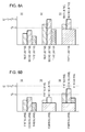
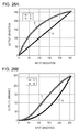
- a method for handling such a phenomenon include a method for changing a tone curve ( ⁇ curve). For example, if description will be made with a tone curve as a reference, in the event that output gradation as to input gradation when there is no influence of external light has a relation such as a straight line “A” shown in FIG. 26A , output gradation as to input gradation when there is influence of external light is changed to a relation shown in a curve “B” in FIG. 26A .
- change of output gradation (output luminance) as to input gradation is performed as to each of a red display sub-pixel, a green display sub-pixel, and a blue display sub-pixel making up each pixel based on change of a tone curve ( ⁇ curve), and accordingly, a ratio of (luminance of a red display sub-pixel:luminance of a green display sub-pixel:luminance of a blue display sub-pixel) before change, and a ratio of (luminance of a red display sub-pixel:luminance of a green display sub-pixel:luminance of a blue display sub-pixel) after change usually differ.
- a problem occurs such that an image after change has a light color and loses contrast feeling as compared to an image before change.
- An image display device driving method for providing the above-described image display device driving method is a driving method of an image display device including an image display panel configured of pixels being arrayed in a two-dimensional matrix shape, each of which is made up of a first sub-pixel for displaying a first primary color, a second sub-pixel for displaying a second primary color, a third sub-pixel for displaying a third primary color, and a fourth sub-pixel for displaying a fourth color, and a signal processing unit, the method causing the signal processing unit to obtain a first sub-pixel output signal based on at least a first sub-pixel input signal and an extension coefficient ⁇ 0 to output to the first sub-pixel, to obtain a second sub-pixel output signal based on at least a second sub-pixel input signal and the extension coefficient ⁇ 0 to output to the second sub-pixel, to obtain a third sub-pixel output signal
- An image display device driving method for providing the above-described image display device driving method is a driving method of an image display device including an image display panel configured of pixels being arrayed in a two-dimensional matrix shape in a first direction and a second direction, each of which is made up of a first sub-pixel for displaying a first primary color, a second sub-pixel for displaying a second primary color, and a third sub-pixel for displaying a third primary color, a pixel group being made up of at least a first pixel and a second pixel arrayed in the first direction, and a fourth sub-pixel for displaying a fourth color being disposed between a first pixel and a second pixel at each pixel group, and a signal processing unit, the method causing the signal processing unit with regard to a first pixel to obtain a first sub-pixel output signal based on at least a
- An image display device driving method for providing the above-described image display device driving method is a driving method of an image display device including an image display panel configured of pixel groups being arrayed in a two-dimensional matrix shape in total of P ⁇ Q pixel groups of P pixel groups in a first direction, and Q pixel groups in a second direction, each pixel group of which is made up of a first pixel and a second pixel in the first direction, where the first pixel is made up of a first sub-pixel for displaying a first primary color, a second sub-pixel for displaying a second primary color, and a third sub-pixel for displaying a third primary color, and the second pixel is made up of a first sub-pixel for displaying a first primary color, a second sub-pixel for displaying a second primary color, and a fourth sub-pixel for displaying a fourth color, and a signal
- An image display device driving method for providing the above-described image display device driving method is a driving method of an image display device including an image display panel configured of pixels being arrayed in a two-dimensional matrix shape in total of P 0 ⁇ Q 0 pixels of P 0 pixels in a first direction, and Q 0 pixels in a second direction, each pixel of which is made up of a first sub-pixel for displaying a fist primary color, a second sub-pixel for displaying a second primary color, a third sub-pixel for displaying a third primary color, and a fourth sub-pixel for displaying a fourth color, and a signal processing unit, the method causing the signal processing unit to obtain a first sub-pixel output signal based on at least a first sub-pixel input signal and an extension coefficient ⁇ 0 to output to the first sub-pixel, to obtain a second sub-pixel output signal based
- An image display device driving method for providing the above-described image display device driving method is a driving method of an image display device including an image display panel configured of pixel groups being arrayed in a two-dimensional matrix shape in total of P ⁇ Q pixel groups of P pixel groups in a first direction, and Q pixel groups in a second direction, each of which is made up of a first pixel and a second pixel in the first direction, where the first pixel is made up of a first sub-pixel for displaying a first primary color, a second sub-pixel for displaying a second primary color, and a third sub-pixel for displaying a third primary color, and the second pixel is made up of a first sub-pixel for displaying a first primary color, a second sub-pixel for displaying a second primary color, and a fourth sub-pixel for displaying a fourth color, and a signal
- a fourth sub-pixel control first signal obtained from a first sub-pixel input signal, a second sub-pixel input signal, and a third sub-pixel input signal as to an adjacent pixel adjacent to the (p, q)'th second pixel in the second direction, and an extension coefficient ⁇ 0 to output the fourth sub-pixel of the (p, q)'th second pixel, and to obtain a third sub-pixel output signal based on at least the third sub-pixel input signal as to the (p, q)'th second pixel, and the third sub-pixel input signal as to the (p, q)'th first pixel, and the extension coefficient ⁇ 0 to output the third sub-pixel of the (p, q)'th first pixel.
- the image display device driving methods include: obtaining the maximum value V max of luminosity at the signal processing unit with saturation S in the HSV color space enlarged by adding a fourth color, as a variable; obtaining a reference extension coefficient ⁇ 0-std at the signal processing unit based on the maximum value V max ; and determining an extension coefficient ⁇ 0 at each pixel from the reference extension coefficient ⁇ 0-std , an input signal correction coefficient based on the sub-pixel input signal values at each pixel, and an external light intensity correction coefficient based on external light intensity.
- the saturation S can take a value from 0 to 1
- the luminosity V(S) can take a value from 0 to (2 n ⁇ 1)
- n is the number of display gradation bits
- H of “HSV color space” means Hue indicating the type of color
- S means Saturation (Saturation, chromaticity) indicating vividness of a color
- V means luminosity (Brightness Value, Lightness Value) indicating brightness of a color. This can be applied to the following description.
- the image display device driving methods according to the sixth mode through the tenth mode of the present disclosure include: obtaining a reference extension coefficient ⁇ 0-std from the following expression, assuming that the luminance of a group of a first sub-pixel, a second sub-pixel and a third sub-pixel making up a pixel (the sixth mode and ninth mode in the present disclosure) or a pixel group (the seventh mode, eighth mode, and tenth mode in the present disclosure) is BN 1-3 at the time of a signal having a value equivalent to the maximum signal value of a first sub-pixel output signal being input to a first sub-pixel, a signal having a value equivalent to the maximum signal value of a second sub-pixel output signal being input to a second sub-pixel, and a signal having a value equivalent to the maximum signal value of a third sub-pixel output signal being input to a third sub-pixel, and assuming that the luminance of the fourth sub-pixel is BN 4 at the time of a signal having a value equivalent to the maximum
- ⁇ 0-std (BN 4 /BN 1-3 )+1; and determining an extension coefficient ⁇ 0 at each pixel from the reference extension coefficient ⁇ 0-std , an input signal correction coefficient based on the sub-pixel input signal values at each pixel, and an external light intensity correction coefficient based on external light intensity.
- these modes can be taken as a mode with the reference extension coefficient ⁇ 0-std as a function of (BN 4 /BN 1-3 ).
- the image display device driving methods according to the eleventh mode through the fifteenth mode of the present disclosure include: determining a reference extension coefficient ⁇ 0-std to be less than a predetermined value ⁇ ′ 0-std (e.g., specifically 1.3 or less) when a color defined with (R, G, B) is displayed with a pixel, hue H and saturation S in the HSV color space are defined with the following expressions, and a ratio of pixels satisfying the following ranges as to all the pixels exceeds a predetermined value ⁇ ′ 0 (e.g., specifically 2%) 40 ⁇ H ⁇ 65 0.5 ⁇ S ⁇ 1.0; and determining an extension coefficient ⁇ 0 at each pixel from the reference extension coefficient ⁇ 0-std , an input signal correction coefficient based on the sub-pixel input signal values at each pixel, and an external light intensity correction coefficient based on external light intensity.
- the lower limit value of the reference extension coefficient ⁇ 0-std is 1.0. This can be applied to the following description.
- the image display device driving methods include: determining a reference extension coefficient ⁇ 0-std to be less than a predetermined value ⁇ 0-std (e.g., specifically 1.3 or less) when a color defined with (R, G, B) is displayed with a pixel, and a ratio of pixels of which the (R, G, B) satisfy the following expressions as to all the pixels exceeds a predetermined value ⁇ ′ 0 (e.g., specifically 2%); and determining an extension coefficient ⁇ 0 at each pixel from the reference extension coefficient ⁇ 0-std , an input signal correction coefficient based on the sub-pixel input signal values at each pixel, and an external light intensity correction coefficient based on external light intensity.
- a predetermined value ⁇ 0-std e.g., specifically 1.3 or less
- ⁇ ′ 0 e.g., specifically 2%
- the image display device driving methods include: determining a reference extension coefficient ⁇ 0-std to be less than a predetermined value (e.g., specifically 1.3 or less) when a ratio of pixels which display yellow as to all the pixels exceeds a predetermined value ⁇ ′ 0 (e.g., specifically 2%); and determining an extension coefficient ⁇ 0 at each pixel from the reference extension coefficient ⁇ 0-std , an input signal correction coefficient based on the sub-pixel input signal values at each pixel, and an external light intensity correction coefficient based on external light intensity.
- a predetermined value e.g., specifically 1.3 or less
- ⁇ ′ 0 e.g., specifically 2%
- the image display device driving methods determine an extension coefficient ⁇ 0 at each pixel from the reference extension coefficient ⁇ 0-std , an input signal correction coefficient based on the sub-pixel input signal values at each pixel, and an external light intensity correction coefficient based on external light intensity. Accordingly, a problem in that visibility of an image displayed on an image display device under a bright environment where external light irradiates the image display device, can be solved, and moreover, optimization of luminance at each pixel can be realized.
- the color space (HSV color space) is enlarged by adding the fourth color, and a sub-pixel output signal can be obtained based on at least a sub-pixel input signal and the reference extension coefficient ⁇ 0-std and the extension coefficient ⁇ 0 .
- an output signal value is extended based on the reference extension coefficient ⁇ 0-std and the extension coefficient ⁇ 0 , and accordingly, an arrangement may not be made wherein, like the related art, through the luminance of the white display sub-pixel increases, the luminance of the red display sub-pixel, green display sub-pixel, and blue display sub-pixel does not increase.
- the luminance of the white display sub-pixel is increased, but also the luminance of the red display sub-pixel, green display sub-pixel, and blue display sub-pixel is increased. Moreover, a ratio of (luminance of a red display sub-pixel:luminance of a green display sub-pixel:luminance of a blue display sub-pixel) is not changed in principle. Therefore, change in a color can be prevented, and occurrence of a problem such as dullness of a color can be prevented in a sure manner. Note that when the luminance of the white display sub-pixel increases, but the luminance of the red display sub-pixel, green display sub-pixel, and blue display sub-pixel does not increase, dullness of a color occurs. Such a phenomenon is referred to as simultaneous contrast. In particular, occurrence of such phenomenon is marked regarding yellow where visibility is high.
- the maximum value V max of luminosity with the saturation S serving as a variable is obtained, and further, the reference extension coefficient ⁇ 0-std is determined so that a ratio of pixels wherein the value of extended luminosity obtained from product between the luminosity V(S) of each pixel and the reference extension coefficient ⁇ 0-std exceeds the maximum value V max , as to all the pixels is less than a predetermined value ( ⁇ 0 ).
- optimization of an output signal as to each sub-pixel can be realized, and occurrence of a phenomenon with marked conspicuous gradation deterioration which causes an unnatural image can be prevented, and on the other hand, increase in luminance can be realized in a sure manner, and reduction of power consumption of the entire image display device assembly in which the image display device has been built can be realized.
- the reference extension coefficient ⁇ 0-std is set to a predetermined value ⁇ ′ 0-std or less (e.g., specifically 1.3 or less).
- the reference extension coefficient ⁇ 0-std is set to a predetermined value ⁇ 0-std or less (e.g., specifically 1.3 or less).
- the reference extension coefficient ⁇ 0-std is set to a predetermined value or less (e.g., specifically 1.3 or less).
- the image display device driving methods according to the first mode, sixth mode, eleventh mode, sixteenth mode, and twenty-first mode of the present disclosure can realize increase in the luminance of a display image, and are the most appropriate to image display such as still images, advertising media, standby screen for cellar phones, and so forth, for example.
- the image display device driving methods according to the first mode, sixth mode, eleventh mode, sixteenth mode, and twenty-first mode of the present disclosure are applied to an image display device assembly driving method, whereby the luminance of a planar light source device can be reduced based on the reference extension coefficient ⁇ 0-std , and accordingly, reduction in the power consumption of the planar light source device can be realized.
- the image display device driving methods according to the second mode, third mode, seventh mode, eighth mode, twelfth mode, thirteenth mode, seventeenth mode, eighteenth mode, twenty-second mode, and twenty-third mode of the present disclosure cause the signal processing unit to obtain the fourth sub-pixel output signal from the first sub-pixel input signal, second sub-pixel input signal, and third sub-pixel input signal as to the first pixel and the second pixel of each pixel group, and output this. That is to say, the fourth sub-pixel output signal is obtained based on the input signals as to the adjacent first and second pixels, and accordingly, optimization of the output signal as to the fourth sub-pixel is realized.
- a single fourth sub-pixel is disposed as to the pixel group made up of at least the first pixel and the second pixel, and accordingly, reduction in the area of an opening region at a sub-pixel can be suppressed. As a result thereof, increase in luminance can be realized in a sure manner, and improvement in display quality can be realized. Also, the consumption power of backlight can be reduced.
- the fourth sub-pixel output signal as to the (p, q)'th pixel is obtained based on a sub-pixel input signal as to the (p, q)'th pixel, and a sub-pixel input signal as to an adjacent pixel adjacent to the (p, q)'th pixel in the second direction. That is to say, a fourth sub-pixel output signal as to a certain pixel is obtained based on an input signal as to an adjacent pixel adjacent to this certain pixel, and accordingly, optimization of an output signal as to the fourth sub-pixel is realized. Also, according to the fourth sub-pixel being provided, increase in luminance can be realized in a sure manner, and also improvement in display quality can be realized.
- the fourth sub-pixel output signal as to the (p, q)'th second pixel is obtained based on a sub-pixel input signal as to the (p, q)'th second pixel, and a sub-pixel input signal as to an adjacent pixel adjacent to this second pixel in the second direction.
- the fourth sub-pixel output signal as to the second pixel making up a certain pixel group is obtained based on not only an input signal as to the second pixel making up this certain pixel group but also an input signal as to an adjacent pixel adjacent to this second pixel, and accordingly, optimization of an output signal as to the fourth sub-pixel is realized.
- a single fourth sub-pixel is disposed as to a pixel group made up of the first pixel and the second pixel, and accordingly, reduction in the area of an opening region in a sub-pixel can be suppressed. As a result thereof, increase in luminance can be realized in a sure manner, and also improvement in display quality can be realized.
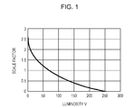
- FIG. 1 is a schematic graph of an input signal correction coefficient represented with a function with luminosity at each pixel serving as a parameter;
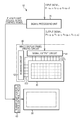
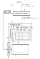
- FIG. 2 is a conceptual diagram of an image display device according a first embodiment
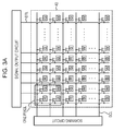
- FIGS. 3A and 3B are conceptual diagrams of an image display panel and an image display panel driving circuit of the image display device according to the first embodiment
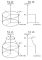
- FIGS. 4A and 4B are a conceptual diagram of common columnar HSV color space, and a diagram schematically illustrating a relation between saturation and luminosity respectively
- FIGS. 4C and 4D are a conceptual diagram of columnar HSV color space enlarged in the first embodiment, and a diagram schematically illustrating a relation between saturation and luminosity respectively;
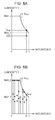
- FIGS. 5A and 5B are each diagrams schematically illustrating a relation between saturation and luminosity in columnar HSV color space enlarged by adding a fourth color (white) in the first embodiment;
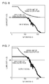
- FIG. 6 is a diagram illustrating a relation between HSV color space according to the related art before adding the fourth color (white) in the first embodiment, HSV color space enlarged by adding a fourth color (white), and the saturation and luminosity of an input signal;
- FIG. 7 is a diagram illustrating a relation between HSV color space according to the related art before adding the fourth color (white) in the first embodiment, HSV color space enlarged by adding a fourth color (white), and the saturation and luminosity of an output signal (subjected to extension processing);
- FIGS. 8A and 8B are diagrams schematically illustrating an input signal value and an output signal value for describing difference between an image display device driving method according to the first embodiment, extension processing of an image display device assembly driving method, and a processing method disclosed in Japanese Patent No. 3805150;
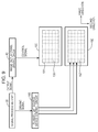
- FIG. 9 is a conceptual diagram of an image display panel and a planar light source device making up an image display device assembly according to a second embodiment
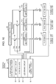
- FIG. 10 is a circuit diagram of a planar light source device control circuit of a planar light source device making up the image display device assembly according to the second embodiment
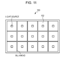
- FIG. 11 is a diagram schematically illustrating layout and array states of a planar light source unit and so forth of the planar light source device making up the image display device assembly according to the second embodiment;
- FIGS. 12A and 12B are conceptual diagrams for describing a state increasing/decreasing the light source luminance of the planar light source unit under the control of the planar light source device driving circuit so as to obtain display luminance second specified value by the planar light source unit at the time of assuming that a control signal equivalent to an intra-display region unit signal maximum value is supplied to a sub-pixel;
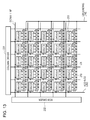
- FIG. 13 is an equivalent circuit diagram of an image display device according to a third embodiment
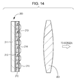
- FIG. 14 is a conceptual diagram of an image display panel making up the image display device according to the third embodiment.
- FIG. 15 is a diagram schematically illustrating the layout of each pixel and a pixel group of an image display panel according to a fourth embodiment
- FIG. 16 is a diagram schematically illustrating the layout of each pixel and a pixel group of an image display panel according to a fifth embodiment
- FIG. 17 is a diagram schematically illustrating the layout of each pixel and a pixel group of an image display panel according to a sixth embodiment
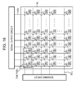
- FIG. 18 is a conceptual diagram of an image display panel and an image display panel driving circuit of the image display device according to the fourth embodiment.
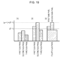
- FIG. 19 is a diagram schematically illustrating an input signal value and an output signal value at extension processing of an image display device driving method and an image display device assembly driving method according the fourth embodiment
- FIG. 20 is a diagram schematically illustrating the layout of each pixel and a pixel group of an image display panel according to a seventh embodiment, an eight embodiment, or a tenth embodiment;
- FIG. 21 is a diagram schematically illustrating another layout example of each pixel and a pixel group of an image display panel according to a seventh embodiment, an eight embodiment, or a tenth embodiment;
- FIG. 22 is, with regard to an eighth embodiment, a conceptual diagram for describing a modification of an array of a first sub-pixel, a second sub-pixel, a third sub-pixel, and a fourth sub-pixel of a first pixel and a second pixel making up a pixel group;
- FIG. 23 is a diagram schematically illustrating a layout example of each pixel of an image display device according to a ninth embodiment
- FIG. 24 is a diagram schematically illustrating another layout example of each pixel and a pixel group of an image display device according to a tenth embodiment
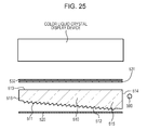
- FIG. 25 is a conceptual diagram of an edge light type (side light type) planar light source device.
- FIGS. 26A and 26B are a graph schematically illustrating output gradation as to input gradation depending on whether or not there is influence of external light, and a graph schematically illustrating output luminance as to input gradation depending on whether or not there is influence of external light, respectively.
- the image display device assembly according to the image display device assembly driving methods according to the first mode through the twenty-fifth mode for providing a desirable image display device driving method is the above-described image display devices according to the first mode through the twenty-fifth mode of the present disclosure, and an image display device assembly including a planar light source device which irradiates the image display devices from behind.
- the image display device driving methods according to the first mode through the twenty-fifth mode of the present disclosure can be applied to the image display device assembly driving methods according to the first mode through the twenty-fifth mode.
- the image display device driving methods according to the first mode through the twenty-fifth mode and the image display device assembly driving methods according to the first mode through the twenty-fifth mode including the above-described preferred mode will collectively referred to simply as “driving method of the present disclosure”.
- the input signal correction coefficient k IS can be represented with a function with sub-pixel input signal values at each pixel serving as parameters, and specifically, a function with luminosity V(S) at each pixel serving as a parameter, for example. More specifically, for example, there can be exemplified a function wherein the value of the input signal correction coefficient k IS is the minimum value (e.g., “0”) when the value of the luminosity V(S) is the maximum value, and the value of the input signal correction coefficient k IS is the maximum value when the value of the luminosity V(S) is the minimum value, and an upward protruding function wherein the value of the input signal correction coefficient k IS is the minimum value (e.g., “0”) when the value of the luminosity V(S) is the maximum value and the minimum value.
- the minimum value e.g., “0”
- the external light intensity correction coefficient k OL is a constant depending on external light intensity, and for example, the value of the external light intensity correction coefficient k OL is increased under an environment where the sunlight in the summer is strong, and the value of the external light intensity correction coefficient k OL is decreased under an environment where the sunlight is weak or an indoor environment.
- the value of the external light intensity correction coefficient k OL may be selected by the user of the image display device using a changeover switch or the like provided to the image display device, for example, or an arrangement may be made wherein external light intensity is measured by an optical sensor provided to the image display device, and the image display device selects the value of the external light intensity correction coefficient k OL based on the result thereof.
- a function of the input signal correction coefficient k IS is suitably selected, whereby increase in the luminance of a pixel from intermediate gradation to low gradation can be realized for example, and on the other hand, gradation deterioration at pixels of high gradation can be suppressed, and also a signal exceeding the maximum luminance can be prevented from being output to a pixel of high gradation, or alternatively, for example, change (increase or decrease) of the contrast of a pixel having intermediate gradation can be obtained, and additionally, the value of the external light intensity correction coefficient k OL is suitably selected, and accordingly, correction according to external light intensity can be performed, and visibility of an image displayed on the image display device can be prevented in a surer manner from deteriorating due to environment light being changed.
- the reference extension coefficient ⁇ 0-std is obtained based on the maximum value V max , but specifically, of the values of V max /V(S) obtained at multiple pixels, the reference extension coefficient ⁇ 0-std can be obtained based on at least one value.
- the V max means the maximum value of the V(S) obtained at multiple pixels, as described above. More specifically, this may be taken as a mode wherein of the values of V max /V(S) [ ⁇ (S)] obtained at multiple pixels, the minimum value ( ⁇ min ) is taken as the reference extension coefficient ⁇ 0-std .
- the reference extension coefficient ⁇ 0-std may be taken as the reference extension coefficient ⁇ 0-std .
- the reference extension coefficient ⁇ 0-std may be obtained based on one value (e.g., the minimum value ⁇ min ), or an arrangement may be made wherein multiple values ⁇ (S) are obtained in order from the minimum value, a mean value ( ⁇ ave ) of these values is taken as the reference extension coefficient ⁇ 0-std , or further, a mean value of multiple values of (1 ⁇ 0.4) L ave may be taken as the reference extension coefficient ⁇ 0-std .
- the reference extension coefficient ⁇ 0-std may be determined such that a ratio of pixels wherein the value of extended luminosity obtained from product between luminosity V(S) and the reference extension coefficient ⁇ 0-std exceeds the maximum value V max , as to all of the pixels is a predetermined value ( ⁇ 0 ) or less.
- 0.003 through 0.05 may be given as the predetermined value ⁇ 0 .
- the reference extension coefficient ⁇ 0-std is determined such that a ratio of pixels wherein the value of extended luminosity obtained from product between the luminosity V(S) and the reference extension coefficient ⁇ 0-std exceeds the maximum value V max becomes equal to or greater than 0.3% and also equal to or less than 5% as to all of the pixels.
- the signal processing unit may be configured to output a first sub-pixel output signal for determining the display gradation of a first sub-pixel of which the signal value is x 1-(p, q) , to output a second sub-pixel output signal for determining the display gradation of a second sub-pixel of which the signal value is x 2-(p, q) , to output a third sub-pixel output signal for
- the driving method according to the second mode and so forth of the present disclosure, the third mode and so forth of the present disclosure, or the fifth mode and so forth of the present disclosure including the above-described preferred mode, with regard to a first pixel making up the (p, q)'th pixel group (where 1 ⁇ p ⁇ P, 1 ⁇ q ⁇ Q), a first sub-pixel input signal of which the signal value is x 1-(p, q)-1 , a second sub-pixel input signal of which the signal value is x 2-(p, q)-1 , and a third sub-pixel input signal of which the signal value is x 3-(p, q)-1 are input to the signal processing unit, and with regard to a second pixel making up the (p, q)'th pixel group, a first sub-pixel input signal of which the signal value is x 1-(p, q)-2 , a second sub-pixel input signal of which the signal value is x 2-(p, q)-2 , and a third sub-pixel input signal
- a first sub-pixel input signal of which the signal value is x 1-(p′, q) , a second sub-pixel input signal of which the signal value is x 2-(p′, q) , and a third sub-pixel input signal of which the signal value is x 3-(p′, q) may be arranged to be input to the signal processing unit.
- a first sub-pixel input signal of which the signal value is x 1-(p, q′) , a second sub-pixel input signal of which the signal value is x 2-(p, q′) , and a third sub-pixel input signal of which the signal value is x 3-(p, q) may be arranged to be input to the signal processing unit.
- Max (p, q) , Min (p, q) , Max (p, q) , Min (p, q)-1 , Max (p, q)-2 , Min (p, q)-2 , Max (p′, q)-1 , Min (p′, q)-1 , Max (p, q′) , and Min (p, q′) are defined as follows.
- Max (p, q) the maximum value of three sub-pixel input signal values of a first sub-pixel input signal value x 1-(p, q) , a second sub-pixel input signal value x 2-(p, q) , and a third sub-pixel input signal value x 3-(p, q) as to the (p, q)'th pixel
- Min (p, q) the minimum value of three sub-pixel input signal values of the first sub-pixel input signal value x 1-(p, q) , the second sub-pixel input signal value x 2-(p, q) , and the third sub-pixel input signal value x 3-(p, q) as to the (p, q)'th pixel
- Max (p, q)-1 the maximum value of three sub-pixel input signal values of a first sub-pixel input signal value x 1-(p, q)-1 , a second sub-pixel input signal value x 2-(p, q)-1 , and a third sub-pixel input signal value x 3-(p, q)-1 as to the (p, q)'th first pixel
- Min (p, q)-1 the minimum value of three sub-pixel input signal values of the first sub-pixel input signal value x 1-(p, q)-1 , the second sub-pixel input signal value x 2-(p, q)-1 , and the third sub-pixel input signal value x 3-(p, q)-1 as to the (p, q)'th first pixel
- Max (p, q)-2 the maximum value of three sub-pixel input signal values of a first sub-pixel input signal value x 1-(p, q)-2 , a second sub-pixel input signal value x 2-(p, q)-2 , and a third sub-pixel input signal value x 3-(p, q)-2 as to the (p, q)'th second pixel
- Min (p, q)-2 the minimum value of three sub-pixel input signal values of the first sub-pixel input signal value x 1-(p, q)-2 , the second sub-pixel input signal value x 2-(p, q)-2 , and the third sub-pixel input signal value x 3-(p, q)-2 as to the (p, q)'th second pixel
- Max (p′, q)-1 the maximum value of three sub-pixel input signal values of a first sub-pixel input signal value x 1-(p′, q) , a second sub-pixel input signal value x 2-(p′q) , and a third sub-pixel input signal value x 3-(p′q) as to an adjacent pixel adjacent to the (p, q)'th second pixel in the first direction
- Min (p′,q)-1 the minimum value of three sub-pixel input signal values of the first sub-pixel input signal value x 1-(p′, q) , the second sub-pixel input signal value x 2-(p′,q) , and the third sub-pixel input signal value x 3-(p′,q) as to an adjacent pixel adjacent to the (p, q)'th second pixel in the first direction
- Max (p, q′) the maximum value of three sub-pixel input signal values of a first sub-pixel input signal value x 1-(p, q′) , a second sub-pixel input signal value x 2-(p, q′) , and a third sub-pixel input signal value x 3-(p, q′) as to an adjacent pixel adjacent to the (p, q)'th second pixel in the second direction
- Min (p, q′) the minimum value of three sub-pixel input signal values of the first sub-pixel input signal value x 1-(p, q′) , the second sub-pixel input signal value x 2-(p, q′) , and the third sub-pixel input signal value x 3-(p, q′) as to an adjacent pixel adjacent to the (p, q)'th second pixel in the second direction
- the value of the fourth sub-pixel output signal may be arranged to be obtained based on at least the value of Min and the extension coefficient ⁇ 0 .
- a fourth sub-pixel output signal value X 4-(p, q) can be obtained from the following Expressions, for example, where c 11 , c 12 , c 13 , c 14 , c 15 , and c 16 are constants. Note that, it is desirable to determine what kind of value or expression is used as the value of the X 4-(p, q) as appropriate by experimentally manufacturing an image display device or image display device assembly, and performing image evaluation by an image observer.
- an arrangement may be made wherein a first sub-pixel output signal is obtained based on at least a first sub-pixel input signal and the extension coefficient ⁇ 0 , a second sub-pixel output signal is obtained based on at least a second sub-pixel input signal and the extension coefficient ⁇ 0 , and a third sub-pixel output signal is obtained based on at least a third sub-pixel input signal and the extension coefficient ⁇ 0 .
- the signal processing unit can obtain a first sub-pixel output signal value X 1-(p, q) , a second sub-pixel output signal value X 2-(p, q) , and a third sub-pixel output signal value X 3-(p, q) as to the (p, q)'th pixel (or a set of a first sub-pixel, second sub-pixel, and third sub-pixel) from the following expressions.
- X 1-(p,q) ⁇ 0 ⁇ x 1-(p,q) ⁇ SG 2-(p,q) (1-D)
- X 2-(p,q) ⁇ 0 ⁇ x 2-(p,q) ⁇ SG 2-(p,q) (1-E)
- X 3-(p,q) ⁇ 0 ⁇ x 3-(p,q) ⁇ SG 2-(p,q) (1-F)
- the constant ⁇ is a value is a value specific to an image display device or image display device assembly, and is unambiguously determined by the image display device or image display device assembly.
- the constant ⁇ can also be applied to the following description in the same way.
- a first sub-pixel output signal is obtained based on at least a first sub-pixel input signal and the extension coefficient ⁇ 0 , but a first sub-pixel output signal (signal value X 1-(p, q)-1 ) is obtained based on at least a first sub-pixel input signal (signal value x 1-(p, q)-1 ) and the extension coefficient ⁇ 0 , and a fourth sub-pixel control first signal (signal value SG 1-(p, q) ), a second sub-pixel output signal is obtained based on at least a second sub-pixel input signal and the extension coefficient ⁇ 0 , but a second sub-pixel output signal (signal value x 2-(p, q)-1 ) is obtained based on at least a second sub-pixel input signal (signal value x 2-(p, q)-1 ) and the extension coefficient ⁇ 0
- the first sub-pixel output signal value X 1-(p, q)-1 is obtained based on at least the first sub-pixel input signal value x 1-(p, q)-1 and the extension coefficient ⁇ 0
- the fourth sub-pixel control first signal value SG 1-(p, q) but the first sub-pixel output signal value X 1-(p, q)-1 may be obtained based on [ x 1-(p,q)-1 , ⁇ 0 ,SG 1-(p,q) ], or may be obtained based on [ x 1-(p,q)-1 ,x 1-(p,q)-2 , ⁇ 0 ,SG 1-(p,q) ]
- the second sub-pixel output signal value x 2-(p, q)-1 is obtained based on at least the second sub-pixel input signal value x 2-(p, q)-1 and the extension coefficient ⁇ 0
- the output signal values X 1-(p, q)-1 , X 2-(p, q)-1 , X 3-(p, q)-1 , X 1-(p, q)-2 , X 2-(p, q)-2 , and X 3-(p, q)-2 can be obtained at the signal processing unit from the following expressions.
- X 1-(p,q)-1 ⁇ 0 ⁇ x 1-(p,q)-1 ⁇ SG 1-(p,q) (2-A)
- X 2-(p,q)-1 ⁇ 0 ⁇ x 2-(p,q)-1 ⁇ SG 1-(p,q) (2-B)
- X 3-(p,q)-1 ⁇ 0 ⁇ x 3-(p,q)-1 ⁇ SG 1-(p,q) (2-C)
- X 1-(p,q)-2 ⁇ 0 ⁇ x 1-(p,q)-2 ⁇ SG 2-(p,q) (2-D)
- X 2-(p,q)-2 ⁇ 0 ⁇ x 2-(p,q)-2 ⁇ SG 2-(p,q) (2-E)
- X 3-(p,q)-2 ⁇ 0 ⁇ x 3-(p,q)-2 ⁇ SG 2-(p,q) (2-F)
- a first sub-pixel output signal is obtained based on at least a first sub-pixel input signal and the extension coefficient ⁇ 0 , but a first sub-pixel output signal (signal value X 1-(p, q)-2 ) is obtained based on at least a first sub-pixel input signal value x 1-(p, q)-2 and the extension coefficient ⁇ 0 , and a fourth sub-pixel control second signal (signal value SG 2-(p, q) ), a second sub-pixel output signal is obtained based on at least a second sub-pixel input signal and the extension coefficient ⁇ 0 , but a second sub-pixel output signal (signal value X 2-(p, q)-2 ) is obtained based on at least a second sub-pixel input signal value x 2-(p, q)-2 and the extension coefficient ⁇ 0 , and
- the output signal values x 1-(p, q)-2 , X 2-(p, q)-2 , X 1-(p, q)-1 , and X 2-(p, q)-1 can be obtained at the signal processing unit from the following expressions.
- X 1-(p,q)-2 ⁇ 0 ⁇ x 1-(p,q)-2 ⁇ SG 2-(p,q) (3-A)
- X 2-(p,q)-2 ⁇ 0 ⁇ x 2-(p,q)-2 ⁇ SG 2-(p,q) (3-B)
- X 1-(p,q)-1 ⁇ 0 ⁇ x 1-(p,q)-1 ⁇ SG 1-(p,q) (3-C)
- X 2-(p,q)-1 ⁇ 0 ⁇ x 2-(p,q)-1 ⁇ SG 1-(p,q) (3-D) or
- X 1-(p,q)-1 ⁇ 0 ⁇ x 1-(p,q)-1 ⁇ SG 3-(p,q) (3-E)
- X 2-(p,q)-1 ⁇ 0 ⁇ x 2-(p,q)-1 ⁇ SG 3-(p,q) (3-F)
- the third sub-pixel output signal (third sub-pixel output signal value X 3-(p, q)-1 ) of the first pixel can be obtained from the following expressions when assuming that C 31 and C 32 are taken as constants, for example.
- the fourth sub-pixel control first signal (signal value SG 1-(p, q) ) and the fourth sub-pixel control second signal (signal value SG 2-(p, q) ) can specifically be obtained from the following expressions, for example, where c 21 , c 22 , c 23 , c 24 , c 25 , and c 26 are constants. Note that, it is desirable to determine what kind of value or expression is used as the values of the X 4-(p, q) and X 4-(p, q)-2 as appropriate by experimentally manufacturing an image display device or image display device assembly, and performing image evaluation by an image observer, for example.
- the Max (p, q)-1 and Min (p, q)-1 in the above-described expressions should be read as Max (p′, q)-1 and Min (p′, q)-1 .
- the Max (p, q)-1 and Min (p, q)-1 in the above-described expressions should be read as Max (p, q′) and Min (p, q′) .
- control signal value (third sub-pixel control signal value) SG 3-(p, q) can be obtained by replacing “SG 1-(p, q) ” in the left-hand side in the Expression (2-1-1), Expression (2-2-1), Expression (2-3-1), Expression (2-4-1), Expression (2-5-1), and Expression (2-6-1) with “SG 3-(p, q) ”.
- One of the above-described expressions may be selected depending on the value of SG 4-(p, q) , one of the above-described expressions may be selected depending on the value of SG 2-(p, q) , or one of the above-described expressions may be selected depending on the values of SG 4-(p, q) and SG 2-(p, q) .
- X 4-(p, q) and X 4-(p, q) may be obtained by fixing to one of the above expressions, or with each pixel group, X 4-(p, q) and X 4-(p, q)-2 may be obtained by selecting one of the above expressions.
- the adjacent pixel is adjacent to the (p, q)'th second pixel in the first direction, but the adjacent pixel may be arranged to be adjacent to the (p, q)'th first pixel, or alternatively, the adjacent pixel may be arranged to be adjacent to the (p+1, q)'th first pixel.
- an arrangement may be made wherein, in the second direction, a first pixel and a first pixel are adjacently disposed, and a second pixel and a second pixel are adjacently disposed, or alternatively, an arrangement may be made wherein, in the second direction, a first pixel and a second pixel are adjacently disposed.
- a first pixel is, in the first direction, made up of a first sub-pixel for displaying a first primary color, a second sub-pixel for displaying a second primary color, and a third sub-pixel for displaying a third primary color being sequentially arrayed
- a second pixel is, in the first direction, made up of a first sub-pixel for displaying a first primary color, a second sub-pixel for displaying a second primary color, and a fourth sub-pixel for displaying a fourth color being sequentially arrayed. That is to say, it is desirable to dispose a fourth sub-pixel a downstream edge portion of a pixel group in the first direction.
- the layout is not restricted to these, and for example, such as an arrangement wherein a first pixel is, in the first direction, made up of a first sub-pixel for displaying a first primary color, a third sub-pixel for displaying a third primary color, and a second sub-pixel for displaying a second primary color being sequentially arrayed, and a second pixel is, in the first direction, made up of a first sub-pixel for displaying a first primary color, a fourth sub-pixel for displaying a fourth color, and a second sub-pixel for displaying a second primary color being sequentially arrayed, it is desirable to select one of 36 combinations of 6 ⁇ 6 in total.
- six combinations can be given as array combinations of (first sub-pixel, second sub-pixel, and third sub-pixel) in a first pixel, and six combinations can be given as array combinations of (first sub-pixel, second sub-pixel, and fourth sub-pixel) in a second pixel.
- the shape of a sub-pixel is a rectangle, but it is desirable to dispose a sub-pixel such that the longer side of this rectangle is parallel to the second direction, and the shorter side is parallel to the first direction.
- the (p, q ⁇ 1)'th pixel may be given as an adjacent pixel adjacent to the (p, q)'th pixel or as an adjacent pixel adjacent to the (p, q)'th second pixel, or alternatively, the (p, q+1)'th pixel may be given, or alternatively, the (p, q ⁇ 1)'th pixel and the (p, q+1)'th pixel may be given.
- the reference extension coefficient ⁇ 0-std may be arranged to be determined for each one image display frame. Also, with the driving methods according to the first mode and so forth through the fifth mode and so forth of the present disclosure, an arrangement may be made depending on circumstances wherein the luminance of a light source for illuminating an image display device (e.g., planar light source device) is reduced based on the reference extension coefficient ⁇ 0-std .
- a light source for illuminating an image display device e.g., planar light source device
- the shape of a sub-pixel is a rectangle, but it is desirable to dispose a sub-pixel such that the longer side of this rectangle is parallel to the second direction, and the shorter side is parallel to the first direction.
- the shape is not restricted to this.
- a mode for employing multiple pixels or pixel groups from which the saturation S and luminosity V(S) are to be obtained there may be available a mode for employing all of the pixels or pixel groups, or alternatively, a mode for employing (1/N) of all the pixels or pixel groups.
- N is a natural number of two or more.
- factorial of 2 such as 2, 4, 8, 16, and so on can be exemplified. If the former mode is employed, image quality can suitably be held at a maximum without change in image quality. On the other hand, if the latter mode is employed, improvement in processing speed, and simplification of the circuits of the signal processing unit can be realized.
- a mode may be employed wherein the fourth color is white.
- the fourth color is not restricted to this, and additionally, yellow, cyan, or magenta may be taken as the fourth color, for example.
- an arrangement may be made wherein a first color filter disposed between a first sub-pixel and the image observer for passing a first primary color, a second color filter disposed between a second sub-pixel and the image observer for passing a second primary color, and a third color filter disposed between a third sub-pixel and the image observer for passing a third primary color are further provided.
- Examples of a light source making up the planar light source device include a light emitting device, and specifically, a light emitting diode (LED).
- a light emitting device made up of a light emitting diode has small occupied volume, which is suitable for disposing multiple light emitting devices.
- Examples of a light emitting diode serving as a light emitting device include a white light emitting diode (e.g., a light emitting diode which emits white by combining an ultraviolet or blue light emitting diode and a light emitting particle).
- examples of a light emitting particle include a red-emitting fluorescent particle, a green-emitting fluorescent particle, and a blue-emitting fluorescent particle.
- materials making up a red-emitting fluorescent particle include Y 2 O 3 :Eu, YVO 4 :Eu, Y(P, V)O 4 :Eu, 3.5MgO.0.5MgF 2 .Ge 2 :Mn, CaSiO 3 :Pb,Mn, Mg 6 AsO 11 :Mn, (Sr, Mg) 3 (PO 4 ) 3 :Sn, La 2 O 2 S:Eu, Y 2 O 2 S:Eu, (ME:Eu)S [where “ME” means at least one kind of atom selected from a group made up of Ca, Sr, and Ba, this can be applied to the following description], (M:Sm) x (Si, Al) 12 (O, N) 16 [where “M” means at least one kind of atom selected from a
- Examples of materials making up a green-emitting fluorescent particle include LaPO 4 :Ce,Tb, BaMgAl 11 O 17 :Eu,Mn, Zn 2 SiO 4 :Mn, MgAl 11 O 19 :Ce,Tb, Y 2 SiO 5 :Ce,Tb, MgAl 11 O 19 :CE,Tb,Mn, and further include (ME:Eu)Ga 2 S 4 , (M:RE) x (Si, Al) 12 (O, N) 16 [where “RE” means Tb and Yb], (M:Tb) x (Si, Al) 12 (O, N) 16 , and (M:Yb) x (Si, Al) 12 (O, N) 16 .
- examples of materials making up a blue-emitting fluorescent particle include BaMgAl 10 O 17 :Eu, BaMg 2 Al 16 O 17 :Eu, Sr 2 P 2 O 7 :Eu, Sr 5 (PO 4 ) 3 Cl:Eu, (Sr, Ca, Ba, Mg) 5 (PO 4 ) 3 Cl:Eu, CaWO 4 , and CaWO 4 :Pb.
- light emitting particles are not restricted to fluorescent particles, and for example, with an indirect transition type silicon material, there can be given a light emitting particle to which a quantum well structure such as a two-dimensional quantum well structure, a one-dimensional quantum well structure (quantum wire), a zero-dimensional quantum well structure (quantum dots) or the like has been applied which localizes a carrier wave function for effectively converting carriers into light using quantum effects like a direct transition type, it is familiar that RE atom added to a semiconductor material emits light keenly by interior transition, and a light emitting particle to which such a technique has been applied can also be given.
- a quantum well structure such as a two-dimensional quantum well structure, a one-dimensional quantum well structure (quantum wire), a zero-dimensional quantum well structure (quantum dots) or the like
- a light source making up the planar light source device can be configured of a combination of a red-emitting device (e.g., lighting emitting diode) for emitting red (e.g., main emission wavelength of 640 nm), a green-emitting device (e.g., GaN lighting emitting diode) for emitting red (e.g., main emission wavelength of 530 nm), and a blue-emitting device (e.g., GaN lighting emitting diode) for emitting blue (e.g., main emission wavelength of 450 nm).
- a red-emitting device e.g., lighting emitting diode
- a green-emitting device e.g., GaN lighting emitting diode
- red e.g., main emission wavelength of 530 nm
- blue-emitting device e.g., GaN lighting emitting diode
- Light emitting diodes may have what we might call a face-up configuration, or may have a flip-chip configuration. Specifically, light emitting diodes are configured of a substrate, and a light emitting layer formed on the substrate, and may have a configuration where light is externally emitted from the light emitting layer, or may have a configuration where the light from the light emitting layer is passed through the substrate and externally emitted.
- LEDs have a layered configuration of a first compound semiconductor layer having a first electro-conductive type (e.g., n-type) formed on the substrate, an active layer formed on the first compound semiconductor layer, and a second compound semiconductor layer having a second electro-conductive type (e.g., p-type) formed on the active layer, have a first electrode electrically connected to the first compound semiconductor layer, and a second electrode electrically connected to the second compound semiconductor layer.
- a layer making up a light emitting diode should be configured of a familiar compound semiconductor material which depends on light emitting wavelength.
- the planar light source device may be two types of planar light source devices (backlight), i.e., a direct-type planar light source device disclosed, for example, in Japanese Unexamined Utility Model Registration No. 63-187120 or Japanese Unexamined Patent Application Publication No. 2002-277870, and an edge-light-type (also referred to as side-light-type) planar light source device disclosed in, for example, in Japanese Unexamined Patent Application Publication No. 2002-131552.
- backlight i.e., a direct-type planar light source device disclosed, for example, in Japanese Unexamined Utility Model Registration No. 63-187120 or Japanese Unexamined Patent Application Publication No. 2002-277870
- an edge-light-type planar light source device disclosed in, for example, in Japanese Unexamined Patent Application Publication No. 2002-131552.
- the direct-type planar light source device can have a configuration wherein the above-described light emitting devices serving as light sources are disposed and arrayed within a casing, but is not restricted to this.
- an array can be exemplified wherein multiple light emitting device groups each made up of a set of a red-emitting device, a green-emitting device, and a blue-emitting device are put in a row in the screen horizontal direction of an image display panel (specifically, for example, liquid crystal display device) to form a light emitting group array, and a plurality of this light emitting device group array are arrayed in the screen vertical direction of the image display panel.
- an image display panel specifically, for example, liquid crystal display device
- light emitting device groups multiple combinations can be given, such as (one red-emitting device, one green-emitting device, one blue-emitting device), (one red-emitting device, two green-emitting devices, one blue-emitting device), (two red-emitting devices, two green-emitting devices, one blue-emitting device) and so forth.
- the light emitting devices may have a light extraction lens such as described in the 128th page of Vol. 889 Dec. 20, 2004, Nikkei Electronics, for example.
- one planar light source unit may be configured of one light emitting device group, or may be configured of multiple light emitting device groups.
- one planar light source unit may be configured of one white-emitting diode, or may be configured of multiple white-emitting diodes.
- a partition may be disposed between planar light source units.
- a material making up a partition a material transparent as to light emitted form a light emitting device provided to a planar light source unit can be given, such as an Acrylic resin, a polycarbonate resin, and an ABS resin, and as a material transparent as to light emitted from a light emitting device provided to a planar light source unit, there can be exemplified a methyl polymethacrylate resin (PMMA), a polycarbonate resin (PC), a polyarylate resin (PAR), a polyethylene terephthalate resin (PET), and glass.
- PMMA methyl polymethacrylate resin
- PC polycarbonate resin
- PAR polyarylate resin
- PET polyethylene terephthalate resin
- the partition surface may have a light diffuse reflection function, or may have a specular reflection function.
- protrusions and recessions may be formed on the partition surface by sandblasting, or a film having protrusions and recessions (light diffusion film) may be adhered to the partition surface.
- a light reflection film may be adhered to the partition surface, or a light reflection layer may be formed on the partition surface by electroplating, for example.
- the direct-type planar light source device may be configured so as to include an optical function sheet group, such as a light diffusion plate, a light diffusion sheet, a prism sheet, and a polarization conversion sheet, or a light reflection sheet.
- an optical function sheet group such as a light diffusion plate, a light diffusion sheet, a prism sheet, and a polarization conversion sheet, or a light reflection sheet.
- a widely familiar material can be used as a light diffusion plate, a light diffusion sheet, a prism sheet, a polarization conversion sheet, and a light reflection sheet.
- the optical function sheet group may be configured of various sheets separately disposed, or may be configured as a layered integral sheet. For example, a light diffusion sheet, a prism sheet, a polarization conversion sheet, and so forth may be layered to generate an integral sheet.
- a light diffusion plate and optical function sheet group are disposed between the planar light source device and the image display panel.
- a light guide plate is disposed facing the image display panel (specifically, for example, liquid crystal display device), a light emitting device is disposed on a side face (first side face which will be described next) of the light guide plate.
- the light guide plate has a first face (bottom face), a second face facing this first face (top face), a first side face, a second side face, a third side face facing the first side face, and a fourth side face facing the second side face.
- a wedge-shaped truncated pyramid shape can be given as a whole, and in this case, two opposite side faces of the truncated pyramid are equivalent to the first face and the second face, and the bottom face of the truncated pyramid is equivalent to the first side face. It is desirable that a protruding portion and/or a recessed portion are provided to the surface portion of the first face (bottom face). Light is input from the first side face of the light guide plate, and the light is emitted from the second face (top face) toward the image display panel.
- the second face of the light guide plate may be smooth (i.e., may be taken as a mirrored face), or blasted texturing having light diffusion effect may be provided (i.e., may be taken as a minute protruding and recessed face).
- a protruding portion and/or a recessed portion on the first face (bottom face) of the light guide plate. Specifically, it is desirable that a protruding portion, or a recessed portion, or a protruding and recessed portion is provided to the first face of the light guide plate. In the event that a protruding and recessed portion is provided, a recessed portion and a protruding portion may continue, or may not continue.
- a protruding portion and/or a recessed portion provided to the first face of the light guide plate may be configured as a continuous protruding portion and/or a recessed portion extending in a direction making up a predetermined angle against the light input direction as to the light guide plate.
- the direction making up a predetermined angle against the light input direction as to the light guide plate means a direction of 60 degrees through 120 degrees when assuming that the light input direction as to the light guide plate is zero degree.
- the protruding portion and/or recessed portion provided to the first face of the light guide plate may be configured as a discontinuous protruding portion and/or recessed portion extending in the direction making up a predetermined angle against the light input direction as to the light guide plate.
- a discontinuous protruding shape or recessed shape there can be exemplified various types of smooth curved faces, such as a polygonal column including a pyramid, a cone, a cylinder, a triangular prism, and a quadrangular prism, part of a sphere, part of a spheroid, part of a rotating paraboloid, and part of a rotating hyperboloid.
- a protruding portion nor a recessed portion may be formed on the circumferential edge portion of the first face depending on cases.
- the light emitted from a light source and input to the light guide plate crashes against the protruding portion or recessed portion formed on the first face of the light guide plate and scattered, but the height, depth, pitch, shape of the protruding portion or recessed portion provided to the first face of the light guide plate may be set fixedly, or may be changed as the distance is separated from the light source. In the latter case, the pitch of the protruding portion or recessed portion may be set finely as the distance is separated from the light source, for example.
- the pitch of the protruding portion, or the pitch of the recessed portion means the pitch of the protruding portion or the pitch of the recessed portion in the light input direction as to the light guide plate.
- the planar light source device including the light guide plate, it is desirable to dispose a light reflection member facing the first face of the light guide plate.
- the image display panel (specifically, e.g., liquid crystal display device) is disposed facing the second face of the light guide plate.
- the light emitted from the light source is input to the light guide plate from the first side face (e.g., the face equivalent to the bottom face of the truncated pyramid) of the light guide plate, crashed against the protruding portion or recessed portion of the first face, scattered, emitted from the first face, reflected at the light reflection member, input to the first face again, emitted from the second face, and irradiates the image display panel.
- a light diffusion sheet or prism sheet may be disposed between the image display panel and the second face of the light guide plate, for example.
- the light emitted from the light source may directly be guide to the light guide plate, or may indirectly be guided to the light guide plate. In the latter case, an optical fiber should be employed, for example.
- a material making up the light guide plate include glass, a plastic material (e.g., PMMA, polycarbonate resin, acryl resin, amorphous polypropylene resin, styrene resin including AS resin).
- a plastic material e.g., PMMA, polycarbonate resin, acryl resin, amorphous polypropylene resin, styrene resin including AS resin.
- the driving method and driving conditions of the planar light source device are not restricted to particular ones, and the light source may be controlled in an integral manner. That is to say, for example, multiple light emitting devices may be driven at the same time. Alternatively, multiple light emitting devices may partially be driven (split driven).
- the planar light source device is made up of multiple light source units, when assuming that the display region of the image display panel is divided into S ⁇ T virtual display region units, an arrangement may be made wherein the planar light source device is configured of S ⁇ T planar light source units corresponding to the S ⁇ T virtual display region units, and the emitting states of the S ⁇ T planar light source units are individually controlled.
- a driving circuit for driving the planar light source device and the image display panel includes a planar light source device control circuit configured of, for example, a light emitting diode (LED) driving circuit, an arithmetic circuit, a storage device (memory), and so forth, and an image display panel driving circuit configured of a familiar circuit.
- a temperature control circuit may be included in the planar light source device control circuit. Control of the luminance (display luminance) of a display region portion, and the luminance (light source luminance) of a planar light source unit is performed for each image display frame.
- the number of image information to be transmitted to the driving circuit for one second (image per second) as electrical signals is a frame frequency (frame rate), and the reciprocal number of the frame frequency is frame time (unit: seconds).
- a transmissive liquid crystal display device is configured of, for example, a front panel having a transparent first electrode, a rear panel having a transparent second electrode, and a liquid crystal material disposed between the front panel and the rear panel.
- the front panel is configured of, more specifically, for example, a first substrate made up of a glass substrate or silicon substrate, a transparent first electrode (also referred to as “common electrode”, which is made up of ITO for example) provided to the inner face of the first substrate, and a polarization film provided to the outer face of the first substrate. Further, with a transmissive color liquid crystal display device, a color filter coated by an overcoat layer made up of an acrylic resin or epoxy resin is provided to the inner face of the first substrate.
- the front panel further has a configuration where the transparent first electrode is formed on the overcoat layer. Note that an oriented film is formed on the transparent first electrode.
- the rear panel is configured of, more specifically, for example, a second substrate made up of a glass substrate or silicon substrate, a switching device formed on the inner face of the second substrate, a transparent second electrode (also referred to pixel electrode, which is configured of ITO for example) where conduction/non-conduction is controlled by the switching device, and a polarization film provided to the outer face of the second substrate.
- a transparent second electrode also referred to pixel electrode, which is configured of ITO for example
- An oriented film is formed on the entire face including the transparent second electrode.
- Various members and a liquid crystal material making up the liquid crystal display device including the transmissive color liquid crystal display device may be configured of familiar members and materials.
- the switching device there can be exemplified a three-terminal device such as a MOS-FET or thin-film transistor (TFT) formed on a monocrystalline silicon semiconductor substrate, and a two-terminal device such as an MIM device, a varistor device, a diode, and so forth.
- a layout pattern of the color filters include an array similar to a delta array, an array similar to a stripe array, an array similar to a diagonal array, and an array similar to a rectangle array.
- Examples of an array state of sub-pixels include an array similar to a delta array (triangle array), an array similar to a stripe array, an array similar to a diagonal array (mosaic array), and an array similar to a rectangle array.
- an array similar to a stripe array is suitable for displaying data or a letter string at a personal computer or the like.
- an array similar to a mosaic array is suitable for displaying a natural image at a video camera recorder, a digital still camera, or the like.
- the image display device driving method of an embodiment of the present disclosure there can be given a direct-view-type or projection-type color display image display device, and a color display image display device (direct view type or projection type) of a field sequential method.
- the number of light emitting devices making up the image display device should be determined based on the specifications demanded for the image display device.
- an arrangement may be made wherein a light bulb is further provided based on the specifications demanded for the image display device.
- the image display device is not restricted to the color liquid crystal display device, and additionally, there can be given an organic electroluminescence display device (organic EL display device), an inorganic electroluminescence display device (inorganic EL display device), a cold cathode field electron emission display device (FED), a surface conduction type electron emission display device (SED), a plasma display device (PDP), a diffraction-grating-light modulation device including a diffraction grating optical modulator (GLV), a digital micro mirror device (DMD), a CRT, and so forth.
- the color liquid crystal display device is not restricted to the transmissive liquid crystal display device, and a reflection-type liquid crystal display device or semi-transmissive liquid crystal display device may be employed.
- a first embodiment relates to the image display device driving method according to the first mode, sixth mode, eleventh mode, sixteenth mode, and twenty-first mode of the present disclosure, and the image display device assembly driving method according to the first mode, sixth mode, eleventh mode, sixteenth mode, and twenty-first mode of the present disclosure.
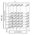
- an image display device 10 includes an image display panel 30 and a signal processing unit 20 .
- an image display device assembly according to the first embodiment includes the image display device 10 , and a planar light source device 50 which irradiates the image display device (specifically, image display panel 30 ) from the back.
- the image display panel 30 is configured of P 0 ⁇ Q 0 pixels (P 0 pixels in the horizontal direction, Q 0 pixels in the vertical direction) being arrayed in a two-dimensional matrix shape each of which is configured of a first sub-pixel for displaying a first primary color (e.g., red, which can be applied to later-described various embodiments) (indicated by “R”), a second sub-pixel for displaying a second primary color (e.g., green, which can be applied to later-described various embodiments) (indicated by “G”), a third sub-pixel for displaying a third primary color (e.g., blue, which can be applied to later-described various embodiments) (indicated by “B”), and a fourth sub-pixel for displaying a fourth color (specifically, white, which can be applied to later-described various embodiments) (indicated by “W”).
- a first primary color e.g., red, which can be applied to later-described various embodiments
- the image display device is configured of, more specifically, a transmissive color liquid crystal display device
- the image display panel 30 is configured of a color liquid crystal display panel, and further includes a first color filter, which is disposed between the first sub-pixels R and the image observer, for passing the first primary color, a second color filter, which is disposed between the second sub-pixels G and the image observer, for passing the second primary color, and a third color filter, which is disposed between the third sub-pixels B and the image observer, for passing the third primary color. Note that no color filter is provided to the fourth sub-pixel W.
- a transparent resin layer may be provided instead of a color filter, and thus, a great step can be prevented from occurring with the fourth sub-pixel W by omitting a color filter. This can be applied to later-described various embodiments.
- the first sub-pixels R, second sub-pixels G, third sub-pixels B, and fourth sub-pixels W are arrayed with an array similar to a diagonal array (mosaic array).
- the first sub-pixels R, second sub-pixels G, third sub-pixels B, and fourth sub-pixels W are arrayed with an array similar to a stripe array.
- the signal processing unit 20 includes an image display panel driving circuit 40 for driving the image display panel (more specifically, color liquid crystal display panel), and a planar light source control circuit 60 for driving a planar light source device 50
- the image display panel driving circuit 40 includes a signal output circuit 41 and a scanning circuit 42 .
- a switching device e.g., TFT
- the signal output circuit 41 video signals are held, and sequentially output to the image display panel 30 .
- the signal output circuit 41 and the image display panel 30 are electrically connected by wiring DTL, and the scanning circuit 42 and the image display panel 30 are electrically connected by wiring SCL. This can be applied to later-described various embodiments.
- a first sub-pixel input signal of which the signal value is x 1-(p, q) , a second sub-pixel input signal of which the signal value is x 2-(p, q) , and a third sub-pixel input signal of which the signal value is x 3-(p, q) are input to the signal processing unit 20 according to the first embodiment, and the signal input unit 20 outputs a first sub-pixel output signal of which the signal value is x 1-(p, q) for determining the display gradation of the first sub-pixel R, a second sub-pixel output signal of which the signal value is x 2-(p, q) for determining the display gradation of the second sub-pixel G, a third sub-pixel output signal of which the signal value is x 3-(p, q) for determining the display gradation of the third sub-pixel B, and a fourth sub-
- the maximum value V max of luminosity with the saturation S in the HSV color space enlarged by adding the fourth color (white) as a variable is stored in the signal processing unit 20 . That is to say, the dynamic range of the luminosity in the HSV color space is widened by adding the fourth color (white).
- the signal processing unit 20 obtains a first sub-pixel output signal (signal value x 1-(p, q) ) based on at least the first sub-pixel input signal (signal value x 1-(p, q) ) and the extension coefficient ⁇ 0 to output to the first sub-pixel R, obtains a second sub-pixel output signal (signal value x 2-(p,q) based on at least the second sub-pixel input signal (signal value X 2-(p, q) ) and the extension coefficient ⁇ 0 to output to the second sub-pixel G, obtains a third sub-pixel output signal (signal value x 3-(p, q) ) based on at least the third sub-pixel input signal (signal value x 3-(p, q) and the extension coefficient ⁇ 0 to output to the third sub-pixel B, and obtains a fourth sub-pixel output signal (signal value x 4-(p, q) ) based on at least the first sub-pixel input signal
- the signal processing unit 20 obtains a first sub-pixel output signal based on at least the first sub-pixel input signal and the extension coefficient ⁇ 0 , and the fourth sub-pixel output signal, obtains a second sub-pixel output signal based on at least the second sub-pixel input signal and the extension coefficient ⁇ 0 , and the fourth sub-pixel output signal, and obtains a third sub-pixel output signal based on at least the third sub-pixel input signal and the extension coefficient ⁇ 0 , and the fourth sub-pixel output signal.
- the signal processing unit 20 can obtain the first sub-pixel output signal value X 1-(p, q) , the second sub-pixel output signal value x 2-(p, q) , and the third sub-pixel output signal value x 3-(p, q) , as to the (p, q)'th pixel (or a set of the first sub-pixel R, the second sub-pixel G, and the third sub-pixel B) from the following expressions.
- the signal processing unit 20 further obtains the maximum value V max of the luminosity with the saturation S in the HSV color space enlarged by adding the fourth color as a variable, and further obtains a reference extension coefficient ⁇ 0-std based on the maximum value V max , and determines the extension coefficient ⁇ 0 at each pixel from the reference extension coefficient ⁇ 0-std , an input signal correction coefficient k IS based on the sub-pixel input signal value and an external light intensity correction coefficient k OL , based on external light intensity at each pixel.
- Max represents the maximum value of the three of a first sub-pixel input signal value, a second sub-pixel input signal value, and a third sub-pixel input signal value as to a pixel
- Min represents the minimum value of the three of a first sub-pixel input signal value, a second sub-pixel input signal value, and a third sub-pixel input signal value as to a pixel.
- the extension coefficient ⁇ 0 is determined.
- ⁇ 0 ⁇ 0-std ⁇ ( k IS ⁇ k OL +1) [i]
- the input signal correction coefficient k IS is represented with a function with the sub-pixel input signal values at each pixel as parameters, and specifically a function with the luminosity V(S) at each pixel as a parameter. More specifically, as shown in FIG.
- this function is a downward protruding monotonically decreasing function wherein when the value of the luminosity V(S) is the maximum value, the value of the input signal correction coefficient k IS is the minimum value (“0”), and when the value of the luminosity V(S) is the minimum value, the value of the input signal correction coefficient k IS is the maximum value.
- ⁇ 0 in the left-hand side in Expression [ii] has to be expressed as “ ⁇ 0-(p, q) ” in a precise sense, but is expressed as “ ⁇ 0 ” for convenience of description. That is to say, the expression “ ⁇ 0 ” is equal to the expression “ ⁇ 0-(p, q) ”.
- ⁇ 0 ⁇ 0-std ⁇ ( k IS-(p,q) ⁇ k OL +1) [ii]
- the external light intensity correction coefficient k OL is a constant depending on external light intensity.
- the value of the external light intensity correction coefficient k OL may be selected, for example, by the user of the image display device using a changeover switch or the like provided to the image display device, or by the image display device measuring external light intensity using an optical sensor provided to the image display device, and based on a result thereof, selecting the value of the external light intensity correction coefficient k OL .
- a function of the input signal correction coefficient k IS is suitably selected, whereby, for example, increase in the luminance of a pixel at from intermediate gradation to low gradation can be realized, and on the other hand, gradation deterioration at high-gradation pixels can be suppressed, and also a signal exceeding the maximum luminance can be prevented from being output to a high-gradation pixel, and additionally, the value of the external light intensity correction coefficient k OL is suitably selected, whereby correction according to external light intensity can be performed, and visibility of an image displayed on the image display device can be prevented in a surer manner from deteriorating even when external light irradiates the image display device.
- the input signal correction coefficient k IS and external light intensity correction coefficient k OL should be determined by performing various tests, such as an evaluation test relating to deterioration in the visibility of an image displayed on the image display device when external light irradiates the image display device, and so forth. Also, the input signal correction coefficient k IS and external light intensity correction coefficient k OL should be stored in the signal processing unit 20 as a kind of table, or a lookup table, for example.
- the signal value X 4-(p, q) can be obtained based on the product between Min (p, q) and the extension coefficient ⁇ 0 obtained from Expression [ii].
- the signal value x 4-(p, q) can be obtained based on the above-described Expression (1-1), and more specifically, can be obtained based on the following expression.
- X 4-(p,q) Min (p,q) ⁇ 0 / ⁇ (11)
- Expression (11) the product between Min (p, q) and the extension coefficient ⁇ 0 is divided by ⁇ , but a calculation method thereof is not restricted to this.
- the reference extension coefficient ⁇ 0-std is determined for each image display frame.
- Max (p, q) is the maximum value of three sub-pixel input signal values of (x 1-(p,q) , x 2-(p, q) , x 3-(p, q) ), and Min (p, q) is the minimum value of three sub-pixel input signal values of (X 1-(p, q) , x 2-(p, q) , x 3-(p, q) ).
- the number of display gradation bits is set to 8 bits (the value of display gradation is specifically set to 0 through 255). This can also be applied to the following embodiments.
- FIGS. 4C and 4D schematically illustrate a conceptual view of the HSV color space of a cylinder enlarge by adding the fourth color (white) according to the first embodiment, and a relation between the saturation S and the luminosity V(S). No color filter is disposed in the fourth sub-pixel W where white is displayed.
- white having the maximum luminance is displayed by the group of the first sub-pixel R, the second sub-pixel G, and the third sub-pixel B, and the luminance of such white is represented with BN 1-3 .
- V max can be represented by the following expressions.
- the thus obtained maximum value V max of the luminosity with the saturation S in the HSV color space enlarged by adding the fourth color as a variable is, for example, stored in the signal processing unit 20 as a kind of lookup table, or obtained at the signal processing unit 20 every time.
- the reference extension coefficient ⁇ 0-std should be obtained without including such a pixel or pixel group. This can also be applied to the following embodiments.
- the signal processing unit 20 obtains, based on sub-pixel input signal values of multiple pixels, the saturation S and the luminosity V(S) of these multiple pixels. Specifically, the signal processing unit 20 obtains S (p, q) and V(S) (p, q) from Expression (12-1) and Expression (12-2) based on the first sub-pixel input signal value x 1-(p, q) , the second sub-pixel input signal value x 2-(p, q) , and the third sub-pixel input signal value x 3-(p, q) as to the (p, q)'th pixel. The signal processing unit 20 performs this processing as to all of the pixels. Further, the signal processing unit 20 obtains the maximum value V max of luminosity.
- the signal processing unit 20 obtains the reference extension coefficient ⁇ 0-std based on the maximum value V max . Specifically, of the values of V max /V(S) (p, q) [ ⁇ (S) (p, q) ] obtained at multiple pixels, the smallest value ( ⁇ min ) is taken as the reference extension coefficient ⁇ 0-std .
- the signal processing unit 20 obtains the signal value X 4-(p, q) at the (p, q)'th pixel based on at least the signal value X 1-(p, q) , the signal value X 2-(p, q) , and the signal value X 3-(p, q) .
- the signal value X 4-(p, q) is determined based on Min (p, q) , extension coefficient ⁇ 0 , and constant ⁇ .
- the signal processing unit 20 obtains the signal value X 1-(p, q) at the (p, q)'th pixel based on the signal value x 1-(p, q) , extension coefficient ⁇ 0 , and signal value X 4-(p, q) , obtains the signal value X 2-(p, q) at the (p, q)'th pixel based on the signal value x 2-(p, q) , extension coefficient ⁇ 0 , and signal value X 4-(p, q) , and the signal value X 3-(p, q) at the (p, q)'th pixel based on the signal value x 3-(p, q) , extension coefficient ⁇ 0 , and signal value x 4-(p, q) .
- the signal value X 1-(p, q) , signal value X 2-(p, q) , and signal value X 3-(p, q) at the (p, q)'th pixel are, as described above, obtained based on the following expressions.
- X 1-(p,q) ⁇ 0 ⁇ x 1-(p,q) ⁇ x 4-(p,q) (1-A)
- X 2-(p,q) ⁇ 0 ⁇ x 2-(p,q) ⁇ x 4-(p,q) (1-B)
- X 3-(p,q) ⁇ 0 ⁇ x 3-(p,q) ⁇ x 4-(p,q) (1-C)
- FIGS. 5A and 5B schematically illustrating a relation between the saturation S and luminosity V(S) in the HSV color space of a cylinder enlarged by adding the fourth color (white) according to the first embodiment
- the value of the saturation S providing ⁇ 0 is indicated with “S′”
- the luminosity V(S) at the saturation S′ is indicated with “V(S′)”
- V max is indicated with “V max ′”.
- V(S) is indicated with a black round mark
- V(S) ⁇ 0 is indicated with a white round mark
- V max at the saturation S is indicated with a white triangular mark.
- FIG. 6 illustrates an example of the HSV color space in the past before adding the fourth color (white) according to the first embodiment, the HSV color space enlarged by adding the fourth color (white), and a relation between the saturation S and luminosity V(S) of an input signal.
- FIG. 7 illustrates an example of the HSV color space in the past before adding the fourth color (white) according to the first embodiment, the HSV color space enlarged by adding the fourth color (white), and a relation between the saturation S and luminosity V(S) of an output signal (subjected extension processing). Note that the value of the saturation S of the lateral axis in FIGS. 6 and 7 is originally a value between 0 through 1, but the value is displayed by 255 times of the original value.
- the important point is, as shown in Expression (11), that the value of Min (p, q) is extended by ⁇ 0 .
- the value of Min (p, q) is extended by ⁇ 0 , and accordingly, not only the luminance of the white display sub-pixel (the fourth sub-pixel W) but also the luminance of the red display sub-pixel, green display sub-pixel, and blue display sub-pixel (first sub-pixel R, second sub-pixel G, and third sub-pixel B) are increased as shown in Expression (1-A), Expression (1-B), and Expression (1-C). Accordingly, change in color can be suppressed, and also occurrence of a problem wherein dullness of a color occurs can be prevented in a sure manner.
- the value of Min (p, q) is extended by ⁇ 0 , and accordingly, the luminance of the pixel is extended ⁇ 0 times. Accordingly, this is optimum, for example, in a case where image display of still images or the like can be performed with high luminance.
- output signal values (X 1-(p, g) , X 2-(p, q) , X 3-(p, q) , x 4-(p, q) ) to be output in the event that the values shown in the following Table 2 are input as input signal values (x 1-(p, q) , x 2-(p, q) , x 3-(p, q) will be shown in the following Table 2.
- third sub-pixel output signal value X 3-(p, q) 0
- the signal value x 4-(p, q) , signal value x 2-(p, q) , signal value x 3-(p, q) at the (p, q)'th pixel are extended based on the reference extension coefficient ⁇ 0-std . Therefore, in order to have generally the same luminance as the luminance of an image in an unextended state, the luminance of the planar light source device 50 should be decreased based on the reference extension coefficient ⁇ 0-std . Specifically, the luminance of the planar light source device 50 should be enlarged by 1(1/ ⁇ 0-std ) times. Thus, reduction in the power consumption of the planar light source device can be realized.
- FIGS. 8A and 8B are diagrams schematically illustrating the input signal values and output signal values according to the image display device driving method and the image display device assembly driving method according to the first embodiment, and the processing method disclosed in Japanese Patent No. 3805150.
- FIG. 8A the input signal values of the first sub-pixel R, second sub-pixel G, and third sub-pixel B are shown in [1].
- a state in which the extension processing is being performed (an operation for obtaining product between an input signal value and the extension coefficient ⁇ 0 ) is shown in [2]. Further, a state after the extension processing was performed (a state in which the output signal values X 1-(p, q) , X 2-(p, q) , X 3-(p, q) , and X 4-(p, q) have been obtained) is shown in [3].
- the input signal values of a set of the first sub-pixel R, second sub-pixel G, and third sub-pixel B according to the processing method disclosed in Japanese Patent No. 3805150 are shown in [4]. Note that these input signal values are the same as shown in [1] in FIG. 8A .
- the digital values Ri, Gi, and Bi of a sub-pixel for red input, a sub-pixel for green input, and a sub-pixel for blue input, and a digital value W for driving a sub-pixel for luminance are shown in [5]. Further, the obtained result of each value of Ro, Go, Bo, and W is shown in [6]. According to
- FIGS. 8A and 8B with the image display device driving method and the image display device assembly driving method according to the first embodiment, the maximum realizable luminance is obtained at the second sub-pixel G.
- the processing method disclosed in Japanese Patent No. 3805150 it turns out that the luminance has not reached the maximum realizable luminance at the second sub-pixel G.
- image display at higher luminance can be realized.
- the reference extension coefficient ⁇ 0-std may be determined such that a ratio of pixels where the value of the luminosity obtained from the product between the luminosity V(S) and the reference extension coefficient ⁇ 0-std and extended exceeds the
- Process 130 and Process 140 should be executed.
- the value of ⁇ (S) exceeds 1.0 and also concentrates on 1.0 neighborhood. Accordingly, in the event that the minimum value of ⁇ (S) is taken as the reference extension coefficient ⁇ 0-std , the extension level of the output signal value is small, and there may often be caused a case where it becomes difficult to achieve low consumption power of the image display device assembly. Therefore, for example, the value of ⁇ 0 is set to 0.003 through 0.05, whereby the value of the reference extension coefficient ⁇ 0-std can be increased, and thus, the luminance of the planar light source device 50 should be set (1/ ⁇ 0 -std) times, and accordingly, low consumption power of the image display device assembly can be achieved.
- Process 130 and Process 140 should be executed.
- Process 130 and Process 140 should be executed.
- the reference extension coefficient ⁇ 0-std may be set to a predetermined value ⁇ 0-std or less (e.g., specifically, 1.3 or less).
- Expression (17-1) through Expression (17-6) are used, whereby whether or not yellow is greatly mixed in the color of an image can be determined with a little computing amount, the circuit scale of the signal processing unit 20 can be reduced, and reduction in computing time can be realized.
- the coefficients and numeric values in Expression (17-1) through Expression (17-6) are not restricted to these.
- determination can be made with smaller computing amount by using higher order bits alone, and further reduction in the circuit scale of the signal processing unit 20 can be realized.
- the reference extension coefficient ⁇ 0-std is set to the predetermined value or less (e.g., specifically, 1.3 or less).
- Expression (14) and the value range of ⁇ 0 according to the image display device driving method according to the first mode of the present disclosure which have been described in the first embodiment, Expression (15-1) and Expression (15-2) according to the image display device driving method according to the sixth mode of the present disclosure, Expression (16-1) through Expression (16-5) according to the image display device driving method according to the eleventh mode of the present disclosure, or alternatively, the stipulations of Expression (17-1) through Expression (17-6) according to the image display device driving method according to the sixteenth mode of the present disclosure, or alternatively, the stipulations according to the image display device driving method according to the twenty-first mode of the present disclosure can also be applied to the following embodiments.
- a second embodiment is a modification of the first embodiment.
- a direct-type planar light source device according to the related art may be employed, but with the second embodiment, a planar light source device 150 of a split driving method (partial driving method) which will be described below is employed.
- split driving method partial driving method
- FIG. 9 A conceptual view of an image display panel and a planar light source device making up an image display device assembly according to the second embodiment is shown in FIG. 9 , a circuit diagram of a planar light source device control circuit according to the planar light source device making up the image display device assembly is shown in FIG. 10 , and the layout and array state of a planar light source unit and so forth according to the planar light source device making up the image display device assembly are schematically shown in FIG. 11 .
- the planar light source device 150 of the split driving method is made up of, when assuming that a display region 131 of an image display panel 130 making up a color liquid crystal display device has been divided into S ⁇ T virtual display region units 132 , S ⁇ T planar light source units 152 corresponding to these S ⁇ T display region units 132 , and the emission states of the S ⁇ T planar light source units 152 are individually controlled.
- the image display panel (color liquid crystal display panel) 130 includes a display region 131 of P ⁇ Q pixels in total of P pixels in a first direction, and Q pixels in a second direction being arrayed in a two-dimensional matrix shape.
- the display region 131 has been divided into S ⁇ T virtual display region units 132 .
- Each display region unit 132 is configured of multiple pixels.
- the HD-TV stipulations are satisfied as resolution for image display, and when the number of pixels P ⁇ Q arrayed in a two-dimensional matrix shape is represented with (P, Q), the resolution for image display is (1920, 1080), for example.
- the display region 131 made up of the pixels arrayed in a two-dimensional matrix shape is divided into S ⁇ T virtual display region units 132 (boundaries are indicated with dotted lines).
- the values of (S, T) are (19, 12), for example.
- the number of the display region units 132 (and later-described planar light source units 152 ) in FIG. 9 differs from this value.
- Each display region unit 132 is made up of multiple pixels, and the number of pixels making up one display region unit 132 is around 10000, for example.
- the image display panel 130 is line-sequentially driven.
- the image display panel 130 includes scanning electrodes (extending in the first direction) and data electrodes (extending in the second direction) which intersect in a matrix shape, inputs a scanning signal from the scanning circuit to a scanning electrode to select and scan the scanning electrode, and displays an image based on the data signal (output signal) input to a data electrode from the signal output circuit, thereby making up one screen.
- the direct-type planar light source device (backlight) 150 is configured of S ⁇ T planar light source units 152 corresponding to these S ⁇ T virtual display region units 132 , and each planar light source unit 152 irradiates the display region unit 132 corresponding to thereto from the back face.
- the light source provided to the planar light source units 152 is individually controlled. Note that the planar light source device 150 is positioned below the image display panel 130 , but in FIG. 9 the image display panel 130 and the planar light source device 150 are separately displayed.
- the display region 131 made up of pixels arrayed in a two-dimensional matrix shape is divided into S ⁇ T display region units 132 , if this state is expressed with “row” ⁇ “column”, it can be said that the display region 131 is divided into T-row ⁇ S-column display region units 132 . Also, though a display region unit 132 is made up of multiple (M 0 ⁇ N 0 ) pixels, if this state is expressed with a display region unit 132 is made up of M 0 -row ⁇ N 0 -column pixels.
- a light sources is made up of a light emitting diode 153 which is driven based on the pulse width modulation (PWM) control method.
- PWM pulse width modulation
- Increase/decrease in the luminance of a planar light source unit 152 is performed by increase/decrease control of a duty ratio according to the pulse width modulation control of the light emitting diode 153 making up the planar light source unit 152 .
- the irradiation light emitted from the light emitting diode 153 is emitted from the planar light source unit 152 via a light diffusion plate, passed through an optical function sheet group such as an optical diffusion sheet, a prism sheet, or a polarization conversion sheet (not shown in the drawing), and irradiated on the image display panel 130 from the back face.
- One optical sensor photodiode 67
- the luminance and chromaticity of a light emitting diode 153 are measured by a photodiode 67 .
- the planar light source device driving circuit 160 for driving the planar light source units 152 performs on/off control of a light emitting diode 153 making up a planar light source unit 152 based on the planar light source control signal (driving signal) from the signal processing unit 20 based on the pulse width modulation control method.
- the planar light source device driving circuit 160 is configured of an arithmetic circuit 61 , a storage device (memory) 62 , an LED driving circuit 63 , a photodiode control circuit 64 , a switching device 65 made up of an FET, and an LED driving power source (constant current source) 66 . These circuits and so forth making up the planar light source device control circuit 160 may be familiar circuits and so forth.
- a feedback mechanism is formed such that the emitting state of a light emitting diode 153 in a certain image display frame is measured by a photodiode 67 , and the output from the photodiode 67 is input to the photodiode control circuit 64 , and taken as data (signal) serving as luminance and chromaticity of the light emitting diode 153 at the photodiode control circuit 64 , and arithmetic circuit 61 for example, and such data is transmitted to the LED driving circuit 63 , and the emitting state of a light emitting diode 153 in the next image display frame is controlled.
- a resistive element r for current detection is inserted downstream of the light emitting diode 153 in series with the light emitting diode 153 , current flowing into the resistive element r is converted into voltage, the operation of the LED driving poser source 66 is controlled such that voltage drop at the resistive element r has a predetermined value, under the control of the LED driving circuit 63 .
- FIG. 10 illustrates three sets of planar light source units 152 . In FIG. 10 , a configuration is shown wherein one light emitting diode 153 is provided to one planar light source unit 152 , but the number of the light emitting diodes 153 making up one planar light source unit 152 is not restricted to one.
- Each pixel is configured, as described above, with four types of sub-pixels of a first sub-pixel R, a second sub-pixel G, a third sub-pixel B, and a fourth sub-pixel W as one set.
- control of the luminance (gradation control) of each sub-pixel is taken as 8-bit control, which will be performed by 2 8 steps of 0 through 255.
- the value PS of a pulse width modulation output signal for controlling the emitting time of each of the light emitting diodes 153 making up each planar light source unit 152 is also taken the value of 2 8 steps of 0 through 255.
- the gradation control may be taken as 10-bit control, and performed by 2 10 steps of 0 through 1023, and in this case, an expression with a 8-bit numeric value should be changed to four times thereof, for example.
- the light transmittance (also referred to as aperture ratio) Lt of a sub-pixel, the luminance (display luminance) y of the portion of a display region corresponding to the sub-pixel, and the luminance (light source luminance) Y of a planar light source unit 152 are defined as follows.
- Y 1 is the highest luminance of light source luminance for example, and hereafter may also be referred to as a light source luminance first stipulated value.
- Lt 2 is the maximum value of the light transmittance (numerical aperture) of a sub-pixel at a display region unit 132 for example, and hereafter may also be referred to as a light transmittance first stipulated value.
- Lt 2 is the maximum value of the light transmittance (numerical aperture) of a sub-pixel when assuming that a control signal equivalent to an intra-display region unit signal maximum value X max-(s, t) that is the maximum value of the output signals from the signal processing unit 20 to be input to the image display panel driving circuit 40 for driving all of the sub-pixels making up a display region unit 132 has been supplied to a sub-pixel, and hereafter may also be referred to as a light transmittance second stipulated value.
- 0 ⁇ Lt 2 ⁇ Lt 1 should be satisfied.
- y 2 is display luminance to be obtained when assuming that light source luminance is a light source luminance first stipulated value Y 1 , and the light transmittance (numerical aperture) of a sub pixel is the light transmittance second stipulated value, and hereafter may also be referred to as a display luminance second stipulated value.
- Y 2 is the light source luminance of the planar light source unit 152 for setting the luminance of a sub-pixel to the display luminance second stipulated value (y 2 ) when assuming that a control signal equivalent to the intra-display region unit signal maximum value x max-(s, t) , and moreover, when assuming that the light transmittance (numerical aperture) of a sub-pixel at this time has been corrected to the light transmittance first stipulated value Lt 1 .
- the light source luminance Y 2 may be subjected to correction in which influence of the light source luminance of each planar light source unit 152 to be given to the light source luminance of another planar light source unit 152 is taken into consideration.
- the luminance of a light emitting device making up a planar light source unit 152 corresponding to a display region unit 132 is controlled by the planar light source device control circuit 160 so as to obtain the luminance of a sub-pixel (the display luminance second stipulated Y 2 at the light transmittance first stipulated value Lt 2 ) when assuming that a control signal equivalent to the intra-display region unit signal maximum value x max-(s, t) has been supplied to a sub-pixel at the time of partial driving (split driving) of the planar light source device, but specifically, for example, the light source luminance Y 2 should be controlled (e.g., should be reduced) so as to obtain the display luminance Y 2 at the time of the light transmittance (numerical aperture) being taken as the light transmittance first stipulated value Lt 2 .
- output signals X 1-(p, q) , X 2-(p, q) , X 3-(p, q) , and X 4-(p, q) for controlling the light transmittance Lt of each of the sub-pixels are transmitted from the signal processing unit 20 to the image display panel driving circuit 40 .
- control signals are generated from the output signals, and these control signals are supplied (output) to sub-pixels, respectively.
- each of the control signals, a switching device making up each sub-pixel is driven, desired voltage is applied to a transparent first electrode and a transparent second electrode (not shown in the drawing) making up a liquid crystal cell, and accordingly, the light transmittance (numerical aperture) Lt of each sub-pixel is controlled.
- the greater a control signal the higher the light transmittance (numerical aperture) of a sub-pixel, and the higher the value of the luminance of the portion of a display region corresponding to the sub-pixel (display luminance y) is. That is to say, an image made up of light passing through a sub-pixel (usually, one kind of dotted shape) is bright.
- Control of the display luminance y and light source luminance Y 2 is performed for each image display frame of image display of the image display panel 130 , for each display region unit, and for each planar light source unit. Also, the operation of the image display panel 130 , and the operation of the planar light source device 150 are synchronized. Note that the number of image information to be transmitted to the driving circuit for one second (image per second) as electrical signals is a frame frequency (frame rate), and the reciprocal number of the frame frequency is frame time (unit: seconds).
- extension processing for extending an input signal to obtain an output signal has been performed as to all of the pixels based on one reference extension coefficient ⁇ 0-std .
- a reference extension coefficient ⁇ 0-std is obtained at each of the S ⁇ T display region units 132 , and extension processing based on the reference extension coefficient ⁇ 0-std is performed at each of the display region units 132 .
- the luminance of a light source is set to (1/ ⁇ 0-std-(s, t) ).
- the luminance of a sub-pixel (the display luminance second stipulated value Y 2 at the light transmittance first stipulated value Lt 1 ) when assuming that a control signal equivalent to the intra-display region signal maximum value x max-(s, t) that is the maximum value of the output signal values X 1-(s, t) , X 2-(s, t) , X 3-(s, t) , and X 4-(s, t) from the signal processing unit 20 to be input for driving all of the sub-pixels making up each of the display region units 132 has been supplied to a sub-pixel, the luminance of a light source making up the planar light source unit 152 corresponding to this display region unit 132 is controlled by the planar light source device control circuit 160 .
- the light source luminance Y 2 should be controlled (e.g., should be reduced). That is to say, specifically, the light source luminance Y 2 of the planar light source unit 152 should be controlled for each image display frame so as to satisfy the above-described Expression (A).
- the luminance (light source luminance Y 2 ) requested of the S ⁇ T planar light source units 152 based on the request from Expression (A) will be represented with a matrix [L P ⁇ Q ].
- the luminance of a certain planar light source unit obtained when driving the certain planar light source alone without driving other planar light source units should be obtained as to the S ⁇ T planer light source units 152 beforehand.
- Such luminance will be represented with a matrix [L′ P ⁇ Q ].
- a correction coefficient will be represented with a matrix [ ⁇ P ⁇ Q ].
- a relation between these matrices can be represented by the following Expression (B-1).
- the correction coefficient matrix [ ⁇ P ⁇ Q ] may be obtained beforehand.
- [ L P ⁇ Q ] [L′ P ⁇ Q ] ⁇ [ ⁇ P ⁇ Q ] (B-1)
- the matrix [L′ P ⁇ Q ] should be obtained from Expression (B-1).
- the solution of Expression (B-2) is not an exact solution, and may be an approximate solution.
- the value of a pulse width modulation output signal for controlling the emitting time of the light emitting diode 153 at a planar light source unit 152 can be obtained. Then, based on the value of this pulse width modulation output signal, on-time t ON and off-time t OFF of the light emitting diode 153 making up the planar light source unit 152 should be determined at the planar light source device control circuit 160 .
- t ON +t OFF constant value t Const holds.
- a signal equivalent to the on-time t ON of the light emitting diode 153 making up the planar light source unit 152 is transmitted to the LED driving circuit 63 , and based on the value of the signal equivalent to the on-time t ON from this LED driving circuit 63 , the switching device 65 is in an on state by the on-time t ON , and the LED driving current from the LED driving power source 66 flows into the light emitting diode 153 .
- each light emitting diode 153 emits light by the on-time t ON at one image display frame. In this way, each display region unit 132 is irradiated with predetermined illuminance.
- planar light source device 150 of split driving method (partial driving method) described in the second embodiment may be employed with another embodiment.
- a third embodiment is also a modification of the first embodiment.
- An equivalent circuit diagram of an image display device according to the third embodiment is shown in FIG. 13
- a conceptual view of an image display panel making up the image display device is shown in FIG. 14 .
- the image display device which will be described below is used.
- the image display device includes an image display panel made up of light emitting units UN for displaying a color image being arrayed in a two-dimensional matrix shape, each of which is made up of a first light emitting device for emitting blue (equivalent to first sub-pixel R), a second light emitting device for emitting green (equivalent to second sub-pixel G), a third light emitting device for emitting red (equivalent to third sub-pixel B), and a fourth light emitting device for emitting white (equivalent to fourth sub-pixel W).
- an image display panel having an arrangement and a configuration which will be described below can be given, for example. Note that the number of the light emitting device units UN should be determined based on specifications requested of the image display device.
- the image display panel making up the image display device is an image display panel of direct-view color display of a passive matrix type or active matrix type direct-view color which controls the emitting/non-emitting state of each of a first light emitting device, a second light emitting device, a third light emitting device, and a fourth light emitting device to directly visually recognize each light emitting device, thereby displaying an image, or alternatively, an image display panel of projection-type color display of a passive matrix type or active matrix type which controls the emitting/non-emitting state of each of a first light emitting device, a second light emitting device, a third light emitting device, and a fourth light emitting device to project to the screen, thereby display an image.
- FIG. 13 a circuit diagram including a light emitting panel making up the image display panel of direct-view color display of such an active matrix type is shown in FIG. 13 , and one of electrodes (p-side electrode or n-side electrode) of each light emitting device 210 (in FIG. 13 ), and one of electrodes (p-side electrode or n-side electrode) of each light emitting device 210 (in FIG. 13 ).
- a light emitting device for emitting red is indicated with “R”
- a light emitting device for emitting green is indicated with “G”
- a light emitting device for emitting blue is indicated with “B”
- a light emitting device for emitting white is indicated with “W”
- the driver 233 is connected to a column driver 231 and a row driver 232 .
- the other electrode (n-side electrode or p-side electrode) of each light emitting device 210 is connected to a grounding wire.
- the control of the emitting/non-emitting state of each light emitting device 210 is performed by selection of a driver 233 by the row driver 232 , and a luminance signal for driving each light emitting device 210 is supplied from the column driver 231 to the driver 233 .
- a light emitting device R for emitting red (first light emitting device, first sub-pixel R), a light emitting device G for emitting green (second light emitting device, second sub-pixel G), a light emitting device B for emitting blue (third light emitting device, third sub-pixel B), and a light emitting device W for emitting white (fourth light emitting device, fourth sub-pixel W) is performed by the driver 233 , and the emitting/non-emitting state of each of these light emitting device R for emitting red, light emitting device G for emitting green, light emitting device B for emitting blue, and light emitting device W for emitting white may be controlled by time-sharing, or alternatively, these may be emitted at the same time. Note that the emitting/non-emitting state of each light emitting device is directly viewed at a direct-view image display device, and is projected on the screen via a projection lens at a projection-type image display device.
- FIG. 14 a conceptual view of an image display panel making up such an image display device is shown in FIG. 14 .
- the emitting/non-emitting state of each light emitting device is directly viewed at a direct-view image display device, and is projected on the screen via a projection lens at a projection-type image display device.
- the image display panel making up the image display device according to the third embodiment may be a direct-view-type or projection-type image display panel for color display which includes a light passage control device (light valve, and specifically, for example, a liquid crystal display including a high-temperature polysilicon-type thin-film transistor.
- a light passage control device light valve, and specifically, for example, a liquid crystal display including a high-temperature polysilicon-type thin-film transistor.
- an output signal for controlling the emitting state of each of the first light emitting device (first sub-pixel R), second light emitting device (second sub-pixel G), third light emitting device (first sub-pixel B), and fourth light emitting device (fourth sub-pixel W) should be obtained based on the extension processing described in the first embodiment.
- the luminance can be increased around ⁇ 0-std times (the luminance of each pixel can be increased ⁇ 0 times) as the entire image display device.
- a fourth embodiment relates to the image display device driving method according to the second mode, seventh mode, twelfth mode, seventeenth mode, and twenty-second mode of the present disclosure, and the image display device assembly driving method according to the second mode, seventh mode, twelfth mode, seventeenth mode, and twenty-second mode of the present disclosure.
- a pixel Px made up of a first sub-pixel R for displaying a first primary color (e.g., red), a second sub-pixel G for displaying a second primary color (e.g., green), and a third sub-pixel B for displaying a third primary color (e.g., blue) is arrayed in a two-dimensional matrix shape in the first direction and the second direction.
- a pixel group PG is made up of at least a first pixel Px 2 and a second pixel Px 2 arrayed in the first direction.
- the fourth embodiment if we say that the first direction is the row direction, and the second direction is the column direction, a first pixel Px 1 in the q'th column (where 1 ⁇ q′ ⁇ Q ⁇ 1), and a first pixel Px 1 in the (q′+1)'th column adjoin each other, and a fourth sub-pixel W in the q'th column and a fourth sub-pixel W in the (q′+1)'th column do not adjoin each other. That is to say, the second pixel Px 2 and the fourth sub-pixel W are alternately disposed in the second direction. Note that, in FIG.
- a first sub-pixel R, a second sub-pixel G, and a third sub-pixel B making up the first pixel Px 1 are surrounded by a solid line
- a first sub-pixel R, a second sub-pixel G, and a third sub-pixel B making up the second pixel Px 2 are surrounded by a dotted line.
- FIGS. 16 , 17 , 20 , 21 , and 22 This can also be applied to later-described FIGS. 16 , 17 , 20 , 21 , and 22 . Since the second pixel Px 2 and the fourth sub-pixel W are alternately disposed in the second direction, a streaked pattern can be prevented in a sure manner from being included in an image due to existence of the fourth sub-pixel W though this depends on pixel pitches.
- a first pixel Px (p, q)-1 making up the (p, q)'th pixel group PG (p, q) (where 1 ⁇ p ⁇ P, 1 ⁇ q ⁇ Q)
- a first sub-pixel input signal of which the signal value is x 1-(p, q)-1 a second sub-pixel input signal of which the signal value is x 2-(p, q)-1
- a third sub-pixel input signal of which the signal value is x 3-(p, q)-1 are input to the signal processing unit 20
- a second pixel Px (p, q)-2 making up the (p, q)'th pixel group PG (p, q) a first sub-pixel input signal of which the signal value is x 1-(p, q)-2 , a second sub-pixel input signal of which the signal value is x 2-(p, q)-2
- the signal processing unit 20 outputs, regarding the first pixel Px (p, q)-1 making up the (p, q)'th pixel group PG (p, q) , a first sub-pixel output signal of which the signal value is X 1-(p, q)-1 for determining the display gradation of the first sub-pixel R, a second sub-pixel output signal of which the signal value is X 2-(p, q)-1 for determining the display gradation of the second sub-pixel G, and a third sub-pixel output signal of which the signal value is X 3-(p, q)-1 for determining the display gradation of the third sub-pixel B, and outputs, regarding the second pixel Px (p, q)-2 making up the (p, q)'th pixel group PG (p, q) , a first sub-pixel output signal of which the signal value is X 1-(p, q)-2 for determining the display gradation of the first sub-pixel R
- the signal processing unit 20 obtains the first sub-pixel output signal (signal value X 1-(p, q)-1 ) based on at least the first sub-pixel input signal (signal value x 4-(p, q)-1 ) and the extension coefficient ⁇ 0 to output to the first sub-pixel R, the second sub-pixel output signal (signal value X 2-(p, q)-1 ) based on at least the second sub-pixel input signal (signal value x 2-(p, q)-1 ) and the extension coefficient ⁇ 0 to output to the second sub-pixel G, and the third sub-pixel output signal (signal value X 3-(p, q)-1 ) based on at least the third sub-pixel input signal (signal value X 3-(p, q)-1) and the extension coefficient ⁇ 0 to output to the third sub-pixel B, and regarding the second pixel Px (p, q)-2 , obtains the first sub-pixel output signal (signal value X 1-(p, q)-1
- the signal processing unit 20 obtains, regarding the fourth sub-pixel W, the fourth sub-pixel output signal (signal value X 4-(p, q) ) based on the fourth sub-pixel control first signal (signal value SG 1-(p, q) ) obtained from the first sub-pixel input signal (signal value x 1-(p, q)- 1), second sub-pixel input signal (signal value x 2-(p, q)-1 ), and third sub-pixel input signal (signal value x 3-(p, q)-1 ) as to the first pixel Px (p, q)-1 , and the fourth sub-pixel control second signal (signal value SG 2-(p, q) ) obtained from the first sub-pixel input signal (signal value x 1-(p, q)-2 ), second sub-pixel input signal (signal value x 2-(p, q)-2 ), and third sub-pixel input signal (signal value x 3-(p, q)-2 ) as to the second pixel Px
- the fourth sub-pixel control first signal value SG 2-(p, q) is determined based on Min (p, q)-1 and the extension coefficient ⁇ 0
- the fourth sub-pixel control second signal value SG 2-(p, q) is determined based on Min (p, q)-2 and the extension coefficient ⁇ 0
- Expression (41-1) and Expression (41-2) based on Expression (2-1-1) and Expression (2-1-2) are employed as the fourth sub-pixel control first signal value SG 1-(p, q) and fourth sub-pixel control second signal value SG 2-(p, q) .
- SG 1-(p,q) Min (p,q)-1 ⁇ 0 (41-1)
- SG 2-(p,q) Min (p,q)-2 ⁇ 0 (41-2)
- the first sub-pixel output signal is obtained based on at least the first sub-pixel input signal and the extension coefficient ⁇ 0 , but the first sub-pixel output signal value x 1-(p, q)-1 is obtained based on the first sub-pixel input signal value x 1-(p, q)-1 , extension coefficient ⁇ 0 , fourth sub-pixel control first signal value SG 1-(p, q) and constant ⁇ , i.e., [ x 1-(p,q)-1 , ⁇ 0 ,SG 1-(p,q) , ⁇ ], the second sub-pixel output signal is obtained based on at least the second sub-pixel input signal and the extension coefficient ⁇ 0 , but the second sub-pixel output signal value X 2-(p, q)-1 is obtained based on the second sub-pixel input signal value x 2-(p, q)-1 , extension coefficient ⁇ 0 , fourth sub-pixel control first signal value SG 1-(p
- the output signal values X 1-(p, q)-1 , X 2-(p, q)-1 , X 3-(p, q)-1 , X 1-(p, q)-2 , X 2-(p, q)-2 , and X 3-(p, q)-2 can be determined, as described above, based on the extension coefficient ⁇ 0 and constant ⁇ , and more specifically can be obtained from the following expressions.
- X 1-(p,q)-1 ⁇ 0 ⁇ x 1-(p,q)-1 ⁇ SG 1-(p,q) (2-A)
- X 2-(p,q)-1 ⁇ 0 ⁇ x 2-(p,q)-1 ⁇ SG 1-(p,q) (2-B)
- X 3-(p,q)-1 ⁇ 0 ⁇ x 3-(p,q)-1 ⁇ SG 1-(p,q) (2-C)
- X 1-(p,q)-2 ⁇ 0 ⁇ x 1-(p,q)-2 ⁇ SG 2-(p,q) (2-D)
- X 2-(p,q)-2 ⁇ 0 ⁇ x 2-(p,q)-2 ⁇ SG 2-(p,q) (2-E)
- X 3-(p,q)-2 ⁇ 0 ⁇ x 3-(p,q)-2 ⁇ SG 2-(p,q) (2-F)
- the signal value X 4-(p, q) is obtained by the following arithmetic average Expression (42-1) and Expression (42-2) based on Expression (2-11).
- Expression (42-1) and Expression (42-2) (Min (p,q)-1 ⁇ 0 +Min (p,q)-2 ⁇ 0 )/(2 ⁇ ) (42-2)
- the reference extension coefficient ⁇ 0-std is determined for each image display frame. Also, the luminance of the planar light source device 50 is decreased based on the reference extension coefficient ⁇ 0-std . Specifically, the luminance of the planar light source device 50 should be enlarged by (1/ ⁇ 0-std ) times.
- the maximum value V max (S) of luminosity with the saturation S in the HSV color space enlarged by adding the fourth color (white) as a variable is stored in the signal processing unit 20 . That is to say, the dynamic range of the luminosity in the HSV color space is widened by adding the fourth color (white).
- the following processing will be performed so as to maintain a ratio between the luminance of a first primary color displayed with (first sub-pixel R+ fourth sub-pixel W), the luminance of a second primary color displayed with (second sub-pixel G+ fourth sub-pixel W), and the luminance of a third primary color displayed with (third sub-pixel B+ fourth sub-pixel W) as the entirety of the first pixel and second pixel, i.e., at each pixel group.
- the following processing will be performed so as to keep (maintain) color tone, and further so as to keep (maintain) gradation-luminance property (gamma property, ⁇ property).
- the signal processing unit 20 obtains the saturation S and luminosity V(S) at multiple pixel groups PG (p, q) based on sub-pixel input signal values at multiple pixels. Specifically, the signal processing unit 20 obtains S (p, q)-1 , S (p, q)-2 , V(S) (p, q)-1 , and V(S) (p, q)-2 from Expression (43-1) through Expression (43-4) based on first sub-pixel input signal values x 1-(p, q)-1 and x 1-(p, q)-2 , second sub-pixel input signal values x 2-(p, q)-1 and x 2-(p, q)-2 , and third sub-pixel input signal values x 3-(p, q)-1 and x 3-(p, q)-2 as to the (p, q)'th pixel group PG (p, q) .
- the signal processing unit 20 performs this processing as to all of the pixel groups PG (p, q) .
- S (p,q)-1 (Max (p,q)-1 ⁇ Min (p,q)-1 )/Max (p,q)-1 (43-1)
- V ( S ) (p,q)-1 Max (p,q)-1 (43-2)
- S (p,q)-2 (Max (p,q)-2 ⁇ Min (p,q)-2 )/Max (p,q)-2 (43-3)
- V ( S ) (p,q)-2 Max (p,q)-2 (43-4)
- Process 410 (Max (p,q)-1 ⁇ Min (p,q)-1 )/Max (p,q)-1 (43-1)
- V ( S ) (p,q)-1 Max (p,q)-1 (43-2)
- S (p,q)-2 (Max (p,q)-2 ⁇ Min (p,q)-2 )/Max (p,q)-2 (43-3)
- the signal processing unit 20 determines, in the same way as with the first embodiment, the reference extension coefficient ⁇ 0-std and extension coefficient ⁇ 0 from ⁇ min or a predetermined ⁇ 0 ), or alternatively, based on the stipulations of Expression (15-2), or Expressions (16-1) through (16-5), or Expressions (17-1) through (17-6), for example.
- the signal processing unit 20 then obtains a signal value X 4-(p, q) at the (p, q)'th pixel group PG (p, q) based on at least input signal values x 1-(p, q)-1 , x 2-(p, q)-1 , x 3-(p, q)-1 , x 1-(p, q)-2 , x 2-(p, q)-2 , and x 3-(p, q)-3 .
- the signal value X 4-(p, q) is determined based on Min (p, q)-1 , Min (p, q)-2 , extension coefficient ⁇ 0 , and constant X.
- the signal processing unit 20 obtains the signal value x 1-(p, q)-1 at the (p, q)'th pixel group PG (p, q) based on the signal value x 1-(p, q)-1 , extension coefficient ⁇ 0 , and fourth sub-pixel control first signal SG 1-(p, q) , obtains the signal value X 2-(p, q)-1 based on the signal value x 2-(p, q)-1 , extension coefficient ⁇ 0 , and fourth sub-pixel control first signal SG 1-(p, q) , and obtains the signal value X 3-(p, q)-1 based on the signal value x 3-(p, q)-1 , extension coefficient ⁇ 0 , and fourth sub-pixel control first signal SG 1-(p, q) .
- the signal processing unit 20 obtains the signal value X 1-(p, q)-2 based on the signal value x 1-(p, q)-2 , extension coefficient ⁇ 0 , and fourth sub-pixel control second signal SG 2-(p, q) , obtains the signal value X 2-(p, q)-2 based on the signal value x 2-(p, q)-2 , extension coefficient ⁇ 0 , and fourth sub-pixel control second signal SG 2-(p, q) , and obtains the signal value X 3-(p, q)-2 based on the signal value x 3-(p, q)-2 , extension coefficient ⁇ 0 , and fourth sub-pixel control second signal SG 2-(p, q) .
- Process 420 and Process 430 may be executed at the same time, or Process 420 may be executed after execution of Process 430.
- the signal processing unit 20 obtains the output signal values X 4-(p, q)-1 , X 2-(p, q)-1 , X 3-(p, q)-1 , X 1-(p, q)-2 , X 2-(p, q)-2 , and X 3-(p, q)-2 at the (p, q)'th pixel group PG (p, q) based on Expression (2-A) through Expression (2-F).
- FIG. 19 is a diagram schematically illustrating input signal values and output signal values.
- the input signal values of a set of a first sub-pixel R, a second sub-pixel G, and a third sub-pixel B are shown in [1].
- a state in which the extension processing is being performed an operation for obtaining product between an input signal value and the extension coefficient ad is shown in [2].
- the fourth sub-pixel output signal is obtained based on the fourth sub-pixel control first signal value SG 1-(p, q) and fourth sub-pixel control second signal value SG 2-(p, q) obtained from the first pixel Px 1 of each pixel group PG, and the first sub-pixel input signal, second sub-pixel input signal, and third sub-pixel input signal as to the second pixel Px 2 , and output. That is to say, the fourth sub-pixel output signal is obtained based on the input signals as to the adjacent first pixel Px 1 and second pixel Px 2 , and accordingly, optimization of the output signal as to the fourth sub-pixel W is realized.
- one fourth sub-pixel W is disposed as to a pixel group PG made up of at least the first pixel Px 1 and second pixel Px 2 , whereby decrease in the area of an opening region in a sub-pixel can be suppressed. As a result thereof, increase in luminance can be realized in a sure manner, and also improvement in display quality can be realized.
- the length of a pixel in the first direction is taken as L 1
- the signal values X 1-(p, q)-1 , X 2-(p, q)-1 , X 3-(p, q)-1 , X 1-(p, q)-2 , X 2-(p, q)-2 , X 3-(p, q)-2 may also be obtained based on [ x 1-(p,q)-1 ,x 1-(p,q)-2 , ⁇ 0 ,SG 1-(p,q) , ⁇ ] [ x 2-(p,q)-1 ,x 2-(p,q)-2 , ⁇ 0 ,SG 2-(p,q) , ⁇ ] [ x 3-(p,q)-1 ,x 3-(p,q)-2 , ⁇ 0 ,SG 3-(p,q) , ⁇ ] [ x 1-(p,q)-1 ,x 1-(p,q)-2 , ⁇ 0 ,SG 2-(p,q) , ⁇ ] [ x 2-(p,q)-1 ,x 2-(x)-2 , ⁇
- a fifth embodiment is a modification of the fourth embodiment.
- the array state of a first pixel, a second pixel, and a fourth sub-pixel W is changed.
- the fifth embodiment as schematically shown in the layout of pixels in FIG. 16 , if we say that the first direction is taken as the row direction, and the second direction is taken as the column direction, a first pixel Px 1 in the q'th column (where 1 ⁇ q′ ⁇ Q ⁇ 1), and a second pixel Px 2 in the (q′+1)'th column adjoin each other, and a fourth sub-pixel W in the q'th column and a fourth sub-pixel W in the (q′+1)'th column do not adjoin each other.
- the image display panel, image display device driving method, image display device assembly, and driving method thereof according to the fifth embodiment are the same as those according to the fourth embodiment, and accordingly, detailed description thereof will be omitted.
- a sixth embodiment is also a modification of the fourth embodiment.
- the array state of a first pixel, a second pixel, and a fourth sub-pixel W is changed.
- the sixth embodiment as schematically shown in the layout of pixels in FIG. 17 , if we say that the first direction is taken as the row direction, and the second direction is taken as the column direction, a first pixel Px 1 in the q'th column (where 1 ⁇ q′ ⁇ Q ⁇ 1), and a first pixel Px 1 in the (q′+1)'th column adjoin each other, and a fourth sub-pixel W in the q'th column and a fourth sub-pixel W in the (q′+1)'th column adjoin each other.
- the first sub-pixel R, the second sub-pixel G, the third sub-pixel G, and the fourth sub-pixel W are arrayed in an array similar to a stripe array.
- the image display panel, image display device driving method, image display device assembly, and driving method thereof according to the sixth embodiment are the same as those according to the fourth embodiment, and accordingly, detailed description thereof will be omitted.
- a seventh embodiment relates to an image display device driving method according to the third mode, eight mode, thirteenth mode, eighteenth mode, and twenty-third mode of the present disclosure, and an image display device assembly driving method according to the third mode, eight mode, thirteenth mode, eighteenth mode, and twenty-third mode of the present disclosure.
- the layout of each pixel and pixel group in an image display panel according to the seventh embodiment are schematically shown in FIGS. 20 and 21 .
- an image display panel configured of pixel groups PG being arrayed in a two-dimensional matrix shape in total of P ⁇ Q pixel groups of P pixel groups in the first direction, and Q pixel groups in the second direction.
- Each of the pixel groups PG is made up of a first pixel and a second pixel in the first direction.
- a first pixel Px 1 is made up of a first sub-pixel R for displaying a first primary color (e.g., red), a second sub-pixel G for displaying a second primary color (e.g., green), and a third sub-pixel B for displaying a third primary color (e.g., blue), and a second pixel Px 2 is made up of a first sub-pixel R for displaying a first primary color (e.g., red), a second sub-pixel G for displaying a second primary color (e.g., green), and a fourth sub-pixel W for displaying a fourth color (e.g., white).
- a first primary color e.g., red
- a second sub-pixel G for displaying a second primary color (e.g., green)
- a fourth sub-pixel W for displaying a fourth color (e.g., white).
- a first pixel Px 1 is made up of a first sub-pixel R for displaying a first primary color, a second sub-pixel G for displaying a second primary color, and a third sub-pixel B for displaying a third primary color being sequentially arrayed
- a second pixel Px 2 is made up of a first sub-pixel R for displaying a first primary color, a second sub-pixel G for displaying a second primary color, and a fourth sub-pixel W for displaying a fourth color being sequentially arrayed.
- a third sub-pixel B making up a first pixel Px 1 , and a first sub-pixel R making up a second pixel Px 2 adjoin each other.
- a fourth sub-pixel W making up a second pixel Px 2 , and a first sub-pixel R making up a first pixel Px 1 in a pixel group adjacent to this pixel group adjoin each other.
- a sub-pixel has a rectangle shape, and is disposed such that the longer side of this rectangle is parallel to the second direction, and the shorter side is parallel to the first direction.
- a third sub-pixel B is taken as a sub-pixel for displaying blue. This is because the visibility of blue is around 1 ⁇ 6 as compared to the visibility of green, and even if the number of sub-pixels for displaying blue is taken as a half of pixels groups, no great problem occurs. This can also be applied to later-described eight and tenth embodiments.
- the image display device and image display device assembly according to the seventh embodiment may be taken as the same as one of the image display device and image display device assembly described in the first through third embodiments.
- an image display device 10 according to the seventh embodiment also includes an image display panel and a signal processing unit 20 , for example.
- the image display device assembly according to the seventh embodiment includes the image display device 10 , and a planer light source device 50 for irradiating the image display device (specifically, image display panel) from the back face.
- the signal processing unit 20 and planar light source device 50 according to the seventh embodiment may be taken as the same as the signal processing unit 20 and planar light source device 50 described in the first embodiment. This can also be applied to later-described various embodiments.
- a first pixel Px (p, q)-1 a first sub-pixel input signal of which the signal value is x 1-(p, q)-1 , a second sub-pixel input signal of which the signal value is x 2-(p, q)-1 , and a third sub-pixel input signal of which the signal value is x 3-(p, q)-1 are input to the signal processing unit 20
- a second pixel Px (p, q)-2 a first sub-pixel input signal of which the signal value is x 1-(p, q)-2 , a second sub-pixel input signal of which the signal value is x 2-(p, q)-2 , and a third sub-pixel input signal of which the signal value is x 3-(p, q)-2 are input to the signal processing unit 20 .
- the signal processing unit 20 outputs, regarding the first pixel Px (p, q)-1 , a first sub-pixel output signal of which the signal value is X 1-(p, q)-1 for determining the display gradation of the first sub-pixel R, a second sub-pixel output signal of which the signal value is X 2-(p, q)-1 for determining the display gradation of the second sub-pixel G, and a third sub-pixel output signal of which the signal value is X 3-(p, q)-1 for determining the display gradation of the third sub-pixel B, and outputs, regarding the second pixel Px (p, q)-2 , a first sub-pixel output signal of which the signal value is X 1-(p, q)-2 for determining the display gradation of the first sub-pixel R, a second sub-pixel output signal of which the signal value is X 2-(p, q)-2 for determining the display gradation of the second sub-pixel G, and outputs, regarding the fourth sub
- Q first pixel at the time of counting in the first direction based on at least a third sub-pixel input signal (signal value x 3-(p, q)-2 ) as to the (p, q)'th first pixel, and a third sub-pixel input signal (signal value x 3-(p, q)-1 ) as to the (p, q)'th second pixel, and outputs the third sub-pixel B of the (p, q)'th first pixel.
- the signal processing unit 20 obtains the fourth sub-pixel output signal (signal value x 4-(p, q)-2 ) as to the (p, q)'th second pixel based on the fourth sub-pixel control second signal (signal value SG 2-(p, q) ) obtained from the first sub-pixel input signal (signal value x 1-(p, q)-2 ), second sub-pixel input signal (signal value x 2-(p, q)-2 ), and third sub-pixel input signal (signal value x 3-(p, q)-2 ) as to the (p, q)'th second pixel, and the fourth sub-pixel control first signal (signal value SG 1-(p, q) ) obtained from the first sub-pixel input signal, second sub-pixel input signal, and third sub-pixel input signal as to an adjacent pixel adjacent to the (p, q)'th second pixel in the first direction, and outputs to the fourth sub-pixel W of the (p, q)'th second pixel.
- the adjacent pixel is adjacent to the (p, q)'th second pixel in the first direction, but with the seventh embodiment, specifically, the adjacent pixel is the (p, q)'th first pixel.
- the fourth sub-pixel control first signal (signal value SG 1-(p, q ) is obtained based on the first sub-pixel input signal (signal value x 1-(p, q)-1 ), second sub-pixel input signal (signal value x 2-(p, q)-1 ), and third sub-pixel input signal (signal value x 3-(p, q)-1 ).
- P ⁇ Q pixel groups PG in total of P pixel groups in the first direction, and Q pixel groups in the second direction are arrayed in a two-dimensional matrix shape, and as shown in FIG. 20 , an arrangement may be employed wherein a first pixel Px 1 and a second pixel Px 2 are adjacently disposed in the second direction, or as shown in FIG. 21 , an arrangement may be employed wherein a first pixel Px 1 and a first pixel Px 1 are adjacently disposed in the second direction, and also a second pixel Px 2 and a second pixel Px 2 are adjacently disposed in the second direction.
- the fourth sub-pixel control first signal value SG 4-(p, q) is determined based on Min (p, q)-1 and the extension coefficient ⁇ 0
- the fourth sub-pixel control second signal value SG 2-(p, q) is determined based on Min (p, q)-2 and the extension coefficient ⁇ 0
- Expression (41-1) and Expression (41-2) are employed, in the same way as with the fourth embodiment, as the fourth sub-pixel control first signal value SG 4-(p, q) and fourth sub-pixel control second signal value SG 2-(p, q) .
- SG 1-(p,q) Min (p,q)-1 ⁇ 0 (41-1)
- SG 2-(p,q) Min (p,q)-2 ⁇ 0 (41-2)
- the first sub-pixel output signal is obtained based on at least the first sub-pixel input signal and the extension coefficient ⁇ 0 , but the first sub-pixel output signal value X 1-(p, q)-2 is obtained based on the first sub-pixel input signal value x 4-(p, q)-2 , extension coefficient ⁇ 0 , fourth sub-pixel control second signal value SG 2-(p, q) and constant ⁇ , i.e., [ X 1-(p,q)-2 , ⁇ 0 ,SG 2-(p,q) , ⁇ ], the second sub-pixel output signal is obtained based on at least the second sub-pixel input signal and the extension coefficient ⁇ 0 , but the second sub-pixel output signal value X 2-(p, q)-2 is obtained based on the second sub-pixel input signal value x 2-(p, q)-2 , extension coefficient ⁇ 0 , fourth sub-pixel control second signal value SG 2-(p
- the first sub-pixel output signal is obtained based on at least the first sub-pixel input signal and the extension coefficient ⁇ 0 , but the first sub-pixel output signal value X 2-(p, q)-1 is obtained based on the first sub-pixel input signal value x 1-(p, q)-1 , extension coefficient ⁇ 0 , fourth sub-pixel control second signal value SG 2-(p, q) and constant ⁇ , i.e., [ x 1-(p,q)-1 , ⁇ 0 ,SG 1-(p,q) , ⁇ ], the second sub-pixel output signal is obtained based on at least the second sub-pixel input signal and the extension coefficient ⁇ 0 , but the second sub-pixel output signal value X 2-(p, q)-1 is obtained based on the second sub-pixel input signal value x 2-(p, q)-1 , extension coefficient ⁇ 0 , fourth sub-pixel control first signal value SG 2-(p
- the output signal values X 1-(p, q)-2 , X 2-(p, q)-2 , X 1-(p, q)-1 , X 2-(p, q)-1 , and X 3-(p, q)-1 can be determined based on the extension coefficient ⁇ 0 and constant ⁇ , and more specifically can be obtained from Expressions (3-A) through (3-D), (3-a′), (3-d), and (3-e).
- X 1-(p,q)-2 ⁇ 0 ⁇ x 1-(p,q)-2 ⁇ SG 2-(p,q) (3-A)
- X 2-(p,q)-2 ⁇ 0 ⁇ x 2-(p,q)-2 ⁇ SG 2-(p,q) (3-B)
- X 1-(p,q)-1 ⁇ 0 ⁇ x 2-(p,q)-2 ⁇ SG 1-(p,q) (3-C)
- X 2-(p,q)-1 ⁇ 0 ⁇ x 2-(p,q)-1 ⁇ SG 1-(p,q) (3-D)
- X 3-(p,q)-1 ⁇ 0 ⁇ x 3-(p,q)-1 +X′ 3-(p,q)-2 )/2 (3-a′)
- X′ 3-(p,q)-1 ⁇ 0 ⁇ x 3-(p,q)-1 ⁇ SG 1-(p,q) (3-d)
- X′ 3-(p,q)-2 ⁇ 0 ⁇ x 3-(p,q)-2 ⁇ SG
- the signal value X 4-(p, q)-2 is obtained based on an arithmetic average expression, i.e., in the same way as with the fourth embodiment, Expressions (71-1) and (71-2) similar to Expressions (42-1) and (42-2).
- the reference extension coefficient ⁇ 0-std is determined for each image display frame.
- the maximum value V max (S) of luminosity with the saturation S in the HSV color space enlarged by adding the fourth color (white) as a variable is stored in the signal processing unit 20 . That is to say, the dynamic range of the luminosity in the HSV color space is widened by adding the fourth color (white).
- the signal processing unit 20 obtains the saturation S and luminosity V(S) at multiple pixel groups PG (p, q) based on sub-pixel input signal values at multiple pixels. Specifically, the signal processing unit 20 obtains S (p, q)-1 , S (p, q)-2 , V(S) (p, q)-1 , and V(S) (p, q)-2 from Expressions (43-1) through (43-4) based on first sub-pixel input signal values x 1-(p, q)-1 and x 1-(p, q)-2 , second sub-pixel input signal values x 2-(p, q)-1 and x 2-(p, q)-2 , and third sub-pixel input signal values x 3-(p, q)-1 and x 3-(p, q)-2 as to the (p, q)'th pixel group PG (p, q) . The signal processing unit 20 performs this processing as to all of
- the signal processing unit 20 determines, in the same way as with the first embodiment, the reference extension coefficient ⁇ 0-std and extension coefficient ⁇ 0 from ⁇ min or a predetermined ⁇ 0 , or alternatively, based on the stipulations of Expression (15-2), or Expressions (16-1) through (16-5), or Expressions (17-1) through (17-6), for example.
- the signal processing unit 20 then obtains the fourth sub-pixel control first signal SG 1-(p, q) and fourth sub-pixel control second signal SG 2-(p, q) at each of the pixel groups PG (p, q) based on Expressions (41-1) and (41-2). The signal processing unit 20 performs this processing as to all of the pixel groups PG (p, q) . Further, the signal processing unit 20 obtains the fourth sub-pixel output signal value x 4-(p, q)-2 based on Expression (71-2).
- signal processing unit 20 obtains X 1-(p, q)-2 , X 2-(p, q)-2 , X 1-(p, q)-1 , X 2-(p, q)-1 , and X 3-(p, q) based on Expressions (3-A) through (3-D) and Expressions (3-a′), (3-d), and (3-e).
- the signal processing unit 20 performs this operation as to all of the P ⁇ Q pixel groups PG (p, q) .
- the signal processing unit 20 supplies an output signal having an output signal value thus obtained to each sub-pixel.
- ratios of output signal values in first pixels and second pixels X 1-(p,q)-1 :X 2-(p,q)-1 :X 3-(p,q)-1 X 1-(p,q)-2 :X 2-(p,q)-2 somewhat differ from ratios of input signals x 1-(p,q)-1 :x 2-(p,q)-1 :x 3-(p,q)-1 x 1-(p,q)-2 :x 2-(p,q)-2 and accordingly, in the event of independently viewing each pixel, some difference occurs regarding the color tone of each pixel as to an input signal, but in the event of viewing pixels as a pixel group, no problem occurs regarding the color tone of each pixel group. This can also be applied to the following description.
- the signal processing unit 20 obtains the fourth sub-pixel output signal based on the fourth sub-pixel control first signal SG 1-(p, q) and fourth sub-pixel control second signal SG 2-(p, q) obtained from a first sub-pixel input signal, second sub-pixel input signal, and third sub-pixel input signal as to the first pixel Px 1 and second pixel Px 2 of each pixel group PG, and outputs. That is to say, the fourth sub-pixel output signal is obtained based on input signals as to adjacent first pixel Px 1 and second pixel Px 2 , and accordingly, optimization of an output signal as to the fourth sub-pixel W is realized.
- one third sub-pixel B and one fourth sub-pixel W are disposed as to an image group PG made up of at least a first pixel Px 1 and a second pixel Px 2 , whereby decrease in the area of an opening region in a sub-pixel can further be suppressed. As a result thereof, increase in luminance can be realized in a sure manner. Also, improvement in display quality can be realized.
- PIXEL GROUP (p, q) (p + 1, q) PIXEL SECOND SECOND FIRST PIXEL PIXEL FIRST PIXEL PIXEL INPUT x 1 ⁇ (p, q) ⁇ 1 x 1 ⁇ (p, q) ⁇ 2 x 1 ⁇ (p+1, q) ⁇ 1 x 1 ⁇ (p+1, q) ⁇ 2 SIGNALS x 2 ⁇ (p, q) ⁇ 1 x 2 ⁇ (p, q) ⁇ 2 x 2 ⁇ (p+1, q) ⁇ 1 x 2 ⁇ (p+1, q) ⁇ 2 x 3 ⁇ (p, q) ⁇ 1 x 3 ⁇ (p, q) ⁇ 2 x 3 ⁇ (p+1, q) ⁇ 1 x 3 ⁇ (p+1, q) ⁇ 2 OUTPUT X 1 ⁇ (p, q) ⁇ 1 X 1 ⁇ (p, q) ⁇ 2 X 1 ⁇ (p+1, q)
- An eighth embodiment is a modification of the seventh embodiment.
- an adjacent pixel has been adjacent to the (p, q)'th second pixel in the first direction.
- an adjacent pixel is adjacent to the (p+1, q)'th first pixel.
- the pixel layout according to the eight embodiment is the same as with the seventh embodiment, and is the same as schematically shown in FIG. 20 or FIG. 21 .
- a first pixel and a second pixel adjoin each other in the second direction.
- a first sub-pixel R making up a first pixel, and a first sub-pixel R making up a second pixel may adjacently be disposed, or may not adjacently be disposed.
- a second sub-pixel G making up a first pixel, and a second sub-pixel G making up a second pixel may adjacently be disposed, or may not adjacently be disposed.
- a third sub-pixel B making up a first pixel, and a fourth sub-pixel W making up a second pixel may adjacently be disposed, or may not adjacently be disposed.
- a first pixel and a first pixel are adjacently disposed, and a second pixel and a second pixel are adjacently disposed.
- a first sub-pixel R making up a first pixel, and a first sub-pixel R making up a second pixel may adjacently be disposed, or may not adjacently be disposed.
- a second sub-pixel G making up a first pixel, and a second sub-pixel G making up a second pixel may adjacently be disposed, or may not adjacently be disposed.
- a third sub-pixel B making up a first pixel, and a fourth sub-pixel W making up a second pixel may adjacently be disposed, or may not adjacently be disposed.
- a first sub-pixel output signal as to the first pixel Px 1 is obtained based on at least a first sub-pixel input signal as to the first pixel Px 1 and the extension coefficient ⁇ 0 to output to the first sub-pixel R of the first pixel Px 1
- a second sub-pixel output signal as to the first pixel Px 1 is obtained based on at least a second sub-pixel input signal as to the first pixel Px 1 and the extension coefficient ⁇ 0 to output to the second sub-pixel G of the first pixel Px 1
- a first sub-pixel output signal as to the second pixel Px 2 is obtained based on at least a first sub-pixel input signal as to the second pixel Px 2 and the extension coefficient ⁇ 0 to output to the first sub-pixel R of the second pixel Px 2
- a second sub-pixel output signal as to the second pixel Px 2 is obtained based on at least a second sub-pixel input signal
- a first pixel Px (p, q)-1 making up the (p, q)'th pixel group PG (p, q) (where 1 ⁇ p ⁇ P, 1 ⁇ q ⁇ Q)
- a first sub-pixel input signal of which the signal value is x 1-(p, q)-1 a second sub-pixel input signal of which the signal value is x 2-(p, q)-1
- a third sub-pixel input signal of which the signal value is x 3-(p, q)-1 are input to the signal processing unit 20
- a second pixel Px (p, q)-2 making up the (p, q)'th pixel group PG (p, q) a first sub-pixel input signal of which the signal value is x 1-(p, q)-2 , a second sub-pixel input signal of which the signal value is x 2-(p, q)-2
- the signal processing unit 20 outputs, regarding the first pixel Px (p, q)-1 making up the (p, q)'th pixel group PG (p, q) , a first sub-pixel output signal of which the signal value is X 1-(p, q)-1 for determining the display gradation of the first sub-pixel R, a second sub-pixel output signal of which the signal value is X 2-(p, q)-1 for determining the display gradation of the second sub-pixel G, and a third sub-pixel output signal of which the signal value is X 3-(p, q)-1 for determining the display gradation of the third sub-pixel B, and outputs, regarding the second pixel Px (p, q)-2 making up the (p, q)'th pixel group PG (p, q) , a first sub-pixel output signal of which the signal value is X 1-(p, q)-2 for determining the display gradation of the
- the signal processing unit 20 obtains a third sub-pixel output signal value X 3-(p, q)-1 as to the (p, q)'th first pixel Px (p, q)-1 based on at least a third sub-pixel input signal value x 3-(p, q)-1 as to the (p, q)'th first pixel Px (p, q)-1 , and a third sub-pixel input signal value X 3-(p, q)-2 as to the (p, q)'th second pixel Px (p, q)-2 to output to the third sub-pixel B.
- the signal processing unit 20 obtains a fourth sub-pixel output signal value X 4-(p, q)-2 as to the (p, q)'th second pixel Px 2 based on the fourth sub-pixel control second signal SG 2-(p, q) obtained from a first sub-pixel input signal X 1-(p, q)-2 , a second sub-pixel input signal X 2-(p, q)-2 , and a third sub-pixel input signal value X 3-(p, q)-2 as to the (p, q)'th second pixel Px (p, q)-2 , and the fourth sub-pixel control first signal SG 1-(p, q) obtained from a first sub-pixel input signal X 1-(p, q) , a second sub-pixel input signal X 2-(p, q) , and a third sub-pixel input signal value X 3-(p, q) as to the (p+1, q)'th first pixel Px (
- the output signal values X 4-(p, q)-2 , X 1-(p, q)-2 , X 2-(p, q)-2 , X 1-(p, q)-1 , X 2-(p, q)-1 , and X 3-(p, q)-1 are obtained from Expressions (71-2), (3-A), (3-B), (3-E), (3-F), (3-a′), (3-f), (3-g), (41′-1), (41′-2), and (41′-3).
- the signal processing unit 20 obtains the saturation S and luminosity V(S) at multiple pixel groups based on sub-pixel input signal values at multiple pixels. Specifically, the signal processing unit 20 obtains S (p, q)-1 , S (p, q)-2 , V(S) (p, q)-1 , and V(S) (p, q)-2 from Expressions (43-1), (43-2), (43-3), and (43-4) based on a first sub-pixel input signal (signal value x 1-(p, q)-1 ), a second sub-pixel input signal (signal value x 2-(p, q)-1 ), and a third sub-pixel input signal (signal value x 3-(p, q)-1 ) as to the (p, q)'th first pixel Px (p, q)-1 , and a first sub-pixel input signal (signal value x 1-(p, q)-2 ), a second sub-pixel input signal (signal value x 2-(p,
- the signal processing unit 20 determines, in the same way as with the first embodiment, the reference extension coefficient ⁇ 0-std and extension coefficient ⁇ 0 from ⁇ min or a predetermined ⁇ 0 , or alternatively, based on the stipulations of Expression (15-2), or Expressions (16-1) through (16-5), or Expressions (17-1) through (17-6), for example.
- the signal processing unit 20 then obtains the fourth sub-pixel output signal value x 4-(p, q)-2 as to the (p, q)'th pixel group PG (p, q) based on Expression (71-1).
- Process 810 and Process 820 may be executed at the same time.
- the signal processing unit 20 obtains the output signal values X 1-(p, q)-2 , X 2-(p, q)-2 , X 1-(p, q)-1 , X 2-(p, q)-1 , and X 3-(p, q)-1 as to the (p, q)'th pixel group based on Expressions (3-A), (3-B), (3-E), (3-F), (3-a′), (3-f), (3-g), (41′-1), (41′-2), and (41′-3). Note that Process 820 and Process 830 may be executed at the same time, or Process 820 may be executed after execution of Process 830.
- An arrangement may be employed wherein in the event that a relation between the fourth sub-pixel control first signal SG 1-(p, q) and the fourth sub-pixel control second signal SG 2-(p, q) satisfies a certain condition, for example, the seventh embodiment is executed, and in the event of departing from this certain condition, for example, the eighth embodiment is executed.
- the seventh embodiment (or eighth embodiment) should be executed, or otherwise, the eighth embodiment (or seventh embodiment) should be executed.
- the sequence when expressing the array sequence of each sub-pixel making up a first pixel and a second pixel as [(first pixel) (second pixel)], the sequence is [(first sub-pixel R, second sub-pixel G, third sub-pixel B) (first sub-pixel R, second sub-pixel G, fourth sub-pixel W)], or when expressing as [(second pixel) (first pixel)], the sequence is [(fourth sub-pixel Q, second sub-pixel G, first sub-pixel R) (third sub-pixel B, second sub-pixel G, first sub-pixel R)], but the array sequence is not restricted to such an array sequence.
- the array sequence of [(first pixel) (second pixel)] [(first sub-pixel R, third sub-pixel B, second sub-pixel G) (first sub-pixel R, fourth sub-pixel, second sub-pixel G)] may be employed.
- this array sequence is equivalent to a sequence where three pixels of a first sub-pixel R in a first pixel of the (p, q)'th pixel group, a second sub-pixel G and a fourth sub-pixel W in a second pixel of the (p ⁇ 1, q)'th pixel group are regarded as (first sub-pixel R, second sub-pixel G, fourth sub-pixel W) in a second pixel of the (p, q)'th pixel group in an imaginary manner.
- this sequence is equivalent to a sequence where three pixels of a first sub-pixel R in a second pixel of the (p, q)'th pixel group, and a second sub-pixel G and a third sub-pixel B in a first pixel are regarded as a first pixel of the (p, q)'th pixel group. Therefore, the eighth embodiment should be applied to a first pixel and a second pixel making these imaginary pixel groups. Also, with the seventh embodiment or the eighth embodiment, though the first direction has been described as a direction from the left hand toward the right hand, the first direction may be taken as a direction from the right hand toward the left hand like the above-described [(second pixel) (first pixel)].
- a ninth embodiment relates to an image display device driving method according to the fourth mode, ninth mode, fourteenth mode, nineteenth mode, and twenty-fourth mode of the present disclosure, and an image display device assembly driving method according to the fourth mode, ninth mode, fourteenth mode, nineteenth mode, and twenty-fourth mode of the present disclosure.
- the image display panel 30 is configured of P 0 ⁇ Q 0 pixels Px in total of P 0 pixels in the first direction and Q 0 pixels in the second direction being arrayed in a two-dimensional shape. Note that, in FIG. 23 , a first sub-pixel R, a second sub-pixel G, a third sub-pixel B, and a fourth sub-pixel W are surrounded with a solid line.
- Each pixel Px is made up of a first sub-pixel R for displaying a first primary color (e.g., red), a second sub-pixel G for displaying a second primary color (e.g., green), a third sub-pixel B for displaying a first primary color (e.g., blue), and a fourth sub-pixel W for displaying a fourth color (e.g., white), and these sub-pixels are arrayed in the first direction.
- a sub-pixel has a rectangle shape, and is disposed such that the longer side of this rectangle is parallel to the second direction, and the shorter side is parallel to the first direction.
- the signal processing unit 20 obtains a first sub-pixel output signal (signal value x 1-(p, q) ) as to a pixel Px (p, q) based on at least a first sub-pixel input signal (signal value x 1-(p, q) ) and the extension coefficient ⁇ 0 to output to the first sub-pixel R, obtains a second sub-pixel output signal (signal value x 2-(p, q) ) based on at least a second sub-pixel input signal (signal value x 2-(p, q) ) and the extension coefficient ⁇ 0 to output to the second sub-pixel G, and obtains a third sub-pixel output signal (signal value x 3-(p, q) ) based on at least a third sub-pixel input signal (signal value x 0-(p,q) ) and the extension coefficient ⁇ 0 to output to the third sub-pixel B.
- a pixel Px (p, q) making up the (p, q)'th pixel Px (p, q) (where 1 ⁇ p ⁇ P 0 , 1 ⁇ q ⁇ Q 0 ), a first sub-pixel input signal of which the signal value is x 1-(p, q) , a second sub-pixel input signal of which the signal value is x 2-(p, q) , and a third sub-pixel input signal of which the signal value is x 3-(p, q) are input to the signal processing unit 20 .
- the signal processing unit 20 outputs, regarding the pixel Px (p, q) , a first sub-pixel output signal of which the signal value is X 1-(p, q) for determining the display gradation of the first sub-pixel R, a second sub-pixel output signal of which the signal value is X 2-(p, q) for determining the display gradation of the second sub-pixel G, a third sub-pixel output signal of which the signal value is X 3-(p, q) for determining the display gradation of the third sub-pixel B, and a fourth sub-pixel output signal of which the signal value is X 4-(p, q) for determining the display gradation of the fourth sub-pixel W.
- a first sub-pixel input signal of which the signal value is x 1-(p, q) a first sub-pixel input signal of which the signal value is x 1-(p, q)
- a third sub-pixel input signal of which the signal value is x 3-(p, q′) are input to the signal processing unit 20 .
- the adjacent pixel adjacent to the (p, q)'th pixel is taken as the (p, q ⁇ 1)'th pixel.
- the adjacent pixel is not restricted to this, and may be taken as the (p, q+1)'th pixel, or may be taken as the (p, q ⁇ 1)'th pixel and the (p, q+1)'th pixel.
- the signal processing unit 20 obtains the fourth sub-pixel control second signal value SG 2-(p, q) from the first sub-pixel input signal value x 1-(p, q) , second sub-pixel input signal value x 2-(p, q), and third sub-pixel input signal value x 3-(p, q) as to the (p, q)'th pixel Px (p, q) .
- the signal processing unit 20 obtains the fourth sub-pixel control first signal value SG 1-(p, q) from the first sub-pixel input signal value x 1-(p, q′) , second sub-pixel input signal value x 2-(p, q′) , and third sub-pixel input signal value x 3-(p, q′) as to an adjacent pixel adjacent to the (p, q)'th pixel in the second direction.
- the signal processing unit 20 obtains the fourth sub-pixel output signal based on the fourth sub-pixel control first signal value SG 1-(p, q) and fourth sub-pixel control second signal value SG 2-(p, q) , and outputs the obtained fourth sub-pixel output signal value x 4-(p, q) to the (p, q)'th pixel.
- the signal processing unit 20 obtains the fourth sub-pixel output signal value x 4-(p, q′) from Expressions (42-1) and (91). Specifically, the signal processing unit 20 obtains the fourth sub-pixel output signal value x 4-(p, q) by arithmetic average.
- the signal processing unit 20 obtains the fourth sub-pixel control first signal value SG 4-(p, q) based on Min (p, q′) and the extension coefficient ⁇ 0 , and obtains the fourth sub-pixel control second signal value SG 2-(p, q) based on Min (p, q) and the extension coefficient ⁇ 0 .
- the signal processing unit 20 obtains the fourth sub-pixel control first signal value SG 4-(p, q) and fourth sub-pixel control second signal value SG 2-(p, q) from Expressions (92-1) and (92-2).
- SG 1-(p,q) Min (p,q′) ⁇ 0 (92-1)
- the signal processing unit 20 can obtain the output signal values X 1-(p, q) , X 2-(p, q) , and X 3-(p, q) in the first sub-pixel R, second sub-pixel G, and third sub-pixel B based on the extension coefficient ⁇ 0 and constant ⁇ , and more specifically can obtain from Expressions (1-D) through (1-F).
- the following processing will be performed at the entirety of a first pixel and a second pixel, i.e., at each pixel group so as to maintain a ratio of the luminance of the first primary color displayed by (the first sub-pixel R+ the fourth sub-pixel W), the luminance of the second primary color displayed by (the second sub-pixel G+ the fourth sub-pixel W), and the luminance of the third primary color displayed by (the third sub-pixel B+ the fourth sub-pixel W).
- the following processing will be performed so as to keep (maintain) color tone.
- the following processing will be performed so as to keep (maintain) gradation-luminance property (gamma property, ⁇ property).
- the signal processing unit 20 obtains the saturation S and luminosity V(S) at multiple pixels based on sub-pixel input signal values at multiple pixels. Specifically, the signal processing unit 20 obtains S (p, q) , S (p, q′) , V(S) (p, q) , and V(S) (p, q′) from expressions similar to Expressions (43-1), (43-2), (43-3), and (43-4) based on a first sub-pixel input signal value x 1-(p, q) , a second sub-pixel input signal value x 2-(p, q) , and a third sub-pixel input signal value x 3-(p, q) as to the (p, q)'th pixel PG (p, q) , and a first sub-pixel input signal value x 1-(p,q′) , a second sub-pixel input signal value x 2-(p, q′) , and a third sub-pixel input signal value x 3-(p,
- the signal processing unit 20 determines, in the same way as with the first embodiment, the reference extension coefficient ⁇ 0-std and extension coefficient ⁇ 0 from ⁇ min , or a predetermined ⁇ 0 ), or alternatively, based on the stipulations of Expression (15-2), or Expressions (16-1) through (16-5), or Expressions (17-1) through (17-6), for example.
- the signal processing unit 20 then obtains the fourth sub-pixel output signal value x 4-(p, q) as to the (p, q)'th pixel Px (p, q) based on Expressions (92-1), (92-2), and (91).
- Process 910 and Process 920 may be executed at the same time.
- the signal processing unit 20 obtains a first sub-pixel output value x 4-(p, q) as to the (p, q)'th pixel Px (p, q) based on the input signal value x 1-(p, q) , extension coefficient ⁇ 0 , and constant ⁇ , obtains a second sub-pixel output value x 2-(p, q) based on the input signal value x 2-(p, q) , extension coefficient ⁇ 0 , and constant ⁇ , and obtains a third sub-pixel output value x 3-(p, q) based on the input signal value x 3-(p, q) , extension coefficient ⁇ 0 , and constant ⁇ .
- Process 920 and Process 930 may be executed at the same time, or Process 920 may be executed after execution of Process 930.
- the signal processing unit 20 obtains the output signal values X 1-(p, q) , X 2-(p, q) , and X 3-(p, q) at the (p, q)'th pixel Px (p, q) based on the above-described Expressions (1-D) through (1-F).
- the output signal values X 1-(p, q) , X 2-(p, q) , X 3-(p, q) and X 4-(p, q) at the (p, q)'th pixel group PG (p, q) are extended ⁇ 0 times. Therefore, in order to match the luminance of an image generally the same as the luminance of an image in an unextended state, the luminance of the planar light source device 50 should be decreased based on the extension ⁇ 0 . Specifically, the luminance of the planar light source device 50 should be multiplied by (1/ ⁇ 0-std ) times. Thus, reduction of power consumption of the planar light source device can be realized.
- a tenth embodiment relates to an image display device driving method according to the fifth mode, tenth mode, fifteenth mode, twentieth mode, and twenty-fifth mode, and an image display device assembly driving method according to the fifth mode, tenth mode, fifteenth mode, twentieth mode, and twenty-fifth mode.
- the layout of each pixel and pixel group in an image display panel according to the tenth embodiment are the same as with the seventh embodiment, and are the same as schematically shown in FIGS. 20 and 21 .
- the first pixel Px 1 is made up of a first sub-pixel R for displaying a first primary color (e.g., red), a second sub-pixel G for displaying a second primary color (e.g., green), and a third sub-pixel B for displaying a third primary color (e.g., blue).
- the second pixel Px 2 is made up of a first sub-pixel R for displaying a first primary color, a second sub-pixel G for displaying a second primary color, and a fourth sub-pixel W for displaying a fourth color (e.g., white).
- the first pixel Px 1 is configured of a first sub-pixel R for displaying a first primary color, a second sub-pixel G for displaying a second primary color, and a third sub-pixel B for displaying a third primary color being sequentially arrayed in the first direction
- the second pixel Px 2 is configured of a first sub-pixel R for displaying a first primary color, a second sub-pixel G for displaying a second primary color, and a fourth sub-pixel W for displaying a fourth color being sequentially arrayed in the first direction.
- a third sub-pixel B making up a first pixel Px 1 , and a first sub-pixel R making up a second pixel Px 2 adjoin each other.
- a fourth sub-pixel W making up a second pixel Px 2 , and a first sub-pixel R making up a first pixel Px 1 in a pixel group adjacent to this pixel group adjoin each other.
- a sub-pixel has a rectangle shape, and is disposed such that the longer side of this rectangle is parallel to the second direction, and the shorter side is parallel to the first direction.
- a first pixel and a second pixel are adjacently disposed in the second direction.
- a first pixel and a first pixel are adjacently disposed, and a second pixel and a second pixel are adjacently disposed.
- the signal processing unit 20 obtains a first sub-pixel output signal as to the first pixel Px 1 based on at least a first sub-pixel input signal as to the first pixel Px 1 and the extension coefficient ⁇ 0 to output to the first sub-pixel R of the first pixel Px 1 , obtains a second sub-pixel output signal as to the first pixel Px 1 based on at least a second sub-pixel input signal as to the first pixel Px 1 and the extension coefficient ⁇ 0 to output to the second sub-pixel G of the first pixel Px 1 , obtains a first sub-pixel output signal as to the second pixel Px 2 based on at least a first sub-pixel input signal as to the second pixel Px 2 and the extension coefficient ⁇ 0 to output to the first sub-pixel R of the second pixel Px 2 , and obtains a second sub-pixel output signal as to the second pixel Px 2 based on at least a second sub-pixel input signal as to the second pixel Px 2 and the extension
- a first pixel Px (p, q)-1 making up the (p, q)'th pixel group PG (p, q) (where 1 ⁇ p ⁇ P, 1 ⁇ q ⁇ Q)
- a first sub-pixel input signal of which the signal value is x 4-(p, q)-1 a second sub-pixel input signal of which the signal value is x 2-(p, q)-1
- a third sub-pixel input signal of which the signal value is x 3-(p, q)-1 are input to the signal processing unit 20
- a second pixel Px (p, q)-2 making up the (p, q)'th pixel group PG (p, q)
- a first sub-pixel input signal of which the signal value is x 1-(p,q)-2 a second sub-pixel input signal of which the signal value is x 2-(p, q)-2
- the signal processing unit 20 outputs, regarding the first pixel Px (p, q)-1 making up the (p, q)'th pixel group PG (p, q) , a first sub-pixel output signal of which the signal value is X 1-(p, q)-1 for determining the display gradation of the first sub-pixel R, a second sub-pixel output signal of which the signal value is X 2-(p, q)-1 for determining the display gradation of the second sub-pixel G, and a third sub-pixel output signal of which the signal value is X 3-(p, q)-1 for determining the display gradation of the third sub-pixel B, and outputs, regarding the second pixel Px (p, q)-2 making up the (p, q)'th pixel group PG (p, q) , a first sub-pixel output signal of which the signal value is X 1-(p, q)-2 for determining the display gradation of the first sub-
- a first sub-pixel input signal of which the signal value is x 1-(p, q′) , a second sub-pixel input signal of which the signal value is x 2-(p, q′) , and a third sub-pixel input signal of which the signal value is x 3-(p, q′) are input to the signal processing unit 20 .
- the fourth sub-pixel control second signal (signal value SG 2-(p, q) ) is obtained from the first sub-pixel input signal (signal value x 1-(p, q)-2 ), second sub-pixel input signal (signal value x 2-(p, q)-2 ), and third sub-pixel input signal (signal value x 3-(p, q)-2 ) as to the (p, q)'th second pixel Px (p, q)-2 .
- the fourth sub-pixel control first signal (signal value SG 1-(p,q) ) is obtained from the first sub-pixel input signal (signal value x 1-(p, q′) ), second sub-pixel input signal (signal value x 2-(p, q′) ), and third sub-pixel input signal (signal value x 3-(p, q′) ) as to an adjacent pixel adjacent to the (p, q)'th second pixel in the second direction.
- the signal processing unit 20 obtains the third sub-pixel output signal (signal value X 3-(p, q)-1 ) based on the third sub-pixel input signal (signal value x 3-(p, q)-2 ) as to the (p, q)'th second pixel Px (p, q)-2 , and the third sub-pixel input signal (signal value x 3-(p, q)-1 ) as to the (p, q)'th first pixel, and outputs to the (p, q)'th first pixel Px (p, q)-1 .
- the adjacent pixel adjacent to the (p, q)'th pixel is taken as the (p, q ⁇ 1)'th pixel.
- the adjacent pixel is not restricted to this, and may be taken as the (p, q+1)'th pixel, or may be taken as the (p, q ⁇ 1)'th pixel and the (p, q+1)'th pixel.
- the reference extension coefficient ⁇ 0-std is determined for each image display frame. Also, the signal processing unit 20 obtains the fourth sub-pixel control first signal value SG 1-(p, q) and fourth sub-pixel control second signal value SG 2-(p, q) based on Expressions (101-1) and (101-2) equivalent to Expressions (2-1-1) and (2-1-2). Further, the signal processing unit 20 obtains the control signal value (third sub-pixel control signal value) SG 3-(p, q) from the following Expression (101-3).
- the signal processing unit 20 obtains the fourth sub-pixel output signal value X 4-(p, q)-2 from the following arithmetic average Expression (102). Also, the signal processing unit 20 obtains the output signal values X 1-(p, q)-2 , X 2-(p, q)-2 , X 1-(p, q)-1 , X 2-(p, q)-1 , and X 3-(p, q)-1 from Expressions (3-A), (3-B), (3-E), (3-F), (3-a′), (3-f), (3-g), and (101-3).
- X 1-(p,q)-2 ⁇ 0 ⁇ x 1-(p,q)-2 ⁇ SG 2-(p,q) (3-A)
- X 2-(p,q)-2 ⁇ 0 ⁇ x 2-(p,q)-2 ⁇ SG 2-(p,q) (3-B)
- X 1-(p,q)-1 ⁇ 0 ⁇ x 1-(p,q)-1 ⁇ SG 3-(p,q) (3-E)
- X 3-(p,q)-1 ⁇ 0 ⁇ x 2-(p,q)-1 ⁇ SG 3-(p,q) (3-F)
- X 3-(p,q)-1 ( X′ 3-(p,q)-1 +X′ 3-(p,q)-2 )/2 (3-a′
- the signal processing unit 20 obtains the saturation S and luminosity V(S) at multiple pixel groups based on sub-pixel input signal values at multiple pixels. Specifically, the signal processing unit 20 obtains S (p, q)-1 , S (p, q)-2 , V(S) (p, q)-1 , and V(S) (p, q)-2 from Expressions (43-1), (43-2), (43-3), and (43-4) based on a first sub-pixel input signal (signal value x 1-(p, q)-1 ), a second sub-pixel input signal (signal value x 2-(p, q)-1 ), and a third sub-pixel input signal (signal value x 3-(p, q)-1 ) as to the (p, q)'th first pixel Px (p, q)-1 , and a first sub-pixel input signal (signal value x 1-(p, q)-2 ), a
- the signal processing unit 20 determines, in the same way as with the first embodiment, the reference extension coefficient ⁇ 0-std and extension coefficient ⁇ 0 from ⁇ min or a predetermined ⁇ 0 , or alternatively, based on the stipulations of Expression (15-2), or Expressions (16-1) through (16-5), or Expressions (17-1) through (17-6), for example.
- the signal processing unit 20 then obtains the fourth sub-pixel output signal value x 4-(p, q)-2 as to the (p, q)'th pixel group PG (p, q) based on the above-described Expressions (101-1), (101-2), and (102).
- Process 1010 and Process 1020 may be executed at the same time.
- the signal processing unit 20 obtains a first sub-pixel output value x 1-(p, q)-2 as to the (p, q)'th second pixel Px (p, q)-2 based on the input signal value x 1-(p, q)-2 , extension coefficient ⁇ 0 , and constant ⁇ , obtains a second sub-pixel output value x 2-(p, q)-2 based on the input signal value x 2-(p, q)-2 , extension coefficient ⁇ 0 , and constant ⁇ , obtains a first sub-pixel output value X 1-(p, q)-1 as to the (p, q)'th first pixel Px (p, q)-1 based on the input signal value x 1-(p, q)-1 , extension coefficient ⁇ 0 , and constant ⁇ , obtains a second sub-pixel output value X 1-(p, q)-1 as to the (p, q)'th first pixel Px (p, q)-1 based on the
- the output signal values X 1-(p, q)-2 , X 2-(p, q)-2 , X 4-(p, q)-2 , X 1-(p, q)-1 , X 2-(p, q)-1 , and X 3-(p, q)-1 at the (p, q)'th pixel group PG (p, q) are extended ⁇ 0 times. Therefore, in order to match the luminance of an image generally the same as the luminance of an image in an unextended state, the luminance of the planar light source device 50 should be decreased based on the extension ⁇ 0 . Specifically, the luminance of the planar light source device 50 should be multiplied by (1/ ⁇ 0-std ) times. Thus, reduction of power consumption of the planar light source device can be realized.
- ratios of output signal values in first pixels and second pixels x 1-(p,q)-2 :X 2-(p,q)-2 X 1-(p,q)-1 :X 2-(p,q)-1 :X 3-(p,q)-1 somewhat differ from ratios of input signals X 1-(p,q)-2 :X 2-(p,q)-2 X 1-(p,q)-1 :X 2-(p,q)-1 :X 3-(p,q)-1 and accordingly, in the event of independently viewing each pixel, some difference occurs regarding the color tone of each pixel as to an input signal, but in the event of viewing pixels as a pixel group, no problem occurs regarding the color tone of each pixel group.
- the adjacent pixel may be changed. Specifically, in the event that the adjacent pixel is the (p, q ⁇ 1)'th pixel, the adjacent pixel may be changed to the (p, q+1)'th pixel, or may be changed to the (p, q ⁇ 1)'th pixel and (p, q+1)'th pixel.
- the image display device driving method, and image display device assembly driving method described in the tenth embodiment may be executed.
- a driving method of an image display device including an image display panel made up of P ⁇ Q pixels in total of P pixels in a first direction and Q pixels in a second direction being arrayed in a two-dimensional matrix shape, and a signal processing unit, wherein the image display panel is made up of a first pixel array where a first pixel is arrayed in the first direction, and a second pixel array where a second pixel is arrayed adjacent to and alternately with a first pixel array in the first direction, the first pixel is made up of a first sub-pixel R for displaying a first primary color, a second sub-pixel G for displaying a second primary color, and a third sub-pixel B for displaying a third primary color, the second pixel is made up of
- Any two driving methods of a driving method according to the first mode and so forth of the present disclosure, a driving method according to the sixth mode and so forth of the present disclosure, a driving method according to the eleventh mode and so forth of the present disclosure, and a driving method according to the sixteenth mode and so forth of the present disclosure may be combined, any three driving methods may be combined, and all of the four driving methods may be combined.
- any two driving methods of a driving method according to the second mode and so forth of the present disclosure, a driving method according to the seventh mode and so forth of the present disclosure, a driving method according to the twelfth mode and so forth of the present disclosure, and a driving method according to the seventeenth mode and so forth of the present disclosure may be combined, any three driving methods may be combined, and all of the four driving methods may be combined.
- any two driving methods of a driving method according to the third mode and so forth of the present disclosure, a driving method according to the eighth mode and so forth of the present disclosure, a driving method according to the thirteenth mode and so forth of the present disclosure, and a driving method according to the eighteenth mode and so forth of the present disclosure may be combined, any three driving methods may be combined, and all of the four driving methods may be combined.
- any two driving methods of a driving method according to the fourth mode and so forth of the present disclosure, a driving method according to the ninth mode and so forth of the present disclosure, a driving method according to the fourteenth mode and so forth of the present disclosure, and a driving method according to the nineteenth mode and so forth of the present disclosure may be combined, any three driving methods may be combined, and all of the four driving methods may be combined.
- any two driving methods of a driving method according to the fifth mode and so forth of the present disclosure, a driving method according to the tenth mode and so forth of the present disclosure, a driving method according to the fifteenth mode and so forth of the present disclosure, and a driving method according to the twentieth mode and so forth of the present disclosure may be combined, any three driving methods may be combined, and all of the four driving methods may be combined.
- multiple pixels (or a set of a first sub-pixel R, a second sub-pixel G, and a third sub-pixel B) of which the saturation S and luminosity V(S) should be obtained are taken as all of P ⁇ Q pixels (or a set of a first sub-pixel R, a second sub-pixel G, and a third sub-pixel B), or alternatively taken as all of P 0 ⁇ Q 0 pixel groups, the present disclosure is not restricted to this.
- multiple pixels or a set of a first sub-pixel R, a second sub-pixel G, and a third sub-pixel B) of which the saturation S and luminosity V(S) should be obtained, or pixel groups may be taken as one per four, or one per eight, for example.
- the reference extension coefficient ⁇ 0-std has been obtained based on a first sub-pixel input signal, a second sub-pixel input signal, and a third sub-pixel input signal, but instead of this, the reference extension coefficient ⁇ 0-std may be obtained based on one kind of input signal of a first sub-pixel input signal, a second sub-pixel input signal, and a third sub-pixel input signal (or any one kind of input signal of sub-pixel input signals in a set of a first sub-pixel R, a second sub-pixel G, and a third sub-pixel B, or alternatively one kind of input signal of a first input signal, a second input signal, and a third input signal).
- an input signal value x 2-(p, q) as to green can be given as an input signal value of such any one kind of input signal.
- a signal value X 4-(p, q) and further, signal values X 1-(p, q) , X 2-(p, q) , and X 3-(p, q) should be obtained from the reference extension coefficient ⁇ 0-stg .
- the reference extension coefficient ⁇ 0-std may be obtained from the input signal values of any two kinds of input signals of a first sub-pixel R, a second sub-pixel G, and a third sub-pixel B (or any two kinds of input signals of sub-pixel input signals in a set of a first sub-pixel R, a second sub-pixel G, and a third sub-pixel B, or alternatively any two kinds of input signals of a first input signal, a second input signal, and a third input signal).
- an input signal value x 1-(p, q) as to red, and an input signal value x 2-(p, q) as to green can be given.
- a signal value X 4-(p, q) and further, signal values X 1-(p, q) , X 2-(p, q) , and X 3-(p, q) should be obtained from the obtained reference extension coefficient ⁇ 0-std .
- the value of the reference extension coefficient ⁇ 0-std may be fixed to a predetermined valued, or alternatively, the value of the reference extension coefficient ⁇ 0-std may variably be set to a predetermined value depending on the environment where the image display device is disposed, and in these cases, the extension coefficient ⁇ 0 at each pixel should be determined from a predetermined extension coefficient ⁇ 0-std , an input signal correction coefficient based on the sub-pixel input signal values at each pixel, and an external light intensity correction coefficient based on external light intensity.
- a light guide plate 510 made up of a polycarbonate resin is has a first face (bottom face) 511 , a second face (top face) 513 facing the first face 511 , a first side face 514 , a second side face 515 , a third side face 516 facing the first side face 514 , and a fourth side face facing the second side face 515 .
- the light guide plate is a wedge-shaped truncated pyramid shape wherein two opposite side faces of the truncated pyramid are equivalent to the first face 511 and the second face 513 , and the bottom face of the truncated pyramid is equivalent to the first side face 514 .
- a serrated portion 512 is provided to the surface portion of the first face 511 .
- the cross-sectional shape of a continuous protruding and recessed portion at the time of cutting away the light guide plate 510 at a virtual plane perpendicular to the first face 511 in the first primary color light input direction as to the light guide plate 510 is a triangle. That is to say, the serrated portion 512 provided to the surface portion of the first face 511 has a prism shape.
- the second face 513 of the light guide plate 510 may be smooth (i.e., may have a mirrored surface), or blasted texturing having optical diffusion effects may be provided thereto (i.e., may have a fine serrated portion 512 ).
- a light reflection member 520 is disposed facing the first face 511 of the light guide plate 510 .
- the image display panel e.g., color liquid crystal display panel
- a light diffusion sheet 531 and a prism sheet 532 are disposed between the image display panel and the second face 513 of the light guide plate 510 .
- the first primary color light emitted from the light source 500 is input from the first side face 514 (e.g., face equivalent to the bottom face of the truncated pyramid) of the light guide plate 510 to the light guide plate 510 , collides with the serrated portion 512 of the first face 511 , scattered, and emitted from the first face 511 , reflected at the light reflection member 520 , input to the first face 511 again, emitted from the second face 513 , passed through the light diffusion sheet 531 and prism sheet 532 , and irradiates on the image display panels according to various embodiments.
- the first side face 514 e.g., face equivalent to the bottom face of the truncated pyramid
- a fluorescent lamp or semiconductor laser which emits blue light as first primary color light may be employed instead of a light emitting diode as a light source.
- the wavelength ⁇ 1 of the first primary color light equivalent to the first primary color (blue) which the fluorescent lamp or semiconductor laser emits 450 nm can be taken as an example.
- green emitting florescent substance particles made up of SrGa 2 S 4 :Eu for example may be employed as green emitting particles equivalent to the second primary color emitting particles excited by the fluorescent lamp or semiconductor laser
- red emitting florescent substance particles made up of CaS:Eu for example may be employed as red emitting particles equivalent to the third primary color emitting particles.
- the wavelength ⁇ 1 of the first primary color light equivalent to the first primary color (blue) which the semiconductor laser emits, 457 nm can be taken as an example, and in this case, green emitting florescent substance particles made up of SrGa 2 S 4 :Eu for example may be employed as green emitting particles equivalent to the second primary color emitting particles excited by the semiconductor laser, and red emitting florescent substance particles made up of CaS:Eu for example may be employed as red emitting particles equivalent to the third primary color emitting particles.
- a cold cathode fluorescent lamp (CCFL), a hot cathode fluorescent lamp (HCFL), or an external electrode fluorescent lamp (EEFL) may be employed as the light source of the planar light source device.
Abstract
An image display device includes an image display panel configured of pixels made up of first, second, third, and fourth sub-pixels being arrayed in a two-dimensional matrix shape, and a signal processing unit into which an input signal is input and from which an output signal based on an extension coefficient is output, and causes the signal processing unit to obtain a maximum value of luminosity with saturation S in the HSV color space enlarged by adding a fourth color, as a variable, and to obtain a reference extension coefficient based on the maximum value, and further to determine an extension coefficient at each pixel from the reference extension coefficient, an input signal correction coefficient based on the sub-pixel input signal values at each pixel, and an external light intensity correction coefficient based on external light intensity.
Description
This is a Divisional application of application Ser. No. 13/067,616, filed on Jun. 15, 2011, which claims priority to Japanese Patent Application Number 2010-161209, filed on Jul. 16, 2010, the entire contents of which are incorporated herein by reference.
The present disclosure relates to a driving method of an image display device.
In recent years, for example, with image display devices such as color liquid crystal display devices and so forth, increase in power consumption along with high performance thereof has become an issue. In particular, along with increased fineness, greater color reproduction range, and increased luminance, power consumption of backlight increases with color liquid crystal display devices for example. In order to solve this problem, a technique has drawn attention wherein in addition to three sub-pixels of a red display sub-pixel for displaying red, a green display sub-pixel for displaying green, and a blue display sub-pixel for displaying blue, for example, a white display sub-pixel for displaying white is added to make up a four-sub-pixel configuration, thereby improving luminance by this white display sub-pixel. High luminance is obtained with the same power consumption as with the related art by the four-sub-pixel configuration, and accordingly, power consumption of backlight can be decreased in the event of employing the same luminance as with the related art, and improvement in display quality can be realized.
Now, for example, a color image display device disclosed in Japanese Patent No. 3167026 includes a unit configured to generate three types of color signals by the three primary additive color method from an input signal, and a unit configured to generate an auxiliary signal obtained by adding each of the color signals of these three hues with the same ratio, and to supply the display signals in total of four types of the auxiliary signal, and the three types of color signals obtained by subtracting the auxiliary signal from the signals of the three hues to a display device. Note that, according to the three types of color signals, the red display sub-pixel, green display sub-pixel, and blue display sub-pixel are driven, and the white display sub-pixel is driven by the auxiliary signal.
Also, with Japanese Patent No. 3805150, there has been disclosed a liquid crystal display device capable of color display having a liquid crystal panel with a sub-pixel for red output, a sub-pixel for green output, a sub-pixel for blue output, and a sub-pixel for luminance serving as one principal pixel unit, including an arithmetic unit configured to obtain a digital value W for driving the sub-pixel for luminance using digital values Ri, Gi, and Bi of the sub-pixel for red input, sub-pixel for green input, sub-pixel for blue input, and sub-pixel for luminance obtained from the input image signal, and digital values Ro, Go, and Bo for driving the sub-pixel for red output, sub-pixel for green output, sub-pixel for blue output, and sub-pixel for luminance, the arithmetic unit obtains each value of the Ro, Go, Bo, and W so as to satisfy the following relationship,
Ri:Gi:Bi=(Ro+W):(Go+W):(Bo+W)
and also so as to enhance luminance by addition of the sub-pixel for luminance as compared to a configuration made up of only the sub-pixel for red input, sub-pixel for green input, and sub-pixel for blue input.
Ri:Gi:Bi=(Ro+W):(Go+W):(Bo+W)
and also so as to enhance luminance by addition of the sub-pixel for luminance as compared to a configuration made up of only the sub-pixel for red input, sub-pixel for green input, and sub-pixel for blue input.
Further, with PCT/KR2004/000659, there has been disclosed a liquid crystal display device configured of a first pixel made up of a red display sub-pixel, a green display sub-pixel, and a blue display sub-pixel, and a second pixel made up of a red display sub-pixel, a green display sub-pixel, and a white display sub-pixel, a first pixel and a second pixel are alternately arrayed in a first direction, and also arrayed in a second direction, or alternatively, there has been disclosed a liquid crystal display device wherein a first pixel and a second pixel are alternately arrayed in the first direction, and also in a second direction a first pixel is adjacently arrayed, and moreover, a second pixel is adjacently arrayed.
In the event that external light irradiates an image display device, or in a back lit state (under a bright environment), visibility of an image displayed on the image display device deteriorates. Examples of a method for handling such a phenomenon include a method for changing a tone curve (γ curve). For example, if description will be made with a tone curve as a reference, in the event that output gradation as to input gradation when there is no influence of external light has a relation such as a straight line “A” shown in FIG. 26A , output gradation as to input gradation when there is influence of external light is changed to a relation shown in a curve “B” in FIG. 26A . If this will be described with a γ curve as a reference, in the event that output luminance as to input gradation when there is no influence of external light has a relation such as a curve “A” (γ=2.2) shown in FIG. 26B , output luminance as to input gradation when there is influence of external light is changed to a relation shown in a curve “B” in FIG. 26B . Usually, such change is performed as to each of a red display sub-pixel, a green display sub-pixel, and a blue display sub-pixel making up each pixel.
As described above, change of output gradation (output luminance) as to input gradation is performed as to each of a red display sub-pixel, a green display sub-pixel, and a blue display sub-pixel making up each pixel based on change of a tone curve (γ curve), and accordingly, a ratio of (luminance of a red display sub-pixel:luminance of a green display sub-pixel:luminance of a blue display sub-pixel) before change, and a ratio of (luminance of a red display sub-pixel:luminance of a green display sub-pixel:luminance of a blue display sub-pixel) after change usually differ. As a result thereof, in general, a problem occurs such that an image after change has a light color and loses contrast feeling as compared to an image before change.
A technique for increasing only luminance while maintaining a ratio of (luminance of a red display sub-pixel:luminance of a green display sub-pixel:luminance of a blue display sub-pixel) has been familiar from Japanese Unexamined Patent Application Publication No. 2008-134664, for example. With this technique, after (RGB) data is converted into (YUV) data, luminance data Y alone is changed, and the (YUV) data is then converted into (RGB) data again, but this causes a problem in that data processing such as conversion is cumbersome, and loss of information, and deterioration in saturation occur due to the conversion. Even with techniques disclosed in Japanese Patent No. 3167026, Japanese Patent No. 3805150, and PCT/KR2004/000659, a problem in that deterioration occurring in image quality is not solved.
Accordingly, it has been found to be desirable to provide an image display device driving method whereby a problem in that visibility of an image displayed on an image display device deteriorates under a bright environment where external light irradiates the image display device, can be solved.
An image display device driving method according to a first mode, a sixth mode, an eleventh mode, a sixteenth mode, or a twenty-first mode of the present disclosure for providing the above-described image display device driving method is a driving method of an image display device including an image display panel configured of pixels being arrayed in a two-dimensional matrix shape, each of which is made up of a first sub-pixel for displaying a first primary color, a second sub-pixel for displaying a second primary color, a third sub-pixel for displaying a third primary color, and a fourth sub-pixel for displaying a fourth color, and a signal processing unit, the method causing the signal processing unit to obtain a first sub-pixel output signal based on at least a first sub-pixel input signal and an extension coefficient α0 to output to the first sub-pixel, to obtain a second sub-pixel output signal based on at least a second sub-pixel input signal and the extension coefficient α0 to output to the second sub-pixel, to obtain a third sub-pixel output signal based on at least a third sub-pixel input signal and the extension coefficient α0 to output to the third sub-pixel, and to obtain a fourth sub-pixel output signal based on the first sub-pixel input signal, the second sub-pixel input signal, and the third sub-pixel input signal to output to the fourth sub-pixel.
An image display device driving method according to a second mode, a seventh mode, a twelfth mode, a seventeenth mode, or a twenty-second mode of the present disclosure for providing the above-described image display device driving method is a driving method of an image display device including an image display panel configured of pixels being arrayed in a two-dimensional matrix shape in a first direction and a second direction, each of which is made up of a first sub-pixel for displaying a first primary color, a second sub-pixel for displaying a second primary color, and a third sub-pixel for displaying a third primary color, a pixel group being made up of at least a first pixel and a second pixel arrayed in the first direction, and a fourth sub-pixel for displaying a fourth color being disposed between a first pixel and a second pixel at each pixel group, and a signal processing unit, the method causing the signal processing unit with regard to a first pixel to obtain a first sub-pixel output signal based on at least a first sub-pixel input signal and an extension coefficient α0 to output to the first sub-pixel, to obtain a second sub-pixel output signal based on at least a second sub-pixel input signal and the extension coefficient α0 to output to the second sub-pixel, and to obtain a third sub-pixel output signal based on at least a third sub-pixel input signal and the extension coefficient α0 to output to the third sub-pixel, and with regard to a second pixel to obtain a first sub-pixel output signal based on at least a first sub-pixel input signal and the extension coefficient α0 to output to the first sub-pixel, to obtain a second sub-pixel output signal based on at least a second sub-pixel input signal and the extension coefficient α0 to output to the second sub-pixel, and to obtain a third sub-pixel output signal based on at least a third sub-pixel input signal and the extension coefficient α0 to output to the third sub-pixel, and with regard to a fourth sub-pixel to obtain a fourth sub-pixel output signal based on a fourth sub-pixel control first signal obtained from the first sub-pixel input signal, the second sub-pixel input signal, and the third sub-pixel input signal as to the fist pixel, a fourth sub-pixel control second signal obtained from the first sub-pixel input signal, the second sub-pixel input signal, and the third sub-pixel input signal as to the second pixel, to output the fourth sub-pixel.
An image display device driving method according to a third mode, an eighth mode, a thirteenth mode, an eighteenth mode, or a twenty-third mode of the present disclosure for providing the above-described image display device driving method is a driving method of an image display device including an image display panel configured of pixel groups being arrayed in a two-dimensional matrix shape in total of P×Q pixel groups of P pixel groups in a first direction, and Q pixel groups in a second direction, each pixel group of which is made up of a first pixel and a second pixel in the first direction, where the first pixel is made up of a first sub-pixel for displaying a first primary color, a second sub-pixel for displaying a second primary color, and a third sub-pixel for displaying a third primary color, and the second pixel is made up of a first sub-pixel for displaying a first primary color, a second sub-pixel for displaying a second primary color, and a fourth sub-pixel for displaying a fourth color, and a signal processing unit, the method causing the signal processing unit to obtain a third sub-pixel output signal as to the (p, q)'th (where p=1, 2, . . . , P, q=1, 2, . . . , Q) first pixel at the time of counting in the first direction based on at least a third sub-pixel input signal as to the (p, q)'th first pixel, and a third sub-pixel input signal as to the (p, q)'th second pixel, and an extension coefficient α0 to output the third sub-pixel of the (p, q)'th first pixel, and to obtain a fourth sub-pixel output signal as to the (p, q)'th second pixel based on a fourth sub-pixel control second signal obtained from the first sub-pixel input signal, second sub-pixel input signal, and third sub-pixel input signal as to the (p, q)'th second pixel, a fourth sub-pixel control first signal obtained from a first sub-pixel input signal, a second sub-pixel input signal, and a third sub-pixel input signal as to an adjacent pixel adjacent to the (p, q)'th second pixel in the first direction, and the extension coefficient α0 to output to the fourth sub-pixel of the (p, q)'th second pixel.
An image display device driving method according to a fourth mode, a ninth mode, a fourteenth mode, a nineteenth mode, or a twenty-fourth mode of the present disclosure for providing the above-described image display device driving method is a driving method of an image display device including an image display panel configured of pixels being arrayed in a two-dimensional matrix shape in total of P0×Q0 pixels of P0 pixels in a first direction, and Q0 pixels in a second direction, each pixel of which is made up of a first sub-pixel for displaying a fist primary color, a second sub-pixel for displaying a second primary color, a third sub-pixel for displaying a third primary color, and a fourth sub-pixel for displaying a fourth color, and a signal processing unit, the method causing the signal processing unit to obtain a first sub-pixel output signal based on at least a first sub-pixel input signal and an extension coefficient α0 to output to the first sub-pixel, to obtain a second sub-pixel output signal based on at least a second sub-pixel input signal and the extension coefficient α0 to output to the second sub-pixel, to obtain a third sub-pixel output signal based on at least a third sub-pixel input signal and the extension coefficient α0 to output to the third sub-pixel, and to obtain a fourth sub-pixel output signal as to the (p, q)'th (where p=1, 2, . . . , P0, q=1, 2, . . . , Q0) pixel at the time of counting in the second direction based on a fourth sub-pixel control second signal obtained from a first sub-pixel input signal, a second sub-pixel input signal, and a third sub-pixel input signal as to the (p, q)'th pixel, and a fourth sub-pixel control first signal obtained from a first sub-pixel input signal, a second sub-pixel input signal, and a third sub-pixel input signal as to an adjacent pixel adjacent to the (p, q)'th pixel in the second direction to output the fourth sub-pixel of the (p, q)'th pixel.
An image display device driving method according to a fifth mode, a tenth mode, a fifteenth mode, a twentieth mode, or a twenty-fifth mode of the present disclosure for providing the above-described image display device driving method is a driving method of an image display device including an image display panel configured of pixel groups being arrayed in a two-dimensional matrix shape in total of P×Q pixel groups of P pixel groups in a first direction, and Q pixel groups in a second direction, each of which is made up of a first pixel and a second pixel in the first direction, where the first pixel is made up of a first sub-pixel for displaying a first primary color, a second sub-pixel for displaying a second primary color, and a third sub-pixel for displaying a third primary color, and the second pixel is made up of a first sub-pixel for displaying a first primary color, a second sub-pixel for displaying a second primary color, and a fourth sub-pixel for displaying a fourth color, and a signal processing unit, the method causing the signal processing unit to obtain a fourth sub-pixel output signal based on a fourth sub-pixel control second signal obtained from a first sub-pixel input signal a second sub-pixel input signal, and a third sub-pixel input signal as to the (p, q)'th (where p=1, 2, . . . , P, q=1, 2, . . . , Q) second pixel at the time of counting in the second direction, a fourth sub-pixel control first signal obtained from a first sub-pixel input signal, a second sub-pixel input signal, and a third sub-pixel input signal as to an adjacent pixel adjacent to the (p, q)'th second pixel in the second direction, and an extension coefficient α0 to output the fourth sub-pixel of the (p, q)'th second pixel, and to obtain a third sub-pixel output signal based on at least the third sub-pixel input signal as to the (p, q)'th second pixel, and the third sub-pixel input signal as to the (p, q)'th first pixel, and the extension coefficient α0 to output the third sub-pixel of the (p, q)'th first pixel.
The image display device driving methods according to the first mode through the fifth mode of the present disclosure include: obtaining the maximum value Vmax of luminosity at the signal processing unit with saturation S in the HSV color space enlarged by adding a fourth color, as a variable; obtaining a reference extension coefficient α0-std at the signal processing unit based on the maximum value Vmax; and determining an extension coefficient α0 at each pixel from the reference extension coefficient α0-std, an input signal correction coefficient based on the sub-pixel input signal values at each pixel, and an external light intensity correction coefficient based on external light intensity.
Here, the saturation S and luminosity V(S) are represented with
S=(Max−Min)/Max
V(S)=Max
where Max denotes the maximum value of three sub-pixel input signal values of a first sub-pixel input signal value, a second-sub pixel input signal value, and a third sub-pixel input signal value as to a pixel, and Min denotes the minimum value of three sub-pixel input signal values of the first sub-pixel input signal value, the second-sub pixel input signal value, and the third sub-pixel input signal value as to the pixel. Note that the saturation S can take a value from 0 to 1, and the luminosity V(S) can take a value from 0 to (2n−1), n is the number of display gradation bits, “H” of “HSV color space” means Hue indicating the type of color, “S” means Saturation (Saturation, chromaticity) indicating vividness of a color, and “V” means luminosity (Brightness Value, Lightness Value) indicating brightness of a color. This can be applied to the following description.
Also, the image display device driving methods according to the sixth mode through the tenth mode of the present disclosure include: obtaining a reference extension coefficient α0-std from the following expression, assuming that the luminance of a group of a first sub-pixel, a second sub-pixel and a third sub-pixel making up a pixel (the sixth mode and ninth mode in the present disclosure) or a pixel group (the seventh mode, eighth mode, and tenth mode in the present disclosure) is BN1-3 at the time of a signal having a value equivalent to the maximum signal value of a first sub-pixel output signal being input to a first sub-pixel, a signal having a value equivalent to the maximum signal value of a second sub-pixel output signal being input to a second sub-pixel, and a signal having a value equivalent to the maximum signal value of a third sub-pixel output signal being input to a third sub-pixel, and assuming that the luminance of the fourth sub-pixel is BN4 at the time of a signal having a value equivalent to the maximum signal value of a fourth sub-pixel output signal being input to a fourth sub-pixel making up a pixel (the sixth mode and ninth mode in the present disclosure) or a pixel group (the seventh mode, eighth mode, and tenth mode in the present disclosure)
α0-std=(BN4/BN1-3)+1; and determining an extension coefficient α0 at each pixel from the reference extension coefficient α0-std, an input signal correction coefficient based on the sub-pixel input signal values at each pixel, and an external light intensity correction coefficient based on external light intensity. Note that, broadly speaking, these modes can be taken as a mode with the reference extension coefficient α0-std as a function of (BN4/BN1-3).
Also, the image display device driving methods according to the eleventh mode through the fifteenth mode of the present disclosure include: determining a reference extension coefficient α0-std to be less than a predetermined value α′0-std (e.g., specifically 1.3 or less) when a color defined with (R, G, B) is displayed with a pixel, hue H and saturation S in the HSV color space are defined with the following expressions, and a ratio of pixels satisfying the following ranges as to all the pixels exceeds a predetermined value β′0 (e.g., specifically 2%)
40≦H≦65
0.5≦S≦1.0;
and determining an extension coefficient α0 at each pixel from the reference extension coefficient α0-std, an input signal correction coefficient based on the sub-pixel input signal values at each pixel, and an external light intensity correction coefficient based on external light intensity. Note that the lower limit value of the reference extension coefficient α0-std is 1.0. This can be applied to the following description.
Here, with (R, G, B), when the value of R is the maximum, the hue H is represented with
H=60(G−B)/(Max−Min),
when the value of G is the maximum, the hue H is represented with
H=60(B−R)/(Max−Min)+120,
and when the value of B is the maximum, the hue H is represented with
H=60(R−G)/(Max−Min)+240,
and the saturation S is represented with
S=(Max−Min)/Max
where Max denotes the maximum value of three sub-pixel input signal values of a first sub-pixel input signal value, a second-sub pixel input signal value, and a third sub-pixel input signal value as to a pixel, and Min denotes the minimum value of three sub-pixel input signal values of the first sub-pixel input signal value, the second-sub pixel input signal value, and the third sub-pixel input signal value as to the pixel.
Also, the image display device driving methods according to the sixteenth mode through the twentieth mode of the present disclosure include: determining a reference extension coefficient α0-std to be less than a predetermined value α0-std (e.g., specifically 1.3 or less) when a color defined with (R, G, B) is displayed with a pixel, and a ratio of pixels of which the (R, G, B) satisfy the following expressions as to all the pixels exceeds a predetermined value β′0 (e.g., specifically 2%); and determining an extension coefficient α0 at each pixel from the reference extension coefficient α0-std, an input signal correction coefficient based on the sub-pixel input signal values at each pixel, and an external light intensity correction coefficient based on external light intensity.
Here, with (R, G, B), this is a case where the value of R is the maximum value, and the value of B is the minimum value, and when the values of R, G, and B satisfy the following
R≧0.78×(2n−1)
G≧(2R/3)+(B/3)
B≧0.50R,
or alternatively, with (R, G, B), this is a case where the value of G is the maximum value, and the value of B is the minimum value, and when the values of R, G, and B satisfy the following
R≧(4B/60)+(56G/60)
G≧0.78×(2n−1)
B≧0.50R,
where n is the number of display gradation bits.
Also, the image display device driving methods according to the twenty-first mode through the twenty-fifth mode of the present disclosure include: determining a reference extension coefficient α0-std to be less than a predetermined value (e.g., specifically 1.3 or less) when a ratio of pixels which display yellow as to all the pixels exceeds a predetermined value β′0 (e.g., specifically 2%); and determining an extension coefficient α0 at each pixel from the reference extension coefficient α0-std, an input signal correction coefficient based on the sub-pixel input signal values at each pixel, and an external light intensity correction coefficient based on external light intensity.
The image display device driving methods according to the first mode through the twenty-fifth mode of the present disclosure determine an extension coefficient α0 at each pixel from the reference extension coefficient α0-std, an input signal correction coefficient based on the sub-pixel input signal values at each pixel, and an external light intensity correction coefficient based on external light intensity. Accordingly, a problem in that visibility of an image displayed on an image display device under a bright environment where external light irradiates the image display device, can be solved, and moreover, optimization of luminance at each pixel can be realized.
Also, with the image display device driving methods according to the first mode through the twenty-fifth mode of the present disclosure, the color space (HSV color space) is enlarged by adding the fourth color, and a sub-pixel output signal can be obtained based on at least a sub-pixel input signal and the reference extension coefficient α0-std and the extension coefficient α0. In this way, an output signal value is extended based on the reference extension coefficient α0-std and the extension coefficient α0, and accordingly, an arrangement may not be made wherein, like the related art, through the luminance of the white display sub-pixel increases, the luminance of the red display sub-pixel, green display sub-pixel, and blue display sub-pixel does not increase. Specifically, for example, not only the luminance of the white display sub-pixel is increased, but also the luminance of the red display sub-pixel, green display sub-pixel, and blue display sub-pixel is increased. Moreover, a ratio of (luminance of a red display sub-pixel:luminance of a green display sub-pixel:luminance of a blue display sub-pixel) is not changed in principle. Therefore, change in a color can be prevented, and occurrence of a problem such as dullness of a color can be prevented in a sure manner. Note that when the luminance of the white display sub-pixel increases, but the luminance of the red display sub-pixel, green display sub-pixel, and blue display sub-pixel does not increase, dullness of a color occurs. Such a phenomenon is referred to as simultaneous contrast. In particular, occurrence of such phenomenon is marked regarding yellow where visibility is high.
Moreover, with preferred modes of the image display device driving methods according to the first mode through the fifth mode of the present disclosure, the maximum value Vmax of luminosity with the saturation S serving as a variable is obtained, and further, the reference extension coefficient α0-std is determined so that a ratio of pixels wherein the value of extended luminosity obtained from product between the luminosity V(S) of each pixel and the reference extension coefficient α0-std exceeds the maximum value Vmax, as to all the pixels is less than a predetermined value (β0). Accordingly, optimization of an output signal as to each sub-pixel can be realized, and occurrence of a phenomenon with marked conspicuous gradation deterioration which causes an unnatural image can be prevented, and on the other hand, increase in luminance can be realized in a sure manner, and reduction of power consumption of the entire image display device assembly in which the image display device has been built can be realized.
Also, with the image display device driving methods according to the sixth mode through the tenth mode of the present disclosure, the reference extension coefficient α0-std is stipulated as follows
α0-std=(BN 4 /BN 1-3)+1,
whereby occurrence of a phenomenon with marked conspicuous gradation deterioration, which causes an unnatural image, can be prevented, and on the other hand, increase in luminance can be realized in a sure manner, and reduction of power consumption of the entire image display device assembly in which the image display device has been built can be realized.
According to various experiments, it has been proved that in the event that yellow is greatly mixed in the color of an image, upon the reference extension coefficient α0-std exceeding a predetermined value α′0-std (e.g. α′0-std=1.3), the image becomes an unnatural colored image. With the image display device driving methods according to the eleventh mode through the fifteenth mode of the present disclosure, when a ratio of pixels where the hue H and saturation S in the HSV color space are included in a predetermined range as to all of the pixels exceeds a predetermined value β′0 (e.g., specifically 2%) (in other words, when yellow is greatly mixed in the color of the image), the reference extension coefficient α0-std is set to a predetermined value α′0-std or less (e.g., specifically 1.3 or less). Thus, even in the event that yellow is greatly mixed in the color of the image, optimization of an output signal as to each sub-pixel can be realized, and this image can be prevented from becoming an unnatural image, and on the other hand, increase in luminance can be realized in a sure manner, and reduction of power consumption of the entire image display device assembly in which the image display device has been built can be realized.
Also, with the image display device driving methods according to the sixteenth mode through the twentieth mode of the present disclosure, when a ratio of pixels having particular values as (R, G, B) as to all of the pixels exceeds a predetermined value β′0 (e.g., specifically 2%) (in other words, when yellow is greatly mixed in the color of the image), the reference extension coefficient α0-std is set to a predetermined value α0-std or less (e.g., specifically 1.3 or less). Thus, even in the event that yellow is greatly mixed in the color of the image, optimization of an output signal as to each sub-pixel can be realized, and this image can be prevented from becoming an unnatural image, and on the other hand, increase in luminance can be realized in a sure manner, and reduction of power consumption of the entire image display device assembly in which the image display device has been built can be realized. Moreover, it can be determined with small calculation amount whether or not yellow is greatly mixed in the color of the image, the circuit scale of the signal processing unit can be reduced, and also reduction in computing time can be realized.
Also, with the image display device driving methods according to the twenty-first mode through the twenty-fifth mode of the present disclosure, when a ratio of pixels which display yellow as to all of the pixels exceeds a predetermined value β′0 (e.g., specifically 2%), the reference extension coefficient α0-std is set to a predetermined value or less (e.g., specifically 1.3 or less). Thus as well, optimization of an output signal as to each sub-pixel can be realized, and this image can be prevented from becoming an unnatural image, and on the other hand, increase in luminance can be realized in a sure manner, and reduction of power consumption of the entire image display device assembly in which the image display device has been built can be realized.
Also, the image display device driving methods according to the first mode, sixth mode, eleventh mode, sixteenth mode, and twenty-first mode of the present disclosure can realize increase in the luminance of a display image, and are the most appropriate to image display such as still images, advertising media, standby screen for cellar phones, and so forth, for example. On the other hand, the image display device driving methods according to the first mode, sixth mode, eleventh mode, sixteenth mode, and twenty-first mode of the present disclosure are applied to an image display device assembly driving method, whereby the luminance of a planar light source device can be reduced based on the reference extension coefficient α0-std, and accordingly, reduction in the power consumption of the planar light source device can be realized.
Also, the image display device driving methods according to the second mode, third mode, seventh mode, eighth mode, twelfth mode, thirteenth mode, seventeenth mode, eighteenth mode, twenty-second mode, and twenty-third mode of the present disclosure cause the signal processing unit to obtain the fourth sub-pixel output signal from the first sub-pixel input signal, second sub-pixel input signal, and third sub-pixel input signal as to the first pixel and the second pixel of each pixel group, and output this. That is to say, the fourth sub-pixel output signal is obtained based on the input signals as to the adjacent first and second pixels, and accordingly, optimization of the output signal as to the fourth sub-pixel is realized. More over, with the image display device driving methods according to the second mode, third mode, seventh mode, eighth mode, twelfth mode, thirteenth mode, seventeenth mode, eighteenth mode, twenty-second mode, and twenty-third mode of the present disclosure, a single fourth sub-pixel is disposed as to the pixel group made up of at least the first pixel and the second pixel, and accordingly, reduction in the area of an opening region at a sub-pixel can be suppressed. As a result thereof, increase in luminance can be realized in a sure manner, and improvement in display quality can be realized. Also, the consumption power of backlight can be reduced.
Also, with the image display device driving methods according to the fourth mode, ninth mode, fourteenth mode, nineteenth mode, and twenty-fourth mode of the present disclosure, the fourth sub-pixel output signal as to the (p, q)'th pixel is obtained based on a sub-pixel input signal as to the (p, q)'th pixel, and a sub-pixel input signal as to an adjacent pixel adjacent to the (p, q)'th pixel in the second direction. That is to say, a fourth sub-pixel output signal as to a certain pixel is obtained based on an input signal as to an adjacent pixel adjacent to this certain pixel, and accordingly, optimization of an output signal as to the fourth sub-pixel is realized. Also, according to the fourth sub-pixel being provided, increase in luminance can be realized in a sure manner, and also improvement in display quality can be realized.
Also, with the image display device driving methods according to the fifth mode, tenth mode, fifteenth mode, twentieth mode, and twenty-fifth mode of the present disclosure, the fourth sub-pixel output signal as to the (p, q)'th second pixel is obtained based on a sub-pixel input signal as to the (p, q)'th second pixel, and a sub-pixel input signal as to an adjacent pixel adjacent to this second pixel in the second direction. That is to say, the fourth sub-pixel output signal as to the second pixel making up a certain pixel group is obtained based on not only an input signal as to the second pixel making up this certain pixel group but also an input signal as to an adjacent pixel adjacent to this second pixel, and accordingly, optimization of an output signal as to the fourth sub-pixel is realized. Moreover, a single fourth sub-pixel is disposed as to a pixel group made up of the first pixel and the second pixel, and accordingly, reduction in the area of an opening region in a sub-pixel can be suppressed. As a result thereof, increase in luminance can be realized in a sure manner, and also improvement in display quality can be realized.
Hereafter, the present disclosure will be described based on embodiments with reference to the drawings, but the present disclosure is not restricted to the embodiments, various numeric values and materials according to the embodiments are examples. Note that description will be made in accordance with the following sequence.
- 1. General Description Relating to Image Display Device Driving Method According to First Mode Through Twenty-fifth Mode
- 2. First Embodiment (Image Display Device Driving Method According to First Mode, Sixth Mode, Eleventh Mode, Sixteenth Mode, and Twenty-first Mode of Present Disclosure)
- 3. Second Embodiment (Modification of First Embodiment)
- 4. Third Embodiment (Another Modification of First Embodiment)
- 5. Fourth Embodiment (Image Display Device Driving Method According to Second Mode, Seventh Mode, Twelfth Mode, Seventeenth Mode, and Twenty-second Mode of Present Disclosure)
- 6. Fifth Embodiment (Modification of Fourth Embodiment)
- 7. Sixth Embodiment (Another Modification of Fourth Embodiment)
- 8. Seventh Embodiment (Image Display Device Driving Method According to Third Mode, Eighth Mode, Thirteenth Mode, Eighteenth Mode, and Twenty-third Mode of Present Disclosure)
- 9. Eighth Embodiment (Modification of Seventh Embodiment)
- 10. Ninth Embodiment (Image Display Device Driving Method According to Fourth Mode, Ninth Mode, Fourteenth Mode, Nineteenth Mode, and Twenty-fourth Mode of Present Disclosure)
- 11. Tenth Embodiment (Image Display Device Driving Method According to Fifth Mode, Tenth Mode, Fifteenth Mode, Twentieth Mode, and Twenty-fifth Mode of Present Disclosure) and ETC.
General Description Relating to Image Display Device Driving Method According to First Mode Through Twenty-fifth Mode
The image display device assembly according to the image display device assembly driving methods according to the first mode through the twenty-fifth mode for providing a desirable image display device driving method is the above-described image display devices according to the first mode through the twenty-fifth mode of the present disclosure, and an image display device assembly including a planar light source device which irradiates the image display devices from behind. The image display device driving methods according to the first mode through the twenty-fifth mode of the present disclosure can be applied to the image display device assembly driving methods according to the first mode through the twenty-fifth mode.
Now, the image display device driving method according to the first mode and the image display device assembly driving method according to the first mode including the above preferred mode, the image display device driving method according to the sixth mode and the image display device assembly driving method according to the sixth mode including the above preferred mode, the image display device driving method according to the eleventh mode and the image display device assembly driving method according to the eleventh mode including the above preferred mode, the image display device driving method according to the sixteenth mode and the image display device assembly driving method according to the sixteenth mode including the above preferred mode, and the image display device driving method according to the twenty-first mode and the image display device assembly driving method according to the twenty-first mode including the above preferred mode will collectively simply be referred to as “driving method according to the first mode and so forth of the present disclosure”. Also, the image display device driving method according to the second mode and the image display device assembly driving method according to the second mode including the above preferred mode, the image display device driving method according to the seventh mode and the image display device assembly driving method according to the seventh mode including the above preferred mode, the image display device driving method according to the twelfth mode and the image display device assembly driving method according to the twelfth mode including the above preferred mode, the image display device driving method according to the seventeenth mode and the image display device assembly driving method according to the seventeenth mode including the above preferred mode, and the image display device driving method according to the twenty-second mode and the image display device assembly driving method according to the twenty-second mode including the above preferred mode will collectively simply be referred to as “driving method according to the second mode and so forth of the present disclosure”. Further, the image display device driving method according to the third mode and the image display device assembly driving method according to the third mode including the above preferred mode, the image display device driving method according to the eighth mode and the image display device assembly driving method according to the eighth mode including the above preferred mode, the image display device driving method according to the thirteenth mode and the image display device assembly driving method according to the thirteenth mode including the above preferred mode, the image display device driving method according to the eighteenth mode and the image display device assembly driving method according to the eighteenth mode including the above preferred mode, and the image display device driving method according to the twenty-third mode and the image display device assembly driving method according to the twenty-third mode including the above preferred mode will collectively simply be referred to as “driving method according to the third mode and so forth of the present disclosure”. Also, the image display device driving method according to the fourth mode and the image display device assembly driving method according to the fourth mode including the above preferred mode, the image display device driving method according to the ninth mode and the image display device assembly driving method according to the ninth mode including the above preferred mode, the image display device driving method according to the fourteenth mode and the image display device assembly driving method according to the fourteenth mode including the above preferred mode, the image display device driving method according to the nineteenth mode and the image display device assembly driving method according to the nineteenth mode including the above preferred mode, and the image display device driving method according to the twenty-fourth mode and the image display device assembly driving method according to the twenty-fourth mode including the above preferred mode will collectively simply be referred to as “driving method according to the fourth mode and so forth of the present disclosure”. Further, the image display device driving method according to the fifth mode and the image display device assembly driving method according to the fifth mode including the above preferred mode, the image display device driving method according to the tenth mode and the image display device assembly driving method according to the tenth mode including the above preferred mode, the image display device driving method according to the fifteenth mode and the image display device assembly driving method according to the fifteenth mode including the above preferred mode, the image display device driving method according to the twentieth mode and the image display device assembly driving method according to the twentieth mode including the above preferred mode, and the image display device driving method according to the twenty-fifth mode and the image display device assembly driving method according to the twenty-fifth mode including the above preferred mode will collectively simply be referred to as “driving method according to the fifth mode and so forth of the present disclosure”. Further, the image display device driving methods according to the first mode through the twenty-fifth mode and the image display device assembly driving methods according to the first mode through the twenty-fifth mode including the above-described preferred mode will collectively referred to simply as “driving method of the present disclosure”.
With the driving method of the present disclosure, the extension coefficient α0 at each pixel is determined from the reference extension coefficient α0-std, an input signal correction coefficient kIS based on sub-pixel inputs signal values at each pixel, and an external light intensity correction coefficient kOL based on external light intensity, but determination factors are not restricted to these, and for example, the extension coefficient α0 may be determined from a relation such as
α0=α0-std×(k IS ×k OL+1).
α0=α0-std×(k IS ×k OL+1).
Here, the input signal correction coefficient kIS can be represented with a function with sub-pixel input signal values at each pixel serving as parameters, and specifically, a function with luminosity V(S) at each pixel serving as a parameter, for example. More specifically, for example, there can be exemplified a function wherein the value of the input signal correction coefficient kIS is the minimum value (e.g., “0”) when the value of the luminosity V(S) is the maximum value, and the value of the input signal correction coefficient kIS is the maximum value when the value of the luminosity V(S) is the minimum value, and an upward protruding function wherein the value of the input signal correction coefficient kIS is the minimum value (e.g., “0”) when the value of the luminosity V(S) is the maximum value and the minimum value. Also, the external light intensity correction coefficient kOL is a constant depending on external light intensity, and for example, the value of the external light intensity correction coefficient kOL is increased under an environment where the sunlight in the summer is strong, and the value of the external light intensity correction coefficient kOL is decreased under an environment where the sunlight is weak or an indoor environment. The value of the external light intensity correction coefficient kOL may be selected by the user of the image display device using a changeover switch or the like provided to the image display device, for example, or an arrangement may be made wherein external light intensity is measured by an optical sensor provided to the image display device, and the image display device selects the value of the external light intensity correction coefficient kOL based on the result thereof. A function of the input signal correction coefficient kIS is suitably selected, whereby increase in the luminance of a pixel from intermediate gradation to low gradation can be realized for example, and on the other hand, gradation deterioration at pixels of high gradation can be suppressed, and also a signal exceeding the maximum luminance can be prevented from being output to a pixel of high gradation, or alternatively, for example, change (increase or decrease) of the contrast of a pixel having intermediate gradation can be obtained, and additionally, the value of the external light intensity correction coefficient kOL is suitably selected, and accordingly, correction according to external light intensity can be performed, and visibility of an image displayed on the image display device can be prevented in a surer manner from deteriorating due to environment light being changed.
With the driving method according to the first mode and so forth of the present disclosure, the reference extension coefficient α0-std is obtained based on the maximum value Vmax, but specifically, of the values of Vmax/V(S) obtained at multiple pixels, the reference extension coefficient α0-std can be obtained based on at least one value. Here, the Vmax means the maximum value of the V(S) obtained at multiple pixels, as described above. More specifically, this may be taken as a mode wherein of the values of Vmax/V(S) [≅α(S)] obtained at multiple pixels, the minimum value (αmin) is taken as the reference extension coefficient α0-std. Alternatively, though depending on the image to be displayed, for example, of (1±0.4)·αmin, one of the values may be taken as the reference extension coefficient α0-std. Also, the reference extension coefficient α0-std may be obtained based on one value (e.g., the minimum value αmin), or an arrangement may be made wherein multiple values α(S) are obtained in order from the minimum value, a mean value (αave) of these values is taken as the reference extension coefficient α0-std, or further, a mean value of multiple values of (1±0.4) Lave may be taken as the reference extension coefficient α0-std. Alternatively, in the event that the number of pixels at the time of obtaining multiple values α(S) in order from the minimum value is less than a predetermined number, multiple values α(S) may be obtained again in order from the minimum value after changing the number of the multiple values. Alternatively, the reference extension coefficient α0-std may be determined such that a ratio of pixels wherein the value of extended luminosity obtained from product between luminosity V(S) and the reference extension coefficient α0-std exceeds the maximum value Vmax, as to all of the pixels is a predetermined value (β0) or less. Here, 0.003 through 0.05 may be given as the predetermined value β0. Specifically, there can be taken as a mode wherein the reference extension coefficient α0-std is determined such that a ratio of pixels wherein the value of extended luminosity obtained from product between the luminosity V(S) and the reference extension coefficient α0-std exceeds the maximum value Vmax becomes equal to or greater than 0.3% and also equal to or less than 5% as to all of the pixels.
With the driving method according to the first mode and so forth of the present disclosure or the fourth mode and so forth of the present disclosure including the above-described preferred mode, with regard to the (p, q)'th pixel (where 1≦p≦P0, 1≦q≦Q0), a first sub-pixel input signal of which the signal value is x1-(p, q), a second sub-pixel input signal of which the signal value is x2-(p, q), and a third sub-pixel input signal of which the signal value is x3-(p, q) are input to the signal processing unit, and the signal processing unit may be configured to output a first sub-pixel output signal for determining the display gradation of a first sub-pixel of which the signal value is x1-(p, q), to output a second sub-pixel output signal for determining the display gradation of a second sub-pixel of which the signal value is x2-(p, q), to output a third sub-pixel output signal for determining the display gradation of a third sub-pixel of which the signal value is x3-(p, q), and to output a fourth sub-pixel output signal for determining the display gradation of a fourth sub-pixel of which the signal value is x4-(p, q).
Also, the driving method according to the second mode and so forth of the present disclosure, the third mode and so forth of the present disclosure, or the fifth mode and so forth of the present disclosure including the above-described preferred mode, with regard to a first pixel making up the (p, q)'th pixel group (where 1≦p≦P, 1≦q≦Q), a first sub-pixel input signal of which the signal value is x1-(p, q)-1, a second sub-pixel input signal of which the signal value is x2-(p, q)-1, and a third sub-pixel input signal of which the signal value is x3-(p, q)-1 are input to the signal processing unit, and with regard to a second pixel making up the (p, q)'th pixel group, a first sub-pixel input signal of which the signal value is x1-(p, q)-2, a second sub-pixel input signal of which the signal value is x2-(p, q)-2, and a third sub-pixel input signal of which the signal value is x3-(p, q)-2 are input to the signal processing unit, and the signal processing unit outputs, regarding the first pixel making up the (p, q)'th pixel group, a first sub-pixel output signal for determining the display gradation of a first sub-pixel of which the signal value is x1-(p, q)-1, a second sub-pixel output signal for determining the display gradation of a second sub-pixel of which the signal value is x2-(p, q)-1, and a third sub-pixel output signal for determining the display gradation of a third sub-pixel of which the signal value is x3-(p, q)-1, and outputs, regarding the second pixel making up the (p, q)'th pixel group, a first sub-pixel output signal for determining the display gradation of a first sub-pixel of which the signal value is x1-(p, q)-2, a second sub-pixel output signal for determining the display gradation of a second sub-pixel of which the signal value is x2-(p, q)-2, and a third sub-pixel output signal for determining the display gradation of a third sub-pixel of which the signal value is x3-(p, q)-2 (the driving method according to the second mode and so forth of the present disclosure), and outputs, regarding the fourth sub-pixel, a fourth sub-pixel output signal for determining the display gradation of a fourth sub-pixel of which the signal value is x4-(p, q)-2 (the driving method according to the second mode and so forth, the third mode and so forth, or the fifth mode and so forth of the present disclosure).
Also, with the driving method according to the third mode and so forth of the present disclosure, regarding an adjacent pixel adjacent to the (p, q)'th pixel, a first sub-pixel input signal of which the signal value is x1-(p′, q), a second sub-pixel input signal of which the signal value is x2-(p′, q), and a third sub-pixel input signal of which the signal value is x3-(p′, q) may be arranged to be input to the signal processing unit.
Also, with the driving methods according to the fourth mode and so forth, and the fifth mode and so forth of the present disclosure, regarding an adjacent pixel adjacent to the (p, q)'th pixel, a first sub-pixel input signal of which the signal value is x1-(p, q′), a second sub-pixel input signal of which the signal value is x2-(p, q′), and a third sub-pixel input signal of which the signal value is x3-(p, q) may be arranged to be input to the signal processing unit.
Further, Max(p, q), Min(p, q), Max(p, q), Min(p, q)-1, Max(p, q)-2, Min(p, q)-2, Max(p′, q)-1, Min(p′, q)-1, Max(p, q′), and Min(p, q′) are defined as follows.
Max(p, q): the maximum value of three sub-pixel input signal values of a first sub-pixel input signal value x1-(p, q), a second sub-pixel input signal value x2-(p, q), and a third sub-pixel input signal value x3-(p, q) as to the (p, q)'th pixel
Min(p, q): the minimum value of three sub-pixel input signal values of the first sub-pixel input signal value x1-(p, q), the second sub-pixel input signal value x2-(p, q), and the third sub-pixel input signal value x3-(p, q) as to the (p, q)'th pixel
Max(p, q)-1: the maximum value of three sub-pixel input signal values of a first sub-pixel input signal value x1-(p, q)-1, a second sub-pixel input signal value x2-(p, q)-1, and a third sub-pixel input signal value x3-(p, q)-1 as to the (p, q)'th first pixel
Min(p, q)-1: the minimum value of three sub-pixel input signal values of the first sub-pixel input signal value x1-(p, q)-1, the second sub-pixel input signal value x2-(p, q)-1, and the third sub-pixel input signal value x3-(p, q)-1 as to the (p, q)'th first pixel
Max(p, q)-2: the maximum value of three sub-pixel input signal values of a first sub-pixel input signal value x1-(p, q)-2, a second sub-pixel input signal value x2-(p, q)-2, and a third sub-pixel input signal value x3-(p, q)-2 as to the (p, q)'th second pixel
Min(p, q)-2: the minimum value of three sub-pixel input signal values of the first sub-pixel input signal value x1-(p, q)-2, the second sub-pixel input signal value x2-(p, q)-2, and the third sub-pixel input signal value x3-(p, q)-2 as to the (p, q)'th second pixel
Max(p′, q)-1: the maximum value of three sub-pixel input signal values of a first sub-pixel input signal value x1-(p′, q), a second sub-pixel input signal value x2-(p′q), and a third sub-pixel input signal value x3-(p′q) as to an adjacent pixel adjacent to the (p, q)'th second pixel in the first direction
Min(p′,q)-1: the minimum value of three sub-pixel input signal values of the first sub-pixel input signal value x1-(p′, q), the second sub-pixel input signal value x2-(p′,q), and the third sub-pixel input signal value x3-(p′,q) as to an adjacent pixel adjacent to the (p, q)'th second pixel in the first direction
Max(p, q′): the maximum value of three sub-pixel input signal values of a first sub-pixel input signal value x1-(p, q′), a second sub-pixel input signal value x2-(p, q′), and a third sub-pixel input signal value x3-(p, q′) as to an adjacent pixel adjacent to the (p, q)'th second pixel in the second direction
Min(p, q′): the minimum value of three sub-pixel input signal values of the first sub-pixel input signal value x1-(p, q′), the second sub-pixel input signal value x2-(p, q′), and the third sub-pixel input signal value x3-(p, q′) as to an adjacent pixel adjacent to the (p, q)'th second pixel in the second direction
With the driving method according to the first mode and so forth of the present disclosure, the value of the fourth sub-pixel output signal may be arranged to be obtained based on at least the value of Min and the extension coefficient α0. Specifically, a fourth sub-pixel output signal value X4-(p, q) can be obtained from the following Expressions, for example, where c11, c12, c13, c14, c15, and c16 are constants. Note that, it is desirable to determine what kind of value or expression is used as the value of the X4-(p, q) as appropriate by experimentally manufacturing an image display device or image display device assembly, and performing image evaluation by an image observer.
X 4-(p,q) =c 11(Min(p,q))·α0 (1-1)
or alternatively,
X 4-(p,q) =c 12(Min(p,q))2·α0 (1-2)
or alternatively,
X 4-(p,q) =c 13(MaX(p,q))1/2·α0 (1-3)
or alternatively,
X 4-(p,q) =c 14{product between either (Min(p,q)/Max(p,q)) or (2n−1) and α0} (1-4)
or alternatively,
X 4-(p,q) =c 15{product between either{(2n−1)×(Min(p,q)/(MaX(p,q)−Min(p,q)} or (2n−1) and α0} (1-5)
or alternatively,
X 4-(p,q) =c 16{product between a smaller value of Max(p,q) 1/2 and Min(p,q), and α0} (1-6)
With the driving method according to the first mode and so forth or the fourth mode and so forth of the present disclosure, an arrangement may be made wherein a first sub-pixel output signal is obtained based on at least a first sub-pixel input signal and the extension coefficient α0, a second sub-pixel output signal is obtained based on at least a second sub-pixel input signal and the extension coefficient α0, and a third sub-pixel output signal is obtained based on at least a third sub-pixel input signal and the extension coefficient α0.
More specifically, with the driving method according to the first mode and so forth or the fourth mode and so forth of the present disclosure, when assuming that χ is taken as a constant depending on the image display device, the signal processing unit can obtain a first sub-pixel output signal value X1-(p, q), a second sub-pixel output signal value X2-(p, q), and a third sub-pixel output signal value X3-(p, q) as to the (p, q)'th pixel (or a set of a first sub-pixel, second sub-pixel, and third sub-pixel) from the following expressions. Note that description will be made later regarding a fourth sub-pixel control second signal value X2-(p, q), a fourth sub-pixel control first signal value SG1-(p, q), and a control signal value (a third sub-pixel control signal value) SG3-(p, q),
First Mode and ETC. of Present Disclosure
X 1-(p,q)=α0 ·x 1-(p,q) −χ·X 4-(p,q) (1-A)
X 2-(p,q)=α0 ·x 2-(p,q) −χ·X 4-(p,q) (1-B)
X 3-(p,q)=α0 ·x 3-(p,q) −χ·X 4-(p,q) (1-C)
Fourth Mode and ETC. of Present Disclosure
X 1-(p,q)=α0 ·x 1-(p,q) −χ·SG 2-(p,q) (1-D)
X 2-(p,q)=α0 ·x 2-(p,q) −χ·SG 2-(p,q) (1-E)
X 3-(p,q)=α0 ·x 3-(p,q) −χ·SG 2-(p,q) (1-F)
Now, if we say that when a signal having a value equivalent to the maximum signal value of a first sub-pixel output signal is input to the first sub-pixel, a signal having a value equivalent to the maximum signal value of a second sub-pixel output signal is input to the second sub-pixel, and a signal having a value equivalent to the maximum signal value of a third sub-pixel output signal is input to the third sub-pixel, the luminance of a group of a first sub pixel, a second sub-pixel, and a third sub-pixel making up a pixel (the first mode and so forth of the present disclosure, the fourth mode and so forth of the present disclosure) or pixel group (the second mode and so forth of the present disclosure, the third mode and so forth of the present disclosure, the fifth mode and so forth of the present disclosure) is taken as BN1-3, and when a signal having a value equivalent to the maximum signal value of a fourth sub-pixel output signal is input to a fourth sub-pixel making up a pixel (the first mode and so forth of the present disclosure, the fourth mode and so forth of the present disclosure) or pixel group (the second mode and so forth of the present disclosure, the third mode and so forth of the present disclosure, the fifth mode and so forth of the present disclosure), the luminance of the fourth sub-pixel is taken as BN4, the constant χ can be represented with
χ=BN 4 /BN 1-3
Accordingly, with the image display device driving methods according to the above-described sixth mode through tenth mode, the expression of
α0-std=(BN 4 /BN 1-3)+1
can be rewritten with
α0-std=χ+ 1.
χ=BN 4 /BN 1-3
Accordingly, with the image display device driving methods according to the above-described sixth mode through tenth mode, the expression of
α0-std=(BN 4 /BN 1-3)+1
can be rewritten with
α0-std=
Note that the constant χ is a value is a value specific to an image display device or image display device assembly, and is unambiguously determined by the image display device or image display device assembly. The constant χ can also be applied to the following description in the same way.
With the driving method according to the second mode and so forth of the present disclosure, an arrangement may be made wherein, with regard to a first pixel, a first sub-pixel output signal is obtained based on at least a first sub-pixel input signal and the extension coefficient α0, but a first sub-pixel output signal (signal value X1-(p, q)-1) is obtained based on at least a first sub-pixel input signal (signal value x1-(p, q)-1) and the extension coefficient α0, and a fourth sub-pixel control first signal (signal value SG1-(p, q)), a second sub-pixel output signal is obtained based on at least a second sub-pixel input signal and the extension coefficient α0, but a second sub-pixel output signal (signal value x2-(p, q)-1) is obtained based on at least a second sub-pixel input signal (signal value x2-(p, q)-1) and the extension coefficient α0, and the fourth sub-pixel control first signal (signal value SG1-(p, q)), a third sub-pixel output signal is obtained based on at least a third sub-pixel input signal and the extension coefficient α0, but a third sub-pixel output signal (signal value X3-(p, q)-1) is obtained based on at least a third sub-pixel input signal (signal value x3-(p, q)-1) and the extension coefficient α0, and the fourth sub-pixel control first signal (signal value SG1-(p, q)), and with regard to a second pixel, a first sub-pixel output signal is obtained based on at least a first sub-pixel input signal and the extension coefficient α0, but a first sub-pixel output signal (signal value X1-(p, q)-2) is obtained based on at least a first sub-pixel input signal (signal value x1-(p, q)-2) and the extension coefficient α0, and a fourth sub-pixel control second signal (signal value SG2-(p, q)), a second sub-pixel output signal is obtained based on at least a second sub-pixel input signal and the extension coefficient α0, but a second sub-pixel output signal (signal value X2-(p, q)-2) is obtained based on at least a second sub-pixel input signal (signal value x2-(p, q)-2) and the extension coefficient α0, and the fourth sub-pixel control second signal (signal value SG2-(p, q), a third sub-pixel output signal is obtained based on at least a third sub-pixel input signal and the extension coefficient α0, but a third sub-pixel output signal (signal value X3-(p, q)-2) is obtained based on at least a third sub-pixel input signal (signal value x3-(p, q)-2) and the extension coefficient α0, and the fourth sub-pixel control second signal (signal value SG2-(p, q)).
With the driving method according to the second mode and so forth of the present disclosure, as described above, the first sub-pixel output signal value X1-(p, q)-1 is obtained based on at least the first sub-pixel input signal value x1-(p, q)-1 and the extension coefficient α0, and the fourth sub-pixel control first signal value SG1-(p, q), but the first sub-pixel output signal value X1-(p, q)-1 may be obtained based on
[x 1-(p,q)-1,α0 ,SG 1-(p,q)],
or may be obtained based on
[x 1-(p,q)-1 ,x 1-(p,q)-2,α0 ,SG 1-(p,q)]
In the same way, the second sub-pixel output signal value x2-(p, q)-1 is obtained based on at least the second sub-pixel input signal value x2-(p, q)-1 and the extension coefficient α0, and the fourth sub-pixel control first signal value SG1-(p, q), but the second sub-pixel output signal value X2-(p, q)-1 may be obtained based on
[x 2-(p,q)-1,α0 ,SG 1-(p,q)],
or may be obtained based on
[x 2-(p,q)-1 ,x 2-(p,q)-2,α0 ,SG 1-(p,q)]
In the same way, the third sub-pixel output signal value X3-(p, q)-1 is obtained based on at least the third sub-pixel input signal value x3-(p, q)-1 and the extension coefficient α0, and the fourth sub-pixel control first signal value SG1-(p, q), but the third sub-pixel output signal value x3-(p, q)-1 may be obtained based on
[x 3-(p,q)-1,α0 ,SG 1-(p,q)],
or may be obtained based on
[x 3-(p,q)-1 ,x 3-(p,q)-2,α0 ,SG 1-(p,q)]
The output signal values X1-(p, q)-2, X2-(p, q)-2, and X3-(p, q)-2 may be obtained in the same way.
More specifically, with the driving method according to the second mode and so forth of the present disclosure, the output signal values X1-(p, q)-1, X2-(p, q)-1, X3-(p, q)-1, X1-(p, q)-2, X2-(p, q)-2, and X3-(p, q)-2 can be obtained at the signal processing unit from the following expressions.
X 1-(p,q)-1=α0 ·x 1-(p,q)-1 −χ·SG 1-(p,q) (2-A)
X 2-(p,q)-1=α0 ·x 2-(p,q)-1 −χ·SG 1-(p,q) (2-B)
X 3-(p,q)-1=α0 ·x 3-(p,q)-1 −χ·SG 1-(p,q) (2-C)
X 1-(p,q)-2=α0 ·x 1-(p,q)-2 −χ·SG 2-(p,q) (2-D)
X 2-(p,q)-2=α0 ·x 2-(p,q)-2 −χ·SG 2-(p,q) (2-E)
X 3-(p,q)-2=α0 ·x 3-(p,q)-2 −χ·SG 2-(p,q) (2-F)
X 1-(p,q)-1=α0 ·x 1-(p,q)-1 −χ·SG 1-(p,q) (2-A)
X 2-(p,q)-1=α0 ·x 2-(p,q)-1 −χ·SG 1-(p,q) (2-B)
X 3-(p,q)-1=α0 ·x 3-(p,q)-1 −χ·SG 1-(p,q) (2-C)
X 1-(p,q)-2=α0 ·x 1-(p,q)-2 −χ·SG 2-(p,q) (2-D)
X 2-(p,q)-2=α0 ·x 2-(p,q)-2 −χ·SG 2-(p,q) (2-E)
X 3-(p,q)-2=α0 ·x 3-(p,q)-2 −χ·SG 2-(p,q) (2-F)
With the driving method according to the third mode and so forth or the fifth mode and so forth of the present disclosure, an arrangement may be made wherein, with regard to a second pixel, a first sub-pixel output signal is obtained based on at least a first sub-pixel input signal and the extension coefficient α0, but a first sub-pixel output signal (signal value X1-(p, q)-2) is obtained based on at least a first sub-pixel input signal value x1-(p, q)-2 and the extension coefficient α0, and a fourth sub-pixel control second signal (signal value SG2-(p, q)), a second sub-pixel output signal is obtained based on at least a second sub-pixel input signal and the extension coefficient α0, but a second sub-pixel output signal (signal value X2-(p, q)-2) is obtained based on at least a second sub-pixel input signal value x2-(p, q)-2 and the extension coefficient α0, and the fourth sub-pixel control second signal (signal value SG2-(p, q)), and also with regard to a first pixel, a first sub-pixel output signal is obtained based on at least a first sub-pixel input signal and the extension coefficient α0, but a first sub-pixel output signal (signal value X1-(p, q)-1) is obtained based on at least a first sub-pixel input signal value x1-(p, q)-1 and the extension coefficient α0, and a third sub-pixel control signal (signal value SG3-(p, q)) or a fourth sub-pixel control first signal (signal value SG1-(p, q)), a second sub-pixel output signal is obtained based on at least a second sub-pixel input signal and the extension coefficient α0, but a second sub-pixel output signal (signal value X2-(p, q)-1) is obtained based on at least a second sub-pixel input signal value x2-(p, q)-and the extension coefficient α0, and the third sub-pixel control signal (signal value SG3-(p, q)) or the fourth sub-pixel control first signal (signal value SG1-(p, q)), a third sub-pixel output signal is obtained based on at least a third sub-pixel input signal and the extension coefficient α0, but a third sub-pixel output signal (signal value X3-(p, q)-1) is obtained based on at least a third sub-pixel input signal values x3-(p, q)-1 and x3-(p, q)-2, and the extension coefficient α0, and the third sub-pixel control signal (signal value SG3-(p, q)) or the fourth sub-pixel control second signal (signal value SG2-(p, q)), or alternatively, based on at least a third sub-pixel input signal values x3-(p, q)-1 and x3-(p, q)-2, and the extension coefficient α0, and the fourth sub-pixel control first signal (signal value SG1-(p, q)) and the fourth sub-pixel control second signal (signal value SG2-(p, q).
More specifically, with the driving method according to the third mode and so forth or the fifth mode and so forth of the present disclosure, the output signal values x1-(p, q)-2, X2-(p, q)-2, X1-(p, q)-1, and X2-(p, q)-1 can be obtained at the signal processing unit from the following expressions.
X 1-(p,q)-2=α0 ·x 1-(p,q)-2 −χ·SG 2-(p,q) (3-A)
X 2-(p,q)-2=α0 ·x 2-(p,q)-2 −χ·SG 2-(p,q) (3-B)
X 1-(p,q)-1=α0 ·x 1-(p,q)-1 −χ·SG 1-(p,q) (3-C)
X 2-(p,q)-1=α0 ·x 2-(p,q)-1 −χ·SG 1-(p,q) (3-D)
or
X 1-(p,q)-1=α0 ·x 1-(p,q)-1 −χ·SG 3-(p,q) (3-E)
X 2-(p,q)-1=α0 ·x 2-(p,q)-1 −χ·SG 3-(p,q) (3-F)
X 1-(p,q)-2=α0 ·x 1-(p,q)-2 −χ·SG 2-(p,q) (3-A)
X 2-(p,q)-2=α0 ·x 2-(p,q)-2 −χ·SG 2-(p,q) (3-B)
X 1-(p,q)-1=α0 ·x 1-(p,q)-1 −χ·SG 1-(p,q) (3-C)
X 2-(p,q)-1=α0 ·x 2-(p,q)-1 −χ·SG 1-(p,q) (3-D)
or
X 1-(p,q)-1=α0 ·x 1-(p,q)-1 −χ·SG 3-(p,q) (3-E)
X 2-(p,q)-1=α0 ·x 2-(p,q)-1 −χ·SG 3-(p,q) (3-F)
Further, the third sub-pixel output signal (third sub-pixel output signal value X3-(p, q)-1) of the first pixel can be obtained from the following expressions when assuming that C31 and C32 are taken as constants, for example.
X 3-(p,q)-1=(C 31 ·X′ 3-(p,q)-1 +C 32 ·X′ 3-(p,q)-2)/(C 21 +C 22) (3-a)
or
X 3-(p,q)-1 ═C 31 ·X′ 3-(p,q)-1 +C 32 ·X′ 3-(p,q)-2 (3-b)
or
X 3-(p,q)-1 ═C 21·(X′ 3-(p,q)-1 −X′ 3-(p,q)-2)+C 22 ·X′ 3-(p,q)-2 (3-c)
where
X′ 3-(p,q)-1=α0 ·x 3-(p,q)-1 −χ·SG 1-(p,q) (3-d)
X′ 3-(p,q)-2=α0 ·x 3-(p,q)-2 −χ·SG 2-(p,q) (3-e)
or
X′ 3-(p,q)-1−α0 ·x 3-(p,q)-1 −χ·SG 3-(p,q) (3-f)
X′ 3-(p,q)-2−α0 ·x 3-(p,q)-2 −χ·SG 2-(p,q) (3-g)
With the driving methods according to the second mode and so forth through the fifth mode and so forth of the present disclosure, the fourth sub-pixel control first signal (signal value SG1-(p, q)) and the fourth sub-pixel control second signal (signal value SG2-(p, q)) can specifically be obtained from the following expressions, for example, where c21, c22, c23, c24, c25, and c26 are constants. Note that, it is desirable to determine what kind of value or expression is used as the values of the X4-(p, q) and X4-(p, q)-2 as appropriate by experimentally manufacturing an image display device or image display device assembly, and performing image evaluation by an image observer, for example.
SG 1-(p,q) =c 21(Min(p,q)-1)·α0 (2-1-1)
SG 2-(p,q) =c 21(Min(p,q)-2)·α0 (2-1-2)
or
SG 1-(p,q) =c 22(Min(p,q)-1)2·α0 (2-2-1)
SG 2-(p,q) =c 22(Min(p,q)-2)2·α0 (2-2-2)
or
SG 1-(p,q) =c 23(Max(p,q)-1)1/2·α0 (2-3-1)
SG 2-(p,q) =c 23(Max(p,q)-2)1/2·α0 (2-3-2)
or alternatively,
SG 1-(p,q) =c 24{product between either (Min(p,q)-1/Max(p,q)-1) or (2n−1) and α0} (2-4-1)
SG 2-(p,q) =c 24{product between either (Min(p,q)-2/Max(p,q)-2) or (2n−1) and α0} (2-4-2)
or alternatively,
SG 1-(p,q) =c 25[product between either{(2n−1)·Min(p,q)-1/(Max(p,q)-1−Min(p,q)-1} or (2n−1) and α0} (2-5-1)
SG 2-(p,q) =c 25[product between either{(2n−1)-Min(p,q)-2/(Max(p,q)-2−Min(p,q)-2} or (2n−1) and α0} (2-5-2)
or alternatively,
SG 1-(p,q) =c 26{product between a smaller value of (Max(p,q)-1)1/2 and Min(p,q)-1, and α0} (2-6-1)
SG 2-(p,q) =c 26{product between a smaller value of (Max(p,q)-2)1/2 and Min(p,q)-2, and α0} (2-6-2)
However, with the driving method according to the third mode and so forth of the present disclosure, the Max(p, q)-1 and Min(p, q)-1 in the above-described expressions should be read as Max(p′, q)-1 and Min(p′, q)-1. Also, with the driving methods according to the fourth mode and so forth and the fifth mode and so forth of the present disclosure, the Max(p, q)-1 and Min(p, q)-1 in the above-described expressions should be read as Max(p, q′) and Min(p, q′). Also, the control signal value (third sub-pixel control signal value) SG3-(p, q) can be obtained by replacing “SG1-(p, q)” in the left-hand side in the Expression (2-1-1), Expression (2-2-1), Expression (2-3-1), Expression (2-4-1), Expression (2-5-1), and Expression (2-6-1) with “SG3-(p, q)”.
With the driving methods according to the second mode and so forth through the fifth mode and so forth of the present disclosure, when assuming that C21, C22, C23, C24, C25, and C26 are taken as constants, the signal value x4-(p, q) can be obtained by
X 4-(p,q)=(C 21 ·SG 1-(p,q) +C 22 ·SG 2-(p,q))/(C 21 +C 22) (2-11)
or alternatively obtained by
X 4-(p,q) ═C 23 ·SG 1-(p,q) +C 24 ·SG 2-(p,q) (2-12)
or alternatively obtained by
X 4-(p,q) ═C 25(SG 1-(p,q) −SG 2-(p,q))+C 26 ·SG 2-(p,q) (2-13)
or alternatively obtained by root-mean-square, i.e.,
X 4-(p,q)=[(SG 1-(p,q) 2 +SG 2-(p,q) 2)/2]1/2 (2-14)
However, with the driving method according to the third mode and so forth or the fifth mode and so forth of the present disclosure, “X4-(p, q)” in Expression (2-11) through Expression (2-14) should be replaced with “X4-(p, q)-2”.
One of the above-described expressions may be selected depending on the value of SG4-(p, q), one of the above-described expressions may be selected depending on the value of SG2-(p, q), or one of the above-described expressions may be selected depending on the values of SG4-(p, q) and SG2-(p, q). Specifically, with each pixel group, X4-(p, q) and X4-(p, q) may be obtained by fixing to one of the above expressions, or with each pixel group, X4-(p, q) and X4-(p, q)-2 may be obtained by selecting one of the above expressions.
With the driving method according to the second mode and so forth of the present disclosure or the third mode and so forth of the present disclosure, when assuming that the number of pixels making up each pixel group is taken as p0, p0=2. However, p0 is not restricted to p0=2, and p0≧3 may be employed.
With the image display device driving method according to the third mode and so forth of the present disclosure, the adjacent pixel is adjacent to the (p, q)'th second pixel in the first direction, but the adjacent pixel may be arranged to be adjacent to the (p, q)'th first pixel, or alternatively, the adjacent pixel may be arranged to be adjacent to the (p+1, q)'th first pixel.
With the image display device driving method according to the third mode and so forth of the present disclosure, an arrangement may be made wherein, in the second direction, a first pixel and a first pixel are adjacently disposed, and a second pixel and a second pixel are adjacently disposed, or alternatively, an arrangement may be made wherein, in the second direction, a first pixel and a second pixel are adjacently disposed. Further, it is desirable that a first pixel is, in the first direction, made up of a first sub-pixel for displaying a first primary color, a second sub-pixel for displaying a second primary color, and a third sub-pixel for displaying a third primary color being sequentially arrayed, and a second pixel is, in the first direction, made up of a first sub-pixel for displaying a first primary color, a second sub-pixel for displaying a second primary color, and a fourth sub-pixel for displaying a fourth color being sequentially arrayed. That is to say, it is desirable to dispose a fourth sub-pixel a downstream edge portion of a pixel group in the first direction. However, the layout is not restricted to these, and for example, such as an arrangement wherein a first pixel is, in the first direction, made up of a first sub-pixel for displaying a first primary color, a third sub-pixel for displaying a third primary color, and a second sub-pixel for displaying a second primary color being sequentially arrayed, and a second pixel is, in the first direction, made up of a first sub-pixel for displaying a first primary color, a fourth sub-pixel for displaying a fourth color, and a second sub-pixel for displaying a second primary color being sequentially arrayed, it is desirable to select one of 36 combinations of 6×6 in total. Specifically, six combinations can be given as array combinations of (first sub-pixel, second sub-pixel, and third sub-pixel) in a first pixel, and six combinations can be given as array combinations of (first sub-pixel, second sub-pixel, and fourth sub-pixel) in a second pixel. Note that, in general, the shape of a sub-pixel is a rectangle, but it is desirable to dispose a sub-pixel such that the longer side of this rectangle is parallel to the second direction, and the shorter side is parallel to the first direction.
With the driving method according to the fourth mode and so forth or the fifth mode and so forth of the present disclosure, the (p, q−1)'th pixel may be given as an adjacent pixel adjacent to the (p, q)'th pixel or as an adjacent pixel adjacent to the (p, q)'th second pixel, or alternatively, the (p, q+1)'th pixel may be given, or alternatively, the (p, q−1)'th pixel and the (p, q+1)'th pixel may be given.
With the driving methods according to the first mode and so forth through the fifth mode and so forth of the present disclosure, the reference extension coefficient α0-std may be arranged to be determined for each one image display frame. Also, with the driving methods according to the first mode and so forth through the fifth mode and so forth of the present disclosure, an arrangement may be made depending on circumstances wherein the luminance of a light source for illuminating an image display device (e.g., planar light source device) is reduced based on the reference extension coefficient α0-std.
In general, the shape of a sub-pixel is a rectangle, but it is desirable to dispose a sub-pixel such that the longer side of this rectangle is parallel to the second direction, and the shorter side is parallel to the first direction. However, the shape is not restricted to this.
As for a mode for employing multiple pixels or pixel groups from which the saturation S and luminosity V(S) are to be obtained, there may be available a mode for employing all of the pixels or pixel groups, or alternatively, a mode for employing (1/N) of all the pixels or pixel groups. Note that “N” is a natural number of two or more. As specific values of N, factorial of 2 such as 2, 4, 8, 16, and so on can be exemplified. If the former mode is employed, image quality can suitably be held at a maximum without change in image quality. On the other hand, if the latter mode is employed, improvement in processing speed, and simplification of the circuits of the signal processing unit can be realized.
Further, with the present disclosure including the above-described preferred arrangements and modes, a mode may be employed wherein the fourth color is white. However, the fourth color is not restricted to this, and additionally, yellow, cyan, or magenta may be taken as the fourth color, for example. Even with these cases, in the event that the image display device is configured of a color liquid crystal display device, an arrangement may be made wherein a first color filter disposed between a first sub-pixel and the image observer for passing a first primary color, a second color filter disposed between a second sub-pixel and the image observer for passing a second primary color, and a third color filter disposed between a third sub-pixel and the image observer for passing a third primary color are further provided.
Examples of a light source making up the planar light source device include a light emitting device, and specifically, a light emitting diode (LED). A light emitting device made up of a light emitting diode has small occupied volume, which is suitable for disposing multiple light emitting devices. Examples of a light emitting diode serving as a light emitting device include a white light emitting diode (e.g., a light emitting diode which emits white by combining an ultraviolet or blue light emitting diode and a light emitting particle).
Here, examples of a light emitting particle include a red-emitting fluorescent particle, a green-emitting fluorescent particle, and a blue-emitting fluorescent particle. Examples of materials making up a red-emitting fluorescent particle include Y2O3:Eu, YVO4:Eu, Y(P, V)O4:Eu, 3.5MgO.0.5MgF2.Ge2:Mn, CaSiO3:Pb,Mn, Mg6AsO11:Mn, (Sr, Mg)3(PO4)3:Sn, La2O2S:Eu, Y2O2S:Eu, (ME:Eu)S [where “ME” means at least one kind of atom selected from a group made up of Ca, Sr, and Ba, this can be applied to the following description], (M:Sm)x(Si, Al)12(O, N)16 [where “M” means at least one kind of atom selected from a group made up of Li, Mg, and Ca, this can be applied to the following description], ME2Si5N8:Eu, (Ca:Eu)SiN2, and (Ca:Eu)AlSiN3. Examples of materials making up a green-emitting fluorescent particle include LaPO4:Ce,Tb, BaMgAl11O17:Eu,Mn, Zn2SiO4:Mn, MgAl11O19:Ce,Tb, Y2SiO5:Ce,Tb, MgAl11O19:CE,Tb,Mn, and further include (ME:Eu)Ga2S4, (M:RE)x(Si, Al)12(O, N)16 [where “RE” means Tb and Yb], (M:Tb)x(Si, Al)12(O, N)16, and (M:Yb)x(Si, Al)12(O, N)16. Further, examples of materials making up a blue-emitting fluorescent particle include BaMgAl10O17:Eu, BaMg2Al16O17:Eu, Sr2P2O7:Eu, Sr5(PO4)3Cl:Eu, (Sr, Ca, Ba, Mg)5(PO4)3Cl:Eu, CaWO4, and CaWO4:Pb. However, light emitting particles are not restricted to fluorescent particles, and for example, with an indirect transition type silicon material, there can be given a light emitting particle to which a quantum well structure such as a two-dimensional quantum well structure, a one-dimensional quantum well structure (quantum wire), a zero-dimensional quantum well structure (quantum dots) or the like has been applied which localizes a carrier wave function for effectively converting carriers into light using quantum effects like a direct transition type, it is familiar that RE atom added to a semiconductor material emits light keenly by interior transition, and a light emitting particle to which such a technique has been applied can also be given.
Alternatively, a light source making up the planar light source device can be configured of a combination of a red-emitting device (e.g., lighting emitting diode) for emitting red (e.g., main emission wavelength of 640 nm), a green-emitting device (e.g., GaN lighting emitting diode) for emitting red (e.g., main emission wavelength of 530 nm), and a blue-emitting device (e.g., GaN lighting emitting diode) for emitting blue (e.g., main emission wavelength of 450 nm). There may further be provided light emitting devices for emitting the fourth color, the fifth color, and so on other than red, green, and blue.
Light emitting diodes may have what we might call a face-up configuration, or may have a flip-chip configuration. Specifically, light emitting diodes are configured of a substrate, and a light emitting layer formed on the substrate, and may have a configuration where light is externally emitted from the light emitting layer, or may have a configuration where the light from the light emitting layer is passed through the substrate and externally emitted. More specifically, light emitting diodes (LEDs) have a layered configuration of a first compound semiconductor layer having a first electro-conductive type (e.g., n-type) formed on the substrate, an active layer formed on the first compound semiconductor layer, and a second compound semiconductor layer having a second electro-conductive type (e.g., p-type) formed on the active layer, have a first electrode electrically connected to the first compound semiconductor layer, and a second electrode electrically connected to the second compound semiconductor layer. A layer making up a light emitting diode should be configured of a familiar compound semiconductor material which depends on light emitting wavelength.
The planar light source device may be two types of planar light source devices (backlight), i.e., a direct-type planar light source device disclosed, for example, in Japanese Unexamined Utility Model Registration No. 63-187120 or Japanese Unexamined Patent Application Publication No. 2002-277870, and an edge-light-type (also referred to as side-light-type) planar light source device disclosed in, for example, in Japanese Unexamined Patent Application Publication No. 2002-131552.
The direct-type planar light source device can have a configuration wherein the above-described light emitting devices serving as light sources are disposed and arrayed within a casing, but is not restricted to this. Now, in the event that multiple red-emitting devices, multiple green-emitting devices, and multiple blue-emitting devices are disposed and arrayed in the casing, as the array state of these light emitting devices, an array can be exemplified wherein multiple light emitting device groups each made up of a set of a red-emitting device, a green-emitting device, and a blue-emitting device are put in a row in the screen horizontal direction of an image display panel (specifically, for example, liquid crystal display device) to form a light emitting group array, and a plurality of this light emitting device group array are arrayed in the screen vertical direction of the image display panel. Note that, as light emitting device groups, multiple combinations can be given, such as (one red-emitting device, one green-emitting device, one blue-emitting device), (one red-emitting device, two green-emitting devices, one blue-emitting device), (two red-emitting devices, two green-emitting devices, one blue-emitting device) and so forth. Note that the light emitting devices may have a light extraction lens such as described in the 128th page of Vol. 889 Dec. 20, 2004, Nikkei Electronics, for example.
Also, in the event that the direct-type planar light source device is configured of multiple planar light source units, one planar light source unit may be configured of one light emitting device group, or may be configured of multiple light emitting device groups. Alternatively, one planar light source unit may be configured of one white-emitting diode, or may be configured of multiple white-emitting diodes.
In the event that the direct-type planar light source device is configured of multiple planar light source units, a partition may be disposed between planar light source units. As a material making up a partition, a material transparent as to light emitted form a light emitting device provided to a planar light source unit can be given, such as an Acrylic resin, a polycarbonate resin, and an ABS resin, and as a material transparent as to light emitted from a light emitting device provided to a planar light source unit, there can be exemplified a methyl polymethacrylate resin (PMMA), a polycarbonate resin (PC), a polyarylate resin (PAR), a polyethylene terephthalate resin (PET), and glass. The partition surface may have a light diffuse reflection function, or may have a specular reflection function. In order to provide a light diffuse reflection function to the partition surface, protrusions and recessions may be formed on the partition surface by sandblasting, or a film having protrusions and recessions (light diffusion film) may be adhered to the partition surface. Also, in order to provide a mirror reflection function to the partition surface, a light reflection film may be adhered to the partition surface, or a light reflection layer may be formed on the partition surface by electroplating, for example.
The direct-type planar light source device may be configured so as to include an optical function sheet group, such as a light diffusion plate, a light diffusion sheet, a prism sheet, and a polarization conversion sheet, or a light reflection sheet. A widely familiar material can be used as a light diffusion plate, a light diffusion sheet, a prism sheet, a polarization conversion sheet, and a light reflection sheet. The optical function sheet group may be configured of various sheets separately disposed, or may be configured as a layered integral sheet. For example, a light diffusion sheet, a prism sheet, a polarization conversion sheet, and so forth may be layered to generate an integral sheet. A light diffusion plate and optical function sheet group are disposed between the planar light source device and the image display panel.
On the other hand, with the edge-light-type planar light source device, a light guide plate is disposed facing the image display panel (specifically, for example, liquid crystal display device), a light emitting device is disposed on a side face (first side face which will be described next) of the light guide plate. The light guide plate has a first face (bottom face), a second face facing this first face (top face), a first side face, a second side face, a third side face facing the first side face, and a fourth side face facing the second side face. As a specific shape of the light guide plate, a wedge-shaped truncated pyramid shape can be given as a whole, and in this case, two opposite side faces of the truncated pyramid are equivalent to the first face and the second face, and the bottom face of the truncated pyramid is equivalent to the first side face. It is desirable that a protruding portion and/or a recessed portion are provided to the surface portion of the first face (bottom face). Light is input from the first side face of the light guide plate, and the light is emitted from the second face (top face) toward the image display panel. Here, the second face of the light guide plate may be smooth (i.e., may be taken as a mirrored face), or blasted texturing having light diffusion effect may be provided (i.e., may be taken as a minute protruding and recessed face).
It is desirable to provide a protruding portion and/or a recessed portion on the first face (bottom face) of the light guide plate. Specifically, it is desirable that a protruding portion, or a recessed portion, or a protruding and recessed portion is provided to the first face of the light guide plate. In the event that a protruding and recessed portion is provided, a recessed portion and a protruding portion may continue, or may not continue. A protruding portion and/or a recessed portion provided to the first face of the light guide plate may be configured as a continuous protruding portion and/or a recessed portion extending in a direction making up a predetermined angle against the light input direction as to the light guide plate. With such a configuration, as the cross-sectional shape of a continuous protruding shape or recessed shape at the time of cutting away the light guide plate at a virtual plane perpendicular to the first face in the light input direction as to the light guide plate, there can be exemplified a triangle; an arbitrary quadrangle including a square, a rectangle, and a trapezoid; an arbitrary polygon; and an arbitrary smooth curve including a circle, a ellipse, a parabola, a hyperbola, a catenary, and so forth. Note that the direction making up a predetermined angle against the light input direction as to the light guide plate means a direction of 60 degrees through 120 degrees when assuming that the light input direction as to the light guide plate is zero degree. This can be applied to the following description. Alternatively, the protruding portion and/or recessed portion provided to the first face of the light guide plate may be configured as a discontinuous protruding portion and/or recessed portion extending in the direction making up a predetermined angle against the light input direction as to the light guide plate. With such a configuration, as a discontinuous protruding shape or recessed shape, there can be exemplified various types of smooth curved faces, such as a polygonal column including a pyramid, a cone, a cylinder, a triangular prism, and a quadrangular prism, part of a sphere, part of a spheroid, part of a rotating paraboloid, and part of a rotating hyperboloid. Note that, with the light guide plate, neither a protruding portion nor a recessed portion may be formed on the circumferential edge portion of the first face depending on cases. Further, the light emitted from a light source and input to the light guide plate crashes against the protruding portion or recessed portion formed on the first face of the light guide plate and scattered, but the height, depth, pitch, shape of the protruding portion or recessed portion provided to the first face of the light guide plate may be set fixedly, or may be changed as the distance is separated from the light source. In the latter case, the pitch of the protruding portion or recessed portion may be set finely as the distance is separated from the light source, for example. Here, the pitch of the protruding portion, or the pitch of the recessed portion means the pitch of the protruding portion or the pitch of the recessed portion in the light input direction as to the light guide plate.
With the planar light source device including the light guide plate, it is desirable to dispose a light reflection member facing the first face of the light guide plate. The image display panel (specifically, e.g., liquid crystal display device) is disposed facing the second face of the light guide plate. The light emitted from the light source is input to the light guide plate from the first side face (e.g., the face equivalent to the bottom face of the truncated pyramid) of the light guide plate, crashed against the protruding portion or recessed portion of the first face, scattered, emitted from the first face, reflected at the light reflection member, input to the first face again, emitted from the second face, and irradiates the image display panel. A light diffusion sheet or prism sheet may be disposed between the image display panel and the second face of the light guide plate, for example. Also, the light emitted from the light source may directly be guide to the light guide plate, or may indirectly be guided to the light guide plate. In the latter case, an optical fiber should be employed, for example.
It is desirable to manufacture the light guide plate from a material which seldom absorbs light emitted from the light source. Specifically, examples of a material making up the light guide plate include glass, a plastic material (e.g., PMMA, polycarbonate resin, acryl resin, amorphous polypropylene resin, styrene resin including AS resin).
With the present disclosure, the driving method and driving conditions of the planar light source device are not restricted to particular ones, and the light source may be controlled in an integral manner. That is to say, for example, multiple light emitting devices may be driven at the same time. Alternatively, multiple light emitting devices may partially be driven (split driven). Specifically, in the event that the planar light source device is made up of multiple light source units, when assuming that the display region of the image display panel is divided into S×T virtual display region units, an arrangement may be made wherein the planar light source device is configured of S×T planar light source units corresponding to the S×T virtual display region units, and the emitting states of the S×T planar light source units are individually controlled.
A driving circuit for driving the planar light source device and the image display panel includes a planar light source device control circuit configured of, for example, a light emitting diode (LED) driving circuit, an arithmetic circuit, a storage device (memory), and so forth, and an image display panel driving circuit configured of a familiar circuit. Note that a temperature control circuit may be included in the planar light source device control circuit. Control of the luminance (display luminance) of a display region portion, and the luminance (light source luminance) of a planar light source unit is performed for each image display frame. Note that the number of image information to be transmitted to the driving circuit for one second (image per second) as electrical signals is a frame frequency (frame rate), and the reciprocal number of the frame frequency is frame time (unit: seconds).
A transmissive liquid crystal display device is configured of, for example, a front panel having a transparent first electrode, a rear panel having a transparent second electrode, and a liquid crystal material disposed between the front panel and the rear panel.
The front panel is configured of, more specifically, for example, a first substrate made up of a glass substrate or silicon substrate, a transparent first electrode (also referred to as “common electrode”, which is made up of ITO for example) provided to the inner face of the first substrate, and a polarization film provided to the outer face of the first substrate. Further, with a transmissive color liquid crystal display device, a color filter coated by an overcoat layer made up of an acrylic resin or epoxy resin is provided to the inner face of the first substrate. The front panel further has a configuration where the transparent first electrode is formed on the overcoat layer. Note that an oriented film is formed on the transparent first electrode. On the other hand, the rear panel is configured of, more specifically, for example, a second substrate made up of a glass substrate or silicon substrate, a switching device formed on the inner face of the second substrate, a transparent second electrode (also referred to pixel electrode, which is configured of ITO for example) where conduction/non-conduction is controlled by the switching device, and a polarization film provided to the outer face of the second substrate. An oriented film is formed on the entire face including the transparent second electrode. Various members and a liquid crystal material making up the liquid crystal display device including the transmissive color liquid crystal display device may be configured of familiar members and materials. As the switching device, there can be exemplified a three-terminal device such as a MOS-FET or thin-film transistor (TFT) formed on a monocrystalline silicon semiconductor substrate, and a two-terminal device such as an MIM device, a varistor device, a diode, and so forth. Examples of a layout pattern of the color filters include an array similar to a delta array, an array similar to a stripe array, an array similar to a diagonal array, and an array similar to a rectangle array.
When representing the number of pixels P0×Q0 arrayed in a two-dimensional matrix shape with (P0, Q0), as the values of (P0, Q0), specifically, there can be exemplified several resolutions for image display such as VGA(640, 480), S-VGA(800, 600), XGA(1024, 768), APRC(1152, 900), S-XGA(1280, 1024), U-XGA(1600, 1200), HD-TV(1920, 1080), Q-XGA(2048, 1536), and additionally, (1920, 1035), (720, 480), (1280, 960), and so forth, but the resolution is not restricted to these values. Also, as a relation between the values of (P0, Q0) and the values of (S, T) there can be exemplified in the following Table 1 though not restricted to this. As the number of pixels making up one display region unit, 20×20 through 320×240, and more preferably, 50×50 through 200×200 can be exemplified. The number of pixels in a display region unit may be constant, or may differ.
| TABLE 1 | |||
| VALUE OF S | VALUE OF T | ||
| VGA(640, 480) | 2 through 32 | 2 through 24 | ||
| S-VGA(800, 600) | 3 through 40 | 2 through 30 | ||
| XGA(1024, 768) | 4 through 50 | 3 through 39 | ||
| APRC(1152, 900) | 4 through 58 | 3 through 45 | ||
| S-XGA(1280, 1024) | 4 through 64 | 4 through 51 | ||
| U-XGA(1600, 1200) | 6 through 80 | 4 through 60 | ||
| HD-TV(1920, 1080) | 6 through 86 | 4 through 54 | ||
| Q-XGA(2048, 1536) | 7 through 102 | 5 through 77 | ||
| (1920, 1035) | 7 through 64 | 4 through 52 | ||
| (720, 480) | 3 through 34 | 2 through 24 | ||
| (1280, 960) | 4 through 64 | 3 through 48 | ||
Examples of an array state of sub-pixels include an array similar to a delta array (triangle array), an array similar to a stripe array, an array similar to a diagonal array (mosaic array), and an array similar to a rectangle array. In general, an array similar to a stripe array is suitable for displaying data or a letter string at a personal computer or the like. On the other hand, an array similar to a mosaic array is suitable for displaying a natural image at a video camera recorder, a digital still camera, or the like.
With the image display device driving method of an embodiment of the present disclosure, as the image display device, there can be given a direct-view-type or projection-type color display image display device, and a color display image display device (direct view type or projection type) of a field sequential method. Note that the number of light emitting devices making up the image display device should be determined based on the specifications demanded for the image display device. Also, an arrangement may be made wherein a light bulb is further provided based on the specifications demanded for the image display device.
The image display device is not restricted to the color liquid crystal display device, and additionally, there can be given an organic electroluminescence display device (organic EL display device), an inorganic electroluminescence display device (inorganic EL display device), a cold cathode field electron emission display device (FED), a surface conduction type electron emission display device (SED), a plasma display device (PDP), a diffraction-grating-light modulation device including a diffraction grating optical modulator (GLV), a digital micro mirror device (DMD), a CRT, and so forth. Also, the color liquid crystal display device is not restricted to the transmissive liquid crystal display device, and a reflection-type liquid crystal display device or semi-transmissive liquid crystal display device may be employed.
A first embodiment relates to the image display device driving method according to the first mode, sixth mode, eleventh mode, sixteenth mode, and twenty-first mode of the present disclosure, and the image display device assembly driving method according to the first mode, sixth mode, eleventh mode, sixteenth mode, and twenty-first mode of the present disclosure.
As shown in a conceptual diagram in FIG. 2 , an image display device 10 according to the first embodiment includes an image display panel 30 and a signal processing unit 20. Also, an image display device assembly according to the first embodiment includes the image display device 10, and a planar light source device 50 which irradiates the image display device (specifically, image display panel 30) from the back. Now, as shown in conceptual diagrams in FIGS. 3A and 3B , the image display panel 30 is configured of P0×Q0 pixels (P0 pixels in the horizontal direction, Q0 pixels in the vertical direction) being arrayed in a two-dimensional matrix shape each of which is configured of a first sub-pixel for displaying a first primary color (e.g., red, which can be applied to later-described various embodiments) (indicated by “R”), a second sub-pixel for displaying a second primary color (e.g., green, which can be applied to later-described various embodiments) (indicated by “G”), a third sub-pixel for displaying a third primary color (e.g., blue, which can be applied to later-described various embodiments) (indicated by “B”), and a fourth sub-pixel for displaying a fourth color (specifically, white, which can be applied to later-described various embodiments) (indicated by “W”).
The image display device according to the first embodiment is configured of, more specifically, a transmissive color liquid crystal display device, the image display panel 30 is configured of a color liquid crystal display panel, and further includes a first color filter, which is disposed between the first sub-pixels R and the image observer, for passing the first primary color, a second color filter, which is disposed between the second sub-pixels G and the image observer, for passing the second primary color, and a third color filter, which is disposed between the third sub-pixels B and the image observer, for passing the third primary color. Note that no color filter is provided to the fourth sub-pixel W. Here, with the fourth sub-pixel W, a transparent resin layer may be provided instead of a color filter, and thus, a great step can be prevented from occurring with the fourth sub-pixel W by omitting a color filter. This can be applied to later-described various embodiments.
With the first embodiment, in the example shown in FIG. 3A , the first sub-pixels R, second sub-pixels G, third sub-pixels B, and fourth sub-pixels W are arrayed with an array similar to a diagonal array (mosaic array). On the other hand, in the example shown in FIG. 3B , the first sub-pixels R, second sub-pixels G, third sub-pixels B, and fourth sub-pixels W are arrayed with an array similar to a stripe array.
With the first embodiment, the signal processing unit 20 includes an image display panel driving circuit 40 for driving the image display panel (more specifically, color liquid crystal display panel), and a planar light source control circuit 60 for driving a planar light source device 50, and the image display panel driving circuit 40 includes a signal output circuit 41 and a scanning circuit 42. Note that, according to the scanning circuit 42, a switching device (e.g., TFT) for controlling the operation (light transmittance) of a sub-pixel in the image display panel 30 is subjected to on/off control. On the other hand, according to the signal output circuit 41, video signals are held, and sequentially output to the image display panel 30. The signal output circuit 41 and the image display panel 30 are electrically connected by wiring DTL, and the scanning circuit 42 and the image display panel 30 are electrically connected by wiring SCL. This can be applied to later-described various embodiments.
Here, with regard to the (p, q)'th pixel (where 1≦p≦P0, 1≦q≦Q0), a first sub-pixel input signal of which the signal value is x1-(p, q), a second sub-pixel input signal of which the signal value is x2-(p, q), and a third sub-pixel input signal of which the signal value is x3-(p, q) are input to the signal processing unit 20 according to the first embodiment, and the signal input unit 20 outputs a first sub-pixel output signal of which the signal value is x1-(p, q) for determining the display gradation of the first sub-pixel R, a second sub-pixel output signal of which the signal value is x2-(p, q) for determining the display gradation of the second sub-pixel G, a third sub-pixel output signal of which the signal value is x3-(p, q) for determining the display gradation of the third sub-pixel B, and a fourth sub-pixel output signal of which the signal value is x4-(p, q) for determining the display gradation of the fourth sub-pixel W.
With the first embodiment or later-described various embodiments, the maximum value Vmax of luminosity with the saturation S in the HSV color space enlarged by adding the fourth color (white) as a variable is stored in the signal processing unit 20. That is to say, the dynamic range of the luminosity in the HSV color space is widened by adding the fourth color (white).
Further, the signal processing unit 20 according to the first embodiment obtains a first sub-pixel output signal (signal value x1-(p, q)) based on at least the first sub-pixel input signal (signal value x1-(p, q)) and the extension coefficient α0 to output to the first sub-pixel R, obtains a second sub-pixel output signal (signal value x2-(p,q) based on at least the second sub-pixel input signal (signal value X2-(p, q)) and the extension coefficient α0 to output to the second sub-pixel G, obtains a third sub-pixel output signal (signal value x3-(p, q)) based on at least the third sub-pixel input signal (signal value x3-(p, q) and the extension coefficient α0 to output to the third sub-pixel B, and obtains a fourth sub-pixel output signal (signal value x4-(p, q)) based on at least the first sub-pixel input signal (signal value x1-(p, q)), the second sub-pixel input signal (signal value x2-(p, q), and the third sub-pixel input signal (signal value x3-(p, q)) to output to the fourth sub-pixel W.
Specifically, with the first embodiment, the signal processing unit 20 obtains a first sub-pixel output signal based on at least the first sub-pixel input signal and the extension coefficient α0, and the fourth sub-pixel output signal, obtains a second sub-pixel output signal based on at least the second sub-pixel input signal and the extension coefficient α0, and the fourth sub-pixel output signal, and obtains a third sub-pixel output signal based on at least the third sub-pixel input signal and the extension coefficient α0, and the fourth sub-pixel output signal.
Specifically, when assuming that χ is a constant depending on the image display device, the signal processing unit 20 can obtain the first sub-pixel output signal value X1-(p, q), the second sub-pixel output signal value x2-(p, q), and the third sub-pixel output signal value x3-(p, q), as to the (p, q)'th pixel (or a set of the first sub-pixel R, the second sub-pixel G, and the third sub-pixel B) from the following expressions.
X 1-(p,q)=α0 ·x 1-(p,q) −χ·X 4-(p,q) (1-A)
X 2-(p,q)=α0 ·x 2-(p,q) −χ·X 4-(p,q) (1-B)
X 3-(p,q)=α0 ·x 3-(p,q) −χ·X 4-(p,q) (1-C)
X 1-(p,q)=α0 ·x 1-(p,q) −χ·X 4-(p,q) (1-A)
X 2-(p,q)=α0 ·x 2-(p,q) −χ·X 4-(p,q) (1-B)
X 3-(p,q)=α0 ·x 3-(p,q) −χ·X 4-(p,q) (1-C)
With the first embodiment, the signal processing unit 20 further obtains the maximum value Vmax of the luminosity with the saturation S in the HSV color space enlarged by adding the fourth color as a variable, and further obtains a reference extension coefficient α0-std based on the maximum value Vmax, and determines the extension coefficient α0 at each pixel from the reference extension coefficient α0-std, an input signal correction coefficient kIS based on the sub-pixel input signal value and an external light intensity correction coefficient kOL, based on external light intensity at each pixel.
Here, the saturation S and the luminosity V(S) are represented with
S=(Max−Min)/Max
V(S)=Max,
the saturation S can take a value from 0 to 1, the luminosity V(S) can take a value from 0 to (2n−1), and n represents the number of display gradation bits. Also, Max represents the maximum value of the three of a first sub-pixel input signal value, a second sub-pixel input signal value, and a third sub-pixel input signal value as to a pixel, and Min represents the minimum value of the three of a first sub-pixel input signal value, a second sub-pixel input signal value, and a third sub-pixel input signal value as to a pixel. These can be applied to the following description.
With the first embodiment, specifically, based on the following Expression [i], the extension coefficient α0 is determined.
α0=α0-std×(k IS ×k OL+1) [i]
Here, the input signal correction coefficient kIS is represented with a function with the sub-pixel input signal values at each pixel as parameters, and specifically a function with the luminosity V(S) at each pixel as a parameter. More specifically, as shown inFIG. 1 , this function is a downward protruding monotonically decreasing function wherein when the value of the luminosity V(S) is the maximum value, the value of the input signal correction coefficient kIS is the minimum value (“0”), and when the value of the luminosity V(S) is the minimum value, the value of the input signal correction coefficient kIS is the maximum value. If Expression [i] is expressed based on an input signal correction coefficient kIS-(p, q) at the (p, q)'th pixel, Expression [i] becomes the following Expression [ii]. Note that α0 in the left-hand side in Expression [ii] has to be expressed as “α0-(p, q)” in a precise sense, but is expressed as “α0” for convenience of description. That is to say, the expression “α0” is equal to the expression “α0-(p, q)”.
α0=α0-std×(k IS-(p,q) ×k OL+1) [ii]
α0=α0-std×(k IS ×k OL+1) [i]
Here, the input signal correction coefficient kIS is represented with a function with the sub-pixel input signal values at each pixel as parameters, and specifically a function with the luminosity V(S) at each pixel as a parameter. More specifically, as shown in
α0=α0-std×(k IS-(p,q) ×k OL+1) [ii]
Also, the external light intensity correction coefficient kOL is a constant depending on external light intensity. The value of the external light intensity correction coefficient kOL may be selected, for example, by the user of the image display device using a changeover switch or the like provided to the image display device, or by the image display device measuring external light intensity using an optical sensor provided to the image display device, and based on a result thereof, selecting the value of the external light intensity correction coefficient kOL. Examples of the specific value of the external light intensity correction coefficient kOL include kOL=1 under an environment where the sunlight in the summer is strong, and kOL=0 under an environment where the sunlight is weak or under an indoor environment. Note that the value of kOL may be a negative value depending on cases.
In this way, a function of the input signal correction coefficient kIS is suitably selected, whereby, for example, increase in the luminance of a pixel at from intermediate gradation to low gradation can be realized, and on the other hand, gradation deterioration at high-gradation pixels can be suppressed, and also a signal exceeding the maximum luminance can be prevented from being output to a high-gradation pixel, and additionally, the value of the external light intensity correction coefficient kOL is suitably selected, whereby correction according to external light intensity can be performed, and visibility of an image displayed on the image display device can be prevented in a surer manner from deteriorating even when external light irradiates the image display device. Note that the input signal correction coefficient kIS and external light intensity correction coefficient kOL should be determined by performing various tests, such as an evaluation test relating to deterioration in the visibility of an image displayed on the image display device when external light irradiates the image display device, and so forth. Also, the input signal correction coefficient kIS and external light intensity correction coefficient kOL should be stored in the signal processing unit 20 as a kind of table, or a lookup table, for example.
With the first embodiment, the signal value X4-(p, q) can be obtained based on the product between Min(p, q) and the extension coefficient α0 obtained from Expression [ii]. Specifically, the signal value x4-(p, q) can be obtained based on the above-described Expression (1-1), and more specifically, can be obtained based on the following expression.
X 4-(p,q)=Min(p,q)·α0/χ (11)
Note that, in Expression (11), the product between Min(p, q) and the extension coefficient α0 is divided by χ, but a calculation method thereof is not restricted to this. Also, the reference extension coefficient α0-std is determined for each image display frame.
X 4-(p,q)=Min(p,q)·α0/χ (11)
Note that, in Expression (11), the product between Min(p, q) and the extension coefficient α0 is divided by χ, but a calculation method thereof is not restricted to this. Also, the reference extension coefficient α0-std is determined for each image display frame.
Hereafter, these points will be described.
In general, with the (p, q)'th pixel, saturation (Saturation) S(p, q) and luminosity (Brightness) V(S)(p, q) in HSV color space of a cylinder can be obtained from the following Expression (12-1) and Expression (12-2) based on the first sub-pixel input signal (signal value x2-(p, q), the second sub-pixel input signal (signal value x2-(p, q), and the third sub-pixel input signal (signal value x3-(p, q)). Note that a conceptual view of the HSV color space of a cylinder is shown in FIG. 4A , a relation between the saturation S and the luminosity V(S) is schematically shown in FIG. 4B . Note that, in later-descried FIG. 4D , FIG. 5A , and FIG. 5B , the value of the luminosity (2n−1) is indicated with “MAX —1”, and the value of the luminosity (2n−1)×(χ+1) is indicated with “MAX —2”.
S (p,q)=(Max(p,q)−Min(p,q))/Max(p,q) (12-1)
V(S)(p,q)=Max(p,q) (12-2)
S (p,q)=(Max(p,q)−Min(p,q))/Max(p,q) (12-1)
V(S)(p,q)=Max(p,q) (12-2)
Here, Max(p, q) is the maximum value of three sub-pixel input signal values of (x1-(p,q), x2-(p, q), x3-(p, q)), and Min(p, q) is the minimum value of three sub-pixel input signal values of (X1-(p, q), x2-(p, q), x3-(p, q)). With the first embodiment, n is set to 8 (n=8). Specifically, the number of display gradation bits is set to 8 bits (the value of display gradation is specifically set to 0 through 255). This can also be applied to the following embodiments.
χ=BN 4 /BN 1-3
Specifically, the luminance BN4 when assuming that an input signal having a display gradation value 255 is input to the fourth sub-pixel W is 1.5 times as to the luminance BN1-3 of white when input signals having the following display gradation values are input to the group of the first sub-pixel R, the second sub-pixel G, and the third sub-pixel B,
x 1-(p,q)=255
x 2-(p,q)=255
x 3-(p,q)=255.
That is to say, with the first embodiment,
χ=1.5
x 1-(p,q)=255
x 2-(p,q)=255
x 3-(p,q)=255.
That is to say, with the first embodiment,
χ=1.5
In the event that the signal value x4-(p, q) is provided by the above-described Expression (11), Vmax can be represented by the following expressions.
Case of S≦S0:
V max=(χ+1)·(2n−1) (13-1)
Case of S0≦S0≦1:
V max=(2n−1)·(1/S) (13-2)
here,
S 0=1/(χ+1)
V max=(χ+1)·(2n−1) (13-1)
Case of S0≦S0≦1:
V max=(2n−1)·(1/S) (13-2)
here,
S 0=1/(χ+1)
The thus obtained maximum value Vmax of the luminosity with the saturation S in the HSV color space enlarged by adding the fourth color as a variable is, for example, stored in the signal processing unit 20 as a kind of lookup table, or obtained at the signal processing unit 20 every time.
Hereafter, how to obtain output signal values X1-(p, q), X2-(p, q), X3-(p, q), and x4-(p, q) at the (p, q)'th pixel (extension processing) will be described. Note that the following processing will be performed so as to maintain a ratio of the luminance of the first primary color displayed by (the first sub-pixel R+ the fourth sub-pixel W), the luminance of the second primary color displayed by (the second sub-pixel G+ the fourth sub-pixel W), and the luminance of the third primary color displayed by (the third sub-pixel B+ the fourth sub-pixel W). Moreover, the following processing will be performed so as to keep (maintain) color tone. Further, the following processing will be performed so as to keep (maintain) gradation-luminance property (gamma property, γ property).
Also, in the event that, with one of pixels or pixel groups, all of the input signal values are “0” (or small), the reference extension coefficient α0-std should be obtained without including such a pixel or pixel group. This can also be applied to the following embodiments.
First, the signal processing unit 20 obtains, based on sub-pixel input signal values of multiple pixels, the saturation S and the luminosity V(S) of these multiple pixels. Specifically, the signal processing unit 20 obtains S(p, q) and V(S)(p, q) from Expression (12-1) and Expression (12-2) based on the first sub-pixel input signal value x1-(p, q), the second sub-pixel input signal value x2-(p, q), and the third sub-pixel input signal value x3-(p, q) as to the (p, q)'th pixel. The signal processing unit 20 performs this processing as to all of the pixels. Further, the signal processing unit 20 obtains the maximum value Vmax of luminosity.
Process 110
Next, the signal processing unit 20 obtains the reference extension coefficient α0-std based on the maximum value Vmax. Specifically, of the values of Vmax/V(S)(p, q) [≅α(S)(p, q)] obtained at multiple pixels, the smallest value (αmin) is taken as the reference extension coefficient α0-std.
Process 120
Next, the signal processing unit 20 determines the extension coefficient α0 at each pixel from the reference extension coefficient α0-std, the input signal correction coefficient kIS based on the sub-pixel input signal values at each pixel, and external light intensity correction coefficient kOL based on external light intensity. Specifically, as described above, the signal processing unit 20 determines the extension coefficient α0 base on the following Expression (14) (above-described Expression [ii]).
α0=α0-std×(k IS-(p,q) ×k OL+1) (14)
Process 130
α0=α0-std×(k IS-(p,q) ×k OL+1) (14)
Next, the signal processing unit 20 obtains the signal value X4-(p, q) at the (p, q)'th pixel based on at least the signal value X1-(p, q), the signal value X2-(p, q), and the signal value X3-(p, q). Specifically, with the first embodiment, the signal value X4-(p, q) is determined based on Min(p, q), extension coefficient α0, and constant χ. More specifically, with the first embodiment, as described above, the signal value X4-(p, q) is obtained based on
X 4-(p,q)=Min(p,q)·α0/χ (11)
Note that the signal value x4-(p, q) is obtained at all of the P0×Q0 pixels.
Process 140
X 4-(p,q)=Min(p,q)·α0/χ (11)
Note that the signal value x4-(p, q) is obtained at all of the P0×Q0 pixels.
Process 140
Then, the signal processing unit 20 obtains the signal value X1-(p, q) at the (p, q)'th pixel based on the signal value x1-(p, q), extension coefficient α0, and signal value X4-(p, q), obtains the signal value X2-(p, q) at the (p, q)'th pixel based on the signal value x2-(p, q), extension coefficient α0, and signal value X4-(p, q), and the signal value X3-(p, q) at the (p, q)'th pixel based on the signal value x3-(p, q), extension coefficient α0, and signal value x4-(p, q). Specifically, the signal value X1-(p, q), signal value X2-(p, q), and signal value X3-(p, q) at the (p, q)'th pixel are, as described above, obtained based on the following expressions.
X 1-(p,q)=α0 ·x 1-(p,q) −χ·x 4-(p,q) (1-A)
X 2-(p,q)=α0 ·x 2-(p,q) −χ·x 4-(p,q) (1-B)
X 3-(p,q)=α0 ·x 3-(p,q) −χ·x 4-(p,q) (1-C)
X 1-(p,q)=α0 ·x 1-(p,q) −χ·x 4-(p,q) (1-A)
X 2-(p,q)=α0 ·x 2-(p,q) −χ·x 4-(p,q) (1-B)
X 3-(p,q)=α0 ·x 3-(p,q) −χ·x 4-(p,q) (1-C)
In FIGS. 5A and 5B schematically illustrating a relation between the saturation S and luminosity V(S) in the HSV color space of a cylinder enlarged by adding the fourth color (white) according to the first embodiment, the value of the saturation S providing α0 is indicated with “S′”, the luminosity V(S) at the saturation S′ is indicated with “V(S′)”, and Vmax is indicated with “Vmax′”. Also, in FIG. 5B , V(S) is indicated with a black round mark, and V(S)×α0 is indicated with a white round mark, and Vmax at the saturation S is indicated with a white triangular mark.
Here, the important point is, as shown in Expression (11), that the value of Min(p, q) is extended by α0. In this way, the value of Min(p, q) is extended by α0, and accordingly, not only the luminance of the white display sub-pixel (the fourth sub-pixel W) but also the luminance of the red display sub-pixel, green display sub-pixel, and blue display sub-pixel (first sub-pixel R, second sub-pixel G, and third sub-pixel B) are increased as shown in Expression (1-A), Expression (1-B), and Expression (1-C). Accordingly, change in color can be suppressed, and also occurrence of a problem wherein dullness of a color occurs can be prevented in a sure manner. Specifically, as compared to a case where the value of Min(p, q) is not extended, the value of Min(p, q) is extended by α0, and accordingly, the luminance of the pixel is extended α0 times. Accordingly, this is optimum, for example, in a case where image display of still images or the like can be performed with high luminance.
When assuming that χ=1.5, and (2n−1)=255, output signal values (X1-(p, g), X2-(p, q), X3-(p, q), x4-(p, q)) to be output in the event that the values shown in the following Table 2 are input as input signal values (x1-(p, q), x2-(p, q), x3-(p, q) will be shown in the following Table 2. Note that α0 is set to 1.467 (α0=1.467).
| TABLE 2 | |||||||||
| α = | |||||||||
| No. | x1 | x2 | x3 | Max | Min | S | V | Vmax | Vmax/ |
| 1 | 240 | 255 | 160 | 255 | 160 | 0.373 | 255 | 638 | 2.502 |
| 2 | 240 | 160 | 160 | 240 | 160 | 0.333 | 240 | 638 | 2.658 |
| 3 | 240 | 80 | 160 | 240 | 80 | 0.667 | 240 | 382 | 1.592 |
| 4 | 240 | 100 | 200 | 240 | 100 | 0.583 | 240 | 437 | 1.821 |
| 5 | 255 | 81 | 160 | 255 | 81 | 0.682 | 255 | 374 | 1.467 |
| No. | X4 | X1 | X2 | X3 |
| 1 | 156 | 118 | 140 | 0 |
| 2 | 156 | 118 | 0 | 0 |
| 3 | 78 | 235 | 0 | 118 |
| 4 | 98 | 205 | 0 | 146 |
| 5 | 79 | 255 | 0 | 116 |
For example, with the input signal values in No. 1 shown in Table 2, upon taking the extension coefficient α0 into consideration, the luminance values to be displayed based on the input signal values (X4-(p, q), X2-(p, q), X3-(p,q)=(240, 255, 160) are as follows when conforming to 8-bit display.
Luminance value of first sub-pixel R=α 0 ·x 1-(p,q)=1.467×240=352
Luminance value of second sub-pixel G=α 0 ·x 2-(p,q)=1.467×255=374
Luminance value of third sub-pixel B=α 0 ·x 3-(p,q)=1.467×160=234
Luminance value of first sub-pixel R=α 0 ·x 1-(p,q)=1.467×240=352
Luminance value of second sub-pixel G=α 0 ·x 2-(p,q)=1.467×255=374
Luminance value of third sub-pixel B=α 0 ·x 3-(p,q)=1.467×160=234
On the other hand, the obtained value of the output signal value x4-(p, q) of the fourth sub-pixel is 156. Accordingly, the luminance value thereof is as follows.
Luminance value of fourth sub-pixel W=χ·X 4-(p,q)=1.5×156=234
Luminance value of fourth sub-pixel W=χ·X 4-(p,q)=1.5×156=234
Accordingly, the first sub-pixel output signal value X1-(p, q), second sub-pixel output signal value X2-(p, q), and third sub-pixel output signal value X3-(p, q) are as follows.
X 1-(p,q)=352−234=118
X 2-(p,q)=374−234=140
X 3-(p,q)=234−234=0
X 1-(p,q)=352−234=118
X 2-(p,q)=374−234=140
X 3-(p,q)=234−234=0
In this way, with a pixel to which the signal value in No. 1 shown in Table 2, an output signal value as to the sub-pixel of the smallest input signal value (third sub-pixel B in this case) is 0, and the display of the third sub-pixel is substituted with the fourth sub-pixel W. Also, the values of the output signal values X4-(p, q), X2-(p, q), X3-(p, q) of the first sub-pixel R, second sub-pixel G, and third sub-pixel B originally become values smaller than requested values.
With the image display device assembly according to the first embodiment and the driving method thereof, the signal value x4-(p, q), signal value x2-(p, q), signal value x3-(p, q) at the (p, q)'th pixel are extended based on the reference extension coefficient α0-std. Therefore, in order to have generally the same luminance as the luminance of an image in an unextended state, the luminance of the planar light source device 50 should be decreased based on the reference extension coefficient α0-std. Specifically, the luminance of the planar light source device 50 should be enlarged by 1(1/α0-std) times. Thus, reduction in the power consumption of the planar light source device can be realized.
Now, difference between the extension processing according to the image display device driving method and the image display device assembly driving method according to the first embodiment, and the above-described processing method disclosed in Japanese Patent No. 3805150 will be described based on FIGS. 8A and 8B . FIGS. 8A and 8B are diagrams schematically illustrating the input signal values and output signal values according to the image display device driving method and the image display device assembly driving method according to the first embodiment, and the processing method disclosed in Japanese Patent No. 3805150. With the example shown in FIG. 8A , the input signal values of the first sub-pixel R, second sub-pixel G, and third sub-pixel B are shown in [1]. Also, a state in which the extension processing is being performed (an operation for obtaining product between an input signal value and the extension coefficient α0) is shown in [2]. Further, a state after the extension processing was performed (a state in which the output signal values X1-(p, q), X2-(p, q), X3-(p, q), and X4-(p, q) have been obtained) is shown in [3]. On the other hand, the input signal values of a set of the first sub-pixel R, second sub-pixel G, and third sub-pixel B according to the processing method disclosed in Japanese Patent No. 3805150 are shown in [4]. Note that these input signal values are the same as shown in [1] in FIG. 8A . Also, the digital values Ri, Gi, and Bi of a sub-pixel for red input, a sub-pixel for green input, and a sub-pixel for blue input, and a digital value W for driving a sub-pixel for luminance are shown in [5]. Further, the obtained result of each value of Ro, Go, Bo, and W is shown in [6]. According to
As described above, of the values of Vmax/V(S)(p, q) [≅α(s)(p, q)] obtained at multiple pixels, instead of the minimum value (αmin) being taken as the reference extension coefficient α0-std, the values of the reference extension coefficients α0-std obtained at multiple pixels (in the first embodiment, all of the P0×Q0 pixels) are arrayed in an ascending order, and of the values of the P0×Q0 reference extension coefficients α0-std, the reference extension coefficient α0-std equivalent to the β0×P0×Q0'th from the minimum value may be taken as the reference extension coefficient α0-std That is to say, the reference extension coefficient α0-std may be determined such that a ratio of pixels where the value of the luminosity obtained from the product between the luminosity V(S) and the reference extension coefficient α0-std and extended exceeds the maximum value Vmax as to all of the pixels becomes a predetermined value (β0) or less.
Here, β0 should be taken as 0.003 through 0.05 (0.3% through 5%), and specifically, β0 has been set to 0.01 (β0=0.01). This value of β0 has been determined after various tests.
Then, Process 130 and Process 140 should be executed.
In the event that the minimum value of Vmax/V(S) [≅α(S)(p, q)] has been taken as the reference extension coefficient α0-std, the output signal value as to an input signal value does not exceed (28−1). However, upon determining the reference extension coefficient α0-std as described above instead of the minimum value of Vmax/V(S), a case may occur where the value of extended luminosity exceeds the maximum value Vmax, and as a result thereof, gradation reproduction may suffer. However, when the value of β0 was set to, for example, 0.003 through 0.05 as described above, occurrence of a phenomenon where an unnatural image with conspicuous determination in gradation is generated was prevented. On the other hand, upon the value of β0 exceeding 0.05, it was confirmed that in some cases gradation an unnatural image is generated with conspicuous determination in gradation. Note that in the event that an output signal value exceeds (2n−1) that is the upper limit value by the extension processing, the output signal value should be set to (2n−1) that is the upper limit value.
Incidentally, in general, the value of α(S) exceeds 1.0 and also concentrates on 1.0 neighborhood. Accordingly, in the event that the minimum value of α(S) is taken as the reference extension coefficient α0-std, the extension level of the output signal value is small, and there may often be caused a case where it becomes difficult to achieve low consumption power of the image display device assembly. Therefore, for example, the value of β0 is set to 0.003 through 0.05, whereby the value of the reference extension coefficient α0-std can be increased, and thus, the luminance of the planar light source device 50 should be set (1/α0-std) times, and accordingly, low consumption power of the image display device assembly can be achieved.
Note that it was proven that there may be a case where even in the event that the value of β0 exceeds 0.05, when the value of the reference extension coefficient α0-std is small, and an unnatural image with conspicuous gradation deterioration is not generated. Specifically, it was proven that there may be a case where even if the following value is alternatively employed as the value of the reference extension coefficient α0-std,
and an unnatural image with conspicuous gradation deterioration is not generated, and moreover, low consumption power of the image display device assembly can be achieved.
However, when setting the value of the reference extension coefficient α0-std as follows,
α0-std=χ+1 (15-2)
in the event that a ratio (β″) of pixels wherein the value of extended luminosity obtained from the product between the luminosity V(S) and the reference extension coefficient α0-std exceeds the maximum value Vmax, as to all of the pixels is extremely greater than the predetermined value (β0) (e.g., β″=0.07), it is desirable to employ an arrangement wherein the reference extension coefficient is restored to the α0-std obtained in Process 110.
Then, Process 130 and Process 140 should be executed.
Also, it was proven that in the event that yellow is greatly mixed in the color of an image, upon the reference extension coefficient α0-std exceeding 1.3, yellow dulls, and the image becomes an unnatural colored image. Accordingly, various tests were performed, and a result was obtained wherein when the hue H and saturation S in the HSV color space are defines in the following expressions
40≦H≦65 (16-1)
0.5≦S≦1.0 (16-2)
and, a ratio of pixels satisfying the above-described ranges as to all of the pixels exceeds a predetermined value β′0 (e.g., specifically, 2%) (i.e., when yellow is greatly mixed in the color of an image), the reference extension coefficient α0-std is set to a predetermined value α′0-std or less, and specifically set to 1.3 or less, yellow does not dull, and an unnatural-colored image is not generated. Further, reduction in consumption power of the entire image display device assembly into which the image display device has been built was realized.
Here, with (R, G, B), when the value of R is the maximum, the following expression holds.
H=60(G−B)/(Max−Min) (16-3)
When the value of G is the maximum, the following expression holds.
H=60(B−R)/(Max−Min)+120 (16-4)
H=60(G−B)/(Max−Min) (16-3)
When the value of G is the maximum, the following expression holds.
H=60(B−R)/(Max−Min)+120 (16-4)
When the value of B is the maximum, the following expression holds.
H=60(R−G)/(Max−Min)+240 (16-5)
H=60(R−G)/(Max−Min)+240 (16-5)
Then, Process 130 and Process 140 should be executed.
Note that as determination whether or not yellow is greatly mixed in the color of an image, instead of
40≦H≦65 (16-1)
0.5≦S≦1.0 (16-2)
when a color defined in (R, G, B) is arranged to be displayed at pixels, and a ratio of pixels of which (R, G, B) satisfies the following Expression (17-1) through Expression (17-6), as to all of the pixels exceeds a predetermined value β′0 (e.g., specifically, 2%), the reference extension coefficient α0-std may be set to a predetermined value α0-std or less (e.g., specifically, 1.3 or less).
Here, with (R, G, B), in the event that the value of R is the highest value, and the value of B is the lowest value, the following conditions are satisfied.
R≧0.78×(2n−1) (17-1)
G≧(2R/3)+(B/3) (17-2)
B≦0.50R (17-3)
Alternatively, with (R, G, B), in the event that the value of G is the highest value, and the value of B is the lowest value, the following conditions are satisfied
R≧(4B/60)+(56G/60) (17-4)
G≧0.78×(2n−1) (17-5)
B≦0.50R (17-6)
where n is the number of display gradation bits.
As described above, Expression (17-1) through Expression (17-6) are used, whereby whether or not yellow is greatly mixed in the color of an image can be determined with a little computing amount, the circuit scale of the signal processing unit 20 can be reduced, and reduction in computing time can be realized. However, the coefficients and numeric values in Expression (17-1) through Expression (17-6) are not restricted to these. Also, in the event that the number of data bits of (R, G, B) is great, determination can be made with smaller computing amount by using higher order bits alone, and further reduction in the circuit scale of the signal processing unit 20 can be realized. Specifically, in the event of 16-bit data and R=52621 for example, when using eight higher order bits, R is set to 205 (R=205).
Alternatively, in other words, when a ratio of pixels displaying yellow as to the all of the pixels exceeds a predetermined value β′0 (e.g., specifically, 2%), the reference extension coefficient α0-std is set to the predetermined value or less (e.g., specifically, 1.3 or less).
Note that Expression (14) and the value range of β0 according to the image display device driving method according to the first mode of the present disclosure, which have been described in the first embodiment, Expression (15-1) and Expression (15-2) according to the image display device driving method according to the sixth mode of the present disclosure, Expression (16-1) through Expression (16-5) according to the image display device driving method according to the eleventh mode of the present disclosure, or alternatively, the stipulations of Expression (17-1) through Expression (17-6) according to the image display device driving method according to the sixteenth mode of the present disclosure, or alternatively, the stipulations according to the image display device driving method according to the twenty-first mode of the present disclosure can also be applied to the following embodiments. Accordingly, with the following embodiments, these descriptions will be omitted, and entirely, description relating to sub-pixels making a pixel will be made, and a relation between an input signal and an output signal as to a sub-pixel, and so forth will be described.
A second embodiment is a modification of the first embodiment. As the planar light source device, a direct-type planar light source device according to the related art may be employed, but with the second embodiment, a planar light source device 150 of a split driving method (partial driving method) which will be described below is employed. Note that extension processing itself should be the same as the extension processing described in the first embodiment.
A conceptual view of an image display panel and a planar light source device making up an image display device assembly according to the second embodiment is shown in FIG. 9 , a circuit diagram of a planar light source device control circuit according to the planar light source device making up the image display device assembly is shown in FIG. 10 , and the layout and array state of a planar light source unit and so forth according to the planar light source device making up the image display device assembly are schematically shown in FIG. 11 .
The planar light source device 150 of the split driving method is made up of, when assuming that a display region 131 of an image display panel 130 making up a color liquid crystal display device has been divided into S×T virtual display region units 132, S×T planar light source units 152 corresponding to these S×T display region units 132, and the emission states of the S×T planar light source units 152 are individually controlled.
As shown in a conceptual view in FIG. 9 , the image display panel (color liquid crystal display panel) 130 includes a display region 131 of P×Q pixels in total of P pixels in a first direction, and Q pixels in a second direction being arrayed in a two-dimensional matrix shape. Now, let us assume that the display region 131 has been divided into S×T virtual display region units 132. Each display region unit 132 is configured of multiple pixels. Specifically, for example, the HD-TV stipulations are satisfied as resolution for image display, and when the number of pixels P×Q arrayed in a two-dimensional matrix shape is represented with (P, Q), the resolution for image display is (1920, 1080), for example. Also, the display region 131 made up of the pixels arrayed in a two-dimensional matrix shape (indicated with a dashed line in FIG. 9 ) is divided into S×T virtual display region units 132 (boundaries are indicated with dotted lines). The values of (S, T) are (19, 12), for example. However, in order to simplify the drawing, the number of the display region units 132 (and later-described planar light source units 152) in FIG. 9 differs from this value. Each display region unit 132 is made up of multiple pixels, and the number of pixels making up one display region unit 132 is around 10000, for example. In general, the image display panel 130 is line-sequentially driven. More specifically, the image display panel 130 includes scanning electrodes (extending in the first direction) and data electrodes (extending in the second direction) which intersect in a matrix shape, inputs a scanning signal from the scanning circuit to a scanning electrode to select and scan the scanning electrode, and displays an image based on the data signal (output signal) input to a data electrode from the signal output circuit, thereby making up one screen.
The direct-type planar light source device (backlight) 150 is configured of S×T planar light source units 152 corresponding to these S×T virtual display region units 132, and each planar light source unit 152 irradiates the display region unit 132 corresponding to thereto from the back face. The light source provided to the planar light source units 152 is individually controlled. Note that the planar light source device 150 is positioned below the image display panel 130, but in FIG. 9 the image display panel 130 and the planar light source device 150 are separately displayed.
Though the display region 131 made up of pixels arrayed in a two-dimensional matrix shape is divided into S×T display region units 132, if this state is expressed with “row”דcolumn”, it can be said that the display region 131 is divided into T-row×S-column display region units 132. Also, though a display region unit 132 is made up of multiple (M0×N0) pixels, if this state is expressed with a display region unit 132 is made up of M0-row×N0-column pixels.
The layout and array state of the planar light source unit 152 of the planar light source device 150 are shown in FIG. 11 . A light sources is made up of a light emitting diode 153 which is driven based on the pulse width modulation (PWM) control method. Increase/decrease in the luminance of a planar light source unit 152 is performed by increase/decrease control of a duty ratio according to the pulse width modulation control of the light emitting diode 153 making up the planar light source unit 152. The irradiation light emitted from the light emitting diode 153 is emitted from the planar light source unit 152 via a light diffusion plate, passed through an optical function sheet group such as an optical diffusion sheet, a prism sheet, or a polarization conversion sheet (not shown in the drawing), and irradiated on the image display panel 130 from the back face. One optical sensor (photodiode 67) is disposed in one planar light source unit 152. The luminance and chromaticity of a light emitting diode 153 are measured by a photodiode 67.
As shown in FIGS. 9 and 10 , the planar light source device driving circuit 160 for driving the planar light source units 152 performs on/off control of a light emitting diode 153 making up a planar light source unit 152 based on the planar light source control signal (driving signal) from the signal processing unit 20 based on the pulse width modulation control method. The planar light source device driving circuit 160 is configured of an arithmetic circuit 61, a storage device (memory) 62, an LED driving circuit 63, a photodiode control circuit 64, a switching device 65 made up of an FET, and an LED driving power source (constant current source) 66. These circuits and so forth making up the planar light source device control circuit 160 may be familiar circuits and so forth.
A feedback mechanism is formed such that the emitting state of a light emitting diode 153 in a certain image display frame is measured by a photodiode 67, and the output from the photodiode 67 is input to the photodiode control circuit 64, and taken as data (signal) serving as luminance and chromaticity of the light emitting diode 153 at the photodiode control circuit 64, and arithmetic circuit 61 for example, and such data is transmitted to the LED driving circuit 63, and the emitting state of a light emitting diode 153 in the next image display frame is controlled.
A resistive element r for current detection is inserted downstream of the light emitting diode 153 in series with the light emitting diode 153, current flowing into the resistive element r is converted into voltage, the operation of the LED driving poser source 66 is controlled such that voltage drop at the resistive element r has a predetermined value, under the control of the LED driving circuit 63. Here, in FIG. 10 , only the one LED driving power source (constant current source) 66 is drawn, but in reality, an LED driving power source 66 is disposed for driving each of the light emitting diodes 153. Note that FIG. 10 illustrates three sets of planar light source units 152. In FIG. 10 , a configuration is shown wherein one light emitting diode 153 is provided to one planar light source unit 152, but the number of the light emitting diodes 153 making up one planar light source unit 152 is not restricted to one.
Each pixel is configured, as described above, with four types of sub-pixels of a first sub-pixel R, a second sub-pixel G, a third sub-pixel B, and a fourth sub-pixel W as one set. Here, control of the luminance (gradation control) of each sub-pixel is taken as 8-bit control, which will be performed by 28 steps of 0 through 255. Also, the value PS of a pulse width modulation output signal for controlling the emitting time of each of the light emitting diodes 153 making up each planar light source unit 152 is also taken the value of 28 steps of 0 through 255. However, these values are not restricted to these, and for example, the gradation control may be taken as 10-bit control, and performed by 210 steps of 0 through 1023, and in this case, an expression with a 8-bit numeric value should be changed to four times thereof, for example.
Here, the light transmittance (also referred to as aperture ratio) Lt of a sub-pixel, the luminance (display luminance) y of the portion of a display region corresponding to the sub-pixel, and the luminance (light source luminance) Y of a planar light source unit 152 are defined as follows.
Y1 is the highest luminance of light source luminance for example, and hereafter may also be referred to as a light source luminance first stipulated value.
Lt2 is the maximum value of the light transmittance (numerical aperture) of a sub-pixel at a display region unit 132 for example, and hereafter may also be referred to as a light transmittance first stipulated value.
Lt2 is the maximum value of the light transmittance (numerical aperture) of a sub-pixel when assuming that a control signal equivalent to an intra-display region unit signal maximum value Xmax-(s, t) that is the maximum value of the output signals from the signal processing unit 20 to be input to the image display panel driving circuit 40 for driving all of the sub-pixels making up a display region unit 132 has been supplied to a sub-pixel, and hereafter may also be referred to as a light transmittance second stipulated value. However, 0≦Lt2≦Lt1 should be satisfied.
y2 is display luminance to be obtained when assuming that light source luminance is a light source luminance first stipulated value Y1, and the light transmittance (numerical aperture) of a sub pixel is the light transmittance second stipulated value, and hereafter may also be referred to as a display luminance second stipulated value.
Y2 is the light source luminance of the planar light source unit 152 for setting the luminance of a sub-pixel to the display luminance second stipulated value (y2) when assuming that a control signal equivalent to the intra-display region unit signal maximum value xmax-(s, t), and moreover, when assuming that the light transmittance (numerical aperture) of a sub-pixel at this time has been corrected to the light transmittance first stipulated value Lt1. However, the light source luminance Y2 may be subjected to correction in which influence of the light source luminance of each planar light source unit 152 to be given to the light source luminance of another planar light source unit 152 is taken into consideration.
The luminance of a light emitting device making up a planar light source unit 152 corresponding to a display region unit 132 is controlled by the planar light source device control circuit 160 so as to obtain the luminance of a sub-pixel (the display luminance second stipulated Y2 at the light transmittance first stipulated value Lt2) when assuming that a control signal equivalent to the intra-display region unit signal maximum value xmax-(s, t) has been supplied to a sub-pixel at the time of partial driving (split driving) of the planar light source device, but specifically, for example, the light source luminance Y2 should be controlled (e.g., should be reduced) so as to obtain the display luminance Y2 at the time of the light transmittance (numerical aperture) being taken as the light transmittance first stipulated value Lt2. Specifically, for example, the light source luminance Y2 of a planar light source unit 152 should be controlled so as to satisfy the following Expression (A). Note that there is a relation of Y2≦Y1. A conceptual view of such control is shown in FIGS. 12A and 12B .
Y 2 ·Lt 1 =Y 1 ·Lt 2 (A)
Y 2 ·Lt 1 =Y 1 ·Lt 2 (A)
In order to control each of the sub-pixels, output signals X1-(p, q), X2-(p, q), X3-(p, q), and X4-(p, q) for controlling the light transmittance Lt of each of the sub-pixels are transmitted from the signal processing unit 20 to the image display panel driving circuit 40. With the image display panel driving circuit 40, control signals are generated from the output signals, and these control signals are supplied (output) to sub-pixels, respectively. Then, each of the control signals, a switching device making up each sub-pixel is driven, desired voltage is applied to a transparent first electrode and a transparent second electrode (not shown in the drawing) making up a liquid crystal cell, and accordingly, the light transmittance (numerical aperture) Lt of each sub-pixel is controlled. Here, the greater a control signal, the higher the light transmittance (numerical aperture) of a sub-pixel, and the higher the value of the luminance of the portion of a display region corresponding to the sub-pixel (display luminance y) is. That is to say, an image made up of light passing through a sub-pixel (usually, one kind of dotted shape) is bright.
Control of the display luminance y and light source luminance Y2 is performed for each image display frame of image display of the image display panel 130, for each display region unit, and for each planar light source unit. Also, the operation of the image display panel 130, and the operation of the planar light source device 150 are synchronized. Note that the number of image information to be transmitted to the driving circuit for one second (image per second) as electrical signals is a frame frequency (frame rate), and the reciprocal number of the frame frequency is frame time (unit: seconds).
With the first embodiment, extension processing for extending an input signal to obtain an output signal has been performed as to all of the pixels based on one reference extension coefficient α0-std. On the other hand, with the second embodiment, a reference extension coefficient α0-std is obtained at each of the S×T display region units 132, and extension processing based on the reference extension coefficient α0-std is performed at each of the display region units 132.
With the (s, t)'th planar light source unit 152 corresponding to the (s, t)'th display region unit 132 that is the obtained reference extension coefficient is α0-std-(s, t), the luminance of a light source is set to (1/α0-std-(s, t)).
Alternatively, so as to obtain the luminance of a sub-pixel (the display luminance second stipulated value Y2 at the light transmittance first stipulated value Lt1) when assuming that a control signal equivalent to the intra-display region signal maximum value xmax-(s, t) that is the maximum value of the output signal values X1-(s, t), X2-(s, t), X3-(s, t), and X4-(s, t) from the signal processing unit 20 to be input for driving all of the sub-pixels making up each of the display region units 132 has been supplied to a sub-pixel, the luminance of a light source making up the planar light source unit 152 corresponding to this display region unit 132 is controlled by the planar light source device control circuit 160. Specifically, so as to obtain the display luminance Y2 when assuming that the light transmittance (numerical aperture) of a sub-pixel is the light transmittance first stipulated value Lt1, the light source luminance Y2 should be controlled (e.g., should be reduced). That is to say, specifically, the light source luminance Y2 of the planar light source unit 152 should be controlled for each image display frame so as to satisfy the above-described Expression (A).
Incidentally, with the planar light source device 150, for example, in the event of assuming the luminance control of the planar light source unit 152 of (s, t)=(1, 1), there may be a case where influence from another S×T planar light source units 152 has to be taken into consideration. Influence received at such a planar light source unit 152 from another planar light source unit 152 has been recognized beforehand by the light emitting profile of each planar light source unit 152, and accordingly, difference can be calculated by back calculation, and as a result thereof, correction can be performed. Arithmetic basic forms will be described.
The luminance (light source luminance Y2) requested of the S×T planar light source units 152 based on the request from Expression (A) will be represented with a matrix [LP×Q]. Also, the luminance of a certain planar light source unit obtained when driving the certain planar light source alone without driving other planar light source units should be obtained as to the S×T planer light source units 152 beforehand. Such luminance will be represented with a matrix [L′P×Q]. Further, a correction coefficient will be represented with a matrix [αP×Q]. Thus, a relation between these matrices can be represented by the following Expression (B-1). The correction coefficient matrix [αP×Q] may be obtained beforehand.
[L P×Q ]=[L′ P×Q]·[αP×Q] (B-1)
[L P×Q ]=[L′ P×Q]·[αP×Q] (B-1)
Accordingly, the matrix [L′P×Q] should be obtained from Expression (B-1). The matrix [L′P×Q] can be obtained from the calculation of an inverse matrix. Specifically,
[L′ P×Q ]=[L P×Q]·[αP×Q] (B-2)
should be calculated. Then, the light source (light emitting diode 153) provided to each planar light sourcedunit 152 should be controlled so as to obtain the luminance represented with the matrix [L′P×Q], and specifically, such operation and processing should be performed using the information (data table) stored in the storage device (memory) provided to the planar light source control circuit 160. Note that with the control of the light emitting diode 153, the value of the matrix [L′P×Q] does not have a negative value, and accordingly, it goes without saying that a calculation result has to be included in a positive region. Accordingly, the solution of Expression (B-2) is not an exact solution, and may be an approximate solution.
[L′ P×Q ]=[L P×Q]·[αP×Q] (B-2)
should be calculated. Then, the light source (light emitting diode 153) provided to each planar light sourced
In this way, based on the matrix [LP×Q] obtained based on the value of Expression (A) obtained at the planar light source device control circuit 160, and the correction coefficient matrix [αP×Q], as described above, the matrix [L′P×Q] of the luminance when assuming that a planar light source unit has independently been driven is obtained, and further, based on the conversion table stored in the storage device 62, the obtained matrix [L′P×Q] is converted into the corresponding integer (the value of a pulse width modulation output signal) in a range of 0 through 255. In this way, with the arithmetic circuit 61 making up the planar light source device control circuit 160, the value of a pulse width modulation output signal for controlling the emitting time of the light emitting diode 153 at a planar light source unit 152 can be obtained. Then, based on the value of this pulse width modulation output signal, on-time tON and off-time tOFF of the light emitting diode 153 making up the planar light source unit 152 should be determined at the planar light source device control circuit 160. Note that tON+tOFF=constant value tConst holds. Also, a duty ratio in driving based on the pulse width modulation of a light emitting diode can be represented as follows.
t ON/(t ON +t OFF)=t ON /t Const
t ON/(t ON +t OFF)=t ON /t Const
A signal equivalent to the on-time tON of the light emitting diode 153 making up the planar light source unit 152 is transmitted to the LED driving circuit 63, and based on the value of the signal equivalent to the on-time tON from this LED driving circuit 63, the switching device 65 is in an on state by the on-time tON, and the LED driving current from the LED driving power source 66 flows into the light emitting diode 153. As a result thereof, each light emitting diode 153 emits light by the on-time tON at one image display frame. In this way, each display region unit 132 is irradiated with predetermined illuminance.
Note that the planar light source device 150 of split driving method (partial driving method) described in the second embodiment may be employed with another embodiment.
A third embodiment is also a modification of the first embodiment. An equivalent circuit diagram of an image display device according to the third embodiment is shown in FIG. 13 , and a conceptual view of an image display panel making up the image display device is shown in FIG. 14 . With the third embodiment, the image display device which will be described below is used. Specifically, the image display device according to the third embodiment includes an image display panel made up of light emitting units UN for displaying a color image being arrayed in a two-dimensional matrix shape, each of which is made up of a first light emitting device for emitting blue (equivalent to first sub-pixel R), a second light emitting device for emitting green (equivalent to second sub-pixel G), a third light emitting device for emitting red (equivalent to third sub-pixel B), and a fourth light emitting device for emitting white (equivalent to fourth sub-pixel W). Here, as the image display panel making up the image display device according to the third embodiment, an image display panel having an arrangement and a configuration which will be described below can be given, for example. Note that the number of the light emitting device units UN should be determined based on specifications requested of the image display device.
Specifically, the image display panel making up the image display device according to the third embodiment is an image display panel of direct-view color display of a passive matrix type or active matrix type direct-view color which controls the emitting/non-emitting state of each of a first light emitting device, a second light emitting device, a third light emitting device, and a fourth light emitting device to directly visually recognize each light emitting device, thereby displaying an image, or alternatively, an image display panel of projection-type color display of a passive matrix type or active matrix type which controls the emitting/non-emitting state of each of a first light emitting device, a second light emitting device, a third light emitting device, and a fourth light emitting device to project to the screen, thereby display an image.
For example, a circuit diagram including a light emitting panel making up the image display panel of direct-view color display of such an active matrix type is shown in FIG. 13 , and one of electrodes (p-side electrode or n-side electrode) of each light emitting device 210 (in FIG. 13 , a light emitting device for emitting red (first sub-pixel) is indicated with “R”, a light emitting device for emitting green (second sub-pixel) is indicated with “G”, a light emitting device for emitting blue (third sub-pixel) is indicated with “B”, and a light emitting device for emitting white (fourth sub-pixel) is indicated with “W”) is connected to a driver 233, and the driver 233 is connected to a column driver 231 and a row driver 232. Also, the other electrode (n-side electrode or p-side electrode) of each light emitting device 210 is connected to a grounding wire. The control of the emitting/non-emitting state of each light emitting device 210 is performed by selection of a driver 233 by the row driver 232, and a luminance signal for driving each light emitting device 210 is supplied from the column driver 231 to the driver 233. Selection of a light emitting device R for emitting red (first light emitting device, first sub-pixel R), a light emitting device G for emitting green (second light emitting device, second sub-pixel G), a light emitting device B for emitting blue (third light emitting device, third sub-pixel B), and a light emitting device W for emitting white (fourth light emitting device, fourth sub-pixel W) is performed by the driver 233, and the emitting/non-emitting state of each of these light emitting device R for emitting red, light emitting device G for emitting green, light emitting device B for emitting blue, and light emitting device W for emitting white may be controlled by time-sharing, or alternatively, these may be emitted at the same time. Note that the emitting/non-emitting state of each light emitting device is directly viewed at a direct-view image display device, and is projected on the screen via a projection lens at a projection-type image display device.
Note that a conceptual view of an image display panel making up such an image display device is shown in FIG. 14 . The emitting/non-emitting state of each light emitting device is directly viewed at a direct-view image display device, and is projected on the screen via a projection lens at a projection-type image display device.
Alternatively, the image display panel making up the image display device according to the third embodiment may be a direct-view-type or projection-type image display panel for color display which includes a light passage control device (light valve, and specifically, for example, a liquid crystal display including a high-temperature polysilicon-type thin-film transistor. This can also be applied to the following embodiments.) for controlling passage/non-passage of light emitted from light emitting device units arrayed in a two-dimensional matrix shape, controls the emitting/non-emitting state of each of the first light emitting device, second light emitting device, third light emitting device, and fourth light emitting device at a light emitting device unit by time-sharing, and further controls passage/non-passage of light emitted from the first light emitting device, second light emitting device, third light emitting device, and fourth light emitting device by the light passage control device, thereby display an image.
With the third embodiment, an output signal for controlling the emitting state of each of the first light emitting device (first sub-pixel R), second light emitting device (second sub-pixel G), third light emitting device (first sub-pixel B), and fourth light emitting device (fourth sub-pixel W) should be obtained based on the extension processing described in the first embodiment.
Upon driving the image display device based on the values X1-(p, q), X2-(p, q), X3-(p, q), and X4-(p, q) of output signals obtained by the extension processing, the luminance can be increased around α0-std times (the luminance of each pixel can be increased α0 times) as the entire image display device. Alternatively, based on the values X1-(p, q), X2-(p, q), X3-(p, q), and X4-(p, q), if we say that the light emitting luminance of each of the first light emitting device (first sub-pixel R), second light emitting device (second sub-pixel G), third light emitting device (first sub-pixel B), and fourth light emitting device (fourth sub-pixel W) is (1/α0-std) times, reduction of consumption power serving as the entire image display device can be realized without being accompanied by deterioration in image quality.
A fourth embodiment relates to the image display device driving method according to the second mode, seventh mode, twelfth mode, seventeenth mode, and twenty-second mode of the present disclosure, and the image display device assembly driving method according to the second mode, seventh mode, twelfth mode, seventeenth mode, and twenty-second mode of the present disclosure.
As schematically shown in the layout of pixels in FIG. 15 , with the image display panel 30 according to the fourth embodiment, a pixel Px made up of a first sub-pixel R for displaying a first primary color (e.g., red), a second sub-pixel G for displaying a second primary color (e.g., green), and a third sub-pixel B for displaying a third primary color (e.g., blue) is arrayed in a two-dimensional matrix shape in the first direction and the second direction. A pixel group PG is made up of at least a first pixel Px2 and a second pixel Px2 arrayed in the first direction. Note that, with the fourth embodiment, specifically, a pixel group PG is made up of a first pixel Px2 and a second pixel Px2, and when assuming that the number of pixels making up the pixel group PG is P0, p0 is 2 (p0=2). Further, with each pixel group PG, a fourth sub-pixel W for displaying a fourth color (in the fourth embodiment, specifically, white) is disposed between the first pixel Px2 and second pixel Px2. Note that a conceptual view of the layout of pixels is shown in FIG. 18 for convenience of description, but the layout shown in FIG. 18 is the layout of pixels according to later-described sixth embodiment.
Now, if we say that a positive number P is the number of the pixel groups PG in the first direction, and a positive number Q is the number of the pixel groups PG in the second direction, pixels Px, more specifically, P×Q pixels [(p0×P) pixels in the horizontal direction that it the first direction, Q pixels in the vertical direction that is the second direction] are arrayed in a two-dimensional matrix shape. Also, with the fourth embodiment, as described above, p0 is 2 (p0=2).
With the fourth embodiment, if we say that the first direction is the row direction, and the second direction is the column direction, a first pixel Px1 in the q'th column (where 1≦q′≦Q−1), and a first pixel Px1 in the (q′+1)'th column adjoin each other, and a fourth sub-pixel W in the q'th column and a fourth sub-pixel W in the (q′+1)'th column do not adjoin each other. That is to say, the second pixel Px2 and the fourth sub-pixel W are alternately disposed in the second direction. Note that, in FIG. 15 , a first sub-pixel R, a second sub-pixel G, and a third sub-pixel B making up the first pixel Px1 are surrounded by a solid line, and a first sub-pixel R, a second sub-pixel G, and a third sub-pixel B making up the second pixel Px2 are surrounded by a dotted line. This can also be applied to later-described FIGS. 16 , 17, 20, 21, and 22. Since the second pixel Px2 and the fourth sub-pixel W are alternately disposed in the second direction, a streaked pattern can be prevented in a sure manner from being included in an image due to existence of the fourth sub-pixel W though this depends on pixel pitches.
Here, with the fourth embodiment, regarding a first pixel Px(p, q)-1 making up the (p, q)'th pixel group PG(p, q) (where 1≦p≦P, 1≦q≦Q), a first sub-pixel input signal of which the signal value is x1-(p, q)-1, a second sub-pixel input signal of which the signal value is x2-(p, q)-1, and a third sub-pixel input signal of which the signal value is x3-(p, q)-1 are input to the signal processing unit 20, and regarding a second pixel Px(p, q)-2 making up the (p, q)'th pixel group PG(p, q), a first sub-pixel input signal of which the signal value is x1-(p, q)-2, a second sub-pixel input signal of which the signal value is x2-(p, q)-2, and a third sub-pixel input signal of which the signal value is x3-(p, q)-2 are input to the signal processing unit 20.
Also, with the fourth embodiment, the signal processing unit 20 outputs, regarding the first pixel Px(p, q)-1 making up the (p, q)'th pixel group PG(p, q), a first sub-pixel output signal of which the signal value is X1-(p, q)-1 for determining the display gradation of the first sub-pixel R, a second sub-pixel output signal of which the signal value is X2-(p, q)-1 for determining the display gradation of the second sub-pixel G, and a third sub-pixel output signal of which the signal value is X3-(p, q)-1 for determining the display gradation of the third sub-pixel B, and outputs, regarding the second pixel Px(p, q)-2 making up the (p, q)'th pixel group PG(p, q), a first sub-pixel output signal of which the signal value is X1-(p, q)-2 for determining the display gradation of the first sub-pixel R, a second sub-pixel output signal of which the signal value is x2-(p, q)-2 for determining the display gradation of the second sub-pixel G, and a third sub-pixel output signal of which the signal value is X3-(p, q)-2 for determining the display gradation of the third sub-pixel B, and further outputs, regarding the fourth sub-pixel W making up the (p, q)'th pixel group PG(p, q), a fourth sub-pixel output signal of which the signal value is x4-(p, q) for determining the display gradation of the fourth sub-pixel W.
With the fourth embodiment, regarding the first pixel Px(p, q)-1, the signal processing unit 20 obtains the first sub-pixel output signal (signal value X1-(p, q)-1) based on at least the first sub-pixel input signal (signal value x4-(p, q)-1) and the extension coefficient α0 to output to the first sub-pixel R, the second sub-pixel output signal (signal value X2-(p, q)-1) based on at least the second sub-pixel input signal (signal value x2-(p, q)-1) and the extension coefficient α0 to output to the second sub-pixel G, and the third sub-pixel output signal (signal value X3-(p, q)-1) based on at least the third sub-pixel input signal (signal value X3-(p, q)-1) and the extension coefficient α0 to output to the third sub-pixel B, and regarding the second pixel Px(p, q)-2, obtains the first sub-pixel output signal (signal value X1-(p, q)-2) based on at least the first sub-pixel input signal (signal value x1-(p, q)-2) and the extension coefficient α0 to output to the first sub-pixel R, the second sub-pixel output signal (signal value X2-(p, q)-2) based on at least the second sub-pixel input signal (signal value x2-(p, q)-2) and the extension coefficient α0 to output to the second sub-pixel G, and the third sub-pixel output signal (signal value X3-(p, q)-2) based on at least the third sub-pixel input signal (signal value x3-(p, q)-2) and the extension coefficient α0 to output to the third sub-pixel B.
Further, the signal processing unit 20 obtains, regarding the fourth sub-pixel W, the fourth sub-pixel output signal (signal value X4-(p, q)) based on the fourth sub-pixel control first signal (signal value SG1-(p, q)) obtained from the first sub-pixel input signal (signal value x1-(p, q)-1), second sub-pixel input signal (signal value x2-(p, q)-1), and third sub-pixel input signal (signal value x3-(p, q)-1) as to the first pixel Px(p, q)-1, and the fourth sub-pixel control second signal (signal value SG2-(p, q)) obtained from the first sub-pixel input signal (signal value x1-(p, q)-2), second sub-pixel input signal (signal value x2-(p, q)-2), and third sub-pixel input signal (signal value x3-(p, q)-2) as to the second pixel Px(p, q)-2, and outputs to the fourth sub-pixel W.
With the fourth embodiment, specifically, the fourth sub-pixel control first signal value SG2-(p, q) is determined based on Min(p, q)-1 and the extension coefficient α0, and the fourth sub-pixel control second signal value SG2-(p, q) is determined based on Min(p, q)-2 and the extension coefficient α0. More specifically, Expression (41-1) and Expression (41-2) based on Expression (2-1-1) and Expression (2-1-2) are employed as the fourth sub-pixel control first signal value SG1-(p, q) and fourth sub-pixel control second signal value SG2-(p, q).
SG 1-(p,q)=Min(p,q)-1·α0 (41-1)
SG 2-(p,q)=Min(p,q)-2·α0 (41-2)
SG 1-(p,q)=Min(p,q)-1·α0 (41-1)
SG 2-(p,q)=Min(p,q)-2·α0 (41-2)
Also, with regard to the first pixel Px(p, q)-1, the first sub-pixel output signal is obtained based on at least the first sub-pixel input signal and the extension coefficient α0, but the first sub-pixel output signal value x1-(p, q)-1 is obtained based on the first sub-pixel input signal value x1-(p, q)-1, extension coefficient α0, fourth sub-pixel control first signal value SG1-(p, q) and constant χ, i.e.,
[x 1-(p,q)-1,α0 ,SG 1-(p,q),χ],
the second sub-pixel output signal is obtained based on at least the second sub-pixel input signal and the extension coefficient α0, but the second sub-pixel output signal value X2-(p, q)-1 is obtained based on the second sub-pixel input signal value x2-(p, q)-1, extension coefficient α0, fourth sub-pixel control first signal value SG1-(p, q) and constant χ, i.e.,
[x 2-(p,q)-1,α0 ,SG 1-(p,q),χ],
the third sub-pixel output signal is obtained based on at least the third sub-pixel input signal and the extension coefficient α0, but the third sub-pixel output signal value X3-(p, q)-1 is obtained based on the third sub-pixel input signal value x3-(p, q)-1, extension coefficient α0, fourth sub-pixel control first signal value SG1-(p, q) and constant χ, i.e.,
[x 3-(p,q)-1,α0 ,SG 1-(p,q),χ],
and with regard to the second pixel Px(p, q)-2, the first sub-pixel output signal is obtained based on at least the first sub-pixel input signal and the extension coefficient α0, but the first sub-pixel output signal value x1-(p, q)-2 is obtained based on the first sub-pixel input signal value x1-(p, q)-2, extension coefficient α0, fourth sub-pixel control second signal value SG2-(p, q) and constant χ, i.e.,
[x 1-(p,q)-2,α0 ,SG 2-(p,q),χ],
the second sub-pixel output signal is obtained based on at least the second sub-pixel input signal and the extension coefficient α0, but the second sub-pixel output signal value X2-(p, q)-2 is obtained based on the second sub-pixel input signal value x2-(p, q)-2, extension coefficient c0, fourth sub-pixel control second signal value SG2-(p, q) and constant χ, i.e.,
[x 2-(p,q)-2,α0 ,SG 2-(p,q),χ],
the third sub-pixel output signal is obtained based on at least the third sub-pixel input signal and the extension coefficient α0, but the third sub-pixel output signal value X3-(p, q)-2 is obtained based on the third sub-pixel input signal value x3-(p, q)-2, extension coefficient α0, fourth sub-pixel control second signal value SG2-(p, q) and constant χ, i.e.,
[x 3-(p,q)-2,α0 ,SG 1-(p,q),χ].
With the signal processing unit 20, the output signal values X1-(p, q)-1, X2-(p, q)-1, X3-(p, q)-1, X1-(p, q)-2, X2-(p, q)-2, and X3-(p, q)-2 can be determined, as described above, based on the extension coefficient α0 and constant χ, and more specifically can be obtained from the following expressions.
X 1-(p,q)-1=α0 ·x 1-(p,q)-1 −χ·SG 1-(p,q) (2-A)
X 2-(p,q)-1=α0 ·x 2-(p,q)-1 −χ·SG 1-(p,q) (2-B)
X 3-(p,q)-1=α0 ·x 3-(p,q)-1 −χ·SG 1-(p,q) (2-C)
X 1-(p,q)-2=α0 ·x 1-(p,q)-2 −χ·SG 2-(p,q) (2-D)
X 2-(p,q)-2=α0 ·x 2-(p,q)-2 −χ·SG 2-(p,q) (2-E)
X 3-(p,q)-2=α0 ·x 3-(p,q)-2 −χ·SG 2-(p,q) (2-F)
X 1-(p,q)-1=α0 ·x 1-(p,q)-1 −χ·SG 1-(p,q) (2-A)
X 2-(p,q)-1=α0 ·x 2-(p,q)-1 −χ·SG 1-(p,q) (2-B)
X 3-(p,q)-1=α0 ·x 3-(p,q)-1 −χ·SG 1-(p,q) (2-C)
X 1-(p,q)-2=α0 ·x 1-(p,q)-2 −χ·SG 2-(p,q) (2-D)
X 2-(p,q)-2=α0 ·x 2-(p,q)-2 −χ·SG 2-(p,q) (2-E)
X 3-(p,q)-2=α0 ·x 3-(p,q)-2 −χ·SG 2-(p,q) (2-F)
Also, the signal value X4-(p, q) is obtained by the following arithmetic average Expression (42-1) and Expression (42-2) based on Expression (2-11).
X 4-(p,q)=(SG 1-(p,q) +SG 2-(p,q))/(2χ) (42-1)
=(Min(p,q)-1·α0+Min(p,q)-2·α0)/(2χ) (42-2)
Note that with the right-handed sides in Expression (42-1) and Expression (42-2), division by χ is performed, but the expressions are not restricted to this.
X 4-(p,q)=(SG 1-(p,q) +SG 2-(p,q))/(2χ) (42-1)
=(Min(p,q)-1·α0+Min(p,q)-2·α0)/(2χ) (42-2)
Note that with the right-handed sides in Expression (42-1) and Expression (42-2), division by χ is performed, but the expressions are not restricted to this.
Here, the reference extension coefficient α0-std is determined for each image display frame. Also, the luminance of the planar light source device 50 is decreased based on the reference extension coefficient α0-std. Specifically, the luminance of the planar light source device 50 should be enlarged by (1/α0-std) times.
With the fourth embodiment as well, in the same way as described in the first embodiment, the maximum value Vmax(S) of luminosity with the saturation S in the HSV color space enlarged by adding the fourth color (white) as a variable is stored in the signal processing unit 20. That is to say, the dynamic range of the luminosity in the HSV color space is widened by adding the fourth color (white).
Hereafter, description will be made regarding how to obtain the output signal values X1-(p, q)-1, X2-(p, q)-1, X3-(p, q)-1, X1-(p, q)-2, X2-(p, q)-2, and X3-(p, q)-2 in the (p, q)'th pixel group PG(p, q) (extension processing). Note that the following processing will be performed so as to maintain a ratio between the luminance of a first primary color displayed with (first sub-pixel R+ fourth sub-pixel W), the luminance of a second primary color displayed with (second sub-pixel G+ fourth sub-pixel W), and the luminance of a third primary color displayed with (third sub-pixel B+ fourth sub-pixel W) as the entirety of the first pixel and second pixel, i.e., at each pixel group. Moreover, the following processing will be performed so as to keep (maintain) color tone, and further so as to keep (maintain) gradation-luminance property (gamma property, γ property).
Process 400
First, the signal processing unit 20 obtains the saturation S and luminosity V(S) at multiple pixel groups PG(p, q) based on sub-pixel input signal values at multiple pixels. Specifically, the signal processing unit 20 obtains S(p, q)-1, S(p, q)-2, V(S)(p, q)-1, and V(S)(p, q)-2 from Expression (43-1) through Expression (43-4) based on first sub-pixel input signal values x1-(p, q)-1 and x1-(p, q)-2, second sub-pixel input signal values x2-(p, q)-1 and x2-(p, q)-2, and third sub-pixel input signal values x3-(p, q)-1 and x3-(p, q)-2 as to the (p, q)'th pixel group PG(p, q). The signal processing unit 20 performs this processing as to all of the pixel groups PG(p, q).
S (p,q)-1=(Max(p,q)-1−Min(p,q)-1)/Max(p,q)-1 (43-1)
V(S)(p,q)-1=Max(p,q)-1 (43-2)
S (p,q)-2=(Max(p,q)-2−Min(p,q)-2)/Max(p,q)-2 (43-3)
V(S)(p,q)-2=Max(p,q)-2 (43-4)
Process 410
S (p,q)-1=(Max(p,q)-1−Min(p,q)-1)/Max(p,q)-1 (43-1)
V(S)(p,q)-1=Max(p,q)-1 (43-2)
S (p,q)-2=(Max(p,q)-2−Min(p,q)-2)/Max(p,q)-2 (43-3)
V(S)(p,q)-2=Max(p,q)-2 (43-4)
Process 410
Next, the signal processing unit 20 determines, in the same way as with the first embodiment, the reference extension coefficient α0-std and extension coefficient α0 from αmin or a predetermined β0), or alternatively, based on the stipulations of Expression (15-2), or Expressions (16-1) through (16-5), or Expressions (17-1) through (17-6), for example.
Process 420
The signal processing unit 20 then obtains a signal value X4-(p, q) at the (p, q)'th pixel group PG(p, q) based on at least input signal values x1-(p, q)-1, x2-(p, q)-1, x3-(p, q)-1, x1-(p, q)-2, x2-(p, q)-2, and x3-(p, q)-3. Specifically, with the fourth embodiment, the signal value X4-(p, q) is determined based on Min(p, q)-1, Min(p, q)-2, extension coefficient α0, and constant X. More specifically, with the fourth embodiment, the signal value X4-(p, q) is determined based on
X 4-(p,q)=(Max(p,q)-1·α0+Min(p,q)-1·α0)/(2χ) (42-2)
Note that X4-(p, q) is obtained at all of the P×Q pixel groups PG(p, q).
Process 430
X 4-(p,q)=(Max(p,q)-1·α0+Min(p,q)-1·α0)/(2χ) (42-2)
Note that X4-(p, q) is obtained at all of the P×Q pixel groups PG(p, q).
Process 430
Next, the signal processing unit 20 obtains the signal value x1-(p, q)-1 at the (p, q)'th pixel group PG(p, q) based on the signal value x1-(p, q)-1, extension coefficient α0, and fourth sub-pixel control first signal SG1-(p, q), obtains the signal value X2-(p, q)-1 based on the signal value x2-(p, q)-1, extension coefficient α0, and fourth sub-pixel control first signal SG1-(p, q), and obtains the signal value X3-(p, q)-1 based on the signal value x3-(p, q)-1, extension coefficient α0, and fourth sub-pixel control first signal SG1-(p, q). Similarly, the signal processing unit 20 obtains the signal value X1-(p, q)-2 based on the signal value x1-(p, q)-2, extension coefficient α0, and fourth sub-pixel control second signal SG2-(p, q), obtains the signal value X2-(p, q)-2 based on the signal value x2-(p, q)-2, extension coefficient α0, and fourth sub-pixel control second signal SG2-(p, q), and obtains the signal value X3-(p, q)-2 based on the signal value x3-(p, q)-2, extension coefficient α0, and fourth sub-pixel control second signal SG2-(p, q). Note that Process 420 and Process 430 may be executed at the same time, or Process 420 may be executed after execution of Process 430.
Specifically, the signal processing unit 20 obtains the output signal values X4-(p, q)-1, X2-(p, q)-1, X3-(p, q)-1, X1-(p, q)-2, X2-(p, q)-2, and X3-(p, q)-2 at the (p, q)'th pixel group PG(p, q) based on Expression (2-A) through Expression (2-F).
Here, the important point is, as shown in Expressions (41-1), (41-2), and (42-3), that the values of Min(p, q)-1 and Min(p, q)-2 are extended by α0. In this way, the values of Min(p, q)-1 and Min(p, q)-2 are extended by α0, and accordingly, not only the luminance of the white display sub-pixel (the fourth sub-pixel W) but also the luminance of the red display sub-pixel, green display sub-pixel, and blue display sub-pixel (first sub-pixel R, second sub-pixel G, and third sub-pixel B) are increased as shown in Expression (2-A) through Expression (2-F). Accordingly, change in color can be suppressed, and also occurrence of a problem wherein dullness of a color occurs can be prevented in a sure manner. Specifically, as compared to a case where the values of Min(p, q)-1 and Min(p, q)-2 are not extended, the luminance of the pixel is extended α0 times by the values of Min(p, q)-1 and Min(p, q)-2 being extended by α0. Accordingly, this is optimum, for example, in a case where image display of still images or the like can be performed with high luminance.
The extension processing according to the image display device driving method and the image display device assembly driving method according to the fourth embodiment will be described with reference to FIG. 19 . Here, FIG. 19 is a diagram schematically illustrating input signal values and output signal values. In FIG. 19 , the input signal values of a set of a first sub-pixel R, a second sub-pixel G, and a third sub-pixel B are shown in [1]. Also, a state in which the extension processing is being performed (an operation for obtaining product between an input signal value and the extension coefficient ad is shown in [2]. Further, a state after the extension processing was performed (a state in which the output signal values X1-(p, q), X2-(p, q), X3-(p, q), and X4-(p, q) have been obtained) is shown in [3]. With the example shown in FIG. 19 , the maximum realizable luminance is obtained at the second sub-pixel G.
With the image display device driving method or image display device assembly driving method according to the fourth embodiment, at the signal processing unit 20, the fourth sub-pixel output signal is obtained based on the fourth sub-pixel control first signal value SG1-(p, q) and fourth sub-pixel control second signal value SG2-(p, q) obtained from the first pixel Px1 of each pixel group PG, and the first sub-pixel input signal, second sub-pixel input signal, and third sub-pixel input signal as to the second pixel Px2, and output. That is to say, the fourth sub-pixel output signal is obtained based on the input signals as to the adjacent first pixel Px1 and second pixel Px2, and accordingly, optimization of the output signal as to the fourth sub-pixel W is realized. Moreover, one fourth sub-pixel W is disposed as to a pixel group PG made up of at least the first pixel Px1 and second pixel Px2, whereby decrease in the area of an opening region in a sub-pixel can be suppressed. As a result thereof, increase in luminance can be realized in a sure manner, and also improvement in display quality can be realized.
For example, if we say that the length of a pixel in the first direction is taken as L1, with techniques disclosed in Japanese Patent No. 3167026 and Japanese Patent No. 3805150, one pixel has to be divided into four sub-pixels, and accordingly, the length of one sub-pixel in the first direction is (L1/4=0.25 L1). On the other hand, with the fourth embodiment, the length of one sub-pixel in the first direction is (2 L1/7=0.286 L1). Accordingly, the length of one sub-pixel in the first direction increases 14% as compared to the techniques disclosed in Japanese Patent No. 3167026 and Japanese Patent No. 3805150.
Note that, with the fourth embodiment, the signal values X1-(p, q)-1, X2-(p, q)-1, X3-(p, q)-1, X1-(p, q)-2, X2-(p, q)-2, X3-(p, q)-2 may also be obtained based on
[x 1-(p,q)-1 ,x 1-(p,q)-2,α0 ,SG 1-(p,q),χ]
[x 2-(p,q)-1 ,x 2-(p,q)-2,α0 ,SG 2-(p,q),χ]
[x 3-(p,q)-1 ,x 3-(p,q)-2,α0 ,SG 3-(p,q),χ]
[x 1-(p,q)-1 ,x 1-(p,q)-2,α0 ,SG 2-(p,q),χ]
[x 2-(p,q)-1 ,x 2-(p,q)-2,α0 ,SG 2-(p,q),χ]
[x 3-(p,q)-1 ,x 3-(p,q)-2,α0 ,SG 2-(p,q),χ]
respectively.
[x 1-(p,q)-1 ,x 1-(p,q)-2,α0 ,SG 1-(p,q),χ]
[x 2-(p,q)-1 ,x 2-(p,q)-2,α0 ,SG 2-(p,q),χ]
[x 3-(p,q)-1 ,x 3-(p,q)-2,α0 ,SG 3-(p,q),χ]
[x 1-(p,q)-1 ,x 1-(p,q)-2,α0 ,SG 2-(p,q),χ]
[x 2-(p,q)-1 ,x 2-(p,q)-2,α0 ,SG 2-(p,q),χ]
[x 3-(p,q)-1 ,x 3-(p,q)-2,α0 ,SG 2-(p,q),χ]
respectively.
A fifth embodiment is a modification of the fourth embodiment. With the fifth embodiment, the array state of a first pixel, a second pixel, and a fourth sub-pixel W is changed. Specifically, with the fifth embodiment, as schematically shown in the layout of pixels in FIG. 16 , if we say that the first direction is taken as the row direction, and the second direction is taken as the column direction, a first pixel Px1 in the q'th column (where 1≦q′≦Q−1), and a second pixel Px2 in the (q′+1)'th column adjoin each other, and a fourth sub-pixel W in the q'th column and a fourth sub-pixel W in the (q′+1)'th column do not adjoin each other.
Except for this point, the image display panel, image display device driving method, image display device assembly, and driving method thereof according to the fifth embodiment are the same as those according to the fourth embodiment, and accordingly, detailed description thereof will be omitted.
A sixth embodiment is also a modification of the fourth embodiment. With the sixth embodiment as well, the array state of a first pixel, a second pixel, and a fourth sub-pixel W is changed. Specifically, with the sixth embodiment, as schematically shown in the layout of pixels in FIG. 17 , if we say that the first direction is taken as the row direction, and the second direction is taken as the column direction, a first pixel Px1 in the q'th column (where 1≦q′≦Q−1), and a first pixel Px1 in the (q′+1)'th column adjoin each other, and a fourth sub-pixel W in the q'th column and a fourth sub-pixel W in the (q′+1)'th column adjoin each other. With the example shown in FIGS. 15 and 17 , the first sub-pixel R, the second sub-pixel G, the third sub-pixel G, and the fourth sub-pixel W are arrayed in an array similar to a stripe array.
Except for this point, the image display panel, image display device driving method, image display device assembly, and driving method thereof according to the sixth embodiment are the same as those according to the fourth embodiment, and accordingly, detailed description thereof will be omitted.
A seventh embodiment relates to an image display device driving method according to the third mode, eight mode, thirteenth mode, eighteenth mode, and twenty-third mode of the present disclosure, and an image display device assembly driving method according to the third mode, eight mode, thirteenth mode, eighteenth mode, and twenty-third mode of the present disclosure. The layout of each pixel and pixel group in an image display panel according to the seventh embodiment are schematically shown in FIGS. 20 and 21 .
With the seventh embodiment, there is provided an image display panel configured of pixel groups PG being arrayed in a two-dimensional matrix shape in total of P×Q pixel groups of P pixel groups in the first direction, and Q pixel groups in the second direction. Each of the pixel groups PG is made up of a first pixel and a second pixel in the first direction. A first pixel Px1 is made up of a first sub-pixel R for displaying a first primary color (e.g., red), a second sub-pixel G for displaying a second primary color (e.g., green), and a third sub-pixel B for displaying a third primary color (e.g., blue), and a second pixel Px2 is made up of a first sub-pixel R for displaying a first primary color (e.g., red), a second sub-pixel G for displaying a second primary color (e.g., green), and a fourth sub-pixel W for displaying a fourth color (e.g., white). More specifically, a first pixel Px1 is made up of a first sub-pixel R for displaying a first primary color, a second sub-pixel G for displaying a second primary color, and a third sub-pixel B for displaying a third primary color being sequentially arrayed, and a second pixel Px2 is made up of a first sub-pixel R for displaying a first primary color, a second sub-pixel G for displaying a second primary color, and a fourth sub-pixel W for displaying a fourth color being sequentially arrayed. A third sub-pixel B making up a first pixel Px1, and a first sub-pixel R making up a second pixel Px2 adjoin each other. Also, a fourth sub-pixel W making up a second pixel Px2, and a first sub-pixel R making up a first pixel Px1 in a pixel group adjacent to this pixel group adjoin each other. Note that a sub-pixel has a rectangle shape, and is disposed such that the longer side of this rectangle is parallel to the second direction, and the shorter side is parallel to the first direction.
Note that, with the seventh embodiment, a third sub-pixel B is taken as a sub-pixel for displaying blue. This is because the visibility of blue is around ⅙ as compared to the visibility of green, and even if the number of sub-pixels for displaying blue is taken as a half of pixels groups, no great problem occurs. This can also be applied to later-described eight and tenth embodiments.
The image display device and image display device assembly according to the seventh embodiment may be taken as the same as one of the image display device and image display device assembly described in the first through third embodiments. Specifically, an image display device 10 according to the seventh embodiment also includes an image display panel and a signal processing unit 20, for example. Also, the image display device assembly according to the seventh embodiment includes the image display device 10, and a planer light source device 50 for irradiating the image display device (specifically, image display panel) from the back face. The signal processing unit 20 and planar light source device 50 according to the seventh embodiment may be taken as the same as the signal processing unit 20 and planar light source device 50 described in the first embodiment. This can also be applied to later-described various embodiments.
With the seventh embodiment, regarding a first pixel Px(p, q)-1, a first sub-pixel input signal of which the signal value is x1-(p, q)-1, a second sub-pixel input signal of which the signal value is x2-(p, q)-1, and a third sub-pixel input signal of which the signal value is x3-(p, q)-1 are input to the signal processing unit 20, and regarding a second pixel Px(p, q)-2, a first sub-pixel input signal of which the signal value is x1-(p, q)-2, a second sub-pixel input signal of which the signal value is x2-(p, q)-2, and a third sub-pixel input signal of which the signal value is x3-(p, q)-2 are input to the signal processing unit 20.
Also, the signal processing unit 20 outputs, regarding the first pixel Px(p, q)-1, a first sub-pixel output signal of which the signal value is X1-(p, q)-1 for determining the display gradation of the first sub-pixel R, a second sub-pixel output signal of which the signal value is X2-(p, q)-1 for determining the display gradation of the second sub-pixel G, and a third sub-pixel output signal of which the signal value is X3-(p, q)-1 for determining the display gradation of the third sub-pixel B, and outputs, regarding the second pixel Px(p, q)-2, a first sub-pixel output signal of which the signal value is X1-(p, q)-2 for determining the display gradation of the first sub-pixel R, a second sub-pixel output signal of which the signal value is X2-(p, q)-2 for determining the display gradation of the second sub-pixel G, and outputs, regarding the fourth sub-pixel, a fourth sub-pixel output signal of which the signal value is X4-(p, q)-2 for determining the display gradation of the fourth sub-pixel W.
Further, the signal processing unit 20 obtains a third sub-pixel output signal (signal value X3-(p, q)-1) as to the (p, q)'th (where p=1, 2, . . . , P, q=1, 2, . . . , Q) first pixel at the time of counting in the first direction based on at least a third sub-pixel input signal (signal value x3-(p, q)-2) as to the (p, q)'th first pixel, and a third sub-pixel input signal (signal value x3-(p, q)-1) as to the (p, q)'th second pixel, and outputs the third sub-pixel B of the (p, q)'th first pixel. Also, the signal processing unit 20 obtains the fourth sub-pixel output signal (signal value x4-(p, q)-2) as to the (p, q)'th second pixel based on the fourth sub-pixel control second signal (signal value SG2-(p, q)) obtained from the first sub-pixel input signal (signal value x1-(p, q)-2), second sub-pixel input signal (signal value x2-(p, q)-2), and third sub-pixel input signal (signal value x3-(p, q)-2) as to the (p, q)'th second pixel, and the fourth sub-pixel control first signal (signal value SG1-(p, q)) obtained from the first sub-pixel input signal, second sub-pixel input signal, and third sub-pixel input signal as to an adjacent pixel adjacent to the (p, q)'th second pixel in the first direction, and outputs to the fourth sub-pixel W of the (p, q)'th second pixel.
Here, the adjacent pixel is adjacent to the (p, q)'th second pixel in the first direction, but with the seventh embodiment, specifically, the adjacent pixel is the (p, q)'th first pixel. Accordingly, the fourth sub-pixel control first signal (signal value SG1-(p, q) is obtained based on the first sub-pixel input signal (signal value x1-(p, q)-1), second sub-pixel input signal (signal value x2-(p, q)-1), and third sub-pixel input signal (signal value x3-(p, q)-1).
Note that, with regard to the arrays of first pixels and second pixels, P×Q pixel groups PG in total of P pixel groups in the first direction, and Q pixel groups in the second direction are arrayed in a two-dimensional matrix shape, and as shown in FIG. 20 , an arrangement may be employed wherein a first pixel Px1 and a second pixel Px2 are adjacently disposed in the second direction, or as shown in FIG. 21 , an arrangement may be employed wherein a first pixel Px1 and a first pixel Px1 are adjacently disposed in the second direction, and also a second pixel Px2 and a second pixel Px2 are adjacently disposed in the second direction.
With the seventh embodiment, specifically, the fourth sub-pixel control first signal value SG4-(p, q) is determined based on Min(p, q)-1 and the extension coefficient α0, and the fourth sub-pixel control second signal value SG2-(p, q) is determined based on Min(p, q)-2 and the extension coefficient α0. More specifically, Expression (41-1) and Expression (41-2) are employed, in the same way as with the fourth embodiment, as the fourth sub-pixel control first signal value SG4-(p, q) and fourth sub-pixel control second signal value SG2-(p, q).
SG 1-(p,q)=Min(p,q)-1·α0 (41-1)
SG 2-(p,q)=Min(p,q)-2·α0 (41-2)
SG 1-(p,q)=Min(p,q)-1·α0 (41-1)
SG 2-(p,q)=Min(p,q)-2·α0 (41-2)
Also, with regard to the second pixel Px(p, q)-2, the first sub-pixel output signal is obtained based on at least the first sub-pixel input signal and the extension coefficient α0, but the first sub-pixel output signal value X1-(p, q)-2 is obtained based on the first sub-pixel input signal value x4-(p, q)-2, extension coefficient α0, fourth sub-pixel control second signal value SG2-(p, q) and constant χ, i.e.,
[X 1-(p,q)-2,α0 ,SG 2-(p,q),χ],
the second sub-pixel output signal is obtained based on at least the second sub-pixel input signal and the extension coefficient α0, but the second sub-pixel output signal value X2-(p, q)-2 is obtained based on the second sub-pixel input signal value x2-(p, q)-2, extension coefficient α0, fourth sub-pixel control second signal value SG2-(p, q) and constant χ, i.e.,
[x 2-(p,q)-2,α0 ,SG 2-(p,q),χ].
Further, with regard to the first pixel Px(p, q)-1, the first sub-pixel output signal is obtained based on at least the first sub-pixel input signal and the extension coefficient α0, but the first sub-pixel output signal value X2-(p, q)-1 is obtained based on the first sub-pixel input signal value x1-(p, q)-1, extension coefficient α0, fourth sub-pixel control second signal value SG2-(p, q) and constant χ, i.e.,
[x 1-(p,q)-1,α0 ,SG 1-(p,q),χ],
the second sub-pixel output signal is obtained based on at least the second sub-pixel input signal and the extension coefficient α0, but the second sub-pixel output signal value X2-(p, q)-1 is obtained based on the second sub-pixel input signal value x2-(p, q)-1, extension coefficient α0, fourth sub-pixel control first signal value SG2-(p, q) and constant χ, i.e.,
[x 2-(p,q)-1,α0 ,SG 1-(p,q),χ],
the third sub-pixel output signal is obtained based on at least the third sub-pixel input signal and the extension coefficient α0, but the third sub-pixel output signal value X3-(p, q)-1 is obtained based on the third sub-pixel input signal values x3-(p, q)-1 and x3-(p, q)-2, extension coefficient α0, fourth sub-pixel control first signal value SG1-(p, q), fourth sub-pixel control second signal value SG2-(p, q), and constant χ, i.e.,
[x 3-(p,q)-1 ,x 3-(p,q)-2,α0 ,SG 1-(p,q) ,SG 2-(p,q) X 4-(p,q)-2,χ].
Specifically, with the signal processing unit 20, the output signal values X1-(p, q)-2, X2-(p, q)-2, X1-(p, q)-1, X2-(p, q)-1, and X3-(p, q)-1 can be determined based on the extension coefficient α0 and constant χ, and more specifically can be obtained from Expressions (3-A) through (3-D), (3-a′), (3-d), and (3-e).
X 1-(p,q)-2=α0 ·x 1-(p,q)-2 −χ·SG 2-(p,q) (3-A)
X 2-(p,q)-2=α0 ·x 2-(p,q)-2 −χ·SG 2-(p,q) (3-B)
X 1-(p,q)-1=α0 ·x 2-(p,q)-2 −χ·SG 1-(p,q) (3-C)
X 2-(p,q)-1=α0 ·x 2-(p,q)-1 −χ·SG 1-(p,q) (3-D)
X 3-(p,q)-1=α0 ·x 3-(p,q)-1 +X′ 3-(p,q)-2)/2 (3-a′)
where
X′ 3-(p,q)-1=α0 ·x 3-(p,q)-1 −χ·SG 1-(p,q) (3-d)
X′ 3-(p,q)-2=α0 ·x 3-(p,q)-2 −χ·SG 2-(p,q) (3-e)
Also, the signal value X4-(p, q)-2 is obtained based on an arithmetic average expression, i.e., in the same way as with the fourth embodiment, Expressions (71-1) and (71-2) similar to Expressions (42-1) and (42-2).
X 4-(p,q)-1=(SG 1-(p,q) +SG 2-(p,q))/(2χ) (71-1)
=(Min(p,q)-1·α0+Min(p,q)-2·α0)/(2χ) (71-2)
X 4-(p,q)-1=(SG 1-(p,q) +SG 2-(p,q))/(2χ) (71-1)
=(Min(p,q)-1·α0+Min(p,q)-2·α0)/(2χ) (71-2)
Here, the reference extension coefficient α0-std is determined for each image display frame.
With the seventh embodiment as well, the maximum value Vmax(S) of luminosity with the saturation S in the HSV color space enlarged by adding the fourth color (white) as a variable is stored in the signal processing unit 20. That is to say, the dynamic range of the luminosity in the HSV color space is widened by adding the fourth color (white).
Hereafter, description will be made regarding how to obtain the output signal values X1-(p, q)-2, X2-(p, q)-2, X4-(p, q)-2, X1-(p, q)-1, X2-(p, q)-1, and X3-(p, q)-1 in the (p, q)'th pixel group PG(p, q) (extension processing). Note that the following processing will be performed so as to maintain a luminance ratio as much as possible as the entirety of first pixels and second pixels, i.e., in each pixel group. Moreover, the following processing will be performed so as to keep (maintain) color tone, and further so as to keep (maintain) gradation-luminance property (gamma property, γ property).
Process 700
First, in the same way as with Process 400 in the fourth embodiment, the signal processing unit 20 obtains the saturation S and luminosity V(S) at multiple pixel groups PG(p, q) based on sub-pixel input signal values at multiple pixels. Specifically, the signal processing unit 20 obtains S(p, q)-1, S(p, q)-2, V(S)(p, q)-1, and V(S)(p, q)-2 from Expressions (43-1) through (43-4) based on first sub-pixel input signal values x1-(p, q)-1 and x1-(p, q)-2, second sub-pixel input signal values x2-(p, q)-1 and x2-(p, q)-2, and third sub-pixel input signal values x3-(p, q)-1 and x3-(p, q)-2 as to the (p, q)'th pixel group PG(p, q). The signal processing unit 20 performs this processing as to all of the pixel groups PG(p, q).
Process 710
Next, the signal processing unit 20 determines, in the same way as with the first embodiment, the reference extension coefficient α0-std and extension coefficient α0 from αmin or a predetermined β0, or alternatively, based on the stipulations of Expression (15-2), or Expressions (16-1) through (16-5), or Expressions (17-1) through (17-6), for example.
Process 720
The signal processing unit 20 then obtains the fourth sub-pixel control first signal SG1-(p, q) and fourth sub-pixel control second signal SG2-(p, q) at each of the pixel groups PG(p, q) based on Expressions (41-1) and (41-2). The signal processing unit 20 performs this processing as to all of the pixel groups PG(p, q). Further, the signal processing unit 20 obtains the fourth sub-pixel output signal value x4-(p, q)-2 based on Expression (71-2). Also, signal processing unit 20 obtains X1-(p, q)-2, X2-(p, q)-2, X1-(p, q)-1, X2-(p, q)-1, and X3-(p, q) based on Expressions (3-A) through (3-D) and Expressions (3-a′), (3-d), and (3-e). The signal processing unit 20 performs this operation as to all of the P×Q pixel groups PG(p, q). The signal processing unit 20 supplies an output signal having an output signal value thus obtained to each sub-pixel.
Note that ratios of output signal values in first pixels and second pixels
X 1-(p,q)-1 :X 2-(p,q)-1 :X 3-(p,q)-1
X 1-(p,q)-2 :X 2-(p,q)-2
somewhat differ from ratios of input signals
x 1-(p,q)-1 :x 2-(p,q)-1:x3-(p,q)-1
x 1-(p,q)-2 :x 2-(p,q)-2
and accordingly, in the event of independently viewing each pixel, some difference occurs regarding the color tone of each pixel as to an input signal, but in the event of viewing pixels as a pixel group, no problem occurs regarding the color tone of each pixel group. This can also be applied to the following description.
With the seventh embodiment as well, the important point is, as shown in Expressions (41-1), (41-2), and (71-2), that the values of Min(p, q)-1 and Min(p, q)-2 are extended by α0. In this way, the values of Min(p, q)-1 and Min(p, q)-2 are extended by α0, and accordingly, not only the luminance of the white display sub-pixel (the fourth sub-pixel W) but also the luminance of the red display sub-pixel, green display sub-pixel, and blue display sub-pixel (first sub-pixel R, second sub-pixel G, and third sub-pixel B) are increased as shown in Expressions (3-A) through (3-D) and (3-a′). Accordingly, occurrence of a problem wherein dullness of a color occurs can be prevented in a sure manner. Specifically, as compared to a case where the values of Min(p, q)-1 and Min(p, q)-2 are not extended, the luminance of the pixel is extended α0 times by the values of Min(p, q)-1 and Min(p, q)-2 being extended by α0. Accordingly, this is optimum, for example, in a case where image display of still images or the like can be performed with high luminance. This can also be applied to later-described eighth and tenth embodiments.
Also, with the image display device driving method or image display device assembly driving method according to the seventh embodiment, the signal processing unit 20 obtains the fourth sub-pixel output signal based on the fourth sub-pixel control first signal SG1-(p, q) and fourth sub-pixel control second signal SG2-(p, q) obtained from a first sub-pixel input signal, second sub-pixel input signal, and third sub-pixel input signal as to the first pixel Px1 and second pixel Px2 of each pixel group PG, and outputs. That is to say, the fourth sub-pixel output signal is obtained based on input signals as to adjacent first pixel Px1 and second pixel Px2, and accordingly, optimization of an output signal as to the fourth sub-pixel W is realized. Moreover, one third sub-pixel B and one fourth sub-pixel W are disposed as to an image group PG made up of at least a first pixel Px1 and a second pixel Px2, whereby decrease in the area of an opening region in a sub-pixel can further be suppressed. As a result thereof, increase in luminance can be realized in a sure manner. Also, improvement in display quality can be realized.
Incidentally, in the event that difference between the Min(p, q)-1 of the first pixel Px(p, q)-1 and the Min(p, q)-2 of the second pixel Px(p, q)-2 is great, if Expression (71-2) is employed, the luminance of the fourth sub-pixel may not increase up to a desired level. In such a case, it is desirable to obtain the signal value X4-(p, q)-2 by employing Expression (2-12), (2-13) or (2-14) instead of Expression (71-2). It is desirable to determine what kind of expression is employed for obtaining the signal value X4-(p, q) as appropriate by experimentally manufacturing an image display device or image display device assembly, and performing image evaluation by an image observer for example.
A relation between input signals and output signals in a pixel group according to the above-described seventh embodiment and next-described eighth embodiment will be shown in the following Table 3.
| TABLE 3 |
| [Seventh Embodiment] |
| PIXEL GROUP |
| (p, q) | (p + 1, q) |
| PIXEL |
| SECOND | SECOND | |||
| FIRST PIXEL | PIXEL | FIRST PIXEL | PIXEL | |
| INPUT | x1−(p, q)−1 | x1−(p, q)−2 | x1−(p+1, q)−1 | x1−(p+1, q)−2 |
| SIGNALS | x2−(p, q)−1 | x2−(p, q)−2 | x2−(p+1, q)−1 | x2−(p+1, q)−2 |
| x3−(p, q)−1 | x3−(p, q)−2 | x3−(p+1, q)−1 | x3−(p+1, q)−2 | |
| OUTPUT | X1−(p, q)−1 | X1−(p, q)−2 | X1−(p+1, q)−1 | X1−(p+1, q)−2 |
| SIGNALS | X2−(p, q)−1 | X2−(p, q)−2 | X2−(p+1, q)−1 | X2−(p+1, q)−2 |
| X3−(p, q)−1: | X4−(p, q)−2: | X3−(p+1, q)−1: | X4−(p+ 1, q)−2: | |
| (x3−(p, q)−1 + | (SG1−(p, q) + SG2−(p, q))/2 | (x3−(p+1, q)−1 + x3−(p+1, q)−2)/2 | (SG1−(p+1, q) + SG2−(p+1, q))/2 | |
| x3−(p, q)−2)/2 | ||||
| PIXEL GROUP |
| (p + 2, q) | (p + 3, q) |
| PIXEL |
| FIRST PIXEL | SECOND PIXEL | FIRST PIXEL | SECOND PIXEL | |
| INPUT | x1−(p+2, q)−1 | x1−(p+2, q)−2 | x1−(p+3, q)−1 | x1−(p+3, q)−2 |
| SIGNALS | x2−(p+2, q)−1 | x2−(p+2, q)−2 | x2−(p+3, q)−1 | x2−(p+3, q)−2 |
| x3−(p+2, q)−1 | x3−(p+2, q)−2 | x3−(p+3, q)−1 | x3−(p+3, q)−2 | |
| OUTPUT | X1−(p+2, q)−1 | X1−(p+2, q)−2 | X1−(p+3, q)−1 | X1−(p+3, q)−2 |
| SIGNALS | X2−(p+2, q)−1 | X2−(p+2, q)−2 | X2−(p+3, q)−1 | X2−(p+3, q)−2 |
| X3−(p+2, q)−1: | X4−(p+2, q)−2: | X3−(p+3, q)−1: | X4−(p+3, q)−2: | |
| (x3−(p+2, q)−1 + | (SG1−(p+2, q) + SG2−(p+2, q))/2 | (x3−(p+3, q)−1 + x3−(p+3, q)−2)/2 | (SG1−(p+3, q) + SG2−(p+3, q))/2 | |
| x3−(p+2, q)−2)/2 | ||||
| [Eighth Embodiment] |
| PIXEL GROUP |
| (p, q) | (p + 1, q) |
| PIXEL |
| FIRST PIXEL | SECOND PIXEL | FIRST PIXEL | SECOND PIXEL | |
| INPUT | x1−(p, q)−1 | x1−(p, q)−2 | x1−(p+1, q)−1 | x1−(p+1, q)−2 |
| SIGNALS | x2−(p, q)−1 | x2−(p, q)−2 | x2−(p+1, q)−1 | x2−(p+1, q)−2 |
| x3−(p, q)−1 | x3−(p, q)−2 | x3−(p+1, q)−1 | x3−(p+1, q)−2 | |
| OUTPUT | X1−(p, q)−1 | X1−(p, q)−2 | X1−(p+1, q)−1 | X1−(p+1, q)−2 |
| SIGNALS | X2−(p, q)−1 | X2−(p, q)−2 | X2−(p+1, q)−1 | X2−(p+1, q)−2 |
| X3−(p, q)−1: | X4−(p, q)−2: | X3−(p+1, q)−1: | X4−(p+1, q)−2: | |
| (x3−(p, q)−1 + | (SG2−(p, q) + SG1−(p, q))/2 | (x3−(p+1, q)−1 + x3−(p+1, q)−2)/2 | (SG2−(p+1, q) + SG1−(p+1, q))/2 | |
| x3−(p, q)−2)/2 | ||||
| PIXEL GROUP |
| (p + 2, q) | (p + 3, q) |
| PIXEL |
| FIRST PIXEL | SECOND PIXEL | FIRST PIXEL | SECOND PIXEL | |
| INPUT | x1−(p+2, q)−1 | X1−(p+2, q)−2 | X1−(p+3, q)−1 | X1−(p+3, q)−2 |
| SIGNALS | x2−(p+2, q)−1 | X2−(p+2, q)−2 | X2−(p+3, q)−1 | X2−(p+3, q)−2 |
| x3−(p+2, q)−1 | X3−(p+2, q)−2 | X3−(p+3, q)−1 | X3−(p+3, q)−2 | |
| OUTPUT | X1−(p+2, q)−1 | X1−(p+2, q)−2 | X1−(p+3, q)−1 | X1−(p+3, q)−2 |
| SIGNALS | X2−(p+2, q)−1 | X2−(p+2, q)−2 | X2−(p+3, q)−1 | X2−(p+3, q)−2 |
| X3−(p+2, q)−1: | X4−(p+2, q)−2: | X3−(p+3, q)−1: | X4−(p+3, q)−2: | |
| (x3−(p+2, q)−1 + | (SG2−(p+2, q) + SG1−(p+2, q))/2 | (x3−(p+3, q)−1 + x3−(p+3 q)−2)/2 | (SG2−(p+3, q) + SG1−(p+3, q))/2 | |
| x3−(p+2, q)−2)/2 | ||||
An eighth embodiment is a modification of the seventh embodiment. With the seventh embodiment, an adjacent pixel has been adjacent to the (p, q)'th second pixel in the first direction. On the other hand, with the eighth embodiment, let us say that an adjacent pixel is adjacent to the (p+1, q)'th first pixel. The pixel layout according to the eight embodiment is the same as with the seventh embodiment, and is the same as schematically shown in FIG. 20 or FIG. 21 .
Note that, with the example shown in FIG. 20 , a first pixel and a second pixel adjoin each other in the second direction. In this case, in the second direction, a first sub-pixel R making up a first pixel, and a first sub-pixel R making up a second pixel may adjacently be disposed, or may not adjacently be disposed. Similarly, in the second direction, a second sub-pixel G making up a first pixel, and a second sub-pixel G making up a second pixel may adjacently be disposed, or may not adjacently be disposed. Similarly, in the second direction, a third sub-pixel B making up a first pixel, and a fourth sub-pixel W making up a second pixel may adjacently be disposed, or may not adjacently be disposed. On the other hand, with the example shown in FIG. 21 , in the second direction, a first pixel and a first pixel are adjacently disposed, and a second pixel and a second pixel are adjacently disposed. In this case as well, in the second direction, a first sub-pixel R making up a first pixel, and a first sub-pixel R making up a second pixel may adjacently be disposed, or may not adjacently be disposed. Similarly, in the second direction, a second sub-pixel G making up a first pixel, and a second sub-pixel G making up a second pixel may adjacently be disposed, or may not adjacently be disposed. Similarly, in the second direction, a third sub-pixel B making up a first pixel, and a fourth sub-pixel W making up a second pixel may adjacently be disposed, or may not adjacently be disposed. These can also be applied to the seventh embodiment or later-described tenth embodiment.
With the signal processing unit 20, in the same way as with the seventh embodiment, a first sub-pixel output signal as to the first pixel Px1 is obtained based on at least a first sub-pixel input signal as to the first pixel Px1 and the extension coefficient α0 to output to the first sub-pixel R of the first pixel Px1, a second sub-pixel output signal as to the first pixel Px1 is obtained based on at least a second sub-pixel input signal as to the first pixel Px1 and the extension coefficient α0 to output to the second sub-pixel G of the first pixel Px1, a first sub-pixel output signal as to the second pixel Px2 is obtained based on at least a first sub-pixel input signal as to the second pixel Px2 and the extension coefficient α0 to output to the first sub-pixel R of the second pixel Px2, and a second sub-pixel output signal as to the second pixel Px2 is obtained based on at least a second sub-pixel input signal as to the second pixel Px2 and the extension coefficient α0 to output to the second sub-pixel G of the second pixel Px2.
Here, with the eighth embodiment, in the same way as with the seventh embodiment, regarding a first pixel Px(p, q)-1 making up the (p, q)'th pixel group PG(p, q) (where 1≦p≦P, 1≦q≦Q), a first sub-pixel input signal of which the signal value is x1-(p, q)-1, a second sub-pixel input signal of which the signal value is x2-(p, q)-1, and a third sub-pixel input signal of which the signal value is x3-(p, q)-1 are input to the signal processing unit 20, and regarding a second pixel Px(p, q)-2 making up the (p, q)'th pixel group PG(p, q), a first sub-pixel input signal of which the signal value is x1-(p, q)-2, a second sub-pixel input signal of which the signal value is x2-(p, q)-2, and a third sub-pixel input signal of which the signal value is x3-(p, q)-2 are input to the signal processing unit 20.
Also, in the same way as with the seventh embodiment, the signal processing unit 20 outputs, regarding the first pixel Px(p, q)-1 making up the (p, q)'th pixel group PG(p, q), a first sub-pixel output signal of which the signal value is X1-(p, q)-1 for determining the display gradation of the first sub-pixel R, a second sub-pixel output signal of which the signal value is X2-(p, q)-1 for determining the display gradation of the second sub-pixel G, and a third sub-pixel output signal of which the signal value is X3-(p, q)-1 for determining the display gradation of the third sub-pixel B, and outputs, regarding the second pixel Px(p, q)-2 making up the (p, q)'th pixel group PG(p, q), a first sub-pixel output signal of which the signal value is X1-(p, q)-2 for determining the display gradation of the first sub-pixel R, a second sub-pixel output signal of which the signal value is X2-(p, q)-2 for determining the display gradation of the second sub-pixel G, and a fourth sub-pixel output signal of which the signal value is X4-(p, q)-2 for determining the display gradation of the fourth sub-pixel W.
With the eighth embodiment, in the same way as with the seventh embodiment, the signal processing unit 20 obtains a third sub-pixel output signal value X3-(p, q)-1 as to the (p, q)'th first pixel Px(p, q)-1 based on at least a third sub-pixel input signal value x3-(p, q)-1 as to the (p, q)'th first pixel Px(p, q)-1, and a third sub-pixel input signal value X3-(p, q)-2 as to the (p, q)'th second pixel Px(p, q)-2 to output to the third sub-pixel B. On the other hand, unlike the seventh embodiment, the signal processing unit 20 obtains a fourth sub-pixel output signal value X4-(p, q)-2 as to the (p, q)'th second pixel Px2 based on the fourth sub-pixel control second signal SG2-(p, q) obtained from a first sub-pixel input signal X1-(p, q)-2, a second sub-pixel input signal X2-(p, q)-2, and a third sub-pixel input signal value X3-(p, q)-2 as to the (p, q)'th second pixel Px(p, q)-2, and the fourth sub-pixel control first signal SG1-(p, q) obtained from a first sub-pixel input signal X1-(p, q), a second sub-pixel input signal X2-(p, q), and a third sub-pixel input signal value X3-(p, q) as to the (p+1, q)'th first pixel Px(p+1, q)-1 to output to the fourth sub-pixel W.
With the eighth embodiment, the output signal values X4-(p, q)-2, X1-(p, q)-2, X2-(p, q)-2, X1-(p, q)-1, X2-(p, q)-1, and X3-(p, q)-1 are obtained from Expressions (71-2), (3-A), (3-B), (3-E), (3-F), (3-a′), (3-f), (3-g), (41′-1), (41′-2), and (41′-3).
X 4-(p,q)-1=(Min(p,q)-1·α0+Min(p,q)-2·α0)/(2χ) (71-2)
X 1-(p,q)-2=α0 ·x 1-(p,q)-2 −χ·SG 2-(p,q) (3-A)
X 2-(p,q)-2=α0 ·x 2-(p,q)-2 −χ·SG 2-(p,q) (3-B)
X 1-(p,q)-1=α0 ·x 1-(p,q)-1 −χ·SG 3-(p,q) (3-E)
X 2-(p,q)-1=α0 ·x 2-(p,q)-2 −χ·SG 3-(p,q) (3-F)
X 3-(p,q)-1 =X′ 3-(p,q)-1 +X′ 3-(p,q)-2)/2 (3-a′)
where
X′ 3-(p,q)-1=α0 ·x 3-(p,q)-1 −χ·SG 3-(p,q) (3-f)
X′ 3-(p,q)-2=α0 ·x 3-(p,q)-2 −χ·SG 2-(p,q) (3-g)
SG 2-(p,q)-Min(p,q)-2·α0 (41′-2)
SG 1-(p,q)-Min(p′,q)·α0 (41′-1)
SG 3-(p,q)-Min(p,q)-1·α0 (41′-3)
Hereafter, how to obtain output signal values X1-(p, q)-2, X2-(p, q)-2, X4-(p, q)-2, X1-(p, q)-1, X2-(p, q)-1, and X3-(p, q)-1 at the (p, q)'th pixel group PG(p, q) (extension processing) will be described. Note that the following processing will be performed so as to keep (maintain) gradation-luminance property (gamma property, γ property). Also, the following processing will be performed so as to maintain a luminance ratio as much as possible as the entirety of first pixels and second pixels, i.e., in each pixel group. Moreover, the following processing will be performed so as to keep (maintain) color tone as much as possible.
Process 800
First, the signal processing unit 20 obtains the saturation S and luminosity V(S) at multiple pixel groups based on sub-pixel input signal values at multiple pixels. Specifically, the signal processing unit 20 obtains S(p, q)-1, S(p, q)-2, V(S)(p, q)-1, and V(S)(p, q)-2 from Expressions (43-1), (43-2), (43-3), and (43-4) based on a first sub-pixel input signal (signal value x1-(p, q)-1), a second sub-pixel input signal (signal value x2-(p, q)-1), and a third sub-pixel input signal (signal value x3-(p, q)-1) as to the (p, q)'th first pixel Px(p, q)-1, and a first sub-pixel input signal (signal value x1-(p, q)-2), a second sub-pixel input signal (signal value x2-(p, q)-2), and a third sub-pixel input signal (signal value x3-(p, q)-2) as to the second pixel Px(p, q)-2. The signal processing unit 20 performs this processing as to all of the pixel groups.
Process 810
Next, the signal processing unit 20 determines, in the same way as with the first embodiment, the reference extension coefficient α0-std and extension coefficient α0 from αmin or a predetermined β0, or alternatively, based on the stipulations of Expression (15-2), or Expressions (16-1) through (16-5), or Expressions (17-1) through (17-6), for example.
Process 820
The signal processing unit 20 then obtains the fourth sub-pixel output signal value x4-(p, q)-2 as to the (p, q)'th pixel group PG(p, q) based on Expression (71-1). Process 810 and Process 820 may be executed at the same time.
Process 830
Next, the signal processing unit 20 obtains the output signal values X1-(p, q)-2, X2-(p, q)-2, X1-(p, q)-1, X2-(p, q)-1, and X3-(p, q)-1 as to the (p, q)'th pixel group based on Expressions (3-A), (3-B), (3-E), (3-F), (3-a′), (3-f), (3-g), (41′-1), (41′-2), and (41′-3). Note that Process 820 and Process 830 may be executed at the same time, or Process 820 may be executed after execution of Process 830.
An arrangement may be employed wherein in the event that a relation between the fourth sub-pixel control first signal SG1-(p, q) and the fourth sub-pixel control second signal SG2-(p, q) satisfies a certain condition, for example, the seventh embodiment is executed, and in the event of departing from this certain condition, for example, the eighth embodiment is executed. For example, in the event of performing processing based on
X 4-(p,q)-2=(SG 1-(p,q) +SG 2-(p,q))/(2χ),
when the value of |SG1-(p, q)−SG2-(p, q)| is equal to or greater than (or equal to or smaller than) a predetermined value ΔX1, the seventh embodiment should be executed, or otherwise, the eighth embodiment should be executed. Alternatively, for example, when the value of |SG1-(p, q)−SG2-(p, q)| is equal to or greater than (or equal to or smaller than) the predetermined value ΔX1, a value based on SG1-(p, q) alone is employed as the value of X4-(p, q)-2, or a value based on SG2-(p, q) alone is employed, and the seventh embodiment or eighth embodiment can be applied. Alternatively, in each case of a case where the value of |SG1-(p, q)−SG2-(p, q)| is equal to or greater than a predetermined value ΔX2, and a case where the value of |SG1-(p, q)−SG2-(p, q)| is less than a predetermined value ΔX3, the seventh embodiment (or eighth embodiment) should be executed, or otherwise, the eighth embodiment (or seventh embodiment) should be executed.
With the seventh embodiment or eighth embodiment, when expressing the array sequence of each sub-pixel making up a first pixel and a second pixel as [(first pixel) (second pixel)], the sequence is [(first sub-pixel R, second sub-pixel G, third sub-pixel B) (first sub-pixel R, second sub-pixel G, fourth sub-pixel W)], or when expressing as [(second pixel) (first pixel)], the sequence is [(fourth sub-pixel Q, second sub-pixel G, first sub-pixel R) (third sub-pixel B, second sub-pixel G, first sub-pixel R)], but the array sequence is not restricted to such an array sequence. For example, as the array sequence of [(first pixel) (second pixel)], [(first sub-pixel R, third sub-pixel B, second sub-pixel G) (first sub-pixel R, fourth sub-pixel, second sub-pixel G)] may be employed.
Though such a state according to the eighth embodiment is shown in the upper stage in FIG. 22 , if we see this array sequence through new eyes, as shown in a virtual pixel section in the lower stage in FIG. 22 , this array sequence is equivalent to a sequence where three pixels of a first sub-pixel R in a first pixel of the (p, q)'th pixel group, a second sub-pixel G and a fourth sub-pixel W in a second pixel of the (p−1, q)'th pixel group are regarded as (first sub-pixel R, second sub-pixel G, fourth sub-pixel W) in a second pixel of the (p, q)'th pixel group in an imaginary manner. Further, this sequence is equivalent to a sequence where three pixels of a first sub-pixel R in a second pixel of the (p, q)'th pixel group, and a second sub-pixel G and a third sub-pixel B in a first pixel are regarded as a first pixel of the (p, q)'th pixel group. Therefore, the eighth embodiment should be applied to a first pixel and a second pixel making these imaginary pixel groups. Also, with the seventh embodiment or the eighth embodiment, though the first direction has been described as a direction from the left hand toward the right hand, the first direction may be taken as a direction from the right hand toward the left hand like the above-described [(second pixel) (first pixel)].
A ninth embodiment relates to an image display device driving method according to the fourth mode, ninth mode, fourteenth mode, nineteenth mode, and twenty-fourth mode of the present disclosure, and an image display device assembly driving method according to the fourth mode, ninth mode, fourteenth mode, nineteenth mode, and twenty-fourth mode of the present disclosure.
As schematically shown in the layout of pixels in FIG. 23 , the image display panel 30 is configured of P0×Q0 pixels Px in total of P0 pixels in the first direction and Q0 pixels in the second direction being arrayed in a two-dimensional shape. Note that, in FIG. 23 , a first sub-pixel R, a second sub-pixel G, a third sub-pixel B, and a fourth sub-pixel W are surrounded with a solid line. Each pixel Px is made up of a first sub-pixel R for displaying a first primary color (e.g., red), a second sub-pixel G for displaying a second primary color (e.g., green), a third sub-pixel B for displaying a first primary color (e.g., blue), and a fourth sub-pixel W for displaying a fourth color (e.g., white), and these sub-pixels are arrayed in the first direction. Such a sub-pixel has a rectangle shape, and is disposed such that the longer side of this rectangle is parallel to the second direction, and the shorter side is parallel to the first direction.
The signal processing unit 20 obtains a first sub-pixel output signal (signal value x1-(p, q)) as to a pixel Px(p, q) based on at least a first sub-pixel input signal (signal value x1-(p, q)) and the extension coefficient α0 to output to the first sub-pixel R, obtains a second sub-pixel output signal (signal value x2-(p, q)) based on at least a second sub-pixel input signal (signal value x2-(p, q)) and the extension coefficient α0 to output to the second sub-pixel G, and obtains a third sub-pixel output signal (signal value x3-(p, q)) based on at least a third sub-pixel input signal (signal value x0-(p,q)) and the extension coefficient α0 to output to the third sub-pixel B.
Here, with the ninth embodiment, regarding a pixel Px(p, q) making up the (p, q)'th pixel Px(p, q) (where 1≦p≦P0, 1≦q≦Q0), a first sub-pixel input signal of which the signal value is x1-(p, q), a second sub-pixel input signal of which the signal value is x2-(p, q), and a third sub-pixel input signal of which the signal value is x3-(p, q) are input to the signal processing unit 20. Also, the signal processing unit 20 outputs, regarding the pixel Px(p, q), a first sub-pixel output signal of which the signal value is X1-(p, q) for determining the display gradation of the first sub-pixel R, a second sub-pixel output signal of which the signal value is X2-(p, q) for determining the display gradation of the second sub-pixel G, a third sub-pixel output signal of which the signal value is X3-(p, q) for determining the display gradation of the third sub-pixel B, and a fourth sub-pixel output signal of which the signal value is X4-(p, q) for determining the display gradation of the fourth sub-pixel W.
Further, regarding an adjacent pixel adjacent to the (p, q)'th pixel, a first sub-pixel input signal of which the signal value is x1-(p, q), a second sub-pixel input signal of which the signal value is x2-(p, q′), and a third sub-pixel input signal of which the signal value is x3-(p, q′) are input to the signal processing unit 20.
Note that, with the ninth embodiment, the adjacent pixel adjacent to the (p, q)'th pixel is taken as the (p, q−1)'th pixel. However, the adjacent pixel is not restricted to this, and may be taken as the (p, q+1)'th pixel, or may be taken as the (p, q−1)'th pixel and the (p, q+1)'th pixel.
Further, the signal processing unit 20 obtains the fourth sub-pixel output signal (signal value x4-(p, q)-2) based on the fourth sub-pixel control second signal obtained from the first sub-pixel input signal, second sub-pixel input signal, and third sub-pixel input signal as to the (p, q)'th (where p=1, 2, . . . , P0, q=1, 2, . . . , Q0) pixel at the time of counting in the second direction, and the fourth sub-pixel control first signal obtained from the first sub-pixel input signal, second sub-pixel input signal, and third sub-pixel input signal as to an adjacent pixel adjacent to the (p, q)'th pixel in the second direction, and outputs the obtained fourth sub-pixel output signal to the (p, q)'th pixel.
Specifically, the signal processing unit 20 obtains the fourth sub-pixel control second signal value SG2-(p, q) from the first sub-pixel input signal value x1-(p, q), second sub-pixel input signal value x2-(p, q), and third sub-pixel input signal value x3-(p, q) as to the (p, q)'th pixel Px(p, q). On the other hand, the signal processing unit 20 obtains the fourth sub-pixel control first signal value SG1-(p, q) from the first sub-pixel input signal value x1-(p, q′), second sub-pixel input signal value x2-(p, q′), and third sub-pixel input signal value x3-(p, q′) as to an adjacent pixel adjacent to the (p, q)'th pixel in the second direction. The signal processing unit 20 obtains the fourth sub-pixel output signal based on the fourth sub-pixel control first signal value SG1-(p, q) and fourth sub-pixel control second signal value SG2-(p, q), and outputs the obtained fourth sub-pixel output signal value x4-(p, q) to the (p, q)'th pixel.
With the ninth embodiment as well, the signal processing unit 20 obtains the fourth sub-pixel output signal value x4-(p, q′) from Expressions (42-1) and (91). Specifically, the signal processing unit 20 obtains the fourth sub-pixel output signal value x4-(p, q) by arithmetic average.
x 4-(p,q)-1=(SG 1-(p,q) +SG 2-(p,q))/(2χ) (42-1)
=(Min(p,q)·α0+Min(p,q′)·α0/(2χ) (91)
x 4-(p,q)-1=(SG 1-(p,q) +SG 2-(p,q))/(2χ) (42-1)
=(Min(p,q)·α0+Min(p,q′)·α0/(2χ) (91)
Note that the signal processing unit 20 obtains the fourth sub-pixel control first signal value SG4-(p, q) based on Min(p, q′) and the extension coefficient α0, and obtains the fourth sub-pixel control second signal value SG2-(p, q) based on Min(p, q) and the extension coefficient α0. Specifically, the signal processing unit 20 obtains the fourth sub-pixel control first signal value SG4-(p, q) and fourth sub-pixel control second signal value SG2-(p, q) from Expressions (92-1) and (92-2).
SG 1-(p,q)=Min(p,q′)·α0 (92-1)
SG 2-(p,q)−Min(p,q)·α0 (92-2)
SG 1-(p,q)=Min(p,q′)·α0 (92-1)
SG 2-(p,q)−Min(p,q)·α0 (92-2)
Also, the signal processing unit 20 can obtain the output signal values X1-(p, q), X2-(p, q), and X3-(p, q) in the first sub-pixel R, second sub-pixel G, and third sub-pixel B based on the extension coefficient α0 and constant χ, and more specifically can obtain from Expressions (1-D) through (1-F).
X 1-(p,q)=α0 ·x 1-(p,q) −χ·SG 2-(p,q) (1-D)
X 2-(p,q)=α0 ·x 2-(p,q) −χ·SG 2-(p,q) (1-E)
X 3-(p,q)=α0 ·x 3-(p,q) −χ·SG 2-(p,q) (1-F)
X 1-(p,q)=α0 ·x 1-(p,q) −χ·SG 2-(p,q) (1-D)
X 2-(p,q)=α0 ·x 2-(p,q) −χ·SG 2-(p,q) (1-E)
X 3-(p,q)=α0 ·x 3-(p,q) −χ·SG 2-(p,q) (1-F)
Hereafter, how to obtain output signal values x1-(p, q), x2-(p, q), x3-(p, q), and x4-(p, q); at the (p, q)'th pixel group PG(p, q) (extension processing) will be described. Note that the following processing will be performed at the entirety of a first pixel and a second pixel, i.e., at each pixel group so as to maintain a ratio of the luminance of the first primary color displayed by (the first sub-pixel R+ the fourth sub-pixel W), the luminance of the second primary color displayed by (the second sub-pixel G+ the fourth sub-pixel W), and the luminance of the third primary color displayed by (the third sub-pixel B+ the fourth sub-pixel W). Moreover, the following processing will be performed so as to keep (maintain) color tone. Further, the following processing will be performed so as to keep (maintain) gradation-luminance property (gamma property, γ property).
Process 900
First, the signal processing unit 20 obtains the saturation S and luminosity V(S) at multiple pixels based on sub-pixel input signal values at multiple pixels. Specifically, the signal processing unit 20 obtains S(p, q), S(p, q′), V(S)(p, q), and V(S)(p, q′) from expressions similar to Expressions (43-1), (43-2), (43-3), and (43-4) based on a first sub-pixel input signal value x1-(p, q), a second sub-pixel input signal value x2-(p, q), and a third sub-pixel input signal value x3-(p, q) as to the (p, q)'th pixel PG(p, q), and a first sub-pixel input signal value x1-(p,q′), a second sub-pixel input signal value x2-(p, q′), and a third sub-pixel input signal value x3-(p, q′) as to the (p, q−1)'th pixel (adjacent pixel). The signal processing unit 20 performs this processing as to all of the pixels.
Process 910
Next, the signal processing unit 20 determines, in the same way as with the first embodiment, the reference extension coefficient α0-std and extension coefficient α0 from αmin, or a predetermined β0), or alternatively, based on the stipulations of Expression (15-2), or Expressions (16-1) through (16-5), or Expressions (17-1) through (17-6), for example.
Process 920
The signal processing unit 20 then obtains the fourth sub-pixel output signal value x4-(p, q) as to the (p, q)'th pixel Px(p, q) based on Expressions (92-1), (92-2), and (91). Process 910 and Process 920 may be executed at the same time.
Process 930
Next, the signal processing unit 20 obtains a first sub-pixel output value x4-(p, q) as to the (p, q)'th pixel Px(p, q) based on the input signal value x1-(p, q), extension coefficient α0, and constant χ, obtains a second sub-pixel output value x2-(p, q) based on the input signal value x2-(p, q), extension coefficient α0, and constant χ, and obtains a third sub-pixel output value x3-(p, q) based on the input signal value x3-(p, q), extension coefficient α0, and constant χ. Note that Process 920 and Process 930 may be executed at the same time, or Process 920 may be executed after execution of Process 930.
Specifically, the signal processing unit 20 obtains the output signal values X1-(p, q), X2-(p, q), and X3-(p, q) at the (p, q)'th pixel Px(p, q) based on the above-described Expressions (1-D) through (1-F).
With the image display device assembly driving method according to the ninth embodiment, the output signal values X1-(p, q), X2-(p, q), X3-(p, q) and X4-(p, q) at the (p, q)'th pixel group PG(p, q) are extended α0 times. Therefore, in order to match the luminance of an image generally the same as the luminance of an image in an unextended state, the luminance of the planar light source device 50 should be decreased based on the extension α0. Specifically, the luminance of the planar light source device 50 should be multiplied by (1/α0-std) times. Thus, reduction of power consumption of the planar light source device can be realized.
A tenth embodiment relates to an image display device driving method according to the fifth mode, tenth mode, fifteenth mode, twentieth mode, and twenty-fifth mode, and an image display device assembly driving method according to the fifth mode, tenth mode, fifteenth mode, twentieth mode, and twenty-fifth mode. The layout of each pixel and pixel group in an image display panel according to the tenth embodiment are the same as with the seventh embodiment, and are the same as schematically shown in FIGS. 20 and 21 .
With the tenth embodiment, the image display panel 30 is configured of P×Q pixel groups in total of P pixel groups in the first direction (e.g., horizontal direction), and Q pixel groups in the second direction (e.g., vertical direction) being arrayed in a two-dimensional matrix shape. Note that if we say that the number of pixels making up a pixel group is p0, p0 is 2 (P0=2). Specifically, as shown in FIG. 20 or FIG. 21 , with the image display panel 30 according to the tenth embodiment, each pixel group is made up of a first pixel Px1 and a second pixel Px2 in the first direction. The first pixel Px1 is made up of a first sub-pixel R for displaying a first primary color (e.g., red), a second sub-pixel G for displaying a second primary color (e.g., green), and a third sub-pixel B for displaying a third primary color (e.g., blue). On the other hand, the second pixel Px2 is made up of a first sub-pixel R for displaying a first primary color, a second sub-pixel G for displaying a second primary color, and a fourth sub-pixel W for displaying a fourth color (e.g., white). More specifically, the first pixel Px1 is configured of a first sub-pixel R for displaying a first primary color, a second sub-pixel G for displaying a second primary color, and a third sub-pixel B for displaying a third primary color being sequentially arrayed in the first direction, and the second pixel Px2 is configured of a first sub-pixel R for displaying a first primary color, a second sub-pixel G for displaying a second primary color, and a fourth sub-pixel W for displaying a fourth color being sequentially arrayed in the first direction. A third sub-pixel B making up a first pixel Px1, and a first sub-pixel R making up a second pixel Px2 adjoin each other. Also, a fourth sub-pixel W making up a second pixel Px2, and a first sub-pixel R making up a first pixel Px1 in a pixel group adjacent to this pixel group adjoin each other. Note that a sub-pixel has a rectangle shape, and is disposed such that the longer side of this rectangle is parallel to the second direction, and the shorter side is parallel to the first direction. Note that, with the example shown in FIG. 20 , a first pixel and a second pixel are adjacently disposed in the second direction. ON the other hand, with the example shown in FIG. 21 , in the second direction, a first pixel and a first pixel are adjacently disposed, and a second pixel and a second pixel are adjacently disposed.
The signal processing unit 20 obtains a first sub-pixel output signal as to the first pixel Px1 based on at least a first sub-pixel input signal as to the first pixel Px1 and the extension coefficient α0 to output to the first sub-pixel R of the first pixel Px1, obtains a second sub-pixel output signal as to the first pixel Px1 based on at least a second sub-pixel input signal as to the first pixel Px1 and the extension coefficient α0 to output to the second sub-pixel G of the first pixel Px1, obtains a first sub-pixel output signal as to the second pixel Px2 based on at least a first sub-pixel input signal as to the second pixel Px2 and the extension coefficient α0 to output to the first sub-pixel R of the second pixel Px2, and obtains a second sub-pixel output signal as to the second pixel Px2 based on at least a second sub-pixel input signal as to the second pixel Px2 and the extension coefficient α0 to output to the second sub-pixel G of the second pixel Px2.
Here, with the tenth embodiment, regarding a first pixel Px(p, q)-1 making up the (p, q)'th pixel group PG(p, q) (where 1≦p≦P, 1≦q≦Q), a first sub-pixel input signal of which the signal value is x4-(p, q)-1, a second sub-pixel input signal of which the signal value is x2-(p, q)-1, and a third sub-pixel input signal of which the signal value is x3-(p, q)-1 are input to the signal processing unit 20, and regarding a second pixel Px(p, q)-2 making up the (p, q)'th pixel group PG(p, q), a first sub-pixel input signal of which the signal value is x1-(p,q)-2, a second sub-pixel input signal of which the signal value is x2-(p, q)-2, and a third sub-pixel input signal of which the signal value is x3-(p, q)-2 are input to the signal processing unit 20.
Also, with the tenth embodiment, the signal processing unit 20 outputs, regarding the first pixel Px(p, q)-1 making up the (p, q)'th pixel group PG(p, q), a first sub-pixel output signal of which the signal value is X1-(p, q)-1 for determining the display gradation of the first sub-pixel R, a second sub-pixel output signal of which the signal value is X2-(p, q)-1 for determining the display gradation of the second sub-pixel G, and a third sub-pixel output signal of which the signal value is X3-(p, q)-1 for determining the display gradation of the third sub-pixel B, and outputs, regarding the second pixel Px(p, q)-2 making up the (p, q)'th pixel group PG(p, q), a first sub-pixel output signal of which the signal value is X1-(p, q)-2 for determining the display gradation of the first sub-pixel R, a second sub-pixel output signal of which the signal value is X2-(p, q)-2 for determining the display gradation of the second sub-pixel G, and a fourth sub-pixel output signal of which the signal value is X4-(p, q)-2 for determining the display gradation of the fourth sub-pixel W.
Also, regarding an adjacent pixel adjacent to the (p, q)'th second pixel, a first sub-pixel input signal of which the signal value is x1-(p, q′), a second sub-pixel input signal of which the signal value is x2-(p, q′), and a third sub-pixel input signal of which the signal value is x3-(p, q′) are input to the signal processing unit 20.
With the tenth embodiment, the signal processing unit 20 obtains the fourth sub-pixel output signal (signal value X4-(p, q)-2) based on the fourth sub-pixel control second signal (signal value SG2-(p, q)) at the (p, q)'th (where p=1, 2, . . . , P, q=1, 2, . . . , Q) second pixel Px(p, q)-2 at the time of counting in the second direction, and the fourth sub-pixel control first signal (signal value SG1-(p,q)) at an adjacent pixel adjacent to the (p, q)'th second pixel Px(p, q)-2, and outputs to the fourth sub-pixel W of the (p, q)'th second pixel Px(p, q)-2. Here, the fourth sub-pixel control second signal (signal value SG2-(p, q)) is obtained from the first sub-pixel input signal (signal value x1-(p, q)-2), second sub-pixel input signal (signal value x2-(p, q)-2), and third sub-pixel input signal (signal value x3-(p, q)-2) as to the (p, q)'th second pixel Px(p, q)-2. Also, the fourth sub-pixel control first signal (signal value SG1-(p,q)) is obtained from the first sub-pixel input signal (signal value x1-(p, q′)), second sub-pixel input signal (signal value x2-(p, q′)), and third sub-pixel input signal (signal value x3-(p, q′)) as to an adjacent pixel adjacent to the (p, q)'th second pixel in the second direction.
Further, the signal processing unit 20 obtains the third sub-pixel output signal (signal value X3-(p, q)-1) based on the third sub-pixel input signal (signal value x3-(p, q)-2) as to the (p, q)'th second pixel Px(p, q)-2, and the third sub-pixel input signal (signal value x3-(p, q)-1) as to the (p, q)'th first pixel, and outputs to the (p, q)'th first pixel Px(p, q)-1.
Note that, with the tenth embodiment, the adjacent pixel adjacent to the (p, q)'th pixel is taken as the (p, q−1)'th pixel. However, the adjacent pixel is not restricted to this, and may be taken as the (p, q+1)'th pixel, or may be taken as the (p, q−1)'th pixel and the (p, q+1)'th pixel.
With the tenth embodiment, the reference extension coefficient α0-std is determined for each image display frame. Also, the signal processing unit 20 obtains the fourth sub-pixel control first signal value SG1-(p, q) and fourth sub-pixel control second signal value SG2-(p, q) based on Expressions (101-1) and (101-2) equivalent to Expressions (2-1-1) and (2-1-2). Further, the signal processing unit 20 obtains the control signal value (third sub-pixel control signal value) SG3-(p, q) from the following Expression (101-3).
SG 1-(p,q)=Min(p,q′)·α0 (101-1)
SG 2-(p,q)=Min(p,q)-2·α0 (101-2)
SG 3-(p,q)=Min(p,q)-1·α0 (101-3)
SG 1-(p,q)=Min(p,q′)·α0 (101-1)
SG 2-(p,q)=Min(p,q)-2·α0 (101-2)
SG 3-(p,q)=Min(p,q)-1·α0 (101-3)
With the tenth embodiment as well, the signal processing unit 20 obtains the fourth sub-pixel output signal value X4-(p, q)-2 from the following arithmetic average Expression (102). Also, the signal processing unit 20 obtains the output signal values X1-(p, q)-2, X2-(p, q)-2, X1-(p, q)-1, X2-(p, q)-1, and X3-(p, q)-1 from Expressions (3-A), (3-B), (3-E), (3-F), (3-a′), (3-f), (3-g), and (101-3).
X 4-(p,q)-2=(SG 1-(p,q) +SG 2-(p,q))/(2χ)=(Min(p,q′)·α0+Min(p,q)-2·α0)/(2χ) (102)
X 1-(p,q)-2=α0 ·x 1-(p,q)-2 −χ·SG 2-(p,q) (3-A)
X 2-(p,q)-2=α0 ·x 2-(p,q)-2 −χ·SG 2-(p,q) (3-B)
X 1-(p,q)-1=α0 ·x 1-(p,q)-1 −χ·SG 3-(p,q) (3-E)
X 3-(p,q)-1=α0 ·x 2-(p,q)-1 −χ·SG 3-(p,q) (3-F)
X 3-(p,q)-1=(X′ 3-(p,q)-1 +X′ 3-(p,q)-2)/2 (3-a′)
where
X′ 3-(p,q)-1=α0 ·x 3-(p,q)-1 −χ·SG 3-(p,q) (3-f)
X′ 3-(p,q)-2=α0 ·x 3-(p,q)-2 −χ·SG 2-(p,q) (3-g)
Hereafter, how to obtain output signal values X1-(p, q)-2, X2-(p, q)-2, X4-(p, q)-2, X1-(p, q)-1, X2-(p, q)-1, and X3-(p, q)-1 at the (p, q)'th pixel group PG(p, q) (extension processing) will be described. Note that the following processing will be performed so as to keep (maintain) gradation-luminance property (gamma property, γ property). Also, the following processing will be performed so as to maintain a luminance ratio as much as possible as the entirety of first pixels and second pixels, i.e., in each pixel group. Moreover, the following processing will be performed so as to keep (maintain) color tone as much as possible.
Process 1000
First, in the same way as with the fourth embodiment [Process 400] the signal processing unit 20 obtains the saturation S and luminosity V(S) at multiple pixel groups based on sub-pixel input signal values at multiple pixels. Specifically, the signal processing unit 20 obtains S(p, q)-1, S(p, q)-2, V(S)(p, q)-1, and V(S)(p, q)-2 from Expressions (43-1), (43-2), (43-3), and (43-4) based on a first sub-pixel input signal (signal value x1-(p, q)-1), a second sub-pixel input signal (signal value x2-(p, q)-1), and a third sub-pixel input signal (signal value x3-(p, q)-1) as to the (p, q)'th first pixel Px(p, q)-1, and a first sub-pixel input signal (signal value x1-(p, q)-2), a second sub-pixel input signal (signal value x2-(p, q)-2), and a third sub-pixel input signal (signal value x3-(p, q)-2) as to the second pixel Px(p, q)-2. The signal processing unit 20 performs this processing as to all of the pixel groups.
Process 1010
Next, the signal processing unit 20 determines, in the same way as with the first embodiment, the reference extension coefficient α0-std and extension coefficient α0 from αmin or a predetermined β0, or alternatively, based on the stipulations of Expression (15-2), or Expressions (16-1) through (16-5), or Expressions (17-1) through (17-6), for example.
Process 1020
The signal processing unit 20 then obtains the fourth sub-pixel output signal value x4-(p, q)-2 as to the (p, q)'th pixel group PG(p, q) based on the above-described Expressions (101-1), (101-2), and (102). Process 1010 and Process 1020 may be executed at the same time.
Process 1030
Next, based on Expressions (3-A), (3-B), (3-E), (3-F), (3-a′), (3-f), and (3-g), the signal processing unit 20 obtains a first sub-pixel output value x1-(p, q)-2 as to the (p, q)'th second pixel Px(p, q)-2 based on the input signal value x1-(p, q)-2, extension coefficient α0, and constant χ, obtains a second sub-pixel output value x2-(p, q)-2 based on the input signal value x2-(p, q)-2, extension coefficient α0, and constant χ, obtains a first sub-pixel output value X1-(p, q)-1 as to the (p, q)'th first pixel Px(p, q)-1 based on the input signal value x1-(p, q)-1, extension coefficient α0, and constant χ, obtains a second sub-pixel output value x2-(p, q)-1 based on the input signal value x2-(p, q)-1, extension coefficient α0, and constant χ, and obtains a third sub-pixel output value X3-(p, q)-1 based on the input signal values x3-(p, q)-1 and x3-(p, q)-2, extension coefficient α0, and constant χ. Note that Process 1020 and Process 1030 may be executed at the same time, or Process 1020 may be executed after execution of Process 1030.
With the image display device assembly driving method according to the tenth embodiment as well, the output signal values X1-(p, q)-2, X2-(p, q)-2, X4-(p, q)-2, X1-(p, q)-1, X2-(p, q)-1, and X3-(p, q)-1 at the (p, q)'th pixel group PG(p, q) are extended α0 times. Therefore, in order to match the luminance of an image generally the same as the luminance of an image in an unextended state, the luminance of the planar light source device 50 should be decreased based on the extension α0. Specifically, the luminance of the planar light source device 50 should be multiplied by (1/α0-std) times. Thus, reduction of power consumption of the planar light source device can be realized.
Note that ratios of output signal values in first pixels and second pixels
x 1-(p,q)-2 :X 2-(p,q)-2
X 1-(p,q)-1 :X 2-(p,q)-1 :X 3-(p,q)-1
somewhat differ from ratios of input signals
X 1-(p,q)-2 :X 2-(p,q)-2
X 1-(p,q)-1 :X 2-(p,q)-1 :X 3-(p,q)-1
and accordingly, in the event of independently viewing each pixel, some difference occurs regarding the color tone of each pixel as to an input signal, but in the event of viewing pixels as a pixel group, no problem occurs regarding the color tone of each pixel group.
In the event that a relation between the fourth sub-pixel control first signal SG1-(p, q) and the fourth sub-pixel control second signal SG2-(p, q) departs from a certain condition, the adjacent pixel may be changed. Specifically, in the event that the adjacent pixel is the (p, q−1)'th pixel, the adjacent pixel may be changed to the (p, q+1)'th pixel, or may be changed to the (p, q−1)'th pixel and (p, q+1)'th pixel.
Alternatively, in the event that a relation between the fourth sub-pixel control first signal SG1-(p, q) and the fourth sub-pixel control second signal SG2-(p, q) departs from a certain condition, i.e., when the value of |SG1-(p, q)−SG2-(p, q)| is equal to or greater than (or equal to or smaller than) a predetermined value ΔX1, a value based on SG1-(p, q) alone is employed as the value of X4-(p, q)-2, or a value based on SG2-(p, q) alone is employed, and each embodiment can be applied. Alternatively, in each case of a case where the value of SG1-(p, q)−SG2-(p, q)| is equal to or greater than a predetermined value ΔX2, and a case where the value of |SG1-(p, q)−SG2-(p, q)| is less than a predetermined value ΔX3, an operation for performing processing different from the processing in the tenth embodiment may be executed.
In some instances, after the array of pixel groups described in the tenth embodiment is changed as follows, and substantially, the image display device driving method, and image display device assembly driving method described in the tenth embodiment may be executed. Specifically, as shown in FIG. 24 , there may be employed a driving method of an image display device including an image display panel made up of P×Q pixels in total of P pixels in a first direction and Q pixels in a second direction being arrayed in a two-dimensional matrix shape, and a signal processing unit, wherein the image display panel is made up of a first pixel array where a first pixel is arrayed in the first direction, and a second pixel array where a second pixel is arrayed adjacent to and alternately with a first pixel array in the first direction, the first pixel is made up of a first sub-pixel R for displaying a first primary color, a second sub-pixel G for displaying a second primary color, and a third sub-pixel B for displaying a third primary color, the second pixel is made up of a first sub-pixel R for displaying a first primary color, a second sub-pixel G for displaying a second primary color, and a fourth sub-pixel W for displaying a fourth color, the signal processing unit obtains a first sub-pixel output signal as to a first pixel based on at least a first sub-pixel input signal as to the first pixel, and an extension coefficient α0 to output to the first sub-pixel R of the first pixel, obtains a second sub-pixel output signal as to a first pixel based on at least a second sub-pixel input signal as to the first pixel, and the extension coefficient α0 to output to the second sub-pixel G of the first pixel, obtains a first sub-pixel output signal as to a second pixel based on at least a first sub-pixel input signal as to a second pixel, and the extension coefficient α0 to output to the first sub-pixel R of the second pixel, and obtains a second sub-pixel output signal as to a second pixel based on at least a second sub-pixel input signal as to the second pixel, and the extension coefficient α0 to output to the second sub-pixel G of the second pixel, the signal processing unit further obtains a fourth sub-pixel output signal based on a fourth sub-pixel control second signal obtained from a first sub-pixel input signal, a second sub-pixel input signal, and a third sub-pixel input signal as to the (p, q)'th [where p=1, 2, . . . , P, q=1, 2, . . . , Q] second pixel at the time of counting in the second direction, and a fourth sub-pixel control first signal obtained from a first sub-pixel input signal, a second sub-pixel input signal, and a third sub-pixel input signal as to a first pixel adjacent to the (p, q)'th second pixel in the second direction, outputs the obtained fourth sub-pixel output signal to the (p, q)'th second pixel, obtains a third sub-pixel output signal based on at least a third sub-pixel input signal as to the (p, q)'th second pixel, and a third sub-pixel input signal as to a first pixel adjacent to the (p, q)'th second pixel, and outputs the obtained third sub-pixel output signal to the (p, q)'th first pixel.
Though the present disclosure has been described based on the preferred embodiments, the present disclosure is not restricted to these embodiments. An arrangement and configuration of a color liquid crystal display device assembly, a color liquid crystal display device, a planar light source device, a planar light source unit, and a driving circuit described in each of the embodiments is an example, and a member, a material, and so forth making these are also an example, which may be changed as appropriate.
Any two driving methods of a driving method according to the first mode and so forth of the present disclosure, a driving method according to the sixth mode and so forth of the present disclosure, a driving method according to the eleventh mode and so forth of the present disclosure, and a driving method according to the sixteenth mode and so forth of the present disclosure may be combined, any three driving methods may be combined, and all of the four driving methods may be combined. Also, any two driving methods of a driving method according to the second mode and so forth of the present disclosure, a driving method according to the seventh mode and so forth of the present disclosure, a driving method according to the twelfth mode and so forth of the present disclosure, and a driving method according to the seventeenth mode and so forth of the present disclosure may be combined, any three driving methods may be combined, and all of the four driving methods may be combined. Also, any two driving methods of a driving method according to the third mode and so forth of the present disclosure, a driving method according to the eighth mode and so forth of the present disclosure, a driving method according to the thirteenth mode and so forth of the present disclosure, and a driving method according to the eighteenth mode and so forth of the present disclosure may be combined, any three driving methods may be combined, and all of the four driving methods may be combined. Also, any two driving methods of a driving method according to the fourth mode and so forth of the present disclosure, a driving method according to the ninth mode and so forth of the present disclosure, a driving method according to the fourteenth mode and so forth of the present disclosure, and a driving method according to the nineteenth mode and so forth of the present disclosure may be combined, any three driving methods may be combined, and all of the four driving methods may be combined. Also, any two driving methods of a driving method according to the fifth mode and so forth of the present disclosure, a driving method according to the tenth mode and so forth of the present disclosure, a driving method according to the fifteenth mode and so forth of the present disclosure, and a driving method according to the twentieth mode and so forth of the present disclosure may be combined, any three driving methods may be combined, and all of the four driving methods may be combined.
With the embodiments, though multiple pixels (or a set of a first sub-pixel R, a second sub-pixel G, and a third sub-pixel B) of which the saturation S and luminosity V(S) should be obtained are taken as all of P×Q pixels (or a set of a first sub-pixel R, a second sub-pixel G, and a third sub-pixel B), or alternatively taken as all of P0×Q0 pixel groups, the present disclosure is not restricted to this. Specifically, multiple pixels (or a set of a first sub-pixel R, a second sub-pixel G, and a third sub-pixel B) of which the saturation S and luminosity V(S) should be obtained, or pixel groups may be taken as one per four, or one per eight, for example.
With the first embodiment, the reference extension coefficient α0-std has been obtained based on a first sub-pixel input signal, a second sub-pixel input signal, and a third sub-pixel input signal, but instead of this, the reference extension coefficient α0-std may be obtained based on one kind of input signal of a first sub-pixel input signal, a second sub-pixel input signal, and a third sub-pixel input signal (or any one kind of input signal of sub-pixel input signals in a set of a first sub-pixel R, a second sub-pixel G, and a third sub-pixel B, or alternatively one kind of input signal of a first input signal, a second input signal, and a third input signal). Specifically, for example, an input signal value x2-(p, q) as to green can be given as an input signal value of such any one kind of input signal. In the same way as with the embodiments, a signal value X4-(p, q), and further, signal values X1-(p, q), X2-(p, q), and X3-(p, q) should be obtained from the reference extension coefficient α0-stg. Note that, in this case, instead of the S(p, q) and V(S)(p, q) in Expressions (12-1) and (12-2), “1” as the value of S(p, q) and x2-(p, q) as the value of V(S)(p, q) (i.e., x2-(p, q) is used as the value of Max(p, q) in Expression (12-1), and Max(p, q) is set to 0 (Max(p, q)=0)) should be used. Similarly, the reference extension coefficient α0-std may be obtained from the input signal values of any two kinds of input signals of a first sub-pixel R, a second sub-pixel G, and a third sub-pixel B (or any two kinds of input signals of sub-pixel input signals in a set of a first sub-pixel R, a second sub-pixel G, and a third sub-pixel B, or alternatively any two kinds of input signals of a first input signal, a second input signal, and a third input signal). Specifically, for example, an input signal value x1-(p, q) as to red, and an input signal value x2-(p, q) as to green can be given. In the same way as with the embodiments, a signal value X4-(p, q), and further, signal values X1-(p, q), X2-(p, q), and X3-(p, q) should be obtained from the obtained reference extension coefficient α0-std. Note that, in this case, without using the S(p, q) and V(S)(p, q) in Expressions (12-1) and (12-2), as the value of S(p, q), when
X 1-(p,q) ≧x 2-(p,q),
S (p,q)=(x 1-(p,q) −x 2-(p,q))/x 1-(p,q)
V(S)(p,q) =x 1-(p,q)
should be used, and when x1-(p, q)<x2-(p, q),
S (p,q)=(x 2-(p,q) −x 1-(p,q) /x 2-(p,q)
V(S)(p,q) =x 2-(p,q)
should be used. For example, in the event of displaying a one-colored image at the color image display device, it is sufficient to perform such extension processing. This can also be applied to other embodiments. Also, in some instances, the value of the reference extension coefficient α0-std may be fixed to a predetermined valued, or alternatively, the value of the reference extension coefficient α0-std may variably be set to a predetermined value depending on the environment where the image display device is disposed, and in these cases, the extension coefficient α0 at each pixel should be determined from a predetermined extension coefficient α0-std, an input signal correction coefficient based on the sub-pixel input signal values at each pixel, and an external light intensity correction coefficient based on external light intensity.
An edge-light-type (side-light-type) planar light source device may be employed. In this case, as shown in a conceptual view in FIG. 25 , for example, a light guide plate 510 made up of a polycarbonate resin is has a first face (bottom face) 511, a second face (top face) 513 facing the first face 511, a first side face 514, a second side face 515, a third side face 516 facing the first side face 514, and a fourth side face facing the second side face 515. As a more specific shape of the light guide plate is a wedge-shaped truncated pyramid shape wherein two opposite side faces of the truncated pyramid are equivalent to the first face 511 and the second face 513, and the bottom face of the truncated pyramid is equivalent to the first side face 514. A serrated portion 512 is provided to the surface portion of the first face 511. The cross-sectional shape of a continuous protruding and recessed portion at the time of cutting away the light guide plate 510 at a virtual plane perpendicular to the first face 511 in the first primary color light input direction as to the light guide plate 510 is a triangle. That is to say, the serrated portion 512 provided to the surface portion of the first face 511 has a prism shape. The second face 513 of the light guide plate 510 may be smooth (i.e., may have a mirrored surface), or blasted texturing having optical diffusion effects may be provided thereto (i.e., may have a fine serrated portion 512). A light reflection member 520 is disposed facing the first face 511 of the light guide plate 510. Also, the image display panel (e.g., color liquid crystal display panel) is disposed facing the second face 513 of the light guide plate 510. Further, a light diffusion sheet 531 and a prism sheet 532 are disposed between the image display panel and the second face 513 of the light guide plate 510. The first primary color light emitted from the light source 500 is input from the first side face 514 (e.g., face equivalent to the bottom face of the truncated pyramid) of the light guide plate 510 to the light guide plate 510, collides with the serrated portion 512 of the first face 511, scattered, and emitted from the first face 511, reflected at the light reflection member 520, input to the first face 511 again, emitted from the second face 513, passed through the light diffusion sheet 531 and prism sheet 532, and irradiates on the image display panels according to various embodiments.
A fluorescent lamp or semiconductor laser which emits blue light as first primary color light may be employed instead of a light emitting diode as a light source. In this case, as the wavelength λ1 of the first primary color light equivalent to the first primary color (blue) which the fluorescent lamp or semiconductor laser emits, 450 nm can be taken as an example. Also, green emitting florescent substance particles made up of SrGa2S4:Eu for example may be employed as green emitting particles equivalent to the second primary color emitting particles excited by the fluorescent lamp or semiconductor laser, and red emitting florescent substance particles made up of CaS:Eu for example may be employed as red emitting particles equivalent to the third primary color emitting particles. Alternatively, in the event of employing a semiconductor laser, the wavelength λ1 of the first primary color light equivalent to the first primary color (blue) which the semiconductor laser emits, 457 nm can be taken as an example, and in this case, green emitting florescent substance particles made up of SrGa2S4:Eu for example may be employed as green emitting particles equivalent to the second primary color emitting particles excited by the semiconductor laser, and red emitting florescent substance particles made up of CaS:Eu for example may be employed as red emitting particles equivalent to the third primary color emitting particles. Alternatively, as the light source of the planar light source device, a cold cathode fluorescent lamp (CCFL), a hot cathode fluorescent lamp (HCFL), or an external electrode fluorescent lamp (EEFL) may be employed.
The present disclosure contains subject matter related to that disclosed in Japanese Priority Patent Application JP 2010-161209 filed in the Japan Patent Office on Jul. 16, 2010, the entire contents of which are hereby incorporated by reference.
It should be understood by those skilled in the art that various modifications, combinations, sub-combinations and alterations may occur depending on design requirements and other factors insofar as they are within the scope of the appended claims or the equivalents thereof.
Claims (24)
1. A driving method of an image display device including
an image display panel configured of
pixels being arrayed in a two-dimensional matrix shape in a first direction and a second direction, each of which is made up of
a first sub-pixel for displaying a first primary color,
a second sub-pixel for displaying a second primary color, and
a third sub-pixel for displaying a third primary color,
a pixel group being made up of at least a first pixel and a second pixel arrayed in the first direction, and
a fourth sub-pixel for displaying a fourth color being disposed between a first pixel and a second pixel at each pixel group, and
a signal processing unit,
the method causing the signal processing unit
with regard to a first pixel
to obtain a first sub-pixel output signal based on at least a first sub-pixel input signal and an extension coefficient α0 to output to the first sub-pixel,
to obtain a second sub-pixel output signal based on at least a second sub-pixel input signal and the extension coefficient α0 to output to the second sub-pixel, and
to obtain a third sub-pixel output signal based on at least a third sub-pixel input signal and the extension coefficient α0 to output to the third sub-pixel, and
with regard to a second pixel
to obtain a first sub-pixel output signal based on at least a first sub-pixel input signal and the extension coefficient α0 to output to the first sub-pixel,
to obtain a second sub-pixel output signal based on at least a second sub-pixel input signal and the extension coefficient α0 to output to the second sub-pixel, and
to obtain a third sub-pixel output signal based on at least a third sub-pixel input signal and the extension coefficient α0 to output to the third sub-pixel, and
with regard to a fourth sub-pixel
to obtain a fourth sub-pixel output signal based on a fourth sub-pixel control first signal obtained from the first sub-pixel input signal, the second sub-pixel input signal, and the third sub-pixel input signal as to the first pixel, a fourth sub-pixel control second signal obtained from the first sub-pixel input signal, the second sub-pixel input signal, and the third sub-pixel input signal as to the second pixel, to output the fourth sub-pixel;
the method comprising:
obtaining the maximum value Vmax of luminosity at the signal processing unit with saturation S in the HSV color space enlarged by adding a fourth color, as a variable;
obtaining a reference extension coefficient α0-std at the signal processing unit based on the maximum value Vmax; and
determining an extension coefficient α0 at each pixel according to the following expression (i) using the reference extension coefficient α0-std, an input signal correction coefficient kIS based on the sub-pixel input signal values at each pixel, and an external light intensity correction coefficient kOL based on external light intensity;
α0=α0-std×(k IS ×k OL+1) (i),
α0=α0-std×(k IS ×k OL+1) (i),
wherein the saturation S and luminosity V(S) are represented with
S=(Max−Min)/Max
V(S)=Max
S=(Max−Min)/Max
V(S)=Max
where Max denotes the maximum value of three sub-pixel input signal values of a first sub-pixel input signal value, a second-sub pixel input signal value, and a third sub-pixel input signal value as to a pixel, and
Min denotes the minimum value of three sub-pixel input signal values of the first sub-pixel input signal value, the second-sub pixel input signal value, and the third sub-pixel input signal value as to the pixel.
2. A driving method of an image display device including
an image display panel configured of pixel groups being arrayed in a two-dimensional matrix shape in total of P×Q pixel groups of P pixel groups in a first direction, and Q pixel groups in a second direction, each of which is made up of a first pixel and a second pixel in the first direction, where the first pixel is made up of
a first sub-pixel for displaying a first primary color,
a second sub-pixel for displaying a second primary color, and
a third sub-pixel for displaying a third primary color, and the second pixel is made up of
a first sub-pixel for displaying a first primary color,
a second sub-pixel for displaying a second primary color, and
a fourth sub-pixel for displaying a fourth color, and
a signal processing unit,
the method causing the signal processing unit
to obtain a third sub-pixel output signal as to the (p, q)'th (where p=1, 2, . . . , P, q=1, 2, . . . , Q) first pixel at the time of counting in the first direction based on at least a third sub-pixel input signal as to the (p, q)'th first pixel, and a third sub-pixel input signal as to the (p, q)'th second pixel, and an extension coefficient α0 to output the third sub-pixel of the (p, q)'th first pixel, and
to obtain a fourth sub-pixel output signal as to the (p, q)'th second pixel based on a fourth sub-pixel control second signal obtained from the first sub-pixel input signal, second sub-pixel input signal, and third sub-pixel input signal as to the (p, q)'th second pixel, a fourth sub-pixel control first signal obtained from a first sub-pixel input signal, a second sub-pixel input signal, and a third sub-pixel input signal as to an adjacent pixel adjacent to the (p, q)'th second pixel in the first direction, and the extension coefficient α0 to output to the fourth sub-pixel of the (p, q)'th second pixel;
the method comprising:
obtaining the maximum value Vmax of luminosity at the signal processing unit with saturation S in the HSV color space enlarged by adding a fourth color, as a variable;
obtaining a reference extension coefficient α0-std at the signal processing unit based on the maximum value Vmax; and
determining an extension coefficient α0 at each pixel according to the following expression (i) using the reference extension coefficient α0-std, an input signal correction coefficient kIS based on the sub-pixel input signal values at each pixel, and an external light intensity correction coefficient kOL based on external light intensity;
α0=α0-std×(k IS ×k OL+1) (i),
α0=α0-std×(k IS ×k OL+1) (i),
wherein the saturation S and luminosity V(S) are represented with
S=(Max−Min)/Max
V(S)=Max
S=(Max−Min)/Max
V(S)=Max
where Max denotes the maximum value of three sub-pixel input signal values of a first sub-pixel input signal value, a second-sub pixel input signal value, and a third sub-pixel input signal value as to a pixel, and
Min denotes the minimum value of three sub-pixel input signal values of the first sub-pixel input signal value, the second-sub pixel input signal value, and the third sub-pixel input signal value as to the pixel.
3. A driving method of an image display device including
an image display panel configured of pixels being arrayed in a two-dimensional matrix shape in total of P0×Q0 pixels of P0 pixels in a first direction, and Q0 pixels in a second direction, each of which is made up of
a first sub-pixel for displaying a first primary color,
a second sub-pixel for displaying a second primary color,
a third sub-pixel for displaying a third primary color, and
a fourth sub-pixel for displaying a fourth color, and
a signal processing unit,
the method causing the signal processing unit
to obtain a first sub-pixel output signal based on at least a first sub-pixel input signal and an extension coefficient α0 to output to the first sub-pixel,
to obtain a second sub-pixel output signal based on at least a second sub-pixel input signal and the extension coefficient α0 to output to the second sub-pixel,
to obtain a third sub-pixel output signal based on at least a third sub-pixel input signal and the extension coefficient α0 to output to the third sub-pixel, and
to obtain a fourth sub-pixel output signal as to the (p, q)'th (where p=1, 2, . . . , P0, q=1, 2, . . . , Q0) pixel at the time of counting in the second direction based on a fourth sub-pixel control second signal obtained from a first sub-pixel input signal, a second sub-pixel input signal, and a third sub-pixel input signal as to the (p, q)'th pixel, and a fourth sub-pixel control first signal obtained from a first sub-pixel input signal, a second sub-pixel input signal, and a third sub-pixel input signal as to an adjacent pixel adjacent to the (p, q)'th pixel in the second direction to output the fourth sub-pixel of the (p, q)'th pixel;
the method comprising:
obtaining the maximum value Vmax of luminosity at the signal processing unit with saturation S in the HSV color space enlarged by adding a fourth color, as a variable;
obtaining a reference extension coefficient α0-std at the signal processing unit based on the maximum value Vmax; and
determining an extension coefficient α0 at each pixel according to the following expression (i) using the reference extension coefficient α0-std, an input signal correction coefficient kIS based on the sub-pixel input signal values at each pixel, and an external light intensity correction coefficient kOL based on external light intensity;
α0=α0-std×(k IS ×k OL+1) (i),
α0=α0-std×(k IS ×k OL+1) (i),
wherein the saturation S and luminosity V(S) are represented with
S=(Max−Min)/Max
V(S)=Max
S=(Max−Min)/Max
V(S)=Max
where Max denotes the maximum value of three sub-pixel input signal values of a first sub-pixel input signal value, a second-sub pixel input signal value, and a third sub-pixel input signal value as to a pixel, and
Min denotes the minimum value of three sub-pixel input signal values of the first sub-pixel input signal value, the second-sub pixel input signal value, and the third sub-pixel input signal value as to the pixel.
4. A driving method of an image display device including
an image display panel configured of pixel groups being arrayed in a two-dimensional matrix shape in total of P×Q pixel groups of P pixel groups in a first direction, and Q pixel groups in a second direction, each of which is made up of a first pixel and a second pixel in the first direction, where the first pixel is made up of
a first sub-pixel for displaying a first primary color,
a second sub-pixel for displaying a second primary color, and
a third sub-pixel for displaying a third primary color, and the second pixel is made up of
a first sub-pixel for displaying a first primary color,
a second sub-pixel for displaying a second primary color, and
a fourth sub-pixel for displaying a fourth color, and
a signal processing unit,
the method causing the signal processing unit
to obtain a fourth sub-pixel output signal based on a fourth sub-pixel control second signal obtained from a first sub-pixel input signal, a second sub-pixel input signal, and a third sub-pixel input signal as to the (p, q)'th (where p=1, 2, . . . , P, q=1, 2, . . . , Q) second pixel at the time of counting in the second direction, a fourth sub-pixel control first signal obtained from a first sub-pixel input signal, a second sub-pixel input signal, and a third sub-pixel input signal as to an adjacent pixel adjacent to the (p, q)'th second pixel in the second direction, and an extension coefficient α0 to output the fourth sub-pixel of the (p, q)'th second pixel, and
to obtain a third sub-pixel output signal based on at least the third sub-pixel input signal as to the (p, q)'th second pixel, and a third sub-pixel input signal as to the (p, q)'th first pixel, and the extension coefficient α0 to output the third sub-pixel of the (p, q)'th first pixel;
the method comprising:
obtaining the maximum value Vmax of luminosity at the signal processing unit with saturation S in the HSV color space enlarged by adding a fourth color, as a variable;
obtaining a reference extension coefficient α0-std at the signal processing unit based on the maximum value Vmax; and
determining an extension coefficient α0 at each pixel according to the following expression (i) using the reference extension coefficient α0-std, an input signal correction coefficient kIS based on the sub-pixel input signal values at each pixel, and an external light intensity correction coefficient kOL based on external light intensity;
α0=α0-std×(k IS ×k OL+1) (i),
α0=α0-std×(k IS ×k OL+1) (i),
wherein the saturation S and luminosity V(S) are represented with
S=(Max−Min)/Max
V(S)=Max
S=(Max−Min)/Max
V(S)=Max
where Max denotes the maximum value of three sub-pixel input signal values of a first sub-pixel input signal value, a second-sub pixel input signal value, and a third sub-pixel input signal value as to a pixel, and
Min denotes the minimum value of three sub-pixel input signal values of the first sub-pixel input signal value, the second-sub pixel input signal value, and the third sub-pixel input signal value as to the pixel.
5. A driving method of an image display device including
an image display panel configured of pixels being arrayed in a two-dimensional matrix shape, each of which is made up of
a first sub-pixel for displaying a first primary color,
a second sub-pixel for displaying a second primary color,
a third sub-pixel for displaying a third primary color, and
a fourth sub-pixel for displaying a fourth color, and
a signal processing unit,
the method causing the signal processing unit
to obtain a first sub-pixel output signal based on at least a first sub-pixel input signal and an extension coefficient α0 to output to the first sub-pixel,
to obtain a second sub-pixel output signal based on at least a second sub-pixel input signal and the extension coefficient α0 to output to the second sub-pixel,
to obtain a third sub-pixel output signal based on at least a third sub-pixel input signal and the extension coefficient α0 to output to the third sub-pixel, and
to obtain a fourth sub-pixel output signal based on the first sub-pixel input signal, the second sub-pixel input signal, and the third sub-pixel input signal to output to the fourth sub-pixel,
the method comprising:
obtaining a reference extension coefficient α0-std from the following expression, assuming that the luminance of a group of a first sub-pixel, a second sub-pixel and a third sub-pixel making up a pixel is BN1-3 at the time of a signal having a value equivalent to the maximum signal value of a first sub-pixel output signal being input to a first sub-pixel, a signal having a value equivalent to the maximum signal value of a second sub-pixel output signal being input to a second sub-pixel, and a signal having a value equivalent to the maximum signal value of a third sub-pixel output signal being input to a third sub-pixel, and assuming that the luminance of the fourth sub-pixel making up a pixel is BN4 at the time of a signal having a value equivalent to the maximum signal value of a fourth sub-pixel output signal being input to a fourth sub-pixel
α0-std=(BN 4 /BN 1-3)+1;and
α0-std=(BN 4 /BN 1-3)+1;and
determining an extension coefficient α0 at each pixel according to the following expression (i) using the reference extension coefficient α0-std, an input signal correction coefficient kIS based on the sub-pixel input signal values at each pixel, and an external light intensity correction coefficient kOL based on external light intensity;
α0=α0-std×(k IS ×k OL+1) (i).
α0=α0-std×(k IS ×k OL+1) (i).
6. A driving method of an image display device including
an image display panel configured of
pixels being arrayed in a two-dimensional matrix shape in a first direction and a second direction, each of which is made up of
a first sub-pixel for displaying a first primary color,
a second sub-pixel for displaying a second primary color, and
a third sub-pixel for displaying a third primary color,
a pixel group being made up of at least a first pixel and a second pixel arrayed in the first direction, and
a fourth sub-pixel for displaying a fourth color being disposed between a first pixel and a second pixel at each pixel group, and
a signal processing unit,
the method causing the signal processing unit
with regard to a first pixel
to obtain a first sub-pixel output signal based on at least a first sub-pixel input signal and an extension coefficient α0 to output to the first sub-pixel,
to obtain a second sub-pixel output signal based on at least a second sub-pixel input signal and the extension coefficient α0 to output to the second sub-pixel, and
to obtain a third sub-pixel output signal based on at least a third sub-pixel input signal and the extension coefficient α0 to output to the third sub-pixel, and
with regard to a second pixel
to obtain a first sub-pixel output signal based on at least a first sub-pixel input signal and the extension coefficient α0 to output to the first sub-pixel,
to obtain a second sub-pixel output signal based on at least a second sub-pixel input signal and the extension coefficient α0 to output to the second sub-pixel, and
to obtain a third sub-pixel output signal based on at least a third sub-pixel input signal and the extension coefficient α0 to output to the third sub-pixel, and
with regard to a fourth sub-pixel
to obtain a fourth sub-pixel output signal based on a fourth sub-pixel control first signal obtained from the first sub-pixel input signal, the second sub-pixel input signal, and the third sub-pixel input signal as to the first pixel, a fourth sub-pixel control second signal obtained from the first sub-pixel input signal, the second sub-pixel input signal, and the third sub-pixel input signal as to the second pixel, to output the fourth sub-pixel;
the method comprising:
obtaining a reference extension coefficient α0-std from the following expression, assuming that the luminance of a group of a first sub-pixel, a second sub-pixel and a third sub-pixel making up a pixel group is BN1-3 at the time of a signal having a value equivalent to the maximum signal value of a first sub-pixel output signal being input to a first sub-pixel, a signal having a value equivalent to the maximum signal value of a second sub-pixel output signal being input to a second sub-pixel, and a signal having a value equivalent to the maximum signal value of a third sub-pixel output signal being input to a third sub-pixel, and assuming that the luminance of the fourth sub-pixel making up a pixel group is BN4 at the time of a signal having a value equivalent to the maximum signal value of a fourth sub-pixel output signal being input to a fourth sub-pixel
α0-std=(BN 4 /BN 1-3)+1;and
α0-std=(BN 4 /BN 1-3)+1;and
determining an extension coefficient α0 at each pixel according to the following expression (i) using the reference extension coefficient α0-std, an input signal correction coefficient kIS based on the sub-pixel input signal values at each pixel, and an external light intensity correction coefficient kOL based on external light intensity
α0=α0-std×(k IS ×k OL+1) (i).
α0=α0-std×(k IS ×k OL+1) (i).
7. A driving method of an image display device including
an image display panel configured of pixel groups being arrayed in a two-dimensional matrix shape in total of P×Q pixel groups of P pixel groups in a first direction, and Q pixel groups in a second direction, each of which is made up of a first pixel and a second pixel in the first direction, where the first pixel is made up of
a first sub-pixel for displaying a first primary color,
a second sub-pixel for displaying a second primary color, and
a third sub-pixel for displaying a third primary color, and the second pixel is made up of
a first sub-pixel for displaying a first primary color,
a second sub-pixel for displaying a second primary color, and
a fourth sub-pixel for displaying a fourth color, and
a signal processing unit,
the method causing the signal processing unit
to obtain a third sub-pixel output signal as to the (p, q)'th (where p=1, 2, . . . , P, q=1, 2, . . . , Q) first pixel at the time of counting in the first direction based on at least a third sub-pixel input signal as to the (p, q)'th first pixel, and a third sub-pixel input signal as to the (p, q)'th second pixel, and an extension coefficient α0 to output the third sub-pixel of the (p, q)'th first pixel, and
to obtain a fourth sub-pixel output signal as to the (p, q)'th second pixel based on a fourth sub-pixel control second signal obtained from the first sub-pixel input signal, second sub-pixel input signal, and third sub-pixel input signal as to the (p, q)'th second pixel, a fourth sub-pixel control first signal obtained from a first sub-pixel input signal, a second sub-pixel input signal, and a third sub-pixel input signal as to an adjacent pixel adjacent to the (p, q)'th second pixel in the first direction, and the extension coefficient α0 to output to the fourth sub-pixel of the (p, q)'th second pixel;
the method comprising:
obtaining a reference extension coefficient α0-std from the following expression, assuming that the luminance of a group of a first sub-pixel, a second sub-pixel and a third sub-pixel making up a pixel group is BN1-3 at the time of a signal having a value equivalent to the maximum signal value of a first sub-pixel output signal being input to a first sub-pixel, a signal having a value equivalent to the maximum signal value of a second sub-pixel output signal being input to a second sub-pixel, and a signal having a value equivalent to the maximum signal value of a third sub-pixel output signal being input to a third sub-pixel, and assuming that the luminance of the fourth sub-pixel making up a pixel group is BN4 at the time of a signal having a value equivalent to the maximum signal value of a fourth sub-pixel output signal being input to a fourth sub-pixel
α0-std=(BN 4 /BN 1-3)+1;and
α0-std=(BN 4 /BN 1-3)+1;and
determining an extension coefficient α0 at each pixel according to the following expression (i) using the reference extension coefficient α0-std, an input signal correction coefficient kIS based on the sub-pixel input signal values at each pixel, and an external light intensity correction coefficient kOL based on external light intensity;
α0=α0-std×(k IS ×k OL+1) (i).
α0=α0-std×(k IS ×k OL+1) (i).
8. A driving method of an image display device including
an image display panel configured of pixels being arrayed in a two-dimensional matrix shape in total of P0×Q0 pixels of P0 pixel groups in a first direction, and Q0 pixels in a second direction, each of which is made up of
a first sub-pixel for displaying a first primary color,
a second sub-pixel for displaying a second primary color,
a third sub-pixel for displaying a third primary color, and
a fourth sub-pixel for displaying a fourth color, and
a signal processing unit,
the method causing the signal processing unit
to obtain a first sub-pixel output signal based on at least a first sub-pixel input signal and an extension coefficient α0 to output to the first sub-pixel,
to obtain a second sub-pixel output signal based on at least a second sub-pixel input signal and the extension coefficient α0 to output to the second sub-pixel,
to obtain a third sub-pixel output signal based on at least a third sub-pixel input signal and the extension coefficient α0 to output to the third sub-pixel, and
to obtain a fourth sub-pixel output signal as to the (p, q)'th (where p=1, 2, . . . , P0, q=1, 2, . . . , Q0) pixel at the time of counting in the second direction based on a fourth sub-pixel control second signal obtained from a first sub-pixel input signal, a second sub-pixel input signal, and a third sub-pixel input signal as to the (p, q)'th pixel, and a fourth sub-pixel control first signal obtained from a first sub-pixel input signal, a second sub-pixel input signal, and a third sub-pixel input signal as to an adjacent pixel adjacent to the (p, q)'th pixel in the second direction to output the fourth sub-pixel of the (p, q)'th pixel;
the method comprising:
obtaining a reference extension coefficient α0-std from the following expression, assuming that the luminance of a group of a first sub-pixel, a second sub-pixel and a third sub-pixel making up a pixel is BN1-3 at the time of a signal having a value equivalent to the maximum signal value of a first sub-pixel output signal being input to a first sub-pixel, a signal having a value equivalent to the maximum signal value of a second sub-pixel output signal being input to a second sub-pixel, and a signal having a value equivalent to the maximum signal value of a third sub-pixel output signal being input to a third sub-pixel, and assuming that the luminance of the fourth sub-pixel making up a pixel is BN4 at the time of a signal having a value equivalent to the maximum signal value of a fourth sub-pixel output signal being input to a fourth sub-pixel
α0-std=(BN 4 /BN 1-3)+1;and
α0-std=(BN 4 /BN 1-3)+1;and
determining an extension coefficient α0 at each pixel according to the following expression (i) using the reference extension coefficient α0-std, an input signal correction coefficient kIS based on the sub-pixel input signal values at each pixel, and an external light intensity correction coefficient kOL based on external light intensity;
α0=α0-std×(k IS ×k OL+1) (i).
α0=α0-std×(k IS ×k OL+1) (i).
9. A driving method of an image display device including
an image display panel configured of pixel groups being arrayed in a two-dimensional matrix shape in total of P×Q pixel groups of P pixel groups in a first direction, and Q pixel groups in a second direction, each of which is made up of a first pixel and a second pixel in the first direction, where the first pixel is made up of
a first sub-pixel for displaying a first primary color,
a second sub-pixel for displaying a second primary color, and
a third sub-pixel for displaying a third primary color, and the second pixel is made up of
a first sub-pixel for displaying a first primary color,
a second sub-pixel for displaying a second primary color, and
a fourth sub-pixel for displaying a fourth color, and
a signal processing unit,
the method causing the signal processing unit
to obtain a fourth sub-pixel output signal based on a fourth sub-pixel control second signal obtained from a first sub-pixel input signal a second sub-pixel input signal, and a third sub-pixel input signal as to the (p, q)'th (where p=1, 2, . . . , P, q=1, 2, . . . , Q) second pixel at the time of counting in the second direction, a fourth sub-pixel control first signal obtained from a first sub-pixel input signal, a second sub-pixel input signal, and a third sub-pixel input signal as to an adjacent pixel adjacent to the (p, q)'th second pixel in the second direction, and an extension coefficient α0 to output the fourth sub-pixel of the (p, q)'th second pixel, and
to obtain a third sub-pixel output signal based on at least the third sub-pixel input signal as to the (p, q)'th second pixel, and the third sub-pixel input signal as to the (p, q)'th first pixel, and the extension coefficient α0 to output the third sub-pixel of the (p, q)'th first pixel;
the method comprising:
obtaining a reference extension coefficient α0-std from the following expression, assuming that the luminance of a group of a first sub-pixel, a second sub-pixel and a third sub-pixel making up a pixel group is BN1-3 at the time of a signal having a value equivalent to the maximum signal value of a first sub-pixel output signal being input to a first sub-pixel, a signal having a value equivalent to the maximum signal value of a second sub-pixel output signal being input to a second sub-pixel, and a signal having a value equivalent to the maximum signal value of a third sub-pixel output signal being input to a third sub-pixel, and assuming that the luminance of the fourth sub-pixel is BN4 at the time of a signal having a value equivalent to the maximum signal value of a fourth sub-pixel output signal being input to a fourth sub-pixel making a pixel group
α0-std=(BN 4 /BN 1-3)+1;and
α0-std=(BN 4 /BN 1-3)+1;and
determining an extension coefficient α0 at each pixel according to the following expression (i) using the reference extension coefficient α0-std, an input signal correction coefficient kIS based on the sub-pixel input signal values at each pixel, and an external light intensity correction coefficient kOL based on external light intensity;
α0=α0-std×(k IS ×k OL+1) (i).
α0=α0-std×(k IS ×k OL+1) (i).
10. A driving method of an image display device including
an image display panel configured of pixels being arrayed in a two-dimensional matrix shape, each of which is made up of
a first sub-pixel for displaying a first primary color,
a second sub-pixel for displaying a second primary color,
a third sub-pixel for displaying a third primary color, and
a fourth sub-pixel for displaying a fourth color, and
a signal processing unit,
the method causing the signal processing unit
to obtain a first sub-pixel output signal based on at least a first sub-pixel input signal and an extension coefficient α0 to output to the first sub-pixel,
to obtain a second sub-pixel output signal based on at least a second sub-pixel input signal and the extension coefficient α0 to output to the second sub-pixel,
to obtain a third sub-pixel output signal based on at least a third sub-pixel input signal and the extension coefficient α0 to output to the third sub-pixel, and
to obtain a fourth sub-pixel output signal based on the first sub-pixel input signal, the second sub-pixel input signal, and the third sub-pixel input signal to output to the fourth sub-pixel,
the method comprising:
determining a reference extension coefficient α0-std to be less than a predetermined value when a color defined with (R, G, B) is displayed with a pixel, hue H and saturation S in the HSV color space are defined with the following expressions, and a ratio of pixels satisfying the following expressions as to all the pixels exceeds a predetermined value β′0
40≦H≦65
0.5≦S≦1.0;and
40≦H≦65
0.5≦S≦1.0;and
determining an extension coefficient α0 at each pixel according to the following expression (i) using the reference extension coefficient α0-std, an input signal correction coefficient kIS based on the sub-pixel input signal values at each pixel, and an external light intensity correction coefficient kOL based on external light intensity;
α0=α0-std×(k IS ×k OL+1) (i),
α0=α0-std×(k IS ×k OL+1) (i),
wherein, with (R, G, B), when the value of R is the maximum, the hue H is represented with
H=60(G−B)/(Max−Min),
H=60(G−B)/(Max−Min),
when the value of G is the maximum, the hue H is represented with
H=60(B−R)/(Max−Min)+120,
H=60(B−R)/(Max−Min)+120,
and when the value of B is the maximum, the hue H is represented with
H=60(R−G)/(Max−Min)+240,
H=60(R−G)/(Max−Min)+240,
and the saturation S is represented with
S=(Max−Min)/Max
S=(Max−Min)/Max
where Max denotes the maximum value of three sub-pixel input signal values of a first sub-pixel input signal value, a second-sub pixel input signal value, and a third sub-pixel input signal value as to a pixel, and
Min denotes the minimum value of three sub-pixel input signal values of the first sub-pixel input signal value, the second-sub pixel input signal value, and the third sub-pixel input signal value as to the pixel.
11. A driving method of an image display device including
an image display panel configured of
pixels being arrayed in a two-dimensional matrix shape in a first direction and a second direction, each of which is made up of
a first sub-pixel for displaying a first primary color,
a second sub-pixel for displaying a second primary color, and
a third sub-pixel for displaying a third primary color,
a pixel group being made up of at least a first pixel and a second pixel arrayed in the first direction, and
a fourth sub-pixel for displaying a fourth color being disposed between a first pixel and a second pixel at each pixel group, and
a signal processing unit, the method causing the signal processing unit
with regard to a first pixel
to obtain a first sub-pixel output signal based on at least a first sub-pixel input signal and an extension coefficient α0 to output to the first sub-pixel,
to obtain a second sub-pixel output signal based on at least a second sub-pixel input signal and the extension coefficient α0 to output to the second sub-pixel, and
to obtain a third sub-pixel output signal based on at least a third sub-pixel input signal and the extension coefficient α0 to output to the third sub-pixel, and
with regard to a second pixel
to obtain a first sub-pixel output signal based on at least a first sub-pixel input signal and the extension coefficient α0 to output to the first sub-pixel,
to obtain a second sub-pixel output signal based on at least a second sub-pixel input signal and the extension coefficient α0 to output to the second sub-pixel, and
to obtain a third sub-pixel output signal based on at least a third sub-pixel input signal and the extension coefficient α0 to output to the third sub-pixel, and
with regard to a fourth sub-pixel
to obtain a fourth sub-pixel output signal based on a fourth sub-pixel control first signal obtained from the first sub-pixel input signal, the second sub-pixel input signal, and the third sub-pixel input signal as to the first pixel, a fourth sub-pixel control second signal obtained from the first sub-pixel input signal, the second sub-pixel input signal, and the third sub-pixel input signal as to the second pixel, to output the fourth sub-pixel;
the method comprising:
determining a reference extension coefficient α0-std to be less than a predetermined value when a color defined with (R, G, B) is displayed with a pixel, hue H and saturation S in the HSV color space are defined with the following expressions, and a ratio of pixels satisfying the following expressions as to all the pixels exceeds a predetermined value β′0
40≦H≦65
0.5≦S≦1.0;and
40≦H≦65
0.5≦S≦1.0;and
determining an extension coefficient α0 at each pixel according to the following expression (i) using the reference extension coefficient α0-std, an input signal correction coefficient kIS based on the sub-pixel input signal values at each pixel, and an external light intensity correction coefficient kOL based on external light intensity;
α0=α0-std×(k IS ×k OL+1) (i),
α0=α0-std×(k IS ×k OL+1) (i),
wherein, with (R, G, B), when the value of R is the maximum, the hue H is represented with
H=60(G−B)/(Max−Min),
H=60(G−B)/(Max−Min),
when the value of G is the maximum, the hue H is represented with
H=60(B−R)/(Max−Min)+120,
H=60(B−R)/(Max−Min)+120,
and when the value of B is the maximum, the hue H is represented with
H=60(R−G)/(Max−Min)+240,
H=60(R−G)/(Max−Min)+240,
and the saturation S is represented with
S=(Max−Min)/Max
S=(Max−Min)/Max
where Max denotes the maximum value of three sub-pixel input signal values of a first sub-pixel input signal value, a second-sub pixel input signal value, and a third sub-pixel input signal value as to a pixel, and
Min denotes the minimum value of three sub-pixel input signal values of the first sub-pixel input signal value, the second-sub pixel input signal value, and the third sub-pixel input signal value as to the pixel.
12. A driving method of an image display device including
an image display panel configured of pixel groups being arrayed in a two-dimensional matrix shape in total of P×Q pixel groups of P pixel groups in a first direction, and Q pixel groups in a second direction, each of which is made up of a first pixel and a second pixel in the first direction, where the first pixel is made up of
a first sub-pixel for displaying a first primary color,
a second sub-pixel for displaying a second primary color, and
a third sub-pixel for displaying a third primary color, and the second pixel is made up of
a first sub-pixel for displaying a first primary color,
a second sub-pixel for displaying a second primary color, and
a fourth sub-pixel for displaying a fourth color, and
a signal processing unit,
the method causing the signal processing unit
to obtain a third sub-pixel output signal as to the (p, q)'th (where p=1, 2, . . . , P, q=1, 2, . . . , Q) first pixel at the time of counting in the first direction based on at least a third sub-pixel input signal as to the (p, q)'th first pixel, and a third sub-pixel input signal as to the (p, q)'th second pixel, and an extension coefficient α0 to output the third sub-pixel of the (p, q)'th first pixel, and
to obtain a fourth sub-pixel output signal as to the (p, q)'th second pixel based on a fourth sub-pixel control second signal obtained from the first sub-pixel input signal, second sub-pixel input signal, and third sub-pixel input signal as to the (p, q)'th second pixel, a fourth sub-pixel control first signal obtained from a first sub-pixel input signal, a second sub-pixel input signal, and a third sub-pixel input signal as to an adjacent pixel adjacent to the (p, q)'th second pixel in the first direction, and the extension coefficient α0 to output to the fourth sub-pixel of the (p, q)'th second pixel;
the method comprising:
determining a reference extension coefficient α0-std to be less than a predetermined value when a color defined with (R, G, B) is displayed with a pixel, hue H and saturation S in the HSV color space are defined with the following expressions, and a ratio of pixels satisfying the following ranges as to all the pixels exceeds a predetermined value β′0
40≦H≦65
0.5≦S≦1.0;and
40≦H≦65
0.5≦S≦1.0;and
determining an extension coefficient α0 at each pixel according to the following expression (i) using the reference extension coefficient α0-std, an input signal correction coefficient kIS based on the sub-pixel input signal values at each pixel, and an external light intensity correction coefficient kOL based on external light intensity;
α0=α0-std×(k IS ×k OL+1) (i),
α0=α0-std×(k IS ×k OL+1) (i),
wherein, with (R, G, B), when the value of R is the maximum, the hue H is represented with
H=60(G−B)/(Max−Min),
H=60(G−B)/(Max−Min),
when the value of G is the maximum, the hue H is represented with
H=60(B−R)/(Max−Min)+120,
H=60(B−R)/(Max−Min)+120,
and when the value of B is the maximum, the hue H is represented with
H=60(R−G)/(Max−Min)+240,
H=60(R−G)/(Max−Min)+240,
and the saturation S is represented with
S=(Max−Min)/Max
S=(Max−Min)/Max
where Max denotes the maximum value of three sub-pixel input signal values of a first sub-pixel input signal value, a second-sub pixel input signal value, and a third sub-pixel input signal value as to a pixel, and
Min denotes the minimum value of three sub-pixel input signal values of the first sub-pixel input signal value, the second-sub pixel input signal value, and the third sub-pixel input signal value as to the pixel.
13. A driving method of an image display device including
an image display panel configured of pixels being arrayed in a two-dimensional matrix shape in total of P0×Q0 pixels of P0 pixels in a first direction, and Q0 pixels in a second direction, each of which is made up of
a first sub-pixel for displaying a first primary color,
a second sub-pixel for displaying a second primary color,
a third sub-pixel for displaying a third primary color, and
a fourth sub-pixel for displaying a fourth color, and
a signal processing unit,
the method causing the signal processing unit
to obtain a first sub-pixel output signal based on at least a first sub-pixel input signal and an extension coefficient α0 to output to the first sub-pixel,
to obtain a second sub-pixel output signal based on at least a second sub-pixel input signal and the extension coefficient α0 to output to the second sub-pixel,
to obtain a third sub-pixel output signal based on at least a third sub-pixel input signal and the extension coefficient α0 to output to the third sub-pixel, and
to obtain a fourth sub-pixel output signal as to the (p, q)'th (where p=1, 2, . . . , P0, q=1, 2, . . . , Q0) pixel at the time of counting in the second direction based on a fourth sub-pixel control second signal obtained from a first sub-pixel input signal, a second sub-pixel input signal, and a third sub-pixel input signal as to the (p, q)'th pixel, and a fourth sub-pixel control first signal obtained from a first sub-pixel input signal, a second sub-pixel input signal, and a third sub-pixel input signal as to an adjacent pixel adjacent to the (p, q)'th pixel in the second direction to output the fourth sub-pixel of the (p, q)'th pixel;
the method comprising:
determining a reference extension coefficient α0-std to be less than a predetermined value when a color defined with (R, G, B) is displayed with a pixel, hue H and saturation S in the HSV color space are defined with the following expressions, and a ratio of pixels satisfying the following ranges as to all the pixels exceeds a predetermined value β′0
40≦H≦65
0.5≦S≦1.0;and
40≦H≦65
0.5≦S≦1.0;and
determining an extension coefficient α0 at each pixel according to the following expression (i) using the reference extension coefficient α0-std, an input signal correction coefficient kIS based on the sub-pixel input signal values at each pixel, and an external light intensity correction coefficient kOL based on external light intensity;
α0=α0-std×(k IS ×k OL+1) (i),
α0=α0-std×(k IS ×k OL+1) (i),
wherein, with (R, G, B), when the value of R is the maximum, the hue H is represented with
H=60(G−B)/(Max−Min),
H=60(G−B)/(Max−Min),
when the value of G is the maximum, the hue H is represented with
H=60(B−R)/(Max−Min)+120,
H=60(B−R)/(Max−Min)+120,
and when the value of B is the maximum, the hue H is represented with
H=60(R−G)/(Max−Min)+240,
H=60(R−G)/(Max−Min)+240,
and the saturation S is represented with
S=(Max−Min)/Max
S=(Max−Min)/Max
where Max denotes the maximum value of three sub-pixel input signal values of a first sub-pixel input signal value, a second-sub pixel input signal value, and a third sub-pixel input signal value as to a pixel, and
Min denotes the minimum value of three sub-pixel input signal values of the first sub-pixel input signal value, the second-sub pixel input signal value, and the third sub-pixel input signal value as to the pixel.
14. A driving method of an image display device including
an image display panel configured of pixel groups being arrayed in a two-dimensional matrix shape in total of P×Q pixel groups of P pixel groups in a first direction, and Q pixel groups in a second direction, each of which is made up of a first pixel and a second pixel in the first direction, where the first pixel is made up of
a first sub-pixel for displaying a first primary color,
a second sub-pixel for displaying a second primary color, and
a third sub-pixel for displaying a third primary color, and the second pixel is made up of
a first sub-pixel for displaying a first primary color,
a second sub-pixel for displaying a second primary color, and
a fourth sub-pixel for displaying a fourth color, and
a signal processing unit,
the method causing the signal processing unit
to obtain a fourth sub-pixel output signal based on a fourth sub-pixel control second signal obtained from a first sub-pixel input signal, a second sub-pixel input signal, and a third sub-pixel input signal as to the (p, q)'th (where p=1, 2, . . . , P, q=1, 2, . . . , Q) second pixel at the time of counting in the second direction, a fourth sub-pixel control first signal obtained from a first sub-pixel input signal, a second sub-pixel input signal, and a third sub-pixel input signal as to an adjacent pixel adjacent to the (p, q)'th second pixel in the second direction, and an extension coefficient α0 to output the fourth sub-pixel of the (p, q)'th second pixel, and
to obtain a third sub-pixel output signal based on at least the third sub-pixel input signal as to the (p, q)'th second pixel, and the third sub-pixel input signal as to the (p, q)'th first pixel, and the extension coefficient α0 to output the third sub-pixel of the (p, q)'th first pixel;
the method comprising:
determining a reference extension coefficient α0-std to be less than a predetermined value when a color defined with (R, G, B) is displayed with a pixel, hue H and saturation S in the HSV color space are defined with the following expressions, and a ratio of pixels satisfying the following ranges as to all the pixels exceeds a predetermined value β′0
40≦H≦65
0.5≦S≦1.0;and
40≦H≦65
0.5≦S≦1.0;and
determining an extension coefficient α0 at each pixel according to the following expression (i) using the reference extension coefficient α0-std, an input signal correction coefficient kIS based on the sub-pixel input signal values at each pixel, and an external light intensity correction coefficient kOL based on external light intensity;
α0=α0-std×(k IS ×k OL+1) (i),
α0=α0-std×(k IS ×k OL+1) (i),
wherein, with (R, G, B), when the value of R is the maximum, the hue H is represented with
H=60(G−B)/(Max−Min),
H=60(G−B)/(Max−Min),
when the value of G is the maximum, the hue H is represented with
H=60(B−R)/(Max−Min)+120,
H=60(B−R)/(Max−Min)+120,
and when the value of B is the maximum, the hue H is represented with
H=60(R−G)/(Max−Min)+240,
H=60(R−G)/(Max−Min)+240,
and the saturation S is represented with
S=(Max−Min)/Max
S=(Max−Min)/Max
where Max denotes the maximum value of three sub-pixel input signal values of a first sub-pixel input signal value, a second-sub pixel input signal value, and a third sub-pixel input signal value as to a pixel, and
Min denotes the minimum value of three sub-pixel input signal values of the first sub-pixel input signal value, the second-sub pixel input signal value, and the third sub-pixel input signal value as to the pixel.
15. A driving method of an image display device including
an image display panel configured of pixels being arrayed in a two-dimensional matrix shape, each of which is made up of
a first sub-pixel for displaying a first primary color,
a second sub-pixel for displaying a second primary color,
a third sub-pixel for displaying a third primary color, and
a fourth sub-pixel for displaying a fourth color, and
a signal processing unit,
the method causing the signal processing unit
to obtain a first sub-pixel output signal based on at least a first sub-pixel input signal and an extension coefficient α0 to output to the first sub-pixel,
to obtain a second sub-pixel output signal based on at least a second sub-pixel input signal and the extension coefficient α0 to output to the second sub-pixel,
to obtain a third sub-pixel output signal based on at least a third sub-pixel input signal and the extension coefficient α0 to output to the third sub-pixel, and
to obtain a fourth sub-pixel output signal based on the first sub-pixel input signal, the second sub-pixel input signal, and the third sub-pixel input signal to output to the fourth sub-pixel,
the method comprising:
determining a reference extension coefficient α0-std to be less than a predetermined value when a color defined with (R, G, B) is displayed with a pixel, and a ratio of pixels of which the (R, G, B) satisfy the following expressions as to all the pixels exceeds a predetermined value β′0; and
determining an extension coefficient α0 at each pixel according to the following expression (i) using the reference extension coefficient α0-std, an input signal correction coefficient kIS based on the sub-pixel input signal values at each pixel, and an external light intensity correction coefficient kOL based on external light intensity;
α0=α0-std×(k IS ×k OL+1) (i),
α0=α0-std×(k IS ×k OL+1) (i),
wherein, with (R, G, B), this is a case where the value of R is the maximum value, and the value of B is the minimum value, and when the values of R, G, and B satisfy the following
R≧0.78×(2n−1)
G≧(2R/3)+(B/3)
B≦0.50R,
R≧0.78×(2n−1)
G≧(2R/3)+(B/3)
B≦0.50R,
or alternatively, with (R, G, B), this is a case where the value of G is the maximum value, and the value of B is the minimum value, and when the values of R, G, and B satisfy the following
R≧(4B/60)+(56G/60)
G≧0.78×(2n−1)
B≦0.50R,
R≧(4B/60)+(56G/60)
G≧0.78×(2n−1)
B≦0.50R,
where n is the number of display gradation bits.
16. A driving method of an image display device including
an image display panel configured of
pixels being arrayed in a two-dimensional matrix shape in a first direction and a second direction, each of which is made up of
a first sub-pixel for displaying a first primary color,
a second sub-pixel for displaying a second primary color, and
a third sub-pixel for displaying a third primary color,
a pixel group being made up of at least a first pixel and a second pixel arrayed in the first direction, and
a fourth sub-pixel for displaying a fourth color being disposed between a first pixel and a second pixel at each pixel group, and
a signal processing unit,
the method causing the signal processing unit
with regard to a first pixel
to obtain a first sub-pixel output signal based on at least a first sub-pixel input signal and an extension coefficient α0 to output to the first sub-pixel,
to obtain a second sub-pixel output signal based on at least a second sub-pixel input signal and the extension coefficient α0 to output to the second sub-pixel, and
to obtain a third sub-pixel output signal based on at least a third sub-pixel input signal and the extension coefficient α0 to output to the third sub-pixel, and
with regard to a second pixel
to obtain a first sub-pixel output signal based on at least a first sub-pixel input signal and the extension coefficient α0 to output to the first sub-pixel,
to obtain a second sub-pixel output signal based on at least a second sub-pixel input signal and the extension coefficient α0 to output to the second sub-pixel, and
to obtain a third sub-pixel output signal based on at least a third sub-pixel input signal and the extension coefficient α0 to output to the third sub-pixel, and
with regard to a fourth sub-pixel
to obtain a fourth sub-pixel output signal based on a fourth sub-pixel control first signal obtained from the first sub-pixel input signal, the second sub-pixel input signal, and the third sub-pixel input signal as to the first pixel, a fourth sub-pixel control second signal obtained from the first sub-pixel input signal, the second sub-pixel input signal, and the third sub-pixel input signal as to the second pixel, to output the fourth sub-pixel;
the method comprising:
determining a reference extension coefficient α0-std to be less than a predetermined value when a color defined with (R, G, B) is displayed with a pixel, and a ratio of pixels of which the (R, G, B) satisfy the following expressions as to all the pixels exceeds a predetermined value β′0; and
determining an extension coefficient α0 at each pixel according to the following expression (i) using the reference extension coefficient α0-std, an input signal correction coefficient kIS based on the sub-pixel input signal values at each pixel, and an external light intensity correction coefficient kOL based on external light intensity;
α0=α0-std×(k IS ×k OL+1) (i),
α0=α0-std×(k IS ×k OL+1) (i),
wherein, with (R, G, B), this is a case where the value of R is the maximum value, and the value of B is the minimum value, and when the values of R, G, and B satisfy the following
R≧0.78×(2n−1)
G≧(2R/3)+(B/3)
B≦0.50R,
R≧0.78×(2n−1)
G≧(2R/3)+(B/3)
B≦0.50R,
or alternatively, with (R, G, B), this is a case where the value of G is the maximum value, and the value of B is the minimum value, and when the values of R, G, and B satisfy the following
R≧(4B/60)+(56G/60)
G≧0.78×(2n−1)
B≦0.50R,
R≧(4B/60)+(56G/60)
G≧0.78×(2n−1)
B≦0.50R,
where n is the number of display gradation bits.
17. A driving method of an image display device including
an image display panel configured of pixel groups being arrayed in a two-dimensional matrix shape in total of P×Q pixel groups of P pixel groups in a first direction, and Q pixel groups in a second direction, each of which is made up of a first pixel and a second pixel in the first direction, where the first pixel is made up of
a first sub-pixel for displaying a first primary color,
a second sub-pixel for displaying a second primary color, and
a third sub-pixel for displaying a third primary color, and the second pixel is made up of
a first sub-pixel for displaying a first primary color,
a second sub-pixel for displaying a second primary color, and
a fourth sub-pixel for displaying a fourth color, and
a signal processing unit,
the method causing the signal processing unit
to obtain a third sub-pixel output signal as to the (p, q)'th (where p=1, 2, . . . , P, q=1, 2, . . . , Q) first pixel at the time of counting in the first direction based on at least a third sub-pixel input signal as to the (p, q)'th first pixel, and a third sub-pixel input signal as to the (p, q)'th second pixel, and an extension coefficient α0 to output the third sub-pixel of the (p, q)'th first pixel, and
to obtain a fourth sub-pixel output signal as to the (p, q)'th second pixel based on a fourth sub-pixel control second signal obtained from the first sub-pixel input signal, second sub-pixel input signal, and third sub-pixel input signal as to the (p, q)'th second pixel, a fourth sub-pixel control first signal obtained from a first sub-pixel input signal, a second sub-pixel input signal, and a third sub-pixel input signal as to an adjacent pixel adjacent to the (p, q)'th second pixel in the first direction, and the extension coefficient α0 to output to the fourth sub-pixel of the (p, q)'th second pixel;
the method comprising:
determining a reference extension coefficient α0-std to be less than a predetermined value when a color defined with (R, G, B) is displayed with a pixel, and a ratio of pixels of which the (R, G, B) satisfy the following expressions as to all the pixels exceeds a predetermined value β′0; and
determining an extension coefficient α0 at each pixel according to the following expression (i) using the reference extension coefficient α0-std, an input signal correction coefficient kIS based on the sub-pixel input signal values at each pixel, and an external light intensity correction coefficient kOL based on external light intensity;
α0=α0-std×(k IS ×k OL+1) (i),
α0=α0-std×(k IS ×k OL+1) (i),
wherein, with (R, G, B), this is a case where the value of R is the maximum value, and the value of B is the minimum value, and when the values of R, G, and B satisfy the following
R≧0.78×(2n−1)
G≧(2R/3)+(B/3)
B≦0.50R,
R≧0.78×(2n−1)
G≧(2R/3)+(B/3)
B≦0.50R,
or alternatively, with (R, G, B), this is a case where the value of G is the maximum value, and the value of B is the minimum value, and when the values of R, G, and B satisfy the following
R≧(4B/60)+(56G/60)
G≧0.78×(2n−1)
B≦0.50R,
R≧(4B/60)+(56G/60)
G≧0.78×(2n−1)
B≦0.50R,
where n is the number of display gradation bits.
18. A driving method of an image display device including
an image display panel configured of pixels being arrayed in a two-dimensional matrix shape in total of P0×Q0 pixels of P0 pixels in a first direction, and Q0 pixels in a second direction, each of which is made up of
a first sub-pixel for displaying a first primary color,
a second sub-pixel for displaying a second primary color,
a third sub-pixel for displaying a third primary color, and
a fourth sub-pixel for displaying a fourth color, and
a signal processing unit,
the method causing the signal processing unit
to obtain a first sub-pixel output signal based on at least a first sub-pixel input signal and an extension coefficient α0 to output to the first sub-pixel,
to obtain a second sub-pixel output signal based on at least a second sub-pixel input signal and the extension coefficient α0 to output to the second sub-pixel,
to obtain a third sub-pixel output signal based on at least a third sub-pixel input signal and the extension coefficient α0 to output to the third sub-pixel, and
to obtain a fourth sub-pixel output signal as to the (p, q)'th (where p=1, 2, . . . , P0, q=1, 2, . . . , Q0) pixel at the time of counting in the second direction based on a fourth sub-pixel control second signal obtained from a first sub-pixel input signal, a second sub-pixel input signal, and a third sub-pixel input signal as to the (p, q)'th pixel, and a fourth sub-pixel control first signal obtained from a first sub-pixel input signal, a second sub-pixel input signal, and a third sub-pixel input signal as to an adjacent pixel adjacent to the (p, q)'th pixel in the second direction to output the fourth sub-pixel of the (p, q)'th pixel;
the method comprising:
determining a reference extension coefficient α0-std to be less than a predetermined value when a color defined with (R, G, B) is displayed with a pixel, and a ratio of pixels of which the (R, G, B) satisfy the following expressions as to all the pixels exceeds a predetermined value β′0; and
determining an extension coefficient α0 at each pixel according to the following expression (i) using the reference extension coefficient α0-std, an input signal correction coefficient kIS based on the sub-pixel input signal values at each pixel, and an external light intensity correction coefficient kOL based on external light intensity;
α0=α0-std×(k IS ×k OL+1) (i),
α0=α0-std×(k IS ×k OL+1) (i),
wherein, with (R, G, B), this is a case where the value of R is the maximum value, and the value of B is the minimum value, and when the values of R, G, and B satisfy the following
R≧0.78×(2n−1)
G≧(2R/3)+(B/3)
B≦0.50R,
R≧0.78×(2n−1)
G≧(2R/3)+(B/3)
B≦0.50R,
or alternatively, with (R, G, B), this is a case where the value of G is the maximum value, and the value of B is the minimum value, and when the values of R, G, and B satisfy the following
R≧(4B/60)+(56G/60)
G≧0.78×(2n−1)
B≦0.50R,
R≧(4B/60)+(56G/60)
G≧0.78×(2n−1)
B≦0.50R,
where n is the number of display gradation bits.
19. A driving method of an image display device including
an image display panel configured of pixel groups being arrayed in a two-dimensional matrix shape in total of P×Q pixel groups of P pixel groups in a first direction, and Q pixel groups in a second direction, each of which is made up of a first pixel and a second pixel in the first direction, where the first pixel is made up of
a first sub-pixel for displaying a first primary color,
a second sub-pixel for displaying a second primary color, and
a third sub-pixel for displaying a third primary color, and the second pixel is made up of
a first sub-pixel for displaying a first primary color,
a second sub-pixel for displaying a second primary color, and
a fourth sub-pixel for displaying a fourth color, and
a signal processing unit,
the method causing the signal processing unit
to obtain a fourth sub-pixel output signal based on a fourth sub-pixel control second signal obtained from a first sub-pixel input signal a second sub-pixel input signal, and a third sub-pixel input signal as to the (p, q)'th (where p=1, 2, . . . , P, q=1, 2, . . . , Q) second pixel at the time of counting in the second direction, a fourth sub-pixel control first signal obtained from a first sub-pixel input signal, a second sub-pixel input signal, and a third sub-pixel input signal as to an adjacent pixel adjacent to the (p, q)'th second pixel in the second direction, and an extension coefficient α0 to output the fourth sub-pixel of the (p, q)'th second pixel, and
to obtain a third sub-pixel output signal based on at least the third sub-pixel input signal as to the (p, q)'th second pixel, and the third sub-pixel input signal as to the (p, q)'th first pixel, and the extension coefficient α0 to output the third sub-pixel of the (p, q)'th first pixel;
the method comprising:
determining a reference extension coefficient α0-std to be less than a predetermined value when a color defined with (R, G, B) is displayed with a pixel, and a ratio of pixels of which the (R, G, B) satisfy the following expressions as to all the pixels exceeds a predetermined value β′0; and
determining an extension coefficient α0 at each pixel according to the following expression (i) using the reference extension coefficient α0-std, an input signal correction coefficient kIS based on the sub-pixel input signal values at each pixel, and an external light intensity correction coefficient kOL based on external light intensity;
α0=α0-std×(k IS ×k OL+1) (i),
α0=α0-std×(k IS ×k OL+1) (i),
wherein, with (R, G, B), this is a case where the value of R is the maximum value, and the value of B is the minimum value, and when the values of R, G, and B satisfy the following
R≧0.78×(2n−1)
G≧(2R/3)+(B/3)
B≦0.50R,
R≧0.78×(2n−1)
G≧(2R/3)+(B/3)
B≦0.50R,
or alternatively, with (R, G, B), this is a case where the value of G is the maximum value, and the value of B is the minimum value, and when the values of R, G, and B satisfy the following
R≧(4B/60)+(56G/60)
G≧0.78×(2n−1)
B≦0.50R,
R≧(4B/60)+(56G/60)
G≧0.78×(2n−1)
B≦0.50R,
where n is the number of display gradation bits.
20. A driving method of an image display device including
an image display panel configured of pixels being arrayed in a two-dimensional matrix shape, each of which is made up of
a first sub-pixel for displaying a first primary color,
a second sub-pixel for displaying a second primary color,
a third sub-pixel for displaying a third primary color, and
a fourth sub-pixel for displaying a fourth color, and
a signal processing unit,
the method causing the signal processing unit
to obtain a first sub-pixel output signal based on at least a first sub-pixel input signal and an extension coefficient α0 to output to the first sub-pixel,
to obtain a second sub-pixel output signal based on at least a second sub-pixel input signal and the extension coefficient α0 to output to the second sub-pixel,
to obtain a third sub-pixel output signal based on at least a third sub-pixel input signal and the extension coefficient α0 to output to the third sub-pixel, and
to obtain a fourth sub-pixel output signal based on the first sub-pixel input signal, the second sub-pixel input signal, and the third sub-pixel input signal to output to the fourth sub-pixel,
the method comprising:
determining a reference extension coefficient α0-std to be less than a predetermined value when a ratio of pixels which display yellow as to all the pixels exceeds a predetermined value β′0; and
determining an extension coefficient α0 at each pixel according to the following expression (i) using the reference extension coefficient α0-std, an input signal correction coefficient kIS based on the sub-pixel input signal values at each pixel, and an external light intensity correction coefficient kOL based on external light intensity
α0=α0-std×(k IS ×k OL+1) (i).
α0=α0-std×(k IS ×k OL+1) (i).
21. A driving method of an image display device including
an image display panel configured of
pixels being arrayed in a two-dimensional matrix shape in a first direction and a second direction, each of which is made up of
a first sub-pixel for displaying a first primary color,
a second sub-pixel for displaying a second primary color, and
a third sub-pixel for displaying a third primary color,
a pixel group being made up of at least a first pixel and a second pixel arrayed in the first direction, and
a fourth sub-pixel for displaying a fourth color being disposed between a first pixel and a second pixel at each pixel group, and
a signal processing unit, the method causing the signal processing unit
with regard to a first pixel
to obtain a first sub-pixel output signal based on at least a first sub-pixel input signal and an extension coefficient α0 to output to the first sub-pixel,
to obtain a second sub-pixel output signal based on at least a second sub-pixel input signal and the extension coefficient α0 to output to the second sub-pixel, and
to obtain a third sub-pixel output signal based on at least a third sub-pixel input signal and the extension coefficient α0 to output to the third sub-pixel, and
with regard to a second pixel
to obtain a first sub-pixel output signal based on at least a first sub-pixel input signal and the extension coefficient α0 to output to the first sub-pixel,
to obtain a second sub-pixel output signal based on at least a second sub-pixel input signal and the extension coefficient α0 to output to the second sub-pixel, and
to obtain a third sub-pixel output signal based on at least a third sub-pixel input signal and the extension coefficient α0 to output to the third sub-pixel, and
with regard to a fourth sub-pixel
to obtain a fourth sub-pixel output signal based on a fourth sub-pixel control first signal obtained from the first sub-pixel input signal, the second sub-pixel input signal, and the third sub-pixel input signal as to the first pixel, a fourth sub-pixel control second signal obtained from the first sub-pixel input signal, the second sub-pixel input signal, and the third sub-pixel input signal as to the second pixel, to output the fourth sub-pixel;
the method comprising:
determining a reference extension coefficient α0-std to be less than a predetermined value when a ratio of pixels which display yellow as to all the pixels exceeds a predetermined value β′0; and
determining an extension coefficient α0 at each pixel according to the following expression (i) using the reference extension coefficient α0-std, an input signal correction coefficient kIS based on the sub-pixel input signal values at each pixel, and an external light intensity correction coefficient kOL based on external light intensity
α0=α0-std×(k IS ×k OL+1) (i).
α0=α0-std×(k IS ×k OL+1) (i).
22. A driving method of an image display device including
an image display panel configured of pixel groups being arrayed in a two-dimensional matrix shape in total of P×Q pixel groups of P pixel groups in a first direction, and Q pixel groups in a second direction, each of which is made up of a first pixel and a second pixel in the first direction, where the first pixel is made up of
a first sub-pixel for displaying a first primary color,
a second sub-pixel for displaying a second primary color, and
a third sub-pixel for displaying a third primary color, and the second pixel is made up of
a first sub-pixel for displaying a first primary color,
a second sub-pixel for displaying a second primary color, and
a fourth sub-pixel for displaying a fourth color, and
a signal processing unit,
the method causing the signal processing unit
to obtain a third sub-pixel output signal as to the (p, q)'th (where p=1, 2, . . . , P, q=1, 2, . . . , Q) first pixel at the time of counting in the first direction based on at least a third sub-pixel input signal as to the (p, q)'th first pixel, and a third sub-pixel input signal as to the (p, q)'th second pixel, and an extension coefficient α0 to output the third sub-pixel of the (p, q)'th first pixel, and
to obtain a fourth sub-pixel output signal as to the (p, q)'th second pixel based on a fourth sub-pixel control second signal obtained from the first sub-pixel input signal, second sub-pixel input signal, and third sub-pixel input signal as to the (p, q)'th second pixel, a fourth sub-pixel control first signal obtained from a first sub-pixel input signal, a second sub-pixel input signal, and a third sub-pixel input signal as to an adjacent pixel adjacent to the (p, q)'th second pixel in the first direction, and the extension coefficient α0 to output to the fourth sub-pixel of the (p, q)'th second pixel;
the method comprising:
determining a reference extension coefficient α0-std to be less than a predetermined value when a ratio of pixels which display yellow as to all the pixels exceeds a predetermined value β′0; and
determining an extension coefficient α0 at each pixel according to the following expression (i) using the reference extension coefficient α0-std, an input signal correction coefficient kIS based on the sub-pixel input signal values at each pixel, and an external light intensity correction coefficient kOL based on external light intensity
α0=α0-std×(k IS ×k OL+1) (i).
α0=α0-std×(k IS ×k OL+1) (i).
23. A driving method of an image display device including
an image display panel configured of pixels being arrayed in a two-dimensional matrix shape in total of P0×Q0 pixels of P0 pixels in a first direction, and Q0 pixels in a second direction, each of which is made up of
a first sub-pixel for displaying a first primary color,
a second sub-pixel for displaying a second primary color,
a third sub-pixel for displaying a third primary color, and
a fourth sub-pixel for displaying a fourth color, and
a signal processing unit,
the method causing the signal processing unit
to obtain a first sub-pixel output signal based on at least a first sub-pixel input signal and an extension coefficient α0 to output to the first sub-pixel,
to obtain a second sub-pixel output signal based on at least a second sub-pixel input signal and the extension coefficient α0 to output to the second sub-pixel,
to obtain a third sub-pixel output signal based on at least a third sub-pixel input signal and the extension coefficient α0 to output to the third sub-pixel, and
to obtain a fourth sub-pixel output signal as to the (p, q)'th (where p=1, 2, . . . , P0, q=1, 2, . . . , Q0) pixel at the time of counting in the second direction based on a fourth sub-pixel control second signal obtained from a first sub-pixel input signal, a second sub-pixel input signal, and a third sub-pixel input signal as to the (p, q)'th pixel, and a fourth sub-pixel control first signal obtained from a first sub-pixel input signal, a second sub-pixel input signal, and a third sub-pixel input signal as to an adjacent pixel adjacent to the (p, q)'th pixel in the second direction to output the fourth sub-pixel of the (p, q)'th pixel;
the method comprising:
determining a reference extension coefficient α0-std to be less than a predetermined value when a ratio of pixels which display yellow as to all the pixels exceeds a predetermined value β′0; and
determining an extension coefficient α0 at each pixel according to the following expression (i) using the reference extension coefficient α0-std, an input signal correction coefficient kIS based on the sub-pixel input signal values at each pixel, and an external light intensity correction coefficient kOL based on external light intensity
α0=α0-std×(k IS ×k OL+1) (i).
α0=α0-std×(k IS ×k OL+1) (i).
24. A driving method of an image display device including
an image display panel configured of pixel groups being arrayed in a two-dimensional matrix shape in total of P×Q pixel groups of P pixel groups in a first direction, and Q pixel groups in a second direction, each of which is made up of a first pixel and a second pixel in the first direction, where the first pixel is made up of
a first sub-pixel for displaying a first primary color,
a second sub-pixel for displaying a second primary color, and
a third sub-pixel for displaying a third primary color, and the second pixel is made up of
a first sub-pixel for displaying a first primary color,
a second sub-pixel for displaying a second primary color, and
a fourth sub-pixel for displaying a fourth color, and
a signal processing unit,
the method causing the signal processing unit
to obtain a fourth sub-pixel output signal based on a fourth sub-pixel control second signal obtained from a first sub-pixel input signal a second sub-pixel input signal, and a third sub-pixel input signal as to the (p, q)'th (where p=1, 2, . . . , P, q=1, 2, . . . , Q) second pixel at the time of counting in the second direction, a fourth sub-pixel control first signal obtained from a first sub-pixel input signal, a second sub-pixel input signal, and a third sub-pixel input signal as to an adjacent pixel adjacent to the (p, q)'th second pixel in the second direction, and an extension coefficient α0 to output the fourth sub-pixel of the (p, q)'th second pixel, and
to obtain a third sub-pixel output signal based on at least the third sub-pixel input signal as to the (p, q)'th second pixel, and the third sub-pixel input signal as to the (p, q)'th first pixel, and the extension coefficient α0 to output the third sub-pixel of the (p, q)'th first pixel;
the method comprising:
determining a reference extension coefficient α0-std to be less than a predetermined value when a ratio of pixels which display yellow as to all the pixels exceeds a predetermined value β′0; and
determining an extension coefficient α0 at each pixel according to the following expression (i) using the reference extension coefficient α0-std, an input signal correction coefficient kIS based on the sub-pixel input signal values at each pixel, and an external light intensity correction coefficient kOL based on external light intensity
α0=α0-std×(k IS ×k OL+1) (i).
α0=α0-std×(k IS ×k OL+1) (i).
Priority Applications (1)
| Application Number | Priority Date | Filing Date | Title |
|---|---|---|---|
| US14/455,203 US9024982B2 (en) | 2010-07-16 | 2014-08-08 | Driving method of image display device |
Applications Claiming Priority (4)
| Application Number | Priority Date | Filing Date | Title |
|---|---|---|---|
| JP2010161209A JP5404546B2 (en) | 2010-07-16 | 2010-07-16 | Driving method of image display device |
| JP2010-161209 | 2010-07-16 | ||
| US13/067,616 US8830277B2 (en) | 2010-07-16 | 2011-06-15 | Driving method of image display device |
| US14/455,203 US9024982B2 (en) | 2010-07-16 | 2014-08-08 | Driving method of image display device |
Related Parent Applications (1)
| Application Number | Title | Priority Date | Filing Date |
|---|---|---|---|
| US13/067,616 Division US8830277B2 (en) | 2010-07-16 | 2011-06-15 | Driving method of image display device |
Publications (2)
| Publication Number | Publication Date |
|---|---|
| US20140347410A1 US20140347410A1 (en) | 2014-11-27 |
| US9024982B2 true US9024982B2 (en) | 2015-05-05 |
Family
ID=45466615
Family Applications (2)
| Application Number | Title | Priority Date | Filing Date |
|---|---|---|---|
| US13/067,616 Active 2032-07-12 US8830277B2 (en) | 2010-07-16 | 2011-06-15 | Driving method of image display device |
| US14/455,203 Active US9024982B2 (en) | 2010-07-16 | 2014-08-08 | Driving method of image display device |
Family Applications Before (1)
| Application Number | Title | Priority Date | Filing Date |
|---|---|---|---|
| US13/067,616 Active 2032-07-12 US8830277B2 (en) | 2010-07-16 | 2011-06-15 | Driving method of image display device |
Country Status (4)
| Country | Link |
|---|---|
| US (2) | US8830277B2 (en) |
| JP (1) | JP5404546B2 (en) |
| CN (3) | CN106898318B (en) |
| TW (1) | TWI465795B (en) |
Cited By (3)
| Publication number | Priority date | Publication date | Assignee | Title |
|---|---|---|---|---|
| US20160129218A1 (en) * | 2014-11-10 | 2016-05-12 | Samsung Display Co., Ltd. | Display apparatus, and display control method and apparatus of the display apparatus |
| US9972255B2 (en) | 2014-05-30 | 2018-05-15 | Japan Display Inc. | Display device, method for driving the same, and electronic apparatus |
| US20240029669A1 (en) * | 2021-07-15 | 2024-01-25 | Wuhan China Star Optoelectronics Technology Co., Ltd. | 3d display system and display method thereof |
Families Citing this family (29)
| Publication number | Priority date | Publication date | Assignee | Title |
|---|---|---|---|---|
| JP2012049627A (en) * | 2010-08-24 | 2012-03-08 | Sony Corp | Signal processing apparatus, signal processing method and program |
| JP5481323B2 (en) * | 2010-09-01 | 2014-04-23 | 株式会社ジャパンディスプレイ | Driving method of image display device |
| US20130083080A1 (en) | 2011-09-30 | 2013-04-04 | Apple Inc. | Optical system and method to mimic zero-border display |
| US9081195B2 (en) * | 2012-08-13 | 2015-07-14 | Innolux Corporation | Three-dimensional image display apparatus and three-dimensional image processing method |
| TW201411586A (en) * | 2012-09-06 | 2014-03-16 | Sony Corp | Image display device, driving method for image display device, signal generating device, signal generating program and signal generating method |
| JP2014139647A (en) * | 2012-12-19 | 2014-07-31 | Japan Display Inc | Display device, driving method of display device, and electronic apparatus |
| US9448643B2 (en) * | 2013-03-11 | 2016-09-20 | Barnes & Noble College Booksellers, Llc | Stylus sensitive device with stylus angle detection functionality |
| CN103854570B (en) | 2014-02-20 | 2016-08-17 | 北京京东方光电科技有限公司 | Display base plate and driving method thereof and display device |
| JP2015210388A (en) * | 2014-04-25 | 2015-11-24 | 株式会社ジャパンディスプレイ | Display device |
| JP2015219327A (en) | 2014-05-15 | 2015-12-07 | 株式会社ジャパンディスプレイ | Display device |
| JP6086393B2 (en) * | 2014-05-27 | 2017-03-01 | Nltテクノロジー株式会社 | Control signal generation circuit, video display device, control signal generation method, and program thereof |
| JP2015227949A (en) | 2014-05-30 | 2015-12-17 | 株式会社ジャパンディスプレイ | Display device, drive method of the display device, and electronic equipment |
| US9424794B2 (en) | 2014-06-06 | 2016-08-23 | Innolux Corporation | Display panel and display device |
| JP2016024276A (en) * | 2014-07-17 | 2016-02-08 | 株式会社ジャパンディスプレイ | Display device |
| JP2016061858A (en) * | 2014-09-16 | 2016-04-25 | 株式会社ジャパンディスプレイ | Image display panel, image display device, and electronic apparatus |
| CN104505055B (en) * | 2014-12-31 | 2017-02-22 | 深圳创维-Rgb电子有限公司 | Method and device for adjusting backlight brightness |
| JP6399933B2 (en) * | 2015-01-06 | 2018-10-03 | 株式会社ジャパンディスプレイ | Display device and driving method of display device |
| US20180261170A1 (en) * | 2015-01-09 | 2018-09-13 | Sharp Kabushiki Kaisha | Liquid crystal display device and method of controlling liquid crystal display device |
| US9804317B2 (en) * | 2015-02-06 | 2017-10-31 | Japan Display Inc. | Display apparatus |
| CN104680945B (en) * | 2015-03-23 | 2018-05-29 | 京东方科技集团股份有限公司 | Pixel arrangement method, pixel rendering method and image display device |
| JP6627446B2 (en) * | 2015-11-18 | 2020-01-08 | 富士ゼロックス株式会社 | Image reading apparatus and image forming apparatus using the same |
| US10114447B2 (en) * | 2015-12-10 | 2018-10-30 | Samsung Electronics Co., Ltd. | Image processing method and apparatus for operating in low-power mode |
| CN105514134B (en) * | 2016-01-04 | 2018-06-29 | 京东方科技集团股份有限公司 | A kind of display panel and display device |
| CN105652511B (en) * | 2016-04-11 | 2019-06-07 | 京东方科技集团股份有限公司 | A kind of display device |
| CN106782370B (en) * | 2016-12-20 | 2018-05-11 | 武汉华星光电技术有限公司 | The driving method and driving device of a kind of display panel |
| CN115798365A (en) * | 2018-04-08 | 2023-03-14 | 北京小米移动软件有限公司 | Display panel, photoelectric detection method, photoelectric detection device and computer-readable storage medium |
| DE102019114286A1 (en) | 2018-05-29 | 2019-12-05 | Sony Semiconductor Solutions Corporation | DEVICE AND METHOD |
| JP2020122950A (en) * | 2019-01-31 | 2020-08-13 | 株式会社ジャパンディスプレイ | Display device and display system |
| CN111787298B (en) * | 2020-07-14 | 2021-06-04 | 深圳创维-Rgb电子有限公司 | Image quality compensation method and device of liquid crystal display device and terminal device |
Citations (9)
| Publication number | Priority date | Publication date | Assignee | Title |
|---|---|---|---|---|
| JPH04130395A (en) | 1990-09-21 | 1992-05-01 | Koji Takahashi | Display device |
| JP2001147666A (en) | 1999-11-12 | 2001-05-29 | Koninkl Philips Electronics Nv | Liquid crystal display device |
| CN1388499A (en) | 2001-05-30 | 2003-01-01 | 夏普株式会社 | Colour display |
| WO2004086128A1 (en) | 2003-03-24 | 2004-10-07 | Samsung Electronics Co., Ltd. | Four color liquid crystal display |
| US20050104840A1 (en) | 2003-11-17 | 2005-05-19 | Lg Philips Lcd Co., Ltd. | Method and apparatus for driving liquid crystal display |
| CN101308625A (en) | 2007-05-18 | 2008-11-19 | 索尼株式会社 | Display device, display device drive method, and computer program |
| US20090322802A1 (en) | 2008-06-30 | 2009-12-31 | Sony Corporation | Image display panel, image display apparatus driving method, image display apparatus assembly, and driving method of the same |
| JP2010033009A (en) | 2008-06-23 | 2010-02-12 | Sony Corp | Image display device, driving method thereof, image display device assembly, and driving method thereof |
| JP2010091760A (en) | 2008-10-08 | 2010-04-22 | Sharp Corp | Display |
Family Cites Families (5)
| Publication number | Priority date | Publication date | Assignee | Title |
|---|---|---|---|---|
| US20060017662A1 (en) * | 2002-12-04 | 2006-01-26 | Koninklijke Philips Electronics N.V. | Method for improving the perceived resolution of a colour matrix display |
| US8441498B2 (en) * | 2006-11-30 | 2013-05-14 | Entropic Communications, Inc. | Device and method for processing color image data |
| US20100033456A1 (en) * | 2007-05-14 | 2010-02-11 | Keisuke Yoshida | Display device and display method thereof |
| CN101620844B (en) * | 2008-06-30 | 2012-07-04 | 索尼株式会社 | Image display panel, image display apparatus driving method, image display apparatus assembly, and driving method of the same |
| JP2010020241A (en) * | 2008-07-14 | 2010-01-28 | Sony Corp | Display apparatus, method of driving display apparatus, drive-use integrated circuit, driving method employed by drive-use integrated circuit, and signal processing method |
-
2010
- 2010-07-16 JP JP2010161209A patent/JP5404546B2/en active Active
-
2011
- 2011-06-09 TW TW100120238A patent/TWI465795B/en active
- 2011-06-15 US US13/067,616 patent/US8830277B2/en active Active
- 2011-07-18 CN CN201710053022.8A patent/CN106898318B/en active Active
- 2011-07-18 CN CN201110199744.7A patent/CN102339587B/en active Active
- 2011-07-18 CN CN201510144220.6A patent/CN104700779B/en active Active
-
2014
- 2014-08-08 US US14/455,203 patent/US9024982B2/en active Active
Patent Citations (17)
| Publication number | Priority date | Publication date | Assignee | Title |
|---|---|---|---|---|
| JPH04130395A (en) | 1990-09-21 | 1992-05-01 | Koji Takahashi | Display device |
| JP2001147666A (en) | 1999-11-12 | 2001-05-29 | Koninkl Philips Electronics Nv | Liquid crystal display device |
| US7277075B1 (en) | 1999-11-12 | 2007-10-02 | Tpo Hong Kong Holding Limited | Liquid crystal display apparatus |
| US7071955B2 (en) | 2001-05-30 | 2006-07-04 | Sharp Kabushiki Kaisha | Color display device |
| CN1388499A (en) | 2001-05-30 | 2003-01-01 | 夏普株式会社 | Colour display |
| JP2003052050A (en) | 2001-05-30 | 2003-02-21 | Sharp Corp | Color display |
| WO2004086128A1 (en) | 2003-03-24 | 2004-10-07 | Samsung Electronics Co., Ltd. | Four color liquid crystal display |
| US20060262251A1 (en) | 2003-03-24 | 2006-11-23 | Kim Chang-Yeong | Four color liquid crystal display |
| US20050104840A1 (en) | 2003-11-17 | 2005-05-19 | Lg Philips Lcd Co., Ltd. | Method and apparatus for driving liquid crystal display |
| JP2008134664A (en) | 2003-11-17 | 2008-06-12 | Lg Phillips Lcd Co Ltd | Method and apparatus for driving liquid crystal display device |
| CN101308625A (en) | 2007-05-18 | 2008-11-19 | 索尼株式会社 | Display device, display device drive method, and computer program |
| US20080284702A1 (en) | 2007-05-18 | 2008-11-20 | Sony Corporation | Display device, driving method and computer program for display device |
| JP2010033009A (en) | 2008-06-23 | 2010-02-12 | Sony Corp | Image display device, driving method thereof, image display device assembly, and driving method thereof |
| US8194094B2 (en) | 2008-06-23 | 2012-06-05 | Sony Corporation | Image display apparatus and driving method thereof, and image display apparatus assembly and driving method thereof |
| US20090322802A1 (en) | 2008-06-30 | 2009-12-31 | Sony Corporation | Image display panel, image display apparatus driving method, image display apparatus assembly, and driving method of the same |
| JP2010033014A (en) | 2008-06-30 | 2010-02-12 | Sony Corp | Image display panel, image display apparatus driving method, image display apparatus assembly, and driving method of the same |
| JP2010091760A (en) | 2008-10-08 | 2010-04-22 | Sharp Corp | Display |
Non-Patent Citations (2)
| Title |
|---|
| Chinese Office Action issued Apr. 25, 2014 for corresponding Chinese Application No. 201110199744.7. |
| Japanese Office Action issued Jul. 2, 2013 for corresponding Japanese Application No. 2010-161209. |
Cited By (4)
| Publication number | Priority date | Publication date | Assignee | Title |
|---|---|---|---|---|
| US9972255B2 (en) | 2014-05-30 | 2018-05-15 | Japan Display Inc. | Display device, method for driving the same, and electronic apparatus |
| US20160129218A1 (en) * | 2014-11-10 | 2016-05-12 | Samsung Display Co., Ltd. | Display apparatus, and display control method and apparatus of the display apparatus |
| US9867962B2 (en) * | 2014-11-10 | 2018-01-16 | Samsung Display Co., Ltd. | Display apparatus, and display control method and apparatus of the display apparatus |
| US20240029669A1 (en) * | 2021-07-15 | 2024-01-25 | Wuhan China Star Optoelectronics Technology Co., Ltd. | 3d display system and display method thereof |
Also Published As
| Publication number | Publication date |
|---|---|
| JP5404546B2 (en) | 2014-02-05 |
| US8830277B2 (en) | 2014-09-09 |
| US20120013649A1 (en) | 2012-01-19 |
| TW201235733A (en) | 2012-09-01 |
| CN104700779B (en) | 2017-07-14 |
| CN106898318A (en) | 2017-06-27 |
| CN104700779A (en) | 2015-06-10 |
| CN106898318B (en) | 2019-08-16 |
| CN102339587B (en) | 2015-04-29 |
| US20140347410A1 (en) | 2014-11-27 |
| CN102339587A (en) | 2012-02-01 |
| JP2012022217A (en) | 2012-02-02 |
| TWI465795B (en) | 2014-12-21 |
Similar Documents
| Publication | Publication Date | Title |
|---|---|---|
| US9024982B2 (en) | Driving method of image display device | |
| US10854154B2 (en) | Driving method for image display apparatus | |
| JP5635463B2 (en) | Driving method of image display device | |
| US8194094B2 (en) | Image display apparatus and driving method thereof, and image display apparatus assembly and driving method thereof | |
| JP5481323B2 (en) | Driving method of image display device | |
| JP5377057B2 (en) | Image display apparatus driving method, image display apparatus assembly and driving method thereof | |
| TWI455101B (en) | Driving method for image display apparatus and driving method for image display apparatus assembly | |
| JP5619712B2 (en) | Image display device driving method and image display device | |
| JP6788088B2 (en) | How to drive the image display device | |
| JP6606205B2 (en) | Driving method of image display device | |
| JP6289550B2 (en) | Driving method of image display device | |
| JP5965443B2 (en) | Driving method of image display device |
Legal Events
| Date | Code | Title | Description |
|---|---|---|---|
| FEPP | Fee payment procedure |
Free format text: PAYOR NUMBER ASSIGNED (ORIGINAL EVENT CODE: ASPN); ENTITY STATUS OF PATENT OWNER: LARGE ENTITY |
|
| STCF | Information on status: patent grant |
Free format text: PATENTED CASE |
|
| MAFP | Maintenance fee payment |
Free format text: PAYMENT OF MAINTENANCE FEE, 4TH YEAR, LARGE ENTITY (ORIGINAL EVENT CODE: M1551); ENTITY STATUS OF PATENT OWNER: LARGE ENTITY Year of fee payment: 4 |
|
| MAFP | Maintenance fee payment |
Free format text: PAYMENT OF MAINTENANCE FEE, 8TH YEAR, LARGE ENTITY (ORIGINAL EVENT CODE: M1552); ENTITY STATUS OF PATENT OWNER: LARGE ENTITY Year of fee payment: 8 |