US8994618B2 - Display device and operating method thereof - Google Patents
Display device and operating method thereof Download PDFInfo
- Publication number
- US8994618B2 US8994618B2 US13/177,374 US201113177374A US8994618B2 US 8994618 B2 US8994618 B2 US 8994618B2 US 201113177374 A US201113177374 A US 201113177374A US 8994618 B2 US8994618 B2 US 8994618B2
- Authority
- US
- United States
- Prior art keywords
- display
- sensing
- pixel
- light
- pixels
- Prior art date
- Legal status (The legal status is an assumption and is not a legal conclusion. Google has not performed a legal analysis and makes no representation as to the accuracy of the status listed.)
- Active, expires
Links
Images


Classifications
-
- H—ELECTRICITY
- H10—SEMICONDUCTOR DEVICES; ELECTRIC SOLID-STATE DEVICES NOT OTHERWISE PROVIDED FOR
- H10K—ORGANIC ELECTRIC SOLID-STATE DEVICES
- H10K59/00—Integrated devices, or assemblies of multiple devices, comprising at least one organic light-emitting element covered by group H10K50/00
- H10K59/10—OLED displays
- H10K59/12—Active-matrix OLED [AMOLED] displays
- H10K59/13—Active-matrix OLED [AMOLED] displays comprising photosensors that control luminance
-
- H01L27/3269—
-
- H01L27/3211—
-
- H—ELECTRICITY
- H05—ELECTRIC TECHNIQUES NOT OTHERWISE PROVIDED FOR
- H05B—ELECTRIC HEATING; ELECTRIC LIGHT SOURCES NOT OTHERWISE PROVIDED FOR; CIRCUIT ARRANGEMENTS FOR ELECTRIC LIGHT SOURCES, IN GENERAL
- H05B33/00—Electroluminescent light sources
- H05B33/12—Light sources with substantially two-dimensional radiating surfaces
- H05B33/20—Light sources with substantially two-dimensional radiating surfaces characterised by the chemical or physical composition or the arrangement of the material in which the electroluminescent material is embedded
-
- H—ELECTRICITY
- H10—SEMICONDUCTOR DEVICES; ELECTRIC SOLID-STATE DEVICES NOT OTHERWISE PROVIDED FOR
- H10K—ORGANIC ELECTRIC SOLID-STATE DEVICES
- H10K59/00—Integrated devices, or assemblies of multiple devices, comprising at least one organic light-emitting element covered by group H10K50/00
- H10K59/30—Devices specially adapted for multicolour light emission
- H10K59/35—Devices specially adapted for multicolour light emission comprising red-green-blue [RGB] subpixels
- H10K59/353—Devices specially adapted for multicolour light emission comprising red-green-blue [RGB] subpixels characterised by the geometrical arrangement of the RGB subpixels
Definitions
- the present disclosure herein relates to a display device and an operating method thereof.
- OLED organic light emitting diode
- Each pixel in OLED displays includes two electrodes, and an emission layer disposed therebetween.
- electrons injected from one of the two electrodes and holes injected from the other electrode are combined in the emission layer to form excitons.
- the excitons release energy to emit light.
- One of the electrodes is coupled to a thin film transistor for controlling light emission in the emission layer.
- An aspect of embodiments according to the present invention is to provide a display device having high reliability and an operating method thereof.
- Another aspect of embodiments according to the present invention is to provide a display device and an operating method thereof, which perform a display function and a scan function.
- Another aspect of embodiments according to the present invention is to provide a display device having a high aperture ratio and an operating method thereof.
- Embodiments of the present invention provide a display device including: a display panel including a plurality of unit cells, wherein each of the unit cells includes: a first display pixel including an organic light emitting material for displaying a first color; a second display pixel including an organic light emitting material for displaying a second color; a third display pixel including an organic light emitting material for displaying a third color; and a light sensing pixel adjacent to the first, second, and third display pixels.
- the first, second, and third display pixels may be provided in plurality, respectively.
- the light sensing pixel may be extended in a first direction, and the first display pixels, the second display pixels, and the third display pixels may be arranged in the first direction, respectively.
- the first, second, and third display pixels extended in the first direction may configure a display pixel group
- the display pixel group may be provided in plurality
- the display pixel groups may be arranged at both sides of the light sensing pixel.
- the light sensing pixel may be extended in a first direction, and the first display pixel, the second display pixel, and the third display pixel may be arranged in the first direction.
- the first, second, and third display pixels extended in the first direction may configure a display pixel group, the display pixel group may be provided in plurality, and the display pixel groups may be arranged at both sides of the light sensing pixel.
- one of the first, second, and third display pixels may be larger than the other display pixels.
- the one of the display pixels that is larger than the other display pixels may display blue.
- the light sensing pixel may be surrounded by the first, second, and third display pixels.
- the light sensing pixel may include an optic-electro converter.
- an operating method of a display device includes: emitting a first color light from a first display pixel of the display device comprising a plurality of unit cells.
- Each of the unit cells includes the first display pixel, a second display pixel, and a third display pixel which include organic light emitting materials for emitting the first color light, a second color light, and a third color light, respectively; and sensing the first color light with the light sensing pixel.
- the operating method may further include: emitting the second color light from the second display pixel, after sensing the first color light; sensing the second color light with the light sensing pixel; emitting the third color light from the third display pixel, after sensing the second color light; and sensing the third color light with the light sensing pixel.
- the operating method may further include displaying the sensed first, second, and third color lights on the first, second and third display pixels, respectively, after sensing the third color light.
- the second and third display pixels may not emit the second and third color lights while the first display pixel is emitting the first color light.
- the operating method may further include arranging a scanning object on the display device before emitting of the first display pixel, wherein the sensing of the first color light may include sensing a light reflected from the scanning object.
- the display device may further include a sensing data processor coupled to the light sensing pixel, the light sensing pixel may include an optic-electro converter, and the sensing the reflected light may include: generating a sensing voltage by the reflected light being inputted to the optic-electro converter; and transferring the sensing voltage to the sensing data processor.
- the first display pixel may not emit the first color light while the sensing voltage is being transferred to the sensing data processor.
- the second and third display pixels may emit the second and third color lights while the first display pixel is emitting light.
- the light sensing pixel may sense the first, second, and third color lights.
- FIG. 1 is a block diagram illustrating a display device according to an embodiment of the present invention
- FIGS. 2A and 2B are diagrams illustrating a display device according to a modification example of an embodiment of the present invention.
- FIG. 3 is a circuit diagram exemplarily illustrating the display pixels of the display panel in FIG. 1 ;
- FIG. 4A is a diagram illustrating an operating method of a display device according to an embodiment of the present invention.
- FIG. 4B is a diagram illustrating an operating method of a display device according to a modified example of an embodiment of the present invention.
- FIG. 5A is a circuit diagram illustrating a light sensing pixel according to a first embodiment of the present invention
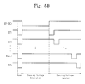
- FIG. 5B is a timing diagram exemplarily showing operating methods of light sensing pixels according to a first embodiment of the present invention
- FIG. 6A is a circuit diagram illustrating a light sensing pixel according to a second embodiment of the present invention.
- FIG. 6B is a timing diagram exemplarily showing operating methods of light sensing pixels according to a second embodiment of the present invention.
- FIG. 7A is a circuit diagram illustrating a light sensing pixel according to a third embodiment of the present invention.
- FIG. 7B is a timing diagram exemplarily showing operating methods of light sensing pixels according to a third embodiment of the present invention.
- FIG. 8A is a circuit diagram illustrating a light sensing pixel according to a fourth embodiment of the present invention.
- FIG. 8B is a timing diagram exemplarily showing operating methods of light sensing pixels according to a fourth embodiment of the present invention.
- FIGS. 9A to 9G are diagrams illustrating an arrangement relationship between a light sensing pixel and a plurality of display pixels in a unit cell according to fifth to eleventh embodiments of the present invention.
- first element is described as being “coupled” or “connected” to a second element, the first element may be directly connected (or directly electrically connected) to the second element, or may be indirectly coupled or electrically coupled to the second element with one or more elements located therebetween.
- a display device according to an embodiment of the present invention will be described below.
- FIG. 1 is a block diagram illustrating a display device according to an embodiment of the present invention.
- a display device includes a timing controller 110 , a display pixel scanner 120 , a display pixel data supplier 130 , a sensing pixel data processor 140 , a sensing pixel driver 150 , and a display panel 200 .
- the display panel 200 may include a plurality of unit cells 210 .
- Each of the unit cells 210 includes display pixels C 1 to C 3 , and a light sensing pixel PS.
- the unit cells 210 may be arranged in a matrix format in a first direction and a second direction perpendicular to the first direction.
- the display panel 200 may include a plurality of gate lines GL 1 to GLn that are extended in the first direction, and a plurality of data lines DL 1 to DLm that are extended in the second direction.
- the second direction may perpendicularly intersect the first direction.
- Each of the display pixels C 1 to C 3 may be coupled to one gate line and one data line.
- the first to third display pixels C 1 to C 3 may include organic light emitting materials for displaying first to third colors, respectively.
- Each of the first to third colors may be any one of red, green, and blue. In other embodiments, each of the first to third colors may be any one of cyan, magenta, and yellow.
- the display panel 200 includes a plurality of sensing voltage generation control lines SC 1 to SCx that are extended in the first direction, and a plurality of sensing voltage transfer control lines ST 1 to STx that are also extended in the first direction.
- the display panel 200 also includes a plurality of sensing data lines SD 1 to SDy that are extended in the second direction.
- the light sensing pixel PS is coupled to one sensing voltage generation control line, one sensing voltage transfer control line, and one sensing data line.
- the light sensing pixels PS included in the unit cells 210 may include an optic-electro converter. Therefore, light inputted to the optic-electro converter may be converted into a sensing voltage.
- the timing controller 110 may generate a scan control signal SCS and a data control signal DCS.
- the timing controller 110 may transfer the scan control signal SCS to the display pixel scanner 120 , and may transfer the data control signal DCS to the display pixel data supplier 130 .
- the timing controller 110 may receive pixel data signals RGB and may transfer the received signals RGB to the display pixel data supplier 130 .
- the display pixel scanner 120 may receive the scan control signal SCS, select one gate line from among the gate lines GL 1 to GLn, and apply a gate voltage to the selected gate line.
- the gate voltage may be applied to the display pixels C 1 to C 3 .
- the display pixel scanner 120 may control timing of the gate voltage that is supplied to the gate lines GL 1 to GLn in response to the scan control signal SCS.
- the display pixel scanner 120 may sequentially apply the gate voltage from the first gate line GL 1 to the nth gate line GLn.
- Switching transistors that are respectively included in display pixels C 1 to C 3 coupled to the selected gate line receiving the gate voltage may be turned on, but switching transistors that are respectively included in display pixels C 1 to C 3 coupled to unselected gate lines receiving no gate voltage, may be turned off.
- Switching transistors that are respectively included in display pixels C 1 to C 3 coupled to the same gate line may be concurrently (e.g., simultaneously) turned on/off.
- the display pixel data supplier 130 may receive the pixel data signals RGB and the data control signal DCS.
- the display pixel data supplier 130 may convert the pixel data signals RGB into analog voltages to supply data output voltages to the data lines DL 1 to DLm.
- the data output voltages may be respectively supplied to the display pixels C 1 to C 3 , which may emit light.
- the sensing pixel driver 150 may transfer signals to the light sensing pixels PS through the sensing voltage transfer control lines ST 1 to STx and the sensing voltage generation control lines SC 1 to SCx, and drive the light sensing pixels PS to generate sensing voltages, respectively.
- the sensing pixel data processor 140 may receive the sensing voltages through the sensing data lines SD 1 to SDy, respectively.
- each of the sensing voltages may include a scanned image data SID.
- the sensing pixel data processor 140 may transfer the scanned image data SID to the outside or the display pixel data supplier 130 .
- At least one of: the display pixel scanner 120 and display pixel data supplier 130 coupled to the display pixels C 1 to C 3 ; or the sensing pixel data processor 140 and sensing pixel driver 150 coupled to the light sensing pixels PS, may be integrated in the display panel. This will be described below with reference to FIGS. 2A and 2B .
- FIGS. 2A and 2B are diagrams illustrating a display device according to a modification example of an embodiment of the present invention.
- the display pixel scanner 120 coupled to the display pixels C 1 to C 3 and the sensing pixel driver 150 coupled to the light sensing pixels PS may be built into the display panel 200 .
- the display pixel scanner 120 and the sensing pixel driver 150 may be mounted on the display panel 200 in a Chip On Glass (COG) type.
- COG Chip On Glass
- the display pixel scanner 120 may be located at one side of the unit cells 210
- the sensing pixel driver 150 may be located at another side of the unit cells 210 .
- the display pixel scanner 120 and the sensing pixel driver 150 may be built into the display panel 200 .
- the display panel 200 may internally include a display pixel and sensing pixel data processor 135 that concurrently (e.g., simultaneously) performs functions of the display pixel data supplier 130 and sensing pixel data processor 140 that have been described above with reference to FIG. 1 .
- the first to third display pixels C 1 to C 3 of the display panel 200 in FIG. 1 may include organic light emitting materials. This will be described below with reference to FIG. 3 .
- FIG. 3 is a circuit diagram exemplarily illustrating the display pixels C 1 to C 3 of the display panel 200 in FIG. 1 .
- FIG. 3 illustrates a display pixel that is coupled to the nth gate line GLn and the mth data line DLm.
- each of the display pixels C 1 to C 3 may include a switching device, a storage device, and a light emitting device.
- the switching device may include the switching transistor 222 and the driving transistor 226 .
- the storage device may be a capacitor 224
- the light emitting device may be an organic light emitting diode OLED.
- Each of the display pixels C 1 to C 3 may display any one of red, green, and blue colors.
- a pixel cell displaying blue, a pixel cell displaying green, and a pixel cell displaying red configure one group, and may be repeatedly arranged in the first and second directions.
- a pixel cell displaying white may be additionally included in the one group.
- the organic light emitting diode OLED may include an anode electrode, a cathode electrode, and an organic emission layer (e.g., an organic phosphor layer) therebetween.
- the organic emission layer may include a Hole Injection Layer (HIL), a Hole Transport Layer (HTL), an Emission Layer (EML), an Electron Transport Layer (ETL), and an Electron Injection Layer (EIL).
- HIL Hole Injection Layer
- HTL Hole Transport Layer
- EML Emission Layer
- ETL Electron Transport Layer
- EIL Electron Injection Layer
- the hole injection layer may be located adjacently to the anode electrode, and the electron injection layer may be located adjacently to the cathode electrode. Holes supplied through the hole injection layer and the hole transport layer recombine with electrons supplied through the electron injection layer and the electron transport layer in the emission layer, and thus the organic light emitting diode OLED may emit light.
- the switching transistor 222 may be turned on by a gate voltage applied through the gate line GLn and transfer a data output voltage applied through the data line DLm to the storage capacitor 224 .
- the storage capacitor 224 may store the data output voltage.
- the driving transistor 226 may be turned on by the data output voltage Dv.
- a driving current may be applied to the organic light emitting diode OLED.
- the driving current is applied to the organic light emitting diode OLED, the organic light emitting diode OLED may emit light.
- the first emission power ELVDD may be a voltage having a level higher than the second emission power ELVSS.
- the first emission power ELVDD may be applied to the anode of the organic light emitting diode OLED, and the second emission power ELVSS may be applied to the cathode of the organic light emitting diode OLED.
- the magnitude of the driving current may be determined by the data output voltage applied to the driving transistor 226 .
- the brightness of the organic light emitting diode OLED may be proportional to the magnitude of the driving current. Accordingly, the brightness of the organic light emitting diode OLED may be determined by the data output voltage.
- the display device may perform the display function and the scan function.
- a scan image may be acquired. This will be described below with reference to FIG. 4A .
- FIG. 4A is a diagram illustrating an operating method of a display device according to an embodiment of the present invention.
- a scanning operation may include first to third emission periods EP 1 to EP 3 , and first to third delivery periods DP 1 to DP 3 .
- the delivery periods DP 1 to DP 3 may be arranged between the emission periods EP 1 to EP 3 .
- a scanning operation may include a first emission period EP 1 , a first delivery period DP 1 , a second emission period EP 2 , a second delivery period DP 2 , a third emission period EP 3 , and a third delivery period DP 3 according to a time order.
- the first display pixels C 1 may emit the first color light.
- the second and third display pixels C 2 and C 3 may not emit lights. Accordingly, the first color light emitted in the first display pixels C 1 may be incident on a scanned object.
- the light sensing pixels PS may be driven and generate first sensing voltages. Specifically, the first color light incident on the scanned object may be reflected by the scanned object. The reflected first color light may be inputted to optic-electro converters included in the light sensing pixels PS, and thus the first sensing voltages may be generated.
- An intensity of the reflected first color light may vary according to the position of the scanned object. For example, as the level of the first color light increases, the intensity of the reflected first color light may become stronger in the scanned object.
- the levels of the first sensing voltages generated in the light sensing pixels PS may be changed according to the intensity of the reflected first color light. Therefore, the first sensing voltages generated in the light sensing pixels PS may include information of the first color of the scanned object.
- the first to third display pixels C 1 to C 3 may not emit light.
- the first sensing voltages may be delivered to the sensing pixel data processor 140 .
- the second display pixels C 2 may emit the second color light, but the first and third display pixels C 1 and C 3 may not emit light. Accordingly, the second color light emitted in the second display pixels C 2 may be reflected by the scanned object. The reflected second color light may be inputted to the optic-electro converters included in the light sensing pixels PS, and thus the second sensing voltages may be generated. The second sensing voltages may include information on the second color of the scanned object.
- the first to third display pixels C 1 to C 3 may not emit light.
- the second sensing voltages may be delivered to the sensing pixel data processor 140 .
- the third display pixels C 3 may emit the third color light, but the first and second display pixels C 1 and C 2 may not emit light. Accordingly, the third color light emitted in the third display pixels C 3 may be reflected by the scanned object. The reflected third color light may be inputted to the optic-electro converters included in the light sensing pixels PS, and thus the third sensing voltages may be generated. The third sensing voltages may include information on the third color of the scanned object.
- the first to third display pixels C 1 to C 3 may not emit light.
- the third sensing voltages may be delivered to the sensing pixel data processor 140 .
- the first to third color sensing voltages may be delivered to the sensing pixel data processor 140 .
- the first to third color sensing voltages may include information of the first to third colors of the scanned object. Therefore, by sequentially scanning the first to third colors of the scanned object, the scanned image data SID of the scanned object may be acquired.
- the scanned image data SID of the scanned object is acquired by sequentially scanning the first to third colors.
- the scanned image data may include information of the first to third colors of the scanned object.
- a scanned object may be scanned in white and black. This will be described below with reference to FIGS. 1 and 4B .
- FIG. 4B is a diagram illustrating an operating method of a display device according to a modified example of an embodiment of the present invention.
- the operating method of the display device may include an emission period EPa and a delivery period DPa.
- the first to third display pixels C 1 to C 3 may emit the first to third color lights concurrently (e.g., simultaneously). Therefore, the display panel 200 may emit white color light.
- the white color light emitted in the first to third display pixels C 1 to C 3 may be incident on a scanned object.
- the light sensing pixels PS may be driven and generate sensing voltages.
- the scanned object may reflect the white color light emitted in the first to third display pixels C 1 to C 3 . Therefore, the sensing voltages generated in the sensing pixels PS may include information on the white-and-black shade of the scanned object. Accordingly, white-and-black scan of the scanned object may be performed.
- the light sensing pixels PS included in the display device according to an embodiment of the present invention may generate and deliver the sensing voltages.
- the light sensing pixels included in the display device according to an embodiment of the present invention and embodiments of an operating method thereof will be described below in detail with reference to FIGS. 5A to 8A and 5 B to 8 B.
- FIGS. 5A to 8A for conciseness, a light sensing pixel coupled to an xth sensing voltage transfer control line STx and a yth sensing data line SDy is illustrated.
- a light sensing pixel and an operating method thereof according to a first embodiment of the present invention will be described below.
- FIG. 5A illustrates the light sensing pixel PS of the display panel 200 that has been described above with reference to FIG. 1 , and is a circuit diagram illustrating a light sensing pixel according to a first embodiment of the present invention.
- a light sensing pixel PS 1 may include a first transistor 232 , a storage capacitor 234 , a second transistor 236 , and an optic-elector converter PV.
- a control terminal of the first transistor 232 may be coupled to the sensing voltage transfer control line STx, an output terminal of the first transistor 232 may be coupled to the sensing data line SDy, and an input terminal of the first transistor 232 may be coupled to a node N 1 .
- a control terminal of the second transistor 236 may be coupled to the sensing voltage generation control line SCx, an input terminal of the second transistor 236 may be coupled to one terminal of the optic-electro converter PV, and an output terminal of the second transistor 236 may be coupled to the node N 1 .
- One electrode of the storage capacitor 234 may be coupled to the node N 1 .
- Another electrode of the capacitor 234 may receive a reference voltage Vr, and another terminal of the optic-electro converter PV may receive a bias voltage Vb.
- FIG. 5B is a timing diagram exemplarily showing operating methods of light sensing pixels according to the first embodiment of the present invention.
- the light sensing pixels PS 1 may perform a reset operation, a sensing voltage generating operation and a sensing voltage transferring operation according to a time order.
- a high-level voltage may be applied to the sensing voltage generation control lines SC 1 to SCx
- a low-level voltage may be applied to the sensing voltage transfer control lines ST 1 to STx
- the first transistors 232 of the light sensing pixels PS 1 may be turned on and the second transistors 236 may be turned off.
- a reset voltage may be applied to the sensing data lines SD 1 to SDy
- the reset voltage may be applied to the node N 1 , and thus the light sensing pixels PS 1 may be reset.
- a low-level voltage may be applied to the sensing voltage generation control lines SC 1 to SCx, and a high-level voltage may be applied to the sensing voltage transfer control lines ST 1 to STx. Accordingly, the first transistors 232 of the light sensing pixels PS 1 may be turned off, and the second transistors 236 may be turned on. Therefore, the sensing voltages generated by the optic-electro converters of the light sensing pixels PS 1 may be transferred to the nodes N 1 , and the storage capacitors 234 may store the sensing voltages.
- a high-level voltage may be applied to the sensing voltage generation control lines SC 1 to SCx, and a low-level voltage may be sequentially applied to the sensing voltage transfer control lines ST 1 to STx in an order from the first sensing voltage transfer control line ST 1 to the xth sensing voltage transfer control line STx. Accordingly, the second transistors 236 of the light sensing pixels PS 1 may be turned off.
- the first transistors 232 of the light sensing pixels PS 1 may be sequentially turned on in an order from the first transistors of the light sensing pixels of a first column coupled to the first sensing voltage transfer control line ST 1 , to the first transistors of the light sensing pixels of an xth column coupled to the xth sensing voltage transfer control line STx. Therefore, from sensing voltages stored in the storage capacitors of the light sensing pixels of the first column to sensing voltages stored in the storage capacitors of the light sensing pixels of the xth column, the sensing voltages may be sequentially transferred to the sensing pixel data processor 140 through the sensing data lines SD 1 to SDy.
- a light sensing pixel and an operating method thereof, according to a second embodiment of the present invention, will be described below.
- FIG. 6A illustrates the light sensing pixel PS of the display panel 200 that has been described above with reference to FIG. 1 , and is a circuit diagram illustrating a light sensing pixel according to the second embodiment of the present invention.
- the sensing voltage generation control lines SC 1 to SCx of FIG. 1 may be omitted.
- a light sensing pixel PS 2 may include a transistor 242 , a storage capacitor 244 , and an optic-elector converter PV.
- a control terminal of the transistor 242 may be coupled to the sensing voltage transfer control line STx, an output terminal of the transistor 242 may be coupled to the sensing data line SDy, and an input terminal of the transistor 242 may be coupled to a node N 2 .
- One end of the optic-electro converter PV and one electrode of the storage capacitor 244 may be coupled to the node N 2 .
- Another electrode of the capacitor 244 may receive a reference voltage Vr, and another terminal of the optic-electro converter PV may receive a bias voltage Vb.
- FIG. 6B is a timing diagram exemplarily showing operating methods of light sensing pixels according to a second embodiment of the present invention.
- the light sensing pixels PS 2 may perform a reset operation, a sensing voltage generating operation, and a sensing voltage transferring operation according to a time order.
- a low-level voltage may be applied to the sensing voltage transfer control lines ST 1 to STx, and thus the transistors 242 of the light sensing pixels PS 2 may be turned on.
- a reset voltage may be applied to the sensing data lines SD 1 to SDy, the reset voltage may be applied to the node N 2 , and thus the light sensing pixels PS 2 may be reset.
- a high-level voltage may be applied to the sensing voltage transfer control lines ST 1 to STx. Accordingly, the transistors 242 of the light sensing pixels PS 2 may be turned off. Therefore, the sensing voltages generated by the optic-electro converters of the light sensing pixels PS 2 may be transferred to the nodes N 2 , and the storage capacitors 244 may store the sensing voltages.
- a low-level voltage may be sequentially applied to the sensing voltage transfer control lines ST 1 to STx in an order from the first sensing voltage transfer control line ST 1 to the xth sensing voltage transfer control line STx.
- the transistors 242 of the light sensing pixels PS 2 may be sequentially turned on in an order from the first transistors of the light sensing pixels of a first column coupled to the first sensing voltage transfer control line ST 1 , to the first transistors of the light sensing pixels of an xth column coupled to the xth sensing voltage transfer control line STx.
- the sensing voltages may be sequentially transferred to the sensing pixel data processor 140 through the sensing data lines SD 1 to SDy.
- a light sensing pixel and an operating method thereof, according to a third embodiment of the present invention, will be described below.
- FIG. 7A illustrates the light sensing pixel PS of the display panel 200 that has been described above with reference to FIG. 1 , and is a circuit diagram illustrating a light sensing pixel according to the third embodiment of the present invention.
- a light sensing pixel PS 3 may include a first transistor 252 , a storage capacitor 254 , a second transistor 256 , and an optic-elector converter PV.
- a control terminal of the first transistor 252 may be coupled to the sensing voltage transfer control line STx, an output terminal of the first transistor 252 may be coupled to the sensing data line SDy, and an input terminal of the first transistor 252 may be coupled to a node N 3 .
- One terminal of the optic-electro converter PV may be coupled to the node N 3 , and another terminal of the optic-electro converter PV may receive a first bias voltage Vb 1 .
- a control terminal of the second transistor 256 may be coupled to the sensing voltage generation control line SCx, an input terminal of the second transistor 256 may be coupled to the one terminal of the optic-electro converter PV, and an output terminal of the second transistor 256 may be coupled to the node N 3 .
- FIG. 7B is a timing diagram exemplarily showing operating methods of light sensing pixels according to a third embodiment of the present invention.
- the light sensing pixels PS 3 may perform a reset operation, a sensing voltage generating operation, and a sensing voltage transferring operation according to a time order.
- a low-level voltage may be applied to the sensing voltage generation control lines SC 1 to SCx
- a high-level voltage may be applied to the sensing voltage transfer control lines ST 1 to STx
- the first transistors 252 of the light sensing pixels PS 3 may be turned off and the second transistors 256 may be turned on. Therefore, a second bias voltage Vb 2 may be transferred to the node N 3 , and thus the light sensing pixels PS 3 may be reset.
- a high-level voltage may be applied to the sensing voltage generation control lines SC 1 to SCx, and a low-level voltage may be applied to the sensing voltage transfer control lines ST 1 to STx. Accordingly, the first and second transistors 252 and 256 of the light sensing pixels PS 3 may be turned off. Therefore, the sensing voltages generated by the optic-electro converters of the light sensing pixels PS 3 may be transferred to the nodes N 3 , and the storage capacitors 254 may store the sensing voltages.
- a high-level voltage may be applied to the sensing voltage generation control lines SC 1 to SCx, and a low-level voltage may be sequentially applied to the sensing voltage transfer control lines ST 1 to STx, in an order from the first sensing voltage transfer control line ST 1 to the xth sensing voltage transfer control line STx. Accordingly, the second transistors 256 of the light sensing pixels PS 3 may be turned off.
- the first transistors 252 of the light sensing pixels PS 3 may be sequentially turned on in an order from the first transistors of the light sensing pixels of a first column connected to the first sensing voltage transfer control line ST 1 , to the first transistors 252 of the light sensing pixels of an xth column coupled to the xth sensing voltage transfer control line STx. Therefore, from sensing voltages stored in the storage capacitors 254 of the light sensing pixels of the first column, to sensing voltages stored in the storage capacitors of the light sensing pixels of the xth column, the sensing voltages may be sequentially transferred to the sensing pixel data processor 140 through the sensing data lines SD 1 to SDy.
- a light sensing pixel and an operating method thereof according to a fourth embodiment of the present invention will be described below.
- FIG. 8A illustrates the light sensing pixel PS of the display panel 200 that has been described above with reference to FIG. 1 , and is a circuit diagram illustrating a light sensing pixel according to the fourth embodiment of the present invention.
- a light sensing pixel PS 4 may include first to third transistors 262 , 264 , and 268 , a storage capacitor 266 , and an optic-elector converter PV.
- a control terminal of the first transistor 262 may be coupled to the sensing voltage transfer control line STx, an output terminal of the first transistor 262 may be coupled to the sensing data line SDy, and an input terminal of the first transistor 262 may be coupled to an output terminal of the second transistor 264 .
- a control terminal of the second transistor 264 may be coupled to a node N 4 , and a reference voltage Vr may be applied to an input terminal of the second transistor 264 .
- One electrode of the storage capacitor 264 may be coupled to the node N 4 , and the reference voltage Vr may be applied to another electrode of the storage capacitor 266 .
- a control terminal of the third transistor 268 may be coupled to the sensing voltage generation control line SCx, an output terminal of the third transistor 268 may be coupled to one terminal of the optic-electro converter PV, and an input terminal of the third transistor 268 may be coupled to the node N 4 .
- a bias voltage Vb 3 may be applied to another terminal of the optic-electro converter PV.
- FIG. 8B is a timing diagram exemplarily showing operating methods of light sensing pixels according to the fourth embodiment of the present invention.
- the light sensing pixels PS 4 may perform a reset operation, a sensing voltage generating operation, and a sensing voltage transferring operation according to a time order.
- a low-level voltage may be applied to the sensing voltage generation control lines SC 1 to SCx
- a high-level voltage may be applied to the sensing voltage transfer control lines ST 1 to STx
- the bias voltage Vb 3 may have a high level.
- the first transistors 262 of the light sensing pixels PS 4 may be turned off, and the third transistors 268 may be turned on.
- the optic-electro converter PV includes a PN diode
- a forward current flows in the optic-electro converter PV when the bias voltage Vb 3 has a high level, and the bias voltage Vb 3 may be transferred to the node N 4 . Accordingly the light sensing pixels PS 4 may be reset.
- a low-level voltage may be applied to the sensing voltage generation control lines SC 1 to SCx, and a high-level voltage may be applied to the sensing voltage transfer control lines ST 1 to STx. Accordingly, the first transistors 262 of the light sensing pixels PS 4 may be turned off, and the third transistors 268 may be turned on. Therefore, the sensing voltages generated by the optic-electro converters of the light sensing pixels PS 4 may be transferred to the nodes N 4 , and the storage capacitors 266 may store the sensing voltages.
- the second transistors 264 may be turned on by the sensing voltages transferred to the nodes N 4 .
- the second transistors 264 may transfer total or a portion of the reference voltage Vr to the input terminals of the first transistors 262 according to levels of the sensing voltages.
- a high-level voltage may be applied to the sensing voltage generation control lines SC 1 to SCx, and a low-level voltage may be sequentially applied to the sensing voltage transfer control lines ST 1 to STx in an order from the first sensing voltage transfer control line ST 1 , to the xth sensing voltage transfer control line STx. Accordingly, the third transistors 268 of the light sensing pixels PS 4 may be turned off.
- the first transistors 262 of the light sensing pixels PS 4 may be sequentially turned on in an order from the first transistors of the light sensing pixels of a first column coupled to the first sensing voltage transfer control line ST 1 , to the first transistors of the light sensing pixels of an xth column coupled to the xth sensing voltage transfer control line STx. Therefore, from sensing voltages stored in the storage capacitors of the light sensing pixels of the first column to sensing voltages stored in the storage capacitors of the light sensing pixels of the xth column, the sensing voltages may be sequentially transferred to the sensing pixel data processor 140 through the sensing data lines SD 1 to SDy.
- the display device may include the plurality of display pixels C 1 to C 3 , and the plurality of unit cell 210 respectively including one light sensing pixel PS.
- An arrangement relationship between the light sensing pixel PS and the display pixels C 1 to C 3 of the unit cell 210 included in the display panel 200 of FIG. 1 will be described below with reference to FIGS. 9A to 9G .
- FIGS. 9A to 9G are for describing the unit cell of the display panel that has been described above with reference to FIG. 1 , and are diagrams illustrating an arrangement relationship between a light sensing pixel and a plurality of display pixels in a unit cell according to fifth to eleventh embodiments of the present invention.
- a unit cell 210 a may include one light sensing pixel PS and a plurality of display pixels C 1 to C 3 .
- the light sensing pixel PS may be extended in a first direction. In a plan view, the light sensing pixel PS has a long side in a first direction.
- a plurality of first display pixels C 1 may be arranged sequentially along the first direction.
- a plurality of second display pixels C 2 may be arranged sequentially along the first direction.
- a plurality of third display pixels C 3 may be arranged sequentially along the first direction.
- the plurality of first to third display pixels C 1 to C 3 in the unit cell 210 a may configure a display pixel group.
- the display pixel group may be located at one side of the light sensing pixel PS.
- a unit cell 210 b may include a light sensing pixel PS extended in the first direction, and a display pixel group. Unlike the embodiment shown in FIG. 9A , the display pixel group may be provided in plurality. The display pixel groups may be located at both sides of the light sensing pixel PS.
- a unit cell 210 c may include one light sensing pixel PS and a plurality of display pixels C 1 to C 3 .
- the light sensing pixel PS may be extended in a second direction. In a plan view, the light sensing pixel PS has a long side in the second direction.
- the plurality of first display pixels C 1 may be sequentially arranged along the second direction.
- the plurality of second display pixels C 2 may be sequentially arranged along the second direction.
- the plurality of third display pixels C 3 may be sequentially arranged along the second direction.
- the plurality of first to third display pixels C 1 to C 3 in the unit cell 210 c may configure a display pixel group.
- the display pixel group may be located at one side of the light sensing pixel PS.
- a unit cell 210 d may include a light sensing pixel PS extended in the second direction, and a display pixel group. Unlike the embodiment illustrated in FIG. 9C , the display pixel group may be provided in plurality. The display pixel groups may be located at both sides of the light sensing pixel PS.
- a unit cell 210 e may include one light sensing pixel PS and first to third display pixels C 1 to C 3 .
- the third display pixel C 3 may be larger than the first and second display pixels C 1 and C 2 .
- the third display pixel C 3 may include an organic light emitting material for displaying blue.
- a unit cell 210 f may include one light sensing pixel PS, a first display pixel C 1 , a second display pixel C 2 , and a third display pixel C 3 that is larger than the first and second display pixels C 1 and C 2 .
- the unit cell 210 f may include a plurality of the first display pixels C 1 , a plurality of the second display pixels C 2 , and a plurality of the third display pixels C 3 .
- a unit cell 210 g may include one light sensing pixel PS, a plurality of first display pixels C 1 , a plurality of second display pixels C 2 , and a plurality of third display pixels C 3 .
- the size of the third display pixel C 3 may be larger than the sizes of the first and second display pixels C 1 and C 2 .
- the third display pixels C 3 may include an organic light emitting material for displaying blue.
- the first to third display pixels C 1 to C 3 may surround the periphery of the light sensing pixel PS. Therefore, the light sensing pixel PS may be surrounded by the first to third display pixels C 1 to C 3 .
- the first to third display pixels that respectively include the organic light emitting materials for displaying the first to third colors, and the display panel that includes the plurality of unit cells including the one light sensing pixel. Therefore, provided is the display device that performs the display function and the scan function concurrently (e.g., simultaneously), and has a high aperture ratio and high reliability.
Abstract
Description
Claims (19)
Applications Claiming Priority (2)
| Application Number | Priority Date | Filing Date | Title |
|---|---|---|---|
| KR10-2011-0012558 | 2011-02-11 | ||
| KR1020110012558A KR20120092471A (en) | 2011-02-11 | 2011-02-11 | Display device and method of operating the same |
Publications (2)
| Publication Number | Publication Date |
|---|---|
| US20120206049A1 US20120206049A1 (en) | 2012-08-16 |
| US8994618B2 true US8994618B2 (en) | 2015-03-31 |
Family
ID=46636362
Family Applications (1)
| Application Number | Title | Priority Date | Filing Date |
|---|---|---|---|
| US13/177,374 Active 2033-01-17 US8994618B2 (en) | 2011-02-11 | 2011-07-06 | Display device and operating method thereof |
Country Status (2)
| Country | Link |
|---|---|
| US (1) | US8994618B2 (en) |
| KR (1) | KR20120092471A (en) |
Families Citing this family (3)
| Publication number | Priority date | Publication date | Assignee | Title |
|---|---|---|---|---|
| CN104051672B (en) * | 2014-07-09 | 2019-01-01 | 深圳市华星光电技术有限公司 | OLED pixel structure |
| WO2021250507A1 (en) * | 2020-06-12 | 2021-12-16 | 株式会社半導体エネルギー研究所 | Drive method for display device |
| CN113363270B (en) * | 2021-05-28 | 2023-05-09 | 深圳市华星光电半导体显示技术有限公司 | Pixel arrangement structure and display panel |
Citations (9)
| Publication number | Priority date | Publication date | Assignee | Title |
|---|---|---|---|---|
| JPH10150525A (en) | 1996-06-10 | 1998-06-02 | Internatl Business Mach Corp <Ibm> | System for optically scanning image by using optical shutter |
| US20070109239A1 (en) * | 2005-11-14 | 2007-05-17 | Den Boer Willem | Integrated light sensitive liquid crystal display |
| US20080158120A1 (en) * | 2006-12-29 | 2008-07-03 | Lg.Philips Lcd Co., Ltd. | Liquid crystal display device including image sensor and method of driving the same |
| US20080191979A1 (en) * | 2005-02-18 | 2008-08-14 | Masao Nakane | Display Control Device and Display Device |
| KR20080096131A (en) | 2007-04-27 | 2008-10-30 | 엘지디스플레이 주식회사 | Field sequential color driving method of lcd device with built-in image sensor |
| US20090002336A1 (en) * | 2007-03-02 | 2009-01-01 | Jin-Young Choi | Display device including integrated touch sensors |
| KR20090058888A (en) | 2007-12-05 | 2009-06-10 | 엘지디스플레이 주식회사 | Liquid crystal display device for image scanner |
| KR20090124340A (en) | 2008-05-29 | 2009-12-03 | 엘지디스플레이 주식회사 | Scanning apparatus of notebook computer |
| US20100156780A1 (en) * | 1998-07-08 | 2010-06-24 | E Ink Corporation | Methods for achieving improved color in microencapsulated electrophoretic devices |
-
2011
- 2011-02-11 KR KR1020110012558A patent/KR20120092471A/en not_active Application Discontinuation
- 2011-07-06 US US13/177,374 patent/US8994618B2/en active Active
Patent Citations (10)
| Publication number | Priority date | Publication date | Assignee | Title |
|---|---|---|---|---|
| JPH10150525A (en) | 1996-06-10 | 1998-06-02 | Internatl Business Mach Corp <Ibm> | System for optically scanning image by using optical shutter |
| US6005990A (en) | 1996-06-10 | 1999-12-21 | International Business Machines Corporation | System for optically scanning images using optical shutter |
| US20100156780A1 (en) * | 1998-07-08 | 2010-06-24 | E Ink Corporation | Methods for achieving improved color in microencapsulated electrophoretic devices |
| US20080191979A1 (en) * | 2005-02-18 | 2008-08-14 | Masao Nakane | Display Control Device and Display Device |
| US20070109239A1 (en) * | 2005-11-14 | 2007-05-17 | Den Boer Willem | Integrated light sensitive liquid crystal display |
| US20080158120A1 (en) * | 2006-12-29 | 2008-07-03 | Lg.Philips Lcd Co., Ltd. | Liquid crystal display device including image sensor and method of driving the same |
| US20090002336A1 (en) * | 2007-03-02 | 2009-01-01 | Jin-Young Choi | Display device including integrated touch sensors |
| KR20080096131A (en) | 2007-04-27 | 2008-10-30 | 엘지디스플레이 주식회사 | Field sequential color driving method of lcd device with built-in image sensor |
| KR20090058888A (en) | 2007-12-05 | 2009-06-10 | 엘지디스플레이 주식회사 | Liquid crystal display device for image scanner |
| KR20090124340A (en) | 2008-05-29 | 2009-12-03 | 엘지디스플레이 주식회사 | Scanning apparatus of notebook computer |
Also Published As
| Publication number | Publication date |
|---|---|
| KR20120092471A (en) | 2012-08-21 |
| US20120206049A1 (en) | 2012-08-16 |
Similar Documents
| Publication | Publication Date | Title |
|---|---|---|
| US11790837B2 (en) | Pixel and display apparatus including same | |
| US8111219B2 (en) | Pixel, organic light emitting display using the same, and associated methods | |
| JP5616110B2 (en) | Organic electroluminescence display | |
| US8416157B2 (en) | Organic light emitting display and driving circuit thereof | |
| US20080158114A1 (en) | Organic electroluminescent display device and method of driving the same | |
| US9583042B2 (en) | Display device having a power providing line | |
| US20110025678A1 (en) | Organic light emitting display device and driving method thereof | |
| CN111968569B (en) | Pixel circuit, array substrate, driving method of array substrate and display panel | |
| US20100201673A1 (en) | Light emitting display device and method of driving the same | |
| US20080211744A1 (en) | Organic light emitting display and driving circuit thereof | |
| CN101859529A (en) | Display device and the driving method that is used for display device | |
| US7315293B2 (en) | Organic light-emitting diode display device | |
| US10621912B2 (en) | Display device to display images on rear and front surfaces independently of each other | |
| US8994618B2 (en) | Display device and operating method thereof | |
| US20100220088A1 (en) | Power supply unit and organic light emitting display device using the same | |
| US8610448B2 (en) | One-sheet test device and test method thereof | |
| JP3879281B2 (en) | Display device and driving method of display device | |
| KR100941591B1 (en) | Stacked active matrix organic light emitting diode, Stacked active matrix organic light emitting diode array arranging the same and Driving method thereof | |
| JP2005338824A (en) | Electroluminescent display and pixel driving unit thereof | |
| JP5867989B2 (en) | Display device | |
| US20240062723A1 (en) | Display device | |
| US11367384B2 (en) | Display device capable of improving power consumption and method for driving the same | |
| US11915656B2 (en) | Gate driver and display device including the same | |
| US20220165212A1 (en) | Pixel circuit, driving method thereof and display device | |
| US11468828B2 (en) | Electroluminescent display panel having pixel driving circuit |
Legal Events
| Date | Code | Title | Description |
|---|---|---|---|
| AS | Assignment |
Owner name: SAMSUNG MOBILE DISPLAY CO., LTD., KOREA, REPUBLIC Free format text: ASSIGNMENT OF ASSIGNORS INTEREST;ASSIGNORS:HAN, SANGMYEON;PARK, JONGHWA;REEL/FRAME:026557/0212 Effective date: 20110614 |
|
| AS | Assignment |
Owner name: SAMSUNG DISPLAY CO., LTD., KOREA, REPUBLIC OF Free format text: MERGER;ASSIGNOR:SAMSUNG MOBILE DISPLAY CO., LTD.;REEL/FRAME:028769/0551 Effective date: 20120702 |
|
| FEPP | Fee payment procedure |
Free format text: PAYOR NUMBER ASSIGNED (ORIGINAL EVENT CODE: ASPN); ENTITY STATUS OF PATENT OWNER: LARGE ENTITY |
|
| STCF | Information on status: patent grant |
Free format text: PATENTED CASE |
|
| MAFP | Maintenance fee payment |
Free format text: PAYMENT OF MAINTENANCE FEE, 4TH YEAR, LARGE ENTITY (ORIGINAL EVENT CODE: M1551); ENTITY STATUS OF PATENT OWNER: LARGE ENTITY Year of fee payment: 4 |
|
| MAFP | Maintenance fee payment |
Free format text: PAYMENT OF MAINTENANCE FEE, 8TH YEAR, LARGE ENTITY (ORIGINAL EVENT CODE: M1552); ENTITY STATUS OF PATENT OWNER: LARGE ENTITY Year of fee payment: 8 |