US8988566B2 - Lens array for partitioned image sensor having color filters - Google Patents

Lens array for partitioned image sensor having color filters Download PDF

Info

Publication number
US8988566B2
US8988566B2 US13/570,449 US201213570449A US8988566B2 US 8988566 B2 US8988566 B2 US 8988566B2 US 201213570449 A US201213570449 A US 201213570449A US 8988566 B2 US8988566 B2 US 8988566B2
Authority
US
United States
Prior art keywords
lens
focal length
image sensor
curvature
color filter
Prior art date
Legal status (The legal status is an assumption and is not a legal conclusion. Google has not performed a legal analysis and makes no representation as to the accuracy of the status listed.)
Active, expires
Application number
US13/570,449
Other versions
US20140043507A1 (en
Inventor
Chia-Ching Wang
Jau-Jan Deng
Yun-Chiang Hsu
Current Assignee (The listed assignees may be inaccurate. Google has not performed a legal analysis and makes no representation or warranty as to the accuracy of the list.)
Omnivision Technologies Inc
Original Assignee
Omnivision Technologies Inc
Priority date (The priority date is an assumption and is not a legal conclusion. Google has not performed a legal analysis and makes no representation as to the accuracy of the date listed.)
Filing date
Publication date
Application filed by Omnivision Technologies Inc filed Critical Omnivision Technologies Inc
Priority to US13/570,449 priority Critical patent/US8988566B2/en
Assigned to OMNIVISION TECHNOLOGIES, INC. reassignment OMNIVISION TECHNOLOGIES, INC. ASSIGNMENT OF ASSIGNORS INTEREST (SEE DOCUMENT FOR DETAILS). Assignors: DENG, JAU-JAN, HSU, YUN-CHIANG, WANG, CHIA-CHING
Priority to TW102124070A priority patent/TWI549273B/en
Priority to CN201310313751.4A priority patent/CN103579268B/en
Priority to EP13179183.2A priority patent/EP2696570B1/en
Publication of US20140043507A1 publication Critical patent/US20140043507A1/en
Application granted granted Critical
Publication of US8988566B2 publication Critical patent/US8988566B2/en
Active legal-status Critical Current
Adjusted expiration legal-status Critical

Links

Images

Classifications

    • H04N5/2254
    • HELECTRICITY
    • H01ELECTRIC ELEMENTS
    • H01LSEMICONDUCTOR DEVICES NOT COVERED BY CLASS H10
    • H01L27/00Devices consisting of a plurality of semiconductor or other solid-state components formed in or on a common substrate
    • H01L27/14Devices consisting of a plurality of semiconductor or other solid-state components formed in or on a common substrate including semiconductor components sensitive to infrared radiation, light, electromagnetic radiation of shorter wavelength or corpuscular radiation and specially adapted either for the conversion of the energy of such radiation into electrical energy or for the control of electrical energy by such radiation
    • H01L27/144Devices controlled by radiation
    • H01L27/146Imager structures
    • H01L27/14601Structural or functional details thereof
    • H01L27/1462Coatings
    • H01L27/14621Colour filter arrangements
    • HELECTRICITY
    • H04ELECTRIC COMMUNICATION TECHNIQUE
    • H04NPICTORIAL COMMUNICATION, e.g. TELEVISION
    • H04N23/00Cameras or camera modules comprising electronic image sensors; Control thereof
    • H04N23/50Constructional details
    • H04N23/55Optical parts specially adapted for electronic image sensors; Mounting thereof
    • HELECTRICITY
    • H01ELECTRIC ELEMENTS
    • H01LSEMICONDUCTOR DEVICES NOT COVERED BY CLASS H10
    • H01L27/00Devices consisting of a plurality of semiconductor or other solid-state components formed in or on a common substrate
    • H01L27/14Devices consisting of a plurality of semiconductor or other solid-state components formed in or on a common substrate including semiconductor components sensitive to infrared radiation, light, electromagnetic radiation of shorter wavelength or corpuscular radiation and specially adapted either for the conversion of the energy of such radiation into electrical energy or for the control of electrical energy by such radiation
    • H01L27/144Devices controlled by radiation
    • H01L27/146Imager structures
    • H01L27/14601Structural or functional details thereof
    • H01L27/14625Optical elements or arrangements associated with the device
    • H01L27/14627Microlenses
    • HELECTRICITY
    • H01ELECTRIC ELEMENTS
    • H01LSEMICONDUCTOR DEVICES NOT COVERED BY CLASS H10
    • H01L27/00Devices consisting of a plurality of semiconductor or other solid-state components formed in or on a common substrate
    • H01L27/14Devices consisting of a plurality of semiconductor or other solid-state components formed in or on a common substrate including semiconductor components sensitive to infrared radiation, light, electromagnetic radiation of shorter wavelength or corpuscular radiation and specially adapted either for the conversion of the energy of such radiation into electrical energy or for the control of electrical energy by such radiation
    • H01L27/144Devices controlled by radiation
    • H01L27/146Imager structures
    • H01L27/14601Structural or functional details thereof
    • H01L27/14632Wafer-level processed structures
    • HELECTRICITY
    • H04ELECTRIC COMMUNICATION TECHNIQUE
    • H04NPICTORIAL COMMUNICATION, e.g. TELEVISION
    • H04N25/00Circuitry of solid-state image sensors [SSIS]; Control thereof
    • H04N25/10Circuitry of solid-state image sensors [SSIS]; Control thereof for transforming different wavelengths into image signals
    • H04N25/11Arrangement of colour filter arrays [CFA]; Filter mosaics
    • H04N25/13Arrangement of colour filter arrays [CFA]; Filter mosaics characterised by the spectral characteristics of the filter elements
    • H04N25/134Arrangement of colour filter arrays [CFA]; Filter mosaics characterised by the spectral characteristics of the filter elements based on three different wavelength filter elements
    • H04N9/045
    • HELECTRICITY
    • H01ELECTRIC ELEMENTS
    • H01LSEMICONDUCTOR DEVICES NOT COVERED BY CLASS H10
    • H01L27/00Devices consisting of a plurality of semiconductor or other solid-state components formed in or on a common substrate
    • H01L27/14Devices consisting of a plurality of semiconductor or other solid-state components formed in or on a common substrate including semiconductor components sensitive to infrared radiation, light, electromagnetic radiation of shorter wavelength or corpuscular radiation and specially adapted either for the conversion of the energy of such radiation into electrical energy or for the control of electrical energy by such radiation
    • H01L27/144Devices controlled by radiation
    • H01L27/146Imager structures
    • H01L27/14683Processes or apparatus peculiar to the manufacture or treatment of these devices or parts thereof
    • H01L27/14685Process for coatings or optical elements

Definitions

  • the present invention relates generally to image sensors, and more specifically, to a lens array for a partitioned image sensor having color filters.
  • An image capture unit typically includes an image sensor and an imaging lens.
  • the imaging lens focuses light onto the image sensor to form an image, and the image sensor converts the light into electric signals.
  • the electric signals are output from the image capture unit to other units in a host electronic system or a subsystem.
  • the electronic system may be a mobile phone, a computer, a digital camera or a medical device.
  • image capture units are increasingly required to have lower profiles so that overall sizes of electronic systems including the image capture units can be reduced while at the same time not sacrifice quality in the optical images that are captured.
  • the profile of an image capture unit may be associated with the distance from the bottom of image sensor to the top of the imaging lens.
  • FIG. 1A is a schematic diagram of an image capture unit including an imaging lens and an image sensor.
  • FIG. 1B is a schematic diagram of a low profile image capture unit including a low profile imaging lens and an image sensor.
  • FIG. 2 illustrates one example of an image sensor having four partitioned areas in accordance with the teachings of the present invention.
  • FIG. 3A is a cross-section illustrating two lenses having different focal lengths and two partitioned areas of one example of a low profile image capture unit in accordance with the teachings of the present invention.
  • FIG. 3B is a cross-section illustrating two lenses having different radii of curvature and two partitioned areas of one example of a low profile image capture unit in accordance with the teachings of the present invention.
  • FIG. 4 illustrates example transmission spectra of photo-resist materials for red, green, and blue filters.
  • FIG. 5 illustrates one example of a 2 ⁇ 2 lens array for a partitioned image sensor in accordance with the teachings of the present invention.
  • FIG. 6 illustrates one example of a 2 ⁇ 2 lens array on a partitioned image sensor in accordance with the teachings of the present invention.
  • FIG. 7A illustrates a cross section of one example of a 2 ⁇ 2 lens array on a partitioned image sensor in accordance with the teachings of the present invention.
  • FIG. 7B illustrates another cross section of one example of a 2 ⁇ 2 lens array on a partitioned image sensor in accordance with the teachings of the present invention.
  • FIG. 8A illustrates an example combined transmission spectrum of an IR-cut filter and red color filter in accordance with the teachings of the present invention.
  • FIG. 8B illustrates an example transmission spectrum of a green color filter in accordance with the teachings of the present invention.
  • FIG. 8C illustrates an example transmission spectrum of blue color filter in accordance with the teachings of the present invention.
  • FIG. 8D illustrates an example daylight spectrum transmitted through a UV-IR-cut filter in accordance with the teachings of the present invention.
  • FIG. 8E illustrates an example transmission spectra of UV-IR-cut filter for 0°, 25°, 30°, and 35° incident light in accordance with the teachings of the present invention.
  • FIG. 9 illustrates example transmission spectra of multilayer dielectric coatings red, green, and blue bandpass filters in accordance with the teachings of the present invention.
  • FIG. 10 illustrates the cross section of a lens cube of a lens array on a partitioned image sensor in accordance with the teachings of the present invention.
  • FIG. 11 is a block diagram illustrating one example of an image sensor in accordance with the teachings of the present invention.
  • a low profile image capture unit may include an array of lenses having individual filters disposed on a partitioned image sensor.
  • the quality of optical images captured which may for example be express in terms of resolution (i.e., the number of pixels) and/or sharpness, is not sacrificed for the low profile in accordance with the teachings of the present invention.
  • FIG. 1A is a schematic diagram of an image capture unit 200 including an imaging lens 202 and an image sensor 204 .
  • the distance between lens 202 and image sensor 204 is approximately f, where f is the focal length of lens 202 .
  • the width of the image sensor 204 covered by lens 202 is W, and the lens diameter is D.
  • FIG. 1B shows a schematic diagram of a low profile image capture unit 210 including an imaging lens 212 and an image sensor 214 .
  • the distance between lens 212 and image sensor 214 is approximately f/2, where f/2 is the focal length of lens 212 .
  • the width of the image sensor 214 covered by lens 212 is W/2, and the lens diameter is D/2.
  • Image sensors 204 and 214 are the same image sensor, and both image sensors have the same pixel array structure. Since the width of image sensor 214 is half of the width of image sensor 204 , image sensor 214 will have half of number of pixels as compared with image sensor 204 in one dimension. In two dimensions, image sensor 214 will have quarter of number of pixels as compared with image sensor 204 . In other words, the number of pixels of the image captured is approximately proportional to the square of the scale of the distance between the lens and the image sensor.
  • FIG. 2 illustrates an image sensor 220 having four partitioned areas 222 , 224 , 226 , and 228 closely arranged proximate to each other in accordance with the teachings of the present invention.
  • Each partitioned area 222 , 224 , 226 , and 228 is covered by a respective imaging lens (e.g., lens 212 of FIG. 1B ).
  • the focal length of the imaging lens e.g., lens 212 of FIG. 1B
  • the focal length of the imaging lens can be half of the imaging lens when the image sensor is not partitioned into four areas (e.g., lens 202 of FIG. 1A ).
  • a low profile image capture unit can be constructed using four lenses and four partitioned areas of an image sensor.
  • the low profile image capture unit will have approximately the same resolution (i.e., the same number of pixels) as compared with the original image capture unit, because four areas of image sensor are used.
  • An area of image sensor may be similar to image sensor 214 of FIG
  • FIG. 3A shows a cross-section of low profile image capture unit 300 including four imaging lenses and four partitioned areas of image sensor in accordance with the teachings of the present invention.
  • the cross-section illustrated in FIG. 3A may correspond with dashed line A-A′ of FIG. 2 .
  • the four partitioned areas of image sensor may be areas 222 , 224 , 226 , and 228 of image sensor 220 of FIG. 2 .
  • FIG. 3A Only two partitioned areas 222 and 224 of image sensor 220 are shown in FIG. 3A .
  • an image capture system having low profile can be constructed, while the resolution (i.e., the number of pixels) of images captured can be maintained.
  • imaging lens 302 is positioned a first focal length f 1 away from respective image sensor 222 .
  • Imaging lens 304 is positioned a second focal length f 2 away from respective image sensor 224 .
  • the second focal length f 2 is approximately half of the focal length when compared with lens 202 shown in FIG. 1A .
  • example image capture unit 300 of FIG. 3A is a low profile image capture unit such that the width of the image sensors 222 and 224 covered by lens 302 and 304 are W/2, and the lens diameters of lenses 302 and 304 are D/2 in accordance with the teachings of the present invention.
  • a typical image capture unit may include a Bayer type color filter array on the image sensor.
  • Bayer type color filter array is typically made from photo-resist materials.
  • the transmission spectra of photo-resist materials for red (R), green (G), and blue (B) filters are depicted in FIG. 4 .
  • the transmission of red filter includes an IR spectrum, e.g., wavelength beyond 650 nm.
  • an IR-cut filter is generally required to cut the transmission of wavelength beyond 650 nm.
  • crosstalk domains in FIG. 4 that may degrade the quality of the color image.
  • partitioned areas of image sensor 222 and 224 of FIG. 3A may not include Bayer type color filter array.
  • partitioned areas 222 , 224 , 226 , and 228 may be designated to red (R), green (G), clear (C), and blue (B) areas, respectively.
  • Red area may be covered by a single red filter
  • green area may be covered by a single green filter
  • blue area may be covered by a single blue filter
  • clear or C area may not be covered by any filter or may be covered by a single green filter.
  • Bayer type color filter array on the image sensor is based on a semiconductor lithographic process requiring very accurate overlay as sensor pitch decreases.
  • the Bayer type color filter coating is a very expensive process.
  • rework process will increase risk of damaging the image sensor.
  • the single color filter coating on a glass substrate e.g., a glass wafer of a wafer-level lens cube, is an inexpensive process without necessity of accurate mask and alignment. Rework on glass substrate is very easy.
  • the first focal length f 1 may be different than the second focal length f 2 .
  • the first focal length f 1 corresponds with light having a first color, such as for example but not limited to red (R)
  • second focal length f 2 corresponds with light having a second color, such as for example but not limited to green (G).
  • R red
  • G green
  • a single image having the first color is focused by lens 302 onto image sensor 222 and the same single image having the second color is focused by lens 304 onto image sensor 224 in accordance with the teachings of the present invention.
  • the red (R) area includes red pixels only
  • the green (G) area includes green pixels only
  • the blue (B) area includes blue pixels only.
  • the clear or C area may include white pixels when no filter is applied, and green pixels when a green filter is applied.
  • a readout system and/or processor may rearrange red, green, and blue pixels into Bayer pattern or any pattern for further processing the color signals and forming the color images.
  • C pixels may be use as white pixels for particular processing or simply contribute as green pixels in accordance with the teachings of the present invention.
  • FIG. 5 illustrates a lens array 400 for the partitioned image sensor in accordance with the teachings of the present invention.
  • the partitioned image sensor may be image sensor 220 of FIG. 2 .
  • Lens array 400 may be a 2 ⁇ 2 array having low profile lenses 402 , 404 , 406 , and 408 , which are designated to red (R), green (G), clear (C), and blue (B) areas, respectively.
  • each one of the lenses 402 , 404 , 406 , and 408 is arranged to focus a single image onto a respective one of the red (R), green (G), clear (C), and blue (B) areas image sensor regions.
  • lens 402 forms a red image only
  • lens 404 forms a green image only
  • lens 408 forms a blue image only.
  • each one of the lenses 402 , 404 , 406 , and 408 has a different respective focal length that corresponds with the specific color of light that is being focused onto the corresponding image sensor region (e.g., see FIG. 3A ).
  • each one of the lenses 402 , 404 , 406 , and 408 has a different respective radius of curvature (ROC) that corresponds with the specific color of light that is being focused onto the corresponding image sensor region (e.g., see FIG. 3B ).
  • lenses 402 , 404 , 406 , and 408 may have the same focal length and the same ROC.
  • FIG. 3B shows a cross-section of low profile image capture unit 320 including four imaging lenses and four partitioned areas of image sensor in accordance with the teachings of the present invention.
  • the cross-section illustrated in FIG. 3B may correspond with dashed line A-A′ of FIG. 2 .
  • the ROC of lenses 402 and 404 are different such that the focal lengths of lenses 402 and 404 become the same.
  • each lens 402 , 404 , 406 , and 408 at individual color may be the same, and thus no individual adjustment of the focal length distance between each lens and the corresponding image sensor is necessary, in accordance with the teachings of the present invention. While the radii of curvature of R, G, and B lenses are different, the ROC of C lens 406 may be the same with one of lenses 402 , 404 , and 408 .
  • lenses 402 , 404 , 406 , and 408 may have the same ROC, and the focal length difference of lenses 402 , 404 , 406 , and 408 may be small and negligible, in accordance with the teachings of the present invention (e.g., see FIGS. 7A and 7B ).
  • FIG. 7A illustrates an example including the cross-section 550 of 2 ⁇ 2 lens array 500 in accordance with the teachings of the present invention. Only lens cubes 502 and 504 are shown in FIG. 7A .
  • the cross-section illustrated in FIG. 7A may correspond with dashed line B-B′ of FIG. 6 .
  • lens cubes 502 and 504 are disposed on a cover glass 510 .
  • Partitioned areas 512 and 514 of a single image sensor are under cover glass 510 , aligned with lens cubes 502 and 504 , respectively.
  • each wafer-level lens cube includes at least a glass wafer and a lens on the glass wafer.
  • each wafer-level lens cube may include a lens 520 on a glass wafer 522 , a lens 524 on the other side of glass wafer 522 , a lens 528 on a glass wafer 530 , a lens 532 on the other side of glass wafer 530 , glass wafers 522 and 530 , a spacer 526 between glass wafers 522 and 530 , and a spacer 518 between glass wafer 530 and cover glass 510 .
  • an IR-cut filter 702 is disposed on a glass wafer 562 underneath a lens 560 .
  • IR-cut filter 702 may be multilayer dielectric coatings.
  • the multilayer dielectric coatings may include alternate layers of high and low refractive indexes.
  • a red color filter 704 is disposed in contact with the other side of glass wafer 562 between glass wafer 562 and a lens 564 .
  • Red color filter 704 may be a photo-resist coating.
  • the combined transmission spectrum of IR-cut filter 702 and red color filter 704 is depicted in FIG. 8A . In one example, the transmission of wavelengths beyond 650 nm will be cut by IR-cut filter 702 .
  • Green color filter 706 is disposed in contact with glass wafer 522 between glass wafer 522 and lens 524 .
  • Green color filter 706 may be a photo-resist coating.
  • the transmission spectrum of green color filter 706 is depicted in FIG. 8B .
  • IR-cut filter 702 and red filter 704 may be formed on either side of glass wafer 562 . Furthermore, IR-cut filter 702 and red filter 704 may be formed on either side of a second glass wafer 566 . Similarly, green filter 706 may be formed on either side of glass wafer 522 , or either side of second glass wafer 530 , in accordance with the teachings of the present invention.
  • FIG. 7B illustrates the cross-section 600 of 2 ⁇ 2 lens array 500 in accordance with the teachings of the present invention. Only lens cubes 506 and 508 are shown in FIG. 7B .
  • the cross-section illustrated in FIG. 7B may correspond with dashed line C-C′ of FIG. 6 .
  • lens cubes 506 and 508 are disposed on a cover glass 510 .
  • Partitioned areas 612 and 614 of a single image sensor are under cover glass 510 , aligned with lens cubes 506 and 508 , respectively.
  • a blue color filter 708 is disposed in contact with a glass wafer 662 between glass wafer 662 and a lens 664 .
  • Blue color filter 708 may be a photo-resist coating.
  • the transmission spectrum of blue color filter 708 is depicted in FIG. 8C .
  • a UV-IR-cut filter 710 is disposed on a glass wafer 622 underneath a lens 620 .
  • UV-IR-cut filter 710 may be multilayer dielectric coatings.
  • the multilayer dielectric coatings may include 30 alternate layers of high and low refractive indexes.
  • the daylight spectrum transmitted through UV-IR-cut filter 710 is depicted in FIG. 8D .
  • UV-IR-cut filter 710 The transmission spectra of UV-IR-cut filter 710 for 0°, 25°, 30°, and 35° incident light are depicted in FIG. 8E .
  • UV-IR-cut filter cuts the transmissions of wavelengths longer than 650 nm and shorter than 420 nm.
  • Blue filter 708 may be formed on either side of glass wafer 662 , or either side of a second glass wafer 666 .
  • UV-IR-cut filter 710 may be formed on either side of glass wafer 622 , or either side of a second glass wafer 630 , in accordance with the teachings of the present invention.
  • R lens cube 502 requires an IR-cut filter.
  • G lens cube 504 and B lens cube 506 require no IR-cut filter.
  • C lens cube 508 uses a combined UV-IR-cut filter and no individual IR-cut filter is required.
  • photo-resist coating red filter 704 , green filter 706 , and blue filter 708 are replaced with multilayer dielectric coated red filter 724 , green filter 726 , and blue filter 728 , respectively, as depicted in FIGS. 7A and 7B , in accordance with the teachings of the present invention.
  • the multilayer dielectric coated filters are bandpass filters.
  • the transmission spectra of multilayer dielectric coated red filter 724 , green filter 726 , and blue filter 728 are shown in FIG. 9 .
  • a multilayer dielectric coated color filter may include alternate layers of high and low refractive indexes.
  • red filter 724 is a bandpass filter
  • an IR-cut filter e.g., IR-cut filter 702
  • the bandpass filters will also alleviate the crosstalk of photo-resist filters as shown in FIG. 4 .
  • the IR-cut filter, the UV-IR-cut filter, and the red, green, and blue filters may appropriately be coated as a filter 902 over a lens 960 on a glass wafer 962 and over the surface of glass wafer 962 surrounding lens 960 , or a filter 904 over a lens 964 on the other side of glass wafer 962 and over the surface on glass wafer 962 surrounding lens 964 as depicted in FIG. 10 , in accordance with the teachings of the present invention.
  • FIG. 10 shows a lens cube 900 , which may be one of lens cubes depicted in FIGS. 7A and 7B .
  • FIG. 11 is a block diagram illustrating an image sensor 800 , in accordance with the teachings of the present invention.
  • Image sensor 800 is one example implementation of image sensor 220 of FIG. 2 , or image sensor 501 of FIG. 6 .
  • the illustrated example of image sensor 800 includes a pixel array 805 , readout circuitry 810 , function logic 815 , and control circuitry 820 .
  • Pixel array 805 may be partitioned into four partitioned areas such as shown in FIG. 2 (not shown in FIG. 11 ).
  • Pixel array 805 is a two-dimensional (2D) array of an image sensor or pixels (e.g., pixels P 1 , P 2 , . . . , Pn). Each pixel may be a CMOS pixel or a CCD pixel. As illustrated, each pixel is arranged into a row (e.g., rows R 1 to Ry) and a column (e.g., column C 1 to Cx) to acquire image data of a person, place, object, etc., which can then be used to render a 2D image of the person, place, object, etc. In one example, pixel array 805 is a backside illuminated (BSI) image sensor. In one example, pixel array 805 is a frontside illuminated (FSI) image example, pixel array 805 is partitioned into a plurality of partitioned areas. Each partitioned area is covered by a color filter.
  • BSI backside illuminated
  • FSI frontside illuminated
  • Readout circuitry 810 may include amplification circuitry, analog-to-digital (ADC) conversion circuitry, or otherwise.
  • Function logic 815 may simply store the image data or even manipulate the image data by applying post image effects (e.g., crop, rotate, remove red eye, adjust brightness, adjust contrast, or otherwise).
  • readout circuitry 810 may readout a row of image data at a time along readout column lines (illustrated) or may readout the image data using a variety of other techniques (not illustrated), such as a serial readout or a full parallel readout of all pixels simultaneously.
  • Control circuitry 820 is coupled to pixel array 805 to control operational characteristic of pixel array 805 .
  • control circuitry 820 may generate a shutter signal for controlling image acquisition.
  • the shutter signal is a global shutter signal for simultaneously enabling all pixels within pixel array 805 to simultaneously capture their respective image data during a single acquisition window.
  • the shutter signal is a rolling shutter signal whereby each row, column, or group of pixels is sequentially enabled during consecutive acquisition windows.
  • the low profile image capture unit is not limited to 2 ⁇ 2 lens array, any size of lens array is possible. Accordingly, the image sensor is not limited to four partitioned areas, any number of partitioned areas is possible.
  • the partitioned area of image sensor may be square or rectangular.
  • the cross section of lens cube may be circular, ellipse, square, or rectangular.
  • the image sensor may be a CMOS image sensor or a CCD.

Abstract

An apparatus includes an image sensor including N image sensor regions arranged thereon. N lens structures are included in a lens array disposed proximate to the image sensor. Each one of the N lens structures is arranged to focus a single image onto a respective one of the N image sensor regions. The N lens structures include a first lens structure having a red color filter, a second lens structure having a green color filter, and a third lens structure having a blue color filter. Each one of the N lens structures includes a glass wafer and a lens formed on the glass wafer. Each one of the red color filter, the green color filter, and the blue color filter is one of coated on the glass wafer underneath the lens and coated over the lens on the glass wafer.

Description

REFERENCE TO RELATED APPLICATION(S)
This application is related to co-pending patent application Ser. No. 13/486,787, filed Jun. 1, 2012, entitled “LENS ARRAY FOR PARTITIONED IMAGE SENSOR,” and assigned to the Assignee of the present application.
BACKGROUND INFORMATION
1. Field of the Disclosure
The present invention relates generally to image sensors, and more specifically, to a lens array for a partitioned image sensor having color filters.
2. Background
An image capture unit typically includes an image sensor and an imaging lens. The imaging lens focuses light onto the image sensor to form an image, and the image sensor converts the light into electric signals. The electric signals are output from the image capture unit to other units in a host electronic system or a subsystem. The electronic system may be a mobile phone, a computer, a digital camera or a medical device.
As the use of image capture units in electronic systems increases, so do the demands for image capture unit features, capabilities and device dimensions. For example, image capture units are increasingly required to have lower profiles so that overall sizes of electronic systems including the image capture units can be reduced while at the same time not sacrifice quality in the optical images that are captured. The profile of an image capture unit may be associated with the distance from the bottom of image sensor to the top of the imaging lens.
BRIEF DESCRIPTION OF THE DRAWINGS
Non-limiting and non-exhaustive embodiments of the present invention are described with reference to the following figures, wherein like reference numerals refer to like parts throughout the various views unless otherwise specified.
FIG. 1A is a schematic diagram of an image capture unit including an imaging lens and an image sensor.
FIG. 1B is a schematic diagram of a low profile image capture unit including a low profile imaging lens and an image sensor.
FIG. 2 illustrates one example of an image sensor having four partitioned areas in accordance with the teachings of the present invention.
FIG. 3A is a cross-section illustrating two lenses having different focal lengths and two partitioned areas of one example of a low profile image capture unit in accordance with the teachings of the present invention.
FIG. 3B is a cross-section illustrating two lenses having different radii of curvature and two partitioned areas of one example of a low profile image capture unit in accordance with the teachings of the present invention.
FIG. 4 illustrates example transmission spectra of photo-resist materials for red, green, and blue filters.
FIG. 5 illustrates one example of a 2×2 lens array for a partitioned image sensor in accordance with the teachings of the present invention.
FIG. 6 illustrates one example of a 2×2 lens array on a partitioned image sensor in accordance with the teachings of the present invention.
FIG. 7A illustrates a cross section of one example of a 2×2 lens array on a partitioned image sensor in accordance with the teachings of the present invention.
FIG. 7B illustrates another cross section of one example of a 2×2 lens array on a partitioned image sensor in accordance with the teachings of the present invention.
FIG. 8A illustrates an example combined transmission spectrum of an IR-cut filter and red color filter in accordance with the teachings of the present invention.
FIG. 8B illustrates an example transmission spectrum of a green color filter in accordance with the teachings of the present invention.
FIG. 8C illustrates an example transmission spectrum of blue color filter in accordance with the teachings of the present invention.
FIG. 8D illustrates an example daylight spectrum transmitted through a UV-IR-cut filter in accordance with the teachings of the present invention.
FIG. 8E illustrates an example transmission spectra of UV-IR-cut filter for 0°, 25°, 30°, and 35° incident light in accordance with the teachings of the present invention.
FIG. 9 illustrates example transmission spectra of multilayer dielectric coatings red, green, and blue bandpass filters in accordance with the teachings of the present invention.
FIG. 10 illustrates the cross section of a lens cube of a lens array on a partitioned image sensor in accordance with the teachings of the present invention.
FIG. 11 is a block diagram illustrating one example of an image sensor in accordance with the teachings of the present invention.
DETAILED DESCRIPTION
In the following description, numerous specific details are set forth in order to provide a thorough understanding of the present invention. It will be apparent, however, to one having ordinary skill in the art that the specific detail need not be employed to practice the present invention. In other instances, well-known materials or methods have not been described in detail in order to avoid obscuring the present invention.
Reference throughout this specification to “one embodiment”, “an embodiment”, “one example” or “an example” means that a particular feature, structure or characteristic described in connection with the embodiment or example is included in at least one embodiment of the present invention. Thus, appearances of the phrases “in one embodiment”, “in an embodiment”, “one example” or “an example” in various places throughout this specification are not necessarily all referring to the same embodiment or example. Furthermore, the particular features, structures or characteristics may be combined in any suitable combinations and/or subcombinations in one or more embodiments or examples. Particular features, structures or characteristics may be included in an integrated circuit, an electronic circuit, a combinational logic circuit, or other suitable components that provide the described functionality. In addition, it is appreciated that the figures provided herewith are for explanation purposes to persons ordinarily skilled in the art and that the drawings are not necessarily drawn to scale.
Example methods and apparatuses directed to a low profile image capture unit are disclosed. As will be appreciated, a low profile image capture unit according to the teachings of the present invention may include an array of lenses having individual filters disposed on a partitioned image sensor. Furthermore, the quality of optical images captured, which may for example be express in terms of resolution (i.e., the number of pixels) and/or sharpness, is not sacrificed for the low profile in accordance with the teachings of the present invention.
To illustrate, FIG. 1A is a schematic diagram of an image capture unit 200 including an imaging lens 202 and an image sensor 204. The distance between lens 202 and image sensor 204 is approximately f, where f is the focal length of lens 202. The width of the image sensor 204 covered by lens 202 is W, and the lens diameter is D. For comparison, FIG. 1B shows a schematic diagram of a low profile image capture unit 210 including an imaging lens 212 and an image sensor 214. The distance between lens 212 and image sensor 214 is approximately f/2, where f/2 is the focal length of lens 212. The width of the image sensor 214 covered by lens 212 is W/2, and the lens diameter is D/2.
In a low profile image capture unit, the imaging lens is replaced with a low profile imaging lens, while the image sensor is unchanged. Image sensors 204 and 214 are the same image sensor, and both image sensors have the same pixel array structure. Since the width of image sensor 214 is half of the width of image sensor 204, image sensor 214 will have half of number of pixels as compared with image sensor 204 in one dimension. In two dimensions, image sensor 214 will have quarter of number of pixels as compared with image sensor 204. In other words, the number of pixels of the image captured is approximately proportional to the square of the scale of the distance between the lens and the image sensor.
FIG. 2 illustrates an image sensor 220 having four partitioned areas 222, 224, 226, and 228 closely arranged proximate to each other in accordance with the teachings of the present invention. Each partitioned area 222, 224, 226, and 228 is covered by a respective imaging lens (e.g., lens 212 of FIG. 1B). In this manner, the focal length of the imaging lens (e.g., lens 212 of FIG. 1B) can be half of the imaging lens when the image sensor is not partitioned into four areas (e.g., lens 202 of FIG. 1A). Thus, a low profile image capture unit can be constructed using four lenses and four partitioned areas of an image sensor. The low profile image capture unit will have approximately the same resolution (i.e., the same number of pixels) as compared with the original image capture unit, because four areas of image sensor are used. An area of image sensor may be similar to image sensor 214 of FIG. 1B.
For illustration, FIG. 3A shows a cross-section of low profile image capture unit 300 including four imaging lenses and four partitioned areas of image sensor in accordance with the teachings of the present invention. In one example, the cross-section illustrated in FIG. 3A may correspond with dashed line A-A′ of FIG. 2. The four partitioned areas of image sensor may be areas 222, 224, 226, and 228 of image sensor 220 of FIG. 2. Only two imaging lenses 302 and 304 having focal lengths f1 and f2, respectively, are shown in FIG. 3A. Similarly only two partitioned areas 222 and 224 of image sensor 220 are shown in FIG. 3A. In this manner, an image capture system having low profile can be constructed, while the resolution (i.e., the number of pixels) of images captured can be maintained.
As shown in the illustrated example, imaging lens 302 is positioned a first focal length f1 away from respective image sensor 222. Imaging lens 304 is positioned a second focal length f2 away from respective image sensor 224. As shown in the depicted example, the second focal length f2 is approximately half of the focal length when compared with lens 202 shown in FIG. 1A. Thus, example image capture unit 300 of FIG. 3A is a low profile image capture unit such that the width of the image sensors 222 and 224 covered by lens 302 and 304 are W/2, and the lens diameters of lenses 302 and 304 are D/2 in accordance with the teachings of the present invention.
A typical image capture unit may include a Bayer type color filter array on the image sensor. Bayer type color filter array is typically made from photo-resist materials. The transmission spectra of photo-resist materials for red (R), green (G), and blue (B) filters are depicted in FIG. 4. The transmission of red filter includes an IR spectrum, e.g., wavelength beyond 650 nm. Thus, an IR-cut filter is generally required to cut the transmission of wavelength beyond 650 nm. There are also crosstalk domains in FIG. 4 that may degrade the quality of the color image.
In contrast, partitioned areas of image sensor 222 and 224 of FIG. 3A may not include Bayer type color filter array. Referring back to FIG. 2, partitioned areas 222, 224, 226, and 228 may be designated to red (R), green (G), clear (C), and blue (B) areas, respectively. Red area may be covered by a single red filter, green area may be covered by a single green filter, blue area may be covered by a single blue filter, and clear or C area may not be covered by any filter or may be covered by a single green filter.
The making of Bayer type color filter array on the image sensor is based on a semiconductor lithographic process requiring very accurate overlay as sensor pitch decreases. Thus the Bayer type color filter coating is a very expensive process. Moreover, rework process will increase risk of damaging the image sensor. On the other hand, the single color filter coating on a glass substrate, e.g., a glass wafer of a wafer-level lens cube, is an inexpensive process without necessity of accurate mask and alignment. Rework on glass substrate is very easy.
As shown in the example of FIG. 3A, the first focal length f1 may be different than the second focal length f2. In one example, the first focal length f1 corresponds with light having a first color, such as for example but not limited to red (R), and second focal length f2 corresponds with light having a second color, such as for example but not limited to green (G). Accordingly, a single image having the first color is focused by lens 302 onto image sensor 222 and the same single image having the second color is focused by lens 304 onto image sensor 224 in accordance with the teachings of the present invention.
Referring briefly back to the example depicted in FIG. 2, the red (R) area includes red pixels only, the green (G) area includes green pixels only, and the blue (B) area includes blue pixels only. The clear or C area may include white pixels when no filter is applied, and green pixels when a green filter is applied. A readout system and/or processor (not shown) may rearrange red, green, and blue pixels into Bayer pattern or any pattern for further processing the color signals and forming the color images. C pixels may be use as white pixels for particular processing or simply contribute as green pixels in accordance with the teachings of the present invention.
FIG. 5 illustrates a lens array 400 for the partitioned image sensor in accordance with the teachings of the present invention. The partitioned image sensor may be image sensor 220 of FIG. 2. Lens array 400 may be a 2×2 array having low profile lenses 402, 404, 406, and 408, which are designated to red (R), green (G), clear (C), and blue (B) areas, respectively. In other words, each one of the lenses 402, 404, 406, and 408 is arranged to focus a single image onto a respective one of the red (R), green (G), clear (C), and blue (B) areas image sensor regions. Thus, lens 402 forms a red image only, lens 404 forms a green image only, and lens 408 forms a blue image only.
In one example, each one of the lenses 402, 404, 406, and 408 has a different respective focal length that corresponds with the specific color of light that is being focused onto the corresponding image sensor region (e.g., see FIG. 3A). In another example, each one of the lenses 402, 404, 406, and 408 has a different respective radius of curvature (ROC) that corresponds with the specific color of light that is being focused onto the corresponding image sensor region (e.g., see FIG. 3B). In yet another example, lenses 402, 404, 406, and 408 may have the same focal length and the same ROC.
Since each lens 402, 404, 406, and 408 forms individually a single color image, the optical quality, e.g., sharpness, of each individual image may be improved by adjusting individually the focal length distance between each lens and the corresponding image sensor. Thus, in one example, the focal length distance between each one of the lenses 402, 404, 406, and 408 and the corresponding partitioned image sensor may be adjusted individually according to the wavelength of light, in order to get a high quality image, in accordance with the teachings of the present invention (e.g., see FIG. 3A). The focal length of C lens 406 may be the same with one of lenses 402, 404, and 408.
In another example depicted in FIG. 3B, since each lens 402, 404, 406, and 408 forms individually a single color image, the optical quality, e.g., sharpness, of each individual image may be improved by forming each lens 402, 404, 406, and 408 with different ROC. Similar to FIG. 3A, FIG. 3B shows a cross-section of low profile image capture unit 320 including four imaging lenses and four partitioned areas of image sensor in accordance with the teachings of the present invention. The cross-section illustrated in FIG. 3B may correspond with dashed line A-A′ of FIG. 2. The ROC of lenses 402 and 404 are different such that the focal lengths of lenses 402 and 404 become the same. By doing so, the focal lengths of each lens 402, 404, 406, and 408 at individual color may be the same, and thus no individual adjustment of the focal length distance between each lens and the corresponding image sensor is necessary, in accordance with the teachings of the present invention. While the radii of curvature of R, G, and B lenses are different, the ROC of C lens 406 may be the same with one of lenses 402, 404, and 408.
As will be discussed below in yet another example, lenses 402, 404, 406, and 408 may have the same ROC, and the focal length difference of lenses 402, 404, 406, and 408 may be small and negligible, in accordance with the teachings of the present invention (e.g., see FIGS. 7A and 7B).
FIG. 6 illustrates a 2×2 lens array 500 disposed proximate to a partitioned image sensor 501 in accordance with the teachings of the present invention. In one example, lens array 500 may include individual wafer- level lens cubes 502, 504, 506, and 508, which are identical lenses, to focus a single image onto a respective one of the respective partitions of image sensor 501 in accordance with the teachings of the present invention. In the depicted example, lenses 502, 504, 506, and 508 are designated to R, G, B, and C areas, respectively. As described previously, the focal length positions of R lens 502, G lens 504, B lens 506, and C lens 508 may be properly adjusted. However, for the sake of simplicity, only an example without focal length adjustment will be discussed herewith in an example in accordance with the teachings of the present invention. It is appreciated that the embodiment can be extended to include an example with focal length adjustment (e.g., see FIG. 3A) as well as an example with lenses having different ROCs (e.g., see FIG. 3B) in accordance with the teachings of the present invention.
FIG. 7A illustrates an example including the cross-section 550 of 2×2 lens array 500 in accordance with the teachings of the present invention. Only lens cubes 502 and 504 are shown in FIG. 7A. The cross-section illustrated in FIG. 7A may correspond with dashed line B-B′ of FIG. 6. As shown in the depicted example, lens cubes 502 and 504 are disposed on a cover glass 510. Partitioned areas 512 and 514 of a single image sensor are under cover glass 510, aligned with lens cubes 502 and 504, respectively.
In one example, each wafer-level lens cube includes at least a glass wafer and a lens on the glass wafer. Typically, each wafer-level lens cube may include a lens 520 on a glass wafer 522, a lens 524 on the other side of glass wafer 522, a lens 528 on a glass wafer 530, a lens 532 on the other side of glass wafer 530, glass wafers 522 and 530, a spacer 526 between glass wafers 522 and 530, and a spacer 518 between glass wafer 530 and cover glass 510.
As shown in the depicted example, an IR-cut filter 702 is disposed on a glass wafer 562 underneath a lens 560. IR-cut filter 702 may be multilayer dielectric coatings. For example, the multilayer dielectric coatings may include alternate layers of high and low refractive indexes. A red color filter 704 is disposed in contact with the other side of glass wafer 562 between glass wafer 562 and a lens 564. Red color filter 704 may be a photo-resist coating. The combined transmission spectrum of IR-cut filter 702 and red color filter 704 is depicted in FIG. 8A. In one example, the transmission of wavelengths beyond 650 nm will be cut by IR-cut filter 702. A green color filter 706 is disposed in contact with glass wafer 522 between glass wafer 522 and lens 524. Green color filter 706 may be a photo-resist coating. The transmission spectrum of green color filter 706 is depicted in FIG. 8B.
IR-cut filter 702 and red filter 704 may be formed on either side of glass wafer 562. Furthermore, IR-cut filter 702 and red filter 704 may be formed on either side of a second glass wafer 566. Similarly, green filter 706 may be formed on either side of glass wafer 522, or either side of second glass wafer 530, in accordance with the teachings of the present invention.
FIG. 7B illustrates the cross-section 600 of 2×2 lens array 500 in accordance with the teachings of the present invention. Only lens cubes 506 and 508 are shown in FIG. 7B. The cross-section illustrated in FIG. 7B may correspond with dashed line C-C′ of FIG. 6. As shown in the depicted example, lens cubes 506 and 508 are disposed on a cover glass 510. Partitioned areas 612 and 614 of a single image sensor are under cover glass 510, aligned with lens cubes 506 and 508, respectively.
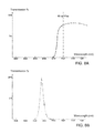
A blue color filter 708 is disposed in contact with a glass wafer 662 between glass wafer 662 and a lens 664. Blue color filter 708 may be a photo-resist coating. The transmission spectrum of blue color filter 708 is depicted in FIG. 8C. A UV-IR-cut filter 710 is disposed on a glass wafer 622 underneath a lens 620. UV-IR-cut filter 710 may be multilayer dielectric coatings. For example, the multilayer dielectric coatings may include 30 alternate layers of high and low refractive indexes. The daylight spectrum transmitted through UV-IR-cut filter 710 is depicted in FIG. 8D. The transmission spectra of UV-IR-cut filter 710 for 0°, 25°, 30°, and 35° incident light are depicted in FIG. 8E. For example, UV-IR-cut filter cuts the transmissions of wavelengths longer than 650 nm and shorter than 420 nm.
Blue filter 708 may be formed on either side of glass wafer 662, or either side of a second glass wafer 666. Similarly, UV-IR-cut filter 710 may be formed on either side of glass wafer 622, or either side of a second glass wafer 630, in accordance with the teachings of the present invention.
It is apparent that only R lens cube 502 requires an IR-cut filter. G lens cube 504 and B lens cube 506 require no IR-cut filter. C lens cube 508 uses a combined UV-IR-cut filter and no individual IR-cut filter is required. Thus, a cost saving in IR-cut filter coating can be achieved in accordance with the teachings of the present invention.
In another example, photo-resist coating red filter 704, green filter 706, and blue filter 708 are replaced with multilayer dielectric coated red filter 724, green filter 726, and blue filter 728, respectively, as depicted in FIGS. 7A and 7B, in accordance with the teachings of the present invention. The multilayer dielectric coated filters are bandpass filters. The transmission spectra of multilayer dielectric coated red filter 724, green filter 726, and blue filter 728 are shown in FIG. 9. For example, a multilayer dielectric coated color filter may include alternate layers of high and low refractive indexes. Since red filter 724 is a bandpass filter, an IR-cut filter, e.g., IR-cut filter 702, is no longer necessary. Thus, there would be an additional cost savings of an IR-cut filter coating. The bandpass filters will also alleviate the crosstalk of photo-resist filters as shown in FIG. 4.
In yet another example, the IR-cut filter, the UV-IR-cut filter, and the red, green, and blue filters may appropriately be coated as a filter 902 over a lens 960 on a glass wafer 962 and over the surface of glass wafer 962 surrounding lens 960, or a filter 904 over a lens 964 on the other side of glass wafer 962 and over the surface on glass wafer 962 surrounding lens 964 as depicted in FIG. 10, in accordance with the teachings of the present invention. FIG. 10 shows a lens cube 900, which may be one of lens cubes depicted in FIGS. 7A and 7B.
FIG. 11 is a block diagram illustrating an image sensor 800, in accordance with the teachings of the present invention. Image sensor 800 is one example implementation of image sensor 220 of FIG. 2, or image sensor 501 of FIG. 6. The illustrated example of image sensor 800 includes a pixel array 805, readout circuitry 810, function logic 815, and control circuitry 820. Pixel array 805 may be partitioned into four partitioned areas such as shown in FIG. 2 (not shown in FIG. 11).
Pixel array 805 is a two-dimensional (2D) array of an image sensor or pixels (e.g., pixels P1, P2, . . . , Pn). Each pixel may be a CMOS pixel or a CCD pixel. As illustrated, each pixel is arranged into a row (e.g., rows R1 to Ry) and a column (e.g., column C1 to Cx) to acquire image data of a person, place, object, etc., which can then be used to render a 2D image of the person, place, object, etc. In one example, pixel array 805 is a backside illuminated (BSI) image sensor. In one example, pixel array 805 is a frontside illuminated (FSI) image example, pixel array 805 is partitioned into a plurality of partitioned areas. Each partitioned area is covered by a color filter.
After each pixel has acquired its image data or image charge, the image data is readout by readout circuitry 810 and transferred to function logic 815. Readout circuitry 810 may include amplification circuitry, analog-to-digital (ADC) conversion circuitry, or otherwise. Function logic 815 may simply store the image data or even manipulate the image data by applying post image effects (e.g., crop, rotate, remove red eye, adjust brightness, adjust contrast, or otherwise). In one example, readout circuitry 810 may readout a row of image data at a time along readout column lines (illustrated) or may readout the image data using a variety of other techniques (not illustrated), such as a serial readout or a full parallel readout of all pixels simultaneously.
Control circuitry 820 is coupled to pixel array 805 to control operational characteristic of pixel array 805. For example, control circuitry 820 may generate a shutter signal for controlling image acquisition. In one embodiment, the shutter signal is a global shutter signal for simultaneously enabling all pixels within pixel array 805 to simultaneously capture their respective image data during a single acquisition window. In an alternative embodiment, the shutter signal is a rolling shutter signal whereby each row, column, or group of pixels is sequentially enabled during consecutive acquisition windows.
It is appreciated that the low profile image capture unit is not limited to 2×2 lens array, any size of lens array is possible. Accordingly, the image sensor is not limited to four partitioned areas, any number of partitioned areas is possible. The partitioned area of image sensor may be square or rectangular. The cross section of lens cube may be circular, ellipse, square, or rectangular. The image sensor may be a CMOS image sensor or a CCD.
The above description of illustrated examples of the present invention, including what is described in the Abstract, are not intended to be exhaustive or to be limitation to the precise forms disclosed. While specific embodiments of, and examples for, the invention are described herein for illustrative purposes, various equivalent modifications are possible without departing from the broader spirit and scope of the present invention. Indeed, it is appreciated that the specific example voltages, currents, frequencies, power range values, times, etc., are provided for explanation purposes and that other values may also be employed in other embodiments and examples in accordance with the teachings of the present invention.

Claims (17)

What is claimed is:
1. An apparatus, comprising:
an image sensor including N image sensor regions arranged thereon; and
N lens structures included in a lens array disposed proximate to the image sensor, each one of the N lens structures arranged to focus a single image onto a respective one of the N image sensor regions, the N lens structures including a first lens structure having a red color filter, a second lens structure having a green color filter, and a third lens structure having a blue color filter, each one of the N lens structures including a glass wafer and a lens formed on the glass wafer, wherein each one of the red color filter, the green color filter, and the blue color filter is one of coated on the glass wafer underneath the lens and coated over the lens on the glass wafer, wherein the first lens structure further includes an IR-cut filter including multilayer dielectric coatings, wherein the IR-cut filter is one of coated on the glass wafer underneath the lens and coated over the lens on the glass wafer.
2. The apparatus of claim 1 wherein the N lens structures further include a fourth lens structure having a UV-IR-cut filter including multilayer dielectric coatings, wherein the UV-IR-cut filter is one of coated on the glass wafer underneath the lens and coated over the lens on the glass wafer.
3. The apparatus of claim 1 wherein the red color filter, the green color filter, and the blue color filter comprise photo-resist coatings.
4. The apparatus of claim 1 wherein the red color filter, the green color filter, and the blue color filter comprise multilayer dielectric coatings.
5. The apparatus of claim 1 wherein the N lens structures include the first lens structure having a first focal length and positioned the first focal length away from the respective one of the N image sensor regions, the second lens structure having a second focal length and positioned the second focal length away from the respective one of the N image sensor regions, and the third lens structure having a third focal length and positioned the third focal length away from the respective one of the N image sensor regions, wherein the first focal length, the second focal length and the third focal length are different, wherein the first focal length corresponds with light having a red color, wherein the second focal length corresponds with light having a green color and wherein the third focal length corresponds with light having a blue color.
6. The apparatus of claim 5 wherein the N lens structures further include a fourth lens structure having a fourth focal length and positioned the fourth focal length away from the respective one of the N image sensor regions, wherein the fourth focal length is the same with one of the first focal length, the second length and the third focal length.
7. The apparatus of claim 1 wherein the N lens structures include the first lens structure having a first radius of curvature and positioned a focal length away from the respective one of the N image sensor regions, the second lens structure having a second radius of curvature and positioned the focal length away from the respective one of the N image sensor regions, and the third lens structure having a third radius of curvature and positioned the focal length away from the respective one of the N image sensor regions, wherein the first radius of curvature, the second radius of curvature and the third radius of curvature are different, wherein the first radius of curvature corresponds with light having a red color, wherein the second radius of curvature corresponds with light having a green color and wherein the third radius of curvature corresponds with light having a blue color.
8. The apparatus of claim 7 wherein the N lens structures further include a fourth lens structure having a fourth radius of curvature and positioned the focal length away from the respective one of the N image sensor regions, wherein the fourth radius of curvature is the same with one of the first radius of curvature, the second radius of curvature and the third radius of curvature.
9. An imaging system, comprising:
a pixel array including an image sensor having N image sensor regions arranged therein, wherein each one of the N image sensor regions has a plurality of pixels arranged therein;
N lens structures included in a lens array disposed proximate to the image sensor, each one of the N lens structures is arranged to focus a single image onto a respective one of the N image sensor regions, the N lens structures include a first lens structure having a red color filter, a second lens structure having a green color filter, and a third lens structure having a blue color filter, each one of the N lens structures including a glass wafer and a lens formed on the glass wafer, wherein each one of the red color filter, the green color filter, and the blue color filter is one of coated on the glass wafer underneath the lens and coated over the lens on the glass wafer, wherein the first lens structure further includes an IR-cut filter including multilayer dielectric coatings, wherein the IR-cut filter is one of coated on the glass wafer underneath the lens and coated over the lens on the glass wafer;
control circuitry coupled to the pixel array to control operation of the pixel array; and
readout circuitry coupled to the pixel array to readout image data from the plurality of pixels.
10. The imaging system of claim 9 further comprising function logic coupled to the readout circuitry to store the single image data readout from each one of the N image sensor regions.
11. The imaging system of claim 9 wherein the N lens structures further include a fourth lens structure having a UV-IR-cut filter including multilayer dielectric coatings, wherein the UV-IR-cut filter is one of coated on the glass wafer underneath the lens and coated over the lens on the glass wafer.
12. The imaging system of claim 9 wherein the red color filter, the green color filter, and the blue color filter comprise photo-resist coatings.
13. The imaging system of claim 9 wherein the red color filter, the green color filter, and the blue color filter comprise multilayer dielectric coatings.
14. The imaging system of claim 9 wherein the N lens structures include the first lens structure having a first focal length and positioned the first focal length away from the respective one of the N image sensor regions, the second lens structure having a second focal length and positioned the second focal length away from the respective one of the N image sensor regions, and the third lens structure having a third focal length and positioned the third focal length away from the respective one of the N image sensor regions, wherein the first focal length, the second focal length and the third focal length are different, wherein the first focal length corresponds with light having a red color, wherein the second focal length corresponds with light having a green color and wherein the third focal length corresponds with light having a blue color.
15. The imaging system of claim 14 wherein the N lens structures further include a fourth lens structure having a fourth focal length and positioned the fourth focal length away from the respective one of the N image sensor regions, wherein the fourth focal length is the same with one of the first focal length, the second length and the third focal length.
16. The imaging system of claim 9 wherein the N lens structures include the first lens structure having a first radius of curvature and positioned a focal length away from the respective one of the N image sensor regions, the second lens structure having a second radius of curvature and positioned the focal length away from the respective one of the N image sensor regions, and the third lens structure having a third radius of curvature and positioned the focal length away from the respective one of the N image sensor regions, wherein the first, second and third radii of curvature are different, wherein the first radius of curvature corresponds with light having a red color, wherein the second radius of curvature corresponds with light having a green color and wherein the third radius of curvature corresponds with light having a blue color.
17. The imaging system of claim 16 wherein the N lens structures further include a fourth lens structure having a fourth radius of curvature and positioned the focal length away from the respective one of the N image sensor regions, wherein the fourth radius of curvature is the same with one of the first radius of curvature, the second radius of curvature and the third radius of curvature.
US13/570,449 2012-08-09 2012-08-09 Lens array for partitioned image sensor having color filters Active 2033-07-03 US8988566B2 (en)

Priority Applications (4)

Application Number Priority Date Filing Date Title
US13/570,449 US8988566B2 (en) 2012-08-09 2012-08-09 Lens array for partitioned image sensor having color filters
TW102124070A TWI549273B (en) 2012-08-09 2013-07-04 Lens array for partitioned image sensor having color filters
CN201310313751.4A CN103579268B (en) 2012-08-09 2013-07-24 There is the lens arra of the segmentation imageing sensor of color filter
EP13179183.2A EP2696570B1 (en) 2012-08-09 2013-08-02 Lens array for partitioned image sensor having color filters

Applications Claiming Priority (1)

Application Number Priority Date Filing Date Title
US13/570,449 US8988566B2 (en) 2012-08-09 2012-08-09 Lens array for partitioned image sensor having color filters

Publications (2)

Publication Number Publication Date
US20140043507A1 US20140043507A1 (en) 2014-02-13
US8988566B2 true US8988566B2 (en) 2015-03-24

Family

ID=49083514

Family Applications (1)

Application Number Title Priority Date Filing Date
US13/570,449 Active 2033-07-03 US8988566B2 (en) 2012-08-09 2012-08-09 Lens array for partitioned image sensor having color filters

Country Status (4)

Country Link
US (1) US8988566B2 (en)
EP (1) EP2696570B1 (en)
CN (1) CN103579268B (en)
TW (1) TWI549273B (en)

Cited By (2)

* Cited by examiner, † Cited by third party
Publication number Priority date Publication date Assignee Title
US20150281601A1 (en) * 2014-03-25 2015-10-01 INVIS Technologies Corporation Modular Packaging and Optical System for Multi-Aperture and Multi-Spectral Camera Core
US11366011B2 (en) 2019-02-13 2022-06-21 Viavi Solutions Inc. Optical device

Families Citing this family (56)

* Cited by examiner, † Cited by third party
Publication number Priority date Publication date Assignee Title
US8902321B2 (en) 2008-05-20 2014-12-02 Pelican Imaging Corporation Capturing and processing of images using monolithic camera array with heterogeneous imagers
US11792538B2 (en) 2008-05-20 2023-10-17 Adeia Imaging Llc Capturing and processing of images including occlusions focused on an image sensor by a lens stack array
US8866920B2 (en) 2008-05-20 2014-10-21 Pelican Imaging Corporation Capturing and processing of images using monolithic camera array with heterogeneous imagers
WO2011063347A2 (en) 2009-11-20 2011-05-26 Pelican Imaging Corporation Capturing and processing of images using monolithic camera array with heterogeneous imagers
SG10201503516VA (en) 2010-05-12 2015-06-29 Pelican Imaging Corp Architectures for imager arrays and array cameras
US8878950B2 (en) 2010-12-14 2014-11-04 Pelican Imaging Corporation Systems and methods for synthesizing high resolution images using super-resolution processes
EP2708019B1 (en) 2011-05-11 2019-10-16 FotoNation Limited Systems and methods for transmitting and receiving array camera image data
US20130265459A1 (en) 2011-06-28 2013-10-10 Pelican Imaging Corporation Optical arrangements for use with an array camera
WO2013043761A1 (en) 2011-09-19 2013-03-28 Pelican Imaging Corporation Determining depth from multiple views of a scene that include aliasing using hypothesized fusion
EP2761534B1 (en) 2011-09-28 2020-11-18 FotoNation Limited Systems for encoding light field image files
WO2013126578A1 (en) 2012-02-21 2013-08-29 Pelican Imaging Corporation Systems and methods for the manipulation of captured light field image data
US9210392B2 (en) 2012-05-01 2015-12-08 Pelican Imaging Coporation Camera modules patterned with pi filter groups
US8791403B2 (en) * 2012-06-01 2014-07-29 Omnivision Technologies, Inc. Lens array for partitioned image sensor to focus a single image onto N image sensor regions
WO2014005123A1 (en) 2012-06-28 2014-01-03 Pelican Imaging Corporation Systems and methods for detecting defective camera arrays, optic arrays, and sensors
US20140002674A1 (en) 2012-06-30 2014-01-02 Pelican Imaging Corporation Systems and Methods for Manufacturing Camera Modules Using Active Alignment of Lens Stack Arrays and Sensors
AU2013305770A1 (en) 2012-08-21 2015-02-26 Pelican Imaging Corporation Systems and methods for parallax detection and correction in images captured using array cameras
US20140055632A1 (en) 2012-08-23 2014-02-27 Pelican Imaging Corporation Feature based high resolution motion estimation from low resolution images captured using an array source
EP4307659A1 (en) 2012-09-28 2024-01-17 Adeia Imaging LLC Generating images from light fields utilizing virtual viewpoints
WO2014078443A1 (en) 2012-11-13 2014-05-22 Pelican Imaging Corporation Systems and methods for array camera focal plane control
WO2014130849A1 (en) 2013-02-21 2014-08-28 Pelican Imaging Corporation Generating compressed light field representation data
US9374512B2 (en) 2013-02-24 2016-06-21 Pelican Imaging Corporation Thin form factor computational array cameras and modular array cameras
WO2014138695A1 (en) 2013-03-08 2014-09-12 Pelican Imaging Corporation Systems and methods for measuring scene information while capturing images using array cameras
US8866912B2 (en) 2013-03-10 2014-10-21 Pelican Imaging Corporation System and methods for calibration of an array camera using a single captured image
WO2014164909A1 (en) 2013-03-13 2014-10-09 Pelican Imaging Corporation Array camera architecture implementing quantum film sensors
US9106784B2 (en) 2013-03-13 2015-08-11 Pelican Imaging Corporation Systems and methods for controlling aliasing in images captured by an array camera for use in super-resolution processing
US9124831B2 (en) 2013-03-13 2015-09-01 Pelican Imaging Corporation System and methods for calibration of an array camera
WO2014165244A1 (en) 2013-03-13 2014-10-09 Pelican Imaging Corporation Systems and methods for synthesizing images from image data captured by an array camera using restricted depth of field depth maps in which depth estimation precision varies
WO2014159779A1 (en) 2013-03-14 2014-10-02 Pelican Imaging Corporation Systems and methods for reducing motion blur in images or video in ultra low light with array cameras
WO2014153098A1 (en) 2013-03-14 2014-09-25 Pelican Imaging Corporation Photmetric normalization in array cameras
US9438888B2 (en) 2013-03-15 2016-09-06 Pelican Imaging Corporation Systems and methods for stereo imaging with camera arrays
US9497429B2 (en) 2013-03-15 2016-11-15 Pelican Imaging Corporation Extended color processing on pelican array cameras
US9445003B1 (en) 2013-03-15 2016-09-13 Pelican Imaging Corporation Systems and methods for synthesizing high resolution images using image deconvolution based on motion and depth information
US10122993B2 (en) 2013-03-15 2018-11-06 Fotonation Limited Autofocus system for a conventional camera that uses depth information from an array camera
WO2015041496A1 (en) * 2013-09-23 2015-03-26 엘지이노텍 주식회사 Camera module and manufacturing method for same
WO2015048694A2 (en) 2013-09-27 2015-04-02 Pelican Imaging Corporation Systems and methods for depth-assisted perspective distortion correction
CN103557459B (en) * 2013-11-06 2016-03-02 郑州中原显示技术有限公司 The three-primary color LED lamp that light-emitting area is not identical
WO2015070105A1 (en) 2013-11-07 2015-05-14 Pelican Imaging Corporation Methods of manufacturing array camera modules incorporating independently aligned lens stacks
US10119808B2 (en) 2013-11-18 2018-11-06 Fotonation Limited Systems and methods for estimating depth from projected texture using camera arrays
WO2015081279A1 (en) 2013-11-26 2015-06-04 Pelican Imaging Corporation Array camera configurations incorporating multiple constituent array cameras
WO2015134996A1 (en) 2014-03-07 2015-09-11 Pelican Imaging Corporation System and methods for depth regularization and semiautomatic interactive matting using rgb-d images
US9270953B2 (en) * 2014-05-16 2016-02-23 Omnivision Technologies, Inc. Wafer level camera having movable color filter grouping
US9521319B2 (en) * 2014-06-18 2016-12-13 Pelican Imaging Corporation Array cameras and array camera modules including spectral filters disposed outside of a constituent image sensor
KR20170063827A (en) 2014-09-29 2017-06-08 포토네이션 케이맨 리미티드 Systems and methods for dynamic calibration of array cameras
US9942474B2 (en) 2015-04-17 2018-04-10 Fotonation Cayman Limited Systems and methods for performing high speed video capture and depth estimation using array cameras
CN105223756B (en) * 2015-10-06 2018-03-09 瑞声光电科技(常州)有限公司 Array camera lens module
US10313642B2 (en) * 2017-01-18 2019-06-04 Omnivision Technologies, Inc. Imaging system having dual image sensors
US10482618B2 (en) 2017-08-21 2019-11-19 Fotonation Limited Systems and methods for hybrid depth regularization
WO2021055585A1 (en) 2019-09-17 2021-03-25 Boston Polarimetrics, Inc. Systems and methods for surface modeling using polarization cues
BR112022006617A2 (en) 2019-10-07 2022-06-28 Boston Polarimetrics Inc SYSTEMS AND METHODS FOR SENSOR DETECTION OF NORMALS ON THE SURFACE WITH POLARIZATION
EP4066001A4 (en) 2019-11-30 2024-01-24 Boston Polarimetrics Inc Systems and methods for transparent object segmentation using polarization cues
KR20220132620A (en) 2020-01-29 2022-09-30 인트린식 이노베이션 엘엘씨 Systems and methods for characterizing object pose detection and measurement systems
JP2023511747A (en) 2020-01-30 2023-03-22 イントリンジック イノベーション エルエルシー Systems and methods for synthesizing data for training statistical models with different imaging modalities, including polarization imaging
WO2021243088A1 (en) 2020-05-27 2021-12-02 Boston Polarimetrics, Inc. Multi-aperture polarization optical systems using beam splitters
US11290658B1 (en) 2021-04-15 2022-03-29 Boston Polarimetrics, Inc. Systems and methods for camera exposure control
US11954886B2 (en) 2021-04-15 2024-04-09 Intrinsic Innovation Llc Systems and methods for six-degree of freedom pose estimation of deformable objects
US11689813B2 (en) 2021-07-01 2023-06-27 Intrinsic Innovation Llc Systems and methods for high dynamic range imaging using crossed polarizers

Citations (18)

* Cited by examiner, † Cited by third party
Publication number Priority date Publication date Assignee Title
EP1067802A2 (en) 1999-06-30 2001-01-10 Canon Kabushiki Kaisha Colour image pickup apparatus
US20020089596A1 (en) 2000-12-28 2002-07-11 Yasuo Suda Image sensing apparatus
US20060023314A1 (en) 2004-07-27 2006-02-02 Boettiger Ulrich C Controlling lens shape in a microlens array
US20060226452A1 (en) 2005-04-08 2006-10-12 Konica Minolta Opto, Inc. Solid-state image pickup device and the manufacture method thereof
US20070008421A1 (en) 2005-07-07 2007-01-11 Hsin-Ping Wu Method for forming microlenses of different curvatures and fabricating process of solid-state image sensor
US20070126898A1 (en) * 2004-09-27 2007-06-07 Digital Optics Corporation Thin camera and associated methods
US7247851B2 (en) 2003-11-10 2007-07-24 Matsushita Electric Industrial Co., Ltd. Imaging device and an imaging method
US20080049126A1 (en) 2006-08-28 2008-02-28 Micron Technology, Inc. Color filter array and method of fabrication and use
US20080128843A1 (en) 2006-11-30 2008-06-05 Lee Sang Uk Image Sensor and Fabricating Method Thereof
US20080142685A1 (en) 2006-12-13 2008-06-19 Gazeley William G Integrated image sensor having a color-filtering microlens, and related system and method
US7453510B2 (en) * 2003-12-11 2008-11-18 Nokia Corporation Imaging device
US20100065897A1 (en) 2008-09-16 2010-03-18 Sung Ho Jun CMOS Image Sensor and Method for Fabricating the Same
EP2214405A2 (en) 2009-02-02 2010-08-04 L-3 Communications Cincinnati Electronics Multi-channel imaging devices
US7812869B2 (en) 2007-05-11 2010-10-12 Aptina Imaging Corporation Configurable pixel array system and method
US20110122308A1 (en) * 2009-11-20 2011-05-26 Pelican Imaging Corporation Capturing and processing of images using monolithic camera array with heterogeneous imagers
US20110194019A1 (en) 2010-02-11 2011-08-11 San-Woei Shyu Optical imaging lens and array thereof
US20120104525A1 (en) 2008-02-11 2012-05-03 Omnivision Technologies, Inc. Image sensor with color pixels having uniform light absorption depths
US20130320195A1 (en) 2012-06-01 2013-12-05 Omnivision Technologies, Inc. Lens array for partitioned image sensor

Family Cites Families (1)

* Cited by examiner, † Cited by third party
Publication number Priority date Publication date Assignee Title
CN100474003C (en) * 2006-04-04 2009-04-01 精工爱普生株式会社 Optical multilayer filter, and electronic apparatus

Patent Citations (18)

* Cited by examiner, † Cited by third party
Publication number Priority date Publication date Assignee Title
EP1067802A2 (en) 1999-06-30 2001-01-10 Canon Kabushiki Kaisha Colour image pickup apparatus
US20020089596A1 (en) 2000-12-28 2002-07-11 Yasuo Suda Image sensing apparatus
US7247851B2 (en) 2003-11-10 2007-07-24 Matsushita Electric Industrial Co., Ltd. Imaging device and an imaging method
US7453510B2 (en) * 2003-12-11 2008-11-18 Nokia Corporation Imaging device
US20060023314A1 (en) 2004-07-27 2006-02-02 Boettiger Ulrich C Controlling lens shape in a microlens array
US20070126898A1 (en) * 2004-09-27 2007-06-07 Digital Optics Corporation Thin camera and associated methods
US20060226452A1 (en) 2005-04-08 2006-10-12 Konica Minolta Opto, Inc. Solid-state image pickup device and the manufacture method thereof
US20070008421A1 (en) 2005-07-07 2007-01-11 Hsin-Ping Wu Method for forming microlenses of different curvatures and fabricating process of solid-state image sensor
US20080049126A1 (en) 2006-08-28 2008-02-28 Micron Technology, Inc. Color filter array and method of fabrication and use
US20080128843A1 (en) 2006-11-30 2008-06-05 Lee Sang Uk Image Sensor and Fabricating Method Thereof
US20080142685A1 (en) 2006-12-13 2008-06-19 Gazeley William G Integrated image sensor having a color-filtering microlens, and related system and method
US7812869B2 (en) 2007-05-11 2010-10-12 Aptina Imaging Corporation Configurable pixel array system and method
US20120104525A1 (en) 2008-02-11 2012-05-03 Omnivision Technologies, Inc. Image sensor with color pixels having uniform light absorption depths
US20100065897A1 (en) 2008-09-16 2010-03-18 Sung Ho Jun CMOS Image Sensor and Method for Fabricating the Same
EP2214405A2 (en) 2009-02-02 2010-08-04 L-3 Communications Cincinnati Electronics Multi-channel imaging devices
US20110122308A1 (en) * 2009-11-20 2011-05-26 Pelican Imaging Corporation Capturing and processing of images using monolithic camera array with heterogeneous imagers
US20110194019A1 (en) 2010-02-11 2011-08-11 San-Woei Shyu Optical imaging lens and array thereof
US20130320195A1 (en) 2012-06-01 2013-12-05 Omnivision Technologies, Inc. Lens array for partitioned image sensor

Non-Patent Citations (6)

* Cited by examiner, † Cited by third party
Title
EP 13167195.0-European Search Report and Search Opinion, dated Nov. 6, 2013 (11 pages).
EP 13167195.0—European Search Report and Search Opinion, dated Nov. 6, 2013 (11 pages).
EP 13179183.2-Extended European Search Report, dated Jul. 16, 2014 (7 pages).
EP 13179183.2—Extended European Search Report, dated Jul. 16, 2014 (7 pages).
TW Patent Application No. 102115760-First Taiwanese Office Action, issued Sep. 24, 2014, with Search Report and English Translation (14 pages).
TW Patent Application No. 102115760—First Taiwanese Office Action, issued Sep. 24, 2014, with Search Report and English Translation (14 pages).

Cited By (3)

* Cited by examiner, † Cited by third party
Publication number Priority date Publication date Assignee Title
US20150281601A1 (en) * 2014-03-25 2015-10-01 INVIS Technologies Corporation Modular Packaging and Optical System for Multi-Aperture and Multi-Spectral Camera Core
US11366011B2 (en) 2019-02-13 2022-06-21 Viavi Solutions Inc. Optical device
US11913833B2 (en) 2019-02-13 2024-02-27 Viavi Solutions Inc. Optical device

Also Published As

Publication number Publication date
EP2696570A3 (en) 2014-08-13
CN103579268B (en) 2016-09-07
EP2696570B1 (en) 2019-07-17
TW201407757A (en) 2014-02-16
US20140043507A1 (en) 2014-02-13
TWI549273B (en) 2016-09-11
EP2696570A2 (en) 2014-02-12
CN103579268A (en) 2014-02-12

Similar Documents

Publication Publication Date Title
US8988566B2 (en) Lens array for partitioned image sensor having color filters
JP7171652B2 (en) Solid-state image sensor and electronic equipment
US10297629B2 (en) Image sensors with in-pixel lens arrays
US9270953B2 (en) Wafer level camera having movable color filter grouping
US8791403B2 (en) Lens array for partitioned image sensor to focus a single image onto N image sensor regions
US8530814B2 (en) Solid-state imaging device with a planarized lens layer method of manufacturing the same, and electronic apparatus
US20130015545A1 (en) Solid-state imaging device, manufacturing method of solid-state imaging device and electronic apparatus
US10187595B2 (en) Solid-state image sensor
US10506187B2 (en) Image sensor having dual microlenses for each auto-focus (AF) pixel
US9386203B2 (en) Compact spacer in multi-lens array module
US8389921B2 (en) Image sensor having array of pixels and metal reflectors with widths scaled based on distance from center of the array
US20200348455A1 (en) Imaging systems with improved microlenses
US9595551B2 (en) Solid-state imaging device and electronic apparatus
WO2016194620A1 (en) Solid-state imaging device and electronic device
JP2006196503A (en) Solid-state imaging device and its manufacturing method
TW202412292A (en) Half quad photodiode (qpd) to improve qpd channel imbalance

Legal Events

Date Code Title Description
AS Assignment

Owner name: OMNIVISION TECHNOLOGIES, INC., CALIFORNIA

Free format text: ASSIGNMENT OF ASSIGNORS INTEREST;ASSIGNORS:WANG, CHIA-CHING;DENG, JAU-JAN;HSU, YUN-CHIANG;REEL/FRAME:028756/0772

Effective date: 20120807

STCF Information on status: patent grant

Free format text: PATENTED CASE

MAFP Maintenance fee payment

Free format text: PAYMENT OF MAINTENANCE FEE, 4TH YEAR, LARGE ENTITY (ORIGINAL EVENT CODE: M1551); ENTITY STATUS OF PATENT OWNER: LARGE ENTITY

Year of fee payment: 4

MAFP Maintenance fee payment

Free format text: PAYMENT OF MAINTENANCE FEE, 8TH YEAR, LARGE ENTITY (ORIGINAL EVENT CODE: M1552); ENTITY STATUS OF PATENT OWNER: LARGE ENTITY

Year of fee payment: 8