US8964286B2 - System and device for non-destructive Raman analysis - Google Patents
System and device for non-destructive Raman analysis Download PDFInfo
- Publication number
- US8964286B2 US8964286B2 US14/221,418 US201414221418A US8964286B2 US 8964286 B2 US8964286 B2 US 8964286B2 US 201414221418 A US201414221418 A US 201414221418A US 8964286 B2 US8964286 B2 US 8964286B2
- Authority
- US
- United States
- Prior art keywords
- extender
- raman
- optical
- microspectrometer
- raman microspectrometer
- Prior art date
- Legal status (The legal status is an assumption and is not a legal conclusion. Google has not performed a legal analysis and makes no representation as to the accuracy of the status listed.)
- Active
Links
- 238000001069 Raman spectroscopy Methods 0.000 title claims abstract description 102
- 238000004458 analytical method Methods 0.000 title claims abstract description 40
- 230000001066 destructive effect Effects 0.000 title claims abstract description 10
- 230000003287 optical effect Effects 0.000 claims abstract description 87
- 239000004606 Fillers/Extenders Substances 0.000 claims abstract description 60
- 238000009607 mammography Methods 0.000 claims abstract description 28
- 230000000153 supplemental effect Effects 0.000 claims abstract description 27
- BUGBHKTXTAQXES-UHFFFAOYSA-N Selenium Chemical compound [Se] BUGBHKTXTAQXES-UHFFFAOYSA-N 0.000 claims description 33
- 229910052711 selenium Inorganic materials 0.000 claims description 33
- 239000011669 selenium Substances 0.000 claims description 33
- 230000035945 sensitivity Effects 0.000 claims description 12
- 239000000725 suspension Substances 0.000 claims description 10
- 239000000463 material Substances 0.000 claims description 9
- 238000003384 imaging method Methods 0.000 claims description 6
- 238000012546 transfer Methods 0.000 claims description 5
- 230000003247 decreasing effect Effects 0.000 claims description 2
- 239000007788 liquid Substances 0.000 claims description 2
- 239000007787 solid Substances 0.000 claims 1
- 230000008439 repair process Effects 0.000 abstract description 17
- 238000004519 manufacturing process Methods 0.000 abstract description 15
- 230000006378 damage Effects 0.000 abstract description 7
- 238000012360 testing method Methods 0.000 abstract description 6
- 230000007423 decrease Effects 0.000 abstract description 2
- 238000000034 method Methods 0.000 description 19
- 230000007547 defect Effects 0.000 description 14
- 230000008569 process Effects 0.000 description 13
- 238000010586 diagram Methods 0.000 description 9
- 238000010183 spectrum analysis Methods 0.000 description 5
- 239000011521 glass Substances 0.000 description 4
- 238000012986 modification Methods 0.000 description 4
- 230000004048 modification Effects 0.000 description 4
- 230000004044 response Effects 0.000 description 4
- 230000008901 benefit Effects 0.000 description 3
- 238000004891 communication Methods 0.000 description 3
- 238000004590 computer program Methods 0.000 description 3
- 239000013078 crystal Substances 0.000 description 3
- 238000001228 spectrum Methods 0.000 description 3
- XKRFYHLGVUSROY-UHFFFAOYSA-N Argon Chemical compound [Ar] XKRFYHLGVUSROY-UHFFFAOYSA-N 0.000 description 2
- IJGRMHOSHXDMSA-UHFFFAOYSA-N Atomic nitrogen Chemical compound N#N IJGRMHOSHXDMSA-UHFFFAOYSA-N 0.000 description 2
- 230000005540 biological transmission Effects 0.000 description 2
- 230000008859 change Effects 0.000 description 2
- 238000012512 characterization method Methods 0.000 description 2
- 230000008878 coupling Effects 0.000 description 2
- 238000010168 coupling process Methods 0.000 description 2
- 238000005859 coupling reaction Methods 0.000 description 2
- 238000002425 crystallisation Methods 0.000 description 2
- 230000008025 crystallization Effects 0.000 description 2
- 238000013461 design Methods 0.000 description 2
- 238000005516 engineering process Methods 0.000 description 2
- 239000012530 fluid Substances 0.000 description 2
- 238000007479 molecular analysis Methods 0.000 description 2
- 239000004065 semiconductor Substances 0.000 description 2
- 239000010409 thin film Substances 0.000 description 2
- 238000012795 verification Methods 0.000 description 2
- 238000001530 Raman microscopy Methods 0.000 description 1
- 239000000654 additive Substances 0.000 description 1
- XAGFODPZIPBFFR-UHFFFAOYSA-N aluminium Chemical compound [Al] XAGFODPZIPBFFR-UHFFFAOYSA-N 0.000 description 1
- 229910052782 aluminium Inorganic materials 0.000 description 1
- 238000005280 amorphization Methods 0.000 description 1
- 230000003466 anti-cipated effect Effects 0.000 description 1
- 229910052786 argon Inorganic materials 0.000 description 1
- 230000004888 barrier function Effects 0.000 description 1
- 239000003990 capacitor Substances 0.000 description 1
- JJWKPURADFRFRB-UHFFFAOYSA-N carbonyl sulfide Chemical compound O=C=S JJWKPURADFRFRB-UHFFFAOYSA-N 0.000 description 1
- 239000011248 coating agent Substances 0.000 description 1
- 238000000576 coating method Methods 0.000 description 1
- 238000004624 confocal microscopy Methods 0.000 description 1
- 230000002950 deficient Effects 0.000 description 1
- 230000001419 dependent effect Effects 0.000 description 1
- 230000005684 electric field Effects 0.000 description 1
- 230000005284 excitation Effects 0.000 description 1
- 230000005281 excited state Effects 0.000 description 1
- 239000000835 fiber Substances 0.000 description 1
- 239000007789 gas Substances 0.000 description 1
- 239000003365 glass fiber Substances 0.000 description 1
- 239000001307 helium Substances 0.000 description 1
- 229910052734 helium Inorganic materials 0.000 description 1
- SWQJXJOGLNCZEY-UHFFFAOYSA-N helium atom Chemical compound [He] SWQJXJOGLNCZEY-UHFFFAOYSA-N 0.000 description 1
- 238000007689 inspection Methods 0.000 description 1
- 238000011835 investigation Methods 0.000 description 1
- 239000011159 matrix material Substances 0.000 description 1
- 230000007246 mechanism Effects 0.000 description 1
- 238000001634 microspectroscopy Methods 0.000 description 1
- 229910052757 nitrogen Inorganic materials 0.000 description 1
- 239000004033 plastic Substances 0.000 description 1
- 230000010287 polarization Effects 0.000 description 1
- 229920000052 poly(p-xylylene) Polymers 0.000 description 1
- 238000012545 processing Methods 0.000 description 1
- 230000005855 radiation Effects 0.000 description 1
- 230000003595 spectral effect Effects 0.000 description 1
- 229910001220 stainless steel Inorganic materials 0.000 description 1
- 239000010935 stainless steel Substances 0.000 description 1
- 238000012956 testing procedure Methods 0.000 description 1
- 238000012549 training Methods 0.000 description 1
Images


Classifications
-
- G—PHYSICS
- G01—MEASURING; TESTING
- G01J—MEASUREMENT OF INTENSITY, VELOCITY, SPECTRAL CONTENT, POLARISATION, PHASE OR PULSE CHARACTERISTICS OF INFRARED, VISIBLE OR ULTRAVIOLET LIGHT; COLORIMETRY; RADIATION PYROMETRY
- G01J3/00—Spectrometry; Spectrophotometry; Monochromators; Measuring colours
- G01J3/02—Details
- G01J3/0205—Optical elements not provided otherwise, e.g. optical manifolds, diffusers, windows
- G01J3/0218—Optical elements not provided otherwise, e.g. optical manifolds, diffusers, windows using optical fibers
-
- G—PHYSICS
- G01—MEASURING; TESTING
- G01J—MEASUREMENT OF INTENSITY, VELOCITY, SPECTRAL CONTENT, POLARISATION, PHASE OR PULSE CHARACTERISTICS OF INFRARED, VISIBLE OR ULTRAVIOLET LIGHT; COLORIMETRY; RADIATION PYROMETRY
- G01J3/00—Spectrometry; Spectrophotometry; Monochromators; Measuring colours
- G01J3/28—Investigating the spectrum
- G01J3/44—Raman spectrometry; Scattering spectrometry ; Fluorescence spectrometry
-
- G—PHYSICS
- G01—MEASURING; TESTING
- G01J—MEASUREMENT OF INTENSITY, VELOCITY, SPECTRAL CONTENT, POLARISATION, PHASE OR PULSE CHARACTERISTICS OF INFRARED, VISIBLE OR ULTRAVIOLET LIGHT; COLORIMETRY; RADIATION PYROMETRY
- G01J3/00—Spectrometry; Spectrophotometry; Monochromators; Measuring colours
- G01J3/02—Details
- G01J3/0202—Mechanical elements; Supports for optical elements
-
- G—PHYSICS
- G01—MEASURING; TESTING
- G01J—MEASUREMENT OF INTENSITY, VELOCITY, SPECTRAL CONTENT, POLARISATION, PHASE OR PULSE CHARACTERISTICS OF INFRARED, VISIBLE OR ULTRAVIOLET LIGHT; COLORIMETRY; RADIATION PYROMETRY
- G01J3/00—Spectrometry; Spectrophotometry; Monochromators; Measuring colours
- G01J3/02—Details
- G01J3/0205—Optical elements not provided otherwise, e.g. optical manifolds, diffusers, windows
- G01J3/0208—Optical elements not provided otherwise, e.g. optical manifolds, diffusers, windows using focussing or collimating elements, e.g. lenses or mirrors; performing aberration correction
-
- G—PHYSICS
- G01—MEASURING; TESTING
- G01J—MEASUREMENT OF INTENSITY, VELOCITY, SPECTRAL CONTENT, POLARISATION, PHASE OR PULSE CHARACTERISTICS OF INFRARED, VISIBLE OR ULTRAVIOLET LIGHT; COLORIMETRY; RADIATION PYROMETRY
- G01J3/00—Spectrometry; Spectrophotometry; Monochromators; Measuring colours
- G01J3/02—Details
- G01J3/0205—Optical elements not provided otherwise, e.g. optical manifolds, diffusers, windows
- G01J3/021—Optical elements not provided otherwise, e.g. optical manifolds, diffusers, windows using plane or convex mirrors, parallel phase plates, or particular reflectors
-
- G—PHYSICS
- G01—MEASURING; TESTING
- G01J—MEASUREMENT OF INTENSITY, VELOCITY, SPECTRAL CONTENT, POLARISATION, PHASE OR PULSE CHARACTERISTICS OF INFRARED, VISIBLE OR ULTRAVIOLET LIGHT; COLORIMETRY; RADIATION PYROMETRY
- G01J3/00—Spectrometry; Spectrophotometry; Monochromators; Measuring colours
- G01J3/02—Details
- G01J3/0256—Compact construction
-
- G—PHYSICS
- G01—MEASURING; TESTING
- G01J—MEASUREMENT OF INTENSITY, VELOCITY, SPECTRAL CONTENT, POLARISATION, PHASE OR PULSE CHARACTERISTICS OF INFRARED, VISIBLE OR ULTRAVIOLET LIGHT; COLORIMETRY; RADIATION PYROMETRY
- G01J3/00—Spectrometry; Spectrophotometry; Monochromators; Measuring colours
- G01J3/02—Details
- G01J3/027—Control of working procedures of a spectrometer; Failure detection; Bandwidth calculation
-
- G—PHYSICS
- G01—MEASURING; TESTING
- G01J—MEASUREMENT OF INTENSITY, VELOCITY, SPECTRAL CONTENT, POLARISATION, PHASE OR PULSE CHARACTERISTICS OF INFRARED, VISIBLE OR ULTRAVIOLET LIGHT; COLORIMETRY; RADIATION PYROMETRY
- G01J3/00—Spectrometry; Spectrophotometry; Monochromators; Measuring colours
- G01J3/02—Details
- G01J3/0291—Housings; Spectrometer accessories; Spatial arrangement of elements, e.g. folded path arrangements
-
- G—PHYSICS
- G01—MEASURING; TESTING
- G01J—MEASUREMENT OF INTENSITY, VELOCITY, SPECTRAL CONTENT, POLARISATION, PHASE OR PULSE CHARACTERISTICS OF INFRARED, VISIBLE OR ULTRAVIOLET LIGHT; COLORIMETRY; RADIATION PYROMETRY
- G01J3/00—Spectrometry; Spectrophotometry; Monochromators; Measuring colours
- G01J3/28—Investigating the spectrum
- G01J3/44—Raman spectrometry; Scattering spectrometry ; Fluorescence spectrometry
- G01J3/4412—Scattering spectrometry
-
- G—PHYSICS
- G01—MEASURING; TESTING
- G01N—INVESTIGATING OR ANALYSING MATERIALS BY DETERMINING THEIR CHEMICAL OR PHYSICAL PROPERTIES
- G01N21/00—Investigating or analysing materials by the use of optical means, i.e. using sub-millimetre waves, infrared, visible or ultraviolet light
- G01N21/84—Systems specially adapted for particular applications
- G01N21/88—Investigating the presence of flaws or contamination
- G01N21/95—Investigating the presence of flaws or contamination characterised by the material or shape of the object to be examined
-
- G—PHYSICS
- G01—MEASURING; TESTING
- G01N—INVESTIGATING OR ANALYSING MATERIALS BY DETERMINING THEIR CHEMICAL OR PHYSICAL PROPERTIES
- G01N21/00—Investigating or analysing materials by the use of optical means, i.e. using sub-millimetre waves, infrared, visible or ultraviolet light
- G01N21/62—Systems in which the material investigated is excited whereby it emits light or causes a change in wavelength of the incident light
- G01N21/63—Systems in which the material investigated is excited whereby it emits light or causes a change in wavelength of the incident light optically excited
- G01N21/65—Raman scattering
-
- G—PHYSICS
- G02—OPTICS
- G02B—OPTICAL ELEMENTS, SYSTEMS OR APPARATUS
- G02B21/00—Microscopes
- G02B21/24—Base structure
Definitions
- a microspectrometer system for non-destructive analysis of an oversized sample includes a microspectrometer comprising an optical microscope coupled to a spectrometer by an optical transfer tube, where the optical microscope includes a lens and an existing stage.
- An extender is removably coupled to the optical microscope.
- the extender has a proximal orifice disposed adjacent to the lens and a distal orifice, where the extender extends an optical reach of the microscope to the distal orifice.
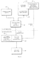
- FIG. 1 is a diagram illustrating a prior art Raman microspectrometer
- an improved Raman microspectrometer system extends the optical reach and analysis range of an existing Raman microspectrometer to allow analysis and/or repair of an oversized sample.
- an oversized sample shall mean any sample that exceeds the travel capabilities of an existing stage of the existing Raman microspectrometer in any one of an x, y or z dimensions.
- the improved Raman microspectrometer system includes an extender for extending the optical reach of the existing microspectrometer and a supplemental stage which extends the analysis range of the existing microspectrometer by providing travel capabilities for non-destructive analysis of an entire oversized sample.
- Such an arrangement decreases manufacturing costs associated with testing oversized samples such as mammography panels, enabling analysis and/or repair to be performed without destruction.
- such an arrangement increases the speed and accuracy of defect analysis and repair because it allows coordinate information received from a panel testing procedure to be used by software to quickly and accurately pinpoint problem areas in the panel.
Abstract
Description
| TABLE 1 |
| Conditions for Testing Sensitivity of a Raman Microspectrometer for |
| Presence of Crystallized Selenium in an Otherwise Amorpohous Selenium |
| Mammography Panel |
| With An Optical Extension | ||
| (Length = 539 mm; | ||
| Mirror-to-Mirror Length = 454 mm; | ||
| Raman Microspectrometer | Width = 62 mm; | |
| Parameter | Height = 50 mm) | Without An Optical Extension |
| Spectrometer | Almega XR | Almega XR |
| Laser | 780 nm | 780 nm |
| Laser Power Level | 3.5 mW (10% of 35 mW) | 3.5 mW (10% of 35 mW) |
| Laser Polarization | parallel | parallel |
| Cosmic Ray Threshold | low | low |
| Grating | 360 lines/mm | 360 lines/mm |
| Spectrograph Aperture for | (1) 25 μm pinhole and (2) 100 μm | (1) 25 μm pinhole and (2) 100 μm |
| Confocality | pinhole | pinhole |
| Sample Position | microscope | microscope |
| CCD Camera Temperature | −49° C. | −49° C. |
| CCD Rows Binned | 1.256 | 1.256 |
| CCD Binning | on chip | on chip |
| Spectral Resolution | 1.9285 cm−1 | 1.9285 cm−2 |
| Total Number of Data Points | 3514 | 3514 |
| X-Axis | Raman shift (cm−1) | Raman shift (cm−1) |
| Y-Axis | Raman Intensity | Raman Intensity |
| First X Value | 93.4795 cm−1 | 93.4795 cm−2 |
| Last X Value | 3480.8311 cm−1 | 3480.8311 cm−2 |
| Data Spacing | 0.964233 cm−1 | 0.964233 cm−2 |
| Sample Format | Mammography Panel (11.288″ × | Mammography Panel (11.288″ × |
| 9.877″) | 9.877″) | |
| with amorphous selenium | with amorphous selenium | |
| Sample Position on | gate side roll-off edge | gate side roll-off edge |
| Mammography Panel | ||
| Raman Microscope Objective | Olympus BX51TRF/UMPlanF1/ | Olympus BX51TRF/UMPlanF1/ |
| 20x/0.46 BD | 20x/0.46 BD | |
| Focal Plane | lower selenium surface through | lower selenium surface through |
| support glass and TFT glass of | support glass and TFT glass of | |
| mammography panel | mammography panel | |
Claims (20)
Priority Applications (1)
| Application Number | Priority Date | Filing Date | Title |
|---|---|---|---|
| US14/221,418 US8964286B2 (en) | 2008-07-24 | 2014-03-21 | System and device for non-destructive Raman analysis |
Applications Claiming Priority (3)
| Application Number | Priority Date | Filing Date | Title |
|---|---|---|---|
| US12/179,251 US20100020393A1 (en) | 2008-07-24 | 2008-07-24 | System and Device for Non-Destructive Raman Analysis |
| US13/541,883 US20120268737A1 (en) | 2008-07-24 | 2012-07-05 | System and Device for Non-Destructive Raman Analysis |
| US14/221,418 US8964286B2 (en) | 2008-07-24 | 2014-03-21 | System and device for non-destructive Raman analysis |
Related Parent Applications (1)
| Application Number | Title | Priority Date | Filing Date |
|---|---|---|---|
| US13/541,883 Continuation-In-Part US20120268737A1 (en) | 2008-07-24 | 2012-07-05 | System and Device for Non-Destructive Raman Analysis |
Publications (2)
| Publication Number | Publication Date |
|---|---|
| US20140204373A1 US20140204373A1 (en) | 2014-07-24 |
| US8964286B2 true US8964286B2 (en) | 2015-02-24 |
Family
ID=51207442
Family Applications (1)
| Application Number | Title | Priority Date | Filing Date |
|---|---|---|---|
| US14/221,418 Active US8964286B2 (en) | 2008-07-24 | 2014-03-21 | System and device for non-destructive Raman analysis |
Country Status (1)
| Country | Link |
|---|---|
| US (1) | US8964286B2 (en) |
Families Citing this family (4)
| Publication number | Priority date | Publication date | Assignee | Title |
|---|---|---|---|---|
| US9897542B2 (en) * | 2014-07-21 | 2018-02-20 | Ecole Polytechnique Dederale De Lausanne (Epfl) | Infrared absorption spectroscopy |
| US10604120B2 (en) * | 2016-07-07 | 2020-03-31 | Nio Usa, Inc. | Sensor cleaning devices and systems |
| EP3803293A4 (en) * | 2018-05-30 | 2022-06-15 | Pendar Technologies, LLC | Methods and devices for standoff differential raman spectroscopy with increased eye safety and decreased risk of explosion |
| CN111060493A (en) * | 2019-12-28 | 2020-04-24 | 安徽中科赛飞尔科技有限公司 | Surface-enhanced Raman spectrum multi-sample detection system |
Citations (6)
| Publication number | Priority date | Publication date | Assignee | Title |
|---|---|---|---|---|
| US4744642A (en) | 1984-06-25 | 1988-05-17 | Olympus Optical Co., Ltd. | Microscope |
| US5235457A (en) | 1987-09-24 | 1993-08-10 | Washington University | Kit for converting a standard microscope into a single aperture confocal scanning epi-illumination microscope |
| US5764365A (en) | 1993-11-09 | 1998-06-09 | Nova Measuring Instruments, Ltd. | Two-dimensional beam deflector |
| US20050024721A1 (en) | 2003-08-02 | 2005-02-03 | Leica Microsystems Heidelberg Gmbh | Scanning microscope |
| US7095032B2 (en) | 1998-03-20 | 2006-08-22 | Montagu Jean I | Focusing of microscopes and reading of microarrays |
| US20070236786A1 (en) | 2005-01-21 | 2007-10-11 | Jmar Technologies, Inc. | Systems and methods for a scanning boom microscope |
-
2014
- 2014-03-21 US US14/221,418 patent/US8964286B2/en active Active
Patent Citations (7)
| Publication number | Priority date | Publication date | Assignee | Title |
|---|---|---|---|---|
| US4744642A (en) | 1984-06-25 | 1988-05-17 | Olympus Optical Co., Ltd. | Microscope |
| US5235457A (en) | 1987-09-24 | 1993-08-10 | Washington University | Kit for converting a standard microscope into a single aperture confocal scanning epi-illumination microscope |
| US5764365A (en) | 1993-11-09 | 1998-06-09 | Nova Measuring Instruments, Ltd. | Two-dimensional beam deflector |
| US7095032B2 (en) | 1998-03-20 | 2006-08-22 | Montagu Jean I | Focusing of microscopes and reading of microarrays |
| US20050024721A1 (en) | 2003-08-02 | 2005-02-03 | Leica Microsystems Heidelberg Gmbh | Scanning microscope |
| US20070236786A1 (en) | 2005-01-21 | 2007-10-11 | Jmar Technologies, Inc. | Systems and methods for a scanning boom microscope |
| US7564625B2 (en) | 2005-01-21 | 2009-07-21 | Jmar Technologies, Inc. | Systems and methods for a scanning boom microscope |
Non-Patent Citations (2)
| Title |
|---|
| Nicolet Instrument Almega Visible Raman Spectrometer User's Guide. |
| ThermoFisher Scientific Customer Training Manual, The Basics of Raman Spectroscopy. |
Also Published As
| Publication number | Publication date |
|---|---|
| US20140204373A1 (en) | 2014-07-24 |
Similar Documents
| Publication | Publication Date | Title |
|---|---|---|
| US20120268737A1 (en) | System and Device for Non-Destructive Raman Analysis | |
| CN110546483B (en) | Surface sensing system and method for imaging a scanned surface of a sample by sum frequency vibration spectroscopy | |
| US8964286B2 (en) | System and device for non-destructive Raman analysis | |
| US8310669B2 (en) | Spectroscopic imaging method and system for exploring the surface of a sample | |
| US7972062B2 (en) | Optical positioner design in X-ray analyzer for coaxial micro-viewing and analysis | |
| US20170045722A1 (en) | Apparatus and method for optical beam scanning microscopy | |
| Hoffmann et al. | Sum-frequency generation microscope for opaque and reflecting samples | |
| CN104515748B (en) | A kind of terahertz time-domain spectroscopy instrument based on femtosecond laser | |
| Trägårdh et al. | A simple but precise method for quantitative measurement of the quality of the laser focus in a scanning optical microscope | |
| JPH0797078B2 (en) | Infrared microspectrophotometer | |
| US10707051B2 (en) | Cathodoluminescence optical hub | |
| JP2020046670A (en) | High-throughput light sheet microscope with adjustable angular illumination | |
| US7907274B2 (en) | Method for characterizing x-ray detector materials using a Raman microscope | |
| JP2001013095A (en) | Inorganic matter analyzing apparatus in sample and inorganic and/or organic matter analyzing apparatus in sample | |
| CA2596076A1 (en) | Method and apparatus for variable-field illumination | |
| EP0985140B1 (en) | Lens testing device | |
| CN211825635U (en) | Desk-top high accuracy laser-induced breakdown spectroscopy collection system | |
| CN114527126A (en) | Clinical microbial unicellular drug resistance detection instrument and detection method | |
| JP3185906U (en) | Inspection equipment for electronic equipment | |
| Moralejo et al. | The Potsdam MRS spectrograph: heritage of MUSE and the impact of cross-innovation in the process of technology transfer | |
| CN107727232B (en) | Geometric registration testing device and method | |
| CN207528345U (en) | A kind of geometrical registration test device | |
| CN115046479B (en) | Superlens detection device and system | |
| EP4095522B1 (en) | X-ray scattering apparatus and x-ray scattering method | |
| JP2007085978A (en) | Microspectro system |
Legal Events
| Date | Code | Title | Description |
|---|---|---|---|
| AS | Assignment |
Owner name: HOLOGIC, INC., MASSACHUSETTS Free format text: ASSIGNMENT OF ASSIGNORS INTEREST;ASSIGNOR:MAZZIO, VICTOR;REEL/FRAME:032496/0114 Effective date: 20140321 |
|
| AS | Assignment |
Owner name: GOLDMAN SACHS BANK, USA, NEW JERSEY Free format text: SECURITY INTEREST;ASSIGNORS:HOLOGIC, INC.;BIOLUCENT, LLC;CYTYC CORPORATION;AND OTHERS;REEL/FRAME:032753/0942 Effective date: 20140408 |
|
| STCF | Information on status: patent grant |
Free format text: PATENTED CASE |
|
| AS | Assignment |
Owner name: CYTYC SURGICAL PRODUCTS, LIMITED PARTNERSHIP, MASSACHUSETTS Free format text: SECURITY INTEREST RELEASE REEL/FRAME 032753/0942;ASSIGNOR:GOLDMAN SACHS BANK USA, AS COLLATERAL AGENT;REEL/FRAME:035813/0001 Effective date: 20150529 Owner name: HOLOGIC, INC., MASSACHUSETTS Free format text: SECURITY INTEREST RELEASE REEL/FRAME 032753/0942;ASSIGNOR:GOLDMAN SACHS BANK USA, AS COLLATERAL AGENT;REEL/FRAME:035813/0001 Effective date: 20150529 Owner name: SUROS SURGICAL SYSTEMS, INC., MASSACHUSETTS Free format text: SECURITY INTEREST RELEASE REEL/FRAME 032753/0942;ASSIGNOR:GOLDMAN SACHS BANK USA, AS COLLATERAL AGENT;REEL/FRAME:035813/0001 Effective date: 20150529 Owner name: THIRD WAVE TECHNOLOGIES, INC., MASSACHUSETTS Free format text: SECURITY INTEREST RELEASE REEL/FRAME 032753/0942;ASSIGNOR:GOLDMAN SACHS BANK USA, AS COLLATERAL AGENT;REEL/FRAME:035813/0001 Effective date: 20150529 Owner name: DIRECT RADIOGRAPHY CORP., MASSACHUSETTS Free format text: SECURITY INTEREST RELEASE REEL/FRAME 032753/0942;ASSIGNOR:GOLDMAN SACHS BANK USA, AS COLLATERAL AGENT;REEL/FRAME:035813/0001 Effective date: 20150529 Owner name: CYTYC CORPORATION, MASSACHUSETTS Free format text: SECURITY INTEREST RELEASE REEL/FRAME 032753/0942;ASSIGNOR:GOLDMAN SACHS BANK USA, AS COLLATERAL AGENT;REEL/FRAME:035813/0001 Effective date: 20150529 Owner name: CYTYC SURGICAL PRODUCTS, LIMITED PARTNERSHIP, MASS Free format text: SECURITY INTEREST RELEASE REEL/FRAME 032753/0942;ASSIGNOR:GOLDMAN SACHS BANK USA, AS COLLATERAL AGENT;REEL/FRAME:035813/0001 Effective date: 20150529 Owner name: GEN-PROBE INCORPORATED, MASSACHUSETTS Free format text: SECURITY INTEREST RELEASE REEL/FRAME 032753/0942;ASSIGNOR:GOLDMAN SACHS BANK USA, AS COLLATERAL AGENT;REEL/FRAME:035813/0001 Effective date: 20150529 Owner name: BIOLUCENT, LLC, MASSACHUSETTS Free format text: SECURITY INTEREST RELEASE REEL/FRAME 032753/0942;ASSIGNOR:GOLDMAN SACHS BANK USA, AS COLLATERAL AGENT;REEL/FRAME:035813/0001 Effective date: 20150529 |
|
| AS | Assignment |
Owner name: BANK OF AMERICA, N.A., AS COLLATERAL AGENT, NORTH CAROLINA Free format text: SECURITY AGREEMENT;ASSIGNORS:HOLOGIC, INC.;BIOLUCENT, LLC;CYTYC CORPORATION;AND OTHERS;REEL/FRAME:036307/0199 Effective date: 20150529 Owner name: BANK OF AMERICA, N.A., AS COLLATERAL AGENT, NORTH Free format text: SECURITY AGREEMENT;ASSIGNORS:HOLOGIC, INC.;BIOLUCENT, LLC;CYTYC CORPORATION;AND OTHERS;REEL/FRAME:036307/0199 Effective date: 20150529 |
|
| MAFP | Maintenance fee payment |
Free format text: PAYMENT OF MAINTENANCE FEE, 4TH YEAR, LARGE ENTITY (ORIGINAL EVENT CODE: M1551); ENTITY STATUS OF PATENT OWNER: LARGE ENTITY Year of fee payment: 4 |
|
| MAFP | Maintenance fee payment |
Free format text: PAYMENT OF MAINTENANCE FEE, 8TH YEAR, LARGE ENTITY (ORIGINAL EVENT CODE: M1552); ENTITY STATUS OF PATENT OWNER: LARGE ENTITY Year of fee payment: 8 |