US8930174B2 - Modeling technique for resistive random access memory (RRAM) cells - Google Patents
Modeling technique for resistive random access memory (RRAM) cells Download PDFInfo
- Publication number
- US8930174B2 US8930174B2 US13/077,941 US201113077941A US8930174B2 US 8930174 B2 US8930174 B2 US 8930174B2 US 201113077941 A US201113077941 A US 201113077941A US 8930174 B2 US8930174 B2 US 8930174B2
- Authority
- US
- United States
- Prior art keywords
- circuit
- rram
- filament
- growth
- computer system
- Prior art date
- Legal status (The legal status is an assumption and is not a legal conclusion. Google has not performed a legal analysis and makes no representation as to the accuracy of the status listed.)
- Active, expires
Links
Images


Classifications
-
- G06F17/5036—
-
- G—PHYSICS
- G11—INFORMATION STORAGE
- G11C—STATIC STORES
- G11C13/00—Digital stores characterised by the use of storage elements not covered by groups G11C11/00, G11C23/00, or G11C25/00
- G11C13/0002—Digital stores characterised by the use of storage elements not covered by groups G11C11/00, G11C23/00, or G11C25/00 using resistive RAM [RRAM] elements
- G11C13/0007—Digital stores characterised by the use of storage elements not covered by groups G11C11/00, G11C23/00, or G11C25/00 using resistive RAM [RRAM] elements comprising metal oxide memory material, e.g. perovskites
-
- G—PHYSICS
- G06—COMPUTING; CALCULATING OR COUNTING
- G06F—ELECTRIC DIGITAL DATA PROCESSING
- G06F30/00—Computer-aided design [CAD]
- G06F30/30—Circuit design
- G06F30/36—Circuit design at the analogue level
- G06F30/367—Design verification, e.g. using simulation, simulation program with integrated circuit emphasis [SPICE], direct methods or relaxation methods
-
- G06F17/5022—
-
- G06F17/5027—
-
- G—PHYSICS
- G06—COMPUTING; CALCULATING OR COUNTING
- G06F—ELECTRIC DIGITAL DATA PROCESSING
- G06F30/00—Computer-aided design [CAD]
- G06F30/30—Circuit design
- G06F30/32—Circuit design at the digital level
- G06F30/33—Design verification, e.g. functional simulation or model checking
-
- G—PHYSICS
- G06—COMPUTING; CALCULATING OR COUNTING
- G06F—ELECTRIC DIGITAL DATA PROCESSING
- G06F30/00—Computer-aided design [CAD]
- G06F30/30—Circuit design
- G06F30/32—Circuit design at the digital level
- G06F30/33—Design verification, e.g. functional simulation or model checking
- G06F30/3308—Design verification, e.g. functional simulation or model checking using simulation
- G06F30/331—Design verification, e.g. functional simulation or model checking using simulation with hardware acceleration, e.g. by using field programmable gate array [FPGA] or emulation
-
- G—PHYSICS
- G11—INFORMATION STORAGE
- G11C—STATIC STORES
- G11C13/00—Digital stores characterised by the use of storage elements not covered by groups G11C11/00, G11C23/00, or G11C25/00
- G11C13/0002—Digital stores characterised by the use of storage elements not covered by groups G11C11/00, G11C23/00, or G11C25/00 using resistive RAM [RRAM] elements
- G11C13/0009—RRAM elements whose operation depends upon chemical change
Definitions
- the present invention relates to simulation of Resistive Random-Access Memory (RRAM) or other two-terminal resistive devices with hysteresis. Such devices are also sometimes termed memristors.
- RRAM Resistive Random-Access Memory
- RRAM is a type of resistive memory that has generated significant interest as a potential candidate for ultra-high density non-volatile information storage. Fabrication costs of RRAM designs are substantial, so considerable savings can be realized by optimizing design by modeling RRAM in a simulated environment. As RRAM technology becomes available to circuit designers, there will be an increasing need for accurate modeling and simulation tools.
- a working principle of RRAM devices is the formation of a conductive path governed by a filamentary process.
- silver ions migrate through an amorphous silicon solid electrolyte to form a conductive filament along which electrons can travel.
- Joule heating raises the device temperature, which affects filament growth.
- Filament growth exists in at least two different forms, including extension of length between electrodes and an increase in width, both of which have an effect on the electrical properties of an RRAM cell.
- Two-terminal RRAM has several unusual properties. For example, under the application of a bias voltage, the activation energy of a silver ion varies with distance as it moves from a source electrode to a destination electrode, and the amplitude of subsequent energy peaks decreases with respect to distance as the ion passes through imperfections in a semiconductor matrix. When a two-terminal RRAM cell is coupled to a resistor in series, variance of the resistance value of the resistor can affect the final resistance of the RRAM cell, thereby allowing the cell to retain additional data.
- the present invention relates to simulation of RRAM behavior.
- a computer-implemented method for modeling a circuit includes a resistive random access memory (RRAM) cell.
- the method includes providing a circuit including at least one RRAM cell in a display area of a computer system, the RRAM cell being associated with a first internal state variable; calling a sub-circuit module that represents the RRAM cell and has a first component that corresponds to a formula for solving the first internal state variable; modeling a characteristic of the circuit using the sub-circuit module; adjusting the circuit using a result of the modeling step; and storing the adjusted circuit in a storage location associated with the computer system.
- RRAM resistive random access memory
- FIG. 1 illustrates a computer system according to an embodiment of the present invention
- FIG. 2 a illustrates a length growth phase of a two-terminal RRAM cell
- FIG. 2 b illustrates the activation energy experienced by a silver ion as it moves through a silicon matrix towards an electrode in a two-terminal RRAM cell
- FIG. 3 illustrates a width growth phase of a two-terminal RRAM cell
- FIG. 4 illustrates hysteretic switching behavior of a two-terminal RRAM cell
- FIG. 5 a illustrates a simple circuit according to an embodiment of the present invention
- FIG. 5 b illustrates filament length as a function of voltage where the line of large dots shows an increase in filament length as voltage increases to 2.5V, and the line of small dots shows the filament length as voltage decreases back to zero in a two-terminal RRAM cell;
- FIG. 5 c illustrates current as a function of voltage in a voltage sweep where the line of large dots represents current as voltage increases to 2.5V, and the line of small dots shows the current as voltage decreases back to zero in a two-terminal RRAM cell;
- FIG. 5 d illustrates voltage as a function of applied voltage in a voltage sweep where the line of large dots represents voltage as the applied voltage increases to 2.5V, and the line of small dots shows voltage as the applied voltage decreases back to zero in a two-terminal RRAM cell;
- FIG. 5 e illustrates the temperature of a two-terminal RRAM cell with respect to time when a voltage is applied according to FIG. 5 f;
- FIG. 5 f illustrates a voltage curve applied to a two-terminal RRAM cell
- FIG. 6 a illustrates the layout of a sub-circuit corresponding to an RRAM cell.
- FIG. 6 b illustrates the layout of a sub-circuit using components to hold state variables representing RRAM behavior.
- FIG. 7 a illustrates a final resistance of a two-terminal RRAM cell after applying 4.75V for 50 nanoseconds through a variable resistor Rs;
- FIG. 7 b illustrates switching time of a two-terminal RRAM cell with respect to voltage
- FIG. 8 a illustrates a voltage curve with respect to time applied to a two-terminal RRAM cell and a series resistor, with a programming pulse followed by a read pulse;
- FIGS. 8 b and 8 c illustrate current and voltage with respect to time in a two-terminal RRAM cell when the voltage pulses in FIG. 8 a are applied, with a switching event at 36 nanoseconds and V cell is the RRAM cell voltage;
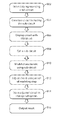
- FIG. 9 illustrates a flowchart of a method for simulating an RRAM cell according to an embodiment of the present invention.
- the present invention relates to simulation of Resistive Random-Access Memory (RRAM).
- RRAM Resistive Random-Access Memory
- SPICE Simulation Program with Integrated Circuit Emphasis
- FIG. 1 illustrates a simplified block diagram of an exemplary computer system 100 according to an embodiment of the present invention.
- Computer system 100 typically includes at least one processor 102 , which communicates with a number of peripheral devices via bus subsystem 104 .
- peripheral devices typically include a storage subsystem 114 , user interface input devices 110 , and a network interface subsystem 106 .
- the input and output devices allow user interaction with computer system 100 . It should be apparent that the user may be a human user, a device, a process, another computer, and the like.
- Network interface subsystem 106 provides an interface to outside networks.
- User interface input devices 110 may include a keyboard, pointing devices such as a mouse, trackball, touchpad, or graphics tablet, a scanner, a touchscreen incorporated into the display, audio input devices such as voice recognition systems, microphones, and other types of input devices.
- pointing devices such as a mouse, trackball, touchpad, or graphics tablet
- audio input devices such as voice recognition systems, microphones, and other types of input devices.
- use of the term “input device” is intended to include all possible types of devices and ways to input information into computer system 100 or onto communication network 108 .
- User interface output devices 112 may include a display subsystem, a printer, a fax machine, or non-visual displays such as audio output devices.
- the display subsystem may be a cathode ray tube (CRT), a flat-panel device such as a liquid crystal display (LCD), or a projection device.
- the display subsystem may also provide non-visual display such as via audio output devices.
- output device is intended to include all possible types of devices and ways to output information from computer system 100 to a user or to another machine or computer system.
- Storage subsystem 114 stores the basic programming and data constructs that provide the functionality of the computer system.
- the various modules implementing the functionality of the present invention may be stored in storage subsystem 114 . These software modules are generally executed by processor(s) 102 . In a distributed environment, the software modules may be stored on a plurality of computer systems and executed by processors of the plurality of computer systems.
- Storage subsystem 114 also provides a repository for storing the various databases storing information according to the present invention.
- Storage subsystem 114 typically comprises memory subsystem 116 and file storage subsystem 122 .
- Memory subsystem 116 typically includes a number of memories including a main random access memory (RAM) 120 for storage of instructions and data during program execution and a read only memory (ROM) 118 in which fixed instructions are stored.
- File storage subsystem 122 provides persistent (non-volatile) storage for program and data files, and may include a hard disk drive, a floppy disk drive along with associated removable media, a Compact Digital Read Only Memory (CD-ROM) drive, an optical drive, removable media cartridges, and other like storage media.
- One or more of the drives may be located at remote locations on other connected computers at another site on communication network 108 . Information stored according to the teachings of the present invention may also be stored by file storage subsystem 122 .
- Bus subsystem 104 provides a mechanism for letting the various components and subsystems of computer system 100 communicate with each other as intended.
- the various subsystems and components of computer system 100 need not be at the same physical location but may be distributed at various locations within a distributed network.
- bus subsystem 104 is shown schematically as a single bus, alternative embodiments of the bus subsystem may utilize multiple busses.
- Computer system 100 itself can be of varying types including a personal computer, a portable computer, a workstation, a computer terminal, a network computer, a mainframe, or any other data processing system. Due to the ever-changing nature of computers and networks, the description of computer system 100 depicted in FIG. 1 is intended only as a specific example for purposes of illustrating the preferred embodiment of the computer system. Many other configurations of a computer system are possible having more or fewer components than the computer system depicted in FIG. 1 . Client computer systems and server computer systems generally have the same configuration as shown in FIG. 1 , with the server systems generally having more storage capacity and computing power than the client systems.
- RRAM The electrical behavior of RRAM is complex, and in the case of two-terminal RRAM, may take place in multiple discrete phases during a write cycle. These include a length growth phase and a width growth phase. These phases have distinct characteristics which must be dealt with separately in order to accurately model RRAM behavior.
- the first stage of filament growth in an RRAM cell 200 is shown in FIG. 2 a .
- the length ‘l’ of a filament 202 which is the distance between filament front 206 and top electrode 204 , grows as ions from the top electrode 204 are oxidized and migrate along the applied electric field towards the bottom electrode 208 .
- the distance between top electrode 204 and bottom electrode 208 is represented as ‘h’.
- the velocity of the filament front can be derived as follows:
- V therm kT/q and d is the hopping site distance, or distance between impurities, ⁇ 0 is the material-dependent ion hop attempt frequency, U a is the activation energy, k is Boltzmann's constant in J/K, T is the temperature in Kelvin, q is the charge on an electron, and l is the filament length as shown in FIG. 2 a.
- Equation 1 for deriving filament length with respect to time is:
- Equation 2 is:
- the filament length/has reached a value such that the filament essentially touches the bottom electrode e.g. characterized by the conductance being equal to the conductance quantum (7:748 ⁇ 10 ⁇ 5 S), or the spacing between the filament front 206 and the bottom electrode 208 being equal to the lattice spacing of the metal ion
- vertical growth halts and the filament enters the second growth stage, characterized by the expansion of its width as shown in FIG. 4 .
- the growth of the filament's diameter or width or area can be modeled as the addition of conductive filaments in parallel with the first.
- Equation 2 can be used when modeling the width growth as well.
- the term h ⁇ l remains constant, so the second stage of growth is a simpler function of voltage.
- the width variable remains equal to zero, and so the RRAM cell current is determined solely by the tunneling junction formed between the conductive filament 202 and the bottom electrode 208 .
- Different models including direct tunneling, trap-assisted tunneling, Frenkel-Poole conduction, and linear or non-linear resistor models, can be used to describe the current between the filament 202 and the bottom electrode 208 .
- the I-V can be calculated using a tunneling model according to the following Equation 3: [Eq.
- ⁇ , ⁇ , ⁇ , ⁇ , ⁇ 1 , and ⁇ 2 are all positive-valued parameters determined by material properties such as the barrier height for a Schottky barrier and for tunneling, the depletion width in the Schottky barrier region, the effective tunneling distance in the conducting region, and interface effects. In practice they can be treated as fitting parameters and are independent of w.
- Equations 7 is useful for describing the width propagation phase of RRAM cell activity.
- Equation 7 describes the rate of change of the state variable representing width with respect to the applied voltage. It originates from Equation 3 but is no longer explicitly dependent on the state variables/or w since the existing conductive regions do not affect the formation of new conductive regions.
- the expression is further chosen such that (dw/dt) can be different at positive and negative biases ( ⁇ 1 ⁇ 2 ) to account for potential differences in the activation energies for forward and backward ion hopping, e.g. in the presence of a build-in field. Having asymmetric activation energies ( ⁇ 1 ⁇ 2 ) however is not essential in modeling. When ⁇ 1 ⁇ 2 Equation 7 becomes a simpler form of Sin h( ⁇ V).
- thermo effects can play an important role in determining the final resistance value after switching.
- An embodiment in a SPICE environment allows for the incorporation of temperature effects through the ‘temp_ coeff’ parameter, which serves as the heat capacity of the device in units K/W.
- FIG. 5 a shows a circuit 500 used in a simulation program, including a RRAM device 502 connected in series with a resistor 504 and voltage source V a .
- resistor 502 can be replaced with current-compliance, a diode, or a transistor.
- FIGS. 5 b to 5 d show the effects of a voltage sweep performed on RRAM device 502 in circuit 500 .
- FIG. 5 e shows a temperature profile over time in a cell according to the applied voltage over time shown in FIG. 5 f.
- SPICE code using Equation 2 and Equation 5 for an RRAM component was constructed, and is featured in Table 1 below. Because most SPICE simulation environments cannot handle equations such as Eq. 3 directly and do not allow for arbitrary internal mutable variables, floating node capacitors are used to store the state variables required by the model. Thus, voltage or other electrical properties act as a proxy for physical state variables.
- SPICE ‘.ic’ directive initial conditions can be imposed on the state variables. This allows the user to begin a simulation with cells in the ‘ON,’ or even intermediate states.
- FIGS. 6 a and 6 b illustrate the layout of sub-circuits corresponding to the code in Table 1.
- the code can be thought of as having two parts. The first part is described by earlier sections of code including parameter definitions and functions through the line “*State variables.” This portion of the code corresponds to the circuit illustrated in FIG. 6 a .
- the circuit has three node locations 602 , 604 , and 606 , corresponding to node 1 , node 2 , and node 3 , respectively.
- the sub-circuit 600 in FIG. 6 a correlates to an actual RRAM cell, such as the cell represented in FIG. 2 .
- node location 602 in FIG. 6 a corresponds to top electrode 204
- node location 604 corresponds to the filament front 206
- node 606 corresponds to bottom electrode 208 .
- Resistor 608 located between node 602 and node 604 , corresponds to the “Rmet” resistor in the Table 1 code, which represents the fixed parasitic resistance inside an RRAM cell.
- Variable resistor 610 represents the active region, or switching region, of an RRAM cell. Current is solved for this region of a cell using the “Bw” function in Table 1, which corresponds to Equation 5, and is a function of V length , V ⁇ width , input voltage, and temperature.
- Sub-circuit 612 comprises three nodes 614 , 616 , and 618 , corresponding to nodes “length,” “width,” and “temp” in Table 1, respectively.
- a fourth node 620 node 0 , is located at ground.
- the circuit has three capacitors 622 , 624 , and 626 , and three current sources 628 , 630 , and 632 , one for each of the state variables representing length, width, and temperature.
- the capacitors are represented by Clength, Cnum, and Ctemp in Table 1, while the current sources are represented by Blength, Bwidth, and Btemp.
- SPICE treats the internal state variables representing physical characteristics as voltages.
- the code in Table 1 shows a capacitor Ctemp, it is not necessary to have a capacitor for temperature in order to run a simulation using the Table in some embodiments.
- the simulation can be performed using components other than capacitors to perform derivative functions.
- the components may include a current or voltage source, inductor, resistor, transistor, diode, or a combination thereof.
- the voltages on the floating nodes control the filament (e.g. length and width) growth while the voltage dropped across the device controls the current output and temperature characteristics. Growth of length and width is accelerated by elevated temperatures.
- the filament growth is exponentially dependent on the applied electric field, reducing the voltage across the device has a large impact on the derivative of the conductance.
- the filament growth can be controllably stopped at a specific conductance determined by the series-resistor, a consequence of which is the ability to reliably store more than two values of data in a cell.
- FIG. 7 a shows how the final resistance state is controlled by the use of resistors of various values.
- the series resistance using, for example, a series of resistors, a diode, a MOS selector, or different current compliance.
- FIG. 7 a shows the final resistance state after applying 4.75V for 50 nanoseconds through a variable resistor at various resistor values.
- the RRAM simulation provided herein is particularly useful for capturing switching dynamics which may be hard to obtain using other, simpler simulations.
- the switching speed is not a constant for a given RRAM device, but rather is a sensitive function of the applied bias.
- ⁇ is an exponential function of the voltage applied across the device.
- FIG. 7 b shows the results of a model prediction, represented as a line, plotted against actual measured data, which is plotted as individual data points.
- FIG. 7 b demonstrates that the SPICE model's predicted switching times fit the switching times reported experimentally.
- the SPICE simulation of this embodiment shows that ⁇ is not dependent on the series resistance value.
- FIG. 8 shows a typical write-read sequence in an RRAM cell using programming and read pulses.
- the switching event 802 represented by a dotted line, is defined qualitatively as a substantial rise in current with a corresponding reduction in the voltage dropped across the device.
- the switching event 802 occurs at 36 ns.
- the device is probed using a voltage pulse with a magnitude much smaller (1 volt in this case) than that used for programming. Using the current through the circuit and the voltage dropped across the RRAM cell, a final resistance value can be calculated at a given read voltage.
- the final cell resistance values were found while varying the external series resistor 504 .
- the final resistance state varies linearly for series resistance values below 1M, with superlinear dependence above.
- the nonlinear dependence beyond 1M can be attributed to the elongation of a switching event, such that the device will not have fully switched when a very high series resistance is used.
- FIG. 9 A method for implementing an RRAM simulation according to an embodiment will be now described with respect to FIG. 9 .
- the embodiment is described as a simulation run in a SPICE environment, similar methods can be used in other simulation environments without departing from the scope and spirit of the invention.
- a simulation can be conducted in SPICE software, or other electronic simulation software that accepts programmable data to model the performance of components.
- a user enters data in step 902 , which includes data representing the electrical behavior of an RRAM cell.
- the data should include at least an equation representing filament length growth.
- the length growth equation is represented by Equation 2.
- Various embodiments can include various equations representing RRAM cell behavior, depending on the nature of the simulation and the desired level of accuracy.
- a highly accurate simulation can be made using Equation 2 to represent a length growth characteristic, Equation 7 to represent width growth, Equation 3 for tunneling current, equation 4 for areal expansion current, and a function such as the “temp_coeff” function in SPICE to represent thermal characteristics.
- An example of user data configured for SPICE is found in Table 1 above.
- the data entry step 902 may include data that assigns equations to represent electrical components to build a sub-circuit.
- the specific components may be selected according to a component's ability to accept the equations, such as the derivative with respect to time in Equation 3.
- the data in Table 1 uses floating capacitor nodes to store internal state variables.
- components including a current source, voltage source, capacitor, inductor, resistor, transistor, or diode, or a combination of these components or their equivalents, can be used to store state variables.
- the data may include initial conditions of variables in the simulated RRAM module, including conditions of filament length, filament width, and device temperature.
- initial conditions are specified using the “.ic” function in SPICE. Specifying initial conditions can be helpful for simulating various resistance states of a RRAM cell, or for specifying whether a cell is initially configured to be in an ‘ON’ or ‘OFF’ condition.
- the data is written to a memory as it is entered.
- the memory is located in the storage subsystem 114 shown in FIG. 1 , and can be in either the memory subsystem 116 or the file storage subsystem 122 .
- the memory can be portable, or stored remotely and accessed via a network.
- the memory should be non-transient, and accessible by a system that is configured to perform a simulation.
- Table 1 the data is entered so that the final data set represents a sub-circuit, which according to FIG. 6 comprises sub-circuits 600 and 612 .
- step 904 data is entered representing an electrical circuit including the sub-circuit from step 902 .
- the circuit can be simple as circuit 500 , or highly complex, involving a large number of memory cells. Circuits can be designed for many purposes including to simulate an actual product, to test a design principle, and to test the accuracy of a theory. One of skill in the art will recognize that there are virtually unlimited permutations of circuits that can be created to simulate various devices, properties, and conditions.
- step 902 is performed well in advance of subsequent simulation steps.
- Step 902 can be performed once for a plurality of subsequent simulations.
- SPICE can accept a simulated circuit in the form of a netlist.
- a single netlist can be prepared according to the above described methods and written to a memory, then recalled by the same or other users at later points in time to perform simulations.
- steps 902 can be performed contemporaneously with circuit generation 904 .
- a user can conduct a simulation using the simulated circuit to solve for various properties or conditions including current, voltage, resistance, temperature, filament length, or filament width at various points in time.
- a circuit including at least one RRAM cell is provided to the user in a display area of a computer system 100 so that the user can access data representing the circuit.
- the computer system calls the sub-circuit created in step 902 as a part of the circuit representing an RRAM cell.
- the circuit is then modeled using the computer system in step 910 .
- the modeling step includes performing a set of calculations using a processor 102 to model electrical and physical characteristics of the circuit.
- step 912 the circuit is adjusted using a result of the modeling step.
- the adjustment may be made as a result of changed conditions within the circuit including electrical, thermal, and physical properties, over time.
- the adjusted circuit is then stored in a storage subsystem 114 of computer system 100 .
- step 916 the system outputs the desired result to an output device 112 as shown in FIG. 1 , and/or stores the output on a memory in the memory subsystem 116 or the file storage subsystem 122 .
- Some of the outputs in the form of voltage may actually represent physical properties of the simulated RRAM cell, including temperature, area, and length.
- an additional step of converting values may be required, or performed as part of the modeling.
- the embodiment presented herein provides an accurate, physical model of an RRAM cell that can be used to simulate these novel devices and their interaction with other elements in a circuit. An emphasis was placed on describing the transient dynamics of the device so that its behavior during the switching event is captured. The important current characteristics are categorized into two phases corresponding to filament growth in length and width.
- the present invention has been described using selected embodiments. However, the invention may be modified without departing from the scope and spirit thereof.
- the modeling techniques can be applied to represent various types of RRAM devices including those based on metal oxide, chalcogenide based, and organic materials.
- modeling techniques described herein may be used with circuit simulation software programs other than SPICE, on a dedicated apparatus, or through any other means for simulating or predicting RRAM behavior.
Abstract
Description
Where Vtherm=kT/q and
d is the hopping site distance, or distance between impurities,
τ0 is the material-dependent ion hop attempt frequency,
Ua is the activation energy,
k is Boltzmann's constant in J/K,
T is the temperature in Kelvin,
q is the charge on an electron, and
l is the filament length as shown in
where Vd is the voltage dropped between each hopping site.
where h is distance between electrodes as shown in
leads to
[Eq. 3]
I Tunneling=sin V·Area·J 0·(P qexp(−A√{square root over (P q)}exp(P q +q|V|)exp(−A√{square root over (P q +q|V|)})) (3)
where
and
Pq is the average barrier height,
h is the distance between electrodes,
l is the length of the conductive filament,
q is the charge on an electron,
Area is the area of the end of a filament,
h0 is Plank's constant, and
m is the mass of an electron.
[Eq. 4]
I width =V·width·G 0 (4)
where the variable width represents a number of filaments, and G0 is the conductance through a single filament, which is normally constant for a given material. The total current consists of the sum of the two conduction regimes (
[Eq. 5]
I=I Tunneling +I Width (5)
[Eq. 6]
I width=(1−w)α[1−exp(−βV)]+wγ sin h(δV) (6)
The two conduction channels are in parallel and their relative weight is determined by the internal state variable w, which is the normalized area index representing the conductive region, i.e. w=0 indicates fully Schottky-dominated conduction, while w=1 indicates fully tunneling-dominated conduction. α, β, γ, δ, η1, and η2 are all positive-valued parameters determined by material properties such as the barrier height for a Schottky barrier and for tunneling, the depletion width in the Schottky barrier region, the effective tunneling distance in the conducting region, and interface effects. In practice they can be treated as fitting parameters and are independent of w.
Equation 7 describes the rate of change of the state variable representing width with respect to the applied voltage. It originates from
| TABLE 1 |
| SPICE code listing for a two-terminal RRAM device |
| *Parameters: |
| *to is hopping attempt frequency |
| *area is device area |
| *d is site hopping distance |
| *w is device length |
| *Ua is ion barrier height |
| *P is electron barrier height |
| .subckt memristor 3 1 params: |
| + to=4e12 area=1e−16 d=1-9 Ua=0.87 w=2.29e−9 P=.31 Rfil=100 |
| *Notes: |
| ************************************************************ |
| *In any function where k is a parameter, k is simply a dummy |
| variable, always called with 0 and not |
| *used in the function. A function was simply used for clarity. |
| ************************************************************ |
| .param k=1.38e−23 ;Boltzman's Constant |
| .param echarge=1.6021e−19 ;Charge on electron |
| .param temp_coeff=3e5 ;Specific Heat of Silver |
| .param th_conduct=0 ; |
| .param plank = {6.62606e−34} ;Plank's Constant |
| .param Pq={P*echarge} ;Electron Barrier Height |
| .param m={0.09*9.109e−31} ;effective mass of an electron |
| .param lamda=0.03 a1=2.1 a2=2.3 |
| .param nnor=1e−9 |
| .param cpac={1} |
| .func T(z) 300 + temp_coeff*V(1,3)*I(Rmet) |
| .func Vthermal(z) {k*T(0)/echarge} |
| Rmet 1 2 {Rfil} |
| *Current Output: |
| .func A(z) {4*Pi*(w−cpac*V(length))*sqrt(2*m)/plank} |
| .func Jo(z) {echarge/(2*Pi*plank*(w−cpac*V(length))**2)} |
| .func J_tun(z) {sgn(V(2,3))*area*Jo(0)*(Pq*exp(−(0)*sqrt(Pq))− |
| (Pq+echarge*abs(V(2,3)))*exp(−A(0)*sqrt |
| (Pq+echarge*abs(V(2,3)))))} |
| Bw 2 3 I=J_tun (0) + V(2,3)*(V(width))*(77e−6) |
| *State variables: |
| Clength length 0 1 |
| Cwidth width 0 1 |
| Ctemp temp 0 1 |
| *Initial Conditions: |
| .ic V(length) = .1e−12 |
| .ic V(width) = 0 |
| .ic V(temp) = 300 |
| *Supplementary Functions: |
| .func Vo(z) 2*Vthermal(0)*(w−cpac*V(length))/d |
| .func ion_flow(z) { d*to*exp(− |
| Ua/Vthermal(0))*(exp(V(2,3)/Vo(0))−exp(−V(2,3)/Vo(0))) } |
| .func prev_underfloor(z) {u( sgn(cpac*V(length)−1e−12) + |
| sgn(ion_flow(0)) + 1 ) } |
| .func single_growth(z) {u(77e−6 − J_tun(0)/V(2,3))*(V(2,3)>=0) |
| + (V(2,3)<0)*(V(width)<=0)} |
| *State Variable Derivatives: |
| Blength 0 length I=single_growth(0)*prev_underflow(0) |
| *ion_flow(0) |
| Bwidth 0 width I=(1−single_growth(0))*ion_flow(0)/V(length) |
| Btemp 0 temp I=temp_coeff*V(1,3)*I(Rmet) |
| .ends memristor |
Claims (14)
Priority Applications (1)
| Application Number | Priority Date | Filing Date | Title |
|---|---|---|---|
| US13/077,941 US8930174B2 (en) | 2010-12-28 | 2011-03-31 | Modeling technique for resistive random access memory (RRAM) cells |
Applications Claiming Priority (2)
| Application Number | Priority Date | Filing Date | Title |
|---|---|---|---|
| US201061427741P | 2010-12-28 | 2010-12-28 | |
| US13/077,941 US8930174B2 (en) | 2010-12-28 | 2011-03-31 | Modeling technique for resistive random access memory (RRAM) cells |
Publications (2)
| Publication Number | Publication Date |
|---|---|
| US20120166169A1 US20120166169A1 (en) | 2012-06-28 |
| US8930174B2 true US8930174B2 (en) | 2015-01-06 |
Family
ID=46318128
Family Applications (1)
| Application Number | Title | Priority Date | Filing Date |
|---|---|---|---|
| US13/077,941 Active 2032-09-14 US8930174B2 (en) | 2010-12-28 | 2011-03-31 | Modeling technique for resistive random access memory (RRAM) cells |
Country Status (1)
| Country | Link |
|---|---|
| US (1) | US8930174B2 (en) |
Cited By (3)
| Publication number | Priority date | Publication date | Assignee | Title |
|---|---|---|---|---|
| US9246087B1 (en) * | 2014-11-24 | 2016-01-26 | Intermolecular, Inc. | Electron barrier height controlled interfaces of resistive switching layers in resistive random access memory cells |
| US10903421B2 (en) | 2018-10-01 | 2021-01-26 | International Business Machines Corporation | Controlling filament formation and location in a resistive random-access memory device |
| US11417412B1 (en) | 2021-03-01 | 2022-08-16 | United Microelectronics Corp. | Cell trace circuit for measuring I-V property of memory cell |
Families Citing this family (3)
| Publication number | Priority date | Publication date | Assignee | Title |
|---|---|---|---|---|
| US9911788B2 (en) | 2014-05-05 | 2018-03-06 | Hewlett Packard Enterprise Development Lp | Selectors with oxide-based layers |
| WO2017105460A1 (en) * | 2015-12-17 | 2017-06-22 | Hewlett Packard Enterprise Development Lp | Improved computational accuracy in a crossbar array |
| SG10201606137YA (en) | 2016-07-26 | 2018-02-27 | Silicon Storage Tech Inc | Current forming of resistive random access memory (rram) cell filament |
Citations (211)
| Publication number | Priority date | Publication date | Assignee | Title |
|---|---|---|---|---|
| US680652A (en) | 1897-11-08 | 1901-08-13 | Leonard L Elden | Circuit-breaker. |
| US4433468A (en) | 1980-03-26 | 1984-02-28 | Nippon Electric Co., Ltd. | Method for making semiconductor device having improved thermal stress characteristics |
| US4684972A (en) | 1981-08-07 | 1987-08-04 | The British Petroleum Company, P.L.C. | Non-volatile amorphous semiconductor memory device utilizing a forming voltage |
| US4741601A (en) | 1984-10-08 | 1988-05-03 | Nec Corporation | Non-linear device for driving liquid crystal display |
| US5139911A (en) | 1989-01-04 | 1992-08-18 | Fuji Xerox Co., Ltd. | Electrophotographic photoreceptor with two part surface layer |
| US5242855A (en) | 1991-09-30 | 1993-09-07 | Nec Corporation | Method of fabricating a polycrystalline silicon film having a reduced resistivity |
| US5278085A (en) | 1992-08-11 | 1994-01-11 | Micron Semiconductor, Inc. | Single mask process for forming both n-type and p-type gates in a polycrystalline silicon layer during the formation of a semiconductor device |
| US5315131A (en) | 1990-11-22 | 1994-05-24 | Matsushita Electric Industrial Co., Ltd. | Electrically reprogrammable nonvolatile memory device |
| US5335219A (en) | 1991-01-18 | 1994-08-02 | Ovshinsky Stanford R | Homogeneous composition of microcrystalline semiconductor material, semiconductor devices and directly overwritable memory elements fabricated therefrom, and arrays fabricated from the memory elements |
| US5360981A (en) | 1989-05-11 | 1994-11-01 | British Telecommunications Public Limited Company | Amorphous silicon memory |
| US5457649A (en) | 1994-08-26 | 1995-10-10 | Microchip Technology, Inc. | Semiconductor memory device and write-once, read-only semiconductor memory array using amorphous-silicon and method therefor |
| US5538564A (en) | 1994-03-18 | 1996-07-23 | Regents Of The University Of California | Three dimensional amorphous silicon/microcrystalline silicon solar cells |
| US5541869A (en) | 1991-10-22 | 1996-07-30 | British Telecommunications, Plc | Resistive memory element |
| US5594363A (en) | 1995-04-07 | 1997-01-14 | Zycad Corporation | Logic cell and routing architecture in a field programmable gate array |
| US5614756A (en) | 1990-04-12 | 1997-03-25 | Actel Corporation | Metal-to-metal antifuse with conductive |
| US5751012A (en) | 1995-06-07 | 1998-05-12 | Micron Technology, Inc. | Polysilicon pillar diode for use in a non-volatile memory cell |
| US5840608A (en) | 1996-11-22 | 1998-11-24 | United Microelectronics Corporation | High density ROM and a method of making the same |
| US5970332A (en) | 1995-03-28 | 1999-10-19 | U.S. Philips Corporation | Method of manufacturing a semiconductor device with a BiCMOS circuit |
| US5998244A (en) | 1996-08-22 | 1999-12-07 | Micron Technology, Inc. | Memory cell incorporating a chalcogenide element and method of making same |
| US6122318A (en) | 1996-10-31 | 2000-09-19 | Kabushiki Kaisha Toshiba | Video encoding apparatus and video decoding apparatus |
| US6128214A (en) | 1999-03-29 | 2000-10-03 | Hewlett-Packard | Molecular wire crossbar memory |
| US6143642A (en) | 1997-12-22 | 2000-11-07 | Vlsi Technology, Inc. | Programmable semiconductor structures and methods for making the same |
| US6180998B1 (en) | 1998-03-30 | 2001-01-30 | Lsi Logic Corporation | DRAM with built-in noise protection |
| US6259116B1 (en) | 1997-10-22 | 2001-07-10 | U.S. Philips Corporation | Multiple memory element semiconductor memory devices |
| US6291836B1 (en) | 1996-06-05 | 2001-09-18 | U. S. Philips Corporation | Method of operating a programmable, non-volatile memory device |
| US6436765B1 (en) | 2001-02-09 | 2002-08-20 | United Microelectronics Corp. | Method of fabricating a trenched flash memory cell |
| US6436818B1 (en) | 1997-02-19 | 2002-08-20 | Micron Technology, Inc. | Semiconductor structure having a doped conductive layer |
| US6492694B2 (en) | 1998-02-27 | 2002-12-10 | Micron Technology, Inc. | Highly conductive composite polysilicon gate for CMOS integrated circuits |
| WO2003034498A1 (en) | 2001-10-16 | 2003-04-24 | Midwest Research Institute | Stacked switchable element and diode combination |
| US20030174574A1 (en) | 2002-03-12 | 2003-09-18 | Perner Frederick A. | Write pulse circuit for a magnetic memory |
| US6627530B2 (en) | 2000-12-22 | 2003-09-30 | Matrix Semiconductor, Inc. | Patterning three dimensional structures |
| US20030206659A1 (en) | 1998-09-08 | 2003-11-06 | Canon Kabushiki Kaisha | Image processing apparatus including an image data encoder having at least two scalability modes and method therefor |
| US20040026682A1 (en) | 2002-06-17 | 2004-02-12 | Hai Jiang | Nano-dot memory and fabricating same |
| US6762474B1 (en) * | 1998-06-10 | 2004-07-13 | Agere Systems Inc. | Method and apparatus for temperature compensation of read-only memory |
| US6768157B2 (en) | 2001-08-13 | 2004-07-27 | Advanced Micro Devices, Inc. | Memory device |
| US20040170040A1 (en) | 2002-08-02 | 2004-09-02 | Unity Semiconductor Corporation | Rewritable memory with non-linear memory element |
| US6815286B2 (en) | 2001-08-13 | 2004-11-09 | Advanced Micro Devices, Inc. | Memory device |
| US6838720B2 (en) | 2001-08-13 | 2005-01-04 | Advanced Micro Devices, Inc. | Memory device with active passive layers |
| US6848012B2 (en) | 2002-09-27 | 2005-01-25 | Broadcom Corporation | Method and system for an adaptive multimode media queue |
| US20050020510A1 (en) | 2002-08-29 | 2005-01-27 | Benedict Dale L. | D-mannose contraceptives |
| US20050029587A1 (en) | 1995-06-07 | 2005-02-10 | Harshfield Steven T. | Method and apparatus for forming an integrated circuit electrode having a reduced contact area |
| US6858482B2 (en) | 2002-04-10 | 2005-02-22 | Micron Technology, Inc. | Method of manufacture of programmable switching circuits and memory cells employing a glass layer |
| US6858481B2 (en) | 2001-08-13 | 2005-02-22 | Advanced Micro Devices, Inc. | Memory device with active and passive layers |
| US20050041498A1 (en) | 2003-06-16 | 2005-02-24 | Claudio Resta | Writing circuit for a phase change memory device |
| US6864127B2 (en) | 1997-04-25 | 2005-03-08 | Semiconductor Energy Laboratory Co., Ltd. | Semiconductor device and method of fabricating the same |
| US20050052915A1 (en) | 2002-12-19 | 2005-03-10 | Matrix Semiconductor, Inc. | Nonvolatile memory cell without a dielectric antifuse having high- and low-impedance states |
| US20050062045A1 (en) | 2002-10-02 | 2005-03-24 | Arup Bhattacharyya | Processes of forming stacked resistor constructions |
| US20050073881A1 (en) | 2003-10-06 | 2005-04-07 | Tran Lung The | Magnetic memory device including groups of series-connected memory elements |
| US6881994B2 (en) | 2000-08-14 | 2005-04-19 | Matrix Semiconductor, Inc. | Monolithic three dimensional array of charge storage devices containing a planarized surface |
| US6927430B2 (en) | 2001-06-28 | 2005-08-09 | Sharp Laboratories Of America, Inc. | Shared bit line cross-point memory array incorporating P/N junctions |
| US20050175099A1 (en) | 2004-02-06 | 2005-08-11 | Nokia Corporation | Transcoder and associated system, method and computer program product for low-complexity reduced resolution transcoding |
| US6939787B2 (en) | 1999-12-28 | 2005-09-06 | Fujitsu Limited | Method for fabricating semiconductor device having gate electrode with polymetal structure of polycrystalline silicon film and metal film |
| US6946719B2 (en) | 2003-12-03 | 2005-09-20 | Matrix Semiconductor, Inc | Semiconductor device including junction diode contacting contact-antifuse unit comprising silicide |
| US20060017488A1 (en) | 2004-07-21 | 2006-01-26 | Sharp Laboratories Of America, Inc. | Mono-polarity switchable PCMO resistor trimmer |
| US7020006B2 (en) | 2002-08-02 | 2006-03-28 | Unity Semiconductor Corporation | Discharge of conductive array lines in fast memory |
| US7023093B2 (en) | 2002-10-24 | 2006-04-04 | International Business Machines Corporation | Very low effective dielectric constant interconnect Structures and methods for fabricating the same |
| US7102150B2 (en) | 2001-05-11 | 2006-09-05 | Harshfield Steven T | PCRAM memory cell and method of making same |
| US7122853B1 (en) | 2004-08-17 | 2006-10-17 | Fasl, Inc. | Method to improve yield and simplify operation of polymer memory cells |
| US20060281244A1 (en) | 2005-06-08 | 2006-12-14 | Masayuki Ichige | Nonvolatile semiconductor memory device and method of manufacturing the same |
| US20070008773A1 (en) | 2005-07-11 | 2007-01-11 | Matrix Semiconductor, Inc. | Nonvolatile memory cell comprising switchable resistor and transistor |
| US20070015348A1 (en) | 2005-07-18 | 2007-01-18 | Sharp Laboratories Of America, Inc. | Crosspoint resistor memory device with back-to-back Schottky diodes |
| US20070045615A1 (en) | 2005-08-31 | 2007-03-01 | Samsung Electronics Co., Ltd. | Non-volatile organic resistance random access memory device and method of manufacturing the same |
| US7187577B1 (en) | 2005-11-23 | 2007-03-06 | Grandis, Inc. | Method and system for providing current balanced writing for memory cells and magnetic devices |
| US20070087508A1 (en) | 2003-12-03 | 2007-04-19 | Herner S B | Method for making a p-i-n diode crystallized adjacent to a silicide in series with a dielectric antifuse |
| US20070091685A1 (en) | 2004-01-27 | 2007-04-26 | Guterman Daniel C | Efficient verification for coarse/fine programming of non-volatile memory |
| US20070090425A1 (en) | 2005-09-28 | 2007-04-26 | Matrix Semiconductor, Inc. | Memory cell comprising switchable semiconductor memory element with trimmable resistance |
| US20070105390A1 (en) | 2005-11-09 | 2007-05-10 | Oh Travis B | Oxygen depleted etching process |
| US20070105284A1 (en) | 2003-12-03 | 2007-05-10 | Herner S B | Method for forming a memory cell comprising a semiconductor junction diode crystallized adjacent to a silicide |
| US7221599B1 (en) | 2004-11-01 | 2007-05-22 | Spansion, Llc | Polymer memory cell operation |
| US7238607B2 (en) | 2002-12-19 | 2007-07-03 | Sandisk 3D Llc | Method to minimize formation of recess at surface planarized by chemical mechanical planarization |
| US20070205510A1 (en) | 2006-03-03 | 2007-09-06 | Lavoie Adrien R | Noble metal barrier layers |
| US20070228414A1 (en) | 2006-03-31 | 2007-10-04 | Sandisk 3D, Llc | Heterojunction device comprising a semiconductor and a resistivity-switching oxide or nitride |
| JP2007281208A (en) | 2006-04-07 | 2007-10-25 | Matsushita Electric Ind Co Ltd | Multilayer resistance variable element array, resistance variable device, multilayer nonvolatile storage element array, and nonvolatile storage device |
| US7289353B2 (en) | 2004-08-17 | 2007-10-30 | Spansion, Llc | Systems and methods for adjusting programming thresholds of polymer memory cells |
| US20070284575A1 (en) | 2005-07-18 | 2007-12-13 | Sharp Laboratories Of America, Inc. | Metal/semiconductor/metal current limiter |
| US20070291527A1 (en) | 2006-06-07 | 2007-12-20 | Sony Corporation | Memory apparatus |
| US20070290186A1 (en) | 2006-05-04 | 2007-12-20 | El Mostafa Bourim | Non-volatile variable resistance memory device and method of fabricating the same |
| US20070297501A1 (en) | 2006-06-08 | 2007-12-27 | Via Technologies, Inc. | Decoding Systems and Methods in Computational Core of Programmable Graphics Processing Unit |
| US20070295950A1 (en) | 2006-06-27 | 2007-12-27 | Samsung Electronics Co., Ltd. | Variable resistance random access memory device and a method of fabricating the same |
| US20080002481A1 (en) | 2002-12-20 | 2008-01-03 | Dietmar Gogl | Integrated Circuit, Method of Operating an Integrated Circuit, Method of Manufacturing an Integrated Circuit, Memory Module, Stackable Memory Module |
| US20080006907A1 (en) | 2006-07-06 | 2008-01-10 | Samsung Electronics Co., Ltd | Non-volatile memory device including a variable resistance material |
| US7324363B2 (en) * | 2005-12-12 | 2008-01-29 | Synopsys, Inc. | SPICE optimized for arrays |
| US20080048164A1 (en) | 2006-07-11 | 2008-02-28 | Matsushita Electric Industrial Co., Ltd. | Electro-resistance element, method of manufacturing the same and electro-resistance memory using the same |
| US20080090337A1 (en) | 2006-10-03 | 2008-04-17 | Williams R Stanley | Electrically actuated switch |
| US20080089110A1 (en) | 2006-10-16 | 2008-04-17 | Warren Robinett | Crossbar-memory systems and methods for writing to and reading from crossbar memory junctions of crossbar-memory systems |
| US7365411B2 (en) | 2004-08-12 | 2008-04-29 | Micron Technology, Inc. | Resistance variable memory with temperature tolerant materials |
| US20080106926A1 (en) | 2006-11-08 | 2008-05-08 | Symetrix Corporation | Non-volatile resistance switching memories and methods of making same |
| US20080106925A1 (en) | 2006-11-08 | 2008-05-08 | Symetrix Corporation | Correlated electron memory |
| US7405418B2 (en) | 2004-02-17 | 2008-07-29 | Infineon Technologies Ag | Memory device electrode with a surface structure |
| US20080185567A1 (en) | 2007-02-05 | 2008-08-07 | Nitin Kumar | Methods for forming resistive switching memory elements |
| US20080198934A1 (en) | 2007-02-20 | 2008-08-21 | Edward Hong | Motion refinement engine for use in video encoding in accordance with a plurality of sub-pixel resolutions and methods for use therewith |
| US20080206931A1 (en) | 2002-07-26 | 2008-08-28 | Laurent Breuil | Nonvolatile memory element and production method thereof and storage memory arrangement |
| US20080205179A1 (en) | 2007-02-28 | 2008-08-28 | Qimonda Ag | Integrated circuit having a memory array |
| US20080220601A1 (en) | 2007-03-05 | 2008-09-11 | Nitin Kumar | Methods for forming nonvolatile memory elements with resistive-switching metal oxides |
| US20080232160A1 (en) | 2007-02-27 | 2008-09-25 | International Business Machines Corporation | Rectifying element for a crosspoint based memory array architecture |
| US20080278990A1 (en) | 2007-05-09 | 2008-11-13 | Pragati Kumar | Resistive-switching nonvolatile memory elements |
| US20080304312A1 (en) * | 2007-06-11 | 2008-12-11 | Macronix International Co., Ltd. | Resistance memory with tungsten compound and manufacturing |
| US20080311722A1 (en) | 2007-06-15 | 2008-12-18 | Sandisk 3D Llc | Method for forming polycrystalline thin film bipolar transistors |
| US20090001345A1 (en) | 2007-06-29 | 2009-01-01 | April Schricker | Memory cell that employs a selectively deposited reversible resistance-switching element and methods of forming the same |
| US20090003717A1 (en) | 2007-06-28 | 2009-01-01 | Mitsubishi Electric Corporation | Image encoding device, image decoding device, image encoding method and image decoding method |
| US7474000B2 (en) | 2003-12-05 | 2009-01-06 | Sandisk 3D Llc | High density contact to relaxed geometry layers |
| WO2009005699A1 (en) | 2007-06-29 | 2009-01-08 | Sandisk 3D, Llc | Memory cell that employs a selectively grown reversible resistance-switching element and methods of forming the same |
| US20090014707A1 (en) | 2006-10-20 | 2009-01-15 | Wei Lu | Non-volatile solid state resistive switching devices |
| US20090052226A1 (en) | 2007-08-24 | 2009-02-26 | Samsung Electronics Co., Ltd | Resistive random access memory device |
| US20090095951A1 (en) | 2007-10-12 | 2009-04-16 | Ovonyx, Inc. | Memory Device With Low Reset Current |
| US7521705B2 (en) | 2005-08-15 | 2009-04-21 | Micron Technology, Inc. | Reproducible resistance variable insulating memory devices having a shaped bottom electrode |
| US7534625B2 (en) | 2004-09-24 | 2009-05-19 | Karpov Ilya V | Phase change memory with damascene memory element |
| US7541252B2 (en) | 2006-11-09 | 2009-06-02 | Samsung Electronics Co., Ltd. | Methods of fabricating a semiconductor device including a self-aligned cell diode |
| US20090152737A1 (en) | 2000-07-14 | 2009-06-18 | Micron Technology, Inc. | Memory devices having contact features |
| US7550380B2 (en) | 2004-11-03 | 2009-06-23 | Micron Technology, Inc. | Electroless plating of metal caps for chalcogenide-based memory devices |
| US20090168486A1 (en) | 2007-12-27 | 2009-07-02 | Sandisk 3D Llc | Large capacity one-time programmable memory cell using metal oxides |
| US20090231910A1 (en) | 2008-03-11 | 2009-09-17 | Micron Technology, Inc. | Non-volatile memory with resistive access component |
| US20090250787A1 (en) | 2008-04-07 | 2009-10-08 | Toshie Kutsunai | Semiconductor storage device and manufacturing method of the same |
| US20090257265A1 (en) | 2008-04-11 | 2009-10-15 | Sandisk 3D Llc | Multilevel nonvolatile memory device containing a carbon storage material and methods of making and using same |
| US20090256130A1 (en) | 2008-04-11 | 2009-10-15 | Sandisk 3D Llc | Memory cell that employs a selectively fabricated carbon nano-tube reversible resistance-switching element, and methods of forming the same |
| US7606059B2 (en) | 2003-03-18 | 2009-10-20 | Kabushiki Kaisha Toshiba | Three-dimensional programmable resistance memory device with a read/write circuit stacked under a memory cell array |
| US20090267047A1 (en) | 2008-04-28 | 2009-10-29 | Hitachi, Ltd. | Semiconductor memory device and manufacturing method thereof |
| US7615439B1 (en) | 2008-09-29 | 2009-11-10 | Sandisk Corporation | Damascene process for carbon memory element with MIIM diode |
| US20090298224A1 (en) | 2002-12-13 | 2009-12-03 | Lowrey Tyler A | Memory and Access Device and Method Therefor |
| US20090321789A1 (en) | 2008-06-30 | 2009-12-31 | Sandisk 3D Llc | Triangle two dimensional complementary patterning of pillars |
| US20100007937A1 (en) | 2006-11-09 | 2010-01-14 | Sage Electrochromics, Inc. | Method of making an ion-switching device without a separate lithiation step |
| US20100012914A1 (en) | 2008-07-18 | 2010-01-21 | Sandisk 3D Llc | Carbon-based resistivity-switching materials and methods of forming the same |
| US20100019310A1 (en) | 2008-07-25 | 2010-01-28 | Kabushiki Kaisha Toshiba | Semiconductor memory device |
| US20100019221A1 (en) | 2008-07-22 | 2010-01-28 | Macronix International Co., Ltd. | Fully self-aligned pore-type memory cell having diode access device |
| US20100034518A1 (en) | 2003-11-10 | 2010-02-11 | Panasonic Corporation | Integrated circuit for use in a playback apparatus |
| US20100032638A1 (en) | 2008-08-07 | 2010-02-11 | Sandisk 3D Llc | Memory cell that includes a carbon-based memory element and methods of forming the same |
| US20100046622A1 (en) | 2006-12-14 | 2010-02-25 | Thomson Licensing | Method and apparatus for encoding and/or decoding bit depth scalable video data using adaptive enhancement layer residual prediction |
| US20100044708A1 (en) | 2008-08-19 | 2010-02-25 | Chunghwa Picture Tubes, Ltd. | Thin film transistor, pixel structure and fabrication methods thereof |
| US20100085798A1 (en) | 2008-10-08 | 2010-04-08 | The Regents Of The University Of Michigan | Silicon-based nanoscale resistive device with adjustable resistance |
| US20100084625A1 (en) | 2008-10-02 | 2010-04-08 | Guy Wicker | Memory Device |
| US20100090192A1 (en) | 2006-08-31 | 2010-04-15 | Nxp, B.V. | Method for controlled formation of the resistive switching material in a resistive switching device and device obtained thereof |
| US20100101290A1 (en) | 2008-10-24 | 2010-04-29 | Antonio Bertolotto | Method for the production of an agent for treatment of agricultural soils |
| US20100102290A1 (en) | 2008-10-20 | 2010-04-29 | The Regents Of The University Of Michigan | Silicon based nanoscale crossbar memory |
| US7728318B2 (en) | 2006-11-16 | 2010-06-01 | Sandisk Corporation | Nonvolatile phase change memory cell having a reduced contact area |
| US7729158B2 (en) | 2003-04-03 | 2010-06-01 | Kabushiki Kaisha Toshiba | Resistance change memory device |
| US20100157710A1 (en) | 2008-12-19 | 2010-06-24 | Unity Semiconductor Corporation | Array Operation Using A Schottky Diode As a Non-Ohmic Isolation Device |
| US20100157651A1 (en) | 2008-12-18 | 2010-06-24 | Sandisk 3D Llc | Method of programming a nonvolatile memory device containing a carbon storage material |
| US20100163828A1 (en) | 2008-12-30 | 2010-07-01 | Industrial Technology Research Institute | Phase change memory devices and methods for fabricating the same |
| US7749805B2 (en) | 2005-03-10 | 2010-07-06 | Qimonda Ag | Method for manufacturing an integrated circuit including an electrolyte material layer |
| US20100176368A1 (en) | 2009-01-14 | 2010-07-15 | Ko Nikka | Method of manufacturing semiconductor memory device, and semiconductor memory device |
| US7772581B2 (en) | 2006-09-11 | 2010-08-10 | Macronix International Co., Ltd. | Memory device having wide area phase change element and small electrode contact area |
| US7786589B2 (en) | 2006-12-06 | 2010-08-31 | Kabushiki Kaisha Toshiba | Semiconductor device and method for manufacturing semiconductor device |
| US7786464B2 (en) | 2007-11-20 | 2010-08-31 | Infineon Technologies Ag | Integrated circuit having dielectric layer including nanocrystals |
| US20100219510A1 (en) | 2008-06-30 | 2010-09-02 | Sandisk 3D Llc | Method for fabricating high density pillar structures by double patterning using positive photoresist |
| US20100221868A1 (en) | 2007-12-04 | 2010-09-02 | Regino Sandoval | Active Material Devices with Containment Layer |
| US7824956B2 (en) | 2007-06-29 | 2010-11-02 | Sandisk 3D Llc | Memory cell that employs a selectively grown reversible resistance-switching element and methods of forming the same |
| US7829875B2 (en) | 2006-03-31 | 2010-11-09 | Sandisk 3D Llc | Nonvolatile rewritable memory cell comprising a resistivity-switching oxide or nitride and an antifuse |
| US7835170B2 (en) | 2005-05-09 | 2010-11-16 | Nantero, Inc. | Memory elements and cross point switches and arrays of same using nonvolatile nanotube blocks |
| US20100321095A1 (en) | 2008-06-10 | 2010-12-23 | Takumi Mikawa | Semiconductor device, manufacturing method of semiconductor device, semiconductor chip and system |
| US7859884B2 (en) | 2005-01-19 | 2010-12-28 | Sandisk 3D Llc | Structure and method for biasing phase change memory array for reliable writing |
| US20110006275A1 (en) | 2009-07-13 | 2011-01-13 | Seagate Technology Llc | Non-volatile resistive sense memory |
| US7881097B2 (en) | 2006-12-26 | 2011-02-01 | Sony Corporation | Storage element and memory |
| KR20110014248A (en) | 2010-11-28 | 2011-02-10 | 오세영 | A driver to set up lighting slab at night throngh solar panel |
| US7897953B2 (en) | 2008-01-16 | 2011-03-01 | Micron Technology, Inc. | Multi-level programmable PCRAM memory |
| US7898838B2 (en) | 2008-10-31 | 2011-03-01 | Seagate Technology Llc | Resistive sense memory calibration for self-reference read method |
| US7920412B2 (en) | 2006-09-29 | 2011-04-05 | Kabushiki Kaisha Toshiba | Magnetic random access memory and method of manufacturing the same |
| US7924138B2 (en) | 2007-03-01 | 2011-04-12 | Fujitsu Limited | Semiconductor device and manufacturing method of the same |
| US20110089391A1 (en) | 2009-10-20 | 2011-04-21 | Andrei Mihnea | Punch-through diode steering element |
| US20110133149A1 (en) | 2009-12-04 | 2011-06-09 | Sonehara Takeshi | Resistance change memory and manufacturing method thereof |
| US20110136327A1 (en) | 2009-12-03 | 2011-06-09 | Applied Materials, Inc. | High mobility monolithic p-i-n diodes |
| US7968419B2 (en) | 2005-07-18 | 2011-06-28 | Sharp Laboratories Of America, Inc. | Back-to-back metal/semiconductor/metal (MSM) Schottky diode |
| US20110155991A1 (en) | 2009-12-29 | 2011-06-30 | Industrial Technology Research Institute | Resistive memory device and fabricating method thereof |
| US20110194329A1 (en) | 2010-02-09 | 2011-08-11 | Sony Corporation | Memory component, memory device, and method of operating memory device |
| US20110198557A1 (en) | 2008-02-07 | 2011-08-18 | International Business Machines Corporation | Method for fabrication of crystalline diodes for resistive memories |
| US8004882B2 (en) | 2004-06-04 | 2011-08-23 | Micron Technology, Inc. | Spintronic devices with integrated transistors |
| US20110204312A1 (en) | 2008-05-10 | 2011-08-25 | Intermolecular, Inc. | Confinement techniques for non-volatile resistive-switching memories |
| US20110205782A1 (en) | 2010-02-23 | 2011-08-25 | Xiying Chen Costa | Step soft program for reversible resistivity-switching elements |
| US20110212616A1 (en) | 2010-02-26 | 2011-09-01 | Robert Seidel | Metallization system of a semiconductor device comprising rounded interconnects formed by hard mask rounding |
| US8018760B2 (en) | 2006-12-28 | 2011-09-13 | Panasonic Corporation | Resistance variable element and resistance variable memory apparatus |
| US8021897B2 (en) | 2009-02-19 | 2011-09-20 | Micron Technology, Inc. | Methods of fabricating a cross point memory array |
| US20110227028A1 (en) | 2010-03-16 | 2011-09-22 | Deepak Chandra Sekar | Bottom electrodes for use with metal oxide resistivity switching layers |
| US8045364B2 (en) | 2009-12-18 | 2011-10-25 | Unity Semiconductor Corporation | Non-volatile memory device ion barrier |
| US8054674B2 (en) | 2007-05-10 | 2011-11-08 | Sharp Kabushiki Kaisha | Variable resistive element, manufacturing method for same, and non-volatile semiconductor memory device |
| US20110284814A1 (en) | 2010-05-24 | 2011-11-24 | Guobiao Zhang | Large Bit-Per-Cell Three-Dimensional Mask-Programmable Read-Only Memory |
| US8067815B2 (en) | 2008-12-11 | 2011-11-29 | Macronix International Co., Lt.d. | Aluminum copper oxide based memory devices and methods for manufacture |
| US20110299324A1 (en) | 2008-10-31 | 2011-12-08 | Seagate Technology Llc | Write current compensation using word line boosting circuitry |
| US20110305064A1 (en) | 2010-06-11 | 2011-12-15 | Crossbar, Inc. | Interface control for improved switching in rram |
| US20110317470A1 (en) | 2010-06-24 | 2011-12-29 | The Regents Of The University Of Michigan | Rectification element and method for resistive switching for non volatile memory device |
| US8088688B1 (en) | 2010-11-05 | 2012-01-03 | Crossbar, Inc. | p+ polysilicon material on aluminum for non-volatile memory device and method |
| US20120008366A1 (en) | 2010-07-09 | 2012-01-12 | Crossbar, Inc. | RESTIVE MEMORY USING SiGe MATERIAL |
| US20120007035A1 (en) | 2010-07-12 | 2012-01-12 | Crossbar, Inc. | Intrinsic Programming Current Control for a RRAM |
| US8097874B2 (en) | 2008-10-30 | 2012-01-17 | Seagate Technology Llc | Programmable resistive memory cell with sacrificial metal |
| US20120015506A1 (en) | 2010-07-13 | 2012-01-19 | Crossbar, Inc. | Two terminal resistive switching device structure and method of fabricating |
| US20120012806A1 (en) | 2010-07-13 | 2012-01-19 | Crossbar, Inc. | Improved on/off ratio for non-volatile memory device and method |
| US20120025161A1 (en) | 2008-02-27 | 2012-02-02 | Manuj Rathor | Diode and resistive memory device structures |
| US20120033479A1 (en) | 2010-08-06 | 2012-02-09 | Lsi Corporation | Modification of logic by morphological manipulation of a semiconductor resistive element |
| US20120043621A1 (en) | 2010-08-23 | 2012-02-23 | Crossbar, Inc. | Stackable non-volatile resistive switching memory device and method |
| US20120043519A1 (en) | 2010-08-23 | 2012-02-23 | Crossbar, Inc. | Device switching using layered device structure |
| US20120043654A1 (en) | 2010-08-19 | 2012-02-23 | Taiwan Semiconductor Manufacturing Company, Ltd. | Mechanisms for forming copper pillar bumps using patterned anodes |
| US8143092B2 (en) | 2008-03-10 | 2012-03-27 | Pragati Kumar | Methods for forming resistive switching memory elements by heating deposited layers |
| US20120076203A1 (en) | 2009-05-29 | 2012-03-29 | Mitsubishi Electric Corporation | Video encoding device, video decoding device, video encoding method, and video decoding method |
| US20120108030A1 (en) | 2010-10-27 | 2012-05-03 | Crossbar, Inc. | Method for obtaining smooth, continuous silver film |
| US20120104351A1 (en) | 2010-07-01 | 2012-05-03 | Zhiqiang Wei | Non-volatile memory cell, non-volatile memory cell array, and method of manufacturing the same |
| US8183553B2 (en) | 2009-04-10 | 2012-05-22 | Intermolecular, Inc. | Resistive switching memory element including doped silicon electrode |
| US20120140816A1 (en) | 2010-12-01 | 2012-06-07 | Jean-Francois Franche | Method and system for parallel encoding of a video |
| US20120145984A1 (en) | 2010-12-13 | 2012-06-14 | Peter Rabkin | Punch-through diode |
| US20120155146A1 (en) | 2010-12-20 | 2012-06-21 | Yoshihiro Ueda | Resistance-change memory |
| US8207064B2 (en) | 2009-09-17 | 2012-06-26 | Sandisk 3D Llc | 3D polysilicon diode with low contact resistance and method for forming same |
| US8233308B2 (en) | 2007-06-29 | 2012-07-31 | Sandisk 3D Llc | Memory cell that employs a selectively deposited reversible resistance-switching element and methods of forming the same |
| US8237146B2 (en) | 2010-02-24 | 2012-08-07 | Sandisk 3D Llc | Memory cell with silicon-containing carbon switching layer and methods for forming the same |
| US20120205606A1 (en) | 2011-02-14 | 2012-08-16 | Dongguk University Industry-Academic Cooperation Foundation | Nonvolatile Memory Device Using The Resistive Switching of Graphene Oxide And The Fabrication Method Thereof |
| US20120220100A1 (en) | 2010-06-11 | 2012-08-30 | Crossbar Inc. | Pillar structure for memory device and method |
| US20120235112A1 (en) | 2010-11-30 | 2012-09-20 | Huo Zongliang | Resistive switching memory and method for manufacturing the same |
| US20120269275A1 (en) | 2010-10-20 | 2012-10-25 | Nokia Corporation | Method and device for video coding and decoding |
| US20120305874A1 (en) | 2011-05-31 | 2012-12-06 | Crossbar, Inc. | Vertical Diodes for Non-Volatile Memory Device |
| US20130020548A1 (en) | 2011-07-22 | 2013-01-24 | Crossbar, Inc. | Seed layer for a p+ silicon germanium material for a non-volatile memory device and method |
| US8385100B2 (en) | 2009-12-08 | 2013-02-26 | Intel Corporation | Energy-efficient set write of phase change memory with switch |
| US8467227B1 (en) | 2010-11-04 | 2013-06-18 | Crossbar, Inc. | Hetero resistive switching material layer in RRAM device and method |
| US8587989B2 (en) | 2008-06-20 | 2013-11-19 | Nantero Inc. | NRAM arrays with nanotube blocks, nanotube traces, and nanotube planes and methods of making same |
| US8658476B1 (en) | 2012-04-20 | 2014-02-25 | Crossbar, Inc. | Low temperature P+ polycrystalline silicon material for non-volatile memory device |
| US8659003B2 (en) | 2010-08-23 | 2014-02-25 | Crossbar, Inc. | Disturb-resistant non-volatile memory device and method |
-
2011
- 2011-03-31 US US13/077,941 patent/US8930174B2/en active Active
Patent Citations (239)
| Publication number | Priority date | Publication date | Assignee | Title |
|---|---|---|---|---|
| US680652A (en) | 1897-11-08 | 1901-08-13 | Leonard L Elden | Circuit-breaker. |
| US4433468A (en) | 1980-03-26 | 1984-02-28 | Nippon Electric Co., Ltd. | Method for making semiconductor device having improved thermal stress characteristics |
| US4684972A (en) | 1981-08-07 | 1987-08-04 | The British Petroleum Company, P.L.C. | Non-volatile amorphous semiconductor memory device utilizing a forming voltage |
| US4741601A (en) | 1984-10-08 | 1988-05-03 | Nec Corporation | Non-linear device for driving liquid crystal display |
| US5139911A (en) | 1989-01-04 | 1992-08-18 | Fuji Xerox Co., Ltd. | Electrophotographic photoreceptor with two part surface layer |
| US5360981A (en) | 1989-05-11 | 1994-11-01 | British Telecommunications Public Limited Company | Amorphous silicon memory |
| US5614756A (en) | 1990-04-12 | 1997-03-25 | Actel Corporation | Metal-to-metal antifuse with conductive |
| US5315131A (en) | 1990-11-22 | 1994-05-24 | Matsushita Electric Industrial Co., Ltd. | Electrically reprogrammable nonvolatile memory device |
| US5335219A (en) | 1991-01-18 | 1994-08-02 | Ovshinsky Stanford R | Homogeneous composition of microcrystalline semiconductor material, semiconductor devices and directly overwritable memory elements fabricated therefrom, and arrays fabricated from the memory elements |
| US5242855A (en) | 1991-09-30 | 1993-09-07 | Nec Corporation | Method of fabricating a polycrystalline silicon film having a reduced resistivity |
| US5541869A (en) | 1991-10-22 | 1996-07-30 | British Telecommunications, Plc | Resistive memory element |
| US5278085A (en) | 1992-08-11 | 1994-01-11 | Micron Semiconductor, Inc. | Single mask process for forming both n-type and p-type gates in a polycrystalline silicon layer during the formation of a semiconductor device |
| US5538564A (en) | 1994-03-18 | 1996-07-23 | Regents Of The University Of California | Three dimensional amorphous silicon/microcrystalline silicon solar cells |
| US5457649A (en) | 1994-08-26 | 1995-10-10 | Microchip Technology, Inc. | Semiconductor memory device and write-once, read-only semiconductor memory array using amorphous-silicon and method therefor |
| US5714416A (en) | 1994-08-26 | 1998-02-03 | Microchip Technology Incorporated | Semiconductor memory device and write-once, read-only semiconductor memory array using amorphous-silicon and method therefor |
| US5970332A (en) | 1995-03-28 | 1999-10-19 | U.S. Philips Corporation | Method of manufacturing a semiconductor device with a BiCMOS circuit |
| US5594363A (en) | 1995-04-07 | 1997-01-14 | Zycad Corporation | Logic cell and routing architecture in a field programmable gate array |
| US5751012A (en) | 1995-06-07 | 1998-05-12 | Micron Technology, Inc. | Polysilicon pillar diode for use in a non-volatile memory cell |
| US20050029587A1 (en) | 1995-06-07 | 2005-02-10 | Harshfield Steven T. | Method and apparatus for forming an integrated circuit electrode having a reduced contact area |
| US6291836B1 (en) | 1996-06-05 | 2001-09-18 | U. S. Philips Corporation | Method of operating a programmable, non-volatile memory device |
| US5998244A (en) | 1996-08-22 | 1999-12-07 | Micron Technology, Inc. | Memory cell incorporating a chalcogenide element and method of making same |
| US6122318A (en) | 1996-10-31 | 2000-09-19 | Kabushiki Kaisha Toshiba | Video encoding apparatus and video decoding apparatus |
| US5840608A (en) | 1996-11-22 | 1998-11-24 | United Microelectronics Corporation | High density ROM and a method of making the same |
| US6436818B1 (en) | 1997-02-19 | 2002-08-20 | Micron Technology, Inc. | Semiconductor structure having a doped conductive layer |
| US6864127B2 (en) | 1997-04-25 | 2005-03-08 | Semiconductor Energy Laboratory Co., Ltd. | Semiconductor device and method of fabricating the same |
| US6259116B1 (en) | 1997-10-22 | 2001-07-10 | U.S. Philips Corporation | Multiple memory element semiconductor memory devices |
| US6143642A (en) | 1997-12-22 | 2000-11-07 | Vlsi Technology, Inc. | Programmable semiconductor structures and methods for making the same |
| US6492694B2 (en) | 1998-02-27 | 2002-12-10 | Micron Technology, Inc. | Highly conductive composite polysilicon gate for CMOS integrated circuits |
| US6180998B1 (en) | 1998-03-30 | 2001-01-30 | Lsi Logic Corporation | DRAM with built-in noise protection |
| US6762474B1 (en) * | 1998-06-10 | 2004-07-13 | Agere Systems Inc. | Method and apparatus for temperature compensation of read-only memory |
| US20030206659A1 (en) | 1998-09-08 | 2003-11-06 | Canon Kabushiki Kaisha | Image processing apparatus including an image data encoder having at least two scalability modes and method therefor |
| US6128214A (en) | 1999-03-29 | 2000-10-03 | Hewlett-Packard | Molecular wire crossbar memory |
| US6939787B2 (en) | 1999-12-28 | 2005-09-06 | Fujitsu Limited | Method for fabricating semiconductor device having gate electrode with polymetal structure of polycrystalline silicon film and metal film |
| US20090152737A1 (en) | 2000-07-14 | 2009-06-18 | Micron Technology, Inc. | Memory devices having contact features |
| US20120080798A1 (en) | 2000-07-14 | 2012-04-05 | Round Rock Research, Llc | Memory devices having contact features |
| US6881994B2 (en) | 2000-08-14 | 2005-04-19 | Matrix Semiconductor, Inc. | Monolithic three dimensional array of charge storage devices containing a planarized surface |
| US6627530B2 (en) | 2000-12-22 | 2003-09-30 | Matrix Semiconductor, Inc. | Patterning three dimensional structures |
| US6436765B1 (en) | 2001-02-09 | 2002-08-20 | United Microelectronics Corp. | Method of fabricating a trenched flash memory cell |
| US7102150B2 (en) | 2001-05-11 | 2006-09-05 | Harshfield Steven T | PCRAM memory cell and method of making same |
| US6927430B2 (en) | 2001-06-28 | 2005-08-09 | Sharp Laboratories Of America, Inc. | Shared bit line cross-point memory array incorporating P/N junctions |
| US6858481B2 (en) | 2001-08-13 | 2005-02-22 | Advanced Micro Devices, Inc. | Memory device with active and passive layers |
| US6768157B2 (en) | 2001-08-13 | 2004-07-27 | Advanced Micro Devices, Inc. | Memory device |
| US7254053B2 (en) | 2001-08-13 | 2007-08-07 | Advanced Micro Devices, Inc. | Active programming and operation of a memory device |
| US7026702B2 (en) | 2001-08-13 | 2006-04-11 | Advanced Micro Devices, Inc. | Memory device |
| US6815286B2 (en) | 2001-08-13 | 2004-11-09 | Advanced Micro Devices, Inc. | Memory device |
| US6838720B2 (en) | 2001-08-13 | 2005-01-04 | Advanced Micro Devices, Inc. | Memory device with active passive layers |
| US6864522B2 (en) | 2001-08-13 | 2005-03-08 | Advanced Micro Devices, Inc. | Memory device |
| WO2003034498A1 (en) | 2001-10-16 | 2003-04-24 | Midwest Research Institute | Stacked switchable element and diode combination |
| JP2005506703A (en) | 2001-10-16 | 2005-03-03 | ミッドウエスト リサーチ インスティチュート | Stacked switchable elements and diode combinations |
| US20030174574A1 (en) | 2002-03-12 | 2003-09-18 | Perner Frederick A. | Write pulse circuit for a magnetic memory |
| US6858482B2 (en) | 2002-04-10 | 2005-02-22 | Micron Technology, Inc. | Method of manufacture of programmable switching circuits and memory cells employing a glass layer |
| US7479650B2 (en) | 2002-04-10 | 2009-01-20 | Micron Technology, Inc. | Method of manufacture of programmable conductor memory |
| US20040026682A1 (en) | 2002-06-17 | 2004-02-12 | Hai Jiang | Nano-dot memory and fabricating same |
| US20080206931A1 (en) | 2002-07-26 | 2008-08-28 | Laurent Breuil | Nonvolatile memory element and production method thereof and storage memory arrangement |
| US20040170040A1 (en) | 2002-08-02 | 2004-09-02 | Unity Semiconductor Corporation | Rewritable memory with non-linear memory element |
| US7020006B2 (en) | 2002-08-02 | 2006-03-28 | Unity Semiconductor Corporation | Discharge of conductive array lines in fast memory |
| US20050020510A1 (en) | 2002-08-29 | 2005-01-27 | Benedict Dale L. | D-mannose contraceptives |
| US6848012B2 (en) | 2002-09-27 | 2005-01-25 | Broadcom Corporation | Method and system for an adaptive multimode media queue |
| US20050062045A1 (en) | 2002-10-02 | 2005-03-24 | Arup Bhattacharyya | Processes of forming stacked resistor constructions |
| US7023093B2 (en) | 2002-10-24 | 2006-04-04 | International Business Machines Corporation | Very low effective dielectric constant interconnect Structures and methods for fabricating the same |
| US20090298224A1 (en) | 2002-12-13 | 2009-12-03 | Lowrey Tyler A | Memory and Access Device and Method Therefor |
| US20050052915A1 (en) | 2002-12-19 | 2005-03-10 | Matrix Semiconductor, Inc. | Nonvolatile memory cell without a dielectric antifuse having high- and low-impedance states |
| US7238607B2 (en) | 2002-12-19 | 2007-07-03 | Sandisk 3D Llc | Method to minimize formation of recess at surface planarized by chemical mechanical planarization |
| US20080002481A1 (en) | 2002-12-20 | 2008-01-03 | Dietmar Gogl | Integrated Circuit, Method of Operating an Integrated Circuit, Method of Manufacturing an Integrated Circuit, Memory Module, Stackable Memory Module |
| US7433253B2 (en) | 2002-12-20 | 2008-10-07 | Qimonda Ag | Integrated circuit, method of operating an integrated circuit, method of manufacturing an integrated circuit, memory module, stackable memory module |
| US7606059B2 (en) | 2003-03-18 | 2009-10-20 | Kabushiki Kaisha Toshiba | Three-dimensional programmable resistance memory device with a read/write circuit stacked under a memory cell array |
| US7729158B2 (en) | 2003-04-03 | 2010-06-01 | Kabushiki Kaisha Toshiba | Resistance change memory device |
| US20050041498A1 (en) | 2003-06-16 | 2005-02-24 | Claudio Resta | Writing circuit for a phase change memory device |
| US20050073881A1 (en) | 2003-10-06 | 2005-04-07 | Tran Lung The | Magnetic memory device including groups of series-connected memory elements |
| US20100034518A1 (en) | 2003-11-10 | 2010-02-11 | Panasonic Corporation | Integrated circuit for use in a playback apparatus |
| US20070087508A1 (en) | 2003-12-03 | 2007-04-19 | Herner S B | Method for making a p-i-n diode crystallized adjacent to a silicide in series with a dielectric antifuse |
| US20070105284A1 (en) | 2003-12-03 | 2007-05-10 | Herner S B | Method for forming a memory cell comprising a semiconductor junction diode crystallized adjacent to a silicide |
| US6946719B2 (en) | 2003-12-03 | 2005-09-20 | Matrix Semiconductor, Inc | Semiconductor device including junction diode contacting contact-antifuse unit comprising silicide |
| US7474000B2 (en) | 2003-12-05 | 2009-01-06 | Sandisk 3D Llc | High density contact to relaxed geometry layers |
| US20070091685A1 (en) | 2004-01-27 | 2007-04-26 | Guterman Daniel C | Efficient verification for coarse/fine programming of non-volatile memory |
| US20050175099A1 (en) | 2004-02-06 | 2005-08-11 | Nokia Corporation | Transcoder and associated system, method and computer program product for low-complexity reduced resolution transcoding |
| US7405418B2 (en) | 2004-02-17 | 2008-07-29 | Infineon Technologies Ag | Memory device electrode with a surface structure |
| US8004882B2 (en) | 2004-06-04 | 2011-08-23 | Micron Technology, Inc. | Spintronic devices with integrated transistors |
| US8164948B2 (en) | 2004-06-04 | 2012-04-24 | Micron Technology, Inc. | Spintronic devices with integrated transistors |
| JP2006032951A (en) | 2004-07-21 | 2006-02-02 | Sharp Corp | Monopolar variable resistance pcmo resistor adjusting circuit |
| US20060017488A1 (en) | 2004-07-21 | 2006-01-26 | Sharp Laboratories Of America, Inc. | Mono-polarity switchable PCMO resistor trimmer |
| US7365411B2 (en) | 2004-08-12 | 2008-04-29 | Micron Technology, Inc. | Resistance variable memory with temperature tolerant materials |
| US7122853B1 (en) | 2004-08-17 | 2006-10-17 | Fasl, Inc. | Method to improve yield and simplify operation of polymer memory cells |
| US7289353B2 (en) | 2004-08-17 | 2007-10-30 | Spansion, Llc | Systems and methods for adjusting programming thresholds of polymer memory cells |
| US7534625B2 (en) | 2004-09-24 | 2009-05-19 | Karpov Ilya V | Phase change memory with damascene memory element |
| US7221599B1 (en) | 2004-11-01 | 2007-05-22 | Spansion, Llc | Polymer memory cell operation |
| US7550380B2 (en) | 2004-11-03 | 2009-06-23 | Micron Technology, Inc. | Electroless plating of metal caps for chalcogenide-based memory devices |
| US7859884B2 (en) | 2005-01-19 | 2010-12-28 | Sandisk 3D Llc | Structure and method for biasing phase change memory array for reliable writing |
| US8102698B2 (en) | 2005-01-19 | 2012-01-24 | Sandisk 3D Llc | Structure and method for biasing phase change memory array for reliable writing |
| US7749805B2 (en) | 2005-03-10 | 2010-07-06 | Qimonda Ag | Method for manufacturing an integrated circuit including an electrolyte material layer |
| US7835170B2 (en) | 2005-05-09 | 2010-11-16 | Nantero, Inc. | Memory elements and cross point switches and arrays of same using nonvolatile nanotube blocks |
| US20060281244A1 (en) | 2005-06-08 | 2006-12-14 | Masayuki Ichige | Nonvolatile semiconductor memory device and method of manufacturing the same |
| US20070008773A1 (en) | 2005-07-11 | 2007-01-11 | Matrix Semiconductor, Inc. | Nonvolatile memory cell comprising switchable resistor and transistor |
| US7426128B2 (en) | 2005-07-11 | 2008-09-16 | Sandisk 3D Llc | Switchable resistive memory with opposite polarity write pulses |
| US20070284575A1 (en) | 2005-07-18 | 2007-12-13 | Sharp Laboratories Of America, Inc. | Metal/semiconductor/metal current limiter |
| US20070015348A1 (en) | 2005-07-18 | 2007-01-18 | Sharp Laboratories Of America, Inc. | Crosspoint resistor memory device with back-to-back Schottky diodes |
| US7968419B2 (en) | 2005-07-18 | 2011-06-28 | Sharp Laboratories Of America, Inc. | Back-to-back metal/semiconductor/metal (MSM) Schottky diode |
| US7521705B2 (en) | 2005-08-15 | 2009-04-21 | Micron Technology, Inc. | Reproducible resistance variable insulating memory devices having a shaped bottom electrode |
| US20070045615A1 (en) | 2005-08-31 | 2007-03-01 | Samsung Electronics Co., Ltd. | Non-volatile organic resistance random access memory device and method of manufacturing the same |
| JP2007067408A (en) | 2005-08-31 | 2007-03-15 | Samsung Electronics Co Ltd | Nonvolatile organic resistance memory device and manufacturing method thereof |
| US20070090425A1 (en) | 2005-09-28 | 2007-04-26 | Matrix Semiconductor, Inc. | Memory cell comprising switchable semiconductor memory element with trimmable resistance |
| US20070105390A1 (en) | 2005-11-09 | 2007-05-10 | Oh Travis B | Oxygen depleted etching process |
| US7187577B1 (en) | 2005-11-23 | 2007-03-06 | Grandis, Inc. | Method and system for providing current balanced writing for memory cells and magnetic devices |
| US7324363B2 (en) * | 2005-12-12 | 2008-01-29 | Synopsys, Inc. | SPICE optimized for arrays |
| US20070205510A1 (en) | 2006-03-03 | 2007-09-06 | Lavoie Adrien R | Noble metal barrier layers |
| US7829875B2 (en) | 2006-03-31 | 2010-11-09 | Sandisk 3D Llc | Nonvolatile rewritable memory cell comprising a resistivity-switching oxide or nitride and an antifuse |
| US7875871B2 (en) | 2006-03-31 | 2011-01-25 | Sandisk 3D Llc | Heterojunction device comprising a semiconductor and a resistivity-switching oxide or nitride |
| US8227787B2 (en) | 2006-03-31 | 2012-07-24 | Sandisk 3D Llc | Heterojunction device comprising a semiconductor and a resistivity-switching oxide or nitride |
| US20070228414A1 (en) | 2006-03-31 | 2007-10-04 | Sandisk 3D, Llc | Heterojunction device comprising a semiconductor and a resistivity-switching oxide or nitride |
| JP2007281208A (en) | 2006-04-07 | 2007-10-25 | Matsushita Electric Ind Co Ltd | Multilayer resistance variable element array, resistance variable device, multilayer nonvolatile storage element array, and nonvolatile storage device |
| US20070290186A1 (en) | 2006-05-04 | 2007-12-20 | El Mostafa Bourim | Non-volatile variable resistance memory device and method of fabricating the same |
| US20070291527A1 (en) | 2006-06-07 | 2007-12-20 | Sony Corporation | Memory apparatus |
| JP2007328857A (en) | 2006-06-07 | 2007-12-20 | Sony Corp | Storage device |
| US20070297501A1 (en) | 2006-06-08 | 2007-12-27 | Via Technologies, Inc. | Decoding Systems and Methods in Computational Core of Programmable Graphics Processing Unit |
| US20070295950A1 (en) | 2006-06-27 | 2007-12-27 | Samsung Electronics Co., Ltd. | Variable resistance random access memory device and a method of fabricating the same |
| US20080006907A1 (en) | 2006-07-06 | 2008-01-10 | Samsung Electronics Co., Ltd | Non-volatile memory device including a variable resistance material |
| US20080048164A1 (en) | 2006-07-11 | 2008-02-28 | Matsushita Electric Industrial Co., Ltd. | Electro-resistance element, method of manufacturing the same and electro-resistance memory using the same |
| US20100090192A1 (en) | 2006-08-31 | 2010-04-15 | Nxp, B.V. | Method for controlled formation of the resistive switching material in a resistive switching device and device obtained thereof |
| US7772581B2 (en) | 2006-09-11 | 2010-08-10 | Macronix International Co., Ltd. | Memory device having wide area phase change element and small electrode contact area |
| US7920412B2 (en) | 2006-09-29 | 2011-04-05 | Kabushiki Kaisha Toshiba | Magnetic random access memory and method of manufacturing the same |
| US20080090337A1 (en) | 2006-10-03 | 2008-04-17 | Williams R Stanley | Electrically actuated switch |
| US20080089110A1 (en) | 2006-10-16 | 2008-04-17 | Warren Robinett | Crossbar-memory systems and methods for writing to and reading from crossbar memory junctions of crossbar-memory systems |
| US20090014707A1 (en) | 2006-10-20 | 2009-01-15 | Wei Lu | Non-volatile solid state resistive switching devices |
| US7778063B2 (en) | 2006-11-08 | 2010-08-17 | Symetrix Corporation | Non-volatile resistance switching memories and methods of making same |
| US20080106925A1 (en) | 2006-11-08 | 2008-05-08 | Symetrix Corporation | Correlated electron memory |
| US20080106926A1 (en) | 2006-11-08 | 2008-05-08 | Symetrix Corporation | Non-volatile resistance switching memories and methods of making same |
| US7541252B2 (en) | 2006-11-09 | 2009-06-02 | Samsung Electronics Co., Ltd. | Methods of fabricating a semiconductor device including a self-aligned cell diode |
| US20100007937A1 (en) | 2006-11-09 | 2010-01-14 | Sage Electrochromics, Inc. | Method of making an ion-switching device without a separate lithiation step |
| US7728318B2 (en) | 2006-11-16 | 2010-06-01 | Sandisk Corporation | Nonvolatile phase change memory cell having a reduced contact area |
| US7786589B2 (en) | 2006-12-06 | 2010-08-31 | Kabushiki Kaisha Toshiba | Semiconductor device and method for manufacturing semiconductor device |
| US20100046622A1 (en) | 2006-12-14 | 2010-02-25 | Thomson Licensing | Method and apparatus for encoding and/or decoding bit depth scalable video data using adaptive enhancement layer residual prediction |
| US7881097B2 (en) | 2006-12-26 | 2011-02-01 | Sony Corporation | Storage element and memory |
| US8018760B2 (en) | 2006-12-28 | 2011-09-13 | Panasonic Corporation | Resistance variable element and resistance variable memory apparatus |
| US7972897B2 (en) | 2007-02-05 | 2011-07-05 | Intermolecular, Inc. | Methods for forming resistive switching memory elements |
| US20080185567A1 (en) | 2007-02-05 | 2008-08-07 | Nitin Kumar | Methods for forming resistive switching memory elements |
| US8265136B2 (en) | 2007-02-20 | 2012-09-11 | Vixs Systems, Inc. | Motion refinement engine for use in video encoding in accordance with a plurality of sub-pixel resolutions and methods for use therewith |
| US20080198934A1 (en) | 2007-02-20 | 2008-08-21 | Edward Hong | Motion refinement engine for use in video encoding in accordance with a plurality of sub-pixel resolutions and methods for use therewith |
| US20080232160A1 (en) | 2007-02-27 | 2008-09-25 | International Business Machines Corporation | Rectifying element for a crosspoint based memory array architecture |
| US20080205179A1 (en) | 2007-02-28 | 2008-08-28 | Qimonda Ag | Integrated circuit having a memory array |
| US7924138B2 (en) | 2007-03-01 | 2011-04-12 | Fujitsu Limited | Semiconductor device and manufacturing method of the same |
| US20080220601A1 (en) | 2007-03-05 | 2008-09-11 | Nitin Kumar | Methods for forming nonvolatile memory elements with resistive-switching metal oxides |
| US7629198B2 (en) | 2007-03-05 | 2009-12-08 | Intermolecular, Inc. | Methods for forming nonvolatile memory elements with resistive-switching metal oxides |
| US20080278990A1 (en) | 2007-05-09 | 2008-11-13 | Pragati Kumar | Resistive-switching nonvolatile memory elements |
| US8144498B2 (en) | 2007-05-09 | 2012-03-27 | Intermolecular, Inc. | Resistive-switching nonvolatile memory elements |
| US8054674B2 (en) | 2007-05-10 | 2011-11-08 | Sharp Kabushiki Kaisha | Variable resistive element, manufacturing method for same, and non-volatile semiconductor memory device |
| US20080304312A1 (en) * | 2007-06-11 | 2008-12-11 | Macronix International Co., Ltd. | Resistance memory with tungsten compound and manufacturing |
| US20080311722A1 (en) | 2007-06-15 | 2008-12-18 | Sandisk 3D Llc | Method for forming polycrystalline thin film bipolar transistors |
| US20090003717A1 (en) | 2007-06-28 | 2009-01-01 | Mitsubishi Electric Corporation | Image encoding device, image decoding device, image encoding method and image decoding method |
| US20090001345A1 (en) | 2007-06-29 | 2009-01-01 | April Schricker | Memory cell that employs a selectively deposited reversible resistance-switching element and methods of forming the same |
| US8233308B2 (en) | 2007-06-29 | 2012-07-31 | Sandisk 3D Llc | Memory cell that employs a selectively deposited reversible resistance-switching element and methods of forming the same |
| US7824956B2 (en) | 2007-06-29 | 2010-11-02 | Sandisk 3D Llc | Memory cell that employs a selectively grown reversible resistance-switching element and methods of forming the same |
| WO2009005699A1 (en) | 2007-06-29 | 2009-01-08 | Sandisk 3D, Llc | Memory cell that employs a selectively grown reversible resistance-switching element and methods of forming the same |
| US20090052226A1 (en) | 2007-08-24 | 2009-02-26 | Samsung Electronics Co., Ltd | Resistive random access memory device |
| US20090095951A1 (en) | 2007-10-12 | 2009-04-16 | Ovonyx, Inc. | Memory Device With Low Reset Current |
| US7786464B2 (en) | 2007-11-20 | 2010-08-31 | Infineon Technologies Ag | Integrated circuit having dielectric layer including nanocrystals |
| US20100221868A1 (en) | 2007-12-04 | 2010-09-02 | Regino Sandoval | Active Material Devices with Containment Layer |
| US20090168486A1 (en) | 2007-12-27 | 2009-07-02 | Sandisk 3D Llc | Large capacity one-time programmable memory cell using metal oxides |
| US7897953B2 (en) | 2008-01-16 | 2011-03-01 | Micron Technology, Inc. | Multi-level programmable PCRAM memory |
| US20110198557A1 (en) | 2008-02-07 | 2011-08-18 | International Business Machines Corporation | Method for fabrication of crystalline diodes for resistive memories |
| US20120025161A1 (en) | 2008-02-27 | 2012-02-02 | Manuj Rathor | Diode and resistive memory device structures |
| US8143092B2 (en) | 2008-03-10 | 2012-03-27 | Pragati Kumar | Methods for forming resistive switching memory elements by heating deposited layers |
| US20090231910A1 (en) | 2008-03-11 | 2009-09-17 | Micron Technology, Inc. | Non-volatile memory with resistive access component |
| US20090250787A1 (en) | 2008-04-07 | 2009-10-08 | Toshie Kutsunai | Semiconductor storage device and manufacturing method of the same |
| US20090257265A1 (en) | 2008-04-11 | 2009-10-15 | Sandisk 3D Llc | Multilevel nonvolatile memory device containing a carbon storage material and methods of making and using same |
| US20090256130A1 (en) | 2008-04-11 | 2009-10-15 | Sandisk 3D Llc | Memory cell that employs a selectively fabricated carbon nano-tube reversible resistance-switching element, and methods of forming the same |
| US20090267047A1 (en) | 2008-04-28 | 2009-10-29 | Hitachi, Ltd. | Semiconductor memory device and manufacturing method thereof |
| US20110204312A1 (en) | 2008-05-10 | 2011-08-25 | Intermolecular, Inc. | Confinement techniques for non-volatile resistive-switching memories |
| US20100321095A1 (en) | 2008-06-10 | 2010-12-23 | Takumi Mikawa | Semiconductor device, manufacturing method of semiconductor device, semiconductor chip and system |
| US8587989B2 (en) | 2008-06-20 | 2013-11-19 | Nantero Inc. | NRAM arrays with nanotube blocks, nanotube traces, and nanotube planes and methods of making same |
| US20100219510A1 (en) | 2008-06-30 | 2010-09-02 | Sandisk 3D Llc | Method for fabricating high density pillar structures by double patterning using positive photoresist |
| US20090321789A1 (en) | 2008-06-30 | 2009-12-31 | Sandisk 3D Llc | Triangle two dimensional complementary patterning of pillars |
| US20100012914A1 (en) | 2008-07-18 | 2010-01-21 | Sandisk 3D Llc | Carbon-based resistivity-switching materials and methods of forming the same |
| US20100019221A1 (en) | 2008-07-22 | 2010-01-28 | Macronix International Co., Ltd. | Fully self-aligned pore-type memory cell having diode access device |
| US20100019310A1 (en) | 2008-07-25 | 2010-01-28 | Kabushiki Kaisha Toshiba | Semiconductor memory device |
| US20100032640A1 (en) | 2008-08-07 | 2010-02-11 | Sandisk 3D Llc | Memory cell that includes a carbon-based memory element and methods of forming the same |
| US20100032638A1 (en) | 2008-08-07 | 2010-02-11 | Sandisk 3D Llc | Memory cell that includes a carbon-based memory element and methods of forming the same |
| US20100044708A1 (en) | 2008-08-19 | 2010-02-25 | Chunghwa Picture Tubes, Ltd. | Thin film transistor, pixel structure and fabrication methods thereof |
| US7615439B1 (en) | 2008-09-29 | 2009-11-10 | Sandisk Corporation | Damascene process for carbon memory element with MIIM diode |
| US20100084625A1 (en) | 2008-10-02 | 2010-04-08 | Guy Wicker | Memory Device |
| US20100085798A1 (en) | 2008-10-08 | 2010-04-08 | The Regents Of The University Of Michigan | Silicon-based nanoscale resistive device with adjustable resistance |
| US8071972B2 (en) | 2008-10-20 | 2011-12-06 | The Regents Of The University Of Michigan | Silicon based nanoscale crossbar memory |
| US20100102290A1 (en) | 2008-10-20 | 2010-04-29 | The Regents Of The University Of Michigan | Silicon based nanoscale crossbar memory |
| US20100101290A1 (en) | 2008-10-24 | 2010-04-29 | Antonio Bertolotto | Method for the production of an agent for treatment of agricultural soils |
| US8097874B2 (en) | 2008-10-30 | 2012-01-17 | Seagate Technology Llc | Programmable resistive memory cell with sacrificial metal |
| US7898838B2 (en) | 2008-10-31 | 2011-03-01 | Seagate Technology Llc | Resistive sense memory calibration for self-reference read method |
| US20110299324A1 (en) | 2008-10-31 | 2011-12-08 | Seagate Technology Llc | Write current compensation using word line boosting circuitry |
| US8067815B2 (en) | 2008-12-11 | 2011-11-29 | Macronix International Co., Lt.d. | Aluminum copper oxide based memory devices and methods for manufacture |
| US20100157651A1 (en) | 2008-12-18 | 2010-06-24 | Sandisk 3D Llc | Method of programming a nonvolatile memory device containing a carbon storage material |
| US20100157710A1 (en) | 2008-12-19 | 2010-06-24 | Unity Semiconductor Corporation | Array Operation Using A Schottky Diode As a Non-Ohmic Isolation Device |
| US20100163828A1 (en) | 2008-12-30 | 2010-07-01 | Industrial Technology Research Institute | Phase change memory devices and methods for fabricating the same |
| US20100176368A1 (en) | 2009-01-14 | 2010-07-15 | Ko Nikka | Method of manufacturing semiconductor memory device, and semiconductor memory device |
| US8021897B2 (en) | 2009-02-19 | 2011-09-20 | Micron Technology, Inc. | Methods of fabricating a cross point memory array |
| US8183553B2 (en) | 2009-04-10 | 2012-05-22 | Intermolecular, Inc. | Resistive switching memory element including doped silicon electrode |
| US20120076203A1 (en) | 2009-05-29 | 2012-03-29 | Mitsubishi Electric Corporation | Video encoding device, video decoding device, video encoding method, and video decoding method |
| US20110006275A1 (en) | 2009-07-13 | 2011-01-13 | Seagate Technology Llc | Non-volatile resistive sense memory |
| US8207064B2 (en) | 2009-09-17 | 2012-06-26 | Sandisk 3D Llc | 3D polysilicon diode with low contact resistance and method for forming same |
| US20110089391A1 (en) | 2009-10-20 | 2011-04-21 | Andrei Mihnea | Punch-through diode steering element |
| US20110136327A1 (en) | 2009-12-03 | 2011-06-09 | Applied Materials, Inc. | High mobility monolithic p-i-n diodes |
| US20110133149A1 (en) | 2009-12-04 | 2011-06-09 | Sonehara Takeshi | Resistance change memory and manufacturing method thereof |
| US8385100B2 (en) | 2009-12-08 | 2013-02-26 | Intel Corporation | Energy-efficient set write of phase change memory with switch |
| US8045364B2 (en) | 2009-12-18 | 2011-10-25 | Unity Semiconductor Corporation | Non-volatile memory device ion barrier |
| US20110155991A1 (en) | 2009-12-29 | 2011-06-30 | Industrial Technology Research Institute | Resistive memory device and fabricating method thereof |
| US20110194329A1 (en) | 2010-02-09 | 2011-08-11 | Sony Corporation | Memory component, memory device, and method of operating memory device |
| US20110205782A1 (en) | 2010-02-23 | 2011-08-25 | Xiying Chen Costa | Step soft program for reversible resistivity-switching elements |
| US8237146B2 (en) | 2010-02-24 | 2012-08-07 | Sandisk 3D Llc | Memory cell with silicon-containing carbon switching layer and methods for forming the same |
| US20110212616A1 (en) | 2010-02-26 | 2011-09-01 | Robert Seidel | Metallization system of a semiconductor device comprising rounded interconnects formed by hard mask rounding |
| US20110227028A1 (en) | 2010-03-16 | 2011-09-22 | Deepak Chandra Sekar | Bottom electrodes for use with metal oxide resistivity switching layers |
| US20110284814A1 (en) | 2010-05-24 | 2011-11-24 | Guobiao Zhang | Large Bit-Per-Cell Three-Dimensional Mask-Programmable Read-Only Memory |
| US20110305064A1 (en) | 2010-06-11 | 2011-12-15 | Crossbar, Inc. | Interface control for improved switching in rram |
| US20120220100A1 (en) | 2010-06-11 | 2012-08-30 | Crossbar Inc. | Pillar structure for memory device and method |
| US8441835B2 (en) | 2010-06-11 | 2013-05-14 | Crossbar, Inc. | Interface control for improved switching in RRAM |
| US20110317470A1 (en) | 2010-06-24 | 2011-12-29 | The Regents Of The University Of Michigan | Rectification element and method for resistive switching for non volatile memory device |
| US20120104351A1 (en) | 2010-07-01 | 2012-05-03 | Zhiqiang Wei | Non-volatile memory cell, non-volatile memory cell array, and method of manufacturing the same |
| US20120008366A1 (en) | 2010-07-09 | 2012-01-12 | Crossbar, Inc. | RESTIVE MEMORY USING SiGe MATERIAL |
| US8374018B2 (en) | 2010-07-09 | 2013-02-12 | Crossbar, Inc. | Resistive memory using SiGe material |
| US20120007035A1 (en) | 2010-07-12 | 2012-01-12 | Crossbar, Inc. | Intrinsic Programming Current Control for a RRAM |
| US8168506B2 (en) | 2010-07-13 | 2012-05-01 | Crossbar, Inc. | On/off ratio for non-volatile memory device and method |
| US20120012806A1 (en) | 2010-07-13 | 2012-01-19 | Crossbar, Inc. | Improved on/off ratio for non-volatile memory device and method |
| US20120015506A1 (en) | 2010-07-13 | 2012-01-19 | Crossbar, Inc. | Two terminal resistive switching device structure and method of fabricating |
| US20120033479A1 (en) | 2010-08-06 | 2012-02-09 | Lsi Corporation | Modification of logic by morphological manipulation of a semiconductor resistive element |
| US20120043654A1 (en) | 2010-08-19 | 2012-02-23 | Taiwan Semiconductor Manufacturing Company, Ltd. | Mechanisms for forming copper pillar bumps using patterned anodes |
| US8659003B2 (en) | 2010-08-23 | 2014-02-25 | Crossbar, Inc. | Disturb-resistant non-volatile memory device and method |
| US20120043621A1 (en) | 2010-08-23 | 2012-02-23 | Crossbar, Inc. | Stackable non-volatile resistive switching memory device and method |
| US20120043519A1 (en) | 2010-08-23 | 2012-02-23 | Crossbar, Inc. | Device switching using layered device structure |
| US20120269275A1 (en) | 2010-10-20 | 2012-10-25 | Nokia Corporation | Method and device for video coding and decoding |
| US20120108030A1 (en) | 2010-10-27 | 2012-05-03 | Crossbar, Inc. | Method for obtaining smooth, continuous silver film |
| US8467227B1 (en) | 2010-11-04 | 2013-06-18 | Crossbar, Inc. | Hetero resistive switching material layer in RRAM device and method |
| US8088688B1 (en) | 2010-11-05 | 2012-01-03 | Crossbar, Inc. | p+ polysilicon material on aluminum for non-volatile memory device and method |
| US20120142163A1 (en) | 2010-11-05 | 2012-06-07 | Crossbar Inc. | P+ polysilicon material on aluminum for non-volatile memory device and method |
| KR20110014248A (en) | 2010-11-28 | 2011-02-10 | 오세영 | A driver to set up lighting slab at night throngh solar panel |
| US20120235112A1 (en) | 2010-11-30 | 2012-09-20 | Huo Zongliang | Resistive switching memory and method for manufacturing the same |
| US20120140816A1 (en) | 2010-12-01 | 2012-06-07 | Jean-Francois Franche | Method and system for parallel encoding of a video |
| US20120145984A1 (en) | 2010-12-13 | 2012-06-14 | Peter Rabkin | Punch-through diode |
| US20120155146A1 (en) | 2010-12-20 | 2012-06-21 | Yoshihiro Ueda | Resistance-change memory |
| US20120205606A1 (en) | 2011-02-14 | 2012-08-16 | Dongguk University Industry-Academic Cooperation Foundation | Nonvolatile Memory Device Using The Resistive Switching of Graphene Oxide And The Fabrication Method Thereof |
| US20120305874A1 (en) | 2011-05-31 | 2012-12-06 | Crossbar, Inc. | Vertical Diodes for Non-Volatile Memory Device |
| US8394670B2 (en) | 2011-05-31 | 2013-03-12 | Crossbar, Inc. | Vertical diodes for non-volatile memory device |
| US20130020548A1 (en) | 2011-07-22 | 2013-01-24 | Crossbar, Inc. | Seed layer for a p+ silicon germanium material for a non-volatile memory device and method |
| US8658476B1 (en) | 2012-04-20 | 2014-02-25 | Crossbar, Inc. | Low temperature P+ polycrystalline silicon material for non-volatile memory device |
Non-Patent Citations (153)
| Title |
|---|
| A. Avila et al., "Switching in coplanar amorphous hydrogenated silicon devices", Solid-State Electronics, 2000, pp. 17-27, vol. 44, Elsevier Science Ltd. |
| A. E. Owen et al., "Electronic Switching in Amorphous Silicon Devices: Properties of the Conducting Filament", Proceedings of 5th International Conference on Solid-State and Integrated Circuit Technology, IEEE, 1998, pp. 830-833. |
| A. E. Owen et al., "Switching in amorphous devices", Int. J. Electronics, 1992, pp. 897-906, vol. 73, No. 5, Taylor and Francis Ltd. |
| A. J. Holmes et al., "Design of Analogue Synapse Circuits using Non-Volatile a-Si:H Memory Devices", Proceedings of ISCAS, 1994, pp. 351-354. |
| A. Moopenn et al., "Programmable Synaptic Devices for Electronic Neural Nets", Control and Computers, 1990, pp. 37-41, vol. 18 No. 2. |
| A.E. Owen et al., "Memory Switching in Amorphous Silicon Devices", Journal of Non-Crystalline Solids 59 & 60,1983, pp. 1273-1280, North Holland Publishing Company/Physical Society of Japan. |
| A.E. Owen et al., "New amorphous-silicon electrically programmable nonvolatile switching device", Solid-State and Electron Devices, IEEE Proceedings, Apr. 1982, pp. 51-54, vol. 129, Pt. I., No. 2. |
| Advisory Action for U.S. Appl. No. 12/835,704 dated Jun. 8, 2012. |
| Alexandra Stikeman, "Polymer Memory-The plastic path to better data storage", Technology Review, www.technologyreview.com, Sep. 2002, pp. 31. |
| Alexandra Stikeman, "Polymer Memory—The plastic path to better data storage", Technology Review, www.technologyreview.com, Sep. 2002, pp. 31. |
| André Dehon, "Array-Based Architecture for FET-Based, Nanoscale Electronics", IEEE Transactions on Nanotechnology, Mar. 2003, pp. 23-32, vol. 2, No. 1, IEEE. |
| C. P. Collier et al., "Electronically Configurable Molecular-Based Logic Gates", Science Jul. 16,1999, pp. 391-395, vol. 285, No. 5426, American Association for the Advancement of Science. |
| Cagli, C. et al., "Evidence for threshold switching in the set process of NiO-based RRAM and physical modeling for set, reset, retention and disturb prediction", IEEE International Electron Devices Meeting, Dec. 15-17, 2008, pp. 1-4, San Francisco, CA. |
| Cagli, C., et al. "Evidence for threshold switching in the set process of NiO-based RRAM and physical modeling for set, reset, retention and disturb prediction." Electron Devices Meeting, 2008. IEDM 2008. IEEE International. IEEE, 2008. * |
| Corrected Notice of Allowance for U.S. Appl. No. 12/861,666, dated Jan. 11, 2013. |
| Corrected Notice of Allowance for U.S. Appl. No. 13/733,828, dated Oct. 1, 2013. |
| D. A. Muller et al., "The Electronic structure at the atomic scale of ultrathin gate oxides", Nature, Jun. 24, 1999, pp. 758-761, vol. 399. |
| European Search Report for Application No. EP 09 81 9890.6 of Mar. 27, 2012. |
| European Search Report for Application No. EP 1100 5207.3 of Oct. 12, 2011. |
| Ex parte Quayle Action for U.S. Appl. No. 12/826,653 dated May 8, 2012. |
| Gerhard Müller et al., "Status and Outlook of Emerging Nonvolatile Memory Technologies", IEEE, 2004, pp. 567-570. |
| Hao-Chih Yuan et al., "Silicon Solar Cells with Front Hetero-Contact and Aluminum Alloy Back Junction", NREL Conference Paper CP-520-42566, 33rd IEEE Photovoltaic Specialists Conference, May 11-16, 2008, National Renewable Energy Laboratory, San Diego, California. |
| Herb Goronkin et al., "High-Performance Emerging Solid-State Memory Technologies", MRS Bulletin, www.mrs.org/publications/bulletin, Nov. 2004, pp. 805-813. |
| Herve Marand et al., MESc. 5025 lecture notes: Chapter 7. Diffusion, University of Vermont, http://www.files.chem.vt.edu/chem-dept/marand/MEScchap6-1c.pdf. |
| International Search Report and Written Opinion for PCT/US2011/046035 filed on Jul. 29, 2011. |
| International Search Report and Written Opinion for PCT/US2012/040242, filed May 31, 2012. |
| International Search Report and Written Opinion for PCT/US2012/045312, filed on Jul. 2, 2012. |
| International Search Report and Written Opinion for PCT/US2013/061244, filed on Sep. 23, 2013. |
| International Search Report and Written Opinion for PCT/US2013/077628, filed on Dec. 23, 2013. |
| International Search Report for PCT/US2009/060023 filed on Oct. 8, 2009. |
| International Search Report for PCT/US2009/061249 filed on Oct. 20, 2009. |
| International Search Report for PCT/US2011/040090 filed on Jun. 10, 2011. |
| International Search Report for PCT/US2011/045124 filed on Jul. 22, 2011. |
| J. Campbell Scott, "Is There an Immortal Memory?", www.sciencemag.org, Apr. 2, 2004, pp. 62-63, vol. 304 No. 5667, American Association for the Advancement of Science. |
| J. Del Alamo et al., "Operating Limits of Al-Alloyed High-Low Junctions for BSF Solar Cells", Solid-State Electronics, 1981, pp. 415-420, vol. 24, Pergamon Press Ltd., Great Britain. |
| J. Hajto et al., "Amorphous & Microcrystalline Semiconductor Devices: vol. 2, Materials and Device Physics", Mar. 1, 2004, pp. 640-700, Artech House Publishers. |
| J. Hajto et al., "Analogue memory and ballistic electron effects in metal-amorphous silicon structures", Philosophical Magazine B, 1991, pp. 349-369, vol. 63 No. 1, Taylor & Francis Ltd. |
| J. Hajto et al., "The Programmability of Amorphous Silicon Analogue Memory Elements", Mat. Res. Soc. Symp. Proc., 1990, pp. 405-410, vol. 192, Materials Research Society. |
| J. Hu, et al., "AC Characteristics of Cr/p+a-Si:H/V Analog Switching Devices", IEEE Transactions on Electron Devices, Sep. 2000, pp. 1751-1757, vol. 47 No. 9, IEEE. |
| J. Suñéet al., "Nondestructive multiple breakdown events in very thin SiO2 films", Applied Physics Letters, 1989, pp. 128-130, vol. 55. |
| Jang Wook Choi, "Bistable [2]Rotaxane Based Molecular Electronics: Fundamentals and Applications", Dissertation, Chapter 3, <http://resolver.caltech.edu/CaltechETD:etd-05242007-194737> 2007, pp. 79-120, California Institute of Technology, Pasadena. |
| Jang Wook Choi, "Bistable [2]Rotaxane Based Molecular Electronics: Fundamentals and Applications", Dissertation, Chapter 3, 2007, pp. 79-120, California Institute of Technology, Pasadena. |
| Jian Hu et al., "Area-Dependent Switching in Thin Film-Silicon Devices", Materials Research Society, Mal. Res. Soc. Symp Proc., 2003, pp. A18.3.1-A18.3.6, vol. 762. |
| Jian Hu et al., "Switching and filament formation in hot-wire CVD p-type a-Si:H devices", Thin Solid Films, Science Direct, www.sciencedirect.com, 2003, pp. 249-252, vol. 430, Elsevier Science B.V. |
| K. Terabe et al., "Quantized conductance atomic switch", Nature, www.nature.com/nature, Jan. 6, 2005, pp. 47-50, vol. 433, Nature Publishing Group. |
| Kuk-Hwan Kim et al., "Nanoscale resistive memory with intrinsic diode characteristics and long endurance," Applied Physics Letters, 2010, pp. 053106-1-053106-3, vol. 96, American Institute of Physics. |
| M. J. Rose et al., "Amorphous Silicon Analogue Memory Devices", Journal of Non-Crystalline Solids, 1989, pp. 168-170, vol. 115, Elsevier Science Publishers B.V., North-Holland. |
| M. Jafar et al., "Switching in amorphous-silicon devices", Physical Review B, May 15, 1994, pp. 611-615, vol. 49, No. 19, The American Physical Society. |
| Michael Kund et al., "Conductive bridging RAM (CBRAM): An emerging non-volatile memory technology scalable to sub 20nm", IEEE, 2005. |
| Notice of Allowance for U.S. Appl. No. 12/582,086 dated Oct. 21, 2011. |
| Notice of Allowance for U.S. Appl. No. 12/814,410, dated Jan. 8, 2013. |
| Notice of Allowance for U.S. Appl. No. 12/833,898 dated May 30, 2012. |
| Notice of Allowance for U.S. Appl. No. 12/835,699 dated Feb. 6, 2012. |
| Notice of Allowance for U.S. Appl. No. 12/861,650 dated Jun. 19, 2012. |
| Notice of Allowance for U.S. Appl. No. 12/861,666 dated Nov. 14, 2012. |
| Notice of Allowance for U.S. Appl. No. 12/894,087 dated Oct. 25, 2012. |
| Notice of Allowance for U.S. Appl. No. 12/894,098, dated Mar. 15, 2013. |
| Notice of Allowance for U.S. Appl. No. 12/939,824 dated Jul. 24, 2012. |
| Notice of Allowance for U.S. Appl. No. 12/939,824 dated May 11, 2012. |
| Notice of Allowance for U.S. Appl. No. 12/940,920 dated Oct. 5, 2011. |
| Notice of Allowance for U.S. Appl. No. 13/118,258, dated Feb. 6, 2013. |
| Notice of Allowance for U.S. Appl. No. 13/149,807 dated Oct. 29, 2012. |
| Notice of Allowance for U.S. Appl. No. 13/158,231 dated Apr. 17, 2012. |
| Notice of Allowance for U.S. Appl. No. 13/174,264, dated Oct. 16, 2013. |
| Notice of Allowance for U.S. Appl. No. 13/290,024 dated Nov. 28, 2012. |
| Notice of Allowance for U.S. Appl. No. 13/314,513, dated Jan. 24, 2013. |
| Notice of Allowance for U.S. Appl. No. 13/417,135, dated Oct. 23, 2013. |
| Notice of Allowance for U.S. Appl. No. 13/452,657, dated Oct. 10, 2013. |
| Notice of Allowance for U.S. Appl. No. 13/532,019 dated Nov. 14, 2012. |
| Notice of Allowance for U.S. Appl. No. 13/679,976, dated Sep. 17, 2013. |
| Notice of Allowance for U.S. Appl. No. 13/725,331, dated Jan. 17, 2014. |
| Notice of Allowance for U.S. Appl. No. 13/733,828, dated Aug. 8, 2013. |
| Notice of Allowance for U.S. Appl. No. 13/748,490, dated Apr. 9, 2013. |
| Notice of Allowance for U.S. Appl. No. 13/769,152, dated Oct. 8, 2013. |
| Notice of Allowance for U.S. Appl. No. 13/905,074, dated Oct. 8, 2013. |
| Office Action for Application No. EP 1100 5207.3 dated Aug. 8, 2012. |
| Office Action for U.S. Appl. No. 11/875,541 dated Jul. 22, 2010. |
| Office Action for U.S. Appl. No. 11/875,541 dated Jun. 8, 2012. |
| Office Action for U.S. Appl. No. 11/875,541 dated Mar. 30, 2011. |
| Office Action for U.S. Appl. No. 11/875,541 dated Oct. 5, 2011. |
| Office Action for U.S. Appl. No. 12/582,086 dated Apr. 19, 2011. |
| Office Action for U.S. Appl. No. 12/582,086 dated Sep. 6, 2011. |
| Office Action for U.S. Appl. No. 12/814,410 dated Apr. 17, 2012. |
| Office Action for U.S. Appl. No. 12/833,898 dated Apr. 5, 2012. |
| Office Action for U.S. Appl. No. 12/835,699 dated Aug. 24, 2011. |
| Office Action for U.S. Appl. No. 12/835,704 dated Mar. 1, 2012. |
| Office Action for U.S. Appl. No. 12/835,704 dated Sep. 21, 2011. |
| Office Action for U.S. Appl. No. 12/835,704, dated Mar. 14, 2014. |
| Office Action for U.S. Appl. No. 12/861,432, dated Jan. 8, 2014. |
| Office Action for U.S. Appl. No. 12/861,432, dated Mar. 29, 2013. |
| Office Action for U.S. Appl. No. 12/861,650 dated Jan. 25, 2012. |
| Office Action for U.S. Appl. No. 12/861,650 dated Oct 16, 2012. |
| Office Action for U.S. Appl. No. 12/894,098 dated Aug. 1, 2012. |
| Office Action for U.S. Appl. No. 13/077,941, dated Aug. 12, 2013. |
| Office Action for U.S. Appl. No. 13/143,047, dated Apr. 11, 2014. |
| Office Action for U.S. Appl. No. 13/149,653 dated Apr. 25, 2012. |
| Office Action for U.S. Appl. No. 13/149,653, dated Nov. 20, 2012. |
| Office Action for U.S. Appl. No. 13/156,232, dated Nov. 26, 2012. |
| Office Action for U.S. Appl. No. 13/167,920, dated Mar. 12, 2014. |
| Office Action for U.S. Appl. No. 13/174,264, dated Mar. 6, 2013. |
| Office Action for U.S. Appl. No. 13/189,401, dated Sep. 30, 2013. |
| Office Action for U.S. Appl. No. 13/314,513 dated Mar. 27, 2012. |
| Office Action for U.S. Appl. No. 13/417,135 dated Oct. 9, 2012. |
| Office Action for U.S. Appl. No. 13/436,714, dated Aug. 27, 2013. |
| Office Action for U.S. Appl. No. 13/462,653, dated Sep. 30, 2013. |
| Office Action for U.S. Appl. No. 13/465,188, dated Mar. 19, 2013. |
| Office Action for U.S. Appl. No. 13/466,008, dated Jul. 29, 2013. |
| Office Action for U.S. Appl. No. 13/586,815, dated Jan. 29, 2014. |
| Office Action for U.S. Appl. No. 13/594,665, dated Aug. 2, 2013. |
| Office Action for U.S. Appl. No. 13/679,976, dated Mar. 6, 2013. |
| Office Action for U.S. Appl. No. 13/725,331, dated May 20, 2013. |
| Office Action for U.S. Appl. No. 13/739,283, dated Jan. 16, 2014. |
| Office Action for U.S. Appl. No. 13/761,132, dated Apr. 25, 2014. |
| Office Action for U.S. Appl. No. 13/870,919, dated Apr. 3, 2013. |
| Office Action for U.S. Appl. No. 13/920,021, dated Jan. 10, 2014. |
| Office Action for U.S. Appl. No. 14/072,657, dated Jun. 17, 2014. |
| Office Action of U.S. Appl. No. 13/436,714 dated Dec. 7, 2012. |
| P.G. Le Comber, "Present and Future Applications of Amorphous Silicon and Its Alloys", Journal of Non-Crystalline Solids, 1989, pp. 1-13, vol. 115, Elsevier Science Publishers B.V., North-Holland. |
| P.G. LeComber et al., "The Switching Mechanism in Amorphous Silicon Junctions", Journal of Non-Crystalline Solids, 1985, pp. 1373-1382, vol. 77 & 78, Elsevier Science Publishers B.V., North Holland Physics Publishing Division, North-Holland, Amsterdam. |
| Peng-Heng Chang et al., "Aluminum spiking at contact windows in Al/Ti-W/Si", Appl. Phys. Lett., Jan. 25, 1988, pp. 272-274, vol. 52 No. 4, American Institute of Physics. |
| Rainer Waser et al., "Nanoionics-based resistive switching memories", Nature Materials, Nov. 2007, pp. 833-835, vol. 6, Nature Publishing Group. |
| Russo, Ugo et al., "Self-Accelerated Thermal Dissolution Model for Reset Programming in Unipolar Resistive-Switching Memory (RRAM) Devices", IEEE Transactions on Electron Devices, Feb. 2009, pp. 193-200, vol. 56, No. 2. |
| Russo, Ugo, et al. "Self-accelerated thermal dissolution model for reset programming in unipolar resistive-switching memory (RRAM) devices." Electron Devices, IEEE Transactions on 56.2 (2009): 193-200. * |
| S. Hudgens et al., "Overview of Phase-Change Chalcogenide Nonvolatile Memory Technology", MRS Bulletin, www.mrs.org/publications/bulletin, Nov. 2004, pp. 829-832. |
| S. K. Dey, "Electrothermal model of switching in amorphous silicon films", J. Vac. Sci. Technol., Jan./Feb. 1980, pp. 445-448, vol. 17, No. 1, American Vacuum Society. |
| S. Zankovych et al., "Nanoimprint Lithography: challenges and prospects", Nanotechnology, 2001, pp. 91-95, vol. 12, Institute of Physics Publishing. |
| S.H. Lee et al., "Full Integration and Cell Characteristics for 64Mb Nonvolatile PRAM", 2004 Symposium on VLSI Technology Digest of Technical Papers, IEEE, 2004, pp. 20-21. |
| Shong Yin, "Solution Processed Silver Sulfide Thin Films for Filament Memory Applications", Technical Report No. UCB/EECS-2010-166, http://www.eecs.berkeley.edu/Pubs/TechRpts/2010/EECS-2010-166.html, Dec. 17, 2010, Electrical Engineering and Computer Sciences, University of California at Berkeley. |
| Shubhra Gangopadhyay et al., "Memory Switching in Sputtered Hydrogenated Amorphous Silicon (a-Si:H)", Japanese Journal of Applied Physics, Short Notes, 1985, pp. 1363-1364, vol. 24 No. 10. |
| Stephen Y. Chou et al., "Imprint Lithography With 25-Nanometer Resolution", Science, Apr. 5, 1996, pp. 85-87, vol. 272, American Association for the Advancement of Science. |
| Sung Hyun Jo et al., "Ag/a-Si:H/c-Si Resistive Switching Nonvolatile Memory Devices", Nanotechnology Materials and Devices Conference, IEEE, 2006, pp. 116-117, vol. 1. |
| Sung Hyun Jo et al., "CMOS Compatible Nanoscale Nonvolatile Resistance Switching Memory", Nano Letters, 2008, pp. 392-397, vol. 8, No. 2. |
| Sung Hyun Jo et al., "Experimental, Modeling and Simulation Studies of Nanoscale Resistance Switching Devices", 9th Conference on Nanotechnology, IEEE, 2009, pp. 493-495. |
| Sung Hyun Jo et al., "High-Density Crossbar Arrays Based on a Si Memristive System", Nano Letters, 2009, pp. 870-874, vol. 9 No. 2, American Chemical Society Publications. |
| Sung Hyun Jo et al., "High-Density Crossbar Arrays Based on a Si Memristive System", Supporting Information, 2009, pp. 1-4. |
| Sung Hyun Jo et al., "Nanoscale Memristor Device as Synapse in Neuromorphic Systems", Nano Letters, 10, 1297-1301, 2010, pubs.acs.org/NanoLett, A-E, American Chemical Society Publications. |
| Sung Hyun Jo et al., "Nonvolatile Resistive Switching Devices Based on Nanoscale Metal/Amorphous Silicon/Crystalline Silicon Junctions", Mater. Res. Soc. Symp. Proc., 2007, vol. 997, Materials Research Society. |
| Sung Hyun Jo et al., "Programmable Resistance Switching in Nanoscale Two-Terminal Devices", Nano Letters, 2009, pp. 496-500, vol. 9 No. 1, American Chemical Society Publications. |
| Sung Hyun Jo et al., "Programmable Resistance Switching in Nanoscale Two-Terminal Devices," Supporting Information, Dec. 29, 2008, pp. 1-4, vol. 9., No. 1, Department of Electrical Engineering and Computer Science, the University of Michigan, Ann Arbor, Michigan. |
| Sung Hyun Jo et al., "Si Memristive Devices Applied to Memory and Neuromorphic Circuits", Proceedings of 2010 IEEE International Symposium on Circuits and Systems, 2010, pp. 13-16. |
| Sung Hyun Jo et al., "Si-Based Two-Terminal Resistive Switching Nonvolatile Memory", IEEE, 2008. |
| Sung Hyun Jo, "Nanoscale Memristive Devices for Memory and Logic Applications", Ph. D dissertation, University of Michigan, 2010. |
| Sung-Hyun Jo et al., "A Silicon-Based Crossbar Ultra-High-Density Non-Volatile Memory", SSEL Annual Report 2007. |
| Supplemental Notice of Allowance for U.S. Appl. No. 12/894,087, dated Jan. 11, 2013. |
| W. Den Boer, "Threshold switching in hydrogenated amorphous silicon", Appl. Phys. Letter, 1982, pp. 812-813, vol. 40, American Institute of Physics. |
| Wei Lu et al., "Nanoelectronics from the bottom up", Nature Materials, www.nature.com/naturematerials, Nov. 2007, pp. 841-850, vol. 6, Nature Publishing Group. |
| Wei Lu et al., "Supporting Information", 2008. |
| Written Opinion of the International Searching Authority for PCT/US2009/060023 filed on Oct. 8, 2009. |
| Written Opinion of the International Searching Authority for PCT/US2009/061249 filed on Oct. 20, 2009. |
| Written Opinion of the International Searching Authority for PCT/US2011/040090 filed on Jun. 10, 2011. |
| Written Opinion of the International Searching Authority for PCT/US2011/045124 filed on Jul. 22, 2011. |
| Yajie Dong et al., "Si/a-Si Core/Shell Nanowires as Nonvolatile Crossbar Switches", Nano Letters, Jan. 2008, pp. 386-391, vol. 8 No. 2, American Chemical Society. |
| Yong Chen et al., "Nanoscale molecular-switch crossbar circuits", Nanotechnology, 2003, pp. 462-468, vol. 14, Institute of Physics Publishing Ltd. |
Cited By (3)
| Publication number | Priority date | Publication date | Assignee | Title |
|---|---|---|---|---|
| US9246087B1 (en) * | 2014-11-24 | 2016-01-26 | Intermolecular, Inc. | Electron barrier height controlled interfaces of resistive switching layers in resistive random access memory cells |
| US10903421B2 (en) | 2018-10-01 | 2021-01-26 | International Business Machines Corporation | Controlling filament formation and location in a resistive random-access memory device |
| US11417412B1 (en) | 2021-03-01 | 2022-08-16 | United Microelectronics Corp. | Cell trace circuit for measuring I-V property of memory cell |
Also Published As
| Publication number | Publication date |
|---|---|
| US20120166169A1 (en) | 2012-06-28 |
Similar Documents
| Publication | Publication Date | Title |
|---|---|---|
| Chen et al. | Compact modeling of RRAM devices and its applications in 1T1R and 1S1R array design | |
| US8930174B2 (en) | Modeling technique for resistive random access memory (RRAM) cells | |
| Xie et al. | Scouting logic: A novel memristor-based logic design for resistive computing | |
| US10079058B1 (en) | Resistive memory device for matrix-vector multiplications | |
| US20060203581A1 (en) | Efficient method and computer program for modeling and improving static memory performance across process variations and environmental conditions | |
| US20070157137A1 (en) | Method and apparatus for retrofitting semiconductor chip performance anaylsis tools with full-chip thermal analysis capabilities | |
| KR20160021960A (en) | Simulation system estimating self-heating characteristic of circuit and design method thereof | |
| US8199566B1 (en) | Write performance of phase change memory using set-pulse shaping | |
| Shim et al. | Investigation of read disturb and bipolar read scheme on multilevel RRAM-based deep learning inference engine | |
| US5652716A (en) | Method for simulating distributed effects within a device such as a power semiconductor device | |
| Hu et al. | A compact phase change memory model with dynamic state variables | |
| García-Redondo et al. | Self-controlled multilevel writing architecture for fast training in neuromorphic RRAM applications | |
| Zanotti et al. | Comprehensive physics-based RRAM compact model including the effect of variability and multi-level random telegraph noise | |
| Kang et al. | Modeling and design optimization of ReRAM | |
| Chen et al. | A robust and efficient compact model for phase-change memory circuit simulations | |
| Wang et al. | Design exploration of 3D stacked non-volatile memory by conductive bridge based crossbar | |
| US8184469B2 (en) | Stored multi-bit data characterized by multiple-dimensional memory states | |
| Lupo et al. | Analysis of parasitic effects in filamentary-switching memristive memories using an approximated verilog-a memristor model | |
| Danial et al. | Modeling a floating-gate memristive device for computer aided design of neuromorphic computing | |
| Kim et al. | A Compact Model for Interface-Type Self-Rectifying Resistive Memory With Experiment Verification | |
| Dong et al. | A circuit-architecture co-optimization framework for exploring nonvolatile memory hierarchies | |
| Chen et al. | Disturbance characteristics of half-selected cells in a cross-point resistive switching memory array | |
| Zaman et al. | Early design space exploration framework for memristive crossbar arrays | |
| Σταυρουλάκης | Design and modeling of silicon nitride ReRam nanodevices and circuits | |
| Son et al. | Modeling and verification of 3-dimensional resistive storage class memory with high speed circuits for core operation |
Legal Events
| Date | Code | Title | Description |
|---|---|---|---|
| AS | Assignment |
Owner name: CROSSBAR, INC., CALIFORNIA Free format text: ASSIGNMENT OF ASSIGNORS INTEREST;ASSIGNOR:LU, WEI;REEL/FRAME:026482/0254 Effective date: 20110613 |
|
| FEPP | Fee payment procedure |
Free format text: PAYOR NUMBER ASSIGNED (ORIGINAL EVENT CODE: ASPN); ENTITY STATUS OF PATENT OWNER: LARGE ENTITY Free format text: PAYER NUMBER DE-ASSIGNED (ORIGINAL EVENT CODE: RMPN); ENTITY STATUS OF PATENT OWNER: LARGE ENTITY |
|
| STCF | Information on status: patent grant |
Free format text: PATENTED CASE |
|
| FEPP | Fee payment procedure |
Free format text: ENTITY STATUS SET TO UNDISCOUNTED (ORIGINAL EVENT CODE: BIG.) |
|
| MAFP | Maintenance fee payment |
Free format text: PAYMENT OF MAINTENANCE FEE, 4TH YEAR, LARGE ENTITY (ORIGINAL EVENT CODE: M1551) Year of fee payment: 4 |
|
| MAFP | Maintenance fee payment |
Free format text: PAYMENT OF MAINTENANCE FEE, 8TH YEAR, LARGE ENTITY (ORIGINAL EVENT CODE: M1552); ENTITY STATUS OF PATENT OWNER: LARGE ENTITY Year of fee payment: 8 |