US8917543B2 - Multi-state spin-torque transfer magnetic random access memory - Google Patents
Multi-state spin-torque transfer magnetic random access memory Download PDFInfo
- Publication number
- US8917543B2 US8917543B2 US13/893,311 US201313893311A US8917543B2 US 8917543 B2 US8917543 B2 US 8917543B2 US 201313893311 A US201313893311 A US 201313893311A US 8917543 B2 US8917543 B2 US 8917543B2
- Authority
- US
- United States
- Prior art keywords
- layer
- mtj
- magnetic
- state
- sttmram
- Prior art date
- Legal status (The legal status is an assumption and is not a legal conclusion. Google has not performed a legal analysis and makes no representation as to the accuracy of the status listed.)
- Active, expires
Links
Images


Classifications
-
- H01L43/02—
-
- G—PHYSICS
- G11—INFORMATION STORAGE
- G11C—STATIC STORES
- G11C11/00—Digital stores characterised by the use of particular electric or magnetic storage elements; Storage elements therefor
- G11C11/56—Digital stores characterised by the use of particular electric or magnetic storage elements; Storage elements therefor using storage elements with more than two stable states represented by steps, e.g. of voltage, current, phase, frequency
- G11C11/5607—Digital stores characterised by the use of particular electric or magnetic storage elements; Storage elements therefor using storage elements with more than two stable states represented by steps, e.g. of voltage, current, phase, frequency using magnetic storage elements
-
- H—ELECTRICITY
- H10—SEMICONDUCTOR DEVICES; ELECTRIC SOLID-STATE DEVICES NOT OTHERWISE PROVIDED FOR
- H10N—ELECTRIC SOLID-STATE DEVICES NOT OTHERWISE PROVIDED FOR
- H10N50/00—Galvanomagnetic devices
- H10N50/80—Constructional details
-
- G—PHYSICS
- G11—INFORMATION STORAGE
- G11C—STATIC STORES
- G11C11/00—Digital stores characterised by the use of particular electric or magnetic storage elements; Storage elements therefor
- G11C11/02—Digital stores characterised by the use of particular electric or magnetic storage elements; Storage elements therefor using magnetic elements
- G11C11/16—Digital stores characterised by the use of particular electric or magnetic storage elements; Storage elements therefor using magnetic elements using elements in which the storage effect is based on magnetic spin effect
- G11C11/161—Digital stores characterised by the use of particular electric or magnetic storage elements; Storage elements therefor using magnetic elements using elements in which the storage effect is based on magnetic spin effect details concerning the memory cell structure, e.g. the layers of the ferromagnetic memory cell
-
- G—PHYSICS
- G11—INFORMATION STORAGE
- G11C—STATIC STORES
- G11C11/00—Digital stores characterised by the use of particular electric or magnetic storage elements; Storage elements therefor
- G11C11/02—Digital stores characterised by the use of particular electric or magnetic storage elements; Storage elements therefor using magnetic elements
- G11C11/16—Digital stores characterised by the use of particular electric or magnetic storage elements; Storage elements therefor using magnetic elements using elements in which the storage effect is based on magnetic spin effect
- G11C11/165—Auxiliary circuits
- G11C11/1675—Writing or programming circuits or methods
-
- H01L27/228—
-
- H01L43/08—
-
- H—ELECTRICITY
- H10—SEMICONDUCTOR DEVICES; ELECTRIC SOLID-STATE DEVICES NOT OTHERWISE PROVIDED FOR
- H10B—ELECTRONIC MEMORY DEVICES
- H10B61/00—Magnetic memory devices, e.g. magnetoresistive RAM [MRAM] devices
- H10B61/20—Magnetic memory devices, e.g. magnetoresistive RAM [MRAM] devices comprising components having three or more electrodes, e.g. transistors
- H10B61/22—Magnetic memory devices, e.g. magnetoresistive RAM [MRAM] devices comprising components having three or more electrodes, e.g. transistors of the field-effect transistor [FET] type
-
- H—ELECTRICITY
- H10—SEMICONDUCTOR DEVICES; ELECTRIC SOLID-STATE DEVICES NOT OTHERWISE PROVIDED FOR
- H10N—ELECTRIC SOLID-STATE DEVICES NOT OTHERWISE PROVIDED FOR
- H10N50/00—Galvanomagnetic devices
- H10N50/10—Magnetoresistive devices
-
- G—PHYSICS
- G11—INFORMATION STORAGE
- G11C—STATIC STORES
- G11C2211/00—Indexing scheme relating to digital stores characterized by the use of particular electric or magnetic storage elements; Storage elements therefor
- G11C2211/56—Indexing scheme relating to G11C11/56 and sub-groups for features not covered by these groups
- G11C2211/561—Multilevel memory cell aspects
- G11C2211/5615—Multilevel magnetic memory cell using non-magnetic non-conducting interlayer, e.g. MTJ
-
- Y—GENERAL TAGGING OF NEW TECHNOLOGICAL DEVELOPMENTS; GENERAL TAGGING OF CROSS-SECTIONAL TECHNOLOGIES SPANNING OVER SEVERAL SECTIONS OF THE IPC; TECHNICAL SUBJECTS COVERED BY FORMER USPC CROSS-REFERENCE ART COLLECTIONS [XRACs] AND DIGESTS
- Y10—TECHNICAL SUBJECTS COVERED BY FORMER USPC
- Y10S—TECHNICAL SUBJECTS COVERED BY FORMER USPC CROSS-REFERENCE ART COLLECTIONS [XRACs] AND DIGESTS
- Y10S977/00—Nanotechnology
- Y10S977/902—Specified use of nanostructure
- Y10S977/932—Specified use of nanostructure for electronic or optoelectronic application
- Y10S977/933—Spintronics or quantum computing
- Y10S977/935—Spin dependent tunnel, SDT, junction, e.g. tunneling magnetoresistance, TMR
Definitions
- the present invention relates generally to non-volatile magnetic memory and particularly to multi-state magnetic memory having stacked magnetic tunnel junction (MTJ) with at least one MTJ having a storage layer with a magnetization direction being substantially perpendicular to the plane of the wafer (or substrate).
- MTJ stacked magnetic tunnel junction
- non-volatile memories such as non-volatile random access memories (NVRAMs) are finding increasingly new applications, and that their notoriety would not only continue but that it would explode due to the increasing demands in mobile devices and other applications. It is also believed that current volatile DRAM will be replaced by the current-switching version or spin-torque transfer magnetic random access memory (STTMRAM), in the coming future.
- STTMRAM spin-torque transfer magnetic random access memory
- MLCs multi-state (or multi-level) cells
- Current MLC designs include magnetic memory with a storage layer with a magnetization direction that is in-plane or parallel to the plane of the substrate or wafer. Such MLCs suffer from low density and therefore higher costs.
- perpendicular STTMRAM does not require in-plane elongated memory bit like in the case of in-plane STTMRAM, mentioned above.
- In-plane circular shape or square shape is typically preferred for perpendicular STTMRAM over an elongated shape because in the latter, features pose large manufacturing challenges especially at lower lithography geometry, such as below 90 nm.
- circular shape memory bit shapes allow for lower lithography and higher capacity memory, making the perpendicular STTMRAM a preferred choice for future applications. It should be pointed out that the perpendicular STTMRAM can utilize high anisotropy magnetic alloys as compared to the STTMRAM having in-plane magnetization, leading to higher thermal stability and thereby enabling scalability down to below 30 nm.
- STTMRAM spin-torque magnetic random access memory
- MTJs magnetic tunnel junctions
- the present invention discloses a method and a corresponding structure for a multi-state magnetic storage memory device that is based on current-induced-magnetization-switching having reduced switching current with high thermal stability in the magnetic memory.
- an embodiment of the present invention includes a multi-state spin-torque transfer magnetic random access memory (STTMRAM) is formed on a film and includes a first magnetic tunneling junctions (MTJ) having a first fixed layer, a first sub-magnetic tunnel junction (sub-MTJ) layer and a first free layer.
- the first fixed layer and first free layer each have a first magnetic anisotropy.
- the STTMRAM further includes a non-magnetic spacing layer formed on top of the first MTJ layer and a second MTJ formed on top of the non-magnetic spacing layer.
- the second MTJ has a second fixed layer, a second sub-MTJ layer and a second free layer.
- the second fixed and second free layers each have a second magnetic anisotropy, wherein at least one of the first or second magnetic anisotropy is perpendicular to the plane of the film.
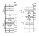
- FIG. 1 shows relevant layers of a multi-state current-switching magnetic memory element 100 are shown, in accordance with an embodiment of the present invention.
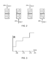
- FIG. 2 shows various states of the memory element 100 .
- FIG. 3 shows a graph of the level of resistance (R) of each of the layers 118 , 114 , 110 and 106 (shown in the y-axis) vs. the state of the memory element 100 .
- FIG. 4 shows a graph 250 of the tunneling magneto resistance (TMR), shown in the y-axis, vs. the resistance area (RA).
- TMR tunneling magneto resistance
- FIG. 5 shows.
- FIG. 5 shows relevant layers of a multi-state current-switching magnetic memory element 600 are shown, in accordance with another embodiment of the present invention.
- FIG. 6 shows relevant layers of a multi-state current-switching magnetic memory element 700 , in accordance with yet another embodiment of the present invention.
- FIG. 7 shows relevant layers of a multi-state current-switching magnetic memory element 800 , in accordance with still another embodiment of the present invention.
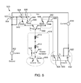
- FIG. 8 shows a program/erase circuit for programming and/or erasing the memory elements of the various embodiments of the present invention.
- FIG. 9 shows a read circuit for reading the memory elements of the various embodiments of the present invention.
- FIG. 10 shows relevant layers of multi-state STTMRAM 1100 , in accordance with an embodiment of the present invention.
- FIG. 11 shows relevant layers of multi-state STTMRAM 1153 , in accordance with an embodiment of the present invention.
- FIG. 12 shows relevant layers of multi-state STTMRAM 1155 , in accordance with an embodiment of the present invention.
- FIG. 13 shows relevant layers of multi-state STTMRAM 1160 , in accordance with an embodiment of the present invention.
- FIG. 14 shows relevant layers of multi-state STTMRAM 1164 , in accordance with an embodiment of the present invention.
- FIG. 15 shows relevant layers of multi-state STTMRAM 1166 , in accordance with an embodiment of the present invention.
- FIG. 16 shows relevant layers of multi-state STTMRAM 1170 , in accordance with an embodiment of the present invention.
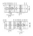
- FIG. 17 shows relevant layers of multi-state STTMRAM 1180 , in accordance with an embodiment of the present invention.
- FIG. 18 shows relevant layers of multi-state STTMRAM 1192 , in accordance with an embodiment of the present invention.
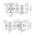
- FIG. 19 shows relevant layers of multi-state STTMRAM 1200 , in accordance with an embodiment of the present invention.
- FIG. 20 shows relevant layers of multi-state STTMRAM 1300 , in accordance with an embodiment of the present invention.
- FIG. 21 shows relevant layers of multi-state STTMRAM 1400 , in accordance with an embodiment of the present invention.
- FIG. 22 shows relevant layers of multi-state STTMRAM 1500 , in accordance with an embodiment of the present invention.
- FIG. 23 shows relevant layers of multi-state STTMRAM 1600 , in accordance with an embodiment of the present invention.
- FIG. 24 shows relevant layers of multi-state STTMRAM 1700 , in accordance with an embodiment of the present invention.
- FIG. 25 shows relevant layers of multi-state STTMRAM 1800 , in accordance with an embodiment of the present invention.
- FIG. 26 shows a flow chart of the steps performed, during a write or program operation, to write/program the multi-state STTMRAM, in accordance with an embodiment of the present invention.
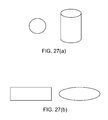
- FIG. 27( a ) shows top-down or in-plane view and side-view of shapes that any of the STTMRAMs 1100 , 1153 , 1155 , 1160 , 1164 , 1166 or 1700 can have when their free and fixed layers have perpendicular magnetic orientation.
- FIG. 27( b ) shows top-down or in-plane view and side-view of shapes that any of the STTMRAMs 1100 , 1153 , 1155 , 1160 , 1164 , 1166 or 1700 can have when their free and fixed layers have in-plane magnetic orientation.
- Table 1 shows certain exemplary characteristics of the embodiments of FIGS. 1 , 5 and 6 .
- Table 2 shows certain exemplary characteristics of the embodiment of FIG. 7 .
- a multi-state magnetic memory cell is disclosed.
- a stack of magnetic tunnel junction (MTJ) is formed, each MTJ being formed of at least three layers, a barrier layer formed between a fixed layer and a free layer, each MTJ being separated from another by a conductive layer, the stack forming a multi-state magnetic memory cell for storing at least two bits of digital information.
- MTJ magnetic tunnel junction
- the memory element 100 is shown to include a bottom electrode 122 on top of which is shown formed a pinning layer 120 on top of which is shown formed a fixed layer 118 , on top of which is shown formed a barrier layer 116 , on top of which is formed a free layer 114 , on top of which is shown formed a non-magnetic layer 112 , on top of which is shown formed a free layer 110 , on top of which is shown formed a barrier layer 108 , on top of which is shown formed a fixed layer 106 , on top of which is shown formed a pinning layer 104 , on top of which is shown formed a top electrode 102 .
- the top electrode 102 and the bottom electrode 122 are each made of Tantalum (Ta) in an exemplary embodiment although other suitable materials are contemplated.
- the layers 114 , 116 and 118 are shown to form a MTJ 126 separated by the layer 112 from an MTJ 124 , which is formed from the layers 106 , 108 and 110 .
- the MTJ 124 and 126 form the relevant parts of a stack of memory elements. In fact, while two MTJs are shown to form the stack of FIG. 1 , other number of MTJs may be stacked for storing additional bits of information.
- the MTJ 126 is for storing a bit of information or two states, ‘1’ and ‘0’, while the MTJ 124 is for storing another bit of information and since each bit represents two binary states, i.e. ‘1’ and ‘0’, two bits represent four binary states, generally represented as ‘00’, ‘01’, ‘10’, ‘11’, or 0, 1, 2 and 3 in decimal notation, respectively.
- the memory element 100 advantageously stores two bits of information thereby decreasing the real estate dedicated for memory and further increases system performance. This is particularly attractive for embedded memory applications. Additionally, manufacturing is made easier and less costly and scalability is realized.
- each of the MTJs acts as a filter for electrons with different spins giving rise to different amounts of tunneling current for electrons with different spins thereby causing two unique resistance values associated with each MTJ for two different orientations of the free layer.
- each MTJ similarly has associated therewith, a unique resistance value.
- the layers 104 and 120 are each typically formed substantially of IrMn or PtMn or NiMn or any other material including Manganese (Mn).
- the layers 106 and 118 are typically formed substantially of a magnetic material. Examples of such magnetic material include CoFeB or CoFe/Ru/CoFeB.
- the layers 108 and 116 are each made substantially of a non-magnetic material, an example of which is magnesium oxide (MgO).
- the layer 112 is a non-magnetic layer made substantially of, for example, NiNb, NiP, NiV or CuZr.
- the layer 112 serves to insulate the two MTJs 124 and 126 from one another. In an embodiment employing more than two MTJs, another layer, such as the layer 112 would be formed on top of the layer 104 or on the bottom of the layer 120 .
- the layers 110 and 114 are each made of CoFeB containing oxides intermixed. The layers 110 and 114 are substantially amorphous in an at-deposited state.
- the top electrode 102 and the bottom electrode 122 are each made of tantalum (Ta), in one embodiment of the present invention, however, other types of conductive material may be employed.
- the layers 120 and 104 are anti-ferromagnetic (AF) coupling layers. More specifically, for example, the magnetic moment of the layer 104 helps to pin the magnetic moment of the layer 106 . Similarly, the magnetic moment of the layer 120 serves to pin the magnetic moment of the layer 118 . The magnetic moment of each of the layers 120 and 104 are permanently fixed.
- AF anti-ferromagnetic
- the layers 108 and 116 are aluminum oxide (Al2O3) and titanium oxide (TiO2).
- a thin-layer of one of the constituent elements may be deposited prior to the deposition of the barrier oxide layer.
- a 2-5 A thick Mg layer may be deposited prior to the deposition of the layers 108 and 116 . This limits any damage of the magnetic-free layer from intermixing of the elements during deposition.
- the layer 112 is a non-magnetic layer which is substantially amorphous made of, for example, Nickel niobium (NiNb), Nickel phosphorous (NiP), Nickel vanadium (NiV), Nickel bororn (NiB) or copper-zirconium (CuZr).
- the layer 112 serves to isolate the two MTJs 124 and 126 from one another. In an embodiment of the present invention, which employs more than two MTJs, another layer, such as the layer 112 would be formed on top of the layer 104 or on the bottom of the layer 120 .
- the layers 110 and 114 are each made of CoFeB containing oxides intermixed. The layers 110 and 114 are substantially amorphous in an as-deposited state.
- the top and the bottom electrodes are typically made of tantalum (Ta).
- the layers 120 and 104 are anti-ferromagnetic (AF) coupling layers. More specifically, for example, the magnetic moment of the layer 104 helps to pin the magnetic moment of the layer 106 . Similarly, the magnetic moment of the layer 120 serves to pin the magnetic moment of the layer 118 .
- the magnetic moment of each of the layers 120 and 104 are permanently fixed. This is typically done by a magnetic annealing process following the deposition of all the layers and involves heating the wafer consisting of at least one memory element 100 under the application of a substantially uni-axial magnetic field of over 5 kilo-Oersteds and a temperature of over 350 degree centigrade for typically 2 hours. This annealing process also serves to re-crystallize the layers 108 and 116 and their respective adjacent free layers 110 and 114 . This process is essential for making high performing magnetic tunnel junctions.
- AF anti-ferromagnetic
- Typical thicknesses for each of the layers of the memory element 100 are now presented. However, these sizes are merely examples, as other thicknesses are anticipated.
- a typical thickness of each of the top electrode 102 and the bottom electrode 122 is 30 to 200 nm. While a preferred thickness is typically 50 nm, the actual thickness choice may depend on the requirements from the metallization process.
- the layers 104 and 120 are typically 20 to 100 nm in thickness with a preferred thickness of 25-50 nm.
- the layers 108 and 118 are typically made of three layers of Cobalt-Iron (CoFe)/Ruthenium (Ru)/Cobalt-Iron-Boron (CoFeB) with CoFe layer being placed adjacent to the layers 104 and 120 .
- the typical thickness of the CoFe layer is 3 to 10 nm
- Ru layer is 0.6 to 1.0 nm to create anti-ferromagnetic coupling between the two adjacent magnetic layers of CoFe and CoFeB.
- the CoFeB layer is typically 2 to 10 nm thick with a preferred range of 2.5 to 5 nm.
- the free layers 110 and 114 are typically 2 to 7 nm thick with a preferred range of 2-5 nm and may contain a 1-2 nm thick layer of Co—Fe-oxide inter-dispersed in that layer in order to get low switching current during current induced switching.
- the barrier layers 108 and 116 are typically 0.8 to 3 nm.
- the two barrier layers may have slightly different thickness, for example layer 116 can be 1.5 to 2.5 nm thick while the second barrier layer 108 may be 0.8 to 1.2 nm thick, and vice-versa. Additionally, the thickness and the amounts of oxide in the free-layers 110 and 114 may be different by a factor of 1.5 or higher.
- the non-magnetic layer 112 is typically 2 to 50 nm thick with a preferred range being 2 to 10 nm. It should be pointed out that while the [most] preferred material choice of the non-magnetic isolation layer 112 consists of amorphous non-magnetic alloys, a crystalline non-magnetic alloy may also work.
- the layers of the memory element 100 are formed in the manner described hereinabove. Additionally, an annealing process, which is well known, is performed heating the memory element 100 in the presence of a magnetic field after which channels are formed in each of the layers 108 and 116 . Following the annealing process, the fixed layers 106 and 118 are oriented in a particular orientation, and the layers 108 and 116 well as the layers 110 and 114 , take on crystalline characteristics.
- the MTJs 124 and 126 are made with different aspect ratios (or anisotropy), the switching current is different for these two MTJs.
- the aspect ratio for MTJ 124 is approximately 1:1.3 to 1:1.5 while the aspect ratio for the MTJ 126 is approximately 1:2 to 1:2.5.
- the switching current for the MTJ 126 is 3-5 times higher than that of the MTJ 124 , in the foregoing embodiment. At high current levels both MTJs switch magnetic orientation, while at low current levels only the MTJ 124 having the smaller aspect ratio switches.
- the state of the magnetic moment of each of the layers of the MTJ defines the state of the memory element 100 .
- the layers 104 and 120 each act as AF coupling layers, they pin or switch the magnetic moments of the their neighboring fixed layer, which, then, by the application of current, causes neighboring free layers to switch or not.
- the layer 118 defines one state
- the layer 114 defines another state
- the layer 110 defines yet another state
- the layer 106 defines still another state.
- the states of each of the layers 118 , 114 , 110 and 106 are referred to as states 1 , 2 , 3 and 4 , respectively.
- FIG. 2 shows various states of the memory element 100 . Due to the use of two MTJs, four different states or two bits may be stored, therefore, the states 1 - 4 are shown.
- the directions of the arrows indicate the direction of the magnetic moments of free layers and pinning layers.
- the direction of the arrow 200 shows the direction of high current applied to the memory element 100 and in this case, the state of the memory element 100 is at an all ‘1’s or all ‘0’s state.
- the direction of the arrow 202 shows the direction of low current applied to the memory element 100 when at state 1 .
- the direction of the arrow 204 shows the direction of high current applied to the memory element 100 when the latter is at state 2 and the direction of the arrow 206 shows the direction of low current applied to the memory element 100 when at state 3 .
- FIG. 3 shows a graph of the level of resistance (R) of each of the layers 118 , 114 , 110 and 106 (shown in the y-axis) vs. the state of the memory element 100 .
- the memory element 100 has taken on the state 1 (corresponding to 202 on FIG. 2 )
- the memory element 100 has taken on the state 2 (corresponding to 204 on FIG. 2 )
- the memory element 100 has taken on the state 3 (corresponding to 206 on FIG. 2 )
- the memory element 100 has taken on the state 4 (corresponding to 200 on FIG. 2 ).
- the level of resistance for each of these states is indicated in Table 1, at a column labeled “Total R”.
- Total R the level of resistance for each of these states is indicated in Table 1, at a column labeled “Total R”.
- the R, in FIG. 3 is indicated as being 3 kilo ohms (K Ohms) by Table 1.
- the R, in FIG. 3 is indicated as being 4 K Ohms and so on.
- the values used for resistance serve as examples only such that other values may be employed without departing from the scope and spirit of the present invention.
- different aspect ratio or anisotropy associated with the different MTJs 124 and 126 causes the different switching of the MTJs, which results in two bits being stored in the memory element 100 .
- the size of the barrier layers of the MTJs are changed to effectuate different resistances.
- the size of the MTJs are changed to the same.
- FIG. 4 shows a graph 250 of the tunneling magneto resistance (TMR), shown in the y-axis, vs. the resistance area (RA).
- TMR tunneling magneto resistance
- RA resistance area
- Rh is resistance at a high state and Rl is resistance at a low state.
- the graph 250 of FIG. 4 serves merely as an example to convey the difference in TMR or percentage increase as the RA increases. For instance, at an RA of 2 ohm-micro-meters squared, the TMR is 100% while at a RA of 10, the TMR is 150% where the thickness of the barrier layer of the MTJ is between 14-24 Angstroms.
- FIG. 5 shows relevant layers of a multi-state current-switching magnetic memory element 600 are shown, in accordance with another embodiment of the present invention.
- the memory element 600 is shown to include a bottom electrode 122 on top of which is shown formed a pinning layer 120 on top of which is shown formed a fixed layer 118 , on top of which is shown formed a barrier layer 116 , on top of which is formed a free layer 114 , on top of which is shown formed a non-magnetic layer 112 , as that shown in FIG. 1 .
- the MTJ 126 comprises the layers 114 , 116 and 118 .
- FIG. 1 shows relevant layers of a multi-state current-switching magnetic memory element 600 are shown, in accordance with another embodiment of the present invention.
- the memory element 600 is shown to include a bottom electrode 122 on top of which is shown formed a pinning layer 120 on top of which is shown formed a fixed layer 118 , on top of which is shown formed a barrier layer 116
- the MTJ 612 which is made of a free layer 602 , a barrier layer 604 and a fixed layer 606 , is smaller, in its planar dimension, than the MTJ 126 of FIG. 1 , which causes the MTJ 612 to have a different resistance than that of the MTJ 126 .
- the free layer 602 is shown to be formed on top of the layer 112 and on top of the layer 602 is shown formed the layer 604 , on top of which is shown formed the layer 606 , on top of which is shown formed a pining layer 608 , a top electrode 610 .
- the MTJs 126 and 612 are shown separated by the layer 112 .
- the MTJs 126 and 612 form the relevant parts of a stack of memory elements. In fact, while two MTJs are shown to form the stack of FIG. 5 , other number of MTJs may be stacked for storing additional bits of information.
- the difference in the planar dimension of the MTJs 612 to that of the MTJ 126 is approximately 1 to 10 and typically 1 to 3, in one embodiment of the present invention.
- the material for each of the layers of the memory element 600 may be the same as that of counterpart layers of the memory element 100 .
- the layer 602 is made of the same material as that of the layer 110 and the layer 604 is made of the same material as that of the layer 108 and the layer 606 is made of the same material as the layer 106 and the layer 608 is made of the same material as the layer 104 .
- the top electrodes 610 and 102 are made of the same material.
- the MTJ 612 may be larger, in size, in the same planar dimension, than the MTJ 126 .
- FIG. 6 shows relevant layers of a multi-state current-switching magnetic memory element 700 , in accordance with yet another embodiment of the present invention.
- the memory element 700 to include a bottom electrode 122 on top of which is shown formed a pinning layer 120 on top of which is shown formed a fixed layer 118 , on top of which is shown formed a barrier layer 116 , on top of which is formed a free layer 114 , on top of which is shown formed a non-magnetic layer 112 , as that shown in FIGS. 1 and 6 .
- the MTJ 126 comprises the layers 114 , 116 and 118 .
- FIG. 1 and 6 the embodiment of FIG.
- the MTJ 714 which is shown to comprise a free layer 710 , a barrier layer 708 and a fixed layer 706 , is shown to be smaller in its planar dimension than the MTJ 126 causing the MTJ 714 to have a different resistance than that of the MTJ 126 .
- the MTJs 126 and 714 are shown separated by the layers 702 and 704 .
- the layer 704 serves to pin the layer 706 while the layer 702 serves to isolate the MTJ 126 and is an amorphous only to the layer 114 .
- the layer 702 in one embodiment of the present invention, is made of two non-magnetic layers, such as Ta and/or an amorphous alloy, the same as Nickel-niobium (NiNb) or nickel-phosphorus (NiP).
- the MTJs 126 and 612 form the relevant parts of a stack of memory elements. In fact, while two MTJs are shown to form the stack of FIG. 5 , other number of MTJs may be stacked for storing additional bits of information.
- the difference in the planar dimension of the MTJs 714 to that of the MTJ 126 is 1 to 10, and typically 1 to 3 in one embodiment of the present invention.
- the material for each of the layers of the memory element 700 may be the same as the counterpart layers of the memory element 100 or that of the memory element 600 .
- the layer 710 is made of the same material as that of the layer 110 and the layer 708 is made of the same material as that of the layer 108 and the layer 706 is made of the same material as the layer 106 and the layer 704 is made of the same material as the layer 104 .
- the top electrodes 712 and 102 are made of the same material.
- the MTJ 714 may be larger in size in the same planar dimension, than the MTJ 126 .
- FIG. 7 shows relevant layers of a multi-state current-switching magnetic memory element 800 , in accordance with still another embodiment of the present invention.
- the memory element 800 is shown to include a bottom electrode 802 on top of which is shown formed a pinning layer 804 on top of which is shown formed two fixed layers on either side thereof. That is, a fixed layer 806 is shown formed on one side of the layer 804 and a fixed layer 808 is shown formed on an opposite side of the layer 804 .
- two MTJs are shown formed on either side or top of the layer 804 .
- an MTJ 820 is shown formed on one side of the layer 804 and another MTJ 822 is shown formed on an opposite side of the layer 804 .
- the MTJ 820 includes the fixed layer 806 , which is formed on top of the layer 804 and the barrier layer 810 shown formed on top of the layer 806 and the free layer 812 shown formed on top of the layer 810 .
- the MTJ 822 is shown to include the fixed layer 808 , which is formed on top of the layer 804 and the barrier layer 814 , which is shown formed on top of the layer 808 and the free layer 816 , which is shown formed on top of the layer 814 .
- a top electrode 818 is shown formed on top of the MTJs 820 and 822 , or more specifically on top of the layers 812 and 816 .
- the top electrode 818 is typically made of two layers, such as Ta and a conductive, non-magnetic material.
- the layer 804 is formed on top of the bottom electrode and the layers of the MTJs 820 and 822 are formed on top of the layer 804 and on top of the MTJs 820 and 822 is formed the top electrode 818 .
- the layers of the MTJs 820 and 822 are formed uniformly and continuously on top of the layer 804 and a trench 824 , which is basically an empty space or hole is formed, prior to depositing the top electrode 818 , by etching through the layers of the MTJs 820 and 822 .
- the fixed layers of the MTJs 820 and 822 are the same layer prior to etching and the barrier layers of the MTJs 820 and 822 are the same layer prior to etching and the free layers of the MTJs 820 and 822 are the same layer prior to etching.
- the trench 824 is filled with a dielectric material, such as silicon dioxide (SiO2) or silicon nitride (SiNx) to enhance stability.
- a dielectric material such as silicon dioxide (SiO2) or silicon nitride (SiNx) to enhance stability.
- the top electrode 818 is deposited or formed on top of the MTJs 820 and 822 .
- the embodiment of FIG. 7 as the embodiments of FIGS. 6 , 5 , and 1 store two bits of information, with one bit stored in each MTJ.
- the MTJ 820 is for storing one bit
- the MTJ 822 is for storing another bit of information.
- more bits may be stored by adding MTJs.
- additional MTJs may be added on top of the layer 804 or the MTJs 820 and 822 .
- additional trenches are formed between the MTJs, such as the trench 824 .
- Table 2 shows certain exemplary characteristics of the embodiment of FIG. 7 . It should be noted that similarly, Table 1 shows certain exemplary characteristics of the embodiments of FIGS. 1 , 5 and 6 .
- each state represents a binary value such that four states, and represented by two bits are stored.
- the programming current, in micro amps, i.e. the current needed to program the memory element 800 to a given state, is indicated in the last column of Table 2, under the label “Prog I”.
- a non-uniform switching based non-volatile magnetic memory element such as the non-uniform switching based non-volatile magnetic memory element 100 disclosed in U.S. patent application Ser. No. 11/674,124 entitled “Non-Uniform Switching Based Non-Volatile Magnetic Base Memory”, filed on Feb. 12, 2007, may be employed to replace the MTJs of the various embodiments shown and discussed herein.
- the MTJ 124 or the MTJ 126 may be replaced with a non-uniform switching based non-volatile magnetic memory element.
- Other MTJs discussed herein may also be replaced with non-uniform switching based non-volatile magnetic memory element. This advantageously further reduces the requisite switching current to enhance system performance.
- FIG. 8 shows a program/erase circuit for programming and/or erasing the memory elements of the various embodiments of the present invention.
- a current source 902 is shown coupled to a current mirror circuit 904 , which is shown coupled to the switch 906 , which is, in turn, shown coupled to the switch 968 , which is shown coupled to the multi-state current-switching magnetic memory cell 914 , which is shown coupled to the switch 916 .
- a current source 918 is shown coupled to a current mirror circuit 920 and further shown coupled to Vcc on an opposite end thereto.
- the circuit 920 is further shown coupled to the switch 999 .
- the circuit 904 is shown to include a P-type transistor 922 , a P-type transistor 924 and a P-type transistor 926 .
- the source of each of the transistors 922 , 924 and 926 are shown coupled to Vcc.
- Vcc is at a predetermined voltage level that is higher than ground.
- the gate of the transistor 922 is shown coupled to the current source 902 and the opposite side of the current source 902 is shown coupled to ground.
- the drain of the transistor 922 is shown coupled to its gate as well as to the gate of the transistor 924 and the gate of the transistor 926 .
- the drains of the transistors 924 and 926 are shown coupled to the switch 906 .
- the memory cell 914 is shown to include an MTJ 910 , an MTJ 912 and an access transistor 940 .
- the MTJ 912 is shown coupled in series to the MTJ 912 , which is shown coupled to the drain of the transistor 940 .
- the gate of the transistor 940 is shown coupled to the word line 942 .
- the word line 942 selects a memory cell.
- the source of the transistor 940 is shown coupled to the switch 916 .
- memory cell 914 is shown to include two MTJs coupled in series, it is contemplated that the memory cell 914 can include more than two MTJs and that which would be coupled together in series. In this case, each MTJ may have a different switching current associated therewith.
- the circuit 920 is shown to include an N-type transistor 928 , an N-type transistor 930 and an N-type transistor 932 .
- the drains of the transistors 928 , 930 and 932 are shown coupled to ground.
- the gate of the transistor 932 is coupled to the current source 918 and is further coupled to the drain of the transistor 932 and is further coupled to the gate of the transistor 930 as well as to the gate of the transistor 928 .
- the drain of the transistors 930 and 928 are shown coupled to the switch 999 .
- Each of the switches 968 and 916 are shown operative to switch between two states, a program state and an erase state.
- the switches 906 and 999 are shown operative to switch between two states.
- the MTJs 910 and 912 are similar to the MTJs of previous figures, such as those depicted in FIGS. 1 and 6 .
- the MTJs 910 and 912 coupled in parallel, would be similar to the MTJs shown in FIG. 7 .
- Each MTJ 910 and 912 possesses a resistance of a different or unique value. The difference in their resistance results from the difference in the aspect ratio or size or anisotropy of the MTJs.
- the size of the transistor 926 is greater than the size of the transistors 922 and 924 .
- the size of the transistor 928 is greater than the size of the transistors 930 and 932 .
- the size difference of the foregoing transistors is 4 to 1.
- a current of level of 50 micro Amps is applied by the current source 902 to the circuit 904 , which is amplified to 4 ⁇ the current level or 200 micro Amps, as shown in Table 1 because the transistor 926 is able to drive this level of current.
- the switch 908 is set to ‘program’ state, as is the switch 916 , which causes the 200 micro amp current to flow through the MTJs 910 and 912 and the transistor 940 is selected by raising the voltage on the word line 942 .
- This results in programming of state 1 The magnetic moment of the free layers of the MTJs 910 and 912 will be caused to be aligned with the magnetic moment of that of their respective fixed layers. This results in the lowest resistance of the memory cell 914 , as indicated in Table 1.
- a current of level of 50 micro Amps is applied by the current source 918 to the circuit 920 , which is the same current level as that generated by the circuit 920 .
- the current level for state 2 is indicated in Table 1.
- the switch 999 is caused to be switched to the state indicated at 948 .
- the switches 908 and 916 are both set to ‘erase’ state, which causes the 50 micro amp current to flow through the MTJs 910 and 912 and the transistor 940 is selected by raising the voltage on the word line 942 . This results in programming of state 2 .
- the magnetic moment of the free layer of the MTJ 910 is caused to be switched to an anti-parallel state or a state that is in opposite to being aligned with its respective fixed layer.
- the MTJ 912 remains in the state it was in at state 1 .
- the reason for this is, that in one embodiment of the present invention, with the aspect ratio of the MTJ 912 being higher than that of MTJ 910 , it is prevented from switching. This results in the resistance of the memory cell 914 indicated in Table 1.
- a current of level of 50 micro Amps is applied by the current source 918 to the circuit 920 , which causes the current level, generated by the transistor 928 to be 4 times that of the level of the current source, or 200 micro amps.
- the current level for state 3 is indicated in Table 1.
- the switch 910 is caused to be switched to the state indicated at 950 .
- the switches 908 and 916 are both set to ‘erase’ state, which causes the 200 micro amp current to flow through the MTJs 910 and 912 and the transistor 940 is selected by raising the voltage on the word line 942 . This results in programming of state 3 .
- the magnetic moment of the free layers of the MTJs 910 and 912 are caused to be switched to an anti-parallel state relative to their respective fixed layers. This results in the resistance of the memory cell 914 to be that indicated in Table 1.
- a current of level of 50 micro Amps is applied by the current source 902 to the circuit 904 , which is the current level of the circuit 904 and that which is indicated in Table 1 for state 4 .
- the switch 908 is set to ‘program’ state, as is the switch 916 , which causes the 50 micro amp current to flow through the MTJs 910 and 912 and the transistor 940 is selected by raising the voltage on the word line 942 .
- This results in programming of state 4 The magnetic moment of the free layer of the MTJ 910 will be caused to be aligned with the magnetic moment of that of its respective fixed layer.
- the MTJ 912 remains in its anti-parallel state, the reason for this is due the difference in the aspect ratios of the two MTJs as discussed hereinabove. This results in a resistance of the memory cell 914 indicated in Table 1.
- FIG. 9 shows a read circuit for reading the memory elements of the various embodiments of the present invention.
- FIG. 9 is shown to include a memory cell 1002 coupled to a sense amplifier circuit 1004 , which is shown coupled to a reference circuit 1006 .
- the memory cell 1002 is shown to include an access transistor 1008 , an MTJ 1010 and an MTJ 1012 .
- the transistor 1008 is shown to have a drain, a source and a gate.
- the gate of the transistor 1008 is shown coupled to a word line 1014 , the drain of the transistor is shown coupled to ground and the source of the transistor is shown coupled to the MTJ 1010 .
- the circuit 1006 is shown to include a number of state reference circuits, indicated as state reference circuit 1020 , 1022 and 1024 .
- Each of the circuits 1020 - 1024 includes an access transistor and a reference resistor.
- the circuit 1020 is shown to include a reference resistor 1026 coupled on one side to the circuit 1004 and Vcc and on the other side to the drain of an access transistor 1028 .
- the gate of the transistor 1028 is shown coupled to a select signal, namely select 1 signal 1040 .
- the circuit 1022 is shown to include a reference resistor 1030 coupled on one side to the circuit 1004 and Vcc and on the other side to the drain of an access transistor 1032 .
- the gate of the transistor 1032 is shown coupled to a select signal, namely the select 2 signal 1042 .
- the circuit 1024 is shown to include a reference resistor 1034 coupled on one side to the circuit 1004 and Vcc and on the other side to the drain of an access transistor 1036 .
- the gate of the transistor 1044 is shown coupled to a select signal, namely the select 3 signal 1044 .
- the MTJs 1010 and 1012 are similar to the MTJs of the embodiments of the present invention except that in the case of FIG. 7 , the MTJs of the read circuit would be coupled in parallel rather than in series, shown in FIG. 9 .
- the memory cell 1002 is selected by raising the voltage of the word line 1014 .
- the circuit 1004 compares the total resistance of the MTJs 1010 and 1012 with the resistances of the reference resistors of the state reference circuits. For example, the resistance of the MTJs 1010 and 1012 (collectively or added together) is compared to the resistance of the resistor 1026 and if it is determined to be less, the state of the memory cell 1002 is declared as binary value ‘00’ or perhaps, state 1 .
- the former is then compared to the resistance of the resistor 1030 and there again, if the resistance of the MTJs 1010 and 1012 is less than the resistor 1030 , the state 2 or binary value ‘01’. If the resistance of the MTJs 1010 and 1012 is determined to be greater than the resistor 1030 , the resistance of the MTJs 1010 and 1012 is compared to the resistance of the resistor 1034 and if the resistance of the former is determined to be lower, the state 3 or binary value ‘10’ is declared (or read), otherwise, the state 4 or binary value ‘11’ is declared.
- the select signal of each of the circuits 1020 - 1024 are used to select the corresponding circuit. For example, to compare the resistance of the MTJs to the resistance of the resistor 1026 , the signal 1040 is activated thereby turning on the transistor 1028 . In the meanwhile, the remaining transistors of the circuit 1006 are off. Similarly, to compare the resistance of the MTJs to the resistance of the resistor 1030 , the signal 1042 is activated thereby turning on the transistor 1032 . In the meanwhile, the remaining transistors of the circuit 1006 are off. To compare the resistance of the MTJs to the resistance of the resistor 1034 , the signal 1044 is activated thereby turning on the transistor 1036 . In the meanwhile, the remaining transistors of the circuit 1006 are off.
- Examples of resistance values of the reference resistors are averages of the resistances of the MTJs 1010 and 1012 .
- the resistance of the resistor 1026 is the average of the resistances of the MTJs 1010 and 1012 at the states 1 and 4 , as indicated in Table 1.
- the resistance of the resistor 1030 is the average of the resistances of the MTJs 1010 and 1012 at the states 2 and 4 , as indicated in Table 1.
- the resistance of the resistor 1034 is the average of the resistances of the MTJs 1010 and 1012 at the states 2 and 3 , as indicated in Table 1.
- the resistor 1026 has a resistance of 3.5 kilo-ohm, which is the average of 3 and 4 kilo-ohms.
- the resistance of the resistor 1030 is 4.5 kilo-ohms, which is the average of 5 and 4 kilo-ohms and the resistance of the resistor 1034 is 5.5 kilo-ohms, which is the average of 5 and 6 kilo-ohms.
- a STTMRAM using two or more MTJs having perpendicular orientations or a combination of perpendicular and longitudinal MTJs, placed in the close proximity to each other is disclosed.
- One of the characteristics of such a STTMRAM is to advantageously have multiple resistances associated therewith allowing for the storage of multiple states, thereby having smaller cell size.
- the magnetic memory bits At smaller litho dimensions the magnetic memory bits would have substantially perpendicular orientation of the magnetization direction.
- Bottom MTJ is a memory structure where the fixed layer is formed below the free layer during MTJ fabrication and a top MTJ (or stack) is memory structure where the fixed layer is formed on top of the free layer during MTJ fabrication.
- FIG. 10 shows a multi-state spin-torque transfer magnetic random access memory (STTMRAM) 1100 , in accordance with an embodiment of the present invention.
- the multi-state STTMRAM memory 1100 is shown to include bottom electrode (BE) 1104 , underlayer 1106 , fixed layer 1108 , spin polarization enhanced (interface) layers (SPEL) 1110 and 1114 , free layer 1118 , cap layer 1120 , non-magnetic spacing layer 1122 , underlayer 1128 , fixed layer 1130 , SPEL 1134 , tunneling layer 1136 , SPEL 1138 , free layer 1140 , cap layer 1141 and top electrode (TE) 1143 .
- BE bottom electrode
- SPEL spin polarization enhanced
- SPEL spin polarization enhanced (interface) layers
- Underlayer 1106 is shown formed on top of BE 1104 , which is generally formed on a substrate or film (or a metal post or line such as tungsten, aluminum or copper for) of a typical integrated circuit.
- Fixed layer 1108 is shown formed on top of fixed layer 1108 and SPEL layer 1110 is shown formed on top of fixed layer 1108 .
- SPEL 1110 is a part of fixed layer 1108 . In some embodiments, SPEL 1114 is a part of free layer 1118 .
- tunneling layer 1112 is shown formed on top of SPEL 1110
- SPEL 1114 is shown formed on top of tunneling layer 1112
- free layer 1118 is shown formed on top of SPEL 1114
- cap layer 1120 is shown formed on top of free layer 1118
- non-magnetic spacing layer 1122 is shown formed on top of cap layer 1120
- underlayer 1128 is shown formed on top of non-magnetic spacing layer 1122
- fixed layer 1130 is shown formed on top of underlayer 1128
- SPEL 1134 is shown formed on top of fixed layer 1130
- tunneling layer 1136 is shown formed on top of SPEL 1134
- SPEL 1138 is shown formed on top of tunneling layer 1136
- free layer 1140 is shown formed on top of SPEL 1138
- cap layer 1141 is shown formed on top of free layer 1140
- TE 1143 is shown formed on top of cap layer 1141 .
- Magnetic tunnel junction (MTJ) 1124 comprises fixed layer 1108 , SPEL 1110 , tunneling layer 1112 , SPEL 1114 and free layer 1118 .
- MTJ 1126 comprises fixed layer 1130 , SPEL 1134 , tunneling layer 1136 , SPEL 1138 and free layer 1140 . In this manner, MTJ 1126 and MTJ 1124 are stacked. While MTJ 1124 and MTJ 1126 are each shown to have a bottom stacking structure with their respective free layers formed above their fixed layers, alternatively, they may have a top stacking structure where their respective fixed layers are formed above their free layers.
- SEPL 1134 , tunneling layer 1136 and SPEL 1138 are collectively referred to as sub-magnetic tunnel junction (sub-MTJ) layer 1132 .
- SEPL 1110 , tunneling layer 1112 and SPEL 1114 are collectively referred to as sub-magnetic tunnel junction (sub-MTJ) layer 1159 .
- ULs 1106 and 1128 may be multi-layered with one or more layers of underlayer or at least one layer of seed layer. Seed layers are well known to those skilled in the art.
- SPELs are not employed in either of MTJs 1124 or 1126 , in other embodiments, one of the MTJs 1124 or 1126 employs SPELs and another does not. In yet another embodiment, only one SPEL is used adjacent to the tunneling layer. That is, for example, only SPEL 1110 is used and SPEL 1114 is absent or only SPEL 1114 is used and SPEL 1110 is absent. In yet other embodiments, as discussed above, SPEL is part of an adjacent layer. For example, SPEL 1134 is part of fixed layer 1130 or SPEL 1138 is part of free layer 114 or SPEL 1134 is part of fixed layer 1130 and SPEL 1138 is part of free layer 1140 .
- BE 1104 and TE 1143 are as known to those skilled in the art.
- Fixed layers 1108 and 1130 each have a magnetization direction (or orientation) that is fixed at the time of manufacturing and throughout the operational lifetime of the multi-state STTMRAM cell 1100 .
- the magnetization direction of each of the free layers 1118 and 1140 switches between a parallel state and an anti-parallel state relative to the magnetization direction of each of their respective fixed layers during operation of the multi-state STTMRAM 1100 .
- the parallel and anti-parallel states define the logical state of a free layer which define the logical state of the corresponding MTJ.
- free layer 1118 's magnetization state being in a parallel state relative to fixed layer 1108 defines a different logical state than free layer 1118 's magnetization direction being in an anti-parallel state relative to fixed layer 1108 .
- An example of logic states are ‘0’ or ‘1’.
- the direction of magnetization of fixed layer 1108 which is shown by the arrow 1123 , is fixed in the direction of the arrow 1123 and it is perpendicular to the surface of the substrate onto which the multi-state STTMRAM 1100 is formed.
- the direction of magnetization of free layer 1118 which switches relative to that of fixed layer 1108 , as shown by the arrow 1127 , is also perpendicular to the plane of the substrate.
- the thickness of each of underlayers 1106 and 1128 is typically between 5 nano meters (nm) to 50 nm and may comprise a seedlayer underneath or in between BE 1104 and underlayer 1106 and in between non-magnetic spacing layer 1122 and underlayer 1128 .
- the seedlayer thickness is 2 nm to 50 nm.
- fixed layers 1108 and 1130 are 2 nm to 100 nm.
- the thickness of SPEL layer is typically less than 5 nm.
- the thickness of each of the free layers 1118 and 140 is typically 1 to 10 nm.
- the thickness of each of tunneling layers 1112 and 1136 is typically 0.5 to 3.0 nm.
- the thickness of non-magnetic isolation layer 1122 is 5 nm-100 nm. In some embodiments, the thickness of caplayer 1141 is 2 to 100 nm and typically 5 to 50 nm. In some embodiments, the thickness of top electrode 1143 and bottom electrode choice and thickness depend on the device design and are typically thicker than 10 nm.
- each of the underlayers 1106 and 1128 is made of are typically chosen from alloys of one or more of the elements chosen from tantalum (Ta), chromium (Cr), titanium (Ti), molybdenum (Mo), tungsten (W), boron (B), copper (Cu), nitrogen (N), nickel (Ni), carbon (C), phosphorus (P), iron (Fe), or cobalt (Co) and should be conducting and non-magnetic.
- Fixed layers 1108 and 1130 are each generally alloys of iron (Fe) nickel (Ni) cobalt (Co), platinum (Pt), copper (Cu), boron (B), tantalum (Ta), titanium (Ti), chromium (Cr) including rare earth alloys like terbium (Tb), samarium (Sm), neodymium (Nd), and gadolinium (Gd).
- the magnetic alloy also contains one or more of silicon oxide (SiO2), titanium oxide (TiO2), tantalum oxide (Ta2O5), and aluminum oxide (Al2O3).
- each of the fixed layers 1108 and 1130 is comprised of multi-layers made of Co and Pt with each of the Co and/or Pt layers of each of the multi-layers typically having a thickness of 0.3 nm-2 nm, and the total number of each of the Co and/or Pt layers being less than 10.
- the choice of material for each of SPEL layers 1110 , 1114 , 1134 and 1138 in some embodiments, is an alloy of Co(20-80 at %)Fe(20-80 at %)B(8-25 at %) such that the as-deposited SPEL layer is >80 volume percent amorphous.
- Cap layers 1120 and 1141 are each a nonmagnetic alloy and conducting of one or more of the elements selected from tantalum (Ta), chromium (Cr), tungsten (W), titanium (Ti), zirconium (Zr), niobium (Nb), copper (Cu), or aluminum (Al).
- the function UL 1106 is to provide the proper crystal structure template in order to grow the adjacent and subsequent magnetic fixed layers 1108 and 1130 having perpendicular orientation in a direction shown by arrow 1123 .
- This is typically characterized by measuring the delta theta 50 of the preferred easy axis. As known to those skilled in the art, this is carried out typically by using an x-ray diffractometer such as one designed by Rigaku Coporation, Tokyo, Japan. A smaller delta-theta 50 indicates, such as typically below 5 degrees, a more oriented film. A typical value of the delta-theta50 is below 10 degrees.
- the function of SPEL layer is to enhance the tunneling magneto-resistance (TMR) of the MTJs through proper crystal structure matching during the magnetic annealing process.
- TMR tunneling magneto-resistance
- fixed layers 1108 and 1130 act as a reference layer for respective magnetic tunnel junction (MTJ).
- fixed layer 1108 acts as a reference layer with fixed magnetic orientation for MTJ 1124 and fixed layer 1140 acts as a reference layer with fixed magnetic orientation for MTJ 1126 .
- each of tunneling layers 1112 and 1136 acts as spin-filter layer for the spin tunneling for the MTJ which is important to get high TMR. More specifically, the tunneling layers selectively filter the spin states of the polarized conduction electrons as they travel through the fixed layer to the free layer and vice versa. A detailed description of this can be found in the published paper, “Theory of Tunneling Magnetoresistance For Epitaxial Systems by W. H. Butler, X. G. Zhang, S. Vutukuri, M. Chchiev and T. C. Schulthess, IEEE Trans Mag., vol. 41, No. 10, October 2005”.
- each of free layers 1118 and 1140 is to switch between magnetic orientations (states) when current is applied to the multi-state STTMRAM thereby storing a state.
- the free layer is critical to its corresponding MTJ in that it causes the MTJ to exhibit high tunneling magneto resistance (TMR) characteristic.
- TMR tunneling magneto resistance
- the design and the material of choice used for making the free layer determines, at least in part, the programming current of the multi-state STTMRAM as well as device reliability, more specifically the thermal stability.
- STTMRAM 1100 is shown to include two MTJs, in other embodiments, it may include more than two MTJs. In fact, any number of MTJs may be employed in any of the STTMRAM of the various embodiments of the present invention. In the case where more than two MTJ are employed, a unique switching current switches the state of each MTJ. For example, a STTMRAM with three MTJs, coupled in series, and coupled to an n-channel MOSFEL (NMOS) type of access transistor may exhibit switching currents of 75 micro Amps for one MTJ, 50 micro Amps for a second MTJ and 25 micro Amps for the third MTJ.
- NMOS n-channel MOSFEL
- an MTJ is a variable resistive element.
- any of the MTJs discussed and/or shown herein may be replaced with a variable resistive element without departing from the scope and spirit of the present invention.
- electric current is applied in a direction that is either from BE 1104 through the subsequent layers that are on top of BE 1104 or in a direction from TE 1143 through the subsequent layers formed below TE 1143 .
- FIG. 11 shows a multi-state STTMRAM 1153 , in accordance with an alternative embodiment of the present invention.
- the multi-state STTMRAM 1153 includes MTJ 1126 , which is shown formed on top of the anti-ferromagnetic (AFM) layer 1128 , which is shown formed top of UL 1150
- AFM anti-ferromagnetic
- the top portion of the multi-state STTMRAM 1153 i.e., the layers on top of the fixed layer 1130 are analogous to common layers of that of multi-state STTMRAM 1100 .
- Anti-ferromagnetic (AFM) layer 1128 is shown formed on top of UL 1150 , which is shown formed on top of non-magnetic spacing layer 1152 which is formed on top of the cap layer 1120 , which is shown formed on top of free layer 1118 , which is shown formed on top of SPEL 1114 .
- the layers formed below SPEL 1114 are analogous to that of like locations of multi-state STTMRAM 1100 .
- AFM layer 1148 is shown formed between UL 1106 and fixed layer 1108 .
- UL 1106 is shown formed on top of BE 1104 , which is typically formed on film or substrate of an integrated circuit.
- the embodiment of FIG. 11 is analogous to that of FIG. 10 except that each AFM layer separates its respective MTJ from the corresponding UL.
- each of the AFM layer is used to establish perpendicular orientation of its respective fixed layer.
- each of the AFM layer 1148 and 1128 is made of material chosen from one or more of the following: Iridium manganese (IrMn), platinium manganese (PtMn), nickel manganese (NiMn) and iron manganese (FeMn) and has atypical thickness between 2 to 50 nm.
- FIG. 12 shows a multi-state STTMRAM 1155 , in accordance with an alternative embodiment of the present invention.
- Layers 1128 , 1122 , 1120 , 1118 , 1114 , 1112 , 1110 , 1108 , 1106 and 1104 are analogous to those of multi-state STTMRAM 1100 .
- On top of UL 1128 there is shown formed fixed layer 1130 and on top of fixed layer 1130 , there is shown formed SPEL 1134 .
- SPEL 1134 On top SPEL 1134 , three is shown formed tunneling layer 1136 and on top of tunneling layer 1136 , there is shown formed SPEL 1138 .
- AFM layer 1154 On top of SPEL 1138 , there is shown formed free layer 1140 and on top of free layer 1140 , there is shown formed AFM layer 1154 . On top of AFM layer 1154 , there is shown formed cap layer 1141 and on top of cap layer 1141 , there is shown formed TE 1143 .
- AFM layer 1154 is analogous to AFM layers 1148 and 1128 .
- FIG. 13 shows a multi-state STTMRAM 1160 , in accordance with an alternative embodiment of the present invention.
- the multi-state STTMRAM 1160 is shown to include MTJ 1124 , formed on top of UL 1106 , which is formed on top of BE 1104 , as in the embodiment of FIG. 10 .
- cap layer 1120 on top of which is formed non-magnetic spacing layer 1122 .
- UL 1128 On top of non-magnetic spacing layer 1122 is shown formed UL 1128 .
- On top of UL 1128 is shown formed fixed layer 1130 and on top of fixed layer 1130 is shown formed sub-MTJ stack 1132 .
- On top of sub-MTJ stack 1132 is shown formed a composite free layer 1157 .
- Composite free layer 1157 comprises of layers 1158 , layer 1160 and layer 1156 .
- Each of layers 1158 and 1156 is analogous to layer 1118 .
- Layer 1160 is also known as a nano-current channel (NCC) layer and is comprised of magnetic and non-magnetic regions as depicted by the darker rectangles and white or no-color rectangles.
- the darker rectangular regions represent the magnetic regions and the while rectangular regions represent the non-magnetic regions although vice versa is contemplated.
- the magnetic part is typically an alloy of one or more of the elements chosen from Co, Fe, Ni, Ti, Ta, Cr, Si, B, P, C, W, Al, Zr and the non-magnetic portion is one or more of oxides, nitrides and phosphides of Al, Si, Ti, Ta, W, Zr.
- the layers 1158 , 1160 and 1162 are referred to herein as composite free layer 1157 , as are similarly structured layers where a NCC is formed between two free layers.
- composite free layer 1157 comprises of layers 1158 and 1160 . In another embodiment, composite free layer 1157 comprises of layers 1160 and 1156 . In a yet another embodiment, composite free layer 1157 comprises of layers 1158 , 1160 and 1156 , and the layer 1156 is thinner than layer 1158 by more than a factor of two.
- the MTJ 2 1162 of multi-state STTMRAM 1160 has lower programming current than the MTJ 1 1124 by over a factor of two times.
- FIG. 14 shows a multi-state STTMRAM 1164 , in accordance with another embodiment of the present invention.
- the top portion of the multi-state STTMRAM 1164 is analogous to the top portion of multi-state STTMRAM 1100 .
- AFM layer 1128 is shown formed on top of UL 1150 , which is shown formed on top of the non-magnetic spacing layer 1152 which is formed on top of cap layer 1120 , which is shown formed on top of composite free layer 1157 , which is shown formed on top of sub-MTJ layer 1159 , which is shown formed on top of layer 1108 , which is shown formed on top of AFM layer 1148 , which is shown formed on top of UL 1106 , which is shown formed on top of BE 1104 .
- the layers 1108 , sub-MTJ layer 1159 and the composite free layer 1157 form MTJ 1161 .
- the MTJ 1 1161 requires a lower programming current than the MTJ 2 1126 .
- FIG. 15 shows a multi-state STTMRAM 1166 , in accordance with another embodiment of the present invention.
- UL 1106 is shown formed on top of BE 1104 .
- MTJ 1124 On top of UL 1106 is shown formed MTJ 1124 and on top of MTJ 1124 is shown formed cap layer 1120 .
- cap layer 1120 On top of cap layer 1120 is shown formed non-magnetic spacing layer 1122 and on top of layer 1122 is shown formed UL 1128 .
- composite free layer 1157 and on top of the composite free layer 1157 is shown formed the sub-MTJ layer 1132 .
- AFM layer 1154 On top of sub-MTJ layer 1132 is shown formed fixed layer 1163 and on top of fixed layer 1163 is shown formed AFM layer 1154 .
- AFM layer 1154 On top of AFM layer 1154 is shown formed cap layer 1141 and on top of cap layer 1141 is shown formed TE 1143 .
- the layers 1157 , 1132 , 1163 and 1154 collective
- MTJ 1161 is shown formed on top of MTJ 1124 therefore creating a stacked MTJ structure.
- MTJ 1161 is shown formed on top of MTJ 1124 therefore creating a stacked MTJ structure.
- FIGS. 10 through 25 while two MTJs are shown to be stacked, in various embodiments of the present invention, any number of MTJs may be stacked.
- non-magnetic spacer layer 1122 is made thicker than 20 nm to ensure no magnetic interactions between the MTJ 1124 and MTJ 1161 .
- FIG. 16 shows a multi-state STTMRAM 1170 , in accordance with an alternative embodiment of the present invention.
- MTJ 1126 is shown stacked on top of MTJ 1176 .
- MTJ is shown formed on top of UL 1106 , which is shown formed on top of BE 1104 .
- Cap layer 1120 is shown formed on top of MTJ 1176 and on top of cap layer 1120 is shown formed non-magnetic spacing layer 1122 .
- On top of non-magnetic spacing layer 1122 is shown formed UL 1128 and on top of UL 1128 is shown formed MTJ 1126 .
- cap layer 1141 and on top of cap layer 1141 is shown formed TE 1143 .
- MTJ 1176 is shown formed of fixed layer 1172 , SPEL 1171 , tunneling layer 1178 , SPEL 1173 , and free layer 1174 .
- Fixed layer 1172 is formed on top of the AFM layer 1179 , which is shown formed on top of the UL 1106 .
- the direction of magnetization of the free and fixed layers of MTJ 1176 are parallel or in-plane relative to the surface of the substrate on which the a multi-state STTMRAM 1170 is built.
- MTJs there may be an MTJ with in-plane magnetic anisotropy formed on top of MTJ 1126 and an MTJ with perpendicular magnetic anisotropy formed on top it and so on with alternating magnetic anisotropy.
- the MTJs may skip by any number.
- FIG. 17 shows a multi-state STTMRAM 1180 , in accordance with yet another embodiment of the present invention.
- UL 1106 is shown formed on top of BE 1104 and on top of UL 1106 is shown formed MTJ 1124 .
- cap layer 1120 On top of MTJ 1124 is shown formed cap layer 1120 and on top of cap layer 1120 is shown formed MTJ 1190 .
- cap layer 1141 and on top of cap layer 1141 is shown formed TE 1143 .
- MTJ 1190 is shown comprised of: AFM layer 1187 , fixed layer 1183 , SPEL 1182 , tunneling layer 1184 , SPEL 1186 and free layer 1185 .
- Fixed layer 1183 is shown formed on top of AFM layer 1187
- SPEL 1182 is shown formed on top of fixed layer 1183
- tunneling layer 1184 is shown formed on top of SPEL 1182
- SPEL 1186 is shown formed on top of tunneling layer 1184
- free layer 1185 is shown formed on top of SPEL 1186 .
- SPEL 1182 , tunneling layer 1184 and SPEL 1186 collectively comprise sub-MTJ layer 1188 .
- non-magnetic spacing layer 1122 separates the two MTJs of FIG. 17 .
- FIG. 18 shows a multi-state STTMRAM 1192 , in accordance with yet another embodiment of the present invention.
- the multi-state STTMRAM is shown to include BE 1104 , UL 1106 , AFM layer 1196 , fixed layer 1172 , sub-MTJ layer 1175 , free layer 1174 , cap layer 1120 , non-magnetic spacing layer 1122 , AFM layer 1150 , MTJ 1126 , cap layer 1141 and TE 1143 .
- BE 1104 UL 1106
- AFM layer 1196 fixed layer 1172
- sub-MTJ layer 1175 free layer 1174
- cap layer 1120 non-magnetic spacing layer 1122
- AFM layer 1150 , MTJ 1126 , cap layer 1141 and TE 1143
- UL 1106 is shown formed on top of BE 1104
- MTJ 1194 is shown formed on top of UL 1106
- cap layer 1120 is shown formed on top of MTJ 1194
- non-magnetic spacing layer 1122 is shown formed on top of cap layer 1120
- non-magnetic spacing layer 1122 is shown formed on top of AFM layer 1150
- MTJ 1126 is shown formed on top of AFM layer 1150
- cap layer 1141 is shown formed on top of MTJ 1126
- TE 1143 is shown formed on top of cap layer 1141 .
- Layers 1196 , 1172 , 1175 , free layer 1174 collectively comprise MTJ 1194 .
- each of the fixed layer 1172 and free layer 1174 , of MTJ 1194 is parallel relative to the surface of the substrate onto which multi-state STTMRAM 1192 is made, whereas, the free and fixed layers of MTJ 1126 each have a direction of magnetization that is perpendicular to the plane of the substrate onto which multi-state STTMRAM 1192 is formed. Accordingly, the embodiment of FIG. 18 shows an MTJ with a perpendicular magnetic anisotropy formed on top of one having an in-plane magnetic anisotropy.
- FIG. 19 shows multi-state STTMRAM 1200 , in accordance with an alternative embodiment of the present invention.
- the multi-state STTMRAM 1200 is shown to include BE 1104 , UL 1106 , MTJ 1124 , cap layer 1120 , non-magnetic spacing layer 1122 , MTJ 1190 , cap layer 1141 and TE 1143 .
- MTJ 1190 is shown to include AFM layer 1250 , fixed layer 1240 , sub-MTJ layer 1232 and free layer 1230 .
- the sub-MTJ layer 1232 is shown to include SPEL 1238 , tunneling layer 1236 and SPEL 1234 .
- UL 1106 is shown formed on top of BE 1104 .
- MTJ 1124 is shown formed on top of UL 1106
- cap layer 1120 is shown formed on top of MTJ 1124
- non-magnetic spacing layer 1122 is shown formed on top of cap layer 1120
- MTJ 1190 is shown formed on top of non-magnetic spacing layer 1122 .
- Cap layer 1141 is shown formed on top of MTJ 1190 and TE is shown formed on top of cap layer 1141 .
- AFM layer 1250 is shown formed on top of non-magnetic spacing layer 1122
- fixed layer 1240 is shown formed on top of AFM layer 1250
- SPEL 1238 is shown formed on top of fixed layer 1240
- tunneling layer is shown formed on top of SPEL 1238
- SPEL 1234 is shown formed on top tunneling layer 1236
- free layer 1230 is shown formed on top of SPEL 1234 .
- each of free layer 1230 and fixed layer 1240 is in-plane relative to the plane of the substrate. Accordingly, the embodiment of FIG. 19 shows an MTJ with an in-plane magnetic anisotropy formed on top of one having a perpendicular magnetic anisotropy.
- FIG. 20 shows multi-state STTMRAM 1300 , in accordance with another embodiment of the present invention.
- multi-state STTMRAM memory 1300 is shown to include BE 1104 , UL 1106 , MTJ 1194 , cap layer 1120 , non-magnetic spacing layer 1122 , UL 1128 , MTJ 1162 , cap layer 1141 and TE 1143 .
- UL 1106 is shown formed on BE 1104
- MTJ 1194 is shown formed on top of UL 1106
- cap layer 1120 is shown formed on top of MTJ 1194
- non-magnetic spacing layer 1122 is shown formed on top of cap layer 1120
- UL 1128 is shown formed on top of non-magnetic spacing layer 1122
- MTJ 1162 is shown formed on top of UL 1128
- cap layer 1141 is shown formed on top of MTJ 1162
- cap layer 1141 is shown formed on top of MTJ 1162
- TE is shown formed on top of cap layer 1141 .
- the magnetic anisotropy of each of the free and fixed layers of MTJ 1162 is perpendicular and the magnetic anisotropy of each of the free and fixed layers of MTJ 1194 is in-plane.
- FIG. 21 shows multi-state STTMRAM 1400 , in accordance with another embodiment of the present invention.
- multi-state STTMRAM 1400 is shown to include BE 1104 , UL 1106 , MTJ 1161 , cap layer 1120 , non-magnetic spacing layer 1122 , UL 1128 , MTJ 1190 , cap layer 1141 and TE 1143 .
- UL 1106 is shown formed on BE 1104
- MTJ 1161 is shown formed on top of UL 1106
- cap layer 1120 is shown formed on top of MTJ 1161
- non-magnetic spacing layer 1122 is shown formed on top of cap layer 1120
- UL 1128 is shown formed on top of non-magnetic spacing layer 1122
- MTJ 1190 is shown formed on top of UL 1128
- cap layer 1141 is shown formed on top of MTJ 1190
- cap layer 1141 is shown formed on top of MTJ 1190
- TE is shown formed on top of cap layer 1141 .
- the magnetic anisotropy of each of the free and fixed layers of MTJ 1190 is in-plane and the magnetic anisotropy of each of the free and fixed layers of MTJ 1161 is perpendicular.
- FIG. 22 shows multi-state STTMRAM 1500 , in accordance with another embodiment of the present invention.
- multi-state STTMRAM 1500 is shown to include BE 1104 , UL 1106 , MTJ 1502 , cap layer 1120 , non-magnetic spacing layer 1122 , UL 1150 , AFM layer 1128 , MTJ 1126 , cap layer 1141 and TE 1143 .
- UL 1106 is shown formed on BE 1104
- MTJ 1502 is shown formed on top of UL 1106
- cap layer 1120 is shown formed on top of MTJ 1502
- non-magnetic spacing layer 1122 is shown formed on top of cap layer 1120
- UL 1150 is shown formed on top cap layer 1120
- AFM layer 1128 is shown formed on top of UL 1150
- MTJ 1126 is shown formed on top of AFM layer 1128
- cap layer 1141 is shown formed on top of MTJ 1126
- TE 1143 is shown formed on top of cap layer 1141 .
- MTJ 1502 is shown to include AFM layer 1196 , fixed layer 1172 , sub-MTJ layer 1175 , free layer 1512 and composite free layer 1514 .
- Composite free layer 1514 is shown to include free layer 1169 , NCC 1510 and free layer 1514 .
- the free layers positioned above and below the NCC layer are sometimes referred to as “sub-free layers”.
- free layer 1169 and free layer 1508 may be each referred to as sub-free layer 1169 and sub-free layer 1508 , respectively.
- AFM layer 1196 is shown formed on top of UL 1106
- fixed layer 1172 is shown formed on top of AFM layer 1196
- sub-MTJ layer 1175 is shown formed on top of fixed layer 1172
- free layer 1512 is shown formed on top sub-MTJ layer 1175
- composite free layer 1514 is shown formed on top of free layer 1172
- cap layer 1120 is shown formed on top of composite free layer 1514 .
- Composite free layer 1514 is formed of NCC 1510 formed on top of free layer 1169 and free layer 1508 is shown formed on top of NCC 1510 .
- the layer 1172 is
- the magnetic anisotropy of each of the layers 1172 and 1512 is in-plane while the magnetic anisotropy of each of the free and fixed layers of MTJ 1126 is perpendicular.
- FIG. 23 shows multi-state STTMRAM 1600 , in accordance with another embodiment of the present invention.
- multi-state STTMRAM 1600 is shown to include BE 1104 , UL 1106 , MTJ 1124 , cap layer 1120 , non-magnetic spacing layer 1122 , UL 1128 , MTJ 1602 , cap layer 1141 and TE 1143 .
- UL 1106 is shown formed on BE 1104
- MTJ 1124 is shown formed on top of UL 1106
- cap layer 1120 is shown formed on top of MTJ 1124
- non-magnetic spacing layer 1122 is shown formed on top of cap layer 1120
- MTJ 1602 is shown formed on top of non-magnetic spacing layer 1122
- cap layer 1141 is shown formed on top of MTJ 1602
- TE 1143 is shown formed on top of cap layer 1141 .
- MTJ 1602 is analogous except that it is formed on top of MTJ 1124 and more specifically, on top of non-magnetic spacing layer 1122 .
- NCC 1606 is analogous to NCC 1514 .
- the magnetic anisotropy of each of the free and fixed layers of MTJ 1602 is in-plane and the magnetic anisotropy of each of the free and fixed layers of MTJ 1124 is perpendicular.
- FIG. 24 shows multi-state STTMRAM 1700 , in accordance with another embodiment of the present invention.
- multi-state STTMRAM 1700 is shown to include BE 1104 , UL 1106 , MTJ 1161 , cap layer 1120 , non-magnetic spacing layer 1122 , UL 1128 , MTJ 1162 , cap layer 1141 and TE 1143 .
- UL 1106 is shown formed on BE 1104
- MTJ 1161 is shown formed on top of UL 1106
- cap layer 1120 is shown formed on top of MTJ 1161
- non-magnetic spacing layer 1122 is shown formed on top of cap layer 1120
- UL 1128 is shown formed on top of non-magnetic spacing layer 1122
- MTJ 1162 is shown formed on top of UL 1128
- cap layer 1141 is shown formed on top of MTJ 1162
- TE 1143 is shown formed on top of cap layer 1141 .
- the magnetic anisotropy of each of the free and fixed layers of MTJ 1161 is perpendicular and the magnetic anisotropy of each of the free and fixed layers of MTJ 1162 is perpendicular.
- the NCC of each of the composite free layers of the MTJs 1161 and 1162 include different amounts of non-magnetic alloys.
- the NCC of each of the composite free layers of the MTJs 1161 and 1162 is made of essentially similar alloys but have different thickness.
- FIG. 25 shows multi-state STTMRAM 1800 , in accordance with another embodiment of the present invention.
- multi-state STTMRAM 1800 is shown to include BE 1104 , UL 1106 , MTJ 1502 , cap layer 1120 , non-magnetic spacing layer 1122 , AFM layer 1154 , MTJ 1162 , cap layer 1141 and TE 1143 .
- UL 1106 is shown formed on BE 1104
- MTJ 1502 is shown formed on top of UL 1106
- cap layer 1120 is shown formed on top of MTJ 1502
- non-magnetic spacing layer 1122 is shown formed on top of cap layer 1120
- AFM layer 1154 is shown formed on top of non-magnetic spacing layer 1122
- MTJ 1162 is shown formed on top of UL 1128
- cap layer 1141 is shown formed on top of MTJ 1162
- TE 1143 is shown formed on top of cap layer 1141 .
- the magnetic anisotropy of each of the free and fixed layers of MTJ 1502 is in-plane and the magnetic anisotropy of each of the free and fixed layers of MTJ 1162 is perpendicular.
- FIGS. 10 through 25 While various combinations of MTJs are shown in FIGS. 10 through 25 , such as in-plane, perpendicular, with/without AFM layer, with/without NCC, and the like, various other combinations and configurations of MTJs are contemplated.
- any number of MTJs may be employed.
- the perpendicular vs. in-plane MTJs not only may alternate but they may also be every configured to be of the same orientation for some number of MTJs that are stacked on top of each other prior to a MTJ having an opposite orientation being formed thereon. Any such combination is contemplated.
- FIG. 26 shows a flow chart of the steps performed, during a write or program operation, to write/program one or more of the MTJs of the various embodiments of the present invention.
- process 1900 outlines relevant steps of the write operation.
- the steps of process 1900 of FIG. 16 are performed by the program/erase circuit 900 of FIG. 8 .
- data to be programmed is received.
- a determination is made at 1904 as to whether or not the most significant bit (MSB) of the received data is the value ‘0’ and if so, process 1900 proceeds to step 1908 , otherwise, process 1900 proceeds to step 1906 .
- a negative high (H) current is applied to the MTJ or memory cell being programmed.
- the memory cell sought to be programmed is MTJ 912 , in other embodiments, the MTJ sought to be programmed is any one of the memory cells that include one or more of the MTJs of the various embodiments of the present invention.
- Negative H current refers to sufficient negative current allowing switching (or changing states) of an MTJ having no NCC and being programmed.
- Negative low current refers to sufficient negative current allowing switching (or changing states) of an MTJ having NCC and being programmed.
- Positive H current refers to sufficient positive current allowing switching (or changing states) of an MTJ not having NCC and being programmed.
- Positive low current refers to sufficient positive current allowing switching (or changing states) of an MTJ including NCC and being programmed.
- step 1908 positive H current is applied to the MTJ being programmed.
- LSB least significant bit
- step 1920 a negative low current is applied to the MTJ being programmed at step 1914 , no current or zero current is applied to the MTJ being programmed.
- process 1900 proceeds to the end of the programming step 1922 .
- step 1920 process 1900 proceeds to the end of the programming step 1922 .
- step 1906 a determination is made at 1912 as to whether or not the LSB of the received data is zero and if not, process 1900 proceeds to step 1918 , otherwise, process 1900 proceeds to step 1916 .
- step 1918 zero or no current is applied to the MTJ being programmed at step 1916 , positive low current is applied to the MTJ being programmed.
- step 1916 process 1900 proceeds to the end of the programming step 1922 .
- step 1918 process 1900 proceeds to the end of the programming step 1922 .
- the MTJs (or memory elements) disclosed in U.S. patent application Ser. No. 11/674,124 entitled “Non-Uniform Switching Based Non-Volatile Magnetic Base Memory”, filed on Feb. 12, 2007, may be employed in the embodiments of FIGS. 8 and 9 herein.
- the in-plane STTMRAM typically requires an elongated shape such as rectangular or ellipse, having an aspect ratio of two or three; such designs are difficult to form with high degree of uniformity for smaller feature sizes below 90 nm and pose a greater design and cost challenge for the photo-masks required for printing such structures.
- the perpendicular STTMRAM requires an aspect ratio closer to one and this does not require special designs for the photo-mask requiring high-aspect ratio shape control like the in-plane STTRAM.
- the STTMRAMs 1170 , 1180 , 1192 , 1200 , 1300 , 1400 , 1500 , 1600 and 1800 have both longitudinal (or in-plane) and perpendicular MTJs, as shown in FIGS. 16 , 17 , 18 , 19 , 20 , 21 , 22 , 23 and 25
- the preferred in-plane shape is rectangular or ellipsoid as shown in FIG. 27( b ). It is likely that such designs may not be scalable well below 65 nm feature size for the reasons mentioned above.
- FIG. 27( a ) shows top-down or in-plane view and side-view of shapes that any of the STTMRAMs 1100 , 1153 , 1155 , 1160 , 1164 , 1166 or 1700 can have when their free and fixed layers have perpendicular magnetic orientation.
- the shape of the STTMRAM is substantially circular or cylindrical.
- FIG. 27( b ) shows top-down or in-plane view and side-view of shapes that any of the STTMRAMs 1170 , 1180 , 1192 , 1200 , 1300 , 1400 , 1600 or 1700 can have when their free and fixed layers have in-plane (or longitudinal) magnetic orientation.
- the shape of the STTMRAM is substantially oval or rectangular.
Abstract
Description
TMR=(Rh−Rl)/Rl Eq. (1)
Claims (11)
Priority Applications (1)
| Application Number | Priority Date | Filing Date | Title |
|---|---|---|---|
| US13/893,311 US8917543B2 (en) | 2007-02-23 | 2013-05-13 | Multi-state spin-torque transfer magnetic random access memory |
Applications Claiming Priority (5)
| Application Number | Priority Date | Filing Date | Title |
|---|---|---|---|
| US11/678,515 US8058696B2 (en) | 2006-02-25 | 2007-02-23 | High capacity low cost multi-state magnetic memory |
| US11/860,467 US8018011B2 (en) | 2007-02-12 | 2007-09-24 | Low cost multi-state magnetic memory |
| US11/866,830 US20080246104A1 (en) | 2007-02-12 | 2007-10-03 | High Capacity Low Cost Multi-State Magnetic Memory |
| US12/397,255 US20090218645A1 (en) | 2007-02-12 | 2009-03-03 | multi-state spin-torque transfer magnetic random access memory |
| US13/893,311 US8917543B2 (en) | 2007-02-23 | 2013-05-13 | Multi-state spin-torque transfer magnetic random access memory |
Related Parent Applications (1)
| Application Number | Title | Priority Date | Filing Date |
|---|---|---|---|
| US12/397,255 Continuation US20090218645A1 (en) | 2007-02-12 | 2009-03-03 | multi-state spin-torque transfer magnetic random access memory |
Publications (2)
| Publication Number | Publication Date |
|---|---|
| US20130258764A1 US20130258764A1 (en) | 2013-10-03 |
| US8917543B2 true US8917543B2 (en) | 2014-12-23 |
Family
ID=42709941
Family Applications (2)
| Application Number | Title | Priority Date | Filing Date |
|---|---|---|---|
| US12/397,255 Abandoned US20090218645A1 (en) | 2007-02-12 | 2009-03-03 | multi-state spin-torque transfer magnetic random access memory |
| US13/893,311 Active 2027-04-01 US8917543B2 (en) | 2007-02-23 | 2013-05-13 | Multi-state spin-torque transfer magnetic random access memory |
Family Applications Before (1)
| Application Number | Title | Priority Date | Filing Date |
|---|---|---|---|
| US12/397,255 Abandoned US20090218645A1 (en) | 2007-02-12 | 2009-03-03 | multi-state spin-torque transfer magnetic random access memory |
Country Status (4)
| Country | Link |
|---|---|
| US (2) | US20090218645A1 (en) |
| EP (1) | EP2404296A4 (en) |
| JP (1) | JP2012519957A (en) |
| WO (1) | WO2010101586A1 (en) |
Cited By (4)
| Publication number | Priority date | Publication date | Assignee | Title |
|---|---|---|---|---|
| US10361361B2 (en) * | 2016-04-08 | 2019-07-23 | International Business Machines Corporation | Thin reference layer for STT MRAM |
| US10797227B2 (en) | 2018-12-06 | 2020-10-06 | Sandisk Technologies Llc | Spin-transfer torque MRAM with a negative magnetic anisotropy assist layer and methods of operating the same |
| US10811596B2 (en) | 2018-12-06 | 2020-10-20 | Sandisk Technologies Llc | Spin transfer torque MRAM with a spin torque oscillator stack and methods of making the same |
| US10862022B2 (en) | 2018-12-06 | 2020-12-08 | Sandisk Technologies Llc | Spin-transfer torque MRAM with magnetically coupled assist layers and methods of operating the same |
Families Citing this family (73)
| Publication number | Priority date | Publication date | Assignee | Title |
|---|---|---|---|---|
| US8659852B2 (en) | 2008-04-21 | 2014-02-25 | Seagate Technology Llc | Write-once magentic junction memory array |
| US7852663B2 (en) | 2008-05-23 | 2010-12-14 | Seagate Technology Llc | Nonvolatile programmable logic gates and adders |
| US7855911B2 (en) * | 2008-05-23 | 2010-12-21 | Seagate Technology Llc | Reconfigurable magnetic logic device using spin torque |
| JP5288293B2 (en) * | 2008-08-25 | 2013-09-11 | 日本電気株式会社 | Magnetoresistive element, logic gate, and operation method of logic gate |
| US7881098B2 (en) | 2008-08-26 | 2011-02-01 | Seagate Technology Llc | Memory with separate read and write paths |
| US7940551B2 (en) * | 2008-09-29 | 2011-05-10 | Seagate Technology, Llc | STRAM with electronically reflective insulative spacer |
| US7985994B2 (en) | 2008-09-29 | 2011-07-26 | Seagate Technology Llc | Flux-closed STRAM with electronically reflective insulative spacer |
| US8169810B2 (en) | 2008-10-08 | 2012-05-01 | Seagate Technology Llc | Magnetic memory with asymmetric energy barrier |
| US8039913B2 (en) | 2008-10-09 | 2011-10-18 | Seagate Technology Llc | Magnetic stack with laminated layer |
| US8089132B2 (en) | 2008-10-09 | 2012-01-03 | Seagate Technology Llc | Magnetic memory with phonon glass electron crystal material |
| US8045366B2 (en) | 2008-11-05 | 2011-10-25 | Seagate Technology Llc | STRAM with composite free magnetic element |
| US8043732B2 (en) | 2008-11-11 | 2011-10-25 | Seagate Technology Llc | Memory cell with radial barrier |
| US7826181B2 (en) | 2008-11-12 | 2010-11-02 | Seagate Technology Llc | Magnetic memory with porous non-conductive current confinement layer |
| US8289756B2 (en) | 2008-11-25 | 2012-10-16 | Seagate Technology Llc | Non volatile memory including stabilizing structures |
| US7826259B2 (en) | 2009-01-29 | 2010-11-02 | Seagate Technology Llc | Staggered STRAM cell |
| KR20120016044A (en) * | 2009-03-27 | 2012-02-22 | 휴렛-팩커드 디벨롭먼트 컴퍼니, 엘.피. | Switchable junction with intrinsic diode |
| US8629518B2 (en) * | 2009-07-02 | 2014-01-14 | Taiwan Semiconductor Manufacturing Company, Ltd. | Sacrifice layer structure and method for magnetic tunnel junction (MTJ) etching process |
| US7999338B2 (en) | 2009-07-13 | 2011-08-16 | Seagate Technology Llc | Magnetic stack having reference layers with orthogonal magnetization orientation directions |
| US8609262B2 (en) * | 2009-07-17 | 2013-12-17 | Magic Technologies, Inc. | Structure and method to fabricate high performance MTJ devices for spin-transfer torque (STT)-RAM application |
| US8169816B2 (en) * | 2009-09-15 | 2012-05-01 | Magic Technologies, Inc. | Fabrication methods of partial cladded write line to enhance write margin for magnetic random access memory |
| KR20110071710A (en) * | 2009-12-21 | 2011-06-29 | 삼성전자주식회사 | Perpendicular magnetic tunnel junction, magnetic device comprising the same and method of manufacturing the same |
| US8283741B2 (en) * | 2010-01-08 | 2012-10-09 | International Business Machines Corporation | Optimized free layer for spin torque magnetic random access memory |
| US8625337B2 (en) | 2010-05-06 | 2014-01-07 | Qualcomm Incorporated | Method and apparatus of probabilistic programming multi-level memory in cluster states of bi-stable elements |
| US8324697B2 (en) | 2010-06-15 | 2012-12-04 | International Business Machines Corporation | Seed layer and free magnetic layer for perpendicular anisotropy in a spin-torque magnetic random access memory |
| US9019758B2 (en) * | 2010-09-14 | 2015-04-28 | Avalanche Technology, Inc. | Spin-transfer torque magnetic random access memory with perpendicular magnetic anisotropy multilayers |
| JP5671972B2 (en) * | 2010-11-25 | 2015-02-18 | 富士通株式会社 | Magnetoresistive element and semiconductor memory |
| US8470462B2 (en) | 2010-11-30 | 2013-06-25 | Magic Technologies, Inc. | Structure and method for enhancing interfacial perpendicular anisotropy in CoFe(B)/MgO/CoFe(B) magnetic tunnel junctions |
| US8455966B2 (en) | 2010-12-23 | 2013-06-04 | Intel Corporation | Magnetic phase change logic |
| JP2012235015A (en) * | 2011-05-06 | 2012-11-29 | Sony Corp | Storage element and storage device |
| US8508006B2 (en) * | 2011-05-10 | 2013-08-13 | Magic Technologies, Inc. | Co/Ni multilayers with improved out-of-plane anisotropy for magnetic device applications |
| JP2013055088A (en) * | 2011-08-31 | 2013-03-21 | Fujitsu Ltd | Magnetic resistance element and magnetic storage device |
| JP6035745B2 (en) * | 2012-01-12 | 2016-11-30 | 富士通セミコンダクター株式会社 | Multi-value magnetoresistive memory and method of manufacturing multi-value magneto-resistive memory |
| JP2013149309A (en) * | 2012-01-18 | 2013-08-01 | Fujitsu Ltd | Magnetic memory device and data writing method of magnetic memory device |
| JP6191967B2 (en) * | 2012-06-11 | 2017-09-06 | 日本電気株式会社 | Nonvolatile logic gate device |
| US9240547B2 (en) | 2013-09-10 | 2016-01-19 | Micron Technology, Inc. | Magnetic tunnel junctions and methods of forming magnetic tunnel junctions |
| US9461242B2 (en) | 2013-09-13 | 2016-10-04 | Micron Technology, Inc. | Magnetic memory cells, methods of fabrication, semiconductor devices, memory systems, and electronic systems |
| US9608197B2 (en) | 2013-09-18 | 2017-03-28 | Micron Technology, Inc. | Memory cells, methods of fabrication, and semiconductor devices |
| JP6194752B2 (en) * | 2013-10-28 | 2017-09-13 | ソニー株式会社 | Storage element, storage device, magnetic head |
| US9105343B2 (en) * | 2013-11-13 | 2015-08-11 | Avalanche Technology, Inc. | Multi-level cells and method for using the same |
| US8724380B1 (en) | 2013-11-13 | 2014-05-13 | Avalanche Technology, Inc. | Method for reading and writing multi-level cells |
| US9601687B2 (en) * | 2014-02-12 | 2017-03-21 | Qualcomm Incorporated | Dual interface free layer with amorphous cap layer for perpendicular magnetic tunnel junction |
| US10454024B2 (en) * | 2014-02-28 | 2019-10-22 | Micron Technology, Inc. | Memory cells, methods of fabrication, and memory devices |
| JP2015179824A (en) * | 2014-02-28 | 2015-10-08 | Tdk株式会社 | Magnetic element and magnetic high frequency element with the same |
| US9281466B2 (en) | 2014-04-09 | 2016-03-08 | Micron Technology, Inc. | Memory cells, semiconductor structures, semiconductor devices, and methods of fabrication |
| US9269888B2 (en) | 2014-04-18 | 2016-02-23 | Micron Technology, Inc. | Memory cells, methods of fabrication, and semiconductor devices |
| KR101583783B1 (en) * | 2014-04-18 | 2016-01-13 | 한양대학교 산학협력단 | Memory device |
| US9548095B2 (en) * | 2014-08-20 | 2017-01-17 | Everspin Technologies, Inc. | Redundant magnetic tunnel junctions in magnetoresistive memory |
| US9349945B2 (en) | 2014-10-16 | 2016-05-24 | Micron Technology, Inc. | Memory cells, semiconductor devices, and methods of fabrication |
| US9768377B2 (en) | 2014-12-02 | 2017-09-19 | Micron Technology, Inc. | Magnetic cell structures, and methods of fabrication |
| KR102376480B1 (en) * | 2014-12-17 | 2022-03-21 | 삼성전자주식회사 | Magnetic memory device and forming the same |
| US9634237B2 (en) * | 2014-12-23 | 2017-04-25 | Qualcomm Incorporated | Ultrathin perpendicular pinned layer structure for magnetic tunneling junction devices |
| US10439131B2 (en) | 2015-01-15 | 2019-10-08 | Micron Technology, Inc. | Methods of forming semiconductor devices including tunnel barrier materials |
| US9502642B2 (en) * | 2015-04-10 | 2016-11-22 | Micron Technology, Inc. | Magnetic tunnel junctions, methods used while forming magnetic tunnel junctions, and methods of forming magnetic tunnel junctions |
| US9530959B2 (en) * | 2015-04-15 | 2016-12-27 | Micron Technology, Inc. | Magnetic tunnel junctions |
| US9520553B2 (en) | 2015-04-15 | 2016-12-13 | Micron Technology, Inc. | Methods of forming a magnetic electrode of a magnetic tunnel junction and methods of forming a magnetic tunnel junction |
| US9257136B1 (en) | 2015-05-05 | 2016-02-09 | Micron Technology, Inc. | Magnetic tunnel junctions |
| US9960346B2 (en) | 2015-05-07 | 2018-05-01 | Micron Technology, Inc. | Magnetic tunnel junctions |
| JP5985728B1 (en) * | 2015-09-15 | 2016-09-06 | 株式会社東芝 | Magnetic memory |
| US20170084819A1 (en) * | 2015-09-19 | 2017-03-23 | Qualcomm Incorporated | Magnetresistive random-access memory and fabrication method thereof |
| US9614003B1 (en) * | 2015-10-21 | 2017-04-04 | Globalfoundries Inc. | Method of forming a memory device structure and memory device structure |
| US9680089B1 (en) | 2016-05-13 | 2017-06-13 | Micron Technology, Inc. | Magnetic tunnel junctions |
| EP3549182A4 (en) * | 2016-12-05 | 2020-04-22 | INTEL Corporation | Quaternary spin hall memory |
| CN108666339B (en) * | 2017-03-28 | 2020-11-13 | 中芯国际集成电路制造(上海)有限公司 | Magnetic random access memory and manufacturing method of memory cell thereof |
| US10332576B2 (en) | 2017-06-07 | 2019-06-25 | International Business Machines Corporation | Magnetic exchange coupled MTJ free layer with double tunnel barriers having low switching current and high data retention |
| WO2019005083A1 (en) * | 2017-06-29 | 2019-01-03 | Intel Corporation | Magnetic tunneling junction device with carbon doped filter layer |
| WO2019005082A1 (en) * | 2017-06-29 | 2019-01-03 | Intel Corporation | Magnetic tunneling junction devices with sidewall getter |
| WO2019005076A1 (en) * | 2017-06-29 | 2019-01-03 | Intel Corporation | Magnetic tunneling junction devices with a carbon-doped magnet layer |
| US10347308B1 (en) * | 2017-12-29 | 2019-07-09 | Spin Memory, Inc. | Systems and methods utilizing parallel configurations of magnetic memory devices |
| US11751484B2 (en) * | 2018-03-23 | 2023-09-05 | Integrated Silicon Solution, (Cayman) Inc. | Magnetic tunnel junction devices including a free magnetic trench layer and a planar reference magnetic laver |
| US11088318B2 (en) * | 2018-04-06 | 2021-08-10 | Everspin Technologies, Inc. | Spin orbit torque magnetoresistive devices and methods therefor |
| US11488647B2 (en) * | 2018-06-28 | 2022-11-01 | Everspin Technologies, Inc. | Stacked magnetoresistive structures and methods therefor |
| US10878870B2 (en) * | 2018-09-28 | 2020-12-29 | Spin Memory, Inc. | Defect propagation structure and mechanism for magnetic memory |
| GB2588151B (en) * | 2019-10-09 | 2022-05-04 | Huo Suguo | Hybrid perpendicular and in-plane STT-MRAM |
Citations (3)
| Publication number | Priority date | Publication date | Assignee | Title |
|---|---|---|---|---|
| US20020036331A1 (en) * | 2000-03-09 | 2002-03-28 | Nickel Janice H. | Multi-bit magnetic memory cells |
| US6937497B1 (en) * | 2004-11-18 | 2005-08-30 | Maglabs, Inc. | Magnetic random access memory with stacked toggle memory cells |
| US7345852B2 (en) * | 1999-09-16 | 2008-03-18 | Kabushiki Kaisha Toshiba | Magnetoresistive element and magnetic memory device |
Family Cites Families (55)
| Publication number | Priority date | Publication date | Assignee | Title |
|---|---|---|---|---|
| JPS4837233B1 (en) * | 1969-09-01 | 1973-11-09 | ||
| US5060098A (en) * | 1988-04-18 | 1991-10-22 | Hitachi, Ltd. | Magnetic recorder provided with a magnetic head slider having a non-magnetic oxide of spinel structure |
| US7709115B2 (en) * | 1994-08-25 | 2010-05-04 | University Of Iowa Research Foundation | Methods for forming magnetically modified electrodes and articles produced thereby |
| US6072718A (en) * | 1998-02-10 | 2000-06-06 | International Business Machines Corporation | Magnetic memory devices having multiple magnetic tunnel junctions therein |
| US6905578B1 (en) * | 1998-04-27 | 2005-06-14 | Cvc Products, Inc. | Apparatus and method for multi-target physical-vapor deposition of a multi-layer material structure |
| JP3235572B2 (en) * | 1998-09-18 | 2001-12-04 | 日本電気株式会社 | Magneto-resistance effect element, magneto-resistance effect sensor and system using them |
| US6169689B1 (en) * | 1999-12-08 | 2001-01-02 | Motorola, Inc. | MTJ stacked cell memory sensing method and apparatus |
| US20050167657A1 (en) * | 2000-03-09 | 2005-08-04 | Nickel Janice H. | Multi-bit magnetic memory cells |
| JP4149647B2 (en) * | 2000-09-28 | 2008-09-10 | 株式会社東芝 | Semiconductor memory device and manufacturing method thereof |
| JP4896587B2 (en) * | 2000-10-20 | 2012-03-14 | 株式会社東芝 | Magnetoresistive element, magnetic head, and magnetic reproducing apparatus |
| US6937446B2 (en) * | 2000-10-20 | 2005-08-30 | Kabushiki Kaisha Toshiba | Magnetoresistance effect element, magnetic head and magnetic recording and/or reproducing system |
| US6721203B1 (en) * | 2001-02-23 | 2004-04-13 | Western Digital (Fremont), Inc. | Designs of reference cells for magnetic tunnel junction (MTJ) MRAM |
| JP3658331B2 (en) * | 2001-03-19 | 2005-06-08 | キヤノン株式会社 | Recording / reproducing method of memory element, magnetoresistive element, and magnetic random access memory |
| TW560095B (en) * | 2001-04-02 | 2003-11-01 | Canon Kk | Magnetoresistive element, memory element having the magnetoresistive element, and memory using the memory element |
| US6649423B2 (en) * | 2001-10-04 | 2003-11-18 | Hewlett-Packard Development Company, L.P. | Method for modifying switching field characteristics of magnetic tunnel junctions |
| JP2003124541A (en) * | 2001-10-12 | 2003-04-25 | Nec Corp | Exchange coupling film, magnetoresistive effect element, magnetic head, and magnetic random access memory |
| FR2832542B1 (en) * | 2001-11-16 | 2005-05-06 | Commissariat Energie Atomique | MAGNETIC DEVICE WITH MAGNETIC TUNNEL JUNCTION, MEMORY AND METHODS OF WRITING AND READING USING THE DEVICE |
| JP2003198004A (en) * | 2001-12-27 | 2003-07-11 | Fujitsu Ltd | Magnetoresistive effect device |
| AU2003217639A1 (en) * | 2002-02-21 | 2003-09-09 | Discoverx, Inc | Detection by sliding template amplification |
| CN1184643C (en) * | 2002-07-29 | 2005-01-12 | 财团法人工业技术研究院 | Magnetic RAM with low writing current |
| US6801415B2 (en) * | 2002-08-30 | 2004-10-05 | Freescale Semiconductor, Inc. | Nanocrystalline layers for improved MRAM tunnel junctions |
| JP2004103769A (en) * | 2002-09-09 | 2004-04-02 | Fujitsu Ltd | Ccp structure magnetoresistive effect element |
| JP3873015B2 (en) * | 2002-09-30 | 2007-01-24 | 株式会社東芝 | Magnetic memory |
| US6775183B2 (en) * | 2002-10-22 | 2004-08-10 | Btg International Ltd. | Magnetic memory device employing giant magnetoresistance effect |
| US7023723B2 (en) * | 2002-11-12 | 2006-04-04 | Nve Corporation | Magnetic memory layers thermal pulse transitions |
| US6845038B1 (en) * | 2003-02-01 | 2005-01-18 | Alla Mikhailovna Shukh | Magnetic tunnel junction memory device |
| US6847547B2 (en) * | 2003-02-28 | 2005-01-25 | Grandis, Inc. | Magnetostatically coupled magnetic elements utilizing spin transfer and an MRAM device using the magnetic element |
| US6952364B2 (en) * | 2003-03-03 | 2005-10-04 | Samsung Electronics Co., Ltd. | Magnetic tunnel junction structures and methods of fabrication |
| US6921953B2 (en) * | 2003-04-09 | 2005-07-26 | Micron Technology, Inc. | Self-aligned, low-resistance, efficient MRAM read/write conductors |
| US6985385B2 (en) * | 2003-08-26 | 2006-01-10 | Grandis, Inc. | Magnetic memory element utilizing spin transfer switching and storing multiple bits |
| US7161829B2 (en) * | 2003-09-19 | 2007-01-09 | Grandis, Inc. | Current confined pass layer for magnetic elements utilizing spin-transfer and an MRAM device using such magnetic elements |
| JP4215609B2 (en) * | 2003-09-29 | 2009-01-28 | 株式会社東芝 | Magnetic cell and magnetic memory |
| US6992359B2 (en) * | 2004-02-26 | 2006-01-31 | Grandis, Inc. | Spin transfer magnetic element with free layers having high perpendicular anisotropy and in-plane equilibrium magnetization |
| US7420786B2 (en) * | 2004-03-03 | 2008-09-02 | Kabushiki Kaisha Toshiba | Arrangement of a magneto-resistance effect element having a surface contacting a side face of an electrode and magnetic memory using this arrangement |
| US7109539B2 (en) * | 2004-03-09 | 2006-09-19 | International Business Machines Corporation | Multiple-bit magnetic random access memory cell employing adiabatic switching |
| JP2005259976A (en) * | 2004-03-11 | 2005-09-22 | Toshiba Corp | Magnetoresistance effect element, magnetic head and magnetic recording and reproducing device |
| JP4747507B2 (en) * | 2004-04-16 | 2011-08-17 | ソニー株式会社 | Magnetic memory and recording method thereof |
| US7088609B2 (en) * | 2004-05-11 | 2006-08-08 | Grandis, Inc. | Spin barrier enhanced magnetoresistance effect element and magnetic memory using the same |
| US7098495B2 (en) * | 2004-07-26 | 2006-08-29 | Freescale Semiconducor, Inc. | Magnetic tunnel junction element structures and methods for fabricating the same |
| US20060109591A1 (en) * | 2004-11-19 | 2006-05-25 | Ranjan Rajiv Y | Method of making substrates for media used in hard drives |
| US20060114620A1 (en) * | 2004-11-30 | 2006-06-01 | Tdk Corporation | Granular type free layer and magnetic head |
| JP4359228B2 (en) * | 2004-11-30 | 2009-11-04 | 株式会社東芝 | Magnetic recording element, magnetic recording apparatus, and magnetic recording method |
| US7241631B2 (en) * | 2004-12-29 | 2007-07-10 | Grandis, Inc. | MTJ elements with high spin polarization layers configured for spin-transfer switching and spintronics devices using the magnetic elements |
| US7285836B2 (en) * | 2005-03-09 | 2007-10-23 | Maglabs, Inc. | Magnetic random access memory with stacked memory cells having oppositely-directed hard-axis biasing |
| US7292467B2 (en) * | 2005-04-22 | 2007-11-06 | Taiwan Semiconductor Manufacturing Company, Ltd. | Magnetic random access memory device |
| JP4504273B2 (en) * | 2005-07-06 | 2010-07-14 | 株式会社東芝 | Magnetoresistive element and magnetic memory |
| JP4444241B2 (en) * | 2005-10-19 | 2010-03-31 | 株式会社東芝 | Magnetoresistive element, magnetic random access memory, electronic card and electronic device |
| JP2007150265A (en) * | 2005-10-28 | 2007-06-14 | Toshiba Corp | Magnetoresistive element and magnetic storage |
| JP4693634B2 (en) * | 2006-01-17 | 2011-06-01 | 株式会社東芝 | Spin FET |
| US7732881B2 (en) * | 2006-11-01 | 2010-06-08 | Avalanche Technology, Inc. | Current-confined effect of magnetic nano-current-channel (NCC) for magnetic random access memory (MRAM) |
| US20080246104A1 (en) * | 2007-02-12 | 2008-10-09 | Yadav Technology | High Capacity Low Cost Multi-State Magnetic Memory |
| US8183652B2 (en) * | 2007-02-12 | 2012-05-22 | Avalanche Technology, Inc. | Non-volatile magnetic memory with low switching current and high thermal stability |
| US8004880B2 (en) * | 2007-03-06 | 2011-08-23 | Qualcomm Incorporated | Read disturb reduction circuit for spin transfer torque magnetoresistive random access memory |
| US7764537B2 (en) * | 2007-04-05 | 2010-07-27 | Qualcomm Incorporated | Spin transfer torque magnetoresistive random access memory and design methods |
| US20090103354A1 (en) * | 2007-10-17 | 2009-04-23 | Qualcomm Incorporated | Ground Level Precharge Bit Line Scheme for Read Operation in Spin Transfer Torque Magnetoresistive Random Access Memory |
-
2009
- 2009-03-03 US US12/397,255 patent/US20090218645A1/en not_active Abandoned
- 2009-08-26 WO PCT/US2009/055031 patent/WO2010101586A1/en active Application Filing
- 2009-08-26 EP EP09841258.8A patent/EP2404296A4/en not_active Withdrawn
- 2009-08-26 JP JP2011552927A patent/JP2012519957A/en active Pending
-
2013
- 2013-05-13 US US13/893,311 patent/US8917543B2/en active Active
Patent Citations (3)
| Publication number | Priority date | Publication date | Assignee | Title |
|---|---|---|---|---|
| US7345852B2 (en) * | 1999-09-16 | 2008-03-18 | Kabushiki Kaisha Toshiba | Magnetoresistive element and magnetic memory device |
| US20020036331A1 (en) * | 2000-03-09 | 2002-03-28 | Nickel Janice H. | Multi-bit magnetic memory cells |
| US6937497B1 (en) * | 2004-11-18 | 2005-08-30 | Maglabs, Inc. | Magnetic random access memory with stacked toggle memory cells |
Cited By (7)
| Publication number | Priority date | Publication date | Assignee | Title |
|---|---|---|---|---|
| US10361361B2 (en) * | 2016-04-08 | 2019-07-23 | International Business Machines Corporation | Thin reference layer for STT MRAM |
| US11223010B2 (en) | 2016-04-08 | 2022-01-11 | International Business Machines Corporation | Thin reference layer for STT MRAM |
| US10797227B2 (en) | 2018-12-06 | 2020-10-06 | Sandisk Technologies Llc | Spin-transfer torque MRAM with a negative magnetic anisotropy assist layer and methods of operating the same |
| US10811596B2 (en) | 2018-12-06 | 2020-10-20 | Sandisk Technologies Llc | Spin transfer torque MRAM with a spin torque oscillator stack and methods of making the same |
| US10862022B2 (en) | 2018-12-06 | 2020-12-08 | Sandisk Technologies Llc | Spin-transfer torque MRAM with magnetically coupled assist layers and methods of operating the same |
| US11309487B2 (en) | 2018-12-06 | 2022-04-19 | Sandisk Technologies Llc | Spin transfer torque MRAM with a spin torque oscillator stack and methods of making the same |
| US11476409B2 (en) | 2018-12-06 | 2022-10-18 | Sandisk Technologies Llc | Spin-transfer torque MRAM with a negative magnetic anisotropy assist layer and methods of operating the same |
Also Published As
| Publication number | Publication date |
|---|---|
| US20090218645A1 (en) | 2009-09-03 |
| EP2404296A1 (en) | 2012-01-11 |
| JP2012519957A (en) | 2012-08-30 |
| WO2010101586A1 (en) | 2010-09-10 |
| EP2404296A4 (en) | 2013-05-22 |
| US20130258764A1 (en) | 2013-10-03 |
Similar Documents
| Publication | Publication Date | Title |
|---|---|---|
| US8917543B2 (en) | Multi-state spin-torque transfer magnetic random access memory | |
| US9478279B2 (en) | High capacity low cost multi-state magnetic memory | |
| US9419210B2 (en) | Spin-transfer torque magnetic random access memory with perpendicular magnetic anisotropy multilayers | |
| US8330240B2 (en) | Low cost multi-state magnetic memory | |
| US9047968B2 (en) | High capacity low cost multi-state magnetic memory | |
| JP3866641B2 (en) | Magnetic storage device and manufacturing method thereof | |
| US20190148622A9 (en) | Memory system having thermally stable perpendicular magneto tunnel junction (mtj) and a method of manufacturing same | |
| US20100148167A1 (en) | Magnetic tunnel junction stack | |
| US20070030724A1 (en) | Memory element and memory | |
| CN108780780B (en) | Nonvolatile memory device and method of manufacturing the same | |
| JP6237162B2 (en) | Magnetoresistive memory element and magnetoresistive memory | |
| JP2022049499A (en) | Magnetic memory device |
Legal Events
| Date | Code | Title | Description |
|---|---|---|---|
| STCF | Information on status: patent grant |
Free format text: PATENTED CASE |
|
| AS | Assignment |
Owner name: STRUCTURED ALPHA LP, CANADA Free format text: SECURITY INTEREST;ASSIGNOR:AVALANCHE TECHNOLOGY, INC.;REEL/FRAME:042273/0813 Effective date: 20170413 |
|
| MAFP | Maintenance fee payment |
Free format text: PAYMENT OF MAINTENANCE FEE, 4TH YR, SMALL ENTITY (ORIGINAL EVENT CODE: M2551) Year of fee payment: 4 |
|
| AS | Assignment |
Owner name: STRUCTURED ALPHA LP, CANADA Free format text: SECURITY INTEREST;ASSIGNOR:AVALANCHE TECHNOLOGY, INC.;REEL/FRAME:051930/0396 Effective date: 20200212 |
|
| AS | Assignment |
Owner name: SILICON VALLEY BANK, CALIFORNIA Free format text: SECURITY INTEREST;ASSIGNOR:AVALANCHE TECHNOLOGY, INC.;REEL/FRAME:053156/0223 Effective date: 20200212 |
|
| AS | Assignment |
Owner name: STRUCTURED ALPHA LP, CANADA Free format text: SECURITY INTEREST;ASSIGNOR:AVALANCHE TECHNOLOGY, INC.;REEL/FRAME:057213/0050 Effective date: 20210408 Owner name: STRUCTURED ALPHA LP, CANADA Free format text: SECURITY INTEREST;ASSIGNOR:AVALANCHE TECHNOLOGY, INC.;REEL/FRAME:057217/0674 Effective date: 20210408 |
|
| MAFP | Maintenance fee payment |
Free format text: PAYMENT OF MAINTENANCE FEE, 8TH YR, SMALL ENTITY (ORIGINAL EVENT CODE: M2552); ENTITY STATUS OF PATENT OWNER: SMALL ENTITY Year of fee payment: 8 |
|
| AS | Assignment |
Owner name: STRUCTURED ALPHA LP, CANADA Free format text: SECURITY INTEREST;ASSIGNOR:AVALANCHE TECHNOLOGY, INC.;REEL/FRAME:059436/0203 Effective date: 20220228 |