US8916781B2 - Cavities containing multi-wiring structures and devices - Google Patents
Cavities containing multi-wiring structures and devices Download PDFInfo
- Publication number
- US8916781B2 US8916781B2 US13/296,785 US201113296785A US8916781B2 US 8916781 B2 US8916781 B2 US 8916781B2 US 201113296785 A US201113296785 A US 201113296785A US 8916781 B2 US8916781 B2 US 8916781B2
- Authority
- US
- United States
- Prior art keywords
- opening
- conductors
- contacts
- interconnection component
- layer
- Prior art date
- Legal status (The legal status is an assumption and is not a legal conclusion. Google has not performed a legal analysis and makes no representation as to the accuracy of the status listed.)
- Active, expires
Links
Images


Classifications
-
- H—ELECTRICITY
- H01—ELECTRIC ELEMENTS
- H01R—ELECTRICALLY-CONDUCTIVE CONNECTIONS; STRUCTURAL ASSOCIATIONS OF A PLURALITY OF MUTUALLY-INSULATED ELECTRICAL CONNECTING ELEMENTS; COUPLING DEVICES; CURRENT COLLECTORS
- H01R12/00—Structural associations of a plurality of mutually-insulated electrical connecting elements, specially adapted for printed circuits, e.g. printed circuit boards [PCB], flat or ribbon cables, or like generally planar structures, e.g. terminal strips, terminal blocks; Coupling devices specially adapted for printed circuits, flat or ribbon cables, or like generally planar structures; Terminals specially adapted for contact with, or insertion into, printed circuits, flat or ribbon cables, or like generally planar structures
- H01R12/70—Coupling devices
- H01R12/71—Coupling devices for rigid printing circuits or like structures
- H01R12/712—Coupling devices for rigid printing circuits or like structures co-operating with the surface of the printed circuit or with a coupling device exclusively provided on the surface of the printed circuit
- H01R12/714—Coupling devices for rigid printing circuits or like structures co-operating with the surface of the printed circuit or with a coupling device exclusively provided on the surface of the printed circuit with contacts abutting directly the printed circuit; Button contacts therefore provided on the printed circuit
-
- H—ELECTRICITY
- H05—ELECTRIC TECHNIQUES NOT OTHERWISE PROVIDED FOR
- H05K—PRINTED CIRCUITS; CASINGS OR CONSTRUCTIONAL DETAILS OF ELECTRIC APPARATUS; MANUFACTURE OF ASSEMBLAGES OF ELECTRICAL COMPONENTS
- H05K1/00—Printed circuits
- H05K1/02—Details
- H05K1/0271—Arrangements for reducing stress or warp in rigid printed circuit boards, e.g. caused by loads, vibrations or differences in thermal expansion
-
- H—ELECTRICITY
- H01—ELECTRIC ELEMENTS
- H01L—SEMICONDUCTOR DEVICES NOT COVERED BY CLASS H10
- H01L23/00—Details of semiconductor or other solid state devices
- H01L23/48—Arrangements for conducting electric current to or from the solid state body in operation, e.g. leads, terminal arrangements ; Selection of materials therefor
- H01L23/488—Arrangements for conducting electric current to or from the solid state body in operation, e.g. leads, terminal arrangements ; Selection of materials therefor consisting of soldered or bonded constructions
- H01L23/498—Leads, i.e. metallisations or lead-frames on insulating substrates, e.g. chip carriers
- H01L23/49827—Via connections through the substrates, e.g. pins going through the substrate, coaxial cables
-
- H—ELECTRICITY
- H05—ELECTRIC TECHNIQUES NOT OTHERWISE PROVIDED FOR
- H05K—PRINTED CIRCUITS; CASINGS OR CONSTRUCTIONAL DETAILS OF ELECTRIC APPARATUS; MANUFACTURE OF ASSEMBLAGES OF ELECTRICAL COMPONENTS
- H05K1/00—Printed circuits
- H05K1/02—Details
- H05K1/11—Printed elements for providing electric connections to or between printed circuits
- H05K1/115—Via connections; Lands around holes or via connections
-
- H—ELECTRICITY
- H05—ELECTRIC TECHNIQUES NOT OTHERWISE PROVIDED FOR
- H05K—PRINTED CIRCUITS; CASINGS OR CONSTRUCTIONAL DETAILS OF ELECTRIC APPARATUS; MANUFACTURE OF ASSEMBLAGES OF ELECTRICAL COMPONENTS
- H05K3/00—Apparatus or processes for manufacturing printed circuits
- H05K3/40—Forming printed elements for providing electric connections to or between printed circuits
- H05K3/42—Plated through-holes or plated via connections
-
- H—ELECTRICITY
- H01—ELECTRIC ELEMENTS
- H01L—SEMICONDUCTOR DEVICES NOT COVERED BY CLASS H10
- H01L2924/00—Indexing scheme for arrangements or methods for connecting or disconnecting semiconductor or solid-state bodies as covered by H01L24/00
-
- H—ELECTRICITY
- H01—ELECTRIC ELEMENTS
- H01L—SEMICONDUCTOR DEVICES NOT COVERED BY CLASS H10
- H01L2924/00—Indexing scheme for arrangements or methods for connecting or disconnecting semiconductor or solid-state bodies as covered by H01L24/00
- H01L2924/0001—Technical content checked by a classifier
- H01L2924/0002—Not covered by any one of groups H01L24/00, H01L24/00 and H01L2224/00
-
- H—ELECTRICITY
- H05—ELECTRIC TECHNIQUES NOT OTHERWISE PROVIDED FOR
- H05K—PRINTED CIRCUITS; CASINGS OR CONSTRUCTIONAL DETAILS OF ELECTRIC APPARATUS; MANUFACTURE OF ASSEMBLAGES OF ELECTRICAL COMPONENTS
- H05K1/00—Printed circuits
- H05K1/02—Details
- H05K1/11—Printed elements for providing electric connections to or between printed circuits
- H05K1/111—Pads for surface mounting, e.g. lay-out
- H05K1/112—Pads for surface mounting, e.g. lay-out directly combined with via connections
- H05K1/114—Pad being close to via, but not surrounding the via
-
- H—ELECTRICITY
- H05—ELECTRIC TECHNIQUES NOT OTHERWISE PROVIDED FOR
- H05K—PRINTED CIRCUITS; CASINGS OR CONSTRUCTIONAL DETAILS OF ELECTRIC APPARATUS; MANUFACTURE OF ASSEMBLAGES OF ELECTRICAL COMPONENTS
- H05K2201/00—Indexing scheme relating to printed circuits covered by H05K1/00
- H05K2201/09—Shape and layout
- H05K2201/09209—Shape and layout details of conductors
- H05K2201/095—Conductive through-holes or vias
- H05K2201/09645—Patterning on via walls; Plural lands around one hole
-
- H—ELECTRICITY
- H05—ELECTRIC TECHNIQUES NOT OTHERWISE PROVIDED FOR
- H05K—PRINTED CIRCUITS; CASINGS OR CONSTRUCTIONAL DETAILS OF ELECTRIC APPARATUS; MANUFACTURE OF ASSEMBLAGES OF ELECTRICAL COMPONENTS
- H05K2201/00—Indexing scheme relating to printed circuits covered by H05K1/00
- H05K2201/10—Details of components or other objects attached to or integrated in a printed circuit board
- H05K2201/10227—Other objects, e.g. metallic pieces
- H05K2201/10378—Interposers
-
- H—ELECTRICITY
- H05—ELECTRIC TECHNIQUES NOT OTHERWISE PROVIDED FOR
- H05K—PRINTED CIRCUITS; CASINGS OR CONSTRUCTIONAL DETAILS OF ELECTRIC APPARATUS; MANUFACTURE OF ASSEMBLAGES OF ELECTRICAL COMPONENTS
- H05K2203/00—Indexing scheme relating to apparatus or processes for manufacturing printed circuits covered by H05K3/00
- H05K2203/02—Details related to mechanical or acoustic processing, e.g. drilling, punching, cutting, using ultrasound
- H05K2203/0242—Cutting around hole, e.g. for disconnecting land or Plated Through-Hole [PTH] or for partly removing a PTH
-
- H—ELECTRICITY
- H05—ELECTRIC TECHNIQUES NOT OTHERWISE PROVIDED FOR
- H05K—PRINTED CIRCUITS; CASINGS OR CONSTRUCTIONAL DETAILS OF ELECTRIC APPARATUS; MANUFACTURE OF ASSEMBLAGES OF ELECTRICAL COMPONENTS
- H05K2203/00—Indexing scheme relating to apparatus or processes for manufacturing printed circuits covered by H05K3/00
- H05K2203/02—Details related to mechanical or acoustic processing, e.g. drilling, punching, cutting, using ultrasound
- H05K2203/025—Abrading, e.g. grinding or sand blasting
-
- Y—GENERAL TAGGING OF NEW TECHNOLOGICAL DEVELOPMENTS; GENERAL TAGGING OF CROSS-SECTIONAL TECHNOLOGIES SPANNING OVER SEVERAL SECTIONS OF THE IPC; TECHNICAL SUBJECTS COVERED BY FORMER USPC CROSS-REFERENCE ART COLLECTIONS [XRACs] AND DIGESTS
- Y10—TECHNICAL SUBJECTS COVERED BY FORMER USPC
- Y10T—TECHNICAL SUBJECTS COVERED BY FORMER US CLASSIFICATION
- Y10T29/00—Metal working
- Y10T29/49—Method of mechanical manufacture
- Y10T29/49002—Electrical device making
- Y10T29/49117—Conductor or circuit manufacturing
- Y10T29/49124—On flat or curved insulated base, e.g., printed circuit, etc.
- Y10T29/49155—Manufacturing circuit on or in base
- Y10T29/49165—Manufacturing circuit on or in base by forming conductive walled aperture in base
Definitions
- Microelectronic devices such as semiconductor chips typically require many electrical connections to other electronic components for input and output of signals, power and ground.
- the electrical contacts provided on a semiconductor chip or other comparable device for this purpose are generally disposed in grid-like patterns that substantially cover a surface of the device (commonly referred to as an “area array”) or in elongated rows which may extend parallel to and adjacent each edge of the device's front surface, or in the center of the front surface.
- Devices such as chips can be physically mounted on a substrate having electrically conductive elements thereon such as electrically conductive vias and traces, with the contacts of the device electrically connected to electrically conductive elements of the substrate.
- Some such substrates include openings or vias that extend through opposed surfaces of the substrate to provide an electrical interconnection between the chip at or overlying one surface and another chip or electrical device at or overlying the opposed surface.
- thermal expansion between the material comprising the via and the surrounding material of the substrate itself can lead to a high degree of stress in the substrate.
- an interconnection component includes an element with an opening extending between the first and second surfaces of the element and a plurality of conductors extending through the opening.
- the element may have first and second opposed surfaces defining a thickness of less than 1000 microns.
- the element may consist essentially of a material having a coefficient of thermal expansion (“CTE”) of less than 10 parts per million per degree Celsius.
- CTE coefficient of thermal expansion
- the plurality of conductors that extend through the opening are electrically insulated from one another. At least some of the conductors extend along at least one inner surface of the opening.
- the conductors may define a plurality of wettable first contacts at the first surface.
- the first contacts may be at least partially aligned with the opening such that the aligned portions of the contacts may be disposed within a projection of the interior area of the opening in a vertical direction orthogonal to the first surface of the substrate and electrically insulated from one another.
- the plurality of second contacts are exposed at the second surface and may be electrically insulated from one another.
- the interconnection component includes masses of bond material attached to the first contacts.
- the masses of bond material include a bond metal.
- At least some of the first contacts partially overlie the first surface.
- masses of bond metal are attached to the second contacts.
- the second contacts are aligned at least partially with the opening in a direction of the thickness and the second contacts are defined by the plurality of conductors.
- the second contacts partially overlie the second surface.
- the second contacts may be aligned at least partially with the opening in a direction of the thickness and the second contacts may be defined by the plurality of conductors.
- portions of the conductors that define the first contacts include a first metal layer and a first wettable layer.
- the first wettable layer may include at least one of an organic solderability preservative (“OSP”), a metal or a conductive compound of a metal.
- the first wettable layer may be a metal clad layer and the conductors may have surfaces extending into the opening which are uncovered by the first wettable layer.
- Second contacts may also be defined by the plurality of conductors and may be at least partially aligned with the opening in a direction of the thickness.
- the second contacts may include a second metal layer and a second wettable layer that include at least one of an OSP, a metal or a conductive compound of a metal.
- the conductors may have surfaces extending into the opening which are uncovered by the wettable layer.
- a void may be within the opening.
- the void may be open to the plurality of conductors.
- a dielectric region may be disposed within the opening and the plurality of conductors may be insulated from one another by the dielectric region.
- the dielectric region may have a dielectric constant K of less than 2.0.
- the plurality of conductors define first and second pairs of coaxial conductors extending at least partially within the opening.
- a dielectric region insulates the plurality of conductors from one another within the opening and the dielectric region has voids.
- At least some of the first contacts are posts projecting to a height of at least 30 microns above the first surface.
- the opening includes a central opening and a plurality of peripheral openings that are each open to the central opening.
- Each of the central and peripheral openings extend through the thickness and at least some of the conductors extend along inner surfaces of the peripheral openings.
- an interconnection component in another aspect of the present invention, includes an element that has an opening, a dielectric layer disposed within the opening, a plurality of conductors extending through the dielectric layer within the opening, masses of bond material attached to the first contacts, and a plurality of second contacts.
- the element has first and second opposed surfaces defining a thickness of less than 500 microns, the element having an opening extending between the first and second surfaces, the element consisting essentially of a first material having a CTE of less than 10 parts per million per degree Celsius.
- a dielectric layer other than the first material may be disposed within the opening.
- a plurality of conductors may extend through the dielectric layer within the opening and the conductors may define a plurality of wettable first contacts at the first surface.
- the first contacts may be aligned at least partially with the opening in a direction of the thickness and may be electrically insulated from one another. At least first and second ones of the conductors may be configured to simultaneously carry first and second different electric potentials. Masses of bond material may be attached to the first contacts and a plurality of second contacts may be exposed at the second surface and electrically insulated from one another.
- the dielectric layer may have a Young's modulus lower than a Young's modulus of the plurality of conductors and lower than a Young's modulus of the element.
- the plurality of conductors define first and second pairs of coaxial conductors extending at least partially within the opening.
- the plurality of conductors may also further include at least one non coaxial conductor extending at least partially within the opening.
- a dielectric region may insulate the plurality of conductors from one another within the opening, the dielectric region having voids.
- first contacts are posts projecting to a height of at least 30 microns above the first surface.
- second contacts are at least partially aligned with the opening in a direction of the thickness; the second contacts may be defined by the plurality of conductors; and at least some of the second contacts are posts projecting to a height of at least 30 microns above the second surface.
- first and second microelectronic elements that each have contacts on a contact bearing face thereof facing the first surface.
- each of the first and second microelectronic elements may be joined to corresponding ones of the first contacts through masses of bond material.
- the first and second microelectronic elements may be active chips or passive components and may be joined through the interconnection component to third and fourth components.
- the opening includes a central opening and a plurality of peripheral openings each being open to the central opening, each of the central and peripheral openings extending through the thickness, wherein at least some of the conductors extend along inner surfaces of the peripheral openings.
- each of the at least some conductors extends within a different one of the peripheral openings.
- a method for making an interconnection component comprises forming a mask layer; forming a plurality of mask openings in the mask layer; and forming electrical conductors.
- the mask layer may be covering a first opening in a sheet like element having first and second opposed surfaces.
- the element may consist of a material having a CTE of less than 10 parts per million per degree Celsius.
- the first opening and a portion of the first surface may be partly aligned with each mask opening.
- Electrical conductors may be formed on spaced apart portions of the first surface and on spaced apart portions of an interior surface within the first opening which are exposed by the mask openings. Each conductor may extend along an axial direction of the first opening. The first conductors may be fully separated from one another within the first opening.
- a method for making an interconnection component comprises forming a mask layer; forming a first mask opening in at least a portion of the mask layer overlying the first opening to expose portions of the seed layer within the peripheral openings; and forming electrical conductors on exposed portions of a conductive seed layer.
- the mask layer may cover a first opening in a sheet-like element that has first and second opposed surfaces.
- the first opening may extend between the first and second surfaces.
- the element may consist of a material having a CTE of less than 10 parts per million per degree Celsius.
- the first opening may include a central opening and a plurality of peripheral openings open to the central opening and extending in an axial direction of the central opening.
- the seed layer may cover an interior surface of the opening and may also be disposed between the mask layer and the first and second opposed surfaces of the sheet-like element. Electrical conductors may be formed on exposed portions of the seed layer. The conductors may extend within the peripheral openings and onto the first surface.
- a method for making an interconnection component comprises forming a mask layer; forming a first mask opening in the mask layer to expose at least portions of interior surfaces of the peripheral openings; and forming electrical conductors on the exposed portions of the interior surfaces of the peripheral openings.
- the mask layer may cover a first opening in a sheet-like element having first and second opposed surfaces.
- the first opening may extend between the first and second surfaces and the element may consist of a material having a CTE of less than 10 parts per million per degree Celsius.
- the first opening may include a central opening and a plurality of peripheral openings open to the central opening and extending in an axial direction of the central opening.
- the first mask opening in the mask layer may expose at least portions of interior surfaces of the peripheral openings and other portions of the first opening may remain covered by the mask layer. Electrical conductors may be formed on the exposed portions of the interior surfaces of the peripheral openings and extend onto the first surface.
- the component includes a conductive seed layer at an interior surface of the first opening and at least a portion of the first surface.
- the step of forming a first mask opening may expose portions of the seed layer within the peripheral openings, while other portions of the seed layer may remain covered by the mask layer.
- the step of forming electrical conductors includes forming the conductors on the exposed portions of the seed layer.
- the step of forming the electrical conductors includes forming a seed layer on the exposed portions of the interior surfaces of the peripheral openings, and forming a plated metal layer on the seed layer.
- a dielectric layer may be deposited on the opposed first and second surfaces, and the exposed surfaces of the opening; a resist material may be deposited overlying the dielectric layer; resist openings may be created in the resist material using a mask overlying at least a part of the component opening; a metal seed layer may be deposited within the resist openings and through the element opening; metal conductors may be plated over the metal seed layer; and the resist material may be removed to expose surfaces of the metal conductors.
- the component opening has an area comprised of overlapping circles.
- the thickness of the component is less than 1000 microns between the first and second opposed surfaces.
- FIG. 1 is a perspective view of an interconnection component in accordance with one embodiment of the invention.
- FIG. 1A is a cross-sectional portion of the embodiment of FIG. 1 taken along line 1 A- 1 A.
- FIG. 1B is a top plan view of one of the openings in the embodiment of FIG. 1 .
- FIG. 1C is an alternative embodiment of FIG. 1A .
- FIG. 2 is a cross-sectional view of an alternative embodiment of FIG. 1A .
- FIG. 2A is a cross-sectional view of an alternative embodiment of FIG. 1C .
- FIG. 3 is a cross-sectional view of an alternative embodiment of FIG. 1A .
- FIGS. 4 , 4 A, 4 B, and 4 C are respective top plan views of alternative embodiments of FIGS. 1A-1B .
- FIG. 5 is a top plan view of an alternative interconnection component in accordance with another embodiment.
- FIG. 5A is a top plan view of the interconnection component shown in FIG. 5 .
- FIG. 5B is a top plan view of an alternative embodiment of FIGS. 5-5A .
- FIGS. 6 , 6 A, and 6 B are top plan views of alternative embodiments of an opening in the interconnection component of FIG. 1 .
- FIG. 7 is a cross-sectional view of the interconnection component shown in FIGS. 1 and 1C connected to an external microelectronic element.
- FIG. 7A is a cross-sectional view of an alternative embodiment of FIG. 7 .
- FIGS. 8 , 8 A, 8 B, 8 C, 8 D, 8 E, 8 F, 8 G, and 8 H are cross-sectional views of the method steps of making the interconnection component in accordance with one embodiment.
- FIGS. 9 , 9 A, 9 B, and 9 C are cross-sectional views of a method of forming conductors within an interconnection component according to an alternative embodiment.
- FIGS. 10 , 10 A, 10 B, 10 C, 10 D, 10 E, 10 F, 10 G, and 10 H illustrate a method of forming conductors within an opening of an interconnection component in accordance with another alternative embodiment.
- FIG. 10I is a top plan view of the interconnection component shown in FIG. 10H .
- FIGS. 11 , 11 A, 11 B, and 11 C are cross-sectional views of a method of forming conductors within an opening of an interconnection component in accordance with an alternative embodiment.
- FIG. 12A is perspective cross-sectional view of the interconnection component of FIG. 12 taken along line 12 A- 12 A.
- FIG. 12B is a cross-sectional view of FIG. 12 taken along line 12 B- 12 B.
- FIG. 13 is a perspective view of an interconnection component formed in accordance with an alternative embodiment.
- FIG. 13A is a cross-sectional view of FIG. 13 taken along line 13 A- 13 A.
- FIGS. 14 , 14 A, 14 B, 14 C, 14 D, 14 E, 14 F, 14 G, 14 H, 14 I, 14 J, 14 K, 14 L, 14 M, and 14 N illustrate a method of making an interconnection element in accordance with one embodiment of the invention.
- FIGS. 16 , 16 A, 16 B, 16 C, 16 D, 16 E, 16 F, and 16 G are various views illustrating a method of making an interconnection component in accordance with one embodiment of the invention.
- the component could be a microelectronic device having active devices embodied therein, such as a semiconductor chip, which can be an integrated circuit component, for example.
- the component may be rather thin, such as having a thickness of a few microns, or even less than one micron.
- the substrate 104 may include or consist essentially of a continuous body of material having a low CTE, such as a semiconductor, e.g., silicon, glass, or ceramic material or liquid crystal polymer material, among others.
- a semiconductor e.g., silicon, glass, or ceramic material or liquid crystal polymer material, among others.
- the substrate may have a CTE of less than 10 parts per million per degree Celsius.
- One or more openings 110 can extend between the first surface 106 and the second surface 108 of the substrate 104 .
- a plurality of conductors 116 can extend through an opening 110 in the substrate 104 , at least one of the conductors extending along at least the inner surface of the opening 110 .
- Each conductor may extend between the first and second surfaces 106 , 108 of substrate 104 , or extend beyond or away from either or both the first and second surfaces 106 , 108 of substrate 104 .
- the conductors 116 may be formed of Ni, Al, Cu, W, or alloys of any one or more of these metals.
- the conductors may be formed by deposition, such as sputtering or any of a variety of vapor deposition techniques, or by plating.
- conductors 116 may be formed by conductive paste or a conductive matrix material which is deposited and sintered, such as described in commonly owned U.S. application Ser. No. 13/158,797 filed on Jun. 13, 2011, and entitled Flip Chip Assembly And Process With Sintering Material On Metal Bumps, the disclosure of which is incorporated herein by reference.
- the conductors can be formed of a bond metal, such as solder, tin or indium.
- a portion or all of a conductor can include a wettable layer 122 overlying a first metal layer 117 .
- the wettable layer 122 may be selected from an OSP, a metal or a conductive compound of a metal.
- the wettable layer can be a clad layer of nickel, or an alloy of Nickel, such as, nickel-phosphorous (Ni—P), nickel-cobalt (Ni—Co), nickel-tungsten (Ni—W), cobalt-tungsten-phosphorus (Co—W—P), or cobalt-phosphorus (Co—P).
- a clad layer can be present, but need not be wettable. It is to be appreciated that in alternative embodiments, the conductors 116 may not have a clad layer covering portions of first metal layers 117 of the conductors 116 .
- the conductors 116 may have first ends 118 , and second ends 119 defining contacts exposed at the surfaces of the substrate.
- a statement that an electrically conductive element is “exposed at” a surface of a structure indicates that the electrically conductive element is available for contact with a theoretical point moving in a direction perpendicular to the surface toward the surface from outside the structure.
- a terminal or other conductive element which is exposed at a surface of a structure may project from such surface; may be flush with such surface; or may be recessed relative to such surface and exposed through a hole or depression in the structure.
- the first ends 118 of the conductors 116 which can include wettable layer 122 , define a plurality of wettable first contacts 124 at the first surface 106 of substrate 104 .
- the first contacts 124 may be at least partially aligned with the opening 110 in a direction of the thickness.
- the second ends 119 of the conductors 116 define a plurality of second contacts 126 exposed at the second surface 108 of substrate 104 .
- traces 113 may extend from one or more conductors 116 along one or both surfaces 106 , 108 of the substrate.
- the first contacts 124 can be co-planar with the first surface and the second contacts 126 can be co-planar with the second surface 108 .
- Each of the conductors 116 can be electrically insulated from one another within an opening by being spaced apart from one another or by a dielectric layer 115 disposed between the conductors within a portion of or throughout the opening.
- the dielectric layer 115 may be omitted such that the interior of the opening 110 may define a void which can be open to the plurality of conductors 116 within an opening 110 .
- Such void may, in some cases, be evacuated or gas-filled, e.g., such as air-filled under typical atmospheric pressure and temperature conditions, for operation of an assembly which includes the interconnection component.
- a joining or bond metal which includes a mass of bond material 134 may be provided on either or both the first and second ends 118 , 120 of the conductor 116 to provide a bond and electrical interconnection between another device and substrate 104 .
- the bond material can include tin or indium or solder, electrically conductive paste, e.g., solder paste, conductive matrix material, or metal nanoparticles, among others.
- Conductors need not always be planar or co-extensive with either or both the first and second surfaces 106 , 108 of substrate 104 . Conductors 116 may instead extend beyond either or both of the first and second surfaces 106 , 108 of substrate 104 .
- FIG. 2 a cross-sectional view of a portion of an alternative interconnection component illustrating such an alternative conductor 216 is shown. In this embodiment, the conductors 216 are not substantially planar or aligned with the first surface 206 of substrate 204 .
- the first ends 218 of the conductors 216 extend to a height 221 above the first surface 206 of substrate 204 , e.g., 5 to 20 microns (micrometers), whereas the second ends 219 of the conductors 216 are planar or aligned with the second surface 208 of substrate 204 .
- the conductors 216 may project to any desired height away from the first surface 206 of substrate 204 . In this example, the conductors 216 may project to a height H of at least 30 microns above the first surface 206 .
- masses of bond material 234 may be provided on the first ends 218 of the conductors 216 .
- FIG. 2A masses of bond material 234 may be provided on the first ends 218 of the conductors 216 .
- FIG. 2A masses of bond material 234 may be provided on the first ends 218 of the conductors 216 .
- FIG. 2A masses of bond material 234 may be provided on the first ends 218 of the conductors 216
- the wettable or clad layer may be present at first ends 218 of the conductors but not at the second ends 219 .
- This structure can be provided, for example, when the bond material 234 is disposed on the first contacts 224 but not at second ends 219 of the conductors.
- both the first and second ends 318 , 319 of conductors 316 may simultaneously project beyond the respective first and second surfaces 306 , 308 of substrate 304 .
- the first and second ends 318 , 319 of each of conductors 316 may project to the same heights 328 , 330 away from the respective surfaces, or the conductors 316 may have differing heights 328 , 330 .
- the heights 328 , 330 can be greater than 10 microns, and one or more of the heights can range between 25 and 150 microns.
- FIGS. 4 , 4 A, and 4 B top plan views of alternative configurations of an interconnection component with a plurality of conductors within an opening are shown. It is to be appreciated that for ease of discussion, reference will be made only to variations in an openings and/or the conductor in the openings of an interconnection element, but except for a few examples, the body (substrate) of the interconnection component itself will not be shown.
- a central conductor 436 extends between the first and second surfaces 406 , 408 of substrate 404 through a portion of the opening 410 that is spaced apart from a sidewall 412 of the opening.
- the central conductor may extend through a central portion of the opening in a direction along a centroid of the opening.
- a central conductor 436 there is shown a central conductor 436 , as well as a single conductor 416 extending along the sidewall 412 of the opening 410 .
- a dielectric layer 432 extends within the voids or spaces not occupied by the central conductor 436 and conductor 416 .
- the dielectric layer 432 may be disposed within the opening 410 and fill the space between the conductors 416 , 436 and sidewall 412 for electrical insulation between the conductors 416 , 436 .
- the dielectric layer 432 may include a dielectric layer, such as those previously disclosed herein.
- the dielectric layer 432 may also have a dielectric constant K of less than 2.0 and a Young's modulus lower than a Young's modulus of the plurality of conductors and/or the substrate.
- an insulating layer may be provided around the sidewall portions of the conductors to ensure the conductors are electrically insulated from one another.
- a plurality of conductors 416 A, 416 B, 416 C, 416 D may extend along the sidewall 412 and around the central conductor 436 .
- the central conductor 436 ′ of FIG. 4B may be comprised of two coaxial elements: a central core 436 A and a sheath 436 B coaxial with the central core 436 A.
- the central core 436 A may have a circular cross-section as shown and extend between the first and second surfaces (not shown) of a substrate (not shown).
- the sheath 436 B may be spaced apart from and electrically insulated from the central core 436 A by a dielectric layer 432 provided in the space between the core 436 A and the sheath 436 B.
- the dielectric layer 432 may also occupy portions of or fill the opening outside of the sheath 436 B.
- a plurality of conductors 416 A′, 416 B′, 416 C′, 416 D′ extend between the first and second surfaces 406 , 408 of the substrate 404 and within the opening 410 .
- None of the conductors 416 A′- 416 D′ extend along a sidewall 412 , such that none of the conductors 416 A′, 416 B′, 416 C′, 416 D′ have contact with the sidewall 412 and are disposed at spaced apart positions within the opening 410 .
- none of the conductors need have surfaces which conform to the contours of the interior surfaces of the opening.
- the conductors can be arranged at positions having uniform spacings. Alternatively, the conductors can be disposed at any positions, i.e., in which the spacings between adjacent ones of any of the conductors varies.
- the overall shape or geometry of the opening, as well as the conductor, may vary.
- the geometry or cross-section of the opening 510 and the conductors 516 may be rectangular.
- a rectangular cross-section may be desirable to reduce wave reflection and maintain signal integrity at the boundary between traces on the surface of a substrate and the conductor that extends through the opening.
- use of a rectangular shape can produce results that may involve less loss; reduced jitter, and maintain signal profile, e.g., shape of the signal waveform.
- a rectangular cross-sectional opening may, in some cases, mitigate electrical resistance due to skin effect at higher operating frequencies, since rectangular conductors have a greater surface area than corresponding conductors of circular cross-section. Greater surface area conductors can result in lower resistance at high frequencies because, due to the skin effect, the current is concentrated at the surface rather than distributed evenly throughout the interior.
- rectangular opening 510 is shown, which may have a dielectric layer 532 lining interior surfaces thereof.
- the opening 510 may be positioned in a central portion or otherwise within the area bounded by peripheral edges of a first major surface of the interconnection component.
- the rectangular opening may be large enough for a plurality of conductors to extend along a single sidewall 538 or 539 .
- four rectangular conductors 516 A, 516 B, 516 C, 516 D extend along a first sidewall 538 of the rectangular opening 510 .
- Four rectangular conductors 516 E, 516 F, 516 G, 516 H may extend along the second sidewall 539 of the rectangular opening 510 .
- the sidewalls 538 , 539 may have shorter or longer dimensions in the plane of the substrate (directions parallel to first surface 506 ) than sidewalls 512 which extend between sidewalls 538 , 539 .
- rectangular conductors can also be provided in an opening of any arbitrary shape, such as circular or oval.
- FIG. 5B in an alternative embodiment, another rectangular opening 510 ′ is shown. Rectangular conductors 516 A′, 516 B′, 516 C′, 516 D′ extend along each of the sidewalls of the rectangular opening 510 .
- a central rectangular conductor 536 can be positioned within the rectangular opening 510 ′ at a position spaced apart from interior surfaces 538 ′, 539 ′, 537 ′. The conductor 536 may be disposed in a central portion of the opening. The central rectangular conductor 536 is disposed between each of the conductors 516 A′, 516 B′, 516 C′, 516 D′ extending along the sidewalls.
- Conductors 516 A′, 516 B′, 516 C′, 516 D′ may cooperatively function as a shield or sheathing element coaxial to central conductor 536 .
- Cross-sectional dimensions of the conductors in any of the embodiments described above can be the same or can be different.
- the conductor 516 ′ has first opposed edges 583 extending along an axis x, that extends along the x-axis, and has a length L 1 greater than the length L 2 of second opposed edges 582 extending along an axis y, that extends along the y-axis.
- one or more of the conductors 516 A′, 516 B′, 516 C′, 516 D′ may have dimensions that differ from the other conductors.
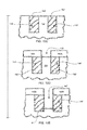
- FIG. 6 there is illustrated a top plan view of an opening of an interconnection component (not shown) in accordance with an embodiment, wherein the opening 610 extends between the first and second surfaces of a substrate (not shown).
- the opening 610 may have an oval shape when viewed from the top surface (not shown) of an interconnection component (not shown).
- the opening 610 may include any shape of conductor disclosed herein.
- a plurality of coaxial conductors 616 A, 616 B, 616 C extend along a central portion of the opening 610 ; none extend along a sidewall 612 of the opening 610 .
- the space that is not occupied by the coaxial conductors 616 is filled with an insulating or dielectric layer 632 .
- the dielectric layer can be a low-K dielectric layer, e.g., having a dielectric constant K of less than 3.5, such as may be various polymeric materials. In some embodiments, this can reduce coupling of signals between conductors within the opening, thus reducing unwanted effects such as cross-talk.
- the dielectric layer 632 may further include voids, e.g., gas-filled or evacuated regions or pores within the material.
- voids or air pores 634 can be disposed within the insulating region that extends within the opening 610 and around each of the coaxial conductors 616 A-C.
- the sizes of the voids, e.g., pores, can vary randomly. Average sizes of the voids can vary by design. Thus, in one example, the average sizes of the voids can be rather small, such as 1-2 nanometers in diameter. In other examples, the average sizes of the voids can range from about 10 nanometers to 100 nanometers. In a particular example, the average sizes of the voids can be about 20 nanometers and above.
- porogen as the dielectric layer can generate pores when processed.
- Some of the air pores will be essentially empty.
- the pores may be in a vacuum.
- Liquid crystal materials which are self-assembly materials are such an example.
- the dielectric layer 632 A between the inner and outer conductive portions of the coaxial conductors 616 can be the same as or different from dielectric layer 632 .
- the conductors within an opening there may be two coaxial conductors 616 A′, 616 C′ and a solid central conductor 616 B.
- the opening may be non-circular shaped and the solid central conductor 616 B may be positioned between the two coaxial conductors 616 A′, 616 C′, so that both the solid central conductor and the coaxial conductors are aligned and extend across the central portion of the opening 610 .
- FIG. 6A there may be two coaxial conductors 616 A′, 616 C′ and a solid central conductor 616 B.
- the opening may be non-circular shaped and the solid central conductor 616 B may be positioned between the two coaxial conductors 616 A′, 616 C′, so that both the solid central conductor and the coaxial conductors are aligned and extend across the central portion of the opening 610 .
- opposed coaxial conductive elements 616 D, 616 E each having a conductive core and a sheath as described above, may have surfaces extending along a well of the opening 610 , and opposed solid (or non-coaxial) conductors 616 F, 616 G may extend along the wall of the opening 610 at opposed locations spaced apart from the coaxial conductive elements 616 , 616 E.
- cross-sectional dimensions of the conductors in any of the embodiments described above can be the same, or can be different.
- any of the aforementioned interconnection components may be joined and electrically connected with other devices at either or both ends of the conductors.
- a first microelectronic element 756 A has bond pads 758 exposed at a front face thereof that faces the first surface 706 of the substrate 704 .
- the microelectronic element 756 A can be joined to bonding material, such as solder 734 , exposed at the first ends 718 of the conductors 716 A, 716 B.
- Second and third microelectronic elements 756 B, 756 C may be similarly joined to solder 734 positioned at the second ends 719 A of conductors 716 A, and second ends 719 B of conductors 716 B.
- first microelectronic element 756 A may contact only conductor 716 A, and a fourth microelectronic element 756 D may be provided at the second end of the conductors that have bond pads facing the first surface of the substrate.
- the contacts of the second microelectronic elements may be joined to corresponding ones of the second contacts through masses of bond material. It is to be appreciated that the first and second microelectronic element need not both be active chips, but may be passive components.
- interconnection components having one or more openings and a plurality of conductors within the one or more openings can be made in accordance with one or more of the above-described embodiments or by combining principles from one or more of the above-described embodiments. It is intended that the structures of any of the above-described embodiments can be combined to the fullest extent possible.
- the interconnection component can be incorporated in a microelectronic package or an assembly including a microelectronic element or a microelectronic package in any configuration.
- the shape and size of the opening in the substrate may vary, as well as the shape and size and placement of conductors within the opening.
- the conductor may have a cross-section that is round, oval, rectangular, or any other desirable shape.
- the conductors may be a coaxial conductor, and positioned adjacent the sidewall or away from the sidewall.
- the conductors may be staggered or aligned, or placed in any desirable configuration.
- FIGS. 8-8H in one embodiment of a method of making the interconnection component 100 shown in FIG. 1 , a cross-sectional portion of a substrate 104 is shown.
- a substrate 104 having a first surface 106 which typically is a major surface of the substrate, is shown with a first resist material 140 patterned thereon.
- the first resist material 140 may be comprised of resist materials known in the art.
- the first resist material 140 may be patterned to provide resist openings 142 or recesses within the first resist material 140 .
- the substrate 104 may be patterned to provide a corresponding opening 110 in the substrate that is aligned with the opening in the resist material.
- the substrate recess 110 can be created using known processes, such as etching, milling, wet or dry blasting, ablation or other techniques.
- the first resist material 140 may then be removed from the substrate 104 and a barrier or adhesion layer and seed layer coating 144 may be provided on the exposed surfaces of the substrate 104 .
- a second resist material 145 may be deposited into the opening 110 within the substrate 104 , as well as onto the first surface 106 of the substrate 104 .
- the second resist material 146 is then patterned to provide a columnar resist pillar 148 within opening 110 . (See FIG. 8D .)
- the patterning of the second resist material 146 will further provide one or more voids 150 A-D or cavities within the opening 110 , as also shown in FIG. 8E , a top view of the patterned resist and the resulting cavities.
- a metal 152 may then be plated or otherwise deposited into voids 150 A- 150 D in the opening 110 that are not occupied by resist pillar 148 , as shown in FIG. 8F .
- FIGS. 8G and 8H (as well as FIG.
- the resist pillar 148 may be removed to expose metal conductors 116 D, 116 E extending along at least a portion of the sidewall 112 of the openings 110 .
- the deposited metal 152 overlying the first surface 106 can be removed where necessary by subsequent processing, such as etching, ablation, grinding, lapping or polishing.
- the second surface (not shown) of the substrate 104 may be patterned to provide for an opening at the second surface (not shown) of the substrate 104 .
- FIGS. 9-9C a method for constructing an interconnection component with conductors in an opening that project beyond one or more surfaces of the substrate, such as the conductors described in FIG. 2 , is shown.
- the resist may be patterned to provide a resist pillar 148 within opening 110 , as well as resist pattern 146 on the first surface 106 of the substrate 104 .
- the resist pattern 146 is spaced away from the outer peripheral edge 114 of the opening 110 .
- a metal is plated or otherwise deposited within one or more openings defined by the patterned resist material 146 , 148 .
- the resist pillar 148 and resist pattern 146 on the first surface 106 of the substrate 104 can be removed to provide first and second conductors 116 A, 116 B projecting above the first surface 106 of the substrate 104 , as well as third and fourth conductors (not shown).
- a wettable layer 122 FIG. 9C
- Bonding material may then be provided over the wettable layer 122 of the conductors 116 A, 116 B.
- an opening may be provided through the second surface (not shown) of the substrate (not shown) to provide a through via.
- FIGS. 10-10I an alternative embodiment is described for forming an interconnection component, such as interconnection component 100 (see FIG. 1 ).
- a substrate 104 ′ is shown with a first mask 140 ′ patterned on the first surface 106 ′ of the substrate 104 ′.
- the patterning of the mask 140 ′ can include patterning openings 142 ′ in a layer of photoresist.
- the substrate 104 ′ may be patterned to provide openings 110 ′ in the substrate that are aligned with the openings 142 ′ in the mask.
- a seed layer 144 and/or an adhesion barrier layer may be provided over the exposed surfaces 141 ′ of the patterned substrate.
- the substrate opening 110 ′ may then be filled with a plated metal 152 ′, as shown in FIG. 10B .
- the plated metal 152 ′ may overlie the exposed surfaces 105 of the substrate 104 ′.
- the resulting structure may then be planarized, e.g., by grinding, lapping or polishing, as shown in FIG. 10C , so that at least one surface of the plated metal 152 ′ and one surface of the substrate 104 ′ are substantially co-planar. This can also result in the formation of conductors 116 ′. Referring to FIG.
- a second mask material 140 A e.g., a photoresist
- the substrate 104 may be again patterned to form a second resist opening 147 between the conductors 116 .
- FIG. 10E a portion of the substrate 104 extending below the second resist opening 147 and between the conductors 116 may then be patterned to leave only a residual portion P of substrate material remaining between the conductors 116 ′.
- a low K dielectric layer 132 ′ may be deposited on the substrate to fill the openings, as shown in FIG. 10F . This resulting structure may then be planarized, as shown in FIGS.
- FIG. 10I in an example of a structure so formed, a top view of the opening 110 ′ with conductors 116 A′, 116 B′, 116 C′, 116 D′ and a low K dielectric layer 132 ′ is shown. It is to be appreciated that the patterning of the first and second masks and the conductors 116 can be provided to result in any number of conductor configurations, such as those previously discussed in FIGS. 1-8 .
- FIGS. 11-11C illustrate one embodiment of a method of forming an interconnection component having openings with conductors extending therethrough, such as shown in FIG. 3 .
- the steps of patterning a resist mask on the substrate 304 ; providing corresponding openings 143 in the substrate 304 ; and providing a barrier layer 344 overlying the substrate 304 have been accomplished.
- another resist mask overlying the substrate has been patterned to provide resist pillars 348 , 348 A and voids 350 .
- a central columnar resist pillar 348 A can extend from the base 310 A of the opening 310 in the substrate 304 .
- a metal 352 can be provided within the voids 350 created between each of the resist pillars 348 , 348 A.
- the metal 352 may be plated within the void 350 , but any means of providing metal 352 within the void 350 may be used.
- the resist pillars 348 are removed to expose metal conductors 316 extending along at least a portion of the sidewall 312 of the openings 310 .
- the second surface (not shown) of the substrate 304 including the base 310 A of the substrate may be patterned or removed. This will provide for the conductors to extend beyond the opposed surfaces of the substrate 304 .
- the resulting structure, shown in FIG. 11C is therefore a substrate with first and second surfaces having conductors with first and second ends extending beyond the first and second surfaces of the substrate.
- Interconnection component 1000 includes a substrate or element 1004 with a first surface 1006 and a second surface 1008 .
- substrate 1004 includes substrate base 1003 and dielectric layers 1032 provided at the outermost portions of substrate base 1003 .
- the presence of a dielectric layer 1032 as part of the substrate is optional and largely depends on the material selected for the substrate base 1003 . If the substrate base 1003 possesses insulative properties, it may be unnecessary to provide an additional dielectric layer 1032 .
- substrate 1004 is primarily a low CTE substrate comprised of semiconductor material, e.g., silicon, glass, or ceramic material or liquid crystal polymer material, among others.
- Substrate 1004 also has a thickness T as previously disclosed herein.
- One or more openings 1010 extend between the first surface 1006 and second surface 1008 of the substrate 1004 .
- One or more of the openings 1010 may have a circular cross-section. (See also FIG. 14C .)
- the openings 1010 have a diameter D ranging from 0.5-50 microns.
- one or more conductors 1016 can extend through the openings 1010 .
- the conductors 1016 extend along and through the length of the openings 1010 .
- the conductors 1016 are spaced apart from one another so that they do not contact one another.
- the opening 1010 may be filled with an intermediate dielectric layer, as previously disclosed herein.
- First ends 1018 of the conductors 1016 extend onto the first surface 1006 and second surface 1008 of the substrate 1004 .
- first ends 1018 of the conductors 1016 may be flat pads having a semi-circular shape, although conductors 1016 can be patterned to take on any desired shape.
- this embodiment is similar to the embodiment shown in FIG. 12 , and differs with respect to the shape of the openings 1110 extending through the substrate 1104 and the arrangement of conductors 1116 within the opening. As in the previous embodiment, four conductors 1116 are shown extending through openings 1110 . First ends 1118 of the conductors 1116 extend onto the first surface 1106 of the substrate 1104 and second ends 1119 extend onto the second surface 1108 . As will be discussed in greater detail (see FIG.
- one or more of the openings 1110 is comprised of a central circular cylindrical opening 1180 having a circumferential edge 1117 and a series of circular cylindrical peripheral openings 1180 A, 1180 B, 1180 C, 1180 D that overlap the circumferential edge 1117 of the central opening 1180 .
- One or more of the openings 1180 may also be spaced apart from one another along the circumferential edge 1117 of the central circular opening 1180 .
- Each of the openings 1110 and peripheral openings 1180 A, 1180 B, 1180 C, 1180 D extend through a thickness of the substrate 1104 and at least some of the conductors extend along inner surfaces of the peripheral openings 1180 A, 1180 B, 1180 C, 1180 D.
- FIGS. 14-14B respectively a perspective view, top plan view, and cross-sectional view of substrate base 1003 taken along line 14 B- 14 B in FIG. 14 .
- substrate base 1003 is provided with openings 1010 that have a circular cross-section and that extend between the first surface 1007 and second surface 1009 of the substrate base 1003 .
- Each opening 1010 has an interior surface 1068 ( FIG. 14C ) and outer circumferential edges 1017 at the first surface 1007 and second surface 1009 of the substrate base 1003 .
- a dielectric layer 1032 may be provided on the exposed surfaces of substrate base 1003 to form substrate 1004 .
- dielectric layer 1032 is provided on first surface 1007 and second surface 1009 of the substrate base 1003 .
- dielectric layer 1032 may be provided within each of the interior surfaces 1068 of openings 1010 in the substrate.
- Dielectric layer 1032 also has an exposed outer surface 1035 at this stage of the process. It is to be understood that providing a dielectric layer 1032 is an optional step.
- a dielectric layer 1032 will largely depend upon the material selected for the substrate base 1003 . In one example, a dielectric layer 1032 will be unnecessary if the underlying substrate base 1003 is comprised of a non-conductive material such as glass.
- a resist layer 1084 may be provided over the outer surface 1033 ( FIG. 14D ) of dielectric layer 1032 . Resist layer 1084 will overlie first and second surfaces 1006 , 1008 of the substrate 1004 , which also directly overlie the outer surface 1033 of dielectric layer 1032 . As best seen in FIG. 14F , resist material will also fill (either fully or partially) openings 1010 .
- mask 1070 has a plurality of groups of openings 1071 .
- Each group may include four circular openings 1071 A-D that together form the shape of a diamond. It is to be appreciated that each of the openings 1071 A-D can have alternative shapes, such as triangular, that can be based on a particular design. Additionally, each opening 1071 A-D can be the same shape or one or more of the openings 1071 A-D can differ. Furthermore, each group 1071 of openings may consist of only one opening, or more than one opening.
- the mask 1070 may be temporarily placed onto the exposed surfaces 1085 of resist layer 1084 (see FIG. 14F ) so that the openings 1071 in the mask 1070 will overlap the underlying openings 1010 that have been covered by resist layer 1084 and/or filled with resist material from the resist layer 1084 .
- openings 1086 can be created in the resist layer 1084 , as well as through the resist layer 1084 by using the mask and mask openings 1071 as a template.
- portions of the resist material overlying the dielectric layer 1032 can be removed using etching, particle blasting, or known methods of removal. Additionally, using the same or similar methods, resist material that both fills the openings 1010 and is exposed through the opening 1086 created in the resist layer can be removed.
- the resist layer 1084 is made from a material significantly softer than the dielectric material comprising the dielectric layer 1032 so as to aid in the resist material removal process.
- a barrier or seed layer 1087 may be coated onto the portions of dielectric layer 1032 that are now exposed within each of the openings 1010 .
- a metal may then be plated onto the barrier/seed layer 1087 to form conductors 1016 , as shown in FIGS. 14M-N .
- any remaining resist material from resist layer 1084 may be removed, resulting in the interconnection component of FIG. 12A .
- a substrate base 1103 includes a plurality of openings 1110 .
- the openings 1110 may be made from a series of central openings 1180 overlapped by one or more other openings.
- FIG. 15 In the exemplary embodiment shown in FIG.
- the cross-section of the opening 1110 includes a central opening 1180 having a circular cross-sectional circumferential edge 1117 and a series of four overlapping openings 1180 A, 1180 B, 1180 C, and 1180 D that each have circular cross-sections.
- the overlapping openings 1180 A-D extend around the circumferential edge 1117 of the central opening 1180 .
- Each of the four circular overlapping openings 1180 A-D have respective outer edges 1181 A-D that extend around the circumferential edge 1181 of the central opening 1180 . As shown, only those portions of circumferential edge 1117 of the central opening 1180 that are not overlapped by the overlapping openings 1180 A-D remain visible.
- circular openings are provided around the circumferential edge 1117 of the central circular opening 1180 , additional shapes such as a rounded square, a circle with more than one small overlapping circle (as shown), triangular, or any other desired shape may be provided.
- the shape of the central opening 1180 may also differ.
- the substrate 1104 may include a coating of dielectric layer 1132 , as shown in FIG. 15C and FIG. 15D (a cross-sectional view taken along line 15 D- 14 D of FIG. 15C ).
- dielectric layer 1132 is provided over the exposed first and second surfaces 1107 , 1109 of the substrate base 1103 , as well as within the openings 1110 extending between the first and second surfaces 1107 , 1109 .
- a seed layer 1187 may be provided over the outer surface 1135 ( FIG. 15D ) of the dielectric layer 1132 overlying the first and second surfaces 1107 , 1109 of the substrate base 1103 , as well as the dielectric layer 1132 lining the openings 1110 .
- a resist layer 1184 may be provided over the seed layer 1187 that overlies the first and second surfaces 1107 , 1109 of the substrate base 1103 , as well as within the openings 1110 lined by seed layers 1187 .
- the resist layer 1184 substantially fills all of the openings 1110 with resist material, such that the openings 1110 are filled with resist material.
- FIG. 15I and FIG. 15J (a cross-sectional view taken along line 15 J- 15 J of FIG. 15I )
- the resist layer 1184 overlying the first surface 1107 and second surface 1109 of the substrate base 1103 may be selectively etched or patterned to provide openings 1186 within the resist layer 1184 that overlie portions of the seed layer 1187 .
- the opening 1186 created in the resist layer 1184 may be shaped similarly to the original shape of the opening 1110 created in the substrate base 1103 .
- the opening 1186 created in the resist layer 1184 overlaying has a circular central resist opening 1180 ′ that is aligned with the central opening 1180 extending through the substrate 1104 .
- Four circular resist openings 1180 A′, 1180 B′, 1180 C′, 1180 D′ overlap and extend around the circumferential edge 1181 of the central resist opening 1180 ′.
- the overlapping circular resist openings 1180 A- 1180 D of the resist layer 1184 are not aligned with the overlapping openings 1180 A- 1180 D in the substrate base 1103 .
- the overlapping circular resist openings 1180 A′- 1180 D′ are instead positioned directly adjacent and between each of the overlapping openings 1180 A- 1180 D in the substrate base 1103 , as shown in broken line FIG. 15I . It is to be appreciated that second surfaces may be patterned identical to the first surface.
- the resist material filling the central portion of the opening 1110 in the substrate 1104 can also be selectively etched so as to expose the seed layer overlying the circumferential edge 1117 of the opening extending through the substrate 1104 .
- FIG. 15K and FIG. 15L (a cross-sectional view taken along line 15 L- 15 L of FIG. 15K ), a metal material, such as copper, copper alloys or the like may be plated up over the seed layer 1187 , that is exposed through the openings 1186 in the resist layer 1184 to form conductors 1116 .
- a metal material such as copper, copper alloys or the like may be plated up over the seed layer 1187 , that is exposed through the openings 1186 in the resist layer 1184 to form conductors 1116 .
- FIG. 15M and FIG. 15N (a cross-sectional view taken along line 15 N- 15 N of FIG. 15M )
- all of the remaining resist layers 1184 can be removed, including any remaining resist material within the overlapping openings 1180 A- 1180 D, to reveal the underlying seed layer 1187 . Thereafter, the remaining portions of seed layer 1187 may be removed to reveal the interconnection component of FIG. 13 .
- FIGS. 16-16G a method of making the interconnection component 1100 in accordance with an alternative embodiment is shown.
- a substrate base 1103 ′ identical to the substrate base 1103 of FIG. 15 a dielectric layer 1132 ′ is again provided over the exposed surfaces 1107 ′, 1109 ′ of the substrate base 1103 ′, as well as within the openings 1110 ′.
- a resist layer 1184 ′ is then provided on the exposed surfaces 1135 ′ of dielectric layer 1132 ′ second within openings 1110 ′ As shown, the dielectric layer 1132 ′ within openings 1110 ′ is exposed through the openings 1110 ′ in the resist layer 1184 ′.
- FIG. 16B and FIG. 16C (a cross-sectional view taken along line 16 C- 16 C of FIG. 16B ), using the openings 1186 ′ as a mask, a seed/barrier material 1187 ′ may then be provided on the first and second surfaces 1106 ′, 1108 ′ of the dielectric layer 1132 and within the openings 1110 ′.
- FIG. 16D- and FIG. 16E (a cross-sectional view taken along line 16 E- 16 E of FIG. 16D ), a metal may be provided over the exposed portion of the seed/barrier layer 1187 ′ to create conductors 1116 ′.
- FIG. 16F and FIG. 16G (a cross-sectional view taken along line 16 G- 16 G of FIG.
- resist material that fills the openings 1110 ′ in the substrates may be removed, such as by selective etching. This provides for openings that are similar to the openings shown in FIG. 15M , but created by a different process.
- the resist layer 1184 ′ may then be removed to reveal the interconnection element 1100 of FIG. 13 . Preparing the interconnection component in this manner eliminates the step of having to remove the seed layer, and only requires removal of the resist layer.
Abstract
Description
Claims (36)
Priority Applications (3)
| Application Number | Priority Date | Filing Date | Title |
|---|---|---|---|
| US13/296,785 US8916781B2 (en) | 2011-11-15 | 2011-11-15 | Cavities containing multi-wiring structures and devices |
| US14/573,461 US10015881B2 (en) | 2011-11-15 | 2014-12-17 | Cavities containing multi-wiring structures and devices |
| US16/007,410 US10813214B2 (en) | 2011-11-15 | 2018-06-13 | Cavities containing multi-wiring structures and devices |
Applications Claiming Priority (1)
| Application Number | Priority Date | Filing Date | Title |
|---|---|---|---|
| US13/296,785 US8916781B2 (en) | 2011-11-15 | 2011-11-15 | Cavities containing multi-wiring structures and devices |
Related Child Applications (1)
| Application Number | Title | Priority Date | Filing Date |
|---|---|---|---|
| US14/573,461 Division US10015881B2 (en) | 2011-11-15 | 2014-12-17 | Cavities containing multi-wiring structures and devices |
Publications (2)
| Publication Number | Publication Date |
|---|---|
| US20130122747A1 US20130122747A1 (en) | 2013-05-16 |
| US8916781B2 true US8916781B2 (en) | 2014-12-23 |
Family
ID=48281068
Family Applications (3)
| Application Number | Title | Priority Date | Filing Date |
|---|---|---|---|
| US13/296,785 Active 2032-07-05 US8916781B2 (en) | 2011-11-15 | 2011-11-15 | Cavities containing multi-wiring structures and devices |
| US14/573,461 Active 2033-10-25 US10015881B2 (en) | 2011-11-15 | 2014-12-17 | Cavities containing multi-wiring structures and devices |
| US16/007,410 Active 2032-09-17 US10813214B2 (en) | 2011-11-15 | 2018-06-13 | Cavities containing multi-wiring structures and devices |
Family Applications After (2)
| Application Number | Title | Priority Date | Filing Date |
|---|---|---|---|
| US14/573,461 Active 2033-10-25 US10015881B2 (en) | 2011-11-15 | 2014-12-17 | Cavities containing multi-wiring structures and devices |
| US16/007,410 Active 2032-09-17 US10813214B2 (en) | 2011-11-15 | 2018-06-13 | Cavities containing multi-wiring structures and devices |
Country Status (1)
| Country | Link |
|---|---|
| US (3) | US8916781B2 (en) |
Cited By (24)
| Publication number | Priority date | Publication date | Assignee | Title |
|---|---|---|---|---|
| US9490222B1 (en) | 2015-10-12 | 2016-11-08 | Invensas Corporation | Wire bond wires for interference shielding |
| US9735084B2 (en) | 2014-12-11 | 2017-08-15 | Invensas Corporation | Bond via array for thermal conductivity |
| US9761554B2 (en) | 2015-05-07 | 2017-09-12 | Invensas Corporation | Ball bonding metal wire bond wires to metal pads |
| US9842745B2 (en) | 2012-02-17 | 2017-12-12 | Invensas Corporation | Heat spreading substrate with embedded interconnects |
| US9852969B2 (en) | 2013-11-22 | 2017-12-26 | Invensas Corporation | Die stacks with one or more bond via arrays of wire bond wires and with one or more arrays of bump interconnects |
| US9888579B2 (en) | 2015-03-05 | 2018-02-06 | Invensas Corporation | Pressing of wire bond wire tips to provide bent-over tips |
| US9911718B2 (en) | 2015-11-17 | 2018-03-06 | Invensas Corporation | ‘RDL-First’ packaged microelectronic device for a package-on-package device |
| US9935075B2 (en) | 2016-07-29 | 2018-04-03 | Invensas Corporation | Wire bonding method and apparatus for electromagnetic interference shielding |
| US9953914B2 (en) | 2012-05-22 | 2018-04-24 | Invensas Corporation | Substrate-less stackable package with wire-bond interconnect |
| US9984992B2 (en) | 2015-12-30 | 2018-05-29 | Invensas Corporation | Embedded wire bond wires for vertical integration with separate surface mount and wire bond mounting surfaces |
| US10008477B2 (en) | 2013-09-16 | 2018-06-26 | Invensas Corporation | Microelectronic element with bond elements to encapsulation surface |
| US10008469B2 (en) | 2015-04-30 | 2018-06-26 | Invensas Corporation | Wafer-level packaging using wire bond wires in place of a redistribution layer |
| US10026717B2 (en) | 2013-11-22 | 2018-07-17 | Invensas Corporation | Multiple bond via arrays of different wire heights on a same substrate |
| US10062661B2 (en) | 2011-05-03 | 2018-08-28 | Tessera, Inc. | Package-on-package assembly with wire bonds to encapsulation surface |
| US10128216B2 (en) | 2010-07-19 | 2018-11-13 | Tessera, Inc. | Stackable molded microelectronic packages |
| US10181457B2 (en) | 2015-10-26 | 2019-01-15 | Invensas Corporation | Microelectronic package for wafer-level chip scale packaging with fan-out |
| US10297582B2 (en) | 2012-08-03 | 2019-05-21 | Invensas Corporation | BVA interposer |
| US10299368B2 (en) | 2016-12-21 | 2019-05-21 | Invensas Corporation | Surface integrated waveguides and circuit structures therefor |
| US10332854B2 (en) | 2015-10-23 | 2019-06-25 | Invensas Corporation | Anchoring structure of fine pitch bva |
| US10381326B2 (en) | 2014-05-28 | 2019-08-13 | Invensas Corporation | Structure and method for integrated circuits packaging with increased density |
| US10460958B2 (en) | 2013-08-07 | 2019-10-29 | Invensas Corporation | Method of manufacturing embedded packaging with preformed vias |
| US10490528B2 (en) | 2015-10-12 | 2019-11-26 | Invensas Corporation | Embedded wire bond wires |
| US10529636B2 (en) | 2014-01-17 | 2020-01-07 | Invensas Corporation | Fine pitch BVA using reconstituted wafer with area array accessible for testing |
| US10756049B2 (en) | 2011-10-17 | 2020-08-25 | Invensas Corporation | Package-on-package assembly with wire bond vias |
Families Citing this family (6)
| Publication number | Priority date | Publication date | Assignee | Title |
|---|---|---|---|---|
| US10886250B2 (en) | 2015-07-10 | 2021-01-05 | Invensas Corporation | Structures and methods for low temperature bonding using nanoparticles |
| US10515913B2 (en) | 2017-03-17 | 2019-12-24 | Invensas Bonding Technologies, Inc. | Multi-metal contact structure |
| US10446441B2 (en) | 2017-06-05 | 2019-10-15 | Invensas Corporation | Flat metal features for microelectronics applications |
| US10790262B2 (en) | 2018-04-11 | 2020-09-29 | Invensas Bonding Technologies, Inc. | Low temperature bonded structures |
| WO2020131897A1 (en) * | 2018-12-17 | 2020-06-25 | Averatek Corporation | Three dimensional circuit formation |
| US11735523B2 (en) | 2020-05-19 | 2023-08-22 | Adeia Semiconductor Bonding Technologies Inc. | Laterally unconfined structure |
Citations (17)
| Publication number | Priority date | Publication date | Assignee | Title |
|---|---|---|---|---|
| US3702284A (en) * | 1968-12-04 | 1972-11-07 | Siemens Ag | Process of producing plated through-hole printed circuit boards |
| US4636919A (en) * | 1985-03-20 | 1987-01-13 | Hitachi, Ltd. | Multilayer printed circuit board |
| US5133669A (en) * | 1990-07-23 | 1992-07-28 | Northern Telecom Limited | Circuit board pins |
| US5340947A (en) * | 1992-06-22 | 1994-08-23 | Cirqon Technologies Corporation | Ceramic substrates with highly conductive metal vias |
| US5528000A (en) * | 1993-08-18 | 1996-06-18 | Shipley Company, L.L.C. | Electroplating process and composition |
| US5541567A (en) * | 1994-10-17 | 1996-07-30 | International Business Machines Corporation | Coaxial vias in an electronic substrate |
| US6479764B1 (en) * | 2000-05-10 | 2002-11-12 | International Business Machines Corporation | Via structure with dual current path |
| US20020166688A1 (en) * | 1996-05-02 | 2002-11-14 | Tessera, Inc. | Microelectronic connections with liquid conductive elements |
| US6753480B2 (en) * | 2001-10-12 | 2004-06-22 | Ultratera Corporation | Printed circuit board having permanent solder mask |
| US6927346B2 (en) * | 2002-12-20 | 2005-08-09 | Intel Corporation | Surface mount technology to via-in-pad interconnections |
| US7282784B2 (en) * | 2004-08-31 | 2007-10-16 | Micron Technology, Inc. | Methods of manufacture of a via structure comprising a plurality of conductive elements and methods of forming multichip modules including such via structures |
| US20070258173A1 (en) * | 2006-05-08 | 2007-11-08 | Houfei Chen | Substrates, systems, and devices including structures for suppressing power and ground plane noise, and methods for suppressing power and ground plane noise |
| US20080078572A1 (en) * | 2006-08-31 | 2008-04-03 | Honda Motor Co., Ltd. | Circuit board and method of manufacturing the same |
| US7535093B1 (en) * | 2002-03-08 | 2009-05-19 | Raytheon Company | Method and apparatus for packaging circuit devices |
| US20100163296A1 (en) * | 2008-12-31 | 2010-07-01 | Industrial Technology Research Institute | Structure of multiple coaxial leads within single via in substrate and manufacturing method thereof |
| US20100236823A1 (en) * | 2009-03-18 | 2010-09-23 | Sun Microsystems, Inc. | Ring of power via |
| US20120313239A1 (en) | 2011-06-13 | 2012-12-13 | Tessera, Inc. | Flip chip assembly and process with sintering material on metal bumps |
Family Cites Families (6)
| Publication number | Priority date | Publication date | Assignee | Title |
|---|---|---|---|---|
| US3400210A (en) * | 1966-04-26 | 1968-09-03 | Automatic Elect Lab | Interlayer connection technique for multilayer printed wiring boards |
| US4543715A (en) * | 1983-02-28 | 1985-10-01 | Allied Corporation | Method of forming vertical traces on printed circuit board |
| US5619791A (en) * | 1994-06-30 | 1997-04-15 | Lucent Technologies Inc. | Method for fabricating highly conductive vias |
| US6659328B2 (en) * | 2001-12-18 | 2003-12-09 | Xerox Corporation | Method and apparatus for deposition of solder paste for surface mount components on a printed wiring board |
| US6891272B1 (en) * | 2002-07-31 | 2005-05-10 | Silicon Pipe, Inc. | Multi-path via interconnection structures and methods for manufacturing the same |
| TWI231731B (en) * | 2003-12-18 | 2005-04-21 | Advanced Semiconductor Eng | Substrate with micro via structures by laser technique |
-
2011
- 2011-11-15 US US13/296,785 patent/US8916781B2/en active Active
-
2014
- 2014-12-17 US US14/573,461 patent/US10015881B2/en active Active
-
2018
- 2018-06-13 US US16/007,410 patent/US10813214B2/en active Active
Patent Citations (17)
| Publication number | Priority date | Publication date | Assignee | Title |
|---|---|---|---|---|
| US3702284A (en) * | 1968-12-04 | 1972-11-07 | Siemens Ag | Process of producing plated through-hole printed circuit boards |
| US4636919A (en) * | 1985-03-20 | 1987-01-13 | Hitachi, Ltd. | Multilayer printed circuit board |
| US5133669A (en) * | 1990-07-23 | 1992-07-28 | Northern Telecom Limited | Circuit board pins |
| US5340947A (en) * | 1992-06-22 | 1994-08-23 | Cirqon Technologies Corporation | Ceramic substrates with highly conductive metal vias |
| US5528000A (en) * | 1993-08-18 | 1996-06-18 | Shipley Company, L.L.C. | Electroplating process and composition |
| US5541567A (en) * | 1994-10-17 | 1996-07-30 | International Business Machines Corporation | Coaxial vias in an electronic substrate |
| US20020166688A1 (en) * | 1996-05-02 | 2002-11-14 | Tessera, Inc. | Microelectronic connections with liquid conductive elements |
| US6479764B1 (en) * | 2000-05-10 | 2002-11-12 | International Business Machines Corporation | Via structure with dual current path |
| US6753480B2 (en) * | 2001-10-12 | 2004-06-22 | Ultratera Corporation | Printed circuit board having permanent solder mask |
| US7535093B1 (en) * | 2002-03-08 | 2009-05-19 | Raytheon Company | Method and apparatus for packaging circuit devices |
| US6927346B2 (en) * | 2002-12-20 | 2005-08-09 | Intel Corporation | Surface mount technology to via-in-pad interconnections |
| US7282784B2 (en) * | 2004-08-31 | 2007-10-16 | Micron Technology, Inc. | Methods of manufacture of a via structure comprising a plurality of conductive elements and methods of forming multichip modules including such via structures |
| US20070258173A1 (en) * | 2006-05-08 | 2007-11-08 | Houfei Chen | Substrates, systems, and devices including structures for suppressing power and ground plane noise, and methods for suppressing power and ground plane noise |
| US20080078572A1 (en) * | 2006-08-31 | 2008-04-03 | Honda Motor Co., Ltd. | Circuit board and method of manufacturing the same |
| US20100163296A1 (en) * | 2008-12-31 | 2010-07-01 | Industrial Technology Research Institute | Structure of multiple coaxial leads within single via in substrate and manufacturing method thereof |
| US20100236823A1 (en) * | 2009-03-18 | 2010-09-23 | Sun Microsystems, Inc. | Ring of power via |
| US20120313239A1 (en) | 2011-06-13 | 2012-12-13 | Tessera, Inc. | Flip chip assembly and process with sintering material on metal bumps |
Cited By (41)
| Publication number | Priority date | Publication date | Assignee | Title |
|---|---|---|---|---|
| US10128216B2 (en) | 2010-07-19 | 2018-11-13 | Tessera, Inc. | Stackable molded microelectronic packages |
| US11424211B2 (en) | 2011-05-03 | 2022-08-23 | Tessera Llc | Package-on-package assembly with wire bonds to encapsulation surface |
| US10062661B2 (en) | 2011-05-03 | 2018-08-28 | Tessera, Inc. | Package-on-package assembly with wire bonds to encapsulation surface |
| US10593643B2 (en) | 2011-05-03 | 2020-03-17 | Tessera, Inc. | Package-on-package assembly with wire bonds to encapsulation surface |
| US11189595B2 (en) | 2011-10-17 | 2021-11-30 | Invensas Corporation | Package-on-package assembly with wire bond vias |
| US10756049B2 (en) | 2011-10-17 | 2020-08-25 | Invensas Corporation | Package-on-package assembly with wire bond vias |
| US11735563B2 (en) | 2011-10-17 | 2023-08-22 | Invensas Llc | Package-on-package assembly with wire bond vias |
| US9842745B2 (en) | 2012-02-17 | 2017-12-12 | Invensas Corporation | Heat spreading substrate with embedded interconnects |
| US9953914B2 (en) | 2012-05-22 | 2018-04-24 | Invensas Corporation | Substrate-less stackable package with wire-bond interconnect |
| US10510659B2 (en) | 2012-05-22 | 2019-12-17 | Invensas Corporation | Substrate-less stackable package with wire-bond interconnect |
| US10170412B2 (en) | 2012-05-22 | 2019-01-01 | Invensas Corporation | Substrate-less stackable package with wire-bond interconnect |
| US10297582B2 (en) | 2012-08-03 | 2019-05-21 | Invensas Corporation | BVA interposer |
| US10460958B2 (en) | 2013-08-07 | 2019-10-29 | Invensas Corporation | Method of manufacturing embedded packaging with preformed vias |
| US10008477B2 (en) | 2013-09-16 | 2018-06-26 | Invensas Corporation | Microelectronic element with bond elements to encapsulation surface |
| US10026717B2 (en) | 2013-11-22 | 2018-07-17 | Invensas Corporation | Multiple bond via arrays of different wire heights on a same substrate |
| US9852969B2 (en) | 2013-11-22 | 2017-12-26 | Invensas Corporation | Die stacks with one or more bond via arrays of wire bond wires and with one or more arrays of bump interconnects |
| US10629567B2 (en) | 2013-11-22 | 2020-04-21 | Invensas Corporation | Multiple plated via arrays of different wire heights on same substrate |
| US10290613B2 (en) | 2013-11-22 | 2019-05-14 | Invensas Corporation | Multiple bond via arrays of different wire heights on a same substrate |
| US10529636B2 (en) | 2014-01-17 | 2020-01-07 | Invensas Corporation | Fine pitch BVA using reconstituted wafer with area array accessible for testing |
| US11404338B2 (en) | 2014-01-17 | 2022-08-02 | Invensas Corporation | Fine pitch bva using reconstituted wafer with area array accessible for testing |
| US10381326B2 (en) | 2014-05-28 | 2019-08-13 | Invensas Corporation | Structure and method for integrated circuits packaging with increased density |
| US9735084B2 (en) | 2014-12-11 | 2017-08-15 | Invensas Corporation | Bond via array for thermal conductivity |
| US9888579B2 (en) | 2015-03-05 | 2018-02-06 | Invensas Corporation | Pressing of wire bond wire tips to provide bent-over tips |
| US10806036B2 (en) | 2015-03-05 | 2020-10-13 | Invensas Corporation | Pressing of wire bond wire tips to provide bent-over tips |
| US10008469B2 (en) | 2015-04-30 | 2018-06-26 | Invensas Corporation | Wafer-level packaging using wire bond wires in place of a redistribution layer |
| US9761554B2 (en) | 2015-05-07 | 2017-09-12 | Invensas Corporation | Ball bonding metal wire bond wires to metal pads |
| US10559537B2 (en) | 2015-10-12 | 2020-02-11 | Invensas Corporation | Wire bond wires for interference shielding |
| US10490528B2 (en) | 2015-10-12 | 2019-11-26 | Invensas Corporation | Embedded wire bond wires |
| US9812402B2 (en) | 2015-10-12 | 2017-11-07 | Invensas Corporation | Wire bond wires for interference shielding |
| US9490222B1 (en) | 2015-10-12 | 2016-11-08 | Invensas Corporation | Wire bond wires for interference shielding |
| US11462483B2 (en) | 2015-10-12 | 2022-10-04 | Invensas Llc | Wire bond wires for interference shielding |
| US10115678B2 (en) | 2015-10-12 | 2018-10-30 | Invensas Corporation | Wire bond wires for interference shielding |
| US10332854B2 (en) | 2015-10-23 | 2019-06-25 | Invensas Corporation | Anchoring structure of fine pitch bva |
| US10181457B2 (en) | 2015-10-26 | 2019-01-15 | Invensas Corporation | Microelectronic package for wafer-level chip scale packaging with fan-out |
| US9911718B2 (en) | 2015-11-17 | 2018-03-06 | Invensas Corporation | ‘RDL-First’ packaged microelectronic device for a package-on-package device |
| US10043779B2 (en) | 2015-11-17 | 2018-08-07 | Invensas Corporation | Packaged microelectronic device for a package-on-package device |
| US9984992B2 (en) | 2015-12-30 | 2018-05-29 | Invensas Corporation | Embedded wire bond wires for vertical integration with separate surface mount and wire bond mounting surfaces |
| US10325877B2 (en) | 2015-12-30 | 2019-06-18 | Invensas Corporation | Embedded wire bond wires for vertical integration with separate surface mount and wire bond mounting surfaces |
| US9935075B2 (en) | 2016-07-29 | 2018-04-03 | Invensas Corporation | Wire bonding method and apparatus for electromagnetic interference shielding |
| US10658302B2 (en) | 2016-07-29 | 2020-05-19 | Invensas Corporation | Wire bonding method and apparatus for electromagnetic interference shielding |
| US10299368B2 (en) | 2016-12-21 | 2019-05-21 | Invensas Corporation | Surface integrated waveguides and circuit structures therefor |
Also Published As
| Publication number | Publication date |
|---|---|
| US20180295718A1 (en) | 2018-10-11 |
| US10015881B2 (en) | 2018-07-03 |
| US10813214B2 (en) | 2020-10-20 |
| US20130122747A1 (en) | 2013-05-16 |
| US20150101858A1 (en) | 2015-04-16 |
Similar Documents
| Publication | Publication Date | Title |
|---|---|---|
| US10813214B2 (en) | Cavities containing multi-wiring structures and devices | |
| US9899298B2 (en) | Microelectronic packages having mold-embedded traces and methods for the production thereof | |
| TWI528519B (en) | Package and method for forming a transmission line | |
| US9331029B2 (en) | Microelectronic packages having mold-embedded traces and methods for the production thereof | |
| US9721920B2 (en) | Embedded chip packages and methods for manufacturing an embedded chip package | |
| US6781224B2 (en) | Semiconductor device and package including forming pyramid mount protruding through silicon substrate | |
| US9666930B2 (en) | Interface between a semiconductor die and a waveguide, where the interface is covered by a molding compound | |
| JP5397962B2 (en) | Method for forming a semiconductor device package | |
| US8093705B2 (en) | Dual face package having resin insulating layer | |
| KR101107858B1 (en) | Conductive pillar structure for semiconductor substrate and method of manufacture | |
| US9070674B2 (en) | Through-silicon coaxial via structure and method | |
| KR20080057190A (en) | 3d electronic packaging structure with enhanced grounding performance and embedded antenna | |
| US10159148B2 (en) | Porous alumina templates for electronic packages | |
| US9184113B1 (en) | Methods of forming coaxial feedthroughs for 3D integrated circuits | |
| US9025340B2 (en) | Devices and stacked microelectronic packages with in-trench package surface conductors and methods of their fabrication | |
| US9036363B2 (en) | Devices and stacked microelectronic packages with parallel conductors and intra-conductor isolator structures and methods of their fabrication | |
| JP2009049087A (en) | Method for manufacturing electronic component and electronic component | |
| US8385084B2 (en) | Shielding structures for signal paths in electronic devices | |
| TWI615933B (en) | Semiconductor device and method of manufacturing semiconductor device | |
| CN114823557A (en) | Fan-out type double-sided packaging structure and preparation method thereof | |
| US11705421B2 (en) | Apparatus including solder-core connectors and methods of manufacturing the same | |
| WO2008058474A1 (en) | Conductor polymer composite carrier with isoproperty conductive columns | |
| US20180122721A1 (en) | Plug structure of a semiconductor chip and method of manufacturing the same | |
| KR20100019634A (en) | Semiconductor device and fabricating method thereof |
Legal Events
| Date | Code | Title | Description |
|---|---|---|---|
| AS | Assignment |
Owner name: INVENSAS CORPORATION, CALIFORNIA Free format text: ASSIGNMENT OF ASSIGNORS INTEREST;ASSIGNORS:UZOH, CYPRIAN;MITCHELL, CRAIG;HABA, BELGACEM;AND OTHERS;SIGNING DATES FROM 20120117 TO 20120307;REEL/FRAME:028146/0684 |
|
| STCF | Information on status: patent grant |
Free format text: PATENTED CASE |
|
| AS | Assignment |
Owner name: ROYAL BANK OF CANADA, AS COLLATERAL AGENT, CANADA Free format text: SECURITY INTEREST;ASSIGNORS:INVENSAS CORPORATION;TESSERA, INC.;TESSERA ADVANCED TECHNOLOGIES, INC.;AND OTHERS;REEL/FRAME:040797/0001 Effective date: 20161201 |
|
| MAFP | Maintenance fee payment |
Free format text: PAYMENT OF MAINTENANCE FEE, 4TH YEAR, LARGE ENTITY (ORIGINAL EVENT CODE: M1551) Year of fee payment: 4 |
|
| AS | Assignment |
Owner name: BANK OF AMERICA, N.A., NORTH CAROLINA Free format text: SECURITY INTEREST;ASSIGNORS:ROVI SOLUTIONS CORPORATION;ROVI TECHNOLOGIES CORPORATION;ROVI GUIDES, INC.;AND OTHERS;REEL/FRAME:053468/0001 Effective date: 20200601 |
|
| AS | Assignment |
Owner name: DTS LLC, CALIFORNIA Free format text: RELEASE BY SECURED PARTY;ASSIGNOR:ROYAL BANK OF CANADA;REEL/FRAME:052920/0001 Effective date: 20200601 Owner name: INVENSAS BONDING TECHNOLOGIES, INC. (F/K/A ZIPTRONIX, INC.), CALIFORNIA Free format text: RELEASE BY SECURED PARTY;ASSIGNOR:ROYAL BANK OF CANADA;REEL/FRAME:052920/0001 Effective date: 20200601 Owner name: TESSERA ADVANCED TECHNOLOGIES, INC, CALIFORNIA Free format text: RELEASE BY SECURED PARTY;ASSIGNOR:ROYAL BANK OF CANADA;REEL/FRAME:052920/0001 Effective date: 20200601 Owner name: IBIQUITY DIGITAL CORPORATION, MARYLAND Free format text: RELEASE BY SECURED PARTY;ASSIGNOR:ROYAL BANK OF CANADA;REEL/FRAME:052920/0001 Effective date: 20200601 Owner name: PHORUS, INC., CALIFORNIA Free format text: RELEASE BY SECURED PARTY;ASSIGNOR:ROYAL BANK OF CANADA;REEL/FRAME:052920/0001 Effective date: 20200601 Owner name: INVENSAS CORPORATION, CALIFORNIA Free format text: RELEASE BY SECURED PARTY;ASSIGNOR:ROYAL BANK OF CANADA;REEL/FRAME:052920/0001 Effective date: 20200601 Owner name: TESSERA, INC., CALIFORNIA Free format text: RELEASE BY SECURED PARTY;ASSIGNOR:ROYAL BANK OF CANADA;REEL/FRAME:052920/0001 Effective date: 20200601 Owner name: DTS, INC., CALIFORNIA Free format text: RELEASE BY SECURED PARTY;ASSIGNOR:ROYAL BANK OF CANADA;REEL/FRAME:052920/0001 Effective date: 20200601 Owner name: FOTONATION CORPORATION (F/K/A DIGITALOPTICS CORPORATION AND F/K/A DIGITALOPTICS CORPORATION MEMS), CALIFORNIA Free format text: RELEASE BY SECURED PARTY;ASSIGNOR:ROYAL BANK OF CANADA;REEL/FRAME:052920/0001 Effective date: 20200601 |
|
| MAFP | Maintenance fee payment |
Free format text: PAYMENT OF MAINTENANCE FEE, 8TH YEAR, LARGE ENTITY (ORIGINAL EVENT CODE: M1552); ENTITY STATUS OF PATENT OWNER: LARGE ENTITY Year of fee payment: 8 |