US8883913B2 - Resin composition, resin film, semiconductor device, and production method thereof - Google Patents
Resin composition, resin film, semiconductor device, and production method thereof Download PDFInfo
- Publication number
- US8883913B2 US8883913B2 US13/669,541 US201213669541A US8883913B2 US 8883913 B2 US8883913 B2 US 8883913B2 US 201213669541 A US201213669541 A US 201213669541A US 8883913 B2 US8883913 B2 US 8883913B2
- Authority
- US
- United States
- Prior art keywords
- resin
- resin composition
- represented
- formula
- independently
- Prior art date
- Legal status (The legal status is an assumption and is not a legal conclusion. Google has not performed a legal analysis and makes no representation as to the accuracy of the status listed.)
- Active, expires
Links
- 229920005989 resin Polymers 0.000 title claims abstract description 94
- 239000011347 resin Substances 0.000 title claims abstract description 94
- 239000011342 resin composition Substances 0.000 title claims abstract description 60
- 239000004065 semiconductor Substances 0.000 title claims description 42
- 238000004519 manufacturing process Methods 0.000 title claims description 12
- 125000004432 carbon atom Chemical group C* 0.000 claims abstract description 40
- XUIMIQQOPSSXEZ-UHFFFAOYSA-N Silicon Chemical group [Si] XUIMIQQOPSSXEZ-UHFFFAOYSA-N 0.000 claims abstract description 30
- 229910052710 silicon Inorganic materials 0.000 claims abstract description 30
- 229920001187 thermosetting polymer Polymers 0.000 claims abstract description 23
- 229910052799 carbon Inorganic materials 0.000 claims abstract description 21
- 239000000945 filler Substances 0.000 claims abstract description 19
- 229920002050 silicone resin Polymers 0.000 claims abstract description 19
- 239000004793 Polystyrene Substances 0.000 claims abstract description 12
- 229920002223 polystyrene Polymers 0.000 claims abstract description 12
- 125000001183 hydrocarbyl group Chemical group 0.000 claims abstract 6
- 238000001723 curing Methods 0.000 claims description 36
- 239000003822 epoxy resin Substances 0.000 claims description 33
- 229920000647 polyepoxide Polymers 0.000 claims description 33
- VYPSYNLAJGMNEJ-UHFFFAOYSA-N Silicium dioxide Chemical group O=[Si]=O VYPSYNLAJGMNEJ-UHFFFAOYSA-N 0.000 claims description 31
- 239000003795 chemical substances by application Substances 0.000 claims description 21
- 125000004435 hydrogen atom Chemical group [H]* 0.000 claims description 15
- 239000000377 silicon dioxide Substances 0.000 claims description 12
- WYURNTSHIVDZCO-UHFFFAOYSA-N Tetrahydrofuran Chemical compound C1CCOC1 WYURNTSHIVDZCO-UHFFFAOYSA-N 0.000 claims description 8
- 125000003055 glycidyl group Chemical group C(C1CO1)* 0.000 claims description 6
- 125000003545 alkoxy group Chemical group 0.000 claims description 4
- 125000000217 alkyl group Chemical group 0.000 claims description 4
- 239000012156 elution solvent Substances 0.000 claims description 4
- 238000013007 heat curing Methods 0.000 claims description 4
- YLQBMQCUIZJEEH-UHFFFAOYSA-N tetrahydrofuran Natural products C=1C=COC=1 YLQBMQCUIZJEEH-UHFFFAOYSA-N 0.000 claims description 4
- 239000010408 film Substances 0.000 abstract description 110
- 238000000465 moulding Methods 0.000 abstract description 31
- 239000000203 mixture Substances 0.000 abstract description 28
- 239000010409 thin film Substances 0.000 abstract description 7
- 150000001721 carbon Chemical group 0.000 abstract 1
- 235000012431 wafers Nutrition 0.000 description 102
- 150000001875 compounds Chemical class 0.000 description 69
- YXFVVABEGXRONW-UHFFFAOYSA-N Toluene Chemical compound CC1=CC=CC=C1 YXFVVABEGXRONW-UHFFFAOYSA-N 0.000 description 60
- 229920000642 polymer Polymers 0.000 description 51
- 0 [1*][Si]([1*])(C)c1ccc([Si]([1*])([1*])CC)cc1.[1*][Si]([1*])(C)c1ccc([Si]([1*])([1*])CC)cc1.[1*][Si]([1*])(C)c1ccc([Si]([1*])([1*])CC)cc1 Chemical compound [1*][Si]([1*])(C)c1ccc([Si]([1*])([1*])CC)cc1.[1*][Si]([1*])(C)c1ccc([Si]([1*])([1*])CC)cc1.[1*][Si]([1*])(C)c1ccc([Si]([1*])([1*])CC)cc1 0.000 description 24
- BASFCYQUMIYNBI-UHFFFAOYSA-N platinum Chemical group [Pt] BASFCYQUMIYNBI-UHFFFAOYSA-N 0.000 description 19
- -1 platinum black) Chemical compound 0.000 description 18
- 239000000243 solution Substances 0.000 description 17
- 150000002430 hydrocarbons Chemical group 0.000 description 15
- 125000003342 alkenyl group Chemical group 0.000 description 13
- IJGRMHOSHXDMSA-UHFFFAOYSA-N Atomic nitrogen Chemical compound N#N IJGRMHOSHXDMSA-UHFFFAOYSA-N 0.000 description 12
- 238000005227 gel permeation chromatography Methods 0.000 description 12
- 239000002253 acid Substances 0.000 description 11
- 230000000052 comparative effect Effects 0.000 description 11
- 239000002904 solvent Substances 0.000 description 11
- 238000012360 testing method Methods 0.000 description 11
- 238000000034 method Methods 0.000 description 9
- 239000002245 particle Substances 0.000 description 8
- 229910009112 xH2O Inorganic materials 0.000 description 8
- 238000005160 1H NMR spectroscopy Methods 0.000 description 7
- 238000004458 analytical method Methods 0.000 description 7
- 238000006243 chemical reaction Methods 0.000 description 7
- 238000004821 distillation Methods 0.000 description 7
- 238000011049 filling Methods 0.000 description 7
- 238000010438 heat treatment Methods 0.000 description 7
- 229910052751 metal Inorganic materials 0.000 description 7
- 239000002184 metal Substances 0.000 description 7
- 239000003960 organic solvent Substances 0.000 description 7
- 239000005011 phenolic resin Substances 0.000 description 7
- 229910052697 platinum Inorganic materials 0.000 description 7
- 229920001296 polysiloxane Polymers 0.000 description 7
- 239000011241 protective layer Substances 0.000 description 7
- 230000003252 repetitive effect Effects 0.000 description 7
- GQHTUMJGOHRCHB-UHFFFAOYSA-N 2,3,4,6,7,8,9,10-octahydropyrimido[1,2-a]azepine Chemical class C1CCCCN2CCCN=C21 GQHTUMJGOHRCHB-UHFFFAOYSA-N 0.000 description 6
- ZWEHNKRNPOVVGH-UHFFFAOYSA-N 2-Butanone Chemical compound CCC(C)=O ZWEHNKRNPOVVGH-UHFFFAOYSA-N 0.000 description 6
- 239000006087 Silane Coupling Agent Substances 0.000 description 6
- BGTOWKSIORTVQH-UHFFFAOYSA-N cyclopentanone Chemical compound O=C1CCCC1 BGTOWKSIORTVQH-UHFFFAOYSA-N 0.000 description 6
- 238000011156 evaluation Methods 0.000 description 6
- 125000002496 methyl group Chemical group [H]C([H])([H])* 0.000 description 6
- 229910052757 nitrogen Inorganic materials 0.000 description 6
- 238000010926 purge Methods 0.000 description 6
- 238000010992 reflux Methods 0.000 description 6
- 239000010703 silicon Substances 0.000 description 6
- 239000004698 Polyethylene Substances 0.000 description 5
- 125000004429 atom Chemical group 0.000 description 5
- 239000003054 catalyst Substances 0.000 description 5
- 239000006185 dispersion Substances 0.000 description 5
- 239000007788 liquid Substances 0.000 description 5
- ISWSIDIOOBJBQZ-UHFFFAOYSA-N phenol group Chemical group C1(=CC=CC=C1)O ISWSIDIOOBJBQZ-UHFFFAOYSA-N 0.000 description 5
- 229920000573 polyethylene Polymers 0.000 description 5
- 230000001681 protective effect Effects 0.000 description 5
- 239000011541 reaction mixture Substances 0.000 description 5
- KDLHZDBZIXYQEI-UHFFFAOYSA-N Palladium Chemical compound [Pd] KDLHZDBZIXYQEI-UHFFFAOYSA-N 0.000 description 4
- 125000001931 aliphatic group Chemical group 0.000 description 4
- 125000001495 ethyl group Chemical group [H]C([H])([H])C([H])([H])* 0.000 description 4
- 230000001747 exhibiting effect Effects 0.000 description 4
- LNEPOXFFQSENCJ-UHFFFAOYSA-N haloperidol Chemical compound C1CC(O)(C=2C=CC(Cl)=CC=2)CCN1CCCC(=O)C1=CC=C(F)C=C1 LNEPOXFFQSENCJ-UHFFFAOYSA-N 0.000 description 4
- 239000012778 molding material Substances 0.000 description 4
- 239000004843 novolac epoxy resin Substances 0.000 description 4
- 125000001997 phenyl group Chemical group [H]C1=C([H])C([H])=C(*)C([H])=C1[H] 0.000 description 4
- 125000001436 propyl group Chemical group [H]C([*])([H])C([H])([H])C([H])([H])[H] 0.000 description 4
- 238000007789 sealing Methods 0.000 description 4
- 235000012239 silicon dioxide Nutrition 0.000 description 4
- 239000007858 starting material Substances 0.000 description 4
- 239000000126 substance Substances 0.000 description 4
- 239000000758 substrate Substances 0.000 description 4
- 238000001721 transfer moulding Methods 0.000 description 4
- NAWXUBYGYWOOIX-SFHVURJKSA-N (2s)-2-[[4-[2-(2,4-diaminoquinazolin-6-yl)ethyl]benzoyl]amino]-4-methylidenepentanedioic acid Chemical compound C1=CC2=NC(N)=NC(N)=C2C=C1CCC1=CC=C(C(=O)N[C@@H](CC(=C)C(O)=O)C(O)=O)C=C1 NAWXUBYGYWOOIX-SFHVURJKSA-N 0.000 description 3
- QTWJRLJHJPIABL-UHFFFAOYSA-N 2-methylphenol;3-methylphenol;4-methylphenol Chemical compound CC1=CC=C(O)C=C1.CC1=CC=CC(O)=C1.CC1=CC=CC=C1O QTWJRLJHJPIABL-UHFFFAOYSA-N 0.000 description 3
- CSCPPACGZOOCGX-UHFFFAOYSA-N Acetone Chemical compound CC(C)=O CSCPPACGZOOCGX-UHFFFAOYSA-N 0.000 description 3
- DRDWSBGBNWOAMW-UHFFFAOYSA-N C.C.CC.CC.CCC.CCCCC.CCCCC.Oc1ccccc1.Oc1ccccc1 Chemical compound C.C.CC.CC.CCC.CCCCC.CCCCC.Oc1ccccc1.Oc1ccccc1 DRDWSBGBNWOAMW-UHFFFAOYSA-N 0.000 description 3
- PTXDNOIAVRKJJR-UHFFFAOYSA-N CC(C)(C(F)(F)F)C(F)(F)F.CC(C)(C)C.CC1(C)C2=C(C=CC=C2)C2=C1/C=C\C=C/2.CCC Chemical compound CC(C)(C(F)(F)F)C(F)(F)F.CC(C)(C)C.CC1(C)C2=C(C=CC=C2)C2=C1/C=C\C=C/2.CCC PTXDNOIAVRKJJR-UHFFFAOYSA-N 0.000 description 3
- 239000004593 Epoxy Substances 0.000 description 3
- LFQSCWFLJHTTHZ-UHFFFAOYSA-N Ethanol Chemical compound CCO LFQSCWFLJHTTHZ-UHFFFAOYSA-N 0.000 description 3
- OKKJLVBELUTLKV-UHFFFAOYSA-N Methanol Chemical compound OC OKKJLVBELUTLKV-UHFFFAOYSA-N 0.000 description 3
- ZMXDDKWLCZADIW-UHFFFAOYSA-N N,N-Dimethylformamide Chemical compound CN(C)C=O ZMXDDKWLCZADIW-UHFFFAOYSA-N 0.000 description 3
- 238000012644 addition polymerization Methods 0.000 description 3
- 239000000853 adhesive Substances 0.000 description 3
- 230000001070 adhesive effect Effects 0.000 description 3
- 239000004842 bisphenol F epoxy resin Substances 0.000 description 3
- 239000002131 composite material Substances 0.000 description 3
- 229930003836 cresol Natural products 0.000 description 3
- 229910002026 crystalline silica Inorganic materials 0.000 description 3
- 125000000113 cyclohexyl group Chemical group [H]C1([H])C([H])([H])C([H])([H])C([H])(*)C([H])([H])C1([H])[H] 0.000 description 3
- 230000000694 effects Effects 0.000 description 3
- 239000005001 laminate film Substances 0.000 description 3
- 238000004806 packaging method and process Methods 0.000 description 3
- 239000000843 powder Substances 0.000 description 3
- 150000003839 salts Chemical class 0.000 description 3
- MUTGBJKUEZFXGO-OLQVQODUSA-N (3as,7ar)-3a,4,5,6,7,7a-hexahydro-2-benzofuran-1,3-dione Chemical compound C1CCC[C@@H]2C(=O)OC(=O)[C@@H]21 MUTGBJKUEZFXGO-OLQVQODUSA-N 0.000 description 2
- RUEBPOOTFCZRBC-UHFFFAOYSA-N (5-methyl-2-phenyl-1h-imidazol-4-yl)methanol Chemical compound OCC1=C(C)NC(C=2C=CC=CC=2)=N1 RUEBPOOTFCZRBC-UHFFFAOYSA-N 0.000 description 2
- ARXJGSRGQADJSQ-UHFFFAOYSA-N 1-methoxypropan-2-ol Chemical compound COCC(C)O ARXJGSRGQADJSQ-UHFFFAOYSA-N 0.000 description 2
- 229910002012 Aerosil® Inorganic materials 0.000 description 2
- XZPFHSKXUCGRGR-UHFFFAOYSA-N CCCCC1=CC(C2(C3=CC(CCC[Si](C)(C)C4=CC=C([Si](C)(C)C)C=C4)=C(O)C=C3)C3=C(C=CC=C3)C3=C2C=CC=C3)=CC=C1O.CCCCN1C(=O)N(C)C(=O)N(CCC[Si](C)(C)C2=CC=C([Si](C)(C)C)C=C2)C1=O.CCC[Si](C)(C)O[Si](C)(C)CC[Si](C)(C)C1=CC=C([Si](C)(C)C)C=C1.CCC[Si](C)(O[Si](C)(C)O[Si](C)(C)O[Si](C)(C)O[Si](C)(C)C)O[Si](C)(CCC)[Si](C)(C)(=O)[Si](C)(C)(=O)[SiH](C)(C)(C)O Chemical compound CCCCC1=CC(C2(C3=CC(CCC[Si](C)(C)C4=CC=C([Si](C)(C)C)C=C4)=C(O)C=C3)C3=C(C=CC=C3)C3=C2C=CC=C3)=CC=C1O.CCCCN1C(=O)N(C)C(=O)N(CCC[Si](C)(C)C2=CC=C([Si](C)(C)C)C=C2)C1=O.CCC[Si](C)(C)O[Si](C)(C)CC[Si](C)(C)C1=CC=C([Si](C)(C)C)C=C1.CCC[Si](C)(O[Si](C)(C)O[Si](C)(C)O[Si](C)(C)O[Si](C)(C)C)O[Si](C)(CCC)[Si](C)(C)(=O)[Si](C)(C)(=O)[SiH](C)(C)(C)O XZPFHSKXUCGRGR-UHFFFAOYSA-N 0.000 description 2
- VTYYLEPIZMXCLO-UHFFFAOYSA-L Calcium carbonate Chemical compound [Ca+2].[O-]C([O-])=O VTYYLEPIZMXCLO-UHFFFAOYSA-L 0.000 description 2
- 241001050985 Disco Species 0.000 description 2
- KFZMGEQAYNKOFK-UHFFFAOYSA-N Isopropanol Chemical compound CC(C)O KFZMGEQAYNKOFK-UHFFFAOYSA-N 0.000 description 2
- SECXISVLQFMRJM-UHFFFAOYSA-N N-Methylpyrrolidone Chemical compound CN1CCCC1=O SECXISVLQFMRJM-UHFFFAOYSA-N 0.000 description 2
- 239000004743 Polypropylene Substances 0.000 description 2
- HEDRZPFGACZZDS-MICDWDOJSA-N Trichloro(2H)methane Chemical compound [2H]C(Cl)(Cl)Cl HEDRZPFGACZZDS-MICDWDOJSA-N 0.000 description 2
- 150000008065 acid anhydrides Chemical class 0.000 description 2
- 239000000654 additive Substances 0.000 description 2
- PNEYBMLMFCGWSK-UHFFFAOYSA-N aluminium oxide Inorganic materials [O-2].[O-2].[O-2].[Al+3].[Al+3] PNEYBMLMFCGWSK-UHFFFAOYSA-N 0.000 description 2
- 150000001412 amines Chemical class 0.000 description 2
- 239000003963 antioxidant agent Substances 0.000 description 2
- 150000004982 aromatic amines Chemical class 0.000 description 2
- 125000003118 aryl group Chemical group 0.000 description 2
- TZCXTZWJZNENPQ-UHFFFAOYSA-L barium sulfate Chemical compound [Ba+2].[O-]S([O-])(=O)=O TZCXTZWJZNENPQ-UHFFFAOYSA-L 0.000 description 2
- 230000015572 biosynthetic process Effects 0.000 description 2
- 239000004841 bisphenol A epoxy resin Substances 0.000 description 2
- PXKLMJQFEQBVLD-UHFFFAOYSA-N bisphenol F Chemical compound C1=CC(O)=CC=C1CC1=CC=C(O)C=C1 PXKLMJQFEQBVLD-UHFFFAOYSA-N 0.000 description 2
- OSGAYBCDTDRGGQ-UHFFFAOYSA-L calcium sulfate Chemical compound [Ca+2].[O-]S([O-])(=O)=O OSGAYBCDTDRGGQ-UHFFFAOYSA-L 0.000 description 2
- 230000003197 catalytic effect Effects 0.000 description 2
- JHIVVAPYMSGYDF-UHFFFAOYSA-N cyclohexanone Chemical compound O=C1CCCCC1 JHIVVAPYMSGYDF-UHFFFAOYSA-N 0.000 description 2
- 125000003700 epoxy group Chemical group 0.000 description 2
- 150000002148 esters Chemical class 0.000 description 2
- 125000004051 hexyl group Chemical group [H]C([H])([H])C([H])([H])C([H])([H])C([H])([H])C([H])([H])C([H])([H])* 0.000 description 2
- 238000010348 incorporation Methods 0.000 description 2
- 239000011256 inorganic filler Substances 0.000 description 2
- 229910003475 inorganic filler Inorganic materials 0.000 description 2
- 238000002156 mixing Methods 0.000 description 2
- 229910052763 palladium Inorganic materials 0.000 description 2
- 230000000704 physical effect Effects 0.000 description 2
- CLSUSRZJUQMOHH-UHFFFAOYSA-L platinum dichloride Chemical compound Cl[Pt]Cl CLSUSRZJUQMOHH-UHFFFAOYSA-L 0.000 description 2
- 229920001155 polypropylene Polymers 0.000 description 2
- 238000002360 preparation method Methods 0.000 description 2
- LLHKCFNBLRBOGN-UHFFFAOYSA-N propylene glycol methyl ether acetate Chemical compound COCC(C)OC(C)=O LLHKCFNBLRBOGN-UHFFFAOYSA-N 0.000 description 2
- 230000035484 reaction time Effects 0.000 description 2
- QBERHIJABFXGRZ-UHFFFAOYSA-M rhodium;triphenylphosphane;chloride Chemical compound [Cl-].[Rh].C1=CC=CC=C1P(C=1C=CC=CC=1)C1=CC=CC=C1.C1=CC=CC=C1P(C=1C=CC=CC=1)C1=CC=CC=C1.C1=CC=CC=C1P(C=1C=CC=CC=1)C1=CC=CC=C1 QBERHIJABFXGRZ-UHFFFAOYSA-M 0.000 description 2
- 239000011734 sodium Substances 0.000 description 2
- RIOQSEWOXXDEQQ-UHFFFAOYSA-N triphenylphosphine Chemical compound C1=CC=CC=C1P(C=1C=CC=CC=1)C1=CC=CC=C1 RIOQSEWOXXDEQQ-UHFFFAOYSA-N 0.000 description 2
- 125000000391 vinyl group Chemical group [H]C([*])=C([H])[H] 0.000 description 2
- RBNPOMFGQQGHHO-UHFFFAOYSA-N -2,3-Dihydroxypropanoic acid Natural products OCC(O)C(O)=O RBNPOMFGQQGHHO-UHFFFAOYSA-N 0.000 description 1
- GEYOCULIXLDCMW-UHFFFAOYSA-N 1,2-phenylenediamine Chemical compound NC1=CC=CC=C1N GEYOCULIXLDCMW-UHFFFAOYSA-N 0.000 description 1
- OUPZKGBUJRBPGC-UHFFFAOYSA-N 1,3,5-tris(oxiran-2-ylmethyl)-1,3,5-triazinane-2,4,6-trione Chemical compound O=C1N(CC2OC2)C(=O)N(CC2OC2)C(=O)N1CC1CO1 OUPZKGBUJRBPGC-UHFFFAOYSA-N 0.000 description 1
- VILCJCGEZXAXTO-UHFFFAOYSA-N 2,2,2-tetramine Chemical compound NCCNCCNCCN VILCJCGEZXAXTO-UHFFFAOYSA-N 0.000 description 1
- QIRNGVVZBINFMX-UHFFFAOYSA-N 2-allylphenol Chemical compound OC1=CC=CC=C1CC=C QIRNGVVZBINFMX-UHFFFAOYSA-N 0.000 description 1
- PQAMFDRRWURCFQ-UHFFFAOYSA-N 2-ethyl-1h-imidazole Chemical compound CCC1=NC=CN1 PQAMFDRRWURCFQ-UHFFFAOYSA-N 0.000 description 1
- LXBGSDVWAMZHDD-UHFFFAOYSA-N 2-methyl-1h-imidazole Chemical compound CC1=NC=CN1 LXBGSDVWAMZHDD-UHFFFAOYSA-N 0.000 description 1
- ZCUJYXPAKHMBAZ-UHFFFAOYSA-N 2-phenyl-1h-imidazole Chemical compound C1=CNC(C=2C=CC=CC=2)=N1 ZCUJYXPAKHMBAZ-UHFFFAOYSA-N 0.000 description 1
- RNLHGQLZWXBQNY-UHFFFAOYSA-N 3-(aminomethyl)-3,5,5-trimethylcyclohexan-1-amine Chemical compound CC1(C)CC(N)CC(C)(CN)C1 RNLHGQLZWXBQNY-UHFFFAOYSA-N 0.000 description 1
- QHPQWRBYOIRBIT-UHFFFAOYSA-N 4-tert-butylphenol Chemical compound CC(C)(C)C1=CC=C(O)C=C1 QHPQWRBYOIRBIT-UHFFFAOYSA-N 0.000 description 1
- FVCSARBUZVPSQF-UHFFFAOYSA-N 5-(2,4-dioxooxolan-3-yl)-7-methyl-3a,4,5,7a-tetrahydro-2-benzofuran-1,3-dione Chemical compound C1C(C(OC2=O)=O)C2C(C)=CC1C1C(=O)COC1=O FVCSARBUZVPSQF-UHFFFAOYSA-N 0.000 description 1
- TYOXIFXYEIILLY-UHFFFAOYSA-N 5-methyl-2-phenyl-1h-imidazole Chemical compound N1C(C)=CN=C1C1=CC=CC=C1 TYOXIFXYEIILLY-UHFFFAOYSA-N 0.000 description 1
- ULKLGIFJWFIQFF-UHFFFAOYSA-N 5K8XI641G3 Chemical compound CCC1=NC=C(C)N1 ULKLGIFJWFIQFF-UHFFFAOYSA-N 0.000 description 1
- 229910015900 BF3 Inorganic materials 0.000 description 1
- 229910052582 BN Inorganic materials 0.000 description 1
- BTBUEUYNUDRHOZ-UHFFFAOYSA-N Borate Chemical compound [O-]B([O-])[O-] BTBUEUYNUDRHOZ-UHFFFAOYSA-N 0.000 description 1
- PZNSFCLAULLKQX-UHFFFAOYSA-N Boron nitride Chemical compound N#B PZNSFCLAULLKQX-UHFFFAOYSA-N 0.000 description 1
- WKBOTKDWSSQWDR-UHFFFAOYSA-N Bromine atom Chemical group [Br] WKBOTKDWSSQWDR-UHFFFAOYSA-N 0.000 description 1
- NRNPSZSCSFUEDA-UHFFFAOYSA-N C.C.C=CCC.C=CCC.CC.CC.CCC.Oc1ccccc1.Oc1ccccc1 Chemical compound C.C.C=CCC.C=CCC.CC.CC.CCC.Oc1ccccc1.Oc1ccccc1 NRNPSZSCSFUEDA-UHFFFAOYSA-N 0.000 description 1
- LUVJXACWIFEXGD-UHFFFAOYSA-N C=C.C=C.C=C.C(C=C1)=CC=C1OB(OC1=CC=CC=C1)OC1=CC=CC=C1.N Chemical compound C=C.C=C.C=C.C(C=C1)=CC=C1OB(OC1=CC=CC=C1)OC1=CC=CC=C1.N LUVJXACWIFEXGD-UHFFFAOYSA-N 0.000 description 1
- LHHMHCWPYRYMFW-UHFFFAOYSA-M C=CCN1C(=O)N(C)C(=O)N(CC=C)C1=O.C=CCc1cc(C(C)(C)c2ccc(O)c(CC=C)c2)ccc1O.C=CCc1cc(C2(c3ccc(O)c(CC=C)c3)c3ccccc3-c3ccccc32)ccc1O.C=C[Si](C)(C)O[Si](C)(C)C=C.C=C[Si](C)(C)[Si](C)(C)(=O)[Si](C)(C)(=O)[Si](C)(C)(=O)[Si](C)(C)(=O)[Si](C)(C)(=O)[Si](C)(C)(=O)[Si](C)(C)(=O)[Si](C)(C)(=O)[Si](C)(C)(=O)[Si](C)(C)(=O)[Si](C)(C)(=O)[Si](C)(C)(=O)[Si](C)(C)(=O)[Si](C)(C)(=O)[Si](C)(C)(=O)[Si](C)(C)(=O)[Si](C)(C)(=O)[Si](C)(C)(=O)[Si](C)(C)(=O)[Si](C)(C)(=O)[Si](C)(C)(=O)[Si](C)(C)(=O)[Si](C)(C)(=O)[Si](C)(C)(=O)[Si](C)(C)(=O)[Si](C)(C)(=O)[Si](C)(C)(=O)[Si](C)(C)(=O)[Si](C)(C)(=O)[Si](C)(C)(=O)[Si](C)(C)(=O)[Si](C)(C)(=O)[Si](C)(C)(=O)[Si](C)(C)(=O)[Si](C)(C)(=O)[Si](C)(C)(=O)[Si](C)(C)(=O)[Si](C)(C)(=O)[Si](C)(C)(=O)[Si](C)(C)(=O)[Si](C)(C)(=O)[Si](C)(C)(=O)[Si](C)(C)(=O)[Si](C)(C)(=O)[Si](C)(C)(=O)[Si](C)(C)(=O)[Si](C)(C)(=O)[Si](C)(C)(=O)[Si](C)(C)(=O)[Si](C)(C)(=O)[Si](C)(C)(=O)[Si](C)(C)(=O)[Si](C)(C)(=O)[Si](C)(C)(=O)[Si](C)(C)(=O)[Si](C)(C)(=O)[Si](C)(C)(=O)[Si](C)(C)(=O)[Si](C)(C)(=O)C=C.C[SiH](C)c1ccc([SiH](C)C)cc1.[SH-] Chemical compound C=CCN1C(=O)N(C)C(=O)N(CC=C)C1=O.C=CCc1cc(C(C)(C)c2ccc(O)c(CC=C)c2)ccc1O.C=CCc1cc(C2(c3ccc(O)c(CC=C)c3)c3ccccc3-c3ccccc32)ccc1O.C=C[Si](C)(C)O[Si](C)(C)C=C.C=C[Si](C)(C)[Si](C)(C)(=O)[Si](C)(C)(=O)[Si](C)(C)(=O)[Si](C)(C)(=O)[Si](C)(C)(=O)[Si](C)(C)(=O)[Si](C)(C)(=O)[Si](C)(C)(=O)[Si](C)(C)(=O)[Si](C)(C)(=O)[Si](C)(C)(=O)[Si](C)(C)(=O)[Si](C)(C)(=O)[Si](C)(C)(=O)[Si](C)(C)(=O)[Si](C)(C)(=O)[Si](C)(C)(=O)[Si](C)(C)(=O)[Si](C)(C)(=O)[Si](C)(C)(=O)[Si](C)(C)(=O)[Si](C)(C)(=O)[Si](C)(C)(=O)[Si](C)(C)(=O)[Si](C)(C)(=O)[Si](C)(C)(=O)[Si](C)(C)(=O)[Si](C)(C)(=O)[Si](C)(C)(=O)[Si](C)(C)(=O)[Si](C)(C)(=O)[Si](C)(C)(=O)[Si](C)(C)(=O)[Si](C)(C)(=O)[Si](C)(C)(=O)[Si](C)(C)(=O)[Si](C)(C)(=O)[Si](C)(C)(=O)[Si](C)(C)(=O)[Si](C)(C)(=O)[Si](C)(C)(=O)[Si](C)(C)(=O)[Si](C)(C)(=O)[Si](C)(C)(=O)[Si](C)(C)(=O)[Si](C)(C)(=O)[Si](C)(C)(=O)[Si](C)(C)(=O)[Si](C)(C)(=O)[Si](C)(C)(=O)[Si](C)(C)(=O)[Si](C)(C)(=O)[Si](C)(C)(=O)[Si](C)(C)(=O)[Si](C)(C)(=O)[Si](C)(C)(=O)[Si](C)(C)(=O)[Si](C)(C)(=O)[Si](C)(C)(=O)C=C.C[SiH](C)c1ccc([SiH](C)C)cc1.[SH-] LHHMHCWPYRYMFW-UHFFFAOYSA-M 0.000 description 1
- SQRLQPKFTBOORQ-UHFFFAOYSA-N C=C[Si](C)(C)O[Si](C)(C)C=C.C=C[Si](C)(C)O[Si](C)(C)O[Si](C)(C)O[Si](C)(C)O[Si](C)(C)O[Si](C)(C)O[Si](C)(C)O[Si](C)(C)O[Si](C)(C)O[Si](C)(C)O[Si](C)(C)O[Si](C)(C)O[Si](C)(C)O[Si](C)(C)O[Si](C)(C)O[Si](C)(C)O[Si](C)(C)O[Si](C)(C)O[Si](C)(C)O[Si](C)(C)O[Si](C)(C)O[Si](C)(C)O[Si](C)(C)O[Si](C)(C)O[Si](C)(C)O[Si](C)(C)O[Si](C)(C)O[Si](C)(C)O[Si](C)(C)O[Si](C)(C)O[Si](C)(C)O[Si](C)(C)O[Si](C)(C)O[Si](C)(C)O[Si](C)(C)O[Si](C)(C)O[Si](C)(C)O[Si](C)(C)O[Si](C)(C)O[Si](C)(C)O[Si](C)(C)O[Si](C)(C)O[Si](C)(C)O[Si](C)(C)O[Si](C)(C)O[Si](C)(C)O[Si](C)(C)O[Si](C)(C)O[Si](C)(C)O[Si](C)(C)O[Si](C)(C)O[Si](C)(C)O[Si](C)(C)O[Si](C)(C)O[Si](C)(C)O[Si](C)(C)O[Si](C)(C)O[Si](C)(C)O[Si](C)(C)[Si](C)(C)(=O)C=C.C=C[Si](C)(C)O[Si](C)(C)O[Si](C)(C)O[Si](C)(C)O[Si](C)(C)O[Si](C)(C)O[Si](C)(C)O[Si](C)(C)O[Si](C)(C)O[Si](C)(C)O[Si](C)(C)O[Si](C)(C)O[Si](C)(C)O[Si](C)(C)O[Si](C)(C)O[Si](C)(C)O[Si](C)(C)O[Si](C)(C)O[Si](C)(C)O[Si](O[Si](O[Si](O[Si](O[Si](C1=CC=CC=C1)(C1=CC=CC=C1)[Si](C)(C)(=O)C=C)(C1=CC=CC=C1)C1=CC=CC=C1)(C1=CC=CC=C1)C1=CC=CC=C1)(C1=CC=CC=C1)C1=CC=CC=C1)(C1=CC=CC=C1)C1=CC=CC=C1 Chemical compound C=C[Si](C)(C)O[Si](C)(C)C=C.C=C[Si](C)(C)O[Si](C)(C)O[Si](C)(C)O[Si](C)(C)O[Si](C)(C)O[Si](C)(C)O[Si](C)(C)O[Si](C)(C)O[Si](C)(C)O[Si](C)(C)O[Si](C)(C)O[Si](C)(C)O[Si](C)(C)O[Si](C)(C)O[Si](C)(C)O[Si](C)(C)O[Si](C)(C)O[Si](C)(C)O[Si](C)(C)O[Si](C)(C)O[Si](C)(C)O[Si](C)(C)O[Si](C)(C)O[Si](C)(C)O[Si](C)(C)O[Si](C)(C)O[Si](C)(C)O[Si](C)(C)O[Si](C)(C)O[Si](C)(C)O[Si](C)(C)O[Si](C)(C)O[Si](C)(C)O[Si](C)(C)O[Si](C)(C)O[Si](C)(C)O[Si](C)(C)O[Si](C)(C)O[Si](C)(C)O[Si](C)(C)O[Si](C)(C)O[Si](C)(C)O[Si](C)(C)O[Si](C)(C)O[Si](C)(C)O[Si](C)(C)O[Si](C)(C)O[Si](C)(C)O[Si](C)(C)O[Si](C)(C)O[Si](C)(C)O[Si](C)(C)O[Si](C)(C)O[Si](C)(C)O[Si](C)(C)O[Si](C)(C)O[Si](C)(C)O[Si](C)(C)O[Si](C)(C)[Si](C)(C)(=O)C=C.C=C[Si](C)(C)O[Si](C)(C)O[Si](C)(C)O[Si](C)(C)O[Si](C)(C)O[Si](C)(C)O[Si](C)(C)O[Si](C)(C)O[Si](C)(C)O[Si](C)(C)O[Si](C)(C)O[Si](C)(C)O[Si](C)(C)O[Si](C)(C)O[Si](C)(C)O[Si](C)(C)O[Si](C)(C)O[Si](C)(C)O[Si](C)(C)O[Si](O[Si](O[Si](O[Si](O[Si](C1=CC=CC=C1)(C1=CC=CC=C1)[Si](C)(C)(=O)C=C)(C1=CC=CC=C1)C1=CC=CC=C1)(C1=CC=CC=C1)C1=CC=CC=C1)(C1=CC=CC=C1)C1=CC=CC=C1)(C1=CC=CC=C1)C1=CC=CC=C1 SQRLQPKFTBOORQ-UHFFFAOYSA-N 0.000 description 1
- FPSIORMEMFRGGN-UHFFFAOYSA-N C=C[Si](C)(O[Si](C)(C)O[Si](C)(C)O[Si](C)(C)O[Si](C)(C)O[Si](C)(C)O[Si](C)(C)O[Si](C)(C)O[Si](C)(C)O[Si](C)(C)O[Si](C)(C)O[Si](C)(C)O[Si](C)(C)O[Si](C)(C)O[Si](C)(C)O[Si](C)(C)O[Si](C)(C)O[Si](C)(C)O[Si](C)(C)C)O[Si](C)(C=C)O[Si](C)(C=C)[Si](C)(C)C.[H][Si](C)(=O)([Si](C)(C)C)[Si]([H])(C)(=O)[Si](C)(C=C)O[Si](C)(C=C)O[Si](C)(C)O[Si](C)(C)O[Si](C)(C)O[Si](C)(C)C.[H][Si](C)(=O)([Si](C)(C)C)[Si]([H])(C)(=O)[Si]([H])(C)(=O)[Si](C)(C=C)O[Si](C)(C=C)O[Si](C)(C)O[Si](C)(C)O[Si](C)(C)O[Si](C)(C)O[Si](C)(C)O[Si](C)(C)O[Si](C)(C)O[Si](C)(C)O[Si](C)(C)O[Si](C)(C)O[Si](C)(C)C.[H][Si](C)(O[Si]([H])(C)O[Si]([H])(C)O[Si]([H])(C)[Si](C)(C)C)O[Si]([H])(C)O[Si](C)(C)O[Si](C)(C)O[Si](C)(C)O[Si](C)(C)O[Si](C)(C)O[Si](C)(C)C Chemical compound C=C[Si](C)(O[Si](C)(C)O[Si](C)(C)O[Si](C)(C)O[Si](C)(C)O[Si](C)(C)O[Si](C)(C)O[Si](C)(C)O[Si](C)(C)O[Si](C)(C)O[Si](C)(C)O[Si](C)(C)O[Si](C)(C)O[Si](C)(C)O[Si](C)(C)O[Si](C)(C)O[Si](C)(C)O[Si](C)(C)O[Si](C)(C)C)O[Si](C)(C=C)O[Si](C)(C=C)[Si](C)(C)C.[H][Si](C)(=O)([Si](C)(C)C)[Si]([H])(C)(=O)[Si](C)(C=C)O[Si](C)(C=C)O[Si](C)(C)O[Si](C)(C)O[Si](C)(C)O[Si](C)(C)C.[H][Si](C)(=O)([Si](C)(C)C)[Si]([H])(C)(=O)[Si]([H])(C)(=O)[Si](C)(C=C)O[Si](C)(C=C)O[Si](C)(C)O[Si](C)(C)O[Si](C)(C)O[Si](C)(C)O[Si](C)(C)O[Si](C)(C)O[Si](C)(C)O[Si](C)(C)O[Si](C)(C)O[Si](C)(C)O[Si](C)(C)C.[H][Si](C)(O[Si]([H])(C)O[Si]([H])(C)O[Si]([H])(C)[Si](C)(C)C)O[Si]([H])(C)O[Si](C)(C)O[Si](C)(C)O[Si](C)(C)O[Si](C)(C)O[Si](C)(C)O[Si](C)(C)C FPSIORMEMFRGGN-UHFFFAOYSA-N 0.000 description 1
- MRNUMVUWOGHNTL-UHFFFAOYSA-N C=C[Si]1(C)CCCCO[Si](C)(C=C)O[Si](C)(C=C)O[Si](C)(C=C)O1.[H][Si]1(C)CCCCO[Si](C)(C)O1.[H][Si]1(C)CCCCO[Si](C)(C)O[Si](C)(C=C)O1.[H][Si]1(C)CCCCO[Si]([H])(C)O[Si]([H])(C)O[Si]([H])(C)O1 Chemical compound C=C[Si]1(C)CCCCO[Si](C)(C=C)O[Si](C)(C=C)O[Si](C)(C=C)O1.[H][Si]1(C)CCCCO[Si](C)(C)O1.[H][Si]1(C)CCCCO[Si](C)(C)O[Si](C)(C=C)O1.[H][Si]1(C)CCCCO[Si]([H])(C)O[Si]([H])(C)O[Si]([H])(C)O1 MRNUMVUWOGHNTL-UHFFFAOYSA-N 0.000 description 1
- FSEVLPAKKKZKQD-UHFFFAOYSA-N CCCCC1=CC(C(C)(C)C2=CC(CCC[Si](C)(C)C3=CC=C([Si](C)(C)C)C=C3)=C(O)C=C2)=CC=C1O.CCCCN1C(=O)N(C)C(=O)N(CCC[Si](C)(C)C2=CC=C([Si](C)(C)C)C=C2)C1=O.CCC[Si](C)(C)O[Si](C)(C)CC[Si](C)(C)C1=CC=C([Si](C)(C)C)C=C1.CCC[Si](C)(C)O[Si](C)(C)CC[Si](C)(C)O[Si](C)(C)O[Si](C)(C)O[Si](C)(C)O[Si](C)(C)O[Si](C)(C)O[Si](C)(C)O[Si](C)(C)O[Si](C)(C)O[Si](C)(C)C Chemical compound CCCCC1=CC(C(C)(C)C2=CC(CCC[Si](C)(C)C3=CC=C([Si](C)(C)C)C=C3)=C(O)C=C2)=CC=C1O.CCCCN1C(=O)N(C)C(=O)N(CCC[Si](C)(C)C2=CC=C([Si](C)(C)C)C=C2)C1=O.CCC[Si](C)(C)O[Si](C)(C)CC[Si](C)(C)C1=CC=C([Si](C)(C)C)C=C1.CCC[Si](C)(C)O[Si](C)(C)CC[Si](C)(C)O[Si](C)(C)O[Si](C)(C)O[Si](C)(C)O[Si](C)(C)O[Si](C)(C)O[Si](C)(C)O[Si](C)(C)O[Si](C)(C)O[Si](C)(C)C FSEVLPAKKKZKQD-UHFFFAOYSA-N 0.000 description 1
- YVACVPPXPFOIBF-UHFFFAOYSA-N CCCCC1=CC(C(C)(C)C2=CC(CCC[Si](C)(C)C3=CC=C([Si](C)(C)C)C=C3)=C(O)C=C2)=CC=C1O.CCCCN1C(=O)N(C)C(=O)N(CCC[Si](C)(C)C2=CC=C([Si](C)(C)C)C=C2)C1=O.CCC[Si](C)(C)O[Si](C)(C)CC[Si](C)(C)C1=CC=C([Si](C)(C)C)C=C1.C[Si]1(C)CCCCO[Si](C)(C)O1 Chemical compound CCCCC1=CC(C(C)(C)C2=CC(CCC[Si](C)(C)C3=CC=C([Si](C)(C)C)C=C3)=C(O)C=C2)=CC=C1O.CCCCN1C(=O)N(C)C(=O)N(CCC[Si](C)(C)C2=CC=C([Si](C)(C)C)C=C2)C1=O.CCC[Si](C)(C)O[Si](C)(C)CC[Si](C)(C)C1=CC=C([Si](C)(C)C)C=C1.C[Si]1(C)CCCCO[Si](C)(C)O1 YVACVPPXPFOIBF-UHFFFAOYSA-N 0.000 description 1
- XPOGYFKILKBZCA-UHFFFAOYSA-N CCCCC1=CC(C2(C3=CC(CCC[Si](C)(C)C4=CC=C([Si](C)(C)C)C=C4)=C(O)C=C3)C3=C(C=CC=C3)C3=C2C=CC=C3)=CC=C1O.CCCCN1C(=O)N(C)C(=O)N(CCC[Si](C)(C)C2=CC=C([Si](C)(C)C)C=C2)C1=O.CCC[Si](C)(C)O[Si](C)(C)CC[Si](C)(C)C1=CC=C([Si](C)(C)C)C=C1 Chemical compound CCCCC1=CC(C2(C3=CC(CCC[Si](C)(C)C4=CC=C([Si](C)(C)C)C=C4)=C(O)C=C3)C3=C(C=CC=C3)C3=C2C=CC=C3)=CC=C1O.CCCCN1C(=O)N(C)C(=O)N(CCC[Si](C)(C)C2=CC=C([Si](C)(C)C)C=C2)C1=O.CCC[Si](C)(C)O[Si](C)(C)CC[Si](C)(C)C1=CC=C([Si](C)(C)C)C=C1 XPOGYFKILKBZCA-UHFFFAOYSA-N 0.000 description 1
- XEGYWDZYEBPURD-UHFFFAOYSA-N CCCCC1=CC(C2(C3=CC(CCC[Si](C)(C)C4=CC=C([Si](C)(C)C)C=C4)=C(O)C=C3)C3=C(C=CC=C3)C3=C2C=CC=C3)=CC=C1O.CCCCN1C(=O)N(C)C(=O)N(CCC[Si](C)(C)C2=CC=C([Si](C)(C)C)C=C2)C1=O.CCC[Si](C)(C)O[Si](C)(C)O[Si](C)(C)O[Si](C)(C)O[Si](C)(C)O[Si](C)(C)O[Si](C)(C)O[Si](C)(C)O[Si](C)(C)O[Si](C)(C)O[Si](C)(C)O[Si](C)(C)O[Si](C)(C)O[Si](C)(C)O[Si](C)(C)O[Si](C)(C)O[Si](C)(C)O[Si](C)(C)O[Si](C)(C)O[Si](C)(C)O[Si](C)(C)O[Si](C)(C)O[Si](C)(C)O[Si](C)(C)O[Si](C)(C)O[Si](C)(C)O[Si](C)(C)O[Si](C)(C)O[Si](C)(C)O[Si](C)(C)O[Si](C)(C)O[Si](C)(C)O[Si](C)(C)O[Si](C)(C)O[Si](C)(C)O[Si](C)(C)O[Si](C)(C)O[Si](C)(C)O[Si](C)(C)O[Si](C)(C)O[Si](C)(C)O[Si](C)(C)O[Si](C)(C)O[Si](C)(C)O[Si](C)(C)O[Si](C)(C)O[Si](C)(C)O[Si](C)(C)O[Si](C)(C)O[Si](C)(C)O[Si](C)(C)O[Si](C)(C)O[Si](C)(C)O[Si](C)(C)O[Si](C)(C)O[Si](C)(C)O[Si](C)(C)O[Si](C)(C)O[Si](C)(C)O[Si](C)(C)CC[Si](C)(C)C1=CC=C([Si](C)(C)C)C=C1 Chemical compound CCCCC1=CC(C2(C3=CC(CCC[Si](C)(C)C4=CC=C([Si](C)(C)C)C=C4)=C(O)C=C3)C3=C(C=CC=C3)C3=C2C=CC=C3)=CC=C1O.CCCCN1C(=O)N(C)C(=O)N(CCC[Si](C)(C)C2=CC=C([Si](C)(C)C)C=C2)C1=O.CCC[Si](C)(C)O[Si](C)(C)O[Si](C)(C)O[Si](C)(C)O[Si](C)(C)O[Si](C)(C)O[Si](C)(C)O[Si](C)(C)O[Si](C)(C)O[Si](C)(C)O[Si](C)(C)O[Si](C)(C)O[Si](C)(C)O[Si](C)(C)O[Si](C)(C)O[Si](C)(C)O[Si](C)(C)O[Si](C)(C)O[Si](C)(C)O[Si](C)(C)O[Si](C)(C)O[Si](C)(C)O[Si](C)(C)O[Si](C)(C)O[Si](C)(C)O[Si](C)(C)O[Si](C)(C)O[Si](C)(C)O[Si](C)(C)O[Si](C)(C)O[Si](C)(C)O[Si](C)(C)O[Si](C)(C)O[Si](C)(C)O[Si](C)(C)O[Si](C)(C)O[Si](C)(C)O[Si](C)(C)O[Si](C)(C)O[Si](C)(C)O[Si](C)(C)O[Si](C)(C)O[Si](C)(C)O[Si](C)(C)O[Si](C)(C)O[Si](C)(C)O[Si](C)(C)O[Si](C)(C)O[Si](C)(C)O[Si](C)(C)O[Si](C)(C)O[Si](C)(C)O[Si](C)(C)O[Si](C)(C)O[Si](C)(C)O[Si](C)(C)O[Si](C)(C)O[Si](C)(C)O[Si](C)(C)O[Si](C)(C)CC[Si](C)(C)C1=CC=C([Si](C)(C)C)C=C1 XEGYWDZYEBPURD-UHFFFAOYSA-N 0.000 description 1
- OKTJSMMVPCPJKN-UHFFFAOYSA-N Carbon Chemical compound [C] OKTJSMMVPCPJKN-UHFFFAOYSA-N 0.000 description 1
- 239000004215 Carbon black (E152) Substances 0.000 description 1
- RPNUMPOLZDHAAY-UHFFFAOYSA-N Diethylenetriamine Chemical compound NCCNCCN RPNUMPOLZDHAAY-UHFFFAOYSA-N 0.000 description 1
- 229910003609 H2PtCl4 Inorganic materials 0.000 description 1
- 229910002621 H2PtCl6 Inorganic materials 0.000 description 1
- 229910020427 K2PtCl4 Inorganic materials 0.000 description 1
- 229920000877 Melamine resin Polymers 0.000 description 1
- 239000004640 Melamine resin Substances 0.000 description 1
- FXHOOIRPVKKKFG-UHFFFAOYSA-N N,N-Dimethylacetamide Chemical compound CN(C)C(C)=O FXHOOIRPVKKKFG-UHFFFAOYSA-N 0.000 description 1
- CTQNGGLPUBDAKN-UHFFFAOYSA-N O-Xylene Chemical compound CC1=CC=CC=C1C CTQNGGLPUBDAKN-UHFFFAOYSA-N 0.000 description 1
- OAICVXFJPJFONN-UHFFFAOYSA-N Phosphorus Chemical compound [P] OAICVXFJPJFONN-UHFFFAOYSA-N 0.000 description 1
- LGRFSURHDFAFJT-UHFFFAOYSA-N Phthalic anhydride Natural products C1=CC=C2C(=O)OC(=O)C2=C1 LGRFSURHDFAFJT-UHFFFAOYSA-N 0.000 description 1
- 229910019032 PtCl2 Inorganic materials 0.000 description 1
- 229910019029 PtCl4 Inorganic materials 0.000 description 1
- 229910052581 Si3N4 Inorganic materials 0.000 description 1
- QAOWNCQODCNURD-UHFFFAOYSA-L Sulfate Chemical compound [O-]S([O-])(=O)=O QAOWNCQODCNURD-UHFFFAOYSA-L 0.000 description 1
- NINIDFKCEFEMDL-UHFFFAOYSA-N Sulfur Chemical compound [S] NINIDFKCEFEMDL-UHFFFAOYSA-N 0.000 description 1
- LSNNMFCWUKXFEE-UHFFFAOYSA-N Sulfurous acid Chemical class OS(O)=O LSNNMFCWUKXFEE-UHFFFAOYSA-N 0.000 description 1
- GWEVSGVZZGPLCZ-UHFFFAOYSA-N Titan oxide Chemical compound O=[Ti]=O GWEVSGVZZGPLCZ-UHFFFAOYSA-N 0.000 description 1
- UUQQGGWZVKUCBD-UHFFFAOYSA-N [4-(hydroxymethyl)-2-phenyl-1h-imidazol-5-yl]methanol Chemical compound N1C(CO)=C(CO)N=C1C1=CC=CC=C1 UUQQGGWZVKUCBD-UHFFFAOYSA-N 0.000 description 1
- GBCPGJCAPMRMPB-UHFFFAOYSA-N [H][Si](C)(=O)([Si](C)(C)C)[Si]([H])(C)(=O)[Si](C)(C=C)O[Si](C)(C=C)O[Si](C)(C)O[Si](C)(C)O[Si](C)(C)O[Si](C)(C)C.[H][Si](C)(C)O[Si](C)(C)O[Si](C)(C)O[Si](C)(C)O[Si](C)(C)O[Si](C)(C)O[Si](C)(C)O[Si](C)(C)O[Si](C)(C)[SiH]([H])(C)(C)O.[H][Si]1(C)CCCCO[Si](C)(C)O1 Chemical compound [H][Si](C)(=O)([Si](C)(C)C)[Si]([H])(C)(=O)[Si](C)(C=C)O[Si](C)(C=C)O[Si](C)(C)O[Si](C)(C)O[Si](C)(C)O[Si](C)(C)C.[H][Si](C)(C)O[Si](C)(C)O[Si](C)(C)O[Si](C)(C)O[Si](C)(C)O[Si](C)(C)O[Si](C)(C)O[Si](C)(C)O[Si](C)(C)[SiH]([H])(C)(C)O.[H][Si]1(C)CCCCO[Si](C)(C)O1 GBCPGJCAPMRMPB-UHFFFAOYSA-N 0.000 description 1
- VYGUBTIWNBFFMQ-UHFFFAOYSA-N [N+](#[C-])N1C(=O)NC=2NC(=O)NC2C1=O Chemical group [N+](#[C-])N1C(=O)NC=2NC(=O)NC2C1=O VYGUBTIWNBFFMQ-UHFFFAOYSA-N 0.000 description 1
- 230000009471 action Effects 0.000 description 1
- 238000007259 addition reaction Methods 0.000 description 1
- 230000002411 adverse Effects 0.000 description 1
- 238000005054 agglomeration Methods 0.000 description 1
- 230000002776 aggregation Effects 0.000 description 1
- 125000002723 alicyclic group Chemical group 0.000 description 1
- 150000001336 alkenes Chemical class 0.000 description 1
- WNROFYMDJYEPJX-UHFFFAOYSA-K aluminium hydroxide Chemical compound [OH-].[OH-].[OH-].[Al+3] WNROFYMDJYEPJX-UHFFFAOYSA-K 0.000 description 1
- OJMOMXZKOWKUTA-UHFFFAOYSA-N aluminum;borate Chemical compound [Al+3].[O-]B([O-])[O-] OJMOMXZKOWKUTA-UHFFFAOYSA-N 0.000 description 1
- QBLDFAIABQKINO-UHFFFAOYSA-N barium borate Chemical compound [Ba+2].[O-]B=O.[O-]B=O QBLDFAIABQKINO-UHFFFAOYSA-N 0.000 description 1
- YXVFYQXJAXKLAK-UHFFFAOYSA-N biphenyl-4-ol Chemical compound C1=CC(O)=CC=C1C1=CC=CC=C1 YXVFYQXJAXKLAK-UHFFFAOYSA-N 0.000 description 1
- IISBACLAFKSPIT-UHFFFAOYSA-N bisphenol A Chemical class C=1C=C(O)C=CC=1C(C)(C)C1=CC=C(O)C=C1 IISBACLAFKSPIT-UHFFFAOYSA-N 0.000 description 1
- 229910021538 borax Inorganic materials 0.000 description 1
- WTEOIRVLGSZEPR-UHFFFAOYSA-N boron trifluoride Substances FB(F)F WTEOIRVLGSZEPR-UHFFFAOYSA-N 0.000 description 1
- 150000001642 boronic acid derivatives Chemical class 0.000 description 1
- JHIWVOJDXOSYLW-UHFFFAOYSA-N butyl 2,2-difluorocyclopropane-1-carboxylate Chemical compound CCCCOC(=O)C1CC1(F)F JHIWVOJDXOSYLW-UHFFFAOYSA-N 0.000 description 1
- 229910000019 calcium carbonate Inorganic materials 0.000 description 1
- AXCZMVOFGPJBDE-UHFFFAOYSA-L calcium dihydroxide Chemical compound [OH-].[OH-].[Ca+2] AXCZMVOFGPJBDE-UHFFFAOYSA-L 0.000 description 1
- 239000000920 calcium hydroxide Substances 0.000 description 1
- 229910001861 calcium hydroxide Inorganic materials 0.000 description 1
- CJZGTCYPCWQAJB-UHFFFAOYSA-L calcium stearate Chemical compound [Ca+2].CCCCCCCCCCCCCCCCCC([O-])=O.CCCCCCCCCCCCCCCCCC([O-])=O CJZGTCYPCWQAJB-UHFFFAOYSA-L 0.000 description 1
- 235000013539 calcium stearate Nutrition 0.000 description 1
- 239000008116 calcium stearate Substances 0.000 description 1
- GBAOBIBJACZTNA-UHFFFAOYSA-L calcium sulfite Chemical compound [Ca+2].[O-]S([O-])=O GBAOBIBJACZTNA-UHFFFAOYSA-L 0.000 description 1
- 235000010261 calcium sulphite Nutrition 0.000 description 1
- 150000005323 carbonate salts Chemical class 0.000 description 1
- 229910052801 chlorine Inorganic materials 0.000 description 1
- 125000001309 chloro group Chemical group Cl* 0.000 description 1
- 239000004927 clay Substances 0.000 description 1
- PMHQVHHXPFUNSP-UHFFFAOYSA-M copper(1+);methylsulfanylmethane;bromide Chemical compound Br[Cu].CSC PMHQVHHXPFUNSP-UHFFFAOYSA-M 0.000 description 1
- 239000007822 coupling agent Substances 0.000 description 1
- 238000004132 cross linking Methods 0.000 description 1
- 230000001186 cumulative effect Effects 0.000 description 1
- GDVKFRBCXAPAQJ-UHFFFAOYSA-A dialuminum;hexamagnesium;carbonate;hexadecahydroxide Chemical compound [OH-].[OH-].[OH-].[OH-].[OH-].[OH-].[OH-].[OH-].[OH-].[OH-].[OH-].[OH-].[OH-].[OH-].[OH-].[OH-].[Mg+2].[Mg+2].[Mg+2].[Mg+2].[Mg+2].[Mg+2].[Al+3].[Al+3].[O-]C([O-])=O GDVKFRBCXAPAQJ-UHFFFAOYSA-A 0.000 description 1
- QGBSISYHAICWAH-UHFFFAOYSA-N dicyandiamide Chemical compound NC(N)=NC#N QGBSISYHAICWAH-UHFFFAOYSA-N 0.000 description 1
- 235000014113 dietary fatty acids Nutrition 0.000 description 1
- ZBCBWPMODOFKDW-UHFFFAOYSA-N diethanolamine Chemical compound OCCNCCO ZBCBWPMODOFKDW-UHFFFAOYSA-N 0.000 description 1
- 238000002050 diffraction method Methods 0.000 description 1
- GYZLOYUZLJXAJU-UHFFFAOYSA-N diglycidyl ether Chemical compound C1OC1COCC1CO1 GYZLOYUZLJXAJU-UHFFFAOYSA-N 0.000 description 1
- ZZTCPWRAHWXWCH-UHFFFAOYSA-N diphenylmethanediamine Chemical compound C=1C=CC=CC=1C(N)(N)C1=CC=CC=C1 ZZTCPWRAHWXWCH-UHFFFAOYSA-N 0.000 description 1
- KPUWHANPEXNPJT-UHFFFAOYSA-N disiloxane Chemical class [SiH3]O[SiH3] KPUWHANPEXNPJT-UHFFFAOYSA-N 0.000 description 1
- 238000004090 dissolution Methods 0.000 description 1
- 238000009826 distribution Methods 0.000 description 1
- 238000005516 engineering process Methods 0.000 description 1
- 125000001301 ethoxy group Chemical group [H]C([H])([H])C([H])([H])O* 0.000 description 1
- WUDNUHPRLBTKOJ-UHFFFAOYSA-N ethyl isocyanate Chemical class CCN=C=O WUDNUHPRLBTKOJ-UHFFFAOYSA-N 0.000 description 1
- 239000000194 fatty acid Substances 0.000 description 1
- 229930195729 fatty acid Natural products 0.000 description 1
- 230000002349 favourable effect Effects 0.000 description 1
- 229910052731 fluorine Inorganic materials 0.000 description 1
- 125000001153 fluoro group Chemical group F* 0.000 description 1
- 229910021485 fumed silica Inorganic materials 0.000 description 1
- ANSXAPJVJOKRDJ-UHFFFAOYSA-N furo[3,4-f][2]benzofuran-1,3,5,7-tetrone Chemical compound C1=C2C(=O)OC(=O)C2=CC2=C1C(=O)OC2=O ANSXAPJVJOKRDJ-UHFFFAOYSA-N 0.000 description 1
- 238000001879 gelation Methods 0.000 description 1
- 239000011521 glass Substances 0.000 description 1
- 239000004845 glycidylamine epoxy resin Substances 0.000 description 1
- 125000005843 halogen group Chemical group 0.000 description 1
- 229930195733 hydrocarbon Natural products 0.000 description 1
- 229960001545 hydrotalcite Drugs 0.000 description 1
- 229910001701 hydrotalcite Inorganic materials 0.000 description 1
- 150000004679 hydroxides Chemical class 0.000 description 1
- 150000002460 imidazoles Chemical class 0.000 description 1
- 230000006872 improvement Effects 0.000 description 1
- 239000010410 layer Substances 0.000 description 1
- ZLNQQNXFFQJAID-UHFFFAOYSA-L magnesium carbonate Chemical compound [Mg+2].[O-]C([O-])=O ZLNQQNXFFQJAID-UHFFFAOYSA-L 0.000 description 1
- 239000001095 magnesium carbonate Substances 0.000 description 1
- 229910000021 magnesium carbonate Inorganic materials 0.000 description 1
- VTHJTEIRLNZDEV-UHFFFAOYSA-L magnesium dihydroxide Chemical compound [OH-].[OH-].[Mg+2] VTHJTEIRLNZDEV-UHFFFAOYSA-L 0.000 description 1
- 239000000347 magnesium hydroxide Substances 0.000 description 1
- 229910001862 magnesium hydroxide Inorganic materials 0.000 description 1
- 239000000463 material Substances 0.000 description 1
- 238000005259 measurement Methods 0.000 description 1
- 125000000956 methoxy group Chemical group [H]C([H])([H])O* 0.000 description 1
- 239000010445 mica Substances 0.000 description 1
- 229910052618 mica group Inorganic materials 0.000 description 1
- 238000012986 modification Methods 0.000 description 1
- 230000004048 modification Effects 0.000 description 1
- 239000006082 mold release agent Substances 0.000 description 1
- 150000004767 nitrides Chemical class 0.000 description 1
- 231100000989 no adverse effect Toxicity 0.000 description 1
- 229920003986 novolac Polymers 0.000 description 1
- JRZJOMJEPLMPRA-UHFFFAOYSA-N olefin Natural products CCCCCCCC=C JRZJOMJEPLMPRA-UHFFFAOYSA-N 0.000 description 1
- QBDSZLJBMIMQRS-UHFFFAOYSA-N p-Cumylphenol Chemical compound C=1C=C(O)C=CC=1C(C)(C)C1=CC=CC=C1 QBDSZLJBMIMQRS-UHFFFAOYSA-N 0.000 description 1
- NKTOLZVEWDHZMU-UHFFFAOYSA-N p-cumyl phenol Natural products CC1=CC=C(C)C(O)=C1 NKTOLZVEWDHZMU-UHFFFAOYSA-N 0.000 description 1
- IGALFTFNPPBUDN-UHFFFAOYSA-N phenyl-[2,3,4,5-tetrakis(oxiran-2-ylmethyl)phenyl]methanediamine Chemical compound C=1C(CC2OC2)=C(CC2OC2)C(CC2OC2)=C(CC2OC2)C=1C(N)(N)C1=CC=CC=C1 IGALFTFNPPBUDN-UHFFFAOYSA-N 0.000 description 1
- 150000004714 phosphonium salts Chemical group 0.000 description 1
- 229910052698 phosphorus Inorganic materials 0.000 description 1
- 239000011574 phosphorus Substances 0.000 description 1
- 239000002985 plastic film Substances 0.000 description 1
- 229920006255 plastic film Polymers 0.000 description 1
- 229920006267 polyester film Polymers 0.000 description 1
- 239000004645 polyester resin Substances 0.000 description 1
- 229920001225 polyester resin Polymers 0.000 description 1
- 238000006116 polymerization reaction Methods 0.000 description 1
- 239000011116 polymethylpentene Substances 0.000 description 1
- 229920000306 polymethylpentene Polymers 0.000 description 1
- 230000008569 process Effects 0.000 description 1
- 239000010453 quartz Substances 0.000 description 1
- 230000001105 regulatory effect Effects 0.000 description 1
- 230000003014 reinforcing effect Effects 0.000 description 1
- 238000010125 resin casting Methods 0.000 description 1
- 229920003987 resole Polymers 0.000 description 1
- 230000002441 reversible effect Effects 0.000 description 1
- 229910052703 rhodium Inorganic materials 0.000 description 1
- 239000010948 rhodium Substances 0.000 description 1
- MHOVAHRLVXNVSD-UHFFFAOYSA-N rhodium atom Chemical compound [Rh] MHOVAHRLVXNVSD-UHFFFAOYSA-N 0.000 description 1
- FZHAPNGMFPVSLP-UHFFFAOYSA-N silanamine Chemical compound [SiH3]N FZHAPNGMFPVSLP-UHFFFAOYSA-N 0.000 description 1
- 150000004760 silicates Chemical class 0.000 description 1
- HQVNEWCFYHHQES-UHFFFAOYSA-N silicon nitride Chemical compound N12[Si]34N5[Si]62N3[Si]51N64 HQVNEWCFYHHQES-UHFFFAOYSA-N 0.000 description 1
- 235000010339 sodium tetraborate Nutrition 0.000 description 1
- 239000007787 solid Substances 0.000 description 1
- 238000003860 storage Methods 0.000 description 1
- 229910052717 sulfur Inorganic materials 0.000 description 1
- 239000011593 sulfur Substances 0.000 description 1
- 239000000454 talc Substances 0.000 description 1
- 229910052623 talc Inorganic materials 0.000 description 1
- 125000000999 tert-butyl group Chemical group [H]C([H])([H])C(*)(C([H])([H])[H])C([H])([H])[H] 0.000 description 1
- 150000003512 tertiary amines Chemical class 0.000 description 1
- FBEIPJNQGITEBL-UHFFFAOYSA-J tetrachloroplatinum Chemical compound Cl[Pt](Cl)(Cl)Cl FBEIPJNQGITEBL-UHFFFAOYSA-J 0.000 description 1
- FAGUFWYHJQFNRV-UHFFFAOYSA-N tetraethylenepentamine Chemical compound NCCNCCNCCNCCN FAGUFWYHJQFNRV-UHFFFAOYSA-N 0.000 description 1
- 229920002803 thermoplastic polyurethane Polymers 0.000 description 1
- OGIDPMRJRNCKJF-UHFFFAOYSA-N titanium oxide Inorganic materials [Ti]=O OGIDPMRJRNCKJF-UHFFFAOYSA-N 0.000 description 1
- TUQOTMZNTHZOKS-UHFFFAOYSA-N tributylphosphine Chemical compound CCCCP(CCCC)CCCC TUQOTMZNTHZOKS-UHFFFAOYSA-N 0.000 description 1
- VLCLHFYFMCKBRP-UHFFFAOYSA-N tricalcium;diborate Chemical compound [Ca+2].[Ca+2].[Ca+2].[O-]B([O-])[O-].[O-]B([O-])[O-] VLCLHFYFMCKBRP-UHFFFAOYSA-N 0.000 description 1
- QXTIBZLKQPJVII-UHFFFAOYSA-N triethylsilicon Chemical compound CC[Si](CC)CC QXTIBZLKQPJVII-UHFFFAOYSA-N 0.000 description 1
- SRPWOOOHEPICQU-UHFFFAOYSA-N trimellitic anhydride Chemical compound OC(=O)C1=CC=C2C(=O)OC(=O)C2=C1 SRPWOOOHEPICQU-UHFFFAOYSA-N 0.000 description 1
- AUOZNINQGUNWOV-UHFFFAOYSA-N triphenyl borate;triphenylphosphane Chemical compound C1=CC=CC=C1P(C=1C=CC=CC=1)C1=CC=CC=C1.C=1C=CC=CC=1OB(OC=1C=CC=CC=1)OC1=CC=CC=C1 AUOZNINQGUNWOV-UHFFFAOYSA-N 0.000 description 1
- LQEKTSMTEYLBLJ-UHFFFAOYSA-N tris(4-ethoxyphenyl)phosphane Chemical compound C1=CC(OCC)=CC=C1P(C=1C=CC(OCC)=CC=1)C1=CC=C(OCC)C=C1 LQEKTSMTEYLBLJ-UHFFFAOYSA-N 0.000 description 1
- UYUUAUOYLFIRJG-UHFFFAOYSA-N tris(4-methoxyphenyl)phosphane Chemical compound C1=CC(OC)=CC=C1P(C=1C=CC(OC)=CC=1)C1=CC=C(OC)C=C1 UYUUAUOYLFIRJG-UHFFFAOYSA-N 0.000 description 1
- WXAZIUYTQHYBFW-UHFFFAOYSA-N tris(4-methylphenyl)phosphane Chemical compound C1=CC(C)=CC=C1P(C=1C=CC(C)=CC=1)C1=CC=C(C)C=C1 WXAZIUYTQHYBFW-UHFFFAOYSA-N 0.000 description 1
- BSVBQGMMJUBVOD-UHFFFAOYSA-N trisodium borate Chemical compound [Na+].[Na+].[Na+].[O-]B([O-])[O-] BSVBQGMMJUBVOD-UHFFFAOYSA-N 0.000 description 1
- BIKXLKXABVUSMH-UHFFFAOYSA-N trizinc;diborate Chemical compound [Zn+2].[Zn+2].[Zn+2].[O-]B([O-])[O-].[O-]B([O-])[O-] BIKXLKXABVUSMH-UHFFFAOYSA-N 0.000 description 1
- 239000011995 wilkinson's catalyst Substances 0.000 description 1
- 239000008096 xylene Substances 0.000 description 1
- XOOUIPVCVHRTMJ-UHFFFAOYSA-L zinc stearate Chemical compound [Zn+2].CCCCCCCCCCCCCCCCCC([O-])=O.CCCCCCCCCCCCCCCCCC([O-])=O XOOUIPVCVHRTMJ-UHFFFAOYSA-L 0.000 description 1
Classifications
-
- C—CHEMISTRY; METALLURGY
- C08—ORGANIC MACROMOLECULAR COMPOUNDS; THEIR PREPARATION OR CHEMICAL WORKING-UP; COMPOSITIONS BASED THEREON
- C08L—COMPOSITIONS OF MACROMOLECULAR COMPOUNDS
- C08L83/00—Compositions of macromolecular compounds obtained by reactions forming in the main chain of the macromolecule a linkage containing silicon with or without sulfur, nitrogen, oxygen or carbon only; Compositions of derivatives of such polymers
- C08L83/14—Compositions of macromolecular compounds obtained by reactions forming in the main chain of the macromolecule a linkage containing silicon with or without sulfur, nitrogen, oxygen or carbon only; Compositions of derivatives of such polymers in which at least two but not all the silicon atoms are connected by linkages other than oxygen atoms
-
- C—CHEMISTRY; METALLURGY
- C09—DYES; PAINTS; POLISHES; NATURAL RESINS; ADHESIVES; COMPOSITIONS NOT OTHERWISE PROVIDED FOR; APPLICATIONS OF MATERIALS NOT OTHERWISE PROVIDED FOR
- C09D—COATING COMPOSITIONS, e.g. PAINTS, VARNISHES OR LACQUERS; FILLING PASTES; CHEMICAL PAINT OR INK REMOVERS; INKS; CORRECTING FLUIDS; WOODSTAINS; PASTES OR SOLIDS FOR COLOURING OR PRINTING; USE OF MATERIALS THEREFOR
- C09D183/00—Coating compositions based on macromolecular compounds obtained by reactions forming in the main chain of the macromolecule a linkage containing silicon, with or without sulfur, nitrogen, oxygen, or carbon only; Coating compositions based on derivatives of such polymers
- C09D183/14—Coating compositions based on macromolecular compounds obtained by reactions forming in the main chain of the macromolecule a linkage containing silicon, with or without sulfur, nitrogen, oxygen, or carbon only; Coating compositions based on derivatives of such polymers in which at least two but not all the silicon atoms are connected by linkages other than oxygen atoms
-
- H—ELECTRICITY
- H01—ELECTRIC ELEMENTS
- H01L—SEMICONDUCTOR DEVICES NOT COVERED BY CLASS H10
- H01L21/00—Processes or apparatus adapted for the manufacture or treatment of semiconductor or solid state devices or of parts thereof
- H01L21/70—Manufacture or treatment of devices consisting of a plurality of solid state components formed in or on a common substrate or of parts thereof; Manufacture of integrated circuit devices or of parts thereof
- H01L21/77—Manufacture or treatment of devices consisting of a plurality of solid state components or integrated circuits formed in, or on, a common substrate
- H01L21/78—Manufacture or treatment of devices consisting of a plurality of solid state components or integrated circuits formed in, or on, a common substrate with subsequent division of the substrate into plural individual devices
-
- H—ELECTRICITY
- H01—ELECTRIC ELEMENTS
- H01L—SEMICONDUCTOR DEVICES NOT COVERED BY CLASS H10
- H01L23/00—Details of semiconductor or other solid state devices
- H01L23/28—Encapsulations, e.g. encapsulating layers, coatings, e.g. for protection
-
- H—ELECTRICITY
- H01—ELECTRIC ELEMENTS
- H01L—SEMICONDUCTOR DEVICES NOT COVERED BY CLASS H10
- H01L23/00—Details of semiconductor or other solid state devices
- H01L23/28—Encapsulations, e.g. encapsulating layers, coatings, e.g. for protection
- H01L23/29—Encapsulations, e.g. encapsulating layers, coatings, e.g. for protection characterised by the material, e.g. carbon
- H01L23/293—Organic, e.g. plastic
- H01L23/296—Organo-silicon compounds
-
- H—ELECTRICITY
- H01—ELECTRIC ELEMENTS
- H01L—SEMICONDUCTOR DEVICES NOT COVERED BY CLASS H10
- H01L2924/00—Indexing scheme for arrangements or methods for connecting or disconnecting semiconductor or solid-state bodies as covered by H01L24/00
- H01L2924/0001—Technical content checked by a classifier
- H01L2924/0002—Not covered by any one of groups H01L24/00, H01L24/00 and H01L2224/00
Definitions
- This invention relates to a resin composition and a resin film. This invention also relates to a semiconductor device produced by using such resin film and its production method.
- press molding using a liquid type epoxy resin has been proposed in addition to transfer molding using conventional liquid type epoxy resins (WO 2009/142065).
- the resin transfer molding is associated with the risk of wire deformation since the resin should pass through narrow channel, and the resin transfer molding is also associated with the risk of insufficient filling due to the increased sealing area.
- the press molding is associated with the difficulty of precise control of the press area at the wafer edge, and difficulty of optimizing flowability and physical properties in introducing the liquid sealing resin to the press.
- an object of the present invention is to provide a film composition and a resin film which is capable of conducting simultaneous molding (wafer molding), and in particular, which exhibits good moldability for a thin film wafer having a large diameter, which realizes low warpage and good wafer protecting performance after the molding, which enables favorable molding process, and which is well suited for use in wafer level packaging.
- Another object of the present invention is to provide a resin film, a semiconductor device molded with such resin film, and a method for producing such semiconductor device.
- the present invention provides a resin composition containing a silicone resin having a particular structure, a thermosetting resin, and a filler.
- This invention also provides a resin film.
- a silicone resin having a particular structure provides a resin composition exhibiting strong adhesion to the wafer as well as excellent warpage resistance to the wafer after curing, and that the resin film prepared from the resin composition comprising such components will be a wafer molding material simultaneously exhibiting strong adhesion to the wafer and high wafer protection since the thermosetting resin provides adhesion to the wafer and wafer protection, and the filler improves the wafer protection and reliability of the resin composition after the curing.
- the present invention has been completed on the bases of such findings.
- the present invention provides resin composition comprising the following components (A), (B), and (C):
- r, s, and t are independently a positive integer; the silicon atom at the terminal of the units constituting the repeating units represented by the formulae (1-1), (1-2), and (1-3) is bonded to the terminal carbon atom of the X 1 , X 2 , or X 3 in the same or different unit; R 1 is independently a monovalent hydrocarbon group containing 1 to 8 carbon atoms; X 1 is independently a divalent group represented by the following formula (2):
- Z is a substituted or unsubstituted divalent hydrocarbon group containing 1 to 15 carbon atoms, and p is 0 or 1
- R 2 is independently an alkyl group or an alkoxy group containing 1 to 4 carbon atoms, and q is 0, 1, or 2
- X 2 is independently a divalent group represented by the following formula (3):
- R 3 is hydrogen atom, monovalent hydrocarbon group containing 1 to 8 carbon atoms, or a glycidyl group; and X 3 is independently a divalent group represented by the formula (4):
- R 4 is independently a monovalent hydrocarbon group containing 1 to 8 carbon atoms, and n an integer of 0 to 100;
- thermosetting resin (B) a thermosetting resin
- Z is preferably a group selected from:
- the component (A) may also comprise at least one unit selected from the unit represented by the following formula (5), the unit represented by the following formula (6), and the unit represented by the following formula (7):
- R 1 is independently a monovalent hydrocarbon group containing 1 to 8 carbon atoms
- m is an integer of 0 to 100
- e, f, g, h, i and j are an integer of 0 to 100 with the proviso that e+f+g ⁇ 3, e and f are not simultaneously 0, and h and i are not simultaneously.
- X is independently a group represented by the X 1 , X 2 , or X 3 , and the silicon atom at the terminal of the units constituting the repeating unit represented by the formulae (1-1), (1-2), and (1-3) and the units represented by the formulae (5), (6) and (7) is bonded to the terminal carbon atom of the same or different units.
- the amount of the component (B) is 5 to 100 parts by weight in relation to 100 parts by weight of the component (A), and the weight ratio of the component (C) in relation to the entire weight is 30 to 85% by weight.
- the resin composition can be formed in the shape of a film, and therefore, it can be used for the simultaneous molding of wafers at once (wafer molding). Moreover the resin composition is well adapted for use in the wafer level packaging since it exhibits high molding ability, strong adhesion, reduced warpage, high wafer protection, and high reliability when used for a large diameter thin film wafer.
- the silicone resin as described above have realized such effects, and in particular, this silicone resin reliably realizes adhesion and low warpage.
- thermosetting resin (B) is preferably an epoxy resin, and if desired, the epoxy resin may be incorporated with an epoxy resin curing agent and/or an epoxy resin curing aid. Use of an epoxy resin for the thermosetting resin enables stronger adhesion to the wafer as well as higher protection of the wafer.
- the filler is preferably silica.
- the resin composition may be formed into a resin film, and the resin film may have a thickness of at least 100 ⁇ m and up to 700 ⁇ m.
- a molding material having a thickness in such range has an improved warpage resistance.
- the present invention also provides a method for producing a semiconductor device comprising the steps of attaching the thus obtained resin film to a semiconductor wafer to mold the semiconductor wafer, and singulating the molded semiconductor wafer.
- the semiconductor wafer molded by using the resin film as described above is sufficiently protected, and the wafer exhibits reduced warpage. Accordingly, singulation of such semiconductor wafer enables production of the high quality semiconductor device at high yield.
- the present invention also provides a semiconductor device which has a heat cured film.
- This semiconductor device is produced by singulating a semiconductor wafer molded with a heat cured film prepared by heat curing the resin film.
- the semiconductor device which has a heat cured film prepared by heat curing the resin film is a sufficiently protected wafer exhibiting reduced warpage, and the semiconductor device produced by singulating such wafer is a high quality semiconductor device produced at a high yield.
- the resin composition of the present invention can be formed into a film shape, and accordingly, this resin composition is highly adapted for use in molding a thin film wafer with a large diameter. Since this resin composition enables strong adhesion, low warpage, high wafer protection, and molding of the wafer at once before the wafer dicing, the resin film produced from this resin composition is well suited for use in wafer level packaging.
- the semiconductor device and its production method of the present invention is capable of providing a high quality semiconductor device at high yield.
- the resin composition of the present invention comprises
- thermosetting resin thermosetting resin
- the silicone resin of the component (A) functions as a component enabling the film formation.
- this component realizes adhesion to the wafer, low warpage, and high moldability.
- the silicone resin of the component (A) is a polymer containing repeating units represented by the following formulae (1-1), (1-2), and (1-3) and having a weight average molecular weight as measured by GPC in terms of polystyrene using tetrahydrofuran for elution solvent of 3,000 to 500,000, and preferably 5,000 to 200,000.
- r, s, and t are independently a positive integer; the silicon atom at the terminal of the units constituting the repeating units represented by the formulae (1-1), (1-2), and (1-3) is bonded to the terminal carbon atom of the X 1 , X 2 , or X 3 in the same or different unit; R 1 is independently a monovalent hydrocarbon group containing 1 to 8 carbon atoms; X 1 is independently a divalent group represented by the following formula (2):
- Z is a substituted or unsubstituted divalent hydrocarbon group containing 1 to 15 carbon atoms, and p is 0 or 1
- R 2 is independently an alkyl group or an alkoxy group containing 1 to 4 carbon atoms, and q is 0, 1, or 2
- X 2 is independently a divalent group represented by the following formula (3):
- R 3 is hydrogen atom, monovalent hydrocarbon group containing 1 to 8 carbon atoms, or a glycidyl group; and X 3 is independently a divalent group represented by the formula (4):
- R 4 is independently a monovalent hydrocarbon group containing 1 to 8 carbon atoms, and n an integer of 0 to 100.
- r, s, and t are number of the units constituting the repeating unit represented by the formulae (1-1), (1-2), and (1-3). More specifically, r, s, and t are a positive integer which results in the weight average molecular weight of the polymer of 3,000 to 500,000, and 5,000 to 200,000.
- r, s, and t are integers satisfying 0.05 ⁇ r/(r+s+t) ⁇ 0.8, 0.1 ⁇ s/(r+s+t) ⁇ 0.7, and 0.05 ⁇ t/(r+s+t) ⁇ 0.8, and more preferably, integers satisfying 0.1 ⁇ r/(r+s+t) ⁇ 0.6, 0.2 ⁇ s/(r+s+t) ⁇ 0.5, and 0.1 ⁇ t/(r+s+t) ⁇ 0.7.
- the terminal silicon atom of the unit constituting the repeating units represented by the formulae (1-1), (1-2), and (1-3) may be bonded to the terminal carbon atom of the X 1 , X 2 or X 3 of the same or different unit.
- the units may be bonded randomly or as a block polymer.
- R 1 is independently a monovalent hydrocarbon group containing 1 to 8, and preferably 1 to 6, and examples include methyl group, ethyl group, propyl group, hexyl group, cyclohexyl group, and phenyl group.
- the preferred are methyl group and phenyl group in view of the availability of the starting material.
- R 2 is independently an alkyl group or an alkoxy group containing 1 to 4, and preferably 1 to 2 carbon atoms, and examples include methyl group, ethyl group, propyl group, tert-butyl group, methoxy group, and ethoxy group.
- Letter q is 0, 1, or 2, and preferably 0.
- Z is a substituted or unsubstituted divalent hydrocarbon group containing 1 to 15 carbon atoms, and the hydrogen atoms bonded to the carbon atom may be entirely or partly substituted with a halogen atom such as fluorine atom, chlorine atom, or bromine atom.
- Z is a divalent group selected from the following groups:
- R 3 is hydrogen atom, a monovalent hydrocarbon group containing 1 to 8, and preferably 1 to 3 carbon atoms, or glycidyl group.
- the monovalent hydrocarbon group include methyl group, ethyl group, propyl group, and cyclohexyl group.
- R 4 is independently a monovalent hydrocarbon group containing 1 to 8, and preferably 1 to 6, and examples include methyl group, ethyl group, propyl group, hexyl group, cyclohexyl group, and phenyl group. Among these, the preferred are methyl group and phenyl group in view of the availability of the starting material, and n is an integer of 0 to 100, and preferably 0 to 60.
- the polymer containing the repeating units represented by the formulae (1-1), (1-2), and (1-3) may be represented by the following formula:
- R 1 , R 2 , R 3 , R 4 , Z, n, p, q, r, s, and t are as defined above, and the terminal silicone atom of the units constituting the repeating unit is bonded to the terminal carbon atom of the same or different unit, and the polymer is terminated with an aliphatic unsaturated group or hydrogen atom bonded to the silicon atom.
- the silicone resin of the component (A) used is a polymer containing the repeating units represented by the formulae (1-1), (1-2), and (1-3), and in addition, at least one unit selected from the unit represented by the following formula (5), the unit represented by the following (6), and the unit represented by the following formula (7).
- the terminal silicone atom of is bonded to the terminal carbon atom of the same or different unit. These units may be bonded randomly or as a block polymer.
- X is independently a group represented by the X 1 , X 2 , or X 3 , m is an integer of 0 to 100, and preferably 1 to 60.
- e, f, g, h, i and j are an integer of 0 to 100, and preferably 0 to 30 with the proviso that e+f+g ⁇ 3, e and f are not simultaneously 0, and h and i are not simultaneously 0.
- R 1 is as defined above.
- the polymer of the present invention may preferably contain at least 5% by mole and up to 80% by mole, and preferably at least 10% by mole and up to 60% by mole of the group represented by the X 1 (namely, the formula (2)), at least 10% by mole and up to 70% by mole, and preferably at least 20% by mole and up to 50% by mole of the group represented by the X 2 (namely, the formula (3)), and at least 5% by mole and up to 80% by mole, and preferably at least 10% by mole and up to 70% by mole of the group represented by the X 3 (namely, formula (4)) in relation to the total molar amount of the groups represented by X 1 , X 2 , and X 3 .
- the polymer of the present invention may contain at least one member selected from the units represented by the formulae (5), (6) and (7).
- the number of each repetitive unit may be the one so that the weight average molecular weight of the polymer in terms of polystyrene as measured by GPC is 3,000 to 500,000, and preferably 5,000 to 200,000.
- the repetitive number of the unit represented by the formula (5) is b
- the repetitive number of the unit represented by the formula (6) is c
- the repetitive number of the unit represented by the formula (7) is d (b, c, and d respectively being an integer)
- the value of a in relation to total of the a, b, c, and d is preferably such that 0.05 ⁇ a/(a+b+c+d) ⁇ 0.99, and more preferably 0.2 ⁇ a/(a+b+c+d) ⁇ 0.98.
- the repetitive number of the unit is preferably a number such that 0.01 ⁇ b/(a+b+c+d) ⁇ 0.95, and more preferably 0.02 ⁇ b/(a+b+c+d) ⁇ 0.8.
- the repetitive number of the unit is preferably a number such that 0.01 ⁇ c/(a+b+c+d) ⁇ 0.8, and more preferably 0.02 ⁇ c/(a+b+c+d) ⁇ 0.8.
- the repetitive number of the unit is preferably a number such that 0.01 ⁇ d/(a+b+c+d) ⁇ 0.8, and more preferably 0.02 ⁇ d/(a+b+c+d) ⁇ 0.8.
- the polymer of the present invention may further contain the units as shown below.
- R 1 , X, e, f, g, h, i and j are as defined above, and the terminal carbon atom of each unit is bonded to the terminal silicon atom of the units as described above.
- the polymer having the repeating units represented by the formulae (1-1), (1-2), and (1-3) and the unit represented by the formula (5) may be represented by the following:
- R 1 , R 2 , R 3 , R 4 , Z, n, m, p, q, r, s, t, and b are as defined above, and the terminal silicone atom of the units constituting the repeating unit is bonded to the terminal carbon atom of the same or different unit, and the polymer is terminated with an aliphatic unsaturated group or hydrogen atom bonded to the silicon atom.
- the polymer having the repeating units represented by the formulae (1-1), (1-2), and (1-3) and the unit represented by the formula (6) may be represented by the following:
- R 1 , R 2 , R 3 , R 4 , Z, n, p, q, e, f, g, r, s, t, and c are as defined above, and the terminal silicone atom of the units constituting the repeating unit is bonded to the terminal carbon atom of the same or different unit, and the polymer is terminated with an aliphatic unsaturated group or hydrogen atom bonded to the silicon atom.
- the polymer having the repeating units represented by the formulae (1-1), (1-2), and (1-3) and the unit represented by the formula (7) may be represented by the following:
- R 1 , R 2 , R 3 , R 4 , Z, n, p, q, h, i, j, r, s, t, and d are as defined above, and the terminal silicone atom of the units constituting the repeating unit is bonded to the terminal carbon atom of the same or different unit, and the polymer is terminated with an aliphatic unsaturated group or hydrogen atom bonded to the silicon atom.
- the polymer having the repeating unit represented by the formulae (1-1), (1-2), and (1-3) may be prepared by a method including the step of addition polymerization of the compound represented by the following formula (8):
- R 1 is as defined above; the compound represented by the following formula (9):
- R 3 is as defined above; and the compound represented by the following formula (11):
- R 4 and n are as defined above; in the presence of a metal catalyst.
- Examples of the compounds represented by formula (11) include:
- the polymer having the repeating units represented by the formulae (1-1), (1-2), and (1-3), and at least one of the unit represented by the formula (5), the unit represented by the formula (6), and the unit represented by the formula (7) may be prepared by a method including the step of addition polymerization of the compound represented by formula (8), the compound represented by formula (9), the compound represented by formula (10), the compound represented by formula (11), and at least one member of the compounds represented by the following formulae (12), (13), and (14):
- R 1 , m, e, f, g, h, i and j are as described above in the presence of a metal catalyst.
- Examples of the compounds represented by formula (13) include those as shown below.
- Examples of the compounds represented by formula (14) include those as shown below.
- Exemplary metal catalysts used include simple substance of a platinum group metal such as platinum (including platinum black), rhodium, and palladium; platinum chloride, chloroplatinic acid, and chloroplatinate salts such as H 2 PtCl 4 .xH 2 O, H 2 PtCl 6 .xH 2 O, NaHPtCl 6 .xH 2 O, KHPtCl 6 .xH 2 O, Na 2 PtCl 6 .xH 2 O, K 2 PtCl 4 .xH 2 O, PtCl 4 .xH 2 O, PtCl 4 .xH 2 O, PtCl 2 , and Na 2 HPtCl 4 .xH 2 O wherein, x is preferably an integer of 0 to 6, and more preferably 0 or 6; alcohol-modified chloroplatinic acid (for example, those described in U.S.
- x is preferably an integer of 0 to 6, and more preferably 0 or 6
- a platinum group metal such as platinum black and palladium loaded on a carrier such as alumina, silica, or carbon
- a rhodium-olefin complex chlorotris(triphenylphosphine) rhodium (so called Wilkinson catalyst); and a complex of platinum chloride, chloroplatinic acid or a chloroplatinate salt with a vinyl group-containing siloxane (and in particular, vinyl group-containing cyclic siloxane).
- the catalyst may be used at a catalytic amount, and in particular, at 0.0001 to 0.1% by weight, and preferably 0.001 to 0.01% by weight in terms of the platinum group metal in relation to the entire amount of the starting compounds involved in the reaction.
- a solvent may be used in the reaction while addition reaction may be conducted in the absence of the solvent.
- exemplary solvents include hydrocarbon solvents such as toluene and xylene.
- the reaction temperature my be any temperature as long as the polymerization can be completed in short time without losing catalytic activity, and the preferable temperature is typically 40 to 150° C., and in particular, 60 to 120° C.
- the reaction time may be adequately selected depending on the type and amount of the intended polymer product, and the reaction time is typically 0.5 to 100 hours, and in particular, 0.5 to 30 hours.
- the solvent is removed after the reaction by distillation at a reduced pressure.
- the reaction method is not particularly limited.
- the compounds represented by formulae (9), (10), and (11) may be mixed, and after heating the mixture, a metal catalyst may be added to the mixture, and then, the compound represented by formula (8) may be added dropwise preferably in 0.1 to 5 hours.
- the compound represented by formula (12) is reacted, the compound represented by formula (8) and the compound represented by formula (12) may be added dropwise simultaneously or separately, and if desired, as a mixture preferably in 0.1 to 5 hours.
- the compounds represented by formulae (8), (9), (10), and (11) and optionally, the compound represented by formula (12) are preferably allowed to undergo the addition polymerization, and then, the mixture is stirred for 0.5 to 100 hours, and in particular, 0.5 to 30 hours.
- the compound represented by formula (13) or the compound represented by formula (14) is then added dropwise to the resulting solution in 0.1 to 5 hours, and the mixture is stirred for 1 to 10 hours, and in particular, 2 to 5 hours. Simultaneous reaction of the compounds represented by formulae (8) to (12) with the compound represented by formula (13) or (14) may result in the gelation of the product.
- the compounds may be blended at a blend ratio such that total molar amount of the hydrosilyl groups in the compounds represented by the formulae (8), (12), (13), and (14) is 0.67 to 1.67, and preferably 0.83 to 1.25 in relation to the total molar amount of the alkenyl groups in the compounds represented by the formulae (9), (10), (11), (13), and (14).
- the weight average molecular weight of the polymer may be regulated by using a monoallyl compound such as o-allylphenol, monohydrosilane such as triethylhydrosilane, or a monohydrosiloxane as a molecular weight regulator.
- the component (B) improves adhesion and protection of the wafer by the resin composition of the present invention.
- the thermosetting resin used in the present invention is not particularly limited, and exemplary thermosetting resins include epoxy resin, phenol resin, melamine resin, urethane resin, and polyester resin. The preferred is use of an epoxy resin.
- the epoxy resin may undergo crosslinking with the phenolic hydroxy group or epoxy group in the silicone resin (A). Accordingly, when the thermosetting resin is an epoxy resin, the thermosetting resin and the silicone resin (A) will be crosslinked in the course of curing of the resin composition, thereby improving the adhesion to and protection of the wafer and reliability will be improved.
- epoxy resin used examples include bisphenol A epoxy resins, bisphenol F epoxy resins, hydrogenated bisphenol A and bisphenol F epoxy resins, glycidyl ether epoxy resins such as phenol novolac epoxy resin and cresol novolac epoxy resin, glycidyl ester epoxy resins such as glycidyl hexahydrophthalate ester and glycidyl dimer acid ester, glycidylamine epoxy resins such as triglycidyl isocyanurate and tetraglycidyl diaminodiphenylmethane, and the preferred are bisphenol A epoxy resins, bisphenol F epoxy resins, phenol novolac epoxy resins, and cresol novolac epoxy resins.
- epoxy resins products names include jER1001 (manufactured by Mitsubishi Chemical), EPICLON 830S (manufactured by DIC), jER517 (manufactured by Mitsubishi Chemical), and EOCN103S (manufactured by Nippon Kayaku Co., Ltd.).
- the thermosetting resin used may be a phenol resin.
- the phenol resin include resol phenol resins and/or novolac phenol resins prepared by using phenol, alkylphenols such as bisphenol F, p-t-butylphenol, octylphenol, and p-cumyl phenol, and p-phenylphenol, cresol, or the like for the starting material, which may be used alone or in combination of two or more.
- thermosetting resin blended is not particularly limited. However, 5 to 100 parts by weight, and more preferably 5 to 50 parts by weight of the thermosetting resin is used in relation to 100 parts by weight of the component (A). Use of the thermosetting resin at an amount in such range is preferable since the resulting resin composition will exhibit improved adhesion and protection, and the cured resin composition will be reliable.
- the resin composition of the present invention may contain an epoxy resin curing agent and/or an epoxy resin curing aid in addition to the epoxy resin. Incorporation of the epoxy resin curing agent and/or the epoxy resin curing aid will facilitate adequate and homogeneous proceeding of the curing reaction.
- the epoxy resin curing agent may be blended at 1 to 50 parts by weight, and preferably at 2 to 20 parts by weight in relation to 100 parts by weight of the component (A), and the epoxy resin curing aid may be blended at 0.1 to 10 parts by weight, and preferably at 0.2 to 5 parts by weight in relation to 100 parts by weight of the component (A).
- the epoxy resin curing agent is not particularly limited, any curing agent commonly used in the art may be used. However, the preferred is use of an aromatic curing agent or an alicyclic curing agent in view of the heat resistance.
- Exemplary epoxy resin curing agents include amine curing agents, acid anhydride curing agents, boron trifluoride amine complex, and phenol resins.
- Exemplary amine curing agents include aliphatic amine curing agents such as diethylenetriamine, triethylenetetramine, and tetraethylenepentamine, alicyclic amine curing agents such as isophorone diamine, aromatic amine curing agents such as diaminodiphenylmethane and phenylenediamine, and dicyane diamide, and among these, the preferred is aromatic amine curing agent.
- Exemplary acid anhydride curing agents include phthalic anhydride, pyromellitic acid anhydride, trimellitic acid anhydride, and hexahydrophthalic anhydride.
- the epoxy resin curing agent may be used alone or in combination of two or more.
- Exemplary epoxy resin curing aids include imidazole compounds such as 2-methylimidazole, 2-ethylimidazole, 2-ethyl-4-methylimidazole, and ethyl isocyanates of such compound, 2-phenylimidazole, 2-phenyl-4-methyl imidazole, 2-phenyl-4-methyl-5-hydroxymethylimidazol, and 2-phenyl-4,5-dihydroxymethylimidazol; DBU compounds such as 1,8-diazabicyclo (5.4.0) undecene-7 (DBU), 1,5-diazabicyclo (4.3.0) nonene-5 (DBN), organic acid salts of DBU, phenol resin salts of DBU, and tetraphenylborate salts of a DBU derivative; triorganophosphines such as triphenylphosphine, tributylphosphine, tris(p-methylphenyl)phosphine, tris(p-methoxyphenyl)
- the component (C) improves reliability of the resin composition of the present invention by improving wafer protectivity, and also, heat resistance, moisture resistance, strength, and the like.
- Exemplary fillers include talc, calcined silica, uncalcined clay, mica, silicate salts such as glass, oxides such as titanium oxide, alumina, molten silica (molten spherical silica, and molten pulverized silica), and crystalline silica powder; carbonate salts such as calcium carbonate, magnesium carbonate, and hydrotalcite; hydroxides such as aluminum hydroxide, magnesium hydroxide, and calcium hydroxide; sulfate and sulfite salts such as barium sulfate, calcium sulfate, and calcium sulfite; borate salts such as zinc borate, barium metaborate, aluminum borate, calcium borate, and sodium borate; and nitrides such as aluminum nitride, boron nitride, and
- silica powders such as molten silica and crystalline silica
- exemplary such silica powders include reinforcing silicas such as fumed silica and precipitated silica; and crystalline silica such as quartz.
- Examples include Aerosil R972, R974, and R976 manufactured by Nippon Aerosil; SE-2050, SC-2050, SE-1050, SO-E1, SO-C1, SO-E2, SO-C2, SO-E3, SO-C3, SO-E5, and SO-C5 manufactured by Admatechs; and Musi1120A and Musi1130A manufactured by Shin-Etsu Chemical Co., Ltd.
- the filler is not particularly limited for its average particle diameter, and preferably, the filler has an average particle diameter of at least 0.01 ⁇ m and up to 20 ⁇ m, and more preferably at least 0.01 ⁇ m and up to 10 ⁇ ml.
- the average particle diameter of the inorganic filler less than the lower limit as described above is unpreferable because of the reduced strength due to agglomeration of the inorganic filler while the average particle diameter in excess of the upper limit is unpreferable in view of the reduced filling ability due to reduced flowability which inhibits flowability between the chips.
- the average particle diameter may be determined as a weight average value D 50 (namely, particle diameter when cumulative weight is 50% or median diameter) by laser diffractometry using a particle size distribution analyzer.
- Content of the filler is preferably at least 30% by weight and up to 85% by weight, and preferably at least 50% by weight and up to 80% by weight of the total weight of the resin composition of the present invention. Content of the filler in excess of such range is unpreferable due to loss of the film properties as well as decrease in the resin flowability which results in poor filling ability.
- the resin composition of the present invention may contain a silane coupling agent. Incorporation of the silane coupling agent enables further improvement in the adhesion of the resin composition to the substrate.
- exemplary silane coupling agents include epoxy silane coupling agents and aromatic group-containing aminosilane coupling agents which may be used alone or in combination of two or more.
- Content of the silane coupling agent is not particularly limited. However, the content is preferably at least 0.01% by weight and up to 5% by weight in the total weight of the adhesive composition of the present invention.
- the resin composition of the present invention may also contain components other than those as described above.
- various additives may be added for improving compatibility of the silicone resin (A) with the thermosetting resin (B), or improving storage stability, workability, or other properties of the resin composition.
- examples include internal mold release agents such as fatty acid ester, glyceric acid ester, zinc stearate, and calcium stearate and antioxidants such as phenol, phosphorus, or sulfur antioxidants, and these additives may be added to the extent not adversely affecting the merits of the present invention.
- the additional optional components may be added to the resin composition of the present invention without using any solvent, or after dissolving or dispersing in an organic solvent for addition in the form of a solution or dispersion.
- the solvent used may be an organic solvent which is described below as the solvent used for preparing the resin composition dispersion.
- the additional optional components may be added to the adhesive composition of the present invention without using any solvent, or after dissolving or dispersing in an organic solvent for addition in the form of a solution or dispersion (hereinafter simply referred to as the “solution”).
- organic solvent include N,N-dimethyl acetamide, methyl ethyl ketone, N,N-dimethylformamide, cyclohexanone, cyclopentanone, N-methyl-2-pyrrolidone, toluene, methanol, ethanol, isopropanol, acetone, propylene glycol monomethylether, and propylene glycol monomethylether acetate, and the preferred are methyl ethyl ketone, cyclopentanone, propylene glycol monomethylether, and propylene glycol monomethylether acetate, which may be used alone or in combination of two or more.
- the resin composition of the present invention is preferably formed in the shape of a film.
- the resin composition formed in the shape of such resin film is particularly suited for use in the molding of a large diameter thin film wafer, and resin casting in the simultaneous molding of the wafer will no longer be required. Accordingly, use of the composition in such film form fundamentally solves the problems which may be associated with the conventional transfer molding such as wire deformation and insufficient filling of the wafer surface as well as the problems which may be associated with the conventional press molding such as difficulty in the control of the molding area and flowability and physical properties of the liquid sealing resin.
- the resin film has a thickness of at least 100 ⁇ m and up to 700 ⁇ m since the resin film exhibits high resistance to warpage as well as high protectivity at such thickness.
- the present invention provides a resin film formed from the resin composition as described above.
- examples of such film include a resin film formed from the resin composition of the present invention and a resin film also having a protective layer covering the resin film.
- the protective layer used may be the one as described below.
- the silicone resin (A), the thermosetting resin (B), and the filler (C) of the present invention, other optional components, and the organic solvent are preliminarily mixed to prepare a solution of the resin composition in liquid form.
- the solution of the resin composition solution is coated on the protective layer by using a reverse roll coater, Comma Coater, or the like, and the protective layer coated with the resin composition solution is then passed through an in-line dryer at 80 to 160° C. for 2 to 20 minutes to thereby remove the organic solvent and dry the composition.
- the film is then adhered and laminated with another protective layer by using a roll laminator to thereby obtain the resin film.
- the protective layer is not particularly limited as long as it can be peeled from the resin composition of the present invention with no adverse effect on the shape of the resin film.
- Typical examples include plastic films such as polyethylene (PE) film, polypropylene (PP) film, polymethyl pentene (TPX) film, and polyester films imparted with mold releasability.
- the wafer simultaneously molded by the resin film of the present invention is not particularly limited, and the wafer may be a wafer having semiconductor devices (chips) mounted on its surface or a semiconductor wafer having semiconductor divides formed on the surface.
- the resin film of the present invention before the molding is well adapted for filling the surface of such wafer, while it exhibits low warpage after the molding with high protectivity of such wafer.
- the resin film of the present invention is well adapted for molding a large diameter wafer having a diameter of, for example, 8 inches (200 mm) and 12 inches (300 mm) as well as a thin film wafer, although the wafer molded is not particularly limited.
- the method used for molding a wafer by using the resin film of the present invention is not particularly limited.
- the protective film on one side of the resin film is peeled off the film, and the remaining resin film with the other release film is closely attached to the wafer by using a vacuum laminator (product name, TEAM-100RF) manufactured by Takatori Corporation in a vacuum chamber controlled to a vacuum of 50 to 1,000 Pa, for example, 100 Pa and a temperature of 80 to 130° C., for example, 100° C.
- TEAM-100RF product name, TEAM-100RF
- the present invention also provides a semiconductor device having a heat cured film prepared by singulating the semiconductor wafer molded by heat curing the resin film.
- the semiconductor device prepared by singulating the well-protected wafer with low warpage of the present invention is a high quality semiconductor device with high yield.
- the present invention also provides a method for producing a semiconductor device comprising the steps of peeling one protective film of the resin film from the resin film, and attaching the resin film having the surface exposed to the semiconductor wafer, and peeling the other release film from the resin film to thereby mold the semiconductor wafer, and singulating the molded semiconductor wafer.
- weight average molecular weight of the polymer was measured by gel permeation chromatography (GPC) using monodispersed polystyrene for the standard with a GPC column TSKgel Super HZM-H (manufactured by TOSOH Corporation) using tetrahydrofuran for the elution solvent at a flow rate of 0.6 ml/min and a column temperature of 40° C.
- GPC gel permeation chromatography
- TOSOH Corporation tetrahydrofuran for the elution solvent at a flow rate of 0.6 ml/min and a column temperature of 40° C.
- 1 H-NMR analysis of the polymer was conducted by JNM-LA300WB (manufactured by JEOL) using deuterated chloroform for the measurement solvent.
- r/(r+s+t) is 0.2, s/(r+s+t) is 0.3, and t/(r+s+t) is 0.5; terminal silicon atom of each unit is bonded to the terminal carbon atom of the same or different unit, one terminal of the polymer is an alkenyl group, and the other terminal of the polymer is the hydrogen atom bonded to the silicon atom.
- r/(r+s+t) is 0.5, s/(r+s+t) is 0.2, and t/(r+s+t) is 0.3; terminal silicon atom of each unit is bonded to the terminal carbon atom of the same or different unit, one terminal of the polymer is an alkenyl group, and the other terminal of the polymer is the hydrogen atom bonded to the silicon atom.
- r/(r+s+t+b) is 0.2, s/(r+s+t+b) is 0.3, t/(r+s+t+b) is 0.4, and b/(r+s+t+b) is 0.1; terminal silicon atom of each unit is bonded to the terminal carbon atom of the same or different unit, one terminal of the polymer is an alkenyl group, and the other terminal of the polymer is the hydrogen atom bonded to the silicon atom.
- r/(r+s+t+c) is 0.2, s/(r+s+t+c) is 0.3, t/(r+s+t+c) is 0.4, and c/(r+s+t+c) is 0.1; terminal silicon atom of each unit is bonded to the terminal carbon atom of the same or different unit, one terminal of the polymer is an alkenyl group, and the other terminal of the polymer is the hydrogen atom bonded to the silicon atom.
- the mixture was aged at 100° C. for 2 hours, and toluene was removed from the reaction mixture by distillation.
- the resulting compound was a polymer represented by the following formula.
- the polymer had a weight average molecular weight in terms of polystyrene measured by GPC of 50,000.
- r/(r+s+t+d) is 0.32, s/(r+s+t+d) is 0.30, t/(r+s+t+d) is 0.37, and d/(r+s+t+d) is 0.01; terminal silicon atom of each unit is bonded to the terminal carbon atom of the same or different unit, one terminal of the polymer is an alkenyl group, and the other terminal of the polymer is the hydrogen atom bonded to the silicon atom.
- the resulting compound was a polymer represented by the following formula.
- the polymer had a weight average molecular weight in terms of polystyrene measured by GPC of 48,000.
- r/(r+s+t+d) is 0.46, s/(r+s+t+d) is 0, t/(r+s+t+d) is 0.53, and d/(r+s+t+d) is 0.01; terminal silicon atom of each unit is bonded to the terminal carbon atom of the same or different unit, one terminal of the polymer is an alkenyl group, and the other terminal of the polymer is the hydrogen atom bonded to the silicon atom.
- the composition described in Table 1 was prepared by blending the silicone resin (A) synthesized in the Synthetic Examples 1 to 5, the thermosetting resin (B), and the filler (C), adding cyclopentanone of at an amount so that concentration of the solid component is 60% by weight, agitating with a ball mill for mixing, dissolution, and dispersion to thereby prepare a dispersion of the resin composition.
- the unit of the content in Table 1 is “parts by weight”.
- Comparative Example 1 is a resin composition not containing the thermosetting resin (B), and Comparative Example 2 is a resin composition not containing the filler (C).
- Comparative Example 3 is a resin composition containing a silicone resin which is not the silicone resin (A) of the present invention.
- the components used for the preparation of the resin composition were as described below.
- epoxy equivalent means equivalent of the epoxy group present in one molecule of each component.
- the curing agent and curing aid for epoxy resin as described below were used.
- Example 1 The resin composition of Example 1 shown in Table 1 was coated on a release film (1) by using a die coater for the film coater and E7304 for the release film (1). Next, the coated film was passed through a hot air circulating oven (length, 4 m) at 100° C. for 5 minutes to thereby form a resin film having a film thickness of 100 ⁇ m on the release film (1). Next, a polyethylene film (thickness, 100 ⁇ m) was adhered to the resin film by using a laminate roll at a linear pressure of 10 N/cm to prepare a laminate film (1) comprising the release film (1), the resin film, and the protective film. A laminate film (2) was prepared by repeating the procedure as described above except for the use of E7302 for the release film (2) instead of the release film (1).
- the polyethylene film was removed from each of the laminate films (1) and (2), and the resin films were laminated and placed in a hot roll laminator heated to 60° C. to prepare a composite film comprising the release film (1), the resin film, and the release film (2) having a film thickness of 200 ⁇ m.
- Composite films having a thickness of 200 ⁇ m were prepared by repeating the procedure of Example 1.
- Example 8 a resin film having a thickness of 500 ⁇ m was prepared by using the resin composition which is the same as the one used in Example 1.
- the silicon wafer used was the one having a wafer thickness of 100 ⁇ m and a diameter of 8 inches (200 mm).
- the release film (2) was peeled from the composite film of Examples 1 to 7 and Comparative Example 1 to 3, and the resin film was adhered to the silicon wafer as described above by using a vacuum laminator (product name, TEAM-100RF; manufactured by Takatori Corporation) in the vacuum chamber adjusted to a vacuum of 100 Pa at 100° C.
- TEAM-100RF product name, TEAM-100RF; manufactured by Takatori Corporation
- the resulting wafer with the resin film was heated in an inert oven at 180° C. for 2 hours for curing the resin.
- Wafer supporting ability was evaluated by measuring the deflection of the wafer when one end of the wafer was supported. The ability was evaluated “good” when the deflection was within 20 mm, and “poor” when the deflection was in excess of 20 mm. The results are shown in Table 2.
- the resin film (25 ⁇ m) was adhered to 6 inch semiconductor wafer (thickness 625 ⁇ m, manufactured by Shin-Etsu Chemical Co., Ltd.) by using a vacuum film laminator (temperature, 100° C.; pressure, 100 Pa; TEAM-100 manufactured by Takatori Corporation).
- the wafer was then diced to squares of 2 mm ⁇ 2 mm by using a dicing saw having a dicing blade (DAD685 manufactured by DISCO).
- a square chip of 2 mm ⁇ 2 mm was placed on a separately prepared silicon wafer of 15 mm ⁇ 15 mm (base substrate) with an intervening resin film and the laminate was heated at 150° C. with a load of 50 mN.
- the laminate was then heated to 180° C. for 2 hours to cure the resin film and prepare the test piece. 5 test pieces were produced for each type for use in the evaluation of the adhesion as described below.
- the resistance when the semiconductor chip (2 mm ⁇ 2 mm) was peeled off the base substrate was measured by using a bond tester (Dage series 4000-PXY: manufactured by Dage) to thereby evaluate the adhesion of the resin film layer.
- the test was conducted at the test speed of 200 ⁇ m/sec and a test height of 50 ⁇ m.
- the results are shown in Table 2.
- the values shown in Table 2 are respectively an average of the values measured for the 5 test pieces, and a higher value indicates higher adhesion of the adhesive sheet.
- the wafer having a cured resin film was diced into test pieces of 10 mm ⁇ 10 mm square by using a dicing saw having a dicing blade (DAD685 manufactured by DISCO) at a spindle rotation of 40,000 rpm and a dicing speed of 20 mm/sec.
- the resulting test pieces (10 for each type) were subjected to a heat cycle test (1,000 cycles of maintaining at ⁇ 25° C. for 10 minutes and at 125° C. for 10 minutes), and the peeling of the resin film from the wafer after the heat cycle test was confirmed.
- the result was evaluated good when no peeling at all was found while the result was evaluated poor when peeling was found in one or more test piece.
- the results are shown in Table 2.
- the resin composition of the present invention and the resin film produced by using this resin composition exhibits reduced wafer warpage, good wafer supporting ability, strong adhesion, and high reliability.
- the resin composition of the present invention can be formed in the shape of a film, and therefore, it can be used for simultaneous molding of the wafer (wafer molding), and it exhibits good molding ability when used for a large diameter thin film wafer.
- wafer molding simultaneous molding of the wafer
- the results also demonstrated reduced warpage, good wafer protection, strong adhesion, and high reliability.
Abstract

wherein r, s, and t are independently a positive integer; the silicon atom at the terminal of the units constituting the repeating units represented by the formulae (1-1), (1-2), and (1-3) is bonded to the terminal carbon atom of the X1, X2, or X3 in the same or different unit; R1 is independently a monovalent hydrocarbon group containing 1 to 8 carbon atoms; X1, X2, and X3 are independently a divalent group; (B) a thermosetting resin; and (C) a filler.
Description

wherein r, s, and t are independently a positive integer; the silicon atom at the terminal of the units constituting the repeating units represented by the formulae (1-1), (1-2), and (1-3) is bonded to the terminal carbon atom of the X1, X2, or X3 in the same or different unit; R1 is independently a monovalent hydrocarbon group containing 1 to 8 carbon atoms; X1 is independently a divalent group represented by the following formula (2):
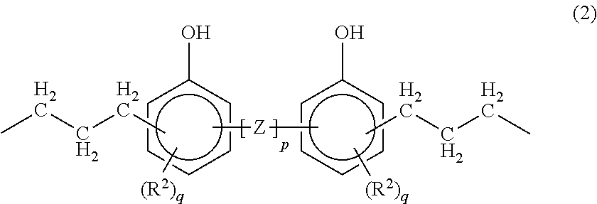
wherein Z is a substituted or unsubstituted divalent hydrocarbon group containing 1 to 15 carbon atoms, and p is 0 or 1, R2 is independently an alkyl group or an alkoxy group containing 1 to 4 carbon atoms, and q is 0, 1, or 2; X2 is independently a divalent group represented by the following formula (3):

wherein R3 is hydrogen atom, monovalent hydrocarbon group containing 1 to 8 carbon atoms, or a glycidyl group; and X3 is independently a divalent group represented by the formula (4):

wherein R4 is independently a monovalent hydrocarbon group containing 1 to 8 carbon atoms, and n an integer of 0 to 100;


wherein R1 is independently a monovalent hydrocarbon group containing 1 to 8 carbon atoms, m is an integer of 0 to 100, e, f, g, h, i and j are an integer of 0 to 100 with the proviso that e+f+g≧3, e and f are not simultaneously 0, and h and i are not simultaneously. X is independently a group represented by the X1, X2, or X3, and the silicon atom at the terminal of the units constituting the repeating unit represented by the formulae (1-1), (1-2), and (1-3) and the units represented by the formulae (5), (6) and (7) is bonded to the terminal carbon atom of the same or different units.

wherein r, s, and t are independently a positive integer; the silicon atom at the terminal of the units constituting the repeating units represented by the formulae (1-1), (1-2), and (1-3) is bonded to the terminal carbon atom of the X1, X2, or X3 in the same or different unit; R1 is independently a monovalent hydrocarbon group containing 1 to 8 carbon atoms; X1 is independently a divalent group represented by the following formula (2):

wherein Z is a substituted or unsubstituted divalent hydrocarbon group containing 1 to 15 carbon atoms, and p is 0 or 1, R2 is independently an alkyl group or an alkoxy group containing 1 to 4 carbon atoms, and q is 0, 1, or 2; X2 is independently a divalent group represented by the following formula (3):

wherein R3 is hydrogen atom, monovalent hydrocarbon group containing 1 to 8 carbon atoms, or a glycidyl group; and X3 is independently a divalent group represented by the formula (4):

wherein R4 is independently a monovalent hydrocarbon group containing 1 to 8 carbon atoms, and n an integer of 0 to 100.

and p is 0 or 1.

wherein R1, R2, R3, R4, Z, n, p, q, r, s, and t are as defined above, and the terminal silicone atom of the units constituting the repeating unit is bonded to the terminal carbon atom of the same or different unit, and the polymer is terminated with an aliphatic unsaturated group or hydrogen atom bonded to the silicon atom.


wherein R1, X, e, f, g, h, i and j are as defined above, and the terminal carbon atom of each unit is bonded to the terminal silicon atom of the units as described above.

wherein R1, R2, R3, R4, Z, n, m, p, q, r, s, t, and b are as defined above, and the terminal silicone atom of the units constituting the repeating unit is bonded to the terminal carbon atom of the same or different unit, and the polymer is terminated with an aliphatic unsaturated group or hydrogen atom bonded to the silicon atom.

wherein R1, R2, R3, R4, Z, n, p, q, e, f, g, r, s, t, and c are as defined above, and the terminal silicone atom of the units constituting the repeating unit is bonded to the terminal carbon atom of the same or different unit, and the polymer is terminated with an aliphatic unsaturated group or hydrogen atom bonded to the silicon atom.

wherein R1, R2, R3, R4, Z, n, p, q, h, i, j, r, s, t, and d are as defined above, and the terminal silicone atom of the units constituting the repeating unit is bonded to the terminal carbon atom of the same or different unit, and the polymer is terminated with an aliphatic unsaturated group or hydrogen atom bonded to the silicon atom.

wherein R1 is as defined above; the compound represented by the following formula (9):

wherein Z, R2, p, and q are as defined above; the compound represented by the following formula (10):

wherein R3 is as defined above; and the compound represented by the following formula (11):

wherein R4 and n are as defined above; in the presence of a metal catalyst.


wherein R1, m, e, f, g, h, i and j are as described above in the presence of a metal catalyst.


-
- EOCN-103S (product name) (epoxy equivalent, 209 to 219; manufactured by Nippon Kayaku Co., Ltd.)
-
- epoxy resin curing agent: RIKACID HH (product name) (hexahydrophthalic anhydride manufactured by New Japan Chemical Co., Ltd.)
- epoxy resin curing aid: Curezol 2P4 MHZ (product name) (2-phenyl-4-methyl-5-hydroxymethylimidazol manufactured by Shikoku Chemical Corporation)
[(C) Filler] - Silica (SE2050; average particle size, 0.50 μm; manufactured by Admatechs)
- Release film (1): E7304 (manufactured by Toyobo Co., Ltd.; 75 μm; peeling strength, 200 mN/50 mm)
- Release film (2): E7302 (manufactured by Toyobo Co., Ltd.; 75 μm; peeling strength, 90 mN/50 mm)
- Protective film: polyethylene film (100 μm)
| TABLE 1 | ||
| Components | Example | Comparative Example |
| (parts by weight) | 1 | 2 | 3 | 4 | 5 | 6 | 7 | 8 | 1 | 2 | 3 |
| Silicone | Synthetic | 100 | 100 | 100 | 100 | 100 | 100 | |||||
| resin (A) | Example 1 | |||||||||||
| Synthetic | 100 | |||||||||||
| Example 2 | ||||||||||||
| Synthetic | 100 | |||||||||||
| Example 3 | ||||||||||||
| Synthetic | 100 | |||||||||||
| Example 4 | ||||||||||||
| Synthetic | 100 | |||||||||||
| Example 5 | ||||||||||||
| Silicone rein | Comparative | 100 | ||||||||||
| outside the | Synthetic | |||||||||||
| scope of the | Example 1 | |||||||||||
| present invention | ||||||||||||
| Thermo- | EOCN-103S | 20 | 20 | 50 | 15 | 20 | 20 | 20 | 20 | 20 | 20 | |
| setting | RIKACID HH | 5 | ||||||||||
| resin (B) | Curezol 2P4MHZ | 1 | 1 | 1 | 1 | 1 | 1 | 1 | 1 | 1 | 1 | |
| Filler (C) | SE2050 | 125 | 400 | 160 | 125 | 125 | 125 | 125 | 125 | 125 | 125 |
| Thickness of the | 200 | 200 | 200 | 200 | 200 | 200 | 200 | 500 | 200 | 200 | 200 |
| resin film (μm) | |||||||||||
| TABLE 2 | |||
| Example | Comparative Example | ||
| Evaluation | 1 | 2 | 3 | 4 | 5 | 6 | 7 | 8 | 1 | 2 | 3 |
| Warpage [mm] | up to 1 | up to 1 | up to 1 | up to 1 | up to 1 | up to 1 | up to 1 | up to 1 | up to 1 | up to 1 | 7 |
| Wafer supporting | Good | Good | Good | Good | Good | Good | Good | Good | Good | Poor | Good |
| ability | |||||||||||
| Adhesion [MPa] | 28.4 | 31.0 | 30.1 | 29.2 | 29.3 | 28.8 | 28.5 | 28.4 | 11.0 | 27.3 | 19.8 |
| Reliability | Good | Good | Good | Good | Good | Good | Good | Good | Poor | Poor | Poor |
Claims (10)


Applications Claiming Priority (2)
| Application Number | Priority Date | Filing Date | Title |
|---|---|---|---|
| JP2011-243359 | 2011-11-07 | ||
| JP2011243359A JP5673496B2 (en) | 2011-11-07 | 2011-11-07 | Resin composition, resin film, semiconductor device and manufacturing method thereof |
Publications (2)
| Publication Number | Publication Date |
|---|---|
| US20130113083A1 US20130113083A1 (en) | 2013-05-09 |
| US8883913B2 true US8883913B2 (en) | 2014-11-11 |
Family
ID=48223139
Family Applications (1)
| Application Number | Title | Priority Date | Filing Date |
|---|---|---|---|
| US13/669,541 Active 2033-02-09 US8883913B2 (en) | 2011-11-07 | 2012-11-06 | Resin composition, resin film, semiconductor device, and production method thereof |
Country Status (2)
| Country | Link |
|---|---|
| US (1) | US8883913B2 (en) |
| JP (1) | JP5673496B2 (en) |
Families Citing this family (7)
| Publication number | Priority date | Publication date | Assignee | Title |
|---|---|---|---|---|
| JP6098531B2 (en) * | 2014-01-23 | 2017-03-22 | 信越化学工業株式会社 | Resin composition, resin film, semiconductor device and manufacturing method thereof |
| JP6265105B2 (en) * | 2014-10-30 | 2018-01-24 | 信越化学工業株式会社 | Silicone resin, resin composition, resin film, semiconductor device and manufacturing method thereof |
| JP6369405B2 (en) * | 2015-07-07 | 2018-08-08 | 信越化学工業株式会社 | Thermosetting resin composition for semiconductor encapsulation |
| JP6683559B2 (en) * | 2016-04-05 | 2020-04-22 | 信越化学工業株式会社 | Resin composition, resin film, resin film manufacturing method, semiconductor device manufacturing method, and semiconductor device |
| US10308787B2 (en) * | 2016-04-05 | 2019-06-04 | Shin-Etsu Chemical Co., Ltd. | Resin composition, resin film, method for producing resin film, method for producing semiconductor device, and semiconductor device |
| JP6466882B2 (en) | 2016-04-27 | 2019-02-06 | 信越化学工業株式会社 | Resin composition, resin film, method for producing resin film, method for producing semiconductor device, and semiconductor device |
| JP6224188B1 (en) | 2016-08-08 | 2017-11-01 | 太陽インキ製造株式会社 | Semiconductor encapsulant |
Citations (12)
| Publication number | Priority date | Publication date | Assignee | Title |
|---|---|---|---|---|
| US3159601A (en) | 1962-07-02 | 1964-12-01 | Gen Electric | Platinum-olefin complex catalyzed addition of hydrogen- and alkenyl-substituted siloxanes |
| US3159662A (en) | 1962-07-02 | 1964-12-01 | Gen Electric | Addition reaction |
| US3220972A (en) | 1962-07-02 | 1965-11-30 | Gen Electric | Organosilicon process using a chloroplatinic acid reaction product as the catalyst |
| US3775452A (en) | 1971-04-28 | 1973-11-27 | Gen Electric | Platinum complexes of unsaturated siloxanes and platinum containing organopolysiloxanes |
| US3882083A (en) * | 1973-11-21 | 1975-05-06 | Gen Electric | Latent addition curable organopolysiloxane compositions |
| US5101029A (en) * | 1989-04-27 | 1992-03-31 | Siemens Aktiengesellschaft | Isocyanurate-containing organosilicon compounds |
| JP2008143954A (en) * | 2006-12-06 | 2008-06-26 | Jsr Corp | Isocyanuric ring-containing polymer, method for producing the same, and composition containing the same |
| JP2008150506A (en) * | 2006-12-18 | 2008-07-03 | Jsr Corp | Curable resin composition and its use |
| WO2009142065A1 (en) | 2008-05-21 | 2009-11-26 | ナガセケムテックス株式会社 | Epoxy resin composition for encapsulating electronic part |
| US20110037174A1 (en) * | 2008-05-16 | 2011-02-17 | Sumitomo Bakelite Co., Ltd. | Method of manufacturing semiconductor component, and semiconductor component |
| US20110262697A1 (en) * | 2008-12-26 | 2011-10-27 | Satoru Katsurayama | Flexible substrate and electronic device |
| US8124715B2 (en) * | 2009-11-04 | 2012-02-28 | Shin-Etsu Chemical Co., Ltd. | Isocyanuric ring-containing polysiloxane having vinyl groups at the terminals |
Family Cites Families (13)
| Publication number | Priority date | Publication date | Assignee | Title |
|---|---|---|---|---|
| US4990546A (en) * | 1990-03-23 | 1991-02-05 | General Electric Company | UV-curable silphenylene-containing epoxy functional silicones |
| JPH09302095A (en) * | 1996-05-10 | 1997-11-25 | Kanegafuchi Chem Ind Co Ltd | Curable composition, molded article and preparation thereof |
| JPH11130865A (en) * | 1997-08-29 | 1999-05-18 | Dow Corning Toray Silicone Co Ltd | Silphenylene compound containing hydroxyphenyl group, silphenylene-modified organic resin |
| JP3829920B2 (en) * | 2001-08-06 | 2006-10-04 | 信越化学工業株式会社 | Organosiloxane polymer compound, photocurable resin composition, pattern forming method, and film for protecting substrate |
| JP3944734B2 (en) * | 2003-01-10 | 2007-07-18 | 信越化学工業株式会社 | Organosiloxane polymer compound, photocurable resin composition, pattern forming method, and film for protecting substrate |
| JP4347103B2 (en) * | 2004-03-22 | 2009-10-21 | 信越化学工業株式会社 | Curable silicone composition |
| WO2006055231A1 (en) * | 2004-11-19 | 2006-05-26 | Dow Corning Corporation | Silicone composition and cured silicone resin |
| JP4336999B2 (en) * | 2007-01-31 | 2009-09-30 | 信越化学工業株式会社 | Silphenylene skeleton-containing polymer compound, photocurable resin composition, pattern forming method, and film for protecting circuit board |
| JP2010265372A (en) * | 2009-05-14 | 2010-11-25 | Shin-Etsu Chemical Co Ltd | Organopolysiloxane with both ends sealed with monomethylallyl isocyanuric rings |
| JP2010265374A (en) * | 2009-05-14 | 2010-11-25 | Shin-Etsu Chemical Co Ltd | Isocyanuric ring-containing polysiloxane with terminal hydrogen |
| JP2010285517A (en) * | 2009-06-10 | 2010-12-24 | Kaneka Corp | Photocurable composition, and insulating thin film and thin film transistor obtained using the same |
| JP5413340B2 (en) * | 2009-09-30 | 2014-02-12 | 信越化学工業株式会社 | Epoxy group-containing polymer compound, photocurable resin composition using the same, pattern forming method, and film for protecting electric / electronic parts |
| JP5547685B2 (en) * | 2011-05-23 | 2014-07-16 | 信越化学工業株式会社 | Adhesive composition, adhesive sheet, semiconductor device protecting material, and semiconductor device |
-
2011
- 2011-11-07 JP JP2011243359A patent/JP5673496B2/en active Active
-
2012
- 2012-11-06 US US13/669,541 patent/US8883913B2/en active Active
Patent Citations (13)
| Publication number | Priority date | Publication date | Assignee | Title |
|---|---|---|---|---|
| US3159601A (en) | 1962-07-02 | 1964-12-01 | Gen Electric | Platinum-olefin complex catalyzed addition of hydrogen- and alkenyl-substituted siloxanes |
| US3159662A (en) | 1962-07-02 | 1964-12-01 | Gen Electric | Addition reaction |
| US3220972A (en) | 1962-07-02 | 1965-11-30 | Gen Electric | Organosilicon process using a chloroplatinic acid reaction product as the catalyst |
| US3775452A (en) | 1971-04-28 | 1973-11-27 | Gen Electric | Platinum complexes of unsaturated siloxanes and platinum containing organopolysiloxanes |
| US3882083A (en) * | 1973-11-21 | 1975-05-06 | Gen Electric | Latent addition curable organopolysiloxane compositions |
| US5101029A (en) * | 1989-04-27 | 1992-03-31 | Siemens Aktiengesellschaft | Isocyanurate-containing organosilicon compounds |
| JP2008143954A (en) * | 2006-12-06 | 2008-06-26 | Jsr Corp | Isocyanuric ring-containing polymer, method for producing the same, and composition containing the same |
| JP2008150506A (en) * | 2006-12-18 | 2008-07-03 | Jsr Corp | Curable resin composition and its use |
| US20110037174A1 (en) * | 2008-05-16 | 2011-02-17 | Sumitomo Bakelite Co., Ltd. | Method of manufacturing semiconductor component, and semiconductor component |
| WO2009142065A1 (en) | 2008-05-21 | 2009-11-26 | ナガセケムテックス株式会社 | Epoxy resin composition for encapsulating electronic part |
| US20110105646A1 (en) | 2008-05-21 | 2011-05-05 | Nagase Chemtex Corporation | Epoxy resin composition for encapsulating electronic part |
| US20110262697A1 (en) * | 2008-12-26 | 2011-10-27 | Satoru Katsurayama | Flexible substrate and electronic device |
| US8124715B2 (en) * | 2009-11-04 | 2012-02-28 | Shin-Etsu Chemical Co., Ltd. | Isocyanuric ring-containing polysiloxane having vinyl groups at the terminals |
Also Published As
| Publication number | Publication date |
|---|---|
| JP2013095915A (en) | 2013-05-20 |
| JP5673496B2 (en) | 2015-02-18 |
| US20130113083A1 (en) | 2013-05-09 |
Similar Documents
| Publication | Publication Date | Title |
|---|---|---|
| US8883913B2 (en) | Resin composition, resin film, semiconductor device, and production method thereof | |
| US9890254B2 (en) | Resin composition, resin film, and semiconductor device and method for manufacturing same | |
| US10026650B2 (en) | Resin composition, resin film, semiconductor device and method of manufacture thereof | |
| US10730273B2 (en) | Resin composition, resin film, semiconductor laminate, method for manufacturing semiconductor laminate, and method for manufacturing semiconductor device | |
| US9447305B2 (en) | Silicone resin, resin composition, resin film, semiconductor device, and making method | |
| US10428239B2 (en) | Resin composition, resin film, method for producing resin film, method for producing semiconductor device, and semiconductor device | |
| TWI728087B (en) | Resin composition, resin film, resin film manufacturing method, semiconductor device manufacturing method, and semiconductor device | |
| JP7222955B2 (en) | Resin composition and resin film | |
| US10308787B2 (en) | Resin composition, resin film, method for producing resin film, method for producing semiconductor device, and semiconductor device | |
| US10035912B2 (en) | Flame retardant resin composition, flame retardant resin film, semiconductor device, and making method | |
| JP5981384B2 (en) | Resin composition, resin film, semiconductor device and manufacturing method thereof | |
| JP6828306B2 (en) | Resin composition, resin film, manufacturing method of semiconductor device and semiconductor device |
Legal Events
| Date | Code | Title | Description |
|---|---|---|---|
| AS | Assignment |
Owner name: SHIN-ETSU CHEMICAL CO., LTD., JAPAN Free format text: ASSIGNMENT OF ASSIGNORS INTEREST;ASSIGNORS:KONDO, KAZUNORI;SUGO, MICHIHIRO;REEL/FRAME:029258/0343 Effective date: 20121012 |
|
| STCF | Information on status: patent grant |
Free format text: PATENTED CASE |
|
| MAFP | Maintenance fee payment |
Free format text: PAYMENT OF MAINTENANCE FEE, 4TH YEAR, LARGE ENTITY (ORIGINAL EVENT CODE: M1551) Year of fee payment: 4 |
|
| MAFP | Maintenance fee payment |
Free format text: PAYMENT OF MAINTENANCE FEE, 8TH YEAR, LARGE ENTITY (ORIGINAL EVENT CODE: M1552); ENTITY STATUS OF PATENT OWNER: LARGE ENTITY Year of fee payment: 8 |