US8871075B2 - Method of forming metal pattern and method of manufacturing display substrate having the same - Google Patents
Method of forming metal pattern and method of manufacturing display substrate having the same Download PDFInfo
- Publication number
- US8871075B2 US8871075B2 US13/405,532 US201213405532A US8871075B2 US 8871075 B2 US8871075 B2 US 8871075B2 US 201213405532 A US201213405532 A US 201213405532A US 8871075 B2 US8871075 B2 US 8871075B2
- Authority
- US
- United States
- Prior art keywords
- metal
- layer
- light
- substrate
- precursor
- Prior art date
- Legal status (The legal status is an assumption and is not a legal conclusion. Google has not performed a legal analysis and makes no representation as to the accuracy of the status listed.)
- Active
Links
Images


Classifications
-
- C—CHEMISTRY; METALLURGY
- C23—COATING METALLIC MATERIAL; COATING MATERIAL WITH METALLIC MATERIAL; CHEMICAL SURFACE TREATMENT; DIFFUSION TREATMENT OF METALLIC MATERIAL; COATING BY VACUUM EVAPORATION, BY SPUTTERING, BY ION IMPLANTATION OR BY CHEMICAL VAPOUR DEPOSITION, IN GENERAL; INHIBITING CORROSION OF METALLIC MATERIAL OR INCRUSTATION IN GENERAL
- C23C—COATING METALLIC MATERIAL; COATING MATERIAL WITH METALLIC MATERIAL; SURFACE TREATMENT OF METALLIC MATERIAL BY DIFFUSION INTO THE SURFACE, BY CHEMICAL CONVERSION OR SUBSTITUTION; COATING BY VACUUM EVAPORATION, BY SPUTTERING, BY ION IMPLANTATION OR BY CHEMICAL VAPOUR DEPOSITION, IN GENERAL
- C23C18/00—Chemical coating by decomposition of either liquid compounds or solutions of the coating forming compounds, without leaving reaction products of surface material in the coating; Contact plating
- C23C18/16—Chemical coating by decomposition of either liquid compounds or solutions of the coating forming compounds, without leaving reaction products of surface material in the coating; Contact plating by reduction or substitution, e.g. electroless plating
- C23C18/18—Pretreatment of the material to be coated
- C23C18/1851—Pretreatment of the material to be coated of surfaces of non-metallic or semiconducting in organic material
- C23C18/1872—Pretreatment of the material to be coated of surfaces of non-metallic or semiconducting in organic material by chemical pretreatment
- C23C18/1875—Pretreatment of the material to be coated of surfaces of non-metallic or semiconducting in organic material by chemical pretreatment only one step pretreatment
- C23C18/1879—Use of metal, e.g. activation, sensitisation with noble metals
-
- C—CHEMISTRY; METALLURGY
- C23—COATING METALLIC MATERIAL; COATING MATERIAL WITH METALLIC MATERIAL; CHEMICAL SURFACE TREATMENT; DIFFUSION TREATMENT OF METALLIC MATERIAL; COATING BY VACUUM EVAPORATION, BY SPUTTERING, BY ION IMPLANTATION OR BY CHEMICAL VAPOUR DEPOSITION, IN GENERAL; INHIBITING CORROSION OF METALLIC MATERIAL OR INCRUSTATION IN GENERAL
- C23C—COATING METALLIC MATERIAL; COATING MATERIAL WITH METALLIC MATERIAL; SURFACE TREATMENT OF METALLIC MATERIAL BY DIFFUSION INTO THE SURFACE, BY CHEMICAL CONVERSION OR SUBSTITUTION; COATING BY VACUUM EVAPORATION, BY SPUTTERING, BY ION IMPLANTATION OR BY CHEMICAL VAPOUR DEPOSITION, IN GENERAL
- C23C18/00—Chemical coating by decomposition of either liquid compounds or solutions of the coating forming compounds, without leaving reaction products of surface material in the coating; Contact plating
- C23C18/16—Chemical coating by decomposition of either liquid compounds or solutions of the coating forming compounds, without leaving reaction products of surface material in the coating; Contact plating by reduction or substitution, e.g. electroless plating
- C23C18/1601—Process or apparatus
- C23C18/1603—Process or apparatus coating on selected surface areas
- C23C18/1607—Process or apparatus coating on selected surface areas by direct patterning
- C23C18/1608—Process or apparatus coating on selected surface areas by direct patterning from pretreatment step, i.e. selective pre-treatment
-
- C—CHEMISTRY; METALLURGY
- C23—COATING METALLIC MATERIAL; COATING MATERIAL WITH METALLIC MATERIAL; CHEMICAL SURFACE TREATMENT; DIFFUSION TREATMENT OF METALLIC MATERIAL; COATING BY VACUUM EVAPORATION, BY SPUTTERING, BY ION IMPLANTATION OR BY CHEMICAL VAPOUR DEPOSITION, IN GENERAL; INHIBITING CORROSION OF METALLIC MATERIAL OR INCRUSTATION IN GENERAL
- C23C—COATING METALLIC MATERIAL; COATING MATERIAL WITH METALLIC MATERIAL; SURFACE TREATMENT OF METALLIC MATERIAL BY DIFFUSION INTO THE SURFACE, BY CHEMICAL CONVERSION OR SUBSTITUTION; COATING BY VACUUM EVAPORATION, BY SPUTTERING, BY ION IMPLANTATION OR BY CHEMICAL VAPOUR DEPOSITION, IN GENERAL
- C23C18/00—Chemical coating by decomposition of either liquid compounds or solutions of the coating forming compounds, without leaving reaction products of surface material in the coating; Contact plating
- C23C18/16—Chemical coating by decomposition of either liquid compounds or solutions of the coating forming compounds, without leaving reaction products of surface material in the coating; Contact plating by reduction or substitution, e.g. electroless plating
- C23C18/1601—Process or apparatus
- C23C18/1603—Process or apparatus coating on selected surface areas
- C23C18/1607—Process or apparatus coating on selected surface areas by direct patterning
- C23C18/1612—Process or apparatus coating on selected surface areas by direct patterning through irradiation means
-
- C—CHEMISTRY; METALLURGY
- C23—COATING METALLIC MATERIAL; COATING MATERIAL WITH METALLIC MATERIAL; CHEMICAL SURFACE TREATMENT; DIFFUSION TREATMENT OF METALLIC MATERIAL; COATING BY VACUUM EVAPORATION, BY SPUTTERING, BY ION IMPLANTATION OR BY CHEMICAL VAPOUR DEPOSITION, IN GENERAL; INHIBITING CORROSION OF METALLIC MATERIAL OR INCRUSTATION IN GENERAL
- C23C—COATING METALLIC MATERIAL; COATING MATERIAL WITH METALLIC MATERIAL; SURFACE TREATMENT OF METALLIC MATERIAL BY DIFFUSION INTO THE SURFACE, BY CHEMICAL CONVERSION OR SUBSTITUTION; COATING BY VACUUM EVAPORATION, BY SPUTTERING, BY ION IMPLANTATION OR BY CHEMICAL VAPOUR DEPOSITION, IN GENERAL
- C23C18/00—Chemical coating by decomposition of either liquid compounds or solutions of the coating forming compounds, without leaving reaction products of surface material in the coating; Contact plating
- C23C18/16—Chemical coating by decomposition of either liquid compounds or solutions of the coating forming compounds, without leaving reaction products of surface material in the coating; Contact plating by reduction or substitution, e.g. electroless plating
- C23C18/1601—Process or apparatus
- C23C18/1633—Process of electroless plating
- C23C18/1646—Characteristics of the product obtained
- C23C18/165—Multilayered product
- C23C18/1653—Two or more layers with at least one layer obtained by electroless plating and one layer obtained by electroplating
-
- C—CHEMISTRY; METALLURGY
- C23—COATING METALLIC MATERIAL; COATING MATERIAL WITH METALLIC MATERIAL; CHEMICAL SURFACE TREATMENT; DIFFUSION TREATMENT OF METALLIC MATERIAL; COATING BY VACUUM EVAPORATION, BY SPUTTERING, BY ION IMPLANTATION OR BY CHEMICAL VAPOUR DEPOSITION, IN GENERAL; INHIBITING CORROSION OF METALLIC MATERIAL OR INCRUSTATION IN GENERAL
- C23C—COATING METALLIC MATERIAL; COATING MATERIAL WITH METALLIC MATERIAL; SURFACE TREATMENT OF METALLIC MATERIAL BY DIFFUSION INTO THE SURFACE, BY CHEMICAL CONVERSION OR SUBSTITUTION; COATING BY VACUUM EVAPORATION, BY SPUTTERING, BY ION IMPLANTATION OR BY CHEMICAL VAPOUR DEPOSITION, IN GENERAL
- C23C18/00—Chemical coating by decomposition of either liquid compounds or solutions of the coating forming compounds, without leaving reaction products of surface material in the coating; Contact plating
- C23C18/16—Chemical coating by decomposition of either liquid compounds or solutions of the coating forming compounds, without leaving reaction products of surface material in the coating; Contact plating by reduction or substitution, e.g. electroless plating
- C23C18/18—Pretreatment of the material to be coated
- C23C18/1851—Pretreatment of the material to be coated of surfaces of non-metallic or semiconducting in organic material
- C23C18/1862—Pretreatment of the material to be coated of surfaces of non-metallic or semiconducting in organic material by radiant energy
- C23C18/1865—Heat
-
- C—CHEMISTRY; METALLURGY
- C23—COATING METALLIC MATERIAL; COATING MATERIAL WITH METALLIC MATERIAL; CHEMICAL SURFACE TREATMENT; DIFFUSION TREATMENT OF METALLIC MATERIAL; COATING BY VACUUM EVAPORATION, BY SPUTTERING, BY ION IMPLANTATION OR BY CHEMICAL VAPOUR DEPOSITION, IN GENERAL; INHIBITING CORROSION OF METALLIC MATERIAL OR INCRUSTATION IN GENERAL
- C23C—COATING METALLIC MATERIAL; COATING MATERIAL WITH METALLIC MATERIAL; SURFACE TREATMENT OF METALLIC MATERIAL BY DIFFUSION INTO THE SURFACE, BY CHEMICAL CONVERSION OR SUBSTITUTION; COATING BY VACUUM EVAPORATION, BY SPUTTERING, BY ION IMPLANTATION OR BY CHEMICAL VAPOUR DEPOSITION, IN GENERAL
- C23C18/00—Chemical coating by decomposition of either liquid compounds or solutions of the coating forming compounds, without leaving reaction products of surface material in the coating; Contact plating
- C23C18/16—Chemical coating by decomposition of either liquid compounds or solutions of the coating forming compounds, without leaving reaction products of surface material in the coating; Contact plating by reduction or substitution, e.g. electroless plating
- C23C18/18—Pretreatment of the material to be coated
- C23C18/1851—Pretreatment of the material to be coated of surfaces of non-metallic or semiconducting in organic material
- C23C18/1862—Pretreatment of the material to be coated of surfaces of non-metallic or semiconducting in organic material by radiant energy
- C23C18/1868—Radiation, e.g. UV, laser
-
- C—CHEMISTRY; METALLURGY
- C23—COATING METALLIC MATERIAL; COATING MATERIAL WITH METALLIC MATERIAL; CHEMICAL SURFACE TREATMENT; DIFFUSION TREATMENT OF METALLIC MATERIAL; COATING BY VACUUM EVAPORATION, BY SPUTTERING, BY ION IMPLANTATION OR BY CHEMICAL VAPOUR DEPOSITION, IN GENERAL; INHIBITING CORROSION OF METALLIC MATERIAL OR INCRUSTATION IN GENERAL
- C23C—COATING METALLIC MATERIAL; COATING MATERIAL WITH METALLIC MATERIAL; SURFACE TREATMENT OF METALLIC MATERIAL BY DIFFUSION INTO THE SURFACE, BY CHEMICAL CONVERSION OR SUBSTITUTION; COATING BY VACUUM EVAPORATION, BY SPUTTERING, BY ION IMPLANTATION OR BY CHEMICAL VAPOUR DEPOSITION, IN GENERAL
- C23C18/00—Chemical coating by decomposition of either liquid compounds or solutions of the coating forming compounds, without leaving reaction products of surface material in the coating; Contact plating
- C23C18/54—Contact plating, i.e. electroless electrochemical plating
-
- G—PHYSICS
- G02—OPTICS
- G02F—OPTICAL DEVICES OR ARRANGEMENTS FOR THE CONTROL OF LIGHT BY MODIFICATION OF THE OPTICAL PROPERTIES OF THE MEDIA OF THE ELEMENTS INVOLVED THEREIN; NON-LINEAR OPTICS; FREQUENCY-CHANGING OF LIGHT; OPTICAL LOGIC ELEMENTS; OPTICAL ANALOGUE/DIGITAL CONVERTERS
- G02F1/00—Devices or arrangements for the control of the intensity, colour, phase, polarisation or direction of light arriving from an independent light source, e.g. switching, gating or modulating; Non-linear optics
- G02F1/01—Devices or arrangements for the control of the intensity, colour, phase, polarisation or direction of light arriving from an independent light source, e.g. switching, gating or modulating; Non-linear optics for the control of the intensity, phase, polarisation or colour
- G02F1/13—Devices or arrangements for the control of the intensity, colour, phase, polarisation or direction of light arriving from an independent light source, e.g. switching, gating or modulating; Non-linear optics for the control of the intensity, phase, polarisation or colour based on liquid crystals, e.g. single liquid crystal display cells
- G02F1/133—Constructional arrangements; Operation of liquid crystal cells; Circuit arrangements
- G02F1/1333—Constructional arrangements; Manufacturing methods
Definitions
- Exemplary embodiments of the invention relate generally to flat panel displays. More particularly, exemplary embodiments of the invention relate to a method of forming a metal pattern and a method of manufacturing a display substrate having the metal pattern.
- a liquid crystal display (“LCD”) panel includes a display substrate, a counter substrate facing the display substrate and a liquid crystal layer interposed between the display substrate and the counter substrate.
- the display substrate includes a gate line formed on a base substrate and applied with a gate signal, a data line crossing the gate line, a thin-film transistor (“TFT”) electrically connected to the gate and data lines, and a pixel electrode electrically connected to the TFT.
- TFT thin-film transistor
- the gate and data lines become longer so that a signal delay is occurred.
- the gate line and/or the data line have relatively large thickness, or when a signal line includes a metal having a low resistance, the signal delay could be improved.
- a metal having a low resistance is limitative, and it is difficult to control processes of manufacturing the display substrate such that inherent property of the metal, such as aluminum, copper, is not changed.
- general processes of forming a signal line need a plurality of masks for patterning, a high vacuum deposition process, and several processes such as etching and washing. Therefore, performing the above processes costs high, and noxious substances may be discharged.
- the precision of the signal line is deteriorated and it is hard to form a fine pattern.
- Exemplary embodiments of the invention provide a method of forming a metal pattern to form relatively thick signal line in a simple process.
- Exemplary embodiments of the invention also provide a method of manufacturing a display substrate including the method of forming a metal pattern.
- a method of forming a metal pattern includes forming a precursor layer including a metal precursor on a substrate, irradiating a light on the precursor layer to form a metal seed layer having a predetermined pattern, and electroless-plating the metal seed layer to form a metal pattern layer.
- a method of manufacturing a display substrate includes forming a gate pattern including gate lines and a gate electrode, forming a source pattern on the substrate including the gate pattern, and forming a pixel electrode on the substrate including the source pattern.
- the forming a gate pattern includes forming a precursor layer including a metal precursor on a substrate, irradiating a light on the precursor layer to form a metal seed layer having a predetermined pattern, and electroless-plating the metal seed layer to form a metal pattern layer.
- the source pattern includes date lines, a source electrode and a drain electrode.
- the pixel electrode is in electrical connection to the drain electrode.
- the exposure process and the annealing process are sequentially performed in the one process of irradiating the light from single light source onto the substrate, so that total processes of forming a metal pattern on the substrate are simplified.
- an electroless-plating is performed after forming the metal seed layer, so that a metal pattern having a uniform distribution can be formed on the substrate having large area.
- the electro-plating is performed after the electroless-plating so that the thickness of the metal pattern layer is increase efficiently.
- the metal pattern may be formed to have high ratio of width to thickness, so that a signal line having small electric resistance and fast response may be formed.
- FIG. 1 is a flowchart explaining an exemplary embodiment of a method of forming a metal pattern according to the invention
- FIGS. 2A to 2C are cross-sectional view explaining an exemplary embodiment of the process of forming a precursor layer in FIG. 1 ;
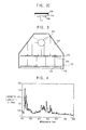
- FIG. 3 is a conceptual diagram explaining an exemplary embodiment of the process of forming a metal seed layer in FIG. 1 ;
- FIG. 4 is a graph illustrating wavelength and intensity of a Xenon (Xe) lamp
- FIG. 5 is a plan view illustrating an exemplary embodiment of a substrate after the process of forming a metal seed layer in FIG. 1 ;
- FIG. 6 is a conceptual diagram explaining an exemplary embodiment of the process of electroless-plating in a process of forming a metal pattern layer in FIG. 1 ;
- FIG. 7 is a perspective view illustrating an exemplary embodiment of a substrate after the process of forming a metal pattern layer in FIG. 1 ;
- FIG. 8 is a conceptual diagram explaining another exemplary embodiment of the process of forming a precursor layer according to the invention.
- FIG. 9 is a conceptual diagram explaining another exemplary embodiment of the process of forming a metal seed layer according to the invention.
- FIG. 10 is a conceptual diagram explaining still another exemplary embodiment of the process of forming a metal seed layer according to the invention.
- FIG. 11 is a flowchart explaining another exemplary embodiment of a method of forming a metal pattern according to the invention.
- FIG. 12 is a conceptual diagram explaining an exemplary embodiment of the process of electro-plating a metal pattern layer in FIG. 11 ;
- FIG. 13 is a plan view illustrating an exemplary embodiment of a display substrate manufactured by a method of manufacturing a display substrate according to the invention.
- FIG. 14 is a cross-sectional view cut along line I-I′ in FIG. 13 ;
- FIGS. 15A to 15C are cross-sectional views illustrating an exemplary embodiment of a method of manufacturing the display substrate in FIG. 13 .
- first, second, third, etc. may be used herein to describe various elements, components, regions, layers and/or sections, these elements, components, regions, layers and/or sections should not be limited by these terms. These terms are only used to distinguish one element, component, region, layer or section from another region, layer or section. Thus, a first element, component, region, layer or section discussed below could be termed a second element, component, region, layer or section without departing from the teachings of the invention.
- spatially relative terms such as “under,” “above,” and the like, may be used herein for ease of description to describe the relationship of one element or feature to another element(s) or feature(s) as illustrated in the figures. It will be understood that the spatially relative terms are intended to encompass different orientations of the device in use or operation, in addition to the orientation depicted in the figures. For example, if the device in the figures is turned over, elements described as “under” relative to other elements or features would then be oriented “above” relative to the other elements or features. Thus, the exemplary term “under” can encompass both an orientation of above and below. The device may be otherwise oriented (rotated 90 degrees or at other orientations) and the spatially relative descriptors used herein interpreted accordingly.
- FIG. 1 is a flowchart explaining an exemplary embodiment of a method of forming a metal pattern according to the invention.
- a method (step S 100 ) of forming a metal pattern includes forming a precursor layer on a substrate (step S 110 ), irradiating a light on the precursor layer to form a metal seed layer (step S 120 ) and electroless-plating (e.g., via electrolysis) the metal seed layer to form a metal pattern layer (step S 130 ).
- steps S 110 , S 120 and S 130 will be explained in further detail referring to FIGS. 2A to 7 .
- FIGS. 2A to 2C are cross-sectional views explaining the process of forming a precursor layer in FIG. 1 .
- forming a precursor layer includes applying a metal precursor solution 102 on a substrate 110 , rotating the substrate 110 to spread the metal precursor solution 102 on the substrate 110 and drying the substrate 110 .
- the substrate 110 is fixed on a spin plate 200 , and then the metal precursor solution 102 is applied on the substrate 110 .
- the metal precursor includes copper (Cu).
- the metal precursor may include silver (Ag), titanium (Ti), gold (Au), palladium (Pd), etc.
- various metal precursors may be used as desired.
- the spin plate 200 on which the substrate 110 is fixed may be rotated.
- the substrate 110 is rotated with the spin plate 200 , thus the metal precursor solution 102 is spread on the substrate 110 to be uniformly distributed on the substrate 110 .
- the substrate 110 including the spread metal precursor solution 102 is subjected to a drying operation to form a precursor layer 120 on the substrate 110 . Accordingly, the precursor layer 120 is uniformly distributed on the substrate 110 .
- FIG. 3 is a conceptual diagram explaining an exemplary embodiment of the process of forming a metal seed layer in FIG. 1 .
- FIG. 4 is a graph illustrating wavelength in units of nanometer (nm) and intensity in units of ( ⁇ W/cm 2 ), of a Xenon (Xe) lamp.
- forming a metal seed layer includes irradiating a light on the precursor layer 120 with a predetermined pattern to expose the precursor layer 120 , and annealing the exposed precursor layer 120 by the light.
- the substrate 110 on which the precursor layer 120 is formed is disposed in an exposure device 500 , and then light is irradiated from a light source 400 .
- a mask 300 having a predetermined pattern 310 is disposed above the substrate 110 so that the light from the light source 400 passes through the pattern 310 of the mask 300 .
- the precursor layer 120 is exposed to the light having passed through the pattern 310 of the mask 300 .
- the light source 400 has a wavelength having a wide bandwidth.
- the wavelength of the light source 400 has a bandwidth between about 180 nm and about 1000 nm.
- the light source 400 has certain level of intensity respectively in the wavelength between about 180 nm and about 400 nm, and in the wavelength between about 400 nm and about 1000 nm.
- the light source 400 may include a Xenon (Xe) lamp.
- the Xenon lamp has certain level of intensity respectively in the wavelength between about 200 nm and about 300 nm, and in the wavelength between about 400 nm and about 600 nm.
- the light source 400 may be controlled by a control device to have a wavelength having a wide bandwidth.
- the light source 400 may be controlled to have certain level of intensity respectively in the wavelength between about 180 nm and about 400 nm, and in the wavelength between about 400 nm and about 1000 nm using the control device, and the controlled light source may be used in an exposure process.
- the metal precursor in the precursor layer 120 is reduced in the wavelength between about 180 nm and about 400 nm.
- the metal precursor including a copper precursor is irradiated by the light having the wavelength between about 180 nm and about 400 nm, copper ions of the copper precursor (Cu2+) is reduced into copper (Cu). Therefore, the copper is reduced on the substrate 110 by the light.
- the reduced copper is annealed by the light having the wavelength between about 400 nm and about 1000 nm.
- the reduced copper is stabilized by the annealing process.
- the light source 400 has a wavelength having a wide bandwidth between about 180 nm and about 1000 nm, so that the light source 400 may be used both in the exposure process and in the annealing process.
- the metal precursor when the light from the light source 400 is irradiated onto the substrate 100 , the metal precursor is reduced in the wavelength between about 180 nm and about 400 nm of the light, and then the reduced metal is annealed in the wavelength between about 400 nm and about 1000 nm of the light.
- an area 122 where the precursor layer 120 is irradiated by light with a predetermined pattern, is reduced and is sequentially annealed by the light. After the reducing and annealing processes, the area 122 of the precursory layer 120 becomes a metal seed layer 122 formed on the substrate 110 with a predetermined pattern.
- the substrate 110 is washed by a washing process. Through the washing process, the precursor layer 120 is removed except for the metal seed layer 122 , so that only the metal seed layer 122 remains on the substrate 110 .
- the exposure process and the annealing process are sequentially performed in the one process of irradiating the light from the light source 400 onto the substrate 110 , so that total processes of forming a metal pattern on the substrate is simplified. Moreover, the washing process may be also simplified.
- FIG. 5 is a plan view illustrating an exemplary embodiment of a substrate after the process of forming a metal seed layer in FIG. 1 .
- the metal seed layer 122 which has a predetermined pattern remains on the substrate 110 after the washing process.
- the metal seed layer 122 is used as a plating seed in an electroless-plating process.
- the metal seed layer 122 includes a plurality of metal seeds having a dot shape.
- the metal seed layer 122 may include any of a number of shapes of discrete, individual elements.
- FIG. 6 is a conceptual diagram explaining an exemplary embodiment of the process of electroless-plating in a process of forming a metal pattern layer in FIG. 1 .
- FIG. 7 is a perspective view illustrating an exemplary embodiment of a substrate after a process of forming a metal pattern layer in FIG. 1 .
- the substrate 110 where the metal seed layer 122 is formed, is electroless-plated to form a metal pattern layer on the substrate 110 (step S 130 ).
- plating solution 610 including a soluble oxidizer is filled in an electroless-plating device 600 , and the soluble oxidizer includes a second metal 612 . Thereafter, the substrate 110 is exposed to the plating solution 610 .
- the metal seed layer 122 includes a first metal which has a reducing power smaller than that of the second metal.
- the first metal includes copper (Cu)
- the metal seed layer 122 is used as a plating seed, so that the second metal is continuously reduced. Therefore, a metal pattern layer 124 having a predetermined line shape is formed. In the process, groups of the discrete, individual elements of the metal seed layer 122 collectively form a sub-pattern of the metal pattern layer 124 .
- a metal pattern layer 124 having a predetermined line pattern is formed on the substrate 110 .
- the metal pattern layer 124 includes a plurality of line patterns, each being a single, unitary, indivisible member which is formed from a group of the discrete, individual elements of the metal seed layer 122 .
- an electroless-plating is performed after a metal seed layer is formed on a substrate, so that a metal pattern having a uniform distribution can be formed on the substrate having a large area. Therefore, a fine metal pattern can be formed more uniformly and precisely. Moreover, a fine metal pattern having a width smaller than 0.1 micrometer ( ⁇ m) can be formed according to the resolution of the mask 300 .
- the metal seed layer includes copper, cost for a metal patterning process can be reduced.
- FIG. 8 is a conceptual diagram explaining another exemplary embodiment of the process of forming a precursor layer according to the invention.
- a method of forming a metal pattern according to the illustrated exemplary embodiment is substantially the same as the method of forming a metal pattern according to the exemplary embodiment shown in FIG. 1 except for the process of forming a precursor layer.
- the same reference numbers will be used throughout the drawings to refer to the same or like parts, and any repetitive explanation will be omitted.
- a metal precursor 102 is uniformly distributed on the substrate 110 using a uniform droplet diffuser 800 to form the precursor layer 120 .
- the uniform droplet diffuser 800 moves evenly above the substrate 110 , so that the precursor layer 120 is formed uniformly on the substrate 110 .
- the uniform droplet diffuser 800 uniformly diffuses droplet on the substrate.
- the uniform droplet diffuser 800 may include a spray, an electrospray, etc.
- any uniform droplet diffuser that can uniformly diffuse droplet may be used instead of the spray and the electrospray.
- FIG. 9 is a conceptual diagram explaining another exemplary embodiment of the process of forming a metal seed layer according to the invention.
- a method of forming a metal pattern according to the illustrated exemplary embodiment is substantially the same as the method of forming a metal pattern according to the exemplary embodiment shown in FIG. 1 except for the process of forming a metal seed layer.
- the same reference numbers will be used throughout the drawings to refer to the same or like parts, and any repetitive explanation will be omitted.
- the light from the light source 400 is condensed by a condenser 410 without a mask, and the precursor layer 120 is irradiated by the condensed light.
- the condenser 410 is disposed on the light source 400 , and the light condensed by the condenser 410 is directly irradiated on the substrate 110 with a predetermined pattern using moving device, such as moving stage (not shown). Accordingly, a metal seed layer 124 can be selectively formed on the substrate 110 from the precursor layer 120 , with a predetermined pattern. Therefore, a mask can be omitted in the process of irradiating a light on the precursor layer 120 , and total processes of forming a metal pattern layer can be substituted for an in-line process.
- FIG. 10 is a conceptual diagram explaining still another exemplary embodiment of the process of forming a metal seed layer according to the invention.
- a method of forming a metal pattern according to the illustrated exemplary embodiment is substantially the same as the method of forming a metal pattern according to the exemplary embodiment shown in FIG. 1 except for the process of forming a metal seed layer.
- the same reference numbers will be used throughout the drawings to refer to the same or like parts, and any repetitive explanation will be omitted.
- a condensing lens 900 is disposed under the mask 300 which is disposed in the exposure device 500 .
- the light having passed through the mask 300 is condensed and refined by the condensing lens 900 .
- the condensed and refined light is irradiated on the precursor layer 120 , so that the metal seed layer 122 formed through the exposure and annealing processes may be uniform and stable. Moreover, a damage of the mask 300 can be minimized and a resolution of pattern can be improved.
- a single condensing lens is used. However, a plurality of condensing lenses may be disposed under the mask 300 corresponding to the pattern of the mask 300 , or the substrate 110 may move in various patterns on a moving stage (not illustrated).
- FIG. 11 is a flowchart explaining another exemplary embodiment of a method of forming a metal pattern according to the invention.
- FIG. 12 is a conceptual diagram explaining an exemplary embodiment of a process of electro-plating a metal pattern layer in FIG. 11 .
- a method (step S 101 ) of forming a metal pattern according to the illustrated exemplary embodiment is substantially the same as the method of forming a metal pattern according to the exemplary embodiment shown in FIG. 1 except that the substrate, where the metal pattern layer is formed, is electro-plated additionally.
- the same reference numbers will be used throughout the drawings to refer to the same or like parts, and any repetitive explanation will be omitted.
- the substrate, where the metal pattern layer 124 is formed is electro-plated (step S 140 ).
- the substrate 110 including the formed metal pattern layer 124 is disposed in an electro-plating device 700 , and the metal pattern layer 124 is electrically connected to a cathode of the electro-plating device 700 .
- a plating solution 710 is filled in the electro-plating device 700 and a voltage is applied to the cathode and an anode of the electro-plating device 700 , and then the substrate 110 is charged to be a cathode and the plating solution 710 is charged to be an anode.
- a metal ion of the plating solution 710 is reduced on the metal pattern layer 124 by electrolysis, so that thickness of the metal pattern layer 124 increases.
- the metal included in the plating solution 710 is chosen to be same as the second metal included in the metal pattern layer 124 , so that the thickness of the metal pattern layer 124 may increase.
- the electro-plating is performed after the electroless-plating so that the thickness of the metal pattern layer 124 increases efficiently.
- a metal layer may be formed quickly, but thickness distribution of the metal layer on large area may not be uniform.
- the electroless-plating is performed before the electro-plating, so that the speed of forming the metal pattern of the metal pattern layer is relatively slow, but the metal pattern is uniformly formed.
- the electro-plating is performed so that the thickness of the metal pattern of the metal pattern layer formed by the electroless-plating process may increase quickly. Therefore, the final metal pattern layer may be totally uniformly formed and may have high ratio of width to thickness.
- the metal pattern layer has high ratio of width to thickness, so that a signal line having small electric resistance and fast response may be formed.
- FIG. 13 is a plan view illustrating an exemplary embodiment of a display substrate manufactured by a method of manufacturing a display substrate according to the invention.
- FIG. 14 is a cross-sectional view cut along line I-I′ in FIG. 13 .
- a display substrate 10 includes first and second gate lines GL 1 and GL 2 on an insulting substrate 110 , first and second data lines DL 1 and DL 2 , and a switching element having a thin film transistor SW and a pixel electrode PE.
- the display substrate 10 may further include a gate insulting layer 130 and a passivation layer 150 .
- An exemplary embodiment of a method of manufacturing the display substrate 10 will be explained in further detail referring to FIGS. 15A to 15C .
- FIGS. 15A to 15C are cross-sectional views illustrating an exemplary embodiment of a method of manufacturing the display substrate 10 in FIG. 13 .
- a gate pattern 124 including the first and second gate lines GL 1 and GL 2 and a gate electrode GE is formed on the insulting substrate 110 .
- a method of forming the gate pattern 124 according to the illustrated exemplary embodiment is substantially the same as the method of forming a metal pattern according to the exemplary embodiment shown in FIGS. 1 to 7 . Thus, any repetitive explanation will be omitted.
- the gate insulating layer 130 is formed on the insulting substrate 110 where the gate pattern 124 is formed. Thereafter, a semiconductor pattern AP including a semiconductor layer 142 and an ohmic contact layer 144 is formed on the gate insulting layer 130 , and a source pattern including the first and second data lines DL 1 and DL 2 , a source electrode SE and a drain electrode DE is formed.
- the passivation layer 150 is formed on the insulating substrate 110 where the source pattern is formed, and then a contact hole CNT is formed in the passivation layer 150 .
- the pixel electrode PE is formed on the passivation layer 150 including the contact hole CNT, so that the display substrate 10 shown in FIG. 13 is manufactured.
- the exposure process and the annealing process are sequentially performed in the one process of irradiating the light from single light source onto the substrate, so that total processes of forming a metal pattern on the substrate are simplified.
- an electroless-plating is performed after forming the metal seed layer, so that a metal pattern having a uniform distribution can be formed on the substrate having large area.
- the electro-plating is performed after the electroless-plating so that the thickness of the metal pattern layer is increase efficiently.
- the metal pattern may be formed to have high ratio of width to thickness, so that a signal line having small electric resistance and fast response may be formed.
Abstract
Description
Cu+2[Ag(NH3)2]NO3=[Cu(NH3)4](NO3)2+2Ag [Equation 1]
Claims (18)
Applications Claiming Priority (3)
| Application Number | Priority Date | Filing Date | Title |
|---|---|---|---|
| KR2011-0020891 | 2011-03-09 | ||
| KR1020110020891A KR101765731B1 (en) | 2011-03-09 | 2011-03-09 | Method of forming metal pattern and method of manufacturing display substrate having the same |
| KR10-2011-0020891 | 2011-03-09 |
Publications (2)
| Publication Number | Publication Date |
|---|---|
| US20120231567A1 US20120231567A1 (en) | 2012-09-13 |
| US8871075B2 true US8871075B2 (en) | 2014-10-28 |
Family
ID=46795937
Family Applications (1)
| Application Number | Title | Priority Date | Filing Date |
|---|---|---|---|
| US13/405,532 Active US8871075B2 (en) | 2011-03-09 | 2012-02-27 | Method of forming metal pattern and method of manufacturing display substrate having the same |
Country Status (2)
| Country | Link |
|---|---|
| US (1) | US8871075B2 (en) |
| KR (1) | KR101765731B1 (en) |
Citations (14)
| Publication number | Priority date | Publication date | Assignee | Title |
|---|---|---|---|---|
| US5098526A (en) * | 1991-04-08 | 1992-03-24 | The United States Of America As Represented By The United States Department Of Energy | Process for preparation of a seed layer for selective metal deposition |
| US5264108A (en) * | 1992-09-08 | 1993-11-23 | The United States Of America As Represented By The United States Department Of Energy | Laser patterning of laminated structures for electroplating |
| US5336630A (en) * | 1991-11-15 | 1994-08-09 | Goldstar Electron Co., Ltd. | Method of making semiconductor memory device |
| US5559583A (en) * | 1994-02-24 | 1996-09-24 | Nec Corporation | Exposure system and illuminating apparatus used therein and method for exposing a resist film on a wafer |
| US6121076A (en) * | 1993-05-26 | 2000-09-19 | Semiconductor Energy Laboratory Co., Ltd. | Method for producing semiconductor device |
| US6468839B2 (en) * | 1993-11-05 | 2002-10-22 | Sony Corporation | Thin film semiconductor device for display and method of producing same |
| US6806189B2 (en) * | 2002-03-07 | 2004-10-19 | Lg.Philips Lcd Co., Ltd. | Method of silver (AG) electroless plating on ITO electrode |
| US20070134902A1 (en) * | 2005-12-12 | 2007-06-14 | The Curators Of The University Of Missouri | Patterning of Substrates with Metal-Containing Particles |
| US20080135980A1 (en) * | 2003-10-09 | 2008-06-12 | Matsushita Electric Industrial Co., Ltd. | Method for making junction and processed material formed using the same |
| US7438950B2 (en) * | 2004-06-01 | 2008-10-21 | Fujifilm Corporation | Metallic pattern forming method and conductive pattern material |
| US7446166B2 (en) * | 2005-04-13 | 2008-11-04 | Industry - University Cooperation Foundation Sogang University | Pyrrole derivative and photosensitive film using the same |
| US20090249976A1 (en) * | 2003-07-11 | 2009-10-08 | Tom Etheridge | Palladium complexes for printing circuits |
| US7659138B2 (en) * | 2003-12-26 | 2010-02-09 | Semiconductor Energy Laboratory Co., Ltd. | Method for manufacturing an organic semiconductor element |
| US20100311238A1 (en) * | 2005-02-04 | 2010-12-09 | Hiroki Nakamura | Method of forming copper wiring layer |
Family Cites Families (1)
| Publication number | Priority date | Publication date | Assignee | Title |
|---|---|---|---|---|
| JP2009004669A (en) * | 2007-06-25 | 2009-01-08 | Panasonic Corp | Method for manufacturing metal wiring substrate and metal wiring substrate formed by using it |
-
2011
- 2011-03-09 KR KR1020110020891A patent/KR101765731B1/en active IP Right Grant
-
2012
- 2012-02-27 US US13/405,532 patent/US8871075B2/en active Active
Patent Citations (14)
| Publication number | Priority date | Publication date | Assignee | Title |
|---|---|---|---|---|
| US5098526A (en) * | 1991-04-08 | 1992-03-24 | The United States Of America As Represented By The United States Department Of Energy | Process for preparation of a seed layer for selective metal deposition |
| US5336630A (en) * | 1991-11-15 | 1994-08-09 | Goldstar Electron Co., Ltd. | Method of making semiconductor memory device |
| US5264108A (en) * | 1992-09-08 | 1993-11-23 | The United States Of America As Represented By The United States Department Of Energy | Laser patterning of laminated structures for electroplating |
| US6121076A (en) * | 1993-05-26 | 2000-09-19 | Semiconductor Energy Laboratory Co., Ltd. | Method for producing semiconductor device |
| US6468839B2 (en) * | 1993-11-05 | 2002-10-22 | Sony Corporation | Thin film semiconductor device for display and method of producing same |
| US5559583A (en) * | 1994-02-24 | 1996-09-24 | Nec Corporation | Exposure system and illuminating apparatus used therein and method for exposing a resist film on a wafer |
| US6806189B2 (en) * | 2002-03-07 | 2004-10-19 | Lg.Philips Lcd Co., Ltd. | Method of silver (AG) electroless plating on ITO electrode |
| US20090249976A1 (en) * | 2003-07-11 | 2009-10-08 | Tom Etheridge | Palladium complexes for printing circuits |
| US20080135980A1 (en) * | 2003-10-09 | 2008-06-12 | Matsushita Electric Industrial Co., Ltd. | Method for making junction and processed material formed using the same |
| US7659138B2 (en) * | 2003-12-26 | 2010-02-09 | Semiconductor Energy Laboratory Co., Ltd. | Method for manufacturing an organic semiconductor element |
| US7438950B2 (en) * | 2004-06-01 | 2008-10-21 | Fujifilm Corporation | Metallic pattern forming method and conductive pattern material |
| US20100311238A1 (en) * | 2005-02-04 | 2010-12-09 | Hiroki Nakamura | Method of forming copper wiring layer |
| US7446166B2 (en) * | 2005-04-13 | 2008-11-04 | Industry - University Cooperation Foundation Sogang University | Pyrrole derivative and photosensitive film using the same |
| US20070134902A1 (en) * | 2005-12-12 | 2007-06-14 | The Curators Of The University Of Missouri | Patterning of Substrates with Metal-Containing Particles |
Also Published As
| Publication number | Publication date |
|---|---|
| US20120231567A1 (en) | 2012-09-13 |
| KR101765731B1 (en) | 2017-08-08 |
| KR20120102954A (en) | 2012-09-19 |
Similar Documents
| Publication | Publication Date | Title |
|---|---|---|
| KR100841170B1 (en) | Method of preparing low resistance metal line, patterned metal line structure, and display devices using the same | |
| US8127674B2 (en) | Stamp and fabricating method thereof, thin film transistor using the stamp, and liquid crystal display device having the thin film transistor | |
| CN102116984B (en) | Liquid crystal display device and method for fabricating the same | |
| US20070236641A1 (en) | Thin film transistor substrate and method of fabricating the same | |
| US7315344B2 (en) | Liquid crystal display device and method of fabricating the same | |
| KR100847985B1 (en) | Method of preparing metal line | |
| US8426229B2 (en) | Method of fabricating liquid crystal display device | |
| US9136047B2 (en) | Method of forming low-resistance metal pattern, patterned metal structure, and display devices using the same | |
| US20080044559A1 (en) | Method for forming metal pattern flat panel display using metal pattern formed by the method | |
| CN103733319A (en) | Method for manufacturing transistor, and transistor | |
| US9153487B2 (en) | Methods of forming wirings in electronic devices | |
| WO2005107346A1 (en) | Component placement substrate and production method thereof | |
| JP2004515045A (en) | Method for increasing conductivity of transparent conductive layer | |
| US20050202599A1 (en) | Method of forming metal pattern having low resistivity | |
| EP2706573B1 (en) | Method of forming low-resistance wire and method of manufaturing thin film transistor using the same | |
| US6822702B2 (en) | Pixellated devices such as active matrix liquid crystal displays | |
| US8871075B2 (en) | Method of forming metal pattern and method of manufacturing display substrate having the same | |
| US20100136785A1 (en) | Direct patterning method for manufacturing a metal layer of a semiconductor device | |
| CN102646792A (en) | Organic film transistor array substrate and preparation method thereof | |
| KR20010067098A (en) | Method for fabricating metal wirings | |
| US20030117539A1 (en) | Copper alloy, array substrate of liquid crystal display using the same and method of fabricating the same | |
| JP2003213436A (en) | Metallic film pattern and production method therefor | |
| CN106876477A (en) | A kind of pattern target film layer, thin film transistor (TFT), array base palte and preparation method | |
| KR101731914B1 (en) | liquid crystal display and method of manufacturing thereof | |
| KR100333248B1 (en) | A method for fabricating a TFT |
Legal Events
| Date | Code | Title | Description |
|---|---|---|---|
| AS | Assignment |
Owner name: SAMSUNG ELECTRONICS CO., LTD., KOREA, REPUBLIC OF Free format text: ASSIGNMENT OF ASSIGNORS INTEREST;ASSIGNORS:BYEON, JEONG-HOON;YEO, IN-SEOK;CHANG, JAE-HYUK;AND OTHERS;SIGNING DATES FROM 20120208 TO 20120217;REEL/FRAME:027766/0028 |
|
| AS | Assignment |
Owner name: SAMSUNG DISPLAY CO., LTD., KOREA, REPUBLIC OF Free format text: ASSIGNMENT OF ASSIGNORS INTEREST;ASSIGNOR:SAMSUNG ELECTRONICS CO., LTD.;REEL/FRAME:029151/0055 Effective date: 20120904 |
|
| STCF | Information on status: patent grant |
Free format text: PATENTED CASE |
|
| FEPP | Fee payment procedure |
Free format text: PAYOR NUMBER ASSIGNED (ORIGINAL EVENT CODE: ASPN); ENTITY STATUS OF PATENT OWNER: LARGE ENTITY |
|
| MAFP | Maintenance fee payment |
Free format text: PAYMENT OF MAINTENANCE FEE, 4TH YEAR, LARGE ENTITY (ORIGINAL EVENT CODE: M1551) Year of fee payment: 4 |
|
| MAFP | Maintenance fee payment |
Free format text: PAYMENT OF MAINTENANCE FEE, 8TH YEAR, LARGE ENTITY (ORIGINAL EVENT CODE: M1552); ENTITY STATUS OF PATENT OWNER: LARGE ENTITY Year of fee payment: 8 |