US8863217B2 - Bandpass component decimation and transmission of data in cable television digital return path - Google Patents
Bandpass component decimation and transmission of data in cable television digital return path Download PDFInfo
- Publication number
- US8863217B2 US8863217B2 US13/170,098 US201113170098A US8863217B2 US 8863217 B2 US8863217 B2 US 8863217B2 US 201113170098 A US201113170098 A US 201113170098A US 8863217 B2 US8863217 B2 US 8863217B2
- Authority
- US
- United States
- Prior art keywords
- stream
- digital samples
- interpolation filter
- digital
- waveform
- Prior art date
- Legal status (The legal status is an assumption and is not a legal conclusion. Google has not performed a legal analysis and makes no representation as to the accuracy of the status listed.)
- Expired - Lifetime, expires
Links
Images


Classifications
-
- H—ELECTRICITY
- H04—ELECTRIC COMMUNICATION TECHNIQUE
- H04N—PICTORIAL COMMUNICATION, e.g. TELEVISION
- H04N7/00—Television systems
- H04N7/20—Adaptations for transmission via a GHz frequency band, e.g. via satellite
-
- H—ELECTRICITY
- H04—ELECTRIC COMMUNICATION TECHNIQUE
- H04N—PICTORIAL COMMUNICATION, e.g. TELEVISION
- H04N7/00—Television systems
- H04N7/16—Analogue secrecy systems; Analogue subscription systems
- H04N7/173—Analogue secrecy systems; Analogue subscription systems with two-way working, e.g. subscriber sending a programme selection signal
- H04N7/17309—Transmission or handling of upstream communications
Definitions
- the present invention relates generally to cable television systems (CATV). More specifically, the present invention pertains to a method and system for lowering the data rate of digital return path links for a CATV hybrid fiber coax system.
- CATV cable television systems
- Cable television systems were initially deployed so that remotely located communities were allowed to place a receiver on a hilltop and to use coaxial cable and amplifiers to distribute received signals down to the town that otherwise had poor signal reception. These early systems brought the signal down from the antennas to a “head end” and then distributed the signals out from this point. Since the purpose was to distribute television channels throughout a community, the systems were designed to be one-way and did not have the capability to take information back from subscribers to the head end.
- Two-way CATV was used for many years to carry back some locally generated video programming to the head end where it could be up-converted to a carrier frequency compatible with the normal television channels.
- Optical links have been used to break up the original tree and branch architecture of most CATV systems and to replace that with an architecture labeled Hybrid Fiber/Coax (HFC).
- HFC Hybrid Fiber/Coax
- optical fibers connect the head end of the system to neighborhood nodes, and then coaxial cable is used to connect the neighborhood nodes to homes, businesses and the like in a small geographical area.
- FIG. 1 shows the architecture of a HFC cable television system.
- Television programming and data from external sources are sent to the customers over the “forward path.”
- Television signals and data are sent from a head end 10 to multiple hubs 12 over optical link 11 .
- data is sent to multiple nodes 14 over optical links 13 .
- the optical signals are converted to electrical signals and sent to customers over a coaxial cable 15 in the frequency range of 55 to 850 MHz.
- Return signals Data or television programming from the customer to external destinations, also known as return signals or return data, are sent over the “return path.”
- return signals are sent over the coaxial cable 15 in the frequency range of 5 to 42 MHz.
- the return signals are converted to optical signals and sent to the hub 12 .
- the hub combines signals from multiple nodes 14 and sends the combined signals to the head end 10 .
- FIG. 2 is a block diagram of a digital return path 100 of a prior art HFC cable television system that uses conventional return path optical fiber links.
- analog return signals which include signals generated by cable modems and set top boxes, are present on the coaxial cable 102 returning from the customer.
- the coaxial cable 102 is terminated at a node 24 where the analog return signals are converted to a digital representation by an A/D converter 112 .
- the digital signal is used to modulate a optical data transmitter 114 and the resulting optical signal is sent over an optical fiber 106 to an intermediate hub 12 .
- the optical signal is detected by an optical receiver 122 , and the detected digital signal is used to drive a D/A converter 124 whose output is the recovered analog return signals.
- These recovered analog return signals are then combined in an analog fashion with analog return signals from other nodes.
- the analog return signals present on the coaxial cable 102 are typically a collection of independent signals.
- the sampling rate of the A/D converter is about 100 mHz, slightly more than twice the highest frequency in the band.
- a 10-bit A/D converter operating at a sampling rate of 100 MHz is typically used for digitizing the return signals.
- data will be output from the A/D converter 112 at a rate of about 1 Gbps. Therefore, the optical data transmitter 114 and the optical data receiver 122 must be capable of transmitting and receiving optical signals at a rate of 1 Gbps or higher.
- the high transmission data rate results in more expensive equipment, or a lower transmission distance, or both.
- the high transmission data rate also limits the number of analog return signals that can be aggregated for transmission on the same optical fiber.
- An embodiment of the present invention is a device for and a method of decreasing the data rate of a digital return path link in a Hybrid Fiber-Coax Cable Television system (HFC-CATV system).
- HFC-CATV system Hybrid Fiber-Coax Cable Television system
- an analog return signal is digitized, and the bandwidth of the resulting digital data stream is limited to a desired frequency band.
- the bandwidth-limited data stream is re-sampled at a predetermined multiple of a center frequency of the frequency band.
- the re-sampled data stream is separated into two data streams of in-phase and quadrature components at the re-sampling frequency. Thereafter, the data streams of in-phase and the quadrature components are digitally decimated to a lower data rate. Subsequently, the decimated data streams are interleaved and serialized for transmission to a head end via optical links.
- a reverse process reconstructs the original return signal's bandwidth limited signal components at the head end of the CATV system. More specifically, at the head end of the CATV system, the data stream from the node is de-interleaved to form an in-phase data stream and a quadrature data stream. Then, the in-phase data stream and the quadrature data stream are digitally re-sampled and combined to form another data stream. This resulting data stream is bandpass filtered and re-sampled at a higher rate to form an output data stream, which is converted subsequently into analog form to recover an analog return signal.
- the decimated data stream has a data rate that is twice the bandwidth of the desired frequency band. If the bandwidth of the desired frequency band is low, low speed optical data transmitters and low speed optical data receivers can be used to transport the signals. Because low speed optical links are inexpensive, the overall cost of the CATV system is reduced.
- FIG. 1 shows the architecture of a cable television system
- FIG. 2 is a block diagram of a cable television (CATV) digital return path of the prior art
- FIG. 3 is a block diagram of a CATV return path according to one embodiment of the present invention.
- FIG. 4 illustrates a relationship between spectral energy and frequency of signals carried by a conventional CATV digital return path and a desired frequency band that is carried by a CATV digital return path of FIG. 3 ;
- FIG. 5 illustrates an encoder that can be used in the CATV digital return path of FIG. 3 ;
- FIG. 6 illustrates a decoder that can be used in the CATV digital return path of FIG. 3 ;
- FIG. 7 depicts an example analog input waveform at 33 MHz
- FIG. 8 depicts samples of the example waveform of FIG. 7 at a sampling rate of 100 MHz
- FIG. 9 depicts the filter coefficients of a 35.3 MHz bandpass filter
- FIG. 10 depicts the filter response of the 35.3 MHz bandpass filter having the filter coefficients of FIG. 9 ;
- FIG. 11 depicts samples of the example waveform of FIG. 7 at a sampling rate of 141.176 MHz;
- FIG. 12 depicts an in-phase component of the waveform of FIG. 11 ;
- FIG. 13 depicts a quadrature component of the waveform of FIG. 11 ;
- FIG. 14 illustrates the filter coefficients of an example 3 MHz lowpass interpolation filter
- FIG. 15 depicts the frequency response of a 3 MHz low pass interpolation filter having the filter coefficients of FIG. 14 ;
- FIG. 16 depicts a decimated in-phase data stream according to an embodiment of the invention.
- FIG. 17 depicts a decimated quadrature data stream according to an embodiment of the invention.
- FIG. 18 depicts a data stream generated by up-sampling the in-phase data stream of FIG. 16 ;
- FIG. 19 depicts a data stream generated by up-sampling the quadrature data stream of FIG. 17 ;
- FIG. 20 depicts a data stream generated by combining the up-sampled data streams of FIGS. 18 and 19 ;
- FIG. 21 depicts a data stream generated by resampling the combined data stream of FIG. 20 at 100 mega-samples per second.
- FIG. 22 depicts an analog waveform generated using the data stream of FIG. 21 and an analog lowpass filter.
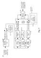
- FIG. 3 is a block diagram depicting a CATV return path 200 according to one embodiment of the present invention.
- an A/D converter 112 receives an analog return signal from a co-axial cable 201 and generates a stream of data at a full sampling rate (e.g., 100 MHz).
- a signal encoder 213 encodes the output of the A/D converter 112 and generates another stream of data at a lower data rate.
- the low data rate output of the signal encoder 213 is provided to the optical data transmitter 114 for transmission to a hub 220 as optical signals.
- the hub 220 can be an intermediate hub or a head end hub.
- an optical data receiver 122 receives the optical signals from the transmitter 210 and converts the signals to a low data rate data stream corresponding to the one generated by the signal encoder 213 .
- a signal decoder 223 receives and decodes the output of the optical data receiver 122 and generates a stream of data at a full sampling rate. The output of the decoder 223 is provided to the D/A converter 124 for conversion into analog signals.
- the signal encoder 213 and signal decoder 223 enable digital data to be transmitted across the optical link at a lower rate than N*F bits per second (where N is the number of bits and F is the sampling frequency of the A/D converter 112 ).
- N is the number of bits and F is the sampling frequency of the A/D converter 112
- the analog return signal carried by the co-axial cable 201 is an analog signal with signal components in a predefined frequency range, such as 5 to 42 MHz.
- FIG. 4 illustrates the spectral density of the signal components of a typical analog return signal.
- a typical sampling rate of the analog return signal is 100 MHz, which is higher than twice the highest frequency transmitted in the return path.
- users of the CATV return path only use specific portions of the return path spectrum. Thus, in those systems, only those portions of the return path spectrum carrying useful information need be transmitted from the node 210 to the hub 220 . Other portions of the return path spectrum can be filtered out.
- the desired signal is only in a portion of the return path spectrum approximately between 34 MHz and 40 MHz with a total bandwidth of approximately 6 MHz.
- the data rate of the optical link can be significantly reduced.
- the logic for transmitting a signal that embodies a specific portion of the return path spectrum is implemented in the encoder 213 .
- One implementation of the encoder 213 is shown in FIG. 5 .
- a stream of A/D samples at the Full Rate of 100 MHz is first filtered in a digital FIR (Finite Impulse Response) band-pass interpolation filter 510 to form a band-limited data stream.
- the filter rate of the band-pass interpolation filter 510 is chosen as a ratio of integers times the sample rate.
- Center Frequency of a bandpass filter refers to the frequency approximately at the center of the frequency band to be retained.
- the Center Frequency of the bandpass filter 510 in one embodiment, is chosen to be 6/17 of the Full Rate (100 MHz), which is approximately 35.29 MHz.
- A/D samples enter the filter at the Full Rate (e.g., 100 MHz), and samples are read from the multiple phase taps of band-pass interpolation filter 510 at a rate that is a multiple (e.g., four times) of the Center Frequency of the bandpass filter 510 to form another stream of samples.
- samples are read from the bass-pass interpolation filter 510 at a rate that is four times the Center Frequency. That is, in the present discussion, if the Center Frequency is 35.29 MHz, then samples are read from the band-pass interpolation filter 510 at a rate of 141.176 MHz.
- the data rate at which samples are read from the outputs of the bandpass interpolation filter 510 is set by an NCO (Numerically Controlled Oscillator) 512 .
- NCO Numerically Controlled Oscillator
- the rate at which samples are read from the outputs of the bandpass interpolation filter 510 can be unequal to four times of the Center Frequency.
- an analog input waveform of 33 MHz is shown in FIG. 7 .
- the 33 MHz analog waveform is sampled at 100 MHz, the resulting samples are shown in FIG. 8 .
- the coefficients of the FIR filter 510 with its Center Frequency at 35.3 MHz are shown in FIG. 9
- the filter response of the FIR filter 510 is shown in FIG. 10 .
- the 33 MHz waveform is sampled by interpolation by the FIR filter 510 at 141.176 MHz, the samples that make up a band-limited data stream are obtained.
- FIG. 11 depicts the band-limited data stream.
- the band-limited data stream is provided to digital multipliers 514 where it is separated into two data streams, one of which carries in-phase components and the other of which carries quadrature components.
- the data stream carrying the in-phase components is referred to as the in-phase data stream.
- the data stream carrying the quadrature components is referred to as the quadrature data stream.
- the separation is achieved by multiplying the band limited data stream by the cosine and sine waveforms whose frequency is the Center Frequency of the frequency band to be retained.
- the cosine and sine waveforms are generated by a sin/cos generator 516 at a data rate of the band-limited data stream.
- the cosine and sine waveforms are generated at a rate of four times the Center Frequency.
- the cosine waveform will include a stream of +10 ⁇ 10+10 ⁇ 10 . . .
- the sine waveform will include a stream of 0+10 ⁇ 10+10 ⁇ 1 . . . .
- Digital multiplication of the band-limited data stream by the cosine waveform results in a stream of in-phase components
- digital multiplication of the band-limited data stream by the sine waveform results in a stream of “quadrature” components.
- the in-phase and quadrature waveforms are illustrated in FIGS. 12 and 13 . Note that zeros are not output by the digital multipliers 514 .
- the data rate of the in-phase data stream 740 and that of the quadrature data stream 750 are approximately half of the data rate of the band-limited data stream 710 .
- the Center Frequency used by sin/cos generator 516 is generated by a numerically controlled oscillator (NCO) 518 .
- NCO numerically controlled oscillator
- the cosine and sine waveforms are generated by a look up table in memory or by other computational means.
- digital interpolation filters 520 up-sample the in-phase and quadrature data streams such that their outputs can be decimated accurately by a decimation filter 525 to a desired output rate.
- the output rate is generated by an NCO 524 , and decimation is accomplished by only sampling the output of the interpolation filters 520 at the desired output data rate.
- the desired output rate is at least twice the bandwidth of the desired frequency band. For example, if the bandwidth of the desired frequency band is 6 MHz, then the desired output rate is at least 12 MHz.
- the FIR filter coefficients for an example implementation of one of the digital interpolation filters 520 are shown in FIG. 14 .
- the digital interpolation filter 520 in 3 MHz lowpass interpolation filter.
- the frequency response of a 3 MHz lowpass interpolation filter is shown in FIG. 15 .
- the outputs of the digital interpolation filters 520 are decimated to a sample rate of 17.647 MHz.
- the decimated in-phase and quadrature data streams are illustrated in FIGS. 16 and 17 .
- the decimated data streams generated by the decimation filter 525 are then interleaved.
- the stream of interleaved samples is referred herein as the transport stream.
- the data rate of the transport stream therefore, is the sum of the data rates of the decimated in-phase and quadrature streams determined by decimation filter 525 .
- the transport stream is serialized by a SERDES circuit (not shown) and the resulting serial bit stream is used to drive the optical data transmitter 114 for generating optical signals for transmission to the hub 220 .
- FIG. 6 is a block diagram depicting an implementation of signal decoder 223 in accordance with an embodiment of the present invention.
- the signal decoder 223 is coupled to SERDES circuits of the optical data receiver 122 to receive the transport stream generated by node 210 .
- the transport stream consists of interleaved in-phase and quadrature components of the transmitted signal.
- the transport samples are first deinterleaved by deinterleaving logic 612 to form two separate streams one of which is the decimated in-phase stream and the other is the decimated quadrature stream. Then, the in-phase stream and the quadrature stream are filtered by interpolation filters 614 .
- the interpolation filters 614 are implemented in a similar fashion as interpolation filters 520 of the signal encoder 213 .
- the data rate at which samples are read from the outputs of the interpolation filters 614 is set by a NCO (Numerically Controlled Oscillator), which may be unequal to four times of the Center Frequency.
- FIGS. 18 and 19 are the upsampled in-phase and quadrature data streams of the example 33 MHz waveform, which are nearly the same as the waveforms of FIGS. 12 and 13 , differing only by computational errors.
- the interpolation filters 614 up-sample the in-phase stream and the quadrature stream such that they have a data rate at four times the Center Frequency of the desired frequency band. In other embodiments, the interpolation filters 614 up-sample the in-phase stream and the quadrature stream to sample rates that are not equal to four times the Center Frequency.
- the signal decoder 223 includes digital multipliers 618 , 619 and sin/cos generator 620 for generating sine and cosine waveforms.
- the sin/cos generator 620 receives the Center Frequency from the NCO 622 and generates cosine and sine waveforms at the Center Frequency.
- the cosine and sine waveforms are generated at a data rate four times the Center Frequency.
- the cosine waveform will include a stream of +10 ⁇ 10+10 ⁇ 10 . . .
- the sine waveform will include a stream of 0+10 ⁇ 10+10 ⁇ 1 . . . .
- the in-phase stream is multiplied by the cosine waveform and the quadrature stream is multiplied by the sine waveform.
- Digital multiplication of the stream in phase by the cosine waveform results in a stream of values with alternating zeros
- digital multiplication of the quadrature stream by the sine waveform results in another stream of values with alternating zeros.
- the outputs of the digital multipliers 618 , 619 are added in by digital adder 624 to generate yet another data stream whose data rate is four times the Center Frequency.
- the upsampled and combined samples of the example 33 MHz waveform are shown in FIG. 20 .
- the output of the digital adder 624 is processed by a bandpass interpolation filter 626 , which is constructed similarly to the bandpass interpolation filter 510 .
- the output of the bandpass interpolation filter 626 is decimated to an output data rate.
- the output data rate which is defined by NCO 628 , is the Full Rate (e.g., 100 MHz).
- the 100 mega-sample per second resampled output of the bandpass filter is shown in FIG.
- the digital samples output by the signal decoder 223 are sent to the D/A converter 124 to be converted to an analog signal.
- the analog signal thus recovered will have signal components within the desired frequency band.
- the output of the D/A converter with an analog low pass filter is the recovered analog wave form of FIG. 22 .
- the desired frequency band transmitted encompasses the full bandwidth of the input signal. That is, for a frequency band to be transmitted is 5 MHz to 42 MHz, and the Center Frequency is approximately 22.5 MHz. In other embodiments, the Center Frequency can be any frequency that is below one half of the frequency of the input data stream.
Abstract
Description
Claims (7)
Priority Applications (1)
| Application Number | Priority Date | Filing Date | Title |
|---|---|---|---|
| US13/170,098 US8863217B2 (en) | 2002-02-08 | 2011-06-27 | Bandpass component decimation and transmission of data in cable television digital return path |
Applications Claiming Priority (3)
| Application Number | Priority Date | Filing Date | Title |
|---|---|---|---|
| US35502302P | 2002-02-08 | 2002-02-08 | |
| US10/218,344 US7971225B2 (en) | 2002-02-08 | 2002-08-12 | Bandpass component decimation and transmission of data in cable television digital return path |
| US13/170,098 US8863217B2 (en) | 2002-02-08 | 2011-06-27 | Bandpass component decimation and transmission of data in cable television digital return path |
Related Parent Applications (1)
| Application Number | Title | Priority Date | Filing Date |
|---|---|---|---|
| US10/218,344 Continuation US7971225B2 (en) | 2002-02-08 | 2002-08-12 | Bandpass component decimation and transmission of data in cable television digital return path |
Publications (2)
| Publication Number | Publication Date |
|---|---|
| US20110255878A1 US20110255878A1 (en) | 2011-10-20 |
| US8863217B2 true US8863217B2 (en) | 2014-10-14 |
Family
ID=27668346
Family Applications (2)
| Application Number | Title | Priority Date | Filing Date |
|---|---|---|---|
| US10/218,344 Expired - Fee Related US7971225B2 (en) | 2002-02-08 | 2002-08-12 | Bandpass component decimation and transmission of data in cable television digital return path |
| US13/170,098 Expired - Lifetime US8863217B2 (en) | 2002-02-08 | 2011-06-27 | Bandpass component decimation and transmission of data in cable television digital return path |
Family Applications Before (1)
| Application Number | Title | Priority Date | Filing Date |
|---|---|---|---|
| US10/218,344 Expired - Fee Related US7971225B2 (en) | 2002-02-08 | 2002-08-12 | Bandpass component decimation and transmission of data in cable television digital return path |
Country Status (1)
| Country | Link |
|---|---|
| US (2) | US7971225B2 (en) |
Families Citing this family (8)
| Publication number | Priority date | Publication date | Assignee | Title |
|---|---|---|---|---|
| US20040103440A1 (en) * | 2002-11-25 | 2004-05-27 | General Instrument Corporation | Transmitter in a digital return link for use in an HFC network |
| US7698726B2 (en) * | 2004-01-27 | 2010-04-13 | General Instrument Corporation | Band limited port aggregation in a digital return path CATV system |
| US8687974B2 (en) * | 2011-01-22 | 2014-04-01 | Viasat, Inc. | Skew compensation and tracking in communications systems |
| US8693897B2 (en) | 2011-01-22 | 2014-04-08 | Viasat, Inc. | Digital demodulator architecture |
| CN108173596A (en) * | 2012-08-23 | 2018-06-15 | 菲尼萨公司 | For the integration laser and modulator transmitter of CATV applications |
| US9065566B1 (en) * | 2013-03-14 | 2015-06-23 | Arris Solutions, Inc. | Digitization and transport of return paths employing different frequency spectrums |
| US10237587B2 (en) * | 2016-06-10 | 2019-03-19 | Nokia Of America Corporation | Transporting out-of-band signals in distributed cable systems |
| US10979270B2 (en) * | 2018-03-09 | 2021-04-13 | Infinera Corporation | Scalable synthesis of signals of high symbol rate using lower symbol rate DSPS |
Citations (16)
| Publication number | Priority date | Publication date | Assignee | Title |
|---|---|---|---|---|
| US4048443A (en) * | 1975-12-12 | 1977-09-13 | Bell Telephone Laboratories, Incorporated | Digital speech communication system for minimizing quantizing noise |
| US4757390A (en) * | 1984-08-03 | 1988-07-12 | Deutsche Itt Industries Gmbh | Video recorder with a magnetic recording medium in the form of a tape |
| US4974236A (en) * | 1988-01-06 | 1990-11-27 | U.S. Philips Corporation | Arrangement for generating an SSB signal |
| US5282019A (en) * | 1988-10-03 | 1994-01-25 | Carlo Basile | Method and apparatus for the transmission and reception of a multicarrier digital television signal |
| US5600672A (en) * | 1991-03-27 | 1997-02-04 | Matsushita Electric Industrial Co., Ltd. | Communication system |
| US5949485A (en) * | 1991-01-17 | 1999-09-07 | Samsung Electronics Co., Ltd. | Method of compressing a video signal band transmission and device therefor |
| US5963557A (en) * | 1997-04-11 | 1999-10-05 | Eng; John W. | High capacity reservation multiple access network with multiple shared unidirectional paths |
| US6091932A (en) * | 1995-05-20 | 2000-07-18 | Regiocom Gmbh | Bidirectional point to multipoint network using multicarrier modulation |
| US6279158B1 (en) * | 1994-09-26 | 2001-08-21 | Adc Telecommunications, Inc. | Dynamic bandwidth allocation |
| US20020073434A1 (en) * | 2000-12-07 | 2002-06-13 | Macrodyne Power Llc | System and method for supporting broadband communications services |
| US20020131426A1 (en) * | 2000-06-22 | 2002-09-19 | Mati Amit | Scalable virtual channel |
| US6456657B1 (en) * | 1996-08-30 | 2002-09-24 | Bell Canada | Frequency division multiplexed transmission of sub-band signals |
| US6493005B1 (en) * | 1999-03-30 | 2002-12-10 | Sony Corporation | On screen display |
| US20030016701A1 (en) * | 2001-07-23 | 2003-01-23 | Hinson Scott R. | Distributed block frequency converter |
| US6724832B1 (en) * | 1999-01-29 | 2004-04-20 | Adc Broadband Wireless Group, Inc. | Vestigial sideband generator particularly for digital television |
| US6724439B1 (en) * | 2000-08-04 | 2004-04-20 | Zenith Electronics Corporation | Low cost VSB encoder and RF modulator for supplying a substantially 6 MHZ VSB signal to digital television receiver |
Family Cites Families (47)
| Publication number | Priority date | Publication date | Assignee | Title |
|---|---|---|---|---|
| US5235619A (en) | 1990-03-20 | 1993-08-10 | Scientific-Atlanta, Inc. | Cable television radio frequency subscriber data transmission apparatus and rf return method |
| US5014309A (en) | 1988-03-10 | 1991-05-07 | Scientific-Atlanta, Inc. | Off-premises cable television channel interdiction method and apparatus |
| US5208854A (en) | 1988-03-10 | 1993-05-04 | Scientific-Atlanta, Inc. | Picture carrier controlled automatic gain control circuit for cable television interdiction or jamming apparatus |
| US5303295A (en) | 1988-03-10 | 1994-04-12 | Scientific-Atlanta, Inc. | Enhanced versatility of a program control by a combination of technologies |
| US5319454A (en) | 1990-11-13 | 1994-06-07 | Scientific-Atlanta, Inc. | CATV system enabling access to premium (pay per view) program events by bar code data entry |
| US5155590A (en) | 1990-03-20 | 1992-10-13 | Scientific-Atlanta, Inc. | System for data channel level control |
| US5323462A (en) | 1988-03-10 | 1994-06-21 | Scientific-Atlanta, Inc. | CATV subscriber disconnect switch |
| US5505901A (en) | 1988-03-10 | 1996-04-09 | Scientific-Atlanta, Inc. | CATV pay per view interdiction system method and apparatus |
| US5251324A (en) | 1990-03-20 | 1993-10-05 | Scientific-Atlanta, Inc. | Method and apparatus for generating and collecting viewing statistics for remote terminals in a cable television system |
| US5142690A (en) | 1990-03-20 | 1992-08-25 | Scientific-Atlanta, Inc. | Cable television radio frequency data processor |
| US5225902A (en) | 1990-03-20 | 1993-07-06 | Scientific-Atlanta, Inc. | Automatic frequency selection in a bi-directional cable television system |
| US5255086A (en) | 1990-03-20 | 1993-10-19 | Scientific-Atlanta, Inc. | Method and apparatus for RF data transfer in a CATV system |
| US5245420A (en) | 1990-11-27 | 1993-09-14 | Scientific-Atlanta, Inc. | CATV pay per view interdiction system |
| US5113189A (en) | 1991-06-21 | 1992-05-12 | Motorola, Inc. | Frequency translating coherent analog to digital conversion system for modulated signals |
| AU661339B2 (en) | 1991-09-03 | 1995-07-20 | Scientific-Atlanta, Inc. | Fiber optic status monitor and control system |
| US5317391A (en) | 1991-11-29 | 1994-05-31 | Scientific-Atlanta, Inc. | Method and apparatus for providing message information to subscribers in a cable television system |
| US5247364A (en) | 1991-11-29 | 1993-09-21 | Scientific-Atlanta, Inc. | Method and apparatus for tuning data channels in a subscription television system having in-band data transmissions |
| US5497187A (en) | 1991-11-29 | 1996-03-05 | Scientific-Atlanta, Inc. | In-band/out-of-band data transmission method and apparatus for a television system |
| US5301028A (en) | 1991-11-29 | 1994-04-05 | Scientific-Atlanta, Inc. | Method and apparatus for displaying channel identification information |
| US5243651A (en) | 1992-06-10 | 1993-09-07 | Scientific-Atlanta, Inc. | Diagnostic method and apparatus for a cable television interdiction system |
| US5430568A (en) | 1992-12-01 | 1995-07-04 | Scientific-Atlanta, Inc. | Optical communications system for transmitting information signals having different wavelengths over a same optical fiber |
| US5357276A (en) | 1992-12-01 | 1994-10-18 | Scientific-Atlanta, Inc. | Method of providing video on demand with VCR like functions |
| US5499241A (en) | 1993-09-17 | 1996-03-12 | Scientific-Atlanta, Inc. | Broadband communications system |
| US5581555A (en) | 1993-09-17 | 1996-12-03 | Scientific-Atlanta, Inc. | Reverse path allocation and contention resolution scheme for a broadband communications system |
| US5594726A (en) | 1993-09-17 | 1997-01-14 | Scientific-Atlanta, Inc. | Frequency agile broadband communications system |
| US5539822A (en) | 1994-04-19 | 1996-07-23 | Scientific-Atlanta, Inc. | System and method for subscriber interactivity in a television system |
| CA2199815C (en) | 1994-09-12 | 2001-07-24 | Catherine W. Jelinek | Cable television apparatus employing two-way communication |
| US5742591A (en) * | 1995-06-07 | 1998-04-21 | General Instrument Corporation | Interference cancellation system for CATV return transmissions |
| EP0873638B1 (en) | 1995-06-22 | 2010-08-04 | Scientific Atlanta, Inc. | Hybrid fiber coax communications system |
| US5930231A (en) | 1995-06-30 | 1999-07-27 | Scientific-Atlanta, Inc. | Block spectrum receiver for a broadband communications system |
| US5719867A (en) | 1995-06-30 | 1998-02-17 | Scientific-Atlanta, Inc. | Plural telephony channel baseband signal demodulator for a broadband communications system |
| US6272150B1 (en) | 1997-01-17 | 2001-08-07 | Scientific-Atlanta, Inc. | Cable modem map display for network management of a cable data delivery system |
| US5963352A (en) | 1997-02-21 | 1999-10-05 | Scientific-Atlanta, Inc. | Linearization enhanced operation of single-stage and dual-stage electro-optic modulators |
| US5854703A (en) | 1997-02-28 | 1998-12-29 | Scientific-Atlanta, Inc. | Hybrid fiber coax communications network |
| US6457178B1 (en) | 1998-03-17 | 2002-09-24 | Scientific-Atlanta, Inc. | Pulse width modulator for communication system including fiber optic communications |
| US6449071B1 (en) | 1998-06-22 | 2002-09-10 | Scientific-Atlanta, Inc. | Digital signal processing optical transmitter |
| US6373611B1 (en) | 1998-06-22 | 2002-04-16 | Scientific-Atlanta, Inc. | Digital optical transmitter |
| US6356374B1 (en) | 1998-10-09 | 2002-03-12 | Scientific-Atlanta, Inc. | Digital optical transmitter |
| US6751269B1 (en) | 1999-01-11 | 2004-06-15 | Texas Instruments Incorporated | Bit-interleaved coded modulation for CATV upstream channels |
| US6356369B1 (en) | 1999-02-22 | 2002-03-12 | Scientific-Atlanta, Inc. | Digital optical transmitter for processing externally generated information in the reverse path |
| US6523177B1 (en) | 1999-04-01 | 2003-02-18 | Scientific-Atlanta, Inc. | Cable television system with digital reverse path architecture |
| US6437895B1 (en) | 1999-04-05 | 2002-08-20 | Scientific-Atlanta, Inc. | Digital optical transmitter with compression |
| DE10030407B4 (en) | 1999-07-14 | 2011-09-01 | Lg Electronics Inc. | Method for optimal rate adaptation in a mobile communication system |
| US6433906B1 (en) | 1999-09-22 | 2002-08-13 | Scientific-Atlanta, Inc. | Digital optical receiver for cable television systems |
| US6417949B1 (en) | 1999-11-05 | 2002-07-09 | Scientific-Atlanta, Inc. | Broadband communication system for efficiently transmitting broadband signals |
| JP2002043965A (en) | 2000-07-31 | 2002-02-08 | Pioneer Electronic Corp | Receiver |
| US6462851B1 (en) | 2001-04-23 | 2002-10-08 | Scientific-Atlanta, Inc. | Network and method for transmitting reverse analog signals by sub-sampling the digital reverse bandwidth |
-
2002
- 2002-08-12 US US10/218,344 patent/US7971225B2/en not_active Expired - Fee Related
-
2011
- 2011-06-27 US US13/170,098 patent/US8863217B2/en not_active Expired - Lifetime
Patent Citations (16)
| Publication number | Priority date | Publication date | Assignee | Title |
|---|---|---|---|---|
| US4048443A (en) * | 1975-12-12 | 1977-09-13 | Bell Telephone Laboratories, Incorporated | Digital speech communication system for minimizing quantizing noise |
| US4757390A (en) * | 1984-08-03 | 1988-07-12 | Deutsche Itt Industries Gmbh | Video recorder with a magnetic recording medium in the form of a tape |
| US4974236A (en) * | 1988-01-06 | 1990-11-27 | U.S. Philips Corporation | Arrangement for generating an SSB signal |
| US5282019A (en) * | 1988-10-03 | 1994-01-25 | Carlo Basile | Method and apparatus for the transmission and reception of a multicarrier digital television signal |
| US5949485A (en) * | 1991-01-17 | 1999-09-07 | Samsung Electronics Co., Ltd. | Method of compressing a video signal band transmission and device therefor |
| US5600672A (en) * | 1991-03-27 | 1997-02-04 | Matsushita Electric Industrial Co., Ltd. | Communication system |
| US6279158B1 (en) * | 1994-09-26 | 2001-08-21 | Adc Telecommunications, Inc. | Dynamic bandwidth allocation |
| US6091932A (en) * | 1995-05-20 | 2000-07-18 | Regiocom Gmbh | Bidirectional point to multipoint network using multicarrier modulation |
| US6456657B1 (en) * | 1996-08-30 | 2002-09-24 | Bell Canada | Frequency division multiplexed transmission of sub-band signals |
| US5963557A (en) * | 1997-04-11 | 1999-10-05 | Eng; John W. | High capacity reservation multiple access network with multiple shared unidirectional paths |
| US6724832B1 (en) * | 1999-01-29 | 2004-04-20 | Adc Broadband Wireless Group, Inc. | Vestigial sideband generator particularly for digital television |
| US6493005B1 (en) * | 1999-03-30 | 2002-12-10 | Sony Corporation | On screen display |
| US20020131426A1 (en) * | 2000-06-22 | 2002-09-19 | Mati Amit | Scalable virtual channel |
| US6724439B1 (en) * | 2000-08-04 | 2004-04-20 | Zenith Electronics Corporation | Low cost VSB encoder and RF modulator for supplying a substantially 6 MHZ VSB signal to digital television receiver |
| US20020073434A1 (en) * | 2000-12-07 | 2002-06-13 | Macrodyne Power Llc | System and method for supporting broadband communications services |
| US20030016701A1 (en) * | 2001-07-23 | 2003-01-23 | Hinson Scott R. | Distributed block frequency converter |
Also Published As
| Publication number | Publication date |
|---|---|
| US7971225B2 (en) | 2011-06-28 |
| US20030154494A1 (en) | 2003-08-14 |
| US20110255878A1 (en) | 2011-10-20 |
Similar Documents
| Publication | Publication Date | Title |
|---|---|---|
| US8863217B2 (en) | Bandpass component decimation and transmission of data in cable television digital return path | |
| US5553064A (en) | High speed bidirectional digital cable transmission system | |
| US5596609A (en) | Parallel cascaded integrator-comb filter | |
| US5937341A (en) | Simplified high frequency tuner and tuning method | |
| US7570723B2 (en) | Multiple input, multiple output channel, digital receiver tuner | |
| EP0524229B1 (en) | Signal distribution | |
| US6741650B1 (en) | Architecture for intermediate frequency encoder | |
| US20090290602A1 (en) | Apparatus and method for frequency translation | |
| US8509342B2 (en) | System and method for delivery of video, content on demand and IP packets | |
| US6301312B1 (en) | Bandpass phase tracker with hilbert transformation before analog-to-digital conversion | |
| US6437895B1 (en) | Digital optical transmitter with compression | |
| KR0176643B1 (en) | Digital vsb detector with bandpass phase tracker using radear filters, as for use in an hdtv receiver | |
| US8156535B2 (en) | Data rate compression device for cable television return path using bandpass puncturing | |
| US6975685B1 (en) | Apparatus and method for multi-channel communications system | |
| US6570942B2 (en) | Multi-mode variable rate digital cable receiver | |
| US6621366B1 (en) | Parallel-process digital modulator structures and methods | |
| WO2001097420A2 (en) | Multiplexing digital communication system | |
| US7656332B2 (en) | Method and apparatus for a multi-mode multi-rate telemetry transmitter | |
| US8184210B2 (en) | Digital Radio Frequency (RF) Modulator | |
| US20070047673A1 (en) | Intermediate frequency receivers | |
| US7751718B2 (en) | Efficient transmission of digital return path data in cable television return path | |
| CN1856942A (en) | Receiver and method for concurrent receiving of multiple channels | |
| Langston | Local Multipoint Distribution Services (LMDS) system concepts and implementation | |
| US20040165672A1 (en) | Upstream communication system with controllable band pass filter properties | |
| KR20110071424A (en) | Receiving system receving radio frequency signal to convert into baseband signal |
Legal Events
| Date | Code | Title | Description |
|---|---|---|---|
| AS | Assignment |
Owner name: FINISAR CORPORATION, CALIFORNIA Free format text: ASSIGNMENT OF ASSIGNORS INTEREST;ASSIGNOR:SAGE, GERALD FRANCIS;REEL/FRAME:033742/0795 Effective date: 20020807 |
|
| STCF | Information on status: patent grant |
Free format text: PATENTED CASE |
|
| MAFP | Maintenance fee payment |
Free format text: PAYMENT OF MAINTENANCE FEE, 4TH YEAR, LARGE ENTITY (ORIGINAL EVENT CODE: M1551) Year of fee payment: 4 |
|
| AS | Assignment |
Owner name: BANK OF AMERICA, N.A., AS ADMINISTRATIVE AGENT, NO Free format text: NOTICE OF GRANT OF SECURITY INTEREST IN PATENTS;ASSIGNORS:II-VI INCORPORATED;MARLOW INDUSTRIES, INC.;EPIWORKS, INC.;AND OTHERS;REEL/FRAME:050484/0204 Effective date: 20190924 Owner name: BANK OF AMERICA, N.A., AS ADMINISTRATIVE AGENT, NORTH CAROLINA Free format text: NOTICE OF GRANT OF SECURITY INTEREST IN PATENTS;ASSIGNORS:II-VI INCORPORATED;MARLOW INDUSTRIES, INC.;EPIWORKS, INC.;AND OTHERS;REEL/FRAME:050484/0204 Effective date: 20190924 |
|
| AS | Assignment |
Owner name: II-VI DELAWARE, INC., DELAWARE Free format text: ASSIGNMENT OF ASSIGNORS INTEREST;ASSIGNOR:FINISAR CORPORATION;REEL/FRAME:052286/0001 Effective date: 20190924 |
|
| MAFP | Maintenance fee payment |
Free format text: PAYMENT OF MAINTENANCE FEE, 8TH YEAR, LARGE ENTITY (ORIGINAL EVENT CODE: M1552); ENTITY STATUS OF PATENT OWNER: LARGE ENTITY Year of fee payment: 8 |
|
| AS | Assignment |
Owner name: JPMORGAN CHASE BANK, N.A., AS COLLATERAL AGENT, NEW YORK Free format text: SECURITY INTEREST;ASSIGNORS:II-VI INCORPORATED;II-VI DELAWARE, INC.;M CUBED TECHNOLOGIES, INC.;AND OTHERS;REEL/FRAME:060562/0254 Effective date: 20220701 |
|
| AS | Assignment |
Owner name: PHOTOP TECHNOLOGIES, INC., CALIFORNIA Free format text: PATENT RELEASE AND REASSIGNMENT;ASSIGNOR:BANK OF AMERICA, N.A., AS ADMINISTRATIVE AGENT;REEL/FRAME:060574/0001 Effective date: 20220701 Owner name: II-VI OPTOELECTRONIC DEVICES, INC., NEW JERSEY Free format text: PATENT RELEASE AND REASSIGNMENT;ASSIGNOR:BANK OF AMERICA, N.A., AS ADMINISTRATIVE AGENT;REEL/FRAME:060574/0001 Effective date: 20220701 Owner name: II-VI DELAWARE, INC., PENNSYLVANIA Free format text: PATENT RELEASE AND REASSIGNMENT;ASSIGNOR:BANK OF AMERICA, N.A., AS ADMINISTRATIVE AGENT;REEL/FRAME:060574/0001 Effective date: 20220701 Owner name: II-VI PHOTONICS (US), INC., MASSACHUSETTS Free format text: PATENT RELEASE AND REASSIGNMENT;ASSIGNOR:BANK OF AMERICA, N.A., AS ADMINISTRATIVE AGENT;REEL/FRAME:060574/0001 Effective date: 20220701 Owner name: M CUBED TECHNOLOGIES, INC., CONNECTICUT Free format text: PATENT RELEASE AND REASSIGNMENT;ASSIGNOR:BANK OF AMERICA, N.A., AS ADMINISTRATIVE AGENT;REEL/FRAME:060574/0001 Effective date: 20220701 Owner name: II-VI OPTICAL SYSTEMS, INC., CALIFORNIA Free format text: PATENT RELEASE AND REASSIGNMENT;ASSIGNOR:BANK OF AMERICA, N.A., AS ADMINISTRATIVE AGENT;REEL/FRAME:060574/0001 Effective date: 20220701 Owner name: FINISAR CORPORATION, CALIFORNIA Free format text: PATENT RELEASE AND REASSIGNMENT;ASSIGNOR:BANK OF AMERICA, N.A., AS ADMINISTRATIVE AGENT;REEL/FRAME:060574/0001 Effective date: 20220701 Owner name: OPTIUM CORPORATION, CALIFORNIA Free format text: PATENT RELEASE AND REASSIGNMENT;ASSIGNOR:BANK OF AMERICA, N.A., AS ADMINISTRATIVE AGENT;REEL/FRAME:060574/0001 Effective date: 20220701 Owner name: COADNA PHOTONICS, INC., PENNSYLVANIA Free format text: PATENT RELEASE AND REASSIGNMENT;ASSIGNOR:BANK OF AMERICA, N.A., AS ADMINISTRATIVE AGENT;REEL/FRAME:060574/0001 Effective date: 20220701 Owner name: KAILIGHT PHOTONICS, INC., CALIFORNIA Free format text: PATENT RELEASE AND REASSIGNMENT;ASSIGNOR:BANK OF AMERICA, N.A., AS ADMINISTRATIVE AGENT;REEL/FRAME:060574/0001 Effective date: 20220701 Owner name: LIGHTSMYTH TECHNOLOGIES, INC., OREGON Free format text: PATENT RELEASE AND REASSIGNMENT;ASSIGNOR:BANK OF AMERICA, N.A., AS ADMINISTRATIVE AGENT;REEL/FRAME:060574/0001 Effective date: 20220701 Owner name: EPIWORKS, INC., ILLINOIS Free format text: PATENT RELEASE AND REASSIGNMENT;ASSIGNOR:BANK OF AMERICA, N.A., AS ADMINISTRATIVE AGENT;REEL/FRAME:060574/0001 Effective date: 20220701 Owner name: MARLOW INDUSTRIES, INC., TEXAS Free format text: PATENT RELEASE AND REASSIGNMENT;ASSIGNOR:BANK OF AMERICA, N.A., AS ADMINISTRATIVE AGENT;REEL/FRAME:060574/0001 Effective date: 20220701 Owner name: II-VI INCORPORATED, PENNSYLVANIA Free format text: PATENT RELEASE AND REASSIGNMENT;ASSIGNOR:BANK OF AMERICA, N.A., AS ADMINISTRATIVE AGENT;REEL/FRAME:060574/0001 Effective date: 20220701 |