US8861407B2 - Multiple connection options for a transceiver - Google Patents
Multiple connection options for a transceiver Download PDFInfo
- Publication number
- US8861407B2 US8861407B2 US13/177,574 US201113177574A US8861407B2 US 8861407 B2 US8861407 B2 US 8861407B2 US 201113177574 A US201113177574 A US 201113177574A US 8861407 B2 US8861407 B2 US 8861407B2
- Authority
- US
- United States
- Prior art keywords
- duplexer
- substrate
- aperture
- pads
- interconnection pads
- Prior art date
- Legal status (The legal status is an assumption and is not a legal conclusion. Google has not performed a legal analysis and makes no representation as to the accuracy of the status listed.)
- Active, expires
Links
Images


Classifications
-
- H—ELECTRICITY
- H01—ELECTRIC ELEMENTS
- H01P—WAVEGUIDES; RESONATORS, LINES, OR OTHER DEVICES OF THE WAVEGUIDE TYPE
- H01P1/00—Auxiliary devices
- H01P1/20—Frequency-selective devices, e.g. filters
- H01P1/213—Frequency-selective devices, e.g. filters combining or separating two or more different frequencies
-
- H—ELECTRICITY
- H01—ELECTRIC ELEMENTS
- H01L—SEMICONDUCTOR DEVICES NOT COVERED BY CLASS H10
- H01L2924/00—Indexing scheme for arrangements or methods for connecting or disconnecting semiconductor or solid-state bodies as covered by H01L24/00
- H01L2924/19—Details of hybrid assemblies other than the semiconductor or other solid state devices to be connected
- H01L2924/191—Disposition
- H01L2924/19101—Disposition of discrete passive components
- H01L2924/19107—Disposition of discrete passive components off-chip wires
Definitions
- the present invention relates generally to transceivers, and specifically to differing ways for connecting microwave transceivers.
- Microwave transceivers typically operate over a range of frequencies. In some cases, different transceivers may be required depending on the receive or transmit frequency, or frequency band, at which the transceivers are to operate. Such a requirement for different transceivers uses resources inefficiently.
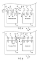
- FIGS. 1 , 2 , 3 , 4 are schematic top views of portions of a substrate, according to embodiments of the present invention.
- FIGS. 5 , 6 , 7 , 8 are schematic top views of portions of a substrate, according to alternative embodiments of the present invention.
- FIG. 9 is a schematic perspective view of a portion of a substrate, according to a further alternative embodiment of the present invention.
- FIG. 10 is a schematic perspective view of a portion of a substrate, according to a yet further embodiment of the present invention.
- FIG. 11 shows schematic diagrams of top views of a portion of a substrate, according to another embodiment of the present invention.
- FIG. 12 shows schematic diagrams of top views of portions of a microwave transceiver, according to an embodiment of the present invention.
- a communication device typically a receiver or a transmitter, has two or more radio frequency (RF) ports for communicating in respective electromagnetic (EM) frequency bands.
- the communication device may be mounted on a substrate having device interconnection ports in the form of radiative antennas, typically radiation launch pads or patch antennas, respectively connected to the RF ports of the device.
- a duplexer may be attached to the substrate in such a way as to transfer EM radiation via one of the interconnection ports, and thus via one of the RF ports operative at a selected frequency band.
- a transceiver comprises two of the communication devices described above: a transmitter communication device having two or more transmit RF ports, and a receiver communication device having two or more receive RF ports (corresponding in number to the transmit ports).
- the devices are typically mounted on a substrate.
- Each transmit port may be connected to a respective transmit interconnection port that is mounted on the substrate, and each receive port may be connected to a respective receive interconnection port mounted on the substrate.
- Each pair of transmit and receive ports is typically operative at a different frequency band.
- a duplexer is selected from a group of duplexers, the selected duplexer coupling a particular pair of transmit and receive interconnection ports to an antenna.
- the coupling to the antenna is via an aperture in the substrate that is common for all the duplexers in the group.
- the transceiver is thus configured to operate at a particular frequency band by selection and coupling of a duplexer.
- one device interconnection port may be selectably connected to one of a number of RF ports of a communication device.
- the device and the one interconnection port are typically located on a substrate, and the selection of the RF port may be performed by attaching one of a group of dielectric plates to the substrate.
- Each dielectric plate comprises a conducting line that connects a selected RF port to the interconnection port.
- each of the dielectric plates in the group is formed with an interconnection port.
- a particular RF port may be chosen for operation by attachment of a selected dielectric plate to the substrate.
- FIGS. 1-4 are schematic top views of portions of a substrate 20 , according to embodiments of the present invention.
- Substrate 20 acts as a scaffold upon which are mounted elements that are typically configured to form a microwave transceiver 22 .
- substrate 20 is assumed to comprise a printed circuit board (PCB), and is herein also referred to as PCB 20 .
- PCB 20 typically comprises a solid dielectric sheet, the top and bottom surfaces of which are at least partially covered by a conductor such as copper, so that the PCB is a double-layered PCB.
- substrate 20 may be configured as a multi-layered PCB, having one or more conducting layers interleaved in the solid dielectric sheet in addition to conductors on the top and bottom surfaces.
- Microwave transceiver 22 is assumed to operate within a radio frequency (RF) range between approximately GHz and approximately 40 GHz. However, there is no requirement that transceiver 22 operates within this range, so that embodiments of the present invention may operate at frequencies above or below the range.
- RF radio frequency
- Transceiver 22 comprises a transmitter communication device 24 formed as an integrated circuit (IC) mounted on the top surface of PCB 20 .
- transmitter device 24 comprises a modular microwave IC (MMIC).
- MMIC modular microwave IC
- Transmitter 24 is configured to transmit electromagnetic (EM) energy in a selectable one of a number of frequency ranges, herein for simplicity also referred to as transmit frequencies, or just frequencies.
- Transmitter 24 is, by way of example, assumed to transmit three frequencies designated T 1 , T 2 , and T 3 .
- the frequency at which the transmitter transmits may typically be selected by an operator or producer of transceiver 22 .
- the EM energy in the different frequencies is transmitted via separate, generally similar, guided transmission lines 26 , 28 , 30 from respective output transmit RF ports TP 1 , TP 2 , and TP 3 of the transmitter. Except where otherwise indicated, in the following description lines 26 , 28 , 30 and other guided transmission lines referred to herein are assumed, by way of example, to be formed as microstrips on substrate 20 , i.e., as conducting lines separated from a conducting ground layer by the dielectric sheet of the substrate, so that lines such as line 26 may also be referred to herein as microstrip 26 .
- Microstrips 26 , 28 , 30 respectively terminate at connectors 32 , 34 , 36 .
- the connectors are configured to accept respective transmit power amplifiers, so that the amplifiers, when installed in the connectors, receive their input EM energy from the microstrips.
- Microstrips 26 , 28 , 30 thus act as input lines to the connectors.
- Connectors 32 , 34 , 36 also have respective output lines, in the form of microstrips 38 , 40 , 42 , which convey the amplified EM energy output by the power amplifiers to respective transmission interconnection ports 44 , 46 , 48 , herein also referred to as launch pads, at which the output lines terminate.
- Launch pads 44 , 46 , 48 are typically configured as patch antennas that radiate the amplified EM energy received from their microstrips. Typically, dimensions of the pads are selected to optimize the radiation efficiency of the pad for the frequency at which it operates. The location of each of the transmission launch pads on substrate 20 is described below.
- Transceiver 22 also comprises a receiver communication device 64 , which is formed as an integrated circuit, in some embodiments an MMIC, mounted on the top surface of PCB 20 .
- Receiver 64 is typically configured to receive EM energy at the same number of frequencies as transmitter 24 , so that in the example described herein, the receiver receives at a selectable one of three receive frequency ranges R 1 , R 2 , R 3 , corresponding to frequency ranges T 1 , T 2 , T 3 of the transmitter.
- the receive frequency ranges are also referred to herein as frequencies.
- each pair of frequencies (T 1 , R 1 ), (T 2 , R 2 ), and (T 3 , R 3 ) is different, although in some embodiments, such as, for example, in a time division duplex (TDD) system, the frequencies of each pair may be the same.
- TDD time division duplex
- pairs of frequencies (T 1 , R 1 ), (T 2 , R 2 ), and (T 3 , R 3 ) are respectively selected to correspond to industry recognized frequency bands, herein referred to as B 1 , B 2 , B 3 .
- Table I illustrates examples of industry recognized frequencies for bands B 1 , B 2 , and B 3 .
- Frequencies R 1 , R 2 , R 3 are collected at respective receive interconnection ports 74 , 76 , 78 , also referred to herein as receive launch pads, which as for the transmission pads, are typically configured as patch antennas.
- the dimensions of each receive launch pad are typically also selected to optimize the radiation efficiency of the pad at the frequency (R 1 , R 2 , or R 3 ) at which it operates.
- Launch pads 74 , 76 , 78 are respectively connected to input RF ports RP 1 , RP 2 , and RP 3 of receiver 64 by lines 80 , 82 , 84 . The location of each of the receive launch pads is described below.
- Substrate 20 comprises a common aperture 86 via which the three transmit and three receive frequencies of transceiver 22 transfer.
- the aperture is connected by a guided transmission line to an antenna, typically a horn or parabolic dish antenna, which is designed to operate efficiently at the transmit and receive frequencies.
- an antenna typically a horn or parabolic dish antenna, which is designed to operate efficiently at the transmit and receive frequencies.
- the antenna and the transmission line connecting aperture 86 to the antenna are not shown in the figures.
- the transmit and receive frequencies of a given frequency band are transferred to and from aperture 86 via a respective duplexer.
- transceiver 22 there are separate duplexers 88 , 90 , 92 for each frequency band.
- the group of duplexers 88 , 90 , 92 are formed of transmission lines such as waveguides.
- the waveguides have appropriate isolators and/or circulators, acting as directional filters, installed to ensure minimal crossover between the transmit and receive signals.
- the isolators/circulators are not shown in FIGS. 2-4 .
- the locations of the transmission and receive launch pads on substrate 20 are selected so that each duplexer aligns with a specific pair of pads, and so that an opening of each duplexer aligns with aperture 86 .
- duplexer 88 ( FIG. 2 ), which is used for frequency band B 3 , has an antenna opening 94 aligning with aperture 86 , and the antenna opening has dimensions so that it mates with the aperture.
- duplexer has a transmit opening 96 aligning with and dimensioned to mate with transmission launch pad 48 , and a receive opening 98 aligning with and dimensioned to mate with receive launch pad 78 .
- duplexers 90 and 92 ( FIGS. 3 and 4 ), have respective antenna openings 100 , 102 aligning with and dimensioned to mate with aperture 86 .
- Duplexer 90 is used for frequency band B 2
- duplexer 92 is used for band B 1 .
- Duplexers 90 and 92 have respective transmit openings 104 , 106 aligning with and dimensioned to mate with transmission launch pads 46 and 44 , and respective receive openings 108 , 110 aligning with and dimensioned to mate with receive launch pads 76 and 74 .
- an assembler To assemble transceiver 22 , an assembler first chooses the frequency band at which the transceiver is to operate, and selects the appropriate duplexer from the group of duplexers 88 , 90 , and 92 .
- the selected duplexer is attached to substrate 20 , as illustrated in FIGS. 2-4 .
- the attachment is typically mechanical, such as is provided by screws and/or spring clips, but may also comprise at least partially attaching by soldering or welding.
- an appropriate transmit power amplifier, PA 1 , PA 2 , or PA 3 is chosen and inserted into one of connectors 32 , 34 , 36 .
- the power amplifiers may be incorporated into the assembly in any other way known in the art, such as by soldering or attaching by screws.
- the selected power amplifier PA 1 , PA 2 , or PA 3 is specific to the transmit frequency T 1 , T 2 , or T 3 . In some embodiments, one power amplifier may be used for more than one transmit frequency.
- FIGS. 5-8 are schematic top views of a portion of a substrate 220 upon which is formed a microwave transceiver 222 , according to embodiments of the present invention.
- the operation of transceiver 222 is generally similar to that of transceiver 22 ( FIGS. 1-4 ), and substrate 220 is substantially similar in properties and function to substrate 20 , so that apart from the differences described below, elements indicated by the same reference numerals in both transceivers 22 and 222 are generally similar in construction and in operation.
- Transceiver 222 is, like transceiver 22 , configured to be operable in one of a number of frequency bands. As for transceiver 22 , transceiver 222 is assumed by way of example to be able to operate in one of three different bands B 1 , B 2 , or B 3 , using transmit ports TP 1 , TP 2 , TP 3 , of transmitter 24 and receive ports RP 1 , RP 2 , RP 3 , of receiver 64 .
- Transceiver 222 is typically configured to be able to operate at any one of bands B 1 , B 2 , or B 3 by positioning respective duplexers 224 A, 224 B, or 224 C on the transceiver.
- Duplexers 224 A, 224 B, and 224 C are respectively operative over bands B 1 , B 2 , and B 3 , and typically have the same size. Alternatively, depending on the frequencies of the bands, a single duplexer may operate over two or all three of the bands.
- duplexers 224 A, 224 B, and 224 C are also referred to collectively as duplexers 224 .
- transceiver 222 comprises substantially similar operational elements to those of transceiver 22 , from a conceptual point of view the elements in transceiver 222 may be considered to be repositioned, i.e., located and/or oriented differently, compared to those of transceiver 22 .
- the conceptual repositioning of the elements of transceiver 222 is assumed to be implemented by a counter-clockwise rotation by 90° of transmitter 24 and its coupled elements relative to the position of the transmitter and elements in transceiver 22 .
- receiver 64 and its coupled elements comprises a clockwise rotation by 90° of receiver 64 and its coupled elements relative to the position of the receiver and elements in transceiver 22 , followed by a reflection of the receiver and its coupled elements in a horizontal line of symmetry.
- transceiver 222 is typically implemented as illustrated in FIGS. 5-8 , with no actual repositioning of elements of transceiver 22 .
- launch pads 44 and 74 , launch pads 46 and 76 , and launch pads 48 and 78 are arranged to be substantially equal.
- the launch pads are arranged on substrate 220 so that lines joining the launch pads, shown in FIG. 5 as broken lines 226 , 228 , and 230 , cross at a common intersection.
- an aperture 232 is formed in substrate 220 , aperture 232 having substantially the same function as aperture 86 of transceiver 22 .
- launch pads 44 and 74 , 46 and 76 , and 48 and 78 are aligned so that, as illustrated in FIGS. 5-8 , they are approximately orthogonal to their joining lines.
- Duplexers 224 function and are constructed generally as duplexers 88 , 90 , and 92 , serving to isolate transmitter 24 and receiver 64 from each other, while allowing each communication device to perform correctly.
- Duplexers 224 comprise a central antenna opening 234 , a transmit opening 236 , and a receive opening 238 .
- transceiver 222 To assemble transceiver 222 , the frequency band at which the transceiver is to operate is chosen, and an appropriate power amplifier, PA 1 , PA 2 , or PA 3 is connected into the transceiver, for example, by inserting it into its socket.
- Duplexer 224 A, 224 B, or 224 C is then positioned so that opening 234 aligns with aperture 232 , so that the transmit opening aligns with the transmission launch pad of the chosen frequency band, and so that the receive opening aligns with the band's receive launch pad.
- duplexer 224 A, 224 B, or 224 C is attached to substrate 220 , generally as described above for duplexers 88 , 90 , and 92 .
- FIG. 6 illustrates transceiver 222 assembled to operate in frequency band B 1 .
- Amplifier PA 1 is inserted into connection 32 and openings 236 and 238 respectively align with pads 44 and 74 .
- FIG. 7 illustrates the transceiver assembled to operate in frequency band B 2 .
- Amplifier PA 2 is inserted into connection 34 ; openings 236 and 238 align with pads 46 and 76 .
- FIG. 8 illustrates the transceiver assembled to operate in frequency band B 3 .
- Amplifier PA 3 is inserted into connection 36 and openings 236 and 238 respectively align with pads 48 and 78 .
- FIG. 9 is a schematic perspective view of a portion of a substrate 300 upon which is formed a microwave transceiver 302 , according to an embodiment of the present invention.
- the operation of transceiver 302 is generally similar to that of transceiver 22 ( FIGS. 1-4 ), and substrate 300 is substantially similar in properties and function to substrate 20 , so that apart from the differences described below, elements indicated by the same reference numerals in both transceivers 22 and 302 are generally similar in construction and in operation.
- FIG. 9 only a receive portion of transceiver 302 is illustrated in FIG. 9 , and those having ordinary skill in the art will be able to use the following description of the receive portion, mutatis mutandis, to implement the transmit portion.
- Transceiver 302 comprises a duplexer 304 , which is substantially similar in operation and construction to one of duplexers 224 of transceiver 222 .
- Duplexer 304 is constructed according to the frequency band within which transceiver 302 operates.
- Duplexer 304 has an opening 306 which mates and aligns with an aperture 308 in substrate 300 . Opening 306 and aperture 308 are substantially similar in function to opening 94 and aperture 86 of transceiver 22 .
- Duplexer 304 comprises a receive opening 310 , which is generally similar to receive opening 238 of duplexers 224 .
- Launch pads 74 , 76 , and 78 are located and oriented on substrate 300
- receive opening 310 is located and oriented on duplexer 304 , so that any of the launch pads may be coupled to the receive opening by a flexible transmission line 312 , the line typically comprising a flexible waveguide.
- transceiver 302 is assembled by selecting the receive frequency at which the transceiver is to operate, and connecting the appropriate launch pad to the duplexer receive opening with the flexible transmission line.
- FIG. 9 illustrates the receive portion of transceiver 302 assembled to operate at receive frequency R 3 .
- FIG. 10 is a schematic perspective view of a portion of a substrate 350 upon which is formed a microwave transceiver 352 , according to an embodiment of the present invention.
- the operation of transceiver 352 is generally similar to that of transceiver 22 ( FIGS. 1-4 ), and substrate 350 is substantially similar in properties and function to substrate 20 , so that apart from the differences described below, elements indicated by the same reference numerals in both transceivers 22 and 352 are generally similar in construction and in operation.
- only a receive portion of transceiver 352 is illustrated in FIG. 10 , and those having ordinary skill in the art will be able to use the following description of the receive portion, mutatis mutandis, to implement the transmit portion.
- transceiver 352 receive transmission lines 80 , 82 , 84 terminate in respective, substantially non-radiating, receive connectors 354 , 356 , and 358 , located on substrate 350 , which may comprise any type of RF or microwave connector known in the art.
- receive connectors 354 , 356 , and 358 located on substrate 350 , which may comprise any type of RF or microwave connector known in the art.
- Another substantially non-radiating connector 360 is also located on the substrate in proximity to the receive connectors.
- Connector 360 is connected to a receive launch pad 362 by a transmission line 364 , both the pad and the line being formed on the substrate.
- Transceiver 352 comprises a duplexer 366 , which is substantially similar in operation and construction to one of duplexers 224 of transceiver 222 .
- Duplexer 366 is constructed according to the frequency band within which transceiver 352 operates.
- Duplexer 366 has an opening 368 which mates and aligns with an aperture 370 in substrate 350 . Opening 368 and aperture 370 are substantially similar in function to opening 94 and aperture 86 of transceiver 22 .
- Duplexer 366 also comprises a receive opening 372 which mates and aligns with receive launch pad 362 .
- Transceiver 352 is assembled by selecting the receive frequency at which the transceiver is to operate, and connecting connector 360 to one of receive connectors 354 , 356 , or 358 . The connection is performed using a flexible transmission line 374 , such as a coaxial cable.
- FIG. 10 illustrates the receive portion of transceiver 352 assembled to operate at receive frequency R 3 .
- FIG. 11 shows schematic diagrams of top views of a portion of a substrate 400 upon which is formed a microwave transceiver 402 , according to embodiments of the present invention.
- the operation of transceiver 402 is generally similar to that of transceiver 22 ( FIGS. 1-4 ), and substrate 400 is substantially similar in properties and function to substrate 20 .
- substrate 400 is substantially similar in properties and function to substrate 20 .
- FIG. 11 only a receive portion of transceiver 402 is illustrated in FIG. 11 , and those having ordinary skill in the art will be able to use the following description of the receive portion, mutatis mutandis, to implement the transmit portion.
- transceiver 402 comprises a receiver communication device 404 , which is mounted on substrate 400 .
- Receiver device 404 is generally similar to device 64 (transceiver 22 ), receiving at a selectable one of two input ports RP 4 , RP 5 respective receive frequencies R 4 , R 5 .
- Ports RP 4 , RP 5 receive their EM energy from first and second microstrip lines 406 , 408 .
- the lines are assumed to be formed as substantially parallel equidistant line segments on the upper surface of substrate 400 , and have respective terminations 410 , 412 .
- a third microstrip line 414 parallel to lines 406 , 408 , is formed on the upper surface of the substrate.
- line 414 is assumed to be located so as to be symmetrical with respect to lines 406 , 408 , and is configured to have a first termination 416 so that there is a region 418 on substrate 400 where there is no microstrip line between termination 416 and terminations 410 , 412 .
- Microstrip line 414 has as its second termination a receive launch pad 420 located on substrate 400 .
- a receive plate 422 is attached to substrate 400 , as is illustrated in a diagram 432 ; for the transceiver to operate at frequency R 5 , a receive plate 424 is attached to the substrate, as is illustrated in a diagram 434 .
- Both receive plates are formed of solid dielectric sheets, and either plate may be attached by screwing into mating holes 424 in the substrate.
- Plate 422 has on its lower surface an intermediate conducting line 426 that couples microstrip lines 406 and 414 .
- Plate 424 has on its lower surface an intermediate conducting line 428 that couples microstrip line 408 to line 414 .
- intermediate line 426 of plate 422 may be capacitively coupled to lines 406 and 414 by arranging the intermediate line to terminate close to, without contacting, terminations 410 and 416 .
- intermediate line 426 may be galvanically coupled to lines 406 and 414 by arranging the terminations of the intermediate line to overlap and contact terminations 410 and 416 .
- the galvanic coupling may be ensured by applying, before the plate having the intermediate line is attached to the substrate, a pressure reactive conducting material to the terminations of the line.
- a pressure reactive conducting material is PARIPOSER® CONTACTOR, produced by Paricon Technologies Corporation of Fall River, Mass.
- one end of the intermediate line is coupled galvanically and the other end is coupled capacitively.
- Transceiver 402 has a transmit portion that is generally similar to the receive portion of the transceiver but that also incorporates a power amplifier. Alternatively, the transmit portion may be generally similar to one of the transmit portions of transceivers described in FIGS. 1-10 . The transmit portion of transceiver 402 terminates in a transmit launch pad, similar to receive launch pad 420 .
- Transceiver 402 is assembled by selecting a desired receive frequency, R 4 or R 5 , and attaching the appropriate receive plate 422 or 424 to the substrate. A transmit frequency is also selected for the transmit portion.
- a duplexer generally similar to one of the duplexers described in FIGS. 1-10 , couples the receive launch pad and the transmit launch pad.
- microstrip lines 406 , 408 , and 414 are by way of example.
- other configurations of the lines which will be apparent to those having ordinary skill in the art, wherein the lines may be coupled by plates 422 or 424 , are included within the scope of the present invention.
- FIG. 12 shows schematic diagrams of top views of portions of a microwave transceiver 452 , according to embodiments of the present invention.
- the operation of transceiver 452 is generally similar to that of transceiver 402 ( FIG. 11 ), and elements indicated by the same reference numerals in both transceivers 402 and 452 are generally similar in construction and in operation.
- Diagrams 454 and 456 illustrate alternative views of a receive portion of transceiver 452
- a diagram 458 illustrates a view of a transmit portion of the transceiver.
- the transceiver is assumed to be formed on substrate 400 .
- receive launch pad 420 and connecting line 414 are not formed on substrate 400 .
- one of an R 4 receive plate 460 or an R 5 receive plate 462 is used to provide a coupling between receiver port RP 4 or RP 5 and a launch pad, and the launch pads are formed on the plates.
- Plates 460 and 462 have generally similar construction to plates 422 and 424 , being formed of a solid dielectric sheet which may be attached to substrate 400 by screwing into mating holes of the substrate.
- R 4 receive plate 460 has on its lower surface an intermediate conducting line 464 that couples microstrip 406 to a receive launch pad 466 formed on the upper surface of the plate.
- Line 464 and pad 466 are typically connected by a via 468 .
- R 5 receive plate 462 has on its lower surface an intermediate conducting line 470 that couples line 408 to a receive launch pad 472 formed on the upper surface of the plate.
- Line 470 and pad 472 are typically connected by a via 474 .
- launch pads 466 and 472 have substantially similar dimensions; alternatively the dimensions of the launch pads may be different, being respectively optimized for frequencies R 4 and R 5 .
- the coupling between lines 464 and 406 (diagram 454 ) and between lines 470 and 408 (diagram 456 ) may be capacitive or galvanic, and is typically as described above with reference to transceiver 402 ( FIG. 11 ).
- transceiver 452 comprises a transmitter communication device 476 , which is mounted on substrate 400 .
- Transmitter device 476 is generally similar to device 24 (transceiver 22 ), transmitting at a selectable one of two output ports TP 4 , TP 5 respective transmit frequencies T 4 , T 5 via first and second microstrips 478 , 480 .
- the microstrips are formed as line segments on the upper surface of substrate 400 , and have respective terminations 482 , 484 .
- a T 5 transmit plate 486 has a generally similar construction as plates 460 and 462 , being formed of a solid dielectric sheet which may be attached to substrate 400 by screwing into mating holes of the substrate. As described hereinbelow, T 5 transmit plate 486 is configured to use port TP 5 at frequency T 5 . Transmit plate 486 has a T 5 transmit launch pad 488 formed on the upper surface of the plate. The launch pad receives its transmit EM energy from the output of a power amplifier PA 5 , which is typically mounted on the upper surface of the transmit plate.
- An intermediate conducting line 490 formed on the lower surface of transmit plate 486 , couples EM energy input to amplifier PA 5 from microstrip 480 . In some embodiments there may be a via connecting a termination of line 490 to an input of amplifier PA 5 . When the transmit plate is attached to substrate 400 , intermediate conducting line 490 forms a microstrip with the ground plane of substrate 400 .
- a T 4 transmit plate (not shown in FIG. 12 for simplicity) is generally similar in construction and operation to T 5 transmit plate 486 .
- the T 4 transmit plate couples EM energy at frequency T 4 from port TP 4 , via line 478 , termination 482 , and an intermediate conducting line on the lower surface of the T 4 plate, to an input of a power amplifier PA 4 , and from an output of the amplifier to a T 4 transmit launch pad.
- the power amplifier for the T 4 transmit plate may be the same as amplifier PA 5 , or the two power amplifiers PA 4 , PA 5 , may be different, being optimized for operation at the different frequencies.
- the dimensions of the T 4 launch pad and the T 5 launch pad may be substantially similar, or may be different, being optimized for the different frequencies.
- the coupling from terminations 482 or 484 to their respective intermediate conducting lines may be capacitive or galvanic, as described above.
- Transceiver 452 is assembled by selecting a desired receive frequency, R 4 or R 5 , and attaching the appropriate receive plate 460 or 462 to the substrate.
- a transmit frequency T 4 or T 5 is also selected for the transmit portion, and the appropriate T 4 transmit plate or T 5 transmit plate, with amplifier PA 4 or PA 5 , is attached to the substrate.
- a duplexer generally similar to one of the duplexers described in FIGS. 1-10 , couples the receive launch pad and the transmit launch pad.
Abstract
Description
| TABLE I | ||||
| Transmit Range | Receive Range | |||
| Band | (MHz) | (MHz) | ||
| 6 GHz - L; sub | 5930.375-6048.975 | 6182.415-6301.015 | ||
| band 1 (B1) | (T1) | (R1) | ||
| 6 GHz - L; sub | 6048.975-6167.575 | 6301.015-6419.615 | ||
| band 2 (B2) | (T2) | (R2) | ||
| 6 GHz - H; sub | 6445-6595 | 6785-6935 | ||
| band 1 (B3) | (T3) | (R3) | ||
Claims (30)
Priority Applications (1)
| Application Number | Priority Date | Filing Date | Title |
|---|---|---|---|
| US13/177,574 US8861407B2 (en) | 2011-07-07 | 2011-07-07 | Multiple connection options for a transceiver |
Applications Claiming Priority (1)
| Application Number | Priority Date | Filing Date | Title |
|---|---|---|---|
| US13/177,574 US8861407B2 (en) | 2011-07-07 | 2011-07-07 | Multiple connection options for a transceiver |
Publications (2)
| Publication Number | Publication Date |
|---|---|
| US20130010654A1 US20130010654A1 (en) | 2013-01-10 |
| US8861407B2 true US8861407B2 (en) | 2014-10-14 |
Family
ID=47438619
Family Applications (1)
| Application Number | Title | Priority Date | Filing Date |
|---|---|---|---|
| US13/177,574 Active 2032-03-23 US8861407B2 (en) | 2011-07-07 | 2011-07-07 | Multiple connection options for a transceiver |
Country Status (1)
| Country | Link |
|---|---|
| US (1) | US8861407B2 (en) |
Families Citing this family (4)
| Publication number | Priority date | Publication date | Assignee | Title |
|---|---|---|---|---|
| US10615949B2 (en) | 2014-02-14 | 2020-04-07 | University Of Southern California | Hybrid-based cancellation in presence of antenna mismatch |
| US10476530B2 (en) | 2015-10-12 | 2019-11-12 | Qorvo Us, Inc. | Hybrid-coupler-based radio frequency multiplexers |
| KR102419926B1 (en) * | 2016-09-21 | 2022-07-11 | 코르보 유에스, 인크. | Improved Isolation of Hybrid-Based Radio Frequency Duplexers and Multiplexers |
| US11809352B2 (en) * | 2021-09-09 | 2023-11-07 | Dell Products L.P. | Flexible, high-bandwidth link management between system and subsystem baseboard management controllers |
Citations (32)
| Publication number | Priority date | Publication date | Assignee | Title |
|---|---|---|---|---|
| US5544222A (en) | 1993-11-12 | 1996-08-06 | Pacific Communication Sciences, Inc. | Cellular digtial packet data mobile data base station |
| US5550813A (en) | 1994-08-31 | 1996-08-27 | Lucent Technologies Inc. | Cellular base station transmit-receive system |
| US5603098A (en) * | 1995-04-21 | 1997-02-11 | Motorola, Inc. | Integrated radiating and coupling device for duplex communications |
| US5915212A (en) * | 1996-08-29 | 1999-06-22 | Ericsson Inc. | System and method for achieving extended radio coverage and additional capacity using extended frequency bands |
| US5933788A (en) | 1996-04-29 | 1999-08-03 | Siemens Aktiengesellschaft | Radio station for transmitting and receiving digital information in a mobile communications system |
| US5937336A (en) * | 1996-12-27 | 1999-08-10 | Fujitsu Limited | Transmission/reception apparatus |
| US6198451B1 (en) | 1989-06-07 | 2001-03-06 | Marconi Electronic Systems Limited | Radar antenna feed arrangement |
| US6420944B1 (en) * | 1997-09-19 | 2002-07-16 | Siemens Information And Communications Networks S.P.A. | Antenna duplexer in waveguide, with no tuning bends |
| US6456610B1 (en) * | 1995-11-07 | 2002-09-24 | Lucent Technologies Inc. | TDM/TDMA wireless telecommunication system with electronic scanning antenna |
| US20020183013A1 (en) | 2001-05-25 | 2002-12-05 | Auckland David T. | Programmable radio frequency sub-system with integrated antennas and filters and wireless communication device using same |
| US20030085836A1 (en) | 2001-09-19 | 2003-05-08 | Shigeyuki Mikami | Radio frequency module, communication device, and radar device |
| US20030231081A1 (en) * | 2002-06-18 | 2003-12-18 | Hiroshi Yonekura | Mounting structure of dielectric filter, dielectric filter device, mounting structure of dielectric duplexer, and communication device |
| US20040018819A1 (en) * | 2002-07-25 | 2004-01-29 | Coan Philip David | Radio with duplexer bypass capability |
| WO2005034376A1 (en) | 2003-09-30 | 2005-04-14 | Benq Mobile Gmbh & Co. Ohg | Method and device for connecting transmitting and receiving devices of multiband/multimode radio devices provided with one or several partially used antennas |
| US6982879B1 (en) | 2003-07-19 | 2006-01-03 | Intel Corporation | Apparatus to provide connection between a microelectronic device and an antenna |
| US20060160505A1 (en) | 2005-01-19 | 2006-07-20 | Micro Mobio | System-in-package wireless communication device comprising prepackaged power amplifier |
| US20060192631A1 (en) * | 2005-02-28 | 2006-08-31 | Tdk Corporation | Dual mode antenna switch module |
| US20060246850A1 (en) * | 2005-04-27 | 2006-11-02 | Nec Corporation | Branching filter and multiplex transceiver |
| US20070115076A1 (en) * | 2005-11-21 | 2007-05-24 | Harris Corporation | High density three-dimensional RF / microwave switch architecture |
| US20080242240A1 (en) | 2007-03-14 | 2008-10-02 | Broadcom Corporation, A California Corporation | Calibration of wireless communication device |
| US20090017774A1 (en) | 2004-04-01 | 2009-01-15 | Harris Stratex Networks, Inc. | System and Method for Calibrating a Transceiver |
| US20090072379A1 (en) * | 2007-09-14 | 2009-03-19 | Infineon Technologies Ag | Semiconductor device |
| US20090170452A1 (en) | 2007-12-27 | 2009-07-02 | Zeev Rubin | Integrated RF-IF converter |
| US7706835B2 (en) * | 2004-02-27 | 2010-04-27 | Panasonic Corporation | High-frequency circuit device |
| US20100103060A1 (en) * | 2008-10-23 | 2010-04-29 | Chad Au | Flat panel antenna, such as for use in a cellular telephone site of a wireless telecommunications system |
| US20100238849A1 (en) | 2009-03-17 | 2010-09-23 | Provigent Ltd | Transmitter with replaceable power amplifier |
| US20110028091A1 (en) * | 2009-08-03 | 2011-02-03 | Motorola, Inc. | Method and system for near-field wireless device pairing |
| US20110175789A1 (en) * | 2009-11-09 | 2011-07-21 | Rayspan Corporation | Rf module and antenna systems |
| US20110235553A1 (en) * | 2008-09-29 | 2011-09-29 | Stefan Andersson | Technique for Suppressing Noise in a Transmitter Device |
| US8067998B2 (en) * | 2002-05-15 | 2011-11-29 | Broadcom Corporation | Communication transceiver having a three-line balun with power amplifier bias |
| US20120007679A1 (en) * | 2004-06-23 | 2012-01-12 | Burgener Mark L | Integrated RF Front End with Stacked Transistor Switch |
| US20120286984A1 (en) * | 2011-05-13 | 2012-11-15 | Infineon Technologies Ag | Digital-to-Analog Conversion Arrangement with Power Range Dependent D/A Converter Selection |
-
2011
- 2011-07-07 US US13/177,574 patent/US8861407B2/en active Active
Patent Citations (32)
| Publication number | Priority date | Publication date | Assignee | Title |
|---|---|---|---|---|
| US6198451B1 (en) | 1989-06-07 | 2001-03-06 | Marconi Electronic Systems Limited | Radar antenna feed arrangement |
| US5544222A (en) | 1993-11-12 | 1996-08-06 | Pacific Communication Sciences, Inc. | Cellular digtial packet data mobile data base station |
| US5550813A (en) | 1994-08-31 | 1996-08-27 | Lucent Technologies Inc. | Cellular base station transmit-receive system |
| US5603098A (en) * | 1995-04-21 | 1997-02-11 | Motorola, Inc. | Integrated radiating and coupling device for duplex communications |
| US6456610B1 (en) * | 1995-11-07 | 2002-09-24 | Lucent Technologies Inc. | TDM/TDMA wireless telecommunication system with electronic scanning antenna |
| US5933788A (en) | 1996-04-29 | 1999-08-03 | Siemens Aktiengesellschaft | Radio station for transmitting and receiving digital information in a mobile communications system |
| US5915212A (en) * | 1996-08-29 | 1999-06-22 | Ericsson Inc. | System and method for achieving extended radio coverage and additional capacity using extended frequency bands |
| US5937336A (en) * | 1996-12-27 | 1999-08-10 | Fujitsu Limited | Transmission/reception apparatus |
| US6420944B1 (en) * | 1997-09-19 | 2002-07-16 | Siemens Information And Communications Networks S.P.A. | Antenna duplexer in waveguide, with no tuning bends |
| US20020183013A1 (en) | 2001-05-25 | 2002-12-05 | Auckland David T. | Programmable radio frequency sub-system with integrated antennas and filters and wireless communication device using same |
| US20030085836A1 (en) | 2001-09-19 | 2003-05-08 | Shigeyuki Mikami | Radio frequency module, communication device, and radar device |
| US8067998B2 (en) * | 2002-05-15 | 2011-11-29 | Broadcom Corporation | Communication transceiver having a three-line balun with power amplifier bias |
| US20030231081A1 (en) * | 2002-06-18 | 2003-12-18 | Hiroshi Yonekura | Mounting structure of dielectric filter, dielectric filter device, mounting structure of dielectric duplexer, and communication device |
| US20040018819A1 (en) * | 2002-07-25 | 2004-01-29 | Coan Philip David | Radio with duplexer bypass capability |
| US6982879B1 (en) | 2003-07-19 | 2006-01-03 | Intel Corporation | Apparatus to provide connection between a microelectronic device and an antenna |
| WO2005034376A1 (en) | 2003-09-30 | 2005-04-14 | Benq Mobile Gmbh & Co. Ohg | Method and device for connecting transmitting and receiving devices of multiband/multimode radio devices provided with one or several partially used antennas |
| US7706835B2 (en) * | 2004-02-27 | 2010-04-27 | Panasonic Corporation | High-frequency circuit device |
| US20090017774A1 (en) | 2004-04-01 | 2009-01-15 | Harris Stratex Networks, Inc. | System and Method for Calibrating a Transceiver |
| US20120007679A1 (en) * | 2004-06-23 | 2012-01-12 | Burgener Mark L | Integrated RF Front End with Stacked Transistor Switch |
| US20060160505A1 (en) | 2005-01-19 | 2006-07-20 | Micro Mobio | System-in-package wireless communication device comprising prepackaged power amplifier |
| US20060192631A1 (en) * | 2005-02-28 | 2006-08-31 | Tdk Corporation | Dual mode antenna switch module |
| US20060246850A1 (en) * | 2005-04-27 | 2006-11-02 | Nec Corporation | Branching filter and multiplex transceiver |
| US20070115076A1 (en) * | 2005-11-21 | 2007-05-24 | Harris Corporation | High density three-dimensional RF / microwave switch architecture |
| US20080242240A1 (en) | 2007-03-14 | 2008-10-02 | Broadcom Corporation, A California Corporation | Calibration of wireless communication device |
| US20090072379A1 (en) * | 2007-09-14 | 2009-03-19 | Infineon Technologies Ag | Semiconductor device |
| US20090170452A1 (en) | 2007-12-27 | 2009-07-02 | Zeev Rubin | Integrated RF-IF converter |
| US20110235553A1 (en) * | 2008-09-29 | 2011-09-29 | Stefan Andersson | Technique for Suppressing Noise in a Transmitter Device |
| US20100103060A1 (en) * | 2008-10-23 | 2010-04-29 | Chad Au | Flat panel antenna, such as for use in a cellular telephone site of a wireless telecommunications system |
| US20100238849A1 (en) | 2009-03-17 | 2010-09-23 | Provigent Ltd | Transmitter with replaceable power amplifier |
| US20110028091A1 (en) * | 2009-08-03 | 2011-02-03 | Motorola, Inc. | Method and system for near-field wireless device pairing |
| US20110175789A1 (en) * | 2009-11-09 | 2011-07-21 | Rayspan Corporation | Rf module and antenna systems |
| US20120286984A1 (en) * | 2011-05-13 | 2012-11-15 | Infineon Technologies Ag | Digital-to-Analog Conversion Arrangement with Power Range Dependent D/A Converter Selection |
Non-Patent Citations (2)
| Title |
|---|
| International Application PCT/IB2010/050012 Search Report dated Jun. 10, 2010. |
| Wikipedia, the free encyclopedia, "Circulator," 3 pages, http://en.wikipedia.org/wiki/Circulator. |
Also Published As
| Publication number | Publication date |
|---|---|
| US20130010654A1 (en) | 2013-01-10 |
Similar Documents
| Publication | Publication Date | Title |
|---|---|---|
| US10854994B2 (en) | Broadband phased array antenna system with hybrid radiating elements | |
| CN109952715B (en) | MIMO antenna assembly with laminated structure | |
| US10297923B2 (en) | Switchable transmit and receive phased array antenna | |
| US8111640B2 (en) | Antenna feed network for full duplex communication | |
| US6747605B2 (en) | Planar high-frequency antenna | |
| CN106252872B (en) | Co-polarized microstrip duplex antenna array | |
| US20090028074A1 (en) | Antenna feed network for full duplex communication | |
| US9252497B2 (en) | Hybrid single aperture inclined antenna | |
| CN111987435B (en) | Low-profile dual-polarized antenna, array antenna and wireless communication equipment | |
| CN105958186A (en) | Antenna having active and passive feed networks | |
| EP3357167B1 (en) | In-band full-duplex complementary antenna | |
| US20130249764A1 (en) | Compact planar inverted f-antenna for multiband communication | |
| US20220181766A1 (en) | Antenna module and communication device equipped with the same | |
| US8861407B2 (en) | Multiple connection options for a transceiver | |
| EP3916914A1 (en) | Calibration circuit board and antenna apparatus including the same | |
| EP3555951B1 (en) | Printed wiring board with radiator and feed circuit | |
| CN107171078B (en) | Circularly polarized microstrip duplex antenna | |
| CN206076497U (en) | Same polarization micro-strip duplexed antenna array | |
| WO2018057173A1 (en) | Highly isolated monopole antenna system | |
| US10950947B2 (en) | Antenna feed elements with constant inverted phase | |
| CN211320349U (en) | Dual-frequency dual-circular polarization array antenna unit | |
| JP4965880B2 (en) | Antenna device | |
| CN112242612A (en) | Patch antenna | |
| CN112400255B (en) | Antenna module and communication device equipped with the same | |
| CN115882223A (en) | Dual-band dual-circularly polarized antenna and antenna system |
Legal Events
| Date | Code | Title | Description |
|---|---|---|---|
| AS | Assignment |
Owner name: PROVIGENT LTD, ISRAEL Free format text: ASSIGNMENT OF ASSIGNORS INTEREST;ASSIGNOR:KUSHNIR, IGAL (YEHUDA);REEL/FRAME:026552/0306 Effective date: 20110705 |
|
| STCF | Information on status: patent grant |
Free format text: PATENTED CASE |
|
| AS | Assignment |
Owner name: BROADCOM SEMICONDUCTORS ISRAEL LTD., ISRAEL Free format text: ASSIGNMENT OF ASSIGNORS INTEREST;ASSIGNOR:BROADCOM TECHNOLOGY ISRAEL LTD.;REEL/FRAME:034735/0796 Effective date: 20141229 Owner name: BROADCOM TECHNOLOGY ISRAEL LTD., ISRAEL Free format text: CHANGE OF NAME;ASSIGNOR:PROVIGENT LTD.;REEL/FRAME:034777/0656 Effective date: 20110621 |
|
| AS | Assignment |
Owner name: MAXLINEAR ISRAEL LTD., ISRAEL Free format text: MERGER;ASSIGNOR:BROADCOM SEMICONDUCTOR ISRAEL LTD.;REEL/FRAME:039355/0902 Effective date: 20160701 |
|
| AS | Assignment |
Owner name: MAXLINEAR ISRAEL LTD., ISRAEL Free format text: CORRECTIVE ASSIGNMENT TO CORRECT THE NATURE OF CONVEYANCE PREVIOUSLY RECORDED ON REEL 039355 FRAME 0902. ASSIGNOR(S) HEREBY CONFIRMS THE ASSIGNMENT;ASSIGNOR:BROADCOM SEMICONDUCTOR ISRAEL LTD.;REEL/FRAME:039666/0812 Effective date: 20160701 |
|
| MAFP | Maintenance fee payment |
Free format text: PAYMENT OF MAINTENANCE FEE, 4TH YEAR, LARGE ENTITY (ORIGINAL EVENT CODE: M1551) Year of fee payment: 4 |
|
| MAFP | Maintenance fee payment |
Free format text: PAYMENT OF MAINTENANCE FEE, 8TH YEAR, LARGE ENTITY (ORIGINAL EVENT CODE: M1552); ENTITY STATUS OF PATENT OWNER: LARGE ENTITY Year of fee payment: 8 |